Page 1
VALLIAMMAI ENGINEERING COLLEGE
SRM Nagar, Kattankulathur – 603 203
DEPARTMENT OF
INFORMATION TECHNOLOGY &
COMPUTER SCIENCE AND ENGINEERING
QUESTION BANK
II SEMESTER
CS6201- DIGITAL PRINCIPLE AND SYSTEM DESIGN
(Common to CSE and IT)
Regulation – 2013
Academic Year : 2016 – 17
Prepared by
Mr.S.Narayanan, Assistant Professor/IT
Ms.A.R.Revathi, Assistant Professor/IT
Mr.R.Sankaranarayanan, Assistant Professor/GE.
Page 2
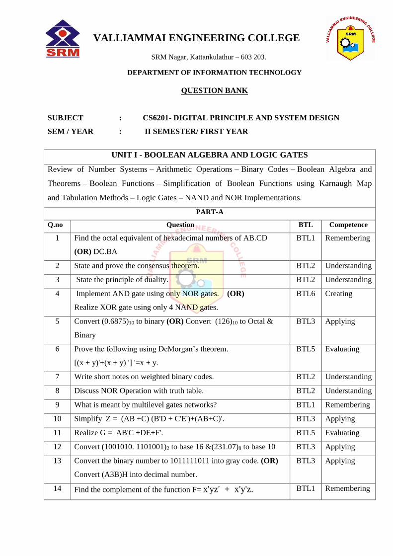
VALLIAMMAI ENGINEERING COLLEGE
SRM Nagar, Kattankulathur – 603 203.
DEPARTMENT OF INFORMATION TECHNOLOGY
QUESTION BANK
SUBJECT : CS6201- DIGITAL PRINCIPLE AND SYSTEM DESIGN
SEM / YEAR : II SEMESTER/ FIRST YEAR
UNIT I - BOOLEAN ALGEBRA AND LOGIC GATES
Review of Number Systems – Arithmetic Operations – Binary Codes – Boolean Algebra and
Theorems – Boolean Functions – Simplification of Boolean Functions using Karnaugh Map
and Tabulation Methods – Logic Gates – NAND and NOR Implementations.
PART-A
Q.no Question BTL Competence
1 Find the octal equivalent of hexadecimal numbers of AB.CD
(OR) DC.BA
BTL1 Remembering
2 State and prove the consensus theorem. BTL2 Understanding
3 State the principle of duality. BTL2 Understanding
4 Implement AND gate using only NOR gates. (OR)
Realize XOR gate using only 4 NAND gates.
BTL6 Creating
5 Convert (0.6875)10 to binary (OR) Convert (126)10 to Octal &
Binary
BTL3 Applying
6 Prove the following using DeMorgan’s theorem.
[(x + y)'+(x + y) '] '=x + y.
BTL5 Evaluating
7 Write short notes on weighted binary codes. BTL2 Understanding
8 Discuss NOR Operation with truth table. BTL2 Understanding
9 What is meant by multilevel gates networks? BTL1 Remembering
10 Simplify Z = (AB +C) (B'D + C'E')+(AB+C)'. BTL3 Applying
11 Realize G = AB'C +DE+F'. BTL5 Evaluating
12 Convert (1001010. 1101001)2 to base 16 &(231.07)8 to base 10 BTL3 Applying
13 Convert the binary number to 1011111011 into gray code. (OR)
Convert (A3B)H into decimal number.
BTL3 Applying
14 Find the complement of the function F= x'yz' + x'y'z. BTL1 Remembering
Page 3
15 What is Excess-3 code? (OR) Define Self complementary Code? BTL1 Remembering
16 What are Universal Gates? Why are they named so? BTL1 Remembering
17 What bit must be complemented to change an ASCII letter from
capital to lower case and vice versa?
BTL1 Remembering
18 Express the following Boolean expression in to minimum number
of literals. xyz + x'y + xyz'.
BTL5 Evaluating
19 What are the limitations of K-map? BTL1 Remembering
20 Plot the following Boolean functions using three variable maps.
F(X,Y,Z)=∑ m(0,2,3,6,7).
BTL3 Applying
PART-B
Q.no Question Marks BTL Competence
1 Minimize the expression using Quine Mc Cluskey
method F=∑m(0,1,9,15,24,29,30) + ∑d(8,11,31).(OR)
Simplify the following switching function using Quine
Mc Cluskey method and realize expression using gates
F(A,B,C,D) = ∑m(0,5,7,8,9,10,11,14,15). (OR)
Reduce the expression using tabulation method.
F(X1, X 2, X 3, X 4, X 5) =
∑m(0,2,4,5,6,7,8,10,14,17,18,21,29,31) + ∑d(11,20,22)
16 BTL2 Understanding
2 Express the following function in a simplified manner
using K map technique (i) G=πM(0,1,3,7,9,11).
(ii) F(W,X,Y,Z)=∑m(0,7,8,9,10,12)+∑d(2,5,13). (OR)
Simplify the following switching function using
karnaugh map method and realize expression using
gates F(A,B,C,D) = ∑m(0,3,5,7,8,9,10,12,15)
16 BTL2 Understanding
3 Simplify the function
F(W,X,Y,Z)=∑m(2,3,12,13,14,15) using Tabulation
method. Implement the simplified function using gates.
16 BTL4 Analyzing
4(a) Simplify the Boolean function in Sum of Products
(SOP) and Product of Sum (POS)
F(W,X,Y,Z)=∑m(0,1,2,5,8,9,10).
10 BTL4 Analyzing
4(b) Design the Boolean function in Karnaugh map and
simplify it F(W,X,Y,Z)=∑m(0,1,2,4,5,6,8,9,12,13,14).
(OR) Minimize the following function using Karnaugh
map F(A,B,C,D)=∑m(0,1,2,3,4,5,6,11,12,13)
06 BTL6 Creating
5 Simplify the following Boolean expression in
(a) Sum of Product
(b) Product of Sum using Karnaugh map
AC' + B'D + A'CD + ABCD.
08+08 BTL4 Analyzing
Page 4
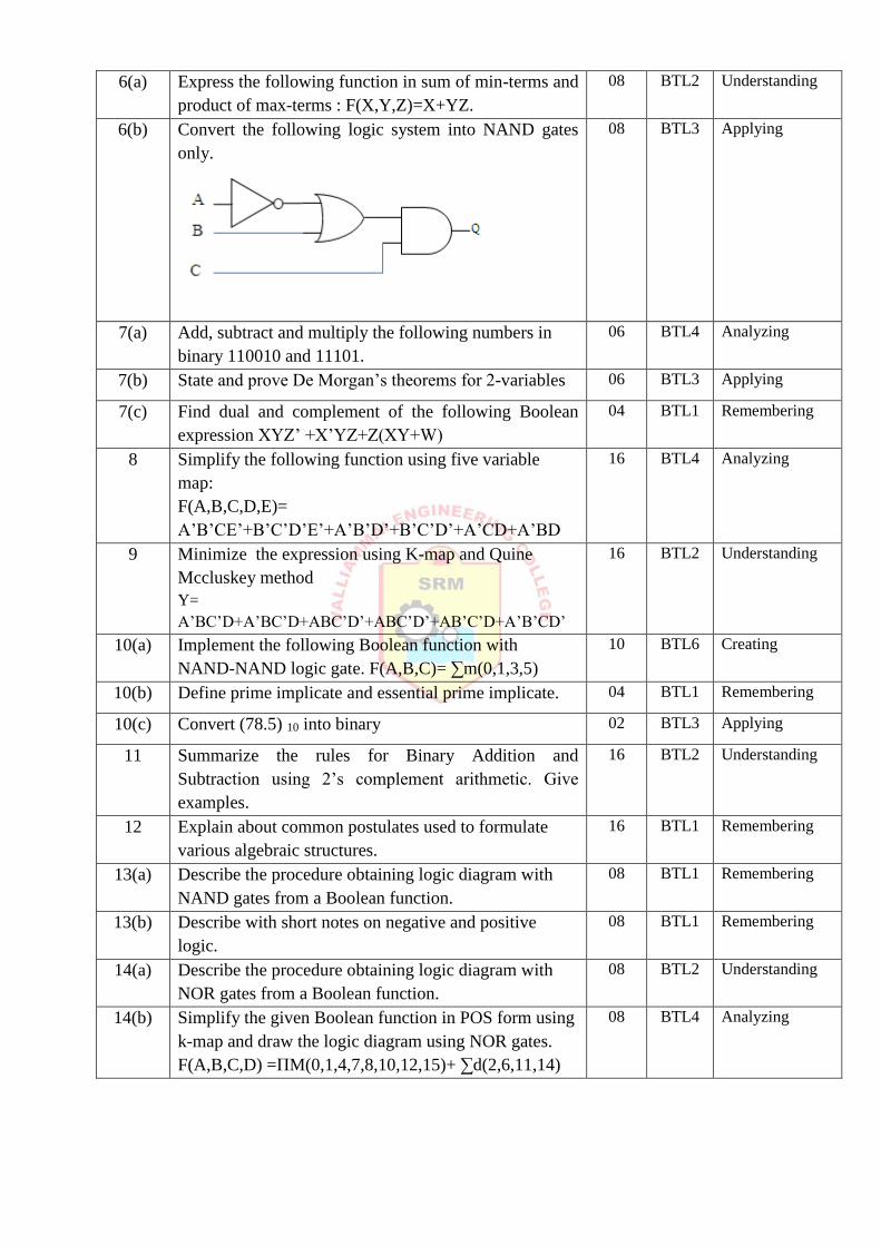
6(a) Express the following function in sum of min-terms and
product of max-terms : F(X,Y,Z)=X+YZ.
08 BTL2 Understanding
6(b) Convert the following logic system into NAND gates
only.
08 BTL3 Applying
7(a) Add, subtract and multiply the following numbers in
binary 110010 and 11101.
06 BTL4 Analyzing
7(b) State and prove De Morgan’s theorems for 2-variables 06 BTL3 Applying
7(c) Find dual and complement of the following Boolean
expression XYZ’ +X’YZ+Z(XY+W)
04 BTL1 Remembering
8 Simplify the following function using five variable
map:
F(A,B,C,D,E)=
A’B’CE’+B’C’D’E’+A’B’D’+B’C’D’+A’CD+A’BD
16 BTL4 Analyzing
9 Minimize the expression using K-map and Quine
Mccluskey method
Y=
A’BC’D+A’BC’D+ABC’D’+ABC’D’+AB’C’D+A’B’CD’
16 BTL2 Understanding
10(a) Implement the following Boolean function with
NAND-NAND logic gate. F(A,B,C)= ∑m(0,1,3,5)
10 BTL6 Creating
10(b) Define prime implicate and essential prime implicate. 04 BTL1 Remembering
10(c) Convert (78.5) 10 into binary 02 BTL3 Applying
11 Summarize the rules for Binary Addition and
Subtraction using 2’s complement arithmetic. Give
examples.
16 BTL2 Understanding
12 Explain about common postulates used to formulate
various algebraic structures.
16 BTL1 Remembering
13(a) Describe the procedure obtaining logic diagram with
NAND gates from a Boolean function.
08 BTL1 Remembering
13(b) Describe with short notes on negative and positive
logic.
08 BTL1 Remembering
14(a) Describe the procedure obtaining logic diagram with
NOR gates from a Boolean function.
08 BTL2 Understanding
14(b) Simplify the given Boolean function in POS form using
k-map and draw the logic diagram using NOR gates.
F(A,B,C,D) =ΠM(0,1,4,7,8,10,12,15)+ ∑d(2,6,11,14)
08 BTL4 Analyzing
Page 5
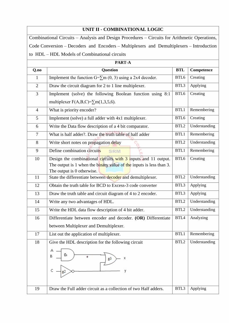
UNIT II - COMBINATIONAL LOGIC
Combinational Circuits – Analysis and Design Procedures – Circuits for Arithmetic Operations,
Code Conversion – Decoders and Encoders – Multiplexers and Demultiplexers – Introduction
to HDL – HDL Models of Combinational circuits
PART-A
Q.no Question BTL Competence
1 Implement the function G=∑m (0, 3) using a 2x4 decoder. BTL6 Creating
2 Draw the circuit diagram for 2 to 1 line multiplexer. BTL3 Applying
3 Implement (solve) the following Boolean function using 8:1
multiplexer F(A,B,C)=∑m(1,3,5,6).
BTL6 Creating
4 What is priority encoder? BTL1 Remembering
5 Implement (solve) a full adder with 4x1 multiplexer. BTL6 Creating
6 Write the Data flow description of a 4 bit comparator. BTL2 Understanding
7 What is half adder?. Draw the truth table of half adder BTL1 Remembering
8 Write short notes on propagation delay BTL2 Understanding
9 Define combination circuits BTL1 Remembering
10 Design the combinational circuits with 3 inputs and 11 output.
The output is 1 when the binary value of the inputs is less than 3.
The output is 0 otherwise.
BTL6 Creating
11 State the differentiate between decoder and demultiplexer. BTL2 Understanding
12 Obtain the truth table for BCD to Excess-3 code converter BTL3 Applying
13 Draw the truth table and circuit diagram of 4 to 2 encoder. BTL3 Applying
14 Write any two advantages of HDL. BTL2 Understanding
15 Write the HDL data flow description of 4 bit adder. BTL2 Understanding
16 Differentiate between encoder and decoder. (OR) Differentiate
between Multiplexer and Demultiplexer.
BTL4 Analyzing
17 List out the application of multiplexer. BTL1 Remembering
18 Give the HDL description for the following circuit
BTL2 Understanding
19 Draw the Full adder circuit as a collection of two Half adders. BTL3 Applying
Page 6
20 The input frequency of a 7497 binary rate multipliers is 64 kHz.
Measure its output be if the multiplier word is 1011. (OR) Point
out the gate level need for carry to propagate from input to
output in ‘n’ bit adder.
BTL5 Evaluating
PART-B
Q.no Question Marks BTL Competence
1 Describe the process involved in converting 8421 BCD
code to Excess 3 code with neat sketch. (OR) Describe the
process involved in converting Excess 3 code to 8421 BCD
code with neat sketch. (OR) Design a code converter that
converts a 8421 to BCD Code .
16 BTL2 Understanding
2(a) Implement the following Boolean function using 8 to 1
Multiplexer. F(A,B,C,D)=A’BD’ + ACD + B'CD + A'C'D.
08 BTL6 Creating
2(b) Implement the above function using 16 to 1 Multiplexer. 08 BTL6 Creating
3 Describe the procedure of converting 8421 to Gray code
converter also realize the converter using only NAND
gates.
16 BTL2 Understanding
4 Design 2-bit magnitude comparator and write a verilog
HDL code.
16 BTL6 Creating
5(a) Implement the following Boolean functions with a
multiplexer. F(w,x,y,z) = ∑m(2,3,5,6,11,14,15) (OR)
Implement the following function using 8 to 1 multiplexer
f(a,b,c,d)= ∑m(0,1,3,5,9,12,14,15) (OR) Implement the
following function using multiplexer f(a,b,c,d)=
∑m(0,1,3,4,8,9,15) .
08 BTL5 Evaluating
5(b) Construct a 5 to 32 line decoder using 3 to 8 line decoders
and 2 to 4 line decoder.
08 BTL6 Creating
6(a) Explain the Analysis procedure. Analyze the following
logic diagram.
08 BTL2 Understanding
Page 7
6(b) With neat diagram explain the 4 bit adder with Carry look
ahead.
08 BTL2 Understanding
7 Design Full subtractor and derive expression for difference
and borrow. Realize using logic gates.
16 BTL6 Creating
8 Design the full adder with inputs x,y,z and two outputs S
and C. The circuits perform x+y+z is the input carry, C is
the output carry and S is the Sum & realize it’s using only
NOR gates.
16 BTL6 Creating
9 Design a logic circuit that accepts a 4-bit grey code and
converts it into 4-bit binary code (OR) Design a binary to
gray code converter circuit (OR) BCD to 7- Segment code
converter circuit.
16 BTL6 Creating
10(a) Design a 2 bit binary multiplier to multiply two binary
numbers and produce a 4-bit result. (OR) Design a 4 bit
magnitude comparator with 3 outputs A>B,A=B,A<B.
12 BTL6 Creating
10(b) Construct a 4-bit odd parity generator circuit using gates. 04 BTL6 Creating
11 Design a combinational circuit to perform BCD addition. 16 BTL6 Creating
12(a) Design 8 to 3 priority encoder. 10 BTL6 Creating
12(b) Realize decode using two 3x 8 decoder with enable input. 06 BTL4 Analyzing
13(a) Explain the design procedure for combinational circuits
with suitable examples.
10 BTL2 Understanding
13(b) Construct 16x1 multiplexer with two 8x1 and 2x1
multiplexer. Use Block diagrams.
06 BTL6 Creating
14(a) Write the HDL gate level description of the priority
encoder circuit.
08 BTL2 Understanding
14(b) Design a 4 –bit parallel binary adder / subtractor. 08 BTL6 Creating
Page 8
UNIT III - SYNCHRONOUS SEQUENTIAL LOGIC
Sequential Circuits – Latches and Flip Flops – Analysis and Design Procedures – State Reduction
and State Assignment – Shift Registers – Counters – HDL for Sequential Logic Circuits.
PART-A
Q.no Question BTL Competence
1 Write the characteristic table and equation of JK flip flop. (OR)
State the excitation table of JK-flip flop.
BTL2 Understanding
2 Write any two application of shift register. BTL2 Understanding
3 With reference to a JK flip flop what is racing? BTL2 Understanding
4 How many states are there in a 3bit ring counter? BTL5 Evaluating
5 What is ring counter? BTL1 Remembering
6 How many states are there in a 3-bit ring counter? what are they? BTL5 Evaluating
7 Give block diagram of Master -Slave D Flip flop BTL2 Understanding
8 Draw the diagram of T- Flip flop and discuss its working. BTL3 Applying
9 What is shift register? (OR) Classify the shift registers. BTL1 Remembering
10 What is the minimum number of Flip flops needed to build a
counter of modulus 8? (OR) Analyze how many Flip-flops are
required to design a synchronous MOD 60 counter?
BTL5 Evaluating
11 Write the HDL code to realize a D - Flip flop. BTL2 Understanding
12 State the rules for state assignment. BTL2 Understanding
13 Realize a JK Flip flop using D flip flop be and gates. BTL3 Applying
14 Write the HDL code for up-down counter using behavioural
model.
BTL2 Understanding
15 Write the characteristic table and equation of SR Flip flop. BTL2 Understanding
16 Explain the difference between the performance of asynchronous
and synchronous counter.
BTL5 Evaluating
17 Differentiate between Latch and Flip flop. BTL4 Analyzing
18 Define Ripple counter. BTL2 Understanding
19 Select and list any two mechanisms to achieve edge triggering of
flip flop.
BTL2 Understanding
20 Design a 4 bit binary synchronous counter with D Flip flops. (OR)
Write down the steps involved in the design of synchronous
sequential circuits.
BTL6 Creating
Page 9
PART-B
Q.no Question Marks BTL Competence
1 Implement T flip-flop using D flip-flop and JK using D flip flop. 16 BTL5 Evaluating
2 Design a synchronous counter which counts in the sequence
000,001,010,011,100,101,110,111,000 using D Flip-flop. (OR)
Design a synchronous counter with the following sequence:
0,1,3,7,6,4 and repeats. Use JK Flip flop.
16 BTL6 Creating
3 Design a MOD-10 Synchronous counter using JK Flip-flop. Write
execution table and state table. (OR) Design MOD 6 counter
circuit.
16 BTL6 Creating
4(a) How a race condition can be avoided in a Flip-flop. 08 BTL4 Analyzing
4(b) Realize the sequential circuit for the state diagram shown below.
08 BTL4 Analyzing
5(a) A sequential circuit with two D Flip-flops A and B, one input x ,
and one output z is specified by the following next state and
output equations: A(t+1) = A'+B; B(t+1)=B'x ; z =A+B'
(i)Draw the logic diagram of the circuit. (04)
(ii)Derive the state table. (03)
(iii)Draw the state diagram of the circuit.(03)
10
BTL3 Applying
5(b) Explain the difference between a state table, characteristic table
and an excitation table.
06 BTL5 Evaluating
6 Consider the design of a 4 bit BCD counter that counts in the
following way: 0000 , 0010 , 0011 , ………. , 1001 , and back to
0000.
(i) Draw the state diagram.(04)
(ii) List the next state table. (04)
16 BTL3 Applying
a/0
c/1
b/0
X=1 X=0,X=1
X=0,X=1
X=0
Page 10
(iii) Draw the logic diagram of the circuit.(08)
7 Design sequence detector that detects a sequence of three or more
consecutive 1’s in a string of bits coming through an input line and
produces an output whenever this sequence is detected.(OR)
Design a sequence detector to detect the input sequence
101(overlapping ).Use JK Flip flops.
16 BTL6 Creating
8 Design a three bit synchronous counter with T flip flop and draw
the diagram.
16 BTL6 Creating
9 Design the sequential circuit specified by the following state
diagram using T flip flops.
16 BTL6 Creating
10(a) Design a 3-bit synchronous up counter using JK flip flop 06 BTL6 Creating
10(b) Design 3 bit parallel in serial out shift register and write the HDL
code to realize it.
10 BTL6 Creating
11 Design a sequential circuit with two T Flip flop A and B , one
input x and one output z is specified by the following next state
and output equation is
A(t+1)= BX’+B’X; B(t+1)=AB+BX+AX; Z=AX’+A’B’X
(i) Draw the logic diagram of the circuit. (ii) List the state table for
16 BTL6 Creating
Page 11
the sequential circuit (iii) Draw the Corresponding state diagram.
12 Explain the operation of master slave flip flop and show how the
race around condition is eliminated in it.
16 BTL5 Evaluating
13 Write the HDL description of T flip-flop , JK flip-flop ,SR flip
flop and D flip-flops. (OR) Design a serial adder using a full adder
and a flip flop
16 BTL2 Understanding
14(a) Draw the block diagram of Johnson counter and explain it. 08 BTL2 Understanding
14(b) Discuss the different types of shift registers with neat diagram. 08 BTL1 Remembering
UNIT IV- ASYNCHRONOUS SEQUENTIAL LOGIC
Analysis and Design of Asynchronous Sequential Circuits – Reduction of State and Flow Tables
–Race-free State Assignment – Hazards.
PART-A
Q.no Question BT Level Competence
1 Define race conditions.(OR)What is critical race condition?
Give example.
BTL1 Remembering
2 What are the types of hazards? BTL1 Remembering
3 Define hazards. BTL1 Remembering
4 Distinguish Moore and Mealy circuit. BTL4 Analyzing
5 Define Essential hazards. BTL1 Remembering
6 Compare asynchronous and synchronous sequential circuit. BTL3 Applying
7 What are cycles and races? BTL2 Understanding
8 Define the critical race and non critical race. BTL1 Remembering
9 What is lockout? How it is avoided? BTL2 Understanding
10 Draw the wave forms showing static 1 hazards (OR) Write short
notes on Static -1 hazards.
BTL3 Applying
11 Distinguish fundamental mode circuit and pulse mode circuit. BTL4 Analyzing
12 Define primitive flow table. BTL2 Understanding
13 Show the diagram for debounce circuit. BTL3 Applying
14 Compare basic of fundamental mode circuit and pulse mode
circuit.
BTL2 Understanding
Page 12
15 Summarize the steps involved in the designing an asynchronous
sequential circuits.
BTL2 Understanding
16 How can we change the hazards into hazards free circuit? BTL5 Evaluating
17 How the flow table differ from transition table? BTL1 Remembering
18 Compare static and dynamic hazards. BTL4 Analyzing
19 Is it essential to have race free assignment? Justify. BTL5 Evaluating
20 Discuss about conventional flow table and primitive flow table. BTL6 Creating
PART-B
Q.no Question Marks BTL Competence
1 Explain the steps for the design of asynchronous
sequential circuits with an example.
16 BTL2 Understanding
2 Implement the switching function
F=∑m(1,3,5,7,8,9,14,15) by a static hazard free two
level AND-OR gate network.
16 BTL6 Creating
3 An asynchronous sequential circuit is described by the
following excitation and output function.
Y=X1X2+(X2+X3)Y and Z=Y
1. Draw the logic diagram of the circuit. (06)
2. Derive the transition table and output map.(06)
3. Describer the behaviour of the circuit.(04)
16 BTL3 Applying
4 Analyze the following clocked sequential circuit and
obtain the state equation and state diagram.
16 BTL4 Analyzing
5(a) Find a critical race free state assignment for the reduced
flow table shown.
08 BTL4 Analyzing
5(b) Reduce the number of state in the following state 08 BTL5 Evaluating
Page 13
diagram. Tabulate the reduced state and draw the
reduced diagram.
Present state Next state Output
x=0 x=1 x=0 x=1
a a b 0 0
b c d 0 0
c a d 0 0
d e f 0 1
e a f 0 1
f g f 0 1
g a f 0 1
6 Explain the hazards in combinational circuit and
sequential circuit and also demonstrate a hazards and
its removal with example.
16 BTL4 Analyzing
7 Design an asynchronous sequential circuit with 2 inputs
X and Y and with one output Z wherever Y is 1, input X
is transferred to Z. When Y is 0; the output does not
change for any change in X. Use SR latch for
implementation of the circuit.
16 BTL6 Creating
8 Discuss in detail the procedure for reducing the flow
table with an example.
16 BTL2 Understanding
9(a) Explain the types of asynchronous sequential circuit. 08 BTL5 Evaluating
9(b) Derive a circuit specified by the following flow table.
08 BTL1 Remembering
10(a) What is the objective of state assignment in
asynchronous circuit? Explain race free state assignment
with an example.
08 BTL1 Remembering
10(b) Discuss about static, dynamic and essential hazards in
asynchronous sequential circuits.
08 BTL2 Understanding
Page 14
11 How to design an asynchronous sequential circuit with
inputs X1 and X2 and one output Z. Initially and at any
time if both the inputs are 0, output is equal to 0.When
X1 or X2 becomes 1, Z becomes 1. When Second input
also becomes 1, Z=0; The output stays at 0 until circuit
goes back to initial state.
16 BTL1 Remembering
12 How to design an asynchronous sequential circuit with
two input x and y and with one output z whenever y is 1,
input x is transferred to z. When y is 0, the output does
not change for any change in x.
16 BTL1 Remembering
13 Explain with a neat example for minimization of
primitive flow table.
16 BTL5 Evaluating
14 An asynchronous sequential circuit is described by the
following excitation and output function. X =
(Y1Z1'W2)X + (Y1'Z1W2') & S = X'
(i) Draw the logic diagram of the circuit. (06)
(ii) Derive the transition table and output map.(06)
(iii) Describe the behavior of the circuit. (04)
16 BTL3 Applying
UNIT V - MEMORY AND PROGRAMMABLE LOGIC
RAM and ROM – Memory Decoding – Error Detection and Correction – Programmable Logic
Array – Programmable Array Logic – Sequential Programmable Devices – Application Specific
Integrated Circuits.
PART-A
Q.no Question BTL Competence
1 What is memory decoding? BTL1 Remembering
2 Define ASIC. BTL2 Understanding
3 Justify whether PAL is same as PLA. BTL5 Evaluating
4 What is volatile memory? Give example. BTL1 Remembering
5 Differentiate between EEPROM and PROM. BTL4 Analyzing
6 How to detect double error and correct single error? BTL4 Analyzing
7 What is memory address register? BTL1 Remembering
8 Write short notes on PLA. BTL2 Understanding
Page 15
9 A seven bit hamming code is received as 1111110. What is the
correct code?
BTL1 Applying
10 List the types of memories. BTL1 Remembering
11 Define combinational PLD. BTL1 Remembering
12 Draw the logic diagram of one bit static RAM cell. BTL3 Applying
13 Calculate the maximum range of a memory that can be accessed
using 10 address lines.
BTL5 Evaluating
14 Discuss the features of PROM and PLD. BTL6 Creating
15 How to apply the error detection and correction technique. BTL3 Applying
16 Identify the operations involved in RAM. BTL5 Evaluating
17 Design the logic diagram of a memory cell. BTL6 Creating
18 Write down the different types of PLDs. BTL2 Understanding
19 Classify the types of RAM. BTL2 Understanding
20 Differentiate between PLA and ROM. BTL4 Analyzing
PART-B
Q.no Question Marks BTL Competence
1 Implement the following function using PLA
A(X,Y,Z)=∑m(1,2,4,6); B(X,Y,Z)=∑m(0,1,6,7);
C(X,Y,Z)=∑m(2,6)
16 BTL5 Evaluating
2 The following message have been coded in the even parity
hamming code and transmitted through a noisy channel.
Decode the message assuming that at most a single error
occurred in each codeword.
i) 1001001 (04) ii) 0111001 (04)
iii) 1110110 (04) iv) 0011011 (04)
16 BTL3 Applying
3 Design a BCD to Excess 3 code converter and implement
using suitable PLA.
16 BTL6 Creating
4 Discuss the concept of working and application of
semiconductor memories.
16 BTL1 Remembering
5(a) Write short notes on Address Multiplexing. 08 BTL2 Understanding
5(b) Briefly discuss the sequential programmable devices. 08 BTL1 Remembering
6(a) Implement the following Two Boolean function with a PLA 10 BTL5 Evaluating
Page 16
F1=AB'+AC+A'BC' F2=(AC+BC) '
6(b) Give the Internal block diagram of 4 x 4 RAM. 06 BTL2 Understanding
7 Implement the following using PAL, F1(A,B,C)= ∑(1,2,4,6);
F2(A,B,C) =∑(0,1,6,7) ; F3(A,B,C)= ∑(1,2,3,5,7)
16 BTL5 Evaluating
8 Design a combinational circuit using ROM that accepts a three
bit binary number and outputs a binary number equal to the
square of the input number.
16 BTL6 Creating
9 Draw a neat sketch showing implementation of Z1= ab’d’e +
a’b’c’e+bc+de; Z2= a’c’e; Z3=bc+de+c’d’e+db and Z4=a’c’e
using 5*8*4 PLA.
16 BTL3 Applying
10(a) Illustrate the two following Boolean functions using 8X2
PROM. F1=∑m(3,5,6,7) and F2=∑m(1,2,3,4)
06 BTL2 Understanding
10(b) Illustrate the following two Boolean functions using PLA
with 3 inputs, 4 Product terms, and 2 outputs.
F1=∑m(3,5,6,7) and F2=∑m(1,2,3,4)
10 BTL2 Understanding
11 Examine the following using PAL
W(A,B,C,D) = ∑(0,2,6,7,8,9,12,13);
X(A,B,C,D) =∑(0,2,6,7,8,9,12,13,14) ;
Y(A,B,C,D) = ∑(2,3,8,9,10,12,13);
Z(A,B,C,D)= ∑(1,3,4,6,9,12,14);
16 BTL4 Analyzing
12 Discuss the sequential programmable devices. 16 BTL1 Remembering
13(a) Compare PROM, PLA, PAL. 08 BTL4 Analyzing
13(b) Compare SRAM and DRAM. 08 BTL4 Analyzing
14 Discuss the various types of RAM and ROM with architecture. 16 BTL1 Remembering
Course In charge
1.................................................
2.................................................
3.................................................