Page 1
VANADIUM DIOXIDE-BASED MATERIALS FOR POTENTIAL THERMAL SWITCHING
APPLICATIONS
By
Minyoung Jeong
A THESIS
Submitted to
Michigan State University
in partial fulfillment of the requirements
for the degree of
Materials Science and Engineering – Master of Science
2013
Page 2
ABSTRACT
VANADIUM DIOXIDE-BASED MATERIALS FOR POTENTIAL THERMAL SWITCHING
APPLICATIONS
By
Minyoung Jeong
One of the materials able to exhibit a transition from insulators to metals (IMT materials)
is vanadium dioxide (VO2). Through IMT, VO2 shows a drop of resistivity of five orders of
magnitude at a picosecond timescale. In this work, the feasibility of using VO2 as an efficient
thermal switching device is discussed.
Several synthesis methods (sol-gel, hot press and spark plasma sintering) were attempted
to obtain VO2 sample in pellet form. From the X-ray diffraction results, it was found that spark
plasma sintering (SPS) yielded the highest phase purity. Several sintering parameters such as
temperature or sintering time were tested to determine the optimal sintering conditions.
For better thermal switching behavior, high-energy ball milling was used to reduce lattice
thermal conductivity ( in the insulator phase. Ball-milling time was varied from 30
minutes to 2 hours. It was found that with increasing milling time, the was reduced. Thus, it
was demonstrated that thermal switching behavior was most efficient with 2 hour-milling.
To improve electronic thermal conductivity ( ) in the metallic state, nano-sized
copper particles were added to the VO2 system with a subtle amount variation ranging from 3at %
to 5 at%. Results show that a composite with 5 at% Cu (copper) addition exhibited the largest
increase in thermal conductivity ( in the metallic state.
Page 3
iv
ACKNOWLEDGEMENTS
It is by far my great honor to present my work conducted at Michigan State University
for two years. Things I have learned in those two years not only include the knowledge and
research skills required to be a professional engineer, but also include what it takes to live a
successful life, for example, self-control, passion and so on. For this reason, I feel very grateful
for all the support that my advisor, Dr.Morelli, gave to me through the past years. From him, I
learned many lessons how to be a committed engineer while at the same time, how to be a
mature and intellectual adult.
I deeply appreciate comments and encouragements my committee professors
(Dr.Sakamoto, Dr.Nicholas and Dr.Hogan) gave on my work. I also want to thank my lab-mates
(Xu Lu, Stephen Boona, Gloria Lehr and Vijay Ponnambalam) for their eagerness to help and for
their friendliness.
Finally, I want to give many thanks to all the members at my church, Lansing Korean
United Methodist Church, for their great support and sincere prayers for me. Pastor Cho and
Mrs.Cho, without you, this thesis would have been an impossible task for me.
I always love my family, and it is definitely the most thankful and biggest gift for me to be one
of them.
Page 4
v
TABLE OF CONTENTS
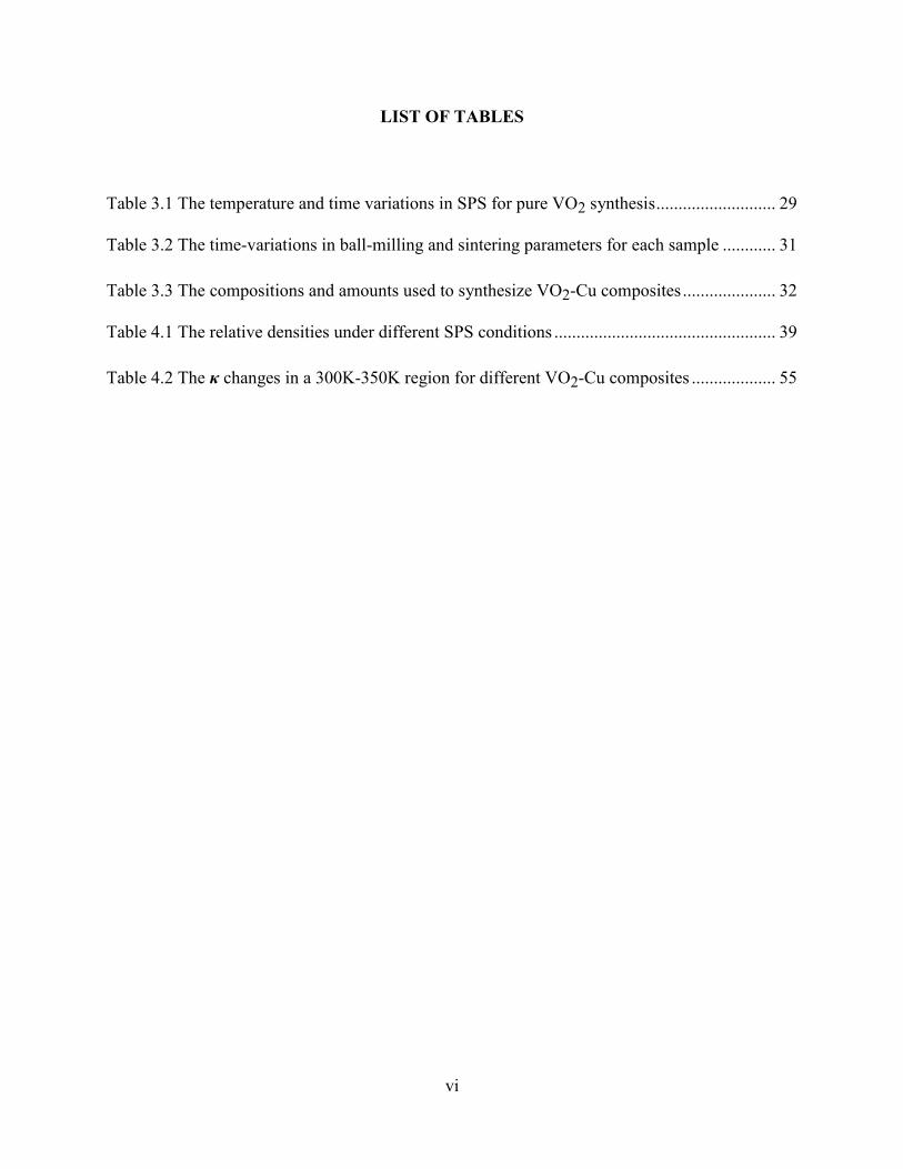
LIST OF TABLES……………………………………………………………………………..…vi
LIST OF FIGURES ...................................................................................................................... vii
CHAPTER 1. INTRODUCTION ................................................................................................... 1
CHAPTER 2. BACKGROUND AND MOTIVATION ................................................................. 3
2.1 Band theory of solids........................................................................................................ 3
2.2 Insulator to Metal Transition (IMT) phenomena ............................................................. 4
2.3 Basic IMT mechanisms .................................................................................................... 8
2.4 Applications of IMT ....................................................................................................... 12
2.5 Thermal switching .......................................................................................................... 15
2.6 Vanadium dioxide for thermal switching ....................................................................... 18
2.7 Summary ........................................................................................................................ 24
CHAPTER 3. METHODS AND PROCEDURES ....................................................................... 25
3.1 Synthesizing pure VO2 ................................................................................................... 25
i) Materials ......................................................................................................................... 25
i) Procedures ...................................................................................................................... 26
3.2 Synthesizing VO2-Cu Composites ................................................................................. 31
i) Materials ......................................................................................................................... 31
ii) Procedures ...................................................................................................................... 31
3.3 Transport Property Measurements ................................................................................. 32
CHAPTER 4. RESULTS AND DISCUSSION ............................................................................ 35
4.1 VO2 Synthesis ................................................................................................................. 35
i) Hot Pressed Specimens .................................................................................................. 35
ii) Spark Plasma Sintered Specimens ................................................................................. 38
iii) Sol-Gel Technique Specimens .................................................................................... 44
4.2 Modifications on VO2 specimens ................................................................................... 45
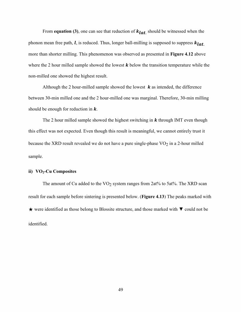
i) High-energy ball-milling ................................................................................................ 45
ii) VO2-Cu Composites ....................................................................................................... 49
CHAPTER 5. Conclusions............................................................................................................ 57
CHAPTER 6. FUTURE RESEARCH CONSIDERATIONS ...................................................... 58
BIBLIOGRAPHY ......................................................................................................................... 60
Page 5
vi
LIST OF TABLES
Table 3.1 The temperature and time variations in SPS for pure VO2 synthesis ........................... 29
Table 3.2 The time-variations in ball-milling and sintering parameters for each sample ............ 31
Table 3.3 The compositions and amounts used to synthesize VO2-Cu composites ..................... 32
Table 4.1 The relative densities under different SPS conditions .................................................. 39
Table 4.2 The κ changes in a 300K-350K region for different VO2-Cu composites ................... 55
Page 6
vii
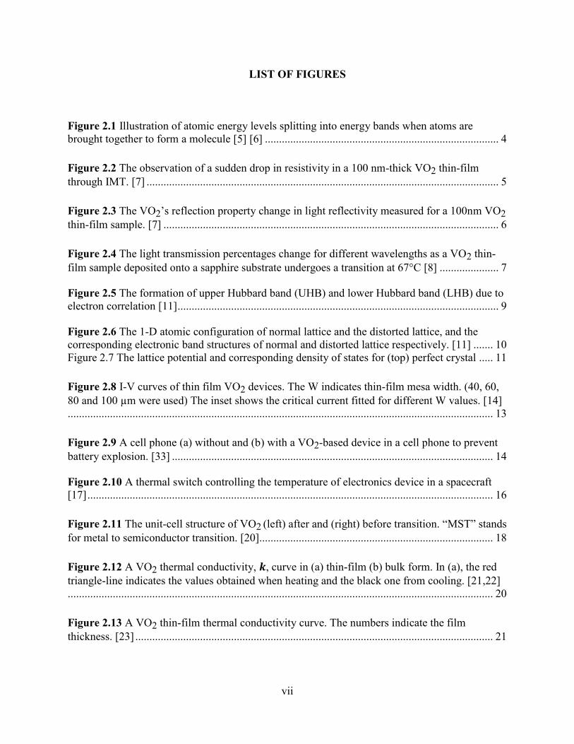
LIST OF FIGURES
Figure 2.1 Illustration of atomic energy levels splitting into energy bands when atoms are
brought together to form a molecule [5] [6] ................................................................................... 4
Figure 2.2 The observation of a sudden drop in resistivity in a 100 nm-thick VO2 thin-film
through IMT. [7] ............................................................................................................................. 5
Figure 2.3 The VO2’s reflection property change in light reflectivity measured for a 100nm VO2
thin-film sample. [7] ....................................................................................................................... 6
Figure 2.4 The light transmission percentages change for different wavelengths as a VO2 thin-
film sample deposited onto a sapphire substrate undergoes a transition at 67°C [8] ..................... 7
Figure 2.5 The formation of upper Hubbard band (UHB) and lower Hubbard band (LHB) due to
electron correlation [11] .................................................................................................................. 9
Figure 2.6 The 1-D atomic configuration of normal lattice and the distorted lattice, and the
corresponding electronic band structures of normal and distorted lattice respectively. [11] ....... 10
Figure 2.7 The lattice potential and corresponding density of states for (top) perfect crystal ..... 11
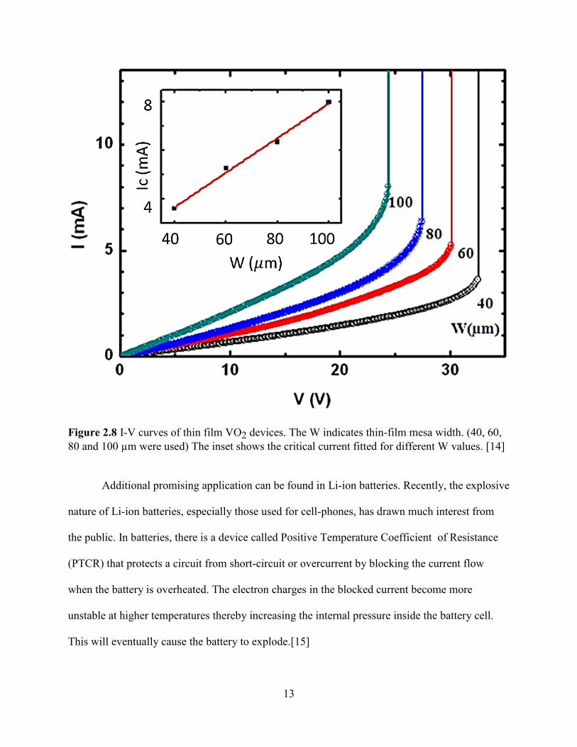
Figure 2.8 I-V curves of thin film VO2 devices. The W indicates thin-film mesa width. (40, 60,
80 and 100 µm were used) The inset shows the critical current fitted for different W values. [14]
....................................................................................................................................................... 13
Figure 2.9 A cell phone (a) without and (b) with a VO2-based device in a cell phone to prevent
battery explosion. [33] .................................................................................................................. 14
Figure 2.10 A thermal switch controlling the temperature of electronics device in a spacecraft
[17] ................................................................................................................................................ 16
Figure 2.11 The unit-cell structure of VO2 (left) after and (right) before transition. “MST” stands
for metal to semiconductor transition. [20]................................................................................... 18
Figure 2.12 A VO2 thermal conductivity, , curve in (a) thin-film (b) bulk form. In (a), the red
triangle-line indicates the values obtained when heating and the black one from cooling. [21,22]
....................................................................................................................................................... 20
Figure 2.13 A VO2 thin-film thermal conductivity curve. The numbers indicate the film
thickness. [23] ............................................................................................................................... 21
Page 7
viii
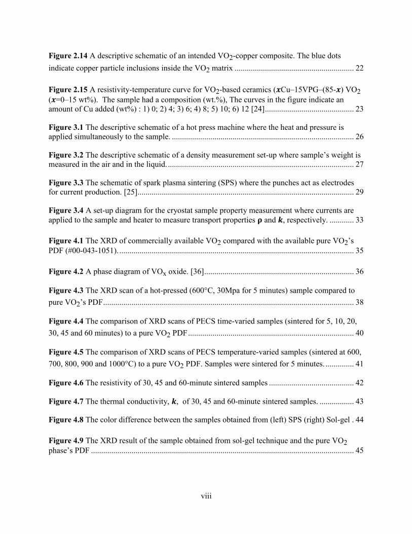
Figure 2.14 A descriptive schematic of an intended VO2-copper composite. The blue dots
indicate copper particle inclusions inside the VO2 matrix ........................................................... 22
Figure 2.15 A resistivity-temperature curve for VO2-based ceramics ( Cu–15VPG–(85- ) VO2
( =0–15 wt%). The sample had a composition (wt.%), The curves in the figure indicate an
amount of Cu added (wt%) : 1) 0; 2) 4; 3) 6; 4) 8; 5) 10; 6) 12 [24] ............................................ 23
Figure 3.1 The descriptive schematic of a hot press machine where the heat and pressure is
applied simultaneously to the sample. .......................................................................................... 26
Figure 3.2 The descriptive schematic of a density measurement set-up where sample’s weight is
measured in the air and in the liquid. ............................................................................................ 27
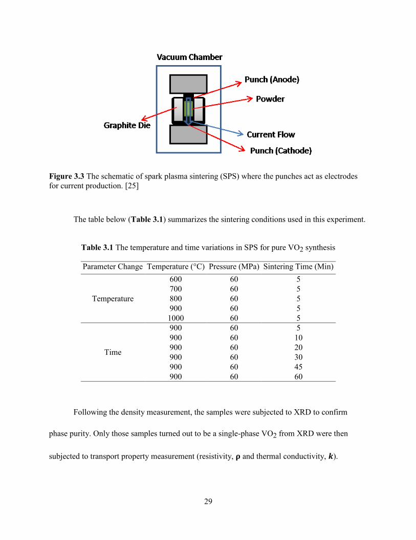
Figure 3.3 The schematic of spark plasma sintering (SPS) where the punches act as electrodes
for current production. [25] ........................................................................................................... 29
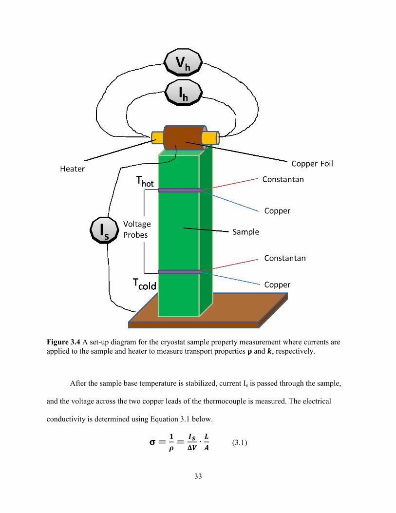
Figure 3.4 A set-up diagram for the cryostat sample property measurement where currents are
applied to the sample and heater to measure transport properties and , respectively. ............ 33
Figure 4.1 The XRD of commercially available VO2 compared with the available pure VO2’s
PDF (#00-043-1051). .................................................................................................................... 35
Figure 4.2 A phase diagram of VOx oxide. [36] .......................................................................... 36
Figure 4.3 The XRD scan of a hot-pressed (600°C, 30Mpa for 5 minutes) sample compared to
pure VO2’s PDF ............................................................................................................................ 38
Figure 4.4 The comparison of XRD scans of PECS time-varied samples (sintered for 5, 10, 20,
30, 45 and 60 minutes) to a pure VO2 PDF .................................................................................. 40
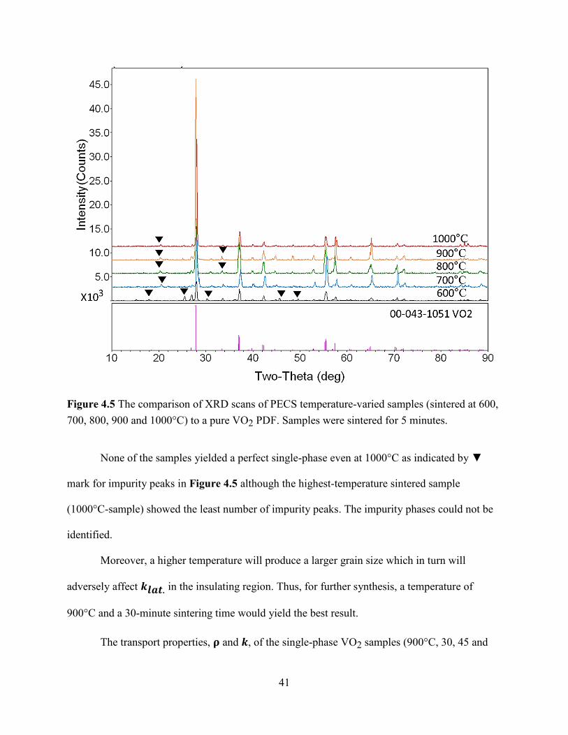
Figure 4.5 The comparison of XRD scans of PECS temperature-varied samples (sintered at 600,
700, 800, 900 and 1000°C) to a pure VO2 PDF. Samples were sintered for 5 minutes. .............. 41
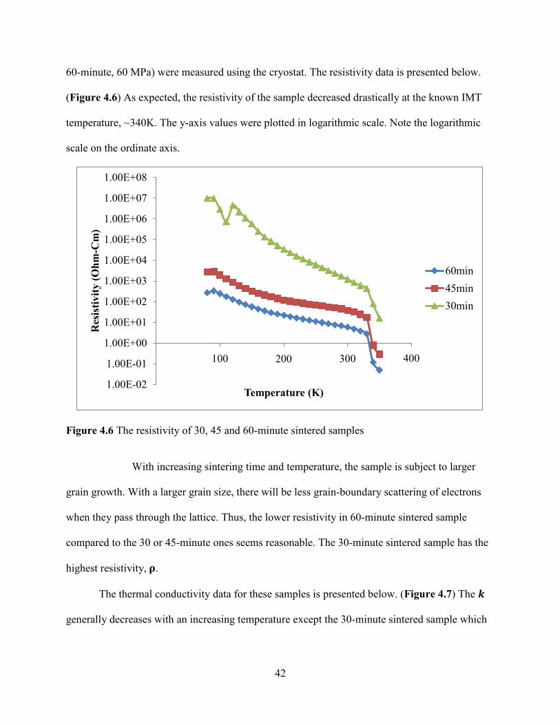
Figure 4.6 The resistivity of 30, 45 and 60-minute sintered samples .......................................... 42
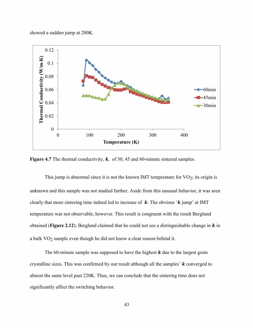
Figure 4.7 The thermal conductivity, , of 30, 45 and 60-minute sintered samples. ................. 43
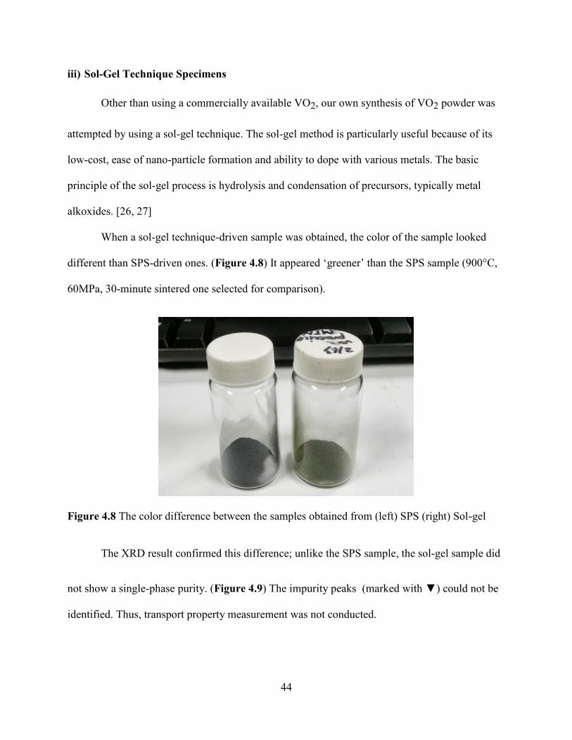
Figure 4.8 The color difference between the samples obtained from (left) SPS (right) Sol-gel . 44
Figure 4.9 The XRD result of the sample obtained from sol-gel technique and the pure VO2
phase’s PDF .................................................................................................................................. 45
Page 8
ix
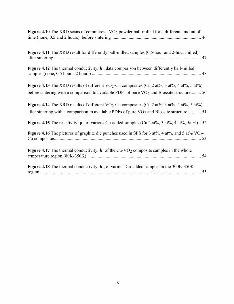
Figure 4.10 The XRD scans of commercial VO2 powder ball-milled for a different amount of
time (none, 0.5 and 2 hours) before sintering .............................................................................. 46
Figure 4.11 The XRD result for differently ball-milled samples (0.5-hour and 2-hour milled)
after sintering ................................................................................................................................ 47
Figure 4.12 The thermal conductivity, , data comparison between differently ball-milled
samples (none, 0.5 hours, 2 hours) ............................................................................................... 48
Figure 4.13 The XRD results of different VO2-Cu composites (Cu 2 at%, 3 at%, 4 at%, 5 at%)
before sintering with a comparison to available PDFs of pure VO2 and Blossite structure ......... 50
Figure 4.14 The XRD results of different VO2-Cu composites (Cu 2 at%, 3 at%, 4 at%, 5 at%)
after sintering with a comparison to available PDFs of pure VO2 and Blossite structure............ 51
Figure 4.15 The resistivity, , of various Cu-added samples (Cu 2 at%, 3 at%, 4 at%, 5at%) .. 52
Figure 4.16 The pictures of graphite die punches used in SPS for 3 at%, 4 at%, and 5 at% VO2-
Cu composites ............................................................................................................................... 53
Figure 4.17 The thermal conductivity, , of the Cu-VO2 composite samples in the whole
temperature region (80K-350K) ................................................................................................... 54
Figure 4.18 The thermal conductivity, , of various Cu-added samples in the 300K-350K
region ............................................................................................................................................ 55
Page 9
1
CHAPTER 1. INTRODUCTION
Currently, electronics are getting smaller and more compact. However, the amount of
information processed by the devices has increased tremendously. Moreover, people want their
devices to have higher power-efficiency for longer uses.
To achieve a more power-efficient electronic device while maintaining a fast processing
speed and compact size, conventional electric circuit components need a breakthrough. One of
such components is a transistor.
Transistors control the flow of current inside a circuit to amplify or switch electric signals
depending on the application of external voltage.[1] If we can construct a transistor that can
switch ‘on and off’ efficiently at an ultrafast timescale without adding extra components or
without complicated algorithms, a breakthrough for a faster yet smaller electronic device would
be realized.
In this perspective, insulator metal transition (IMT) phenomena can be found very useful
because it typically occurs with a simple electric field or temperature change. Also, this
transition occurs through the bulk of crystal thereby freeing the size limit of the device. Thus,
there are many works being conducted on realization of IMT-based transistors.[2]
Not only do the electrical properties change through IMT, but also the thermal
conductivity should change when a material undergoes a transition from insulator to metal or
vice versa. If we can utilize this, an efficient thermal switching device for directing a heat flow
or for maintaining a ‘set’ temperature could be constructed.
It is desirable if we can make this switching occur faster and show a very sharp
distinguishable difference between two different states for switching applications.
Page 10
2
In this work, the possible applications of vanadium dioxide (VO2), a well-known IMT
material as a thermal switch was explored. To achieve a much sharper thermal conductivity ( )
distinction between the two states for better thermal switching behavior, should be enhanced in
the metallic phase while reduced in the insulator phase.
For this purpose, the following was set as the main objectives of this study :
(1) synthesizing phase-pure VO2 with various synthesis methods and conditions; (2) utilizing
increased grain boundary scattering to reduce the lattice thermal conductivity on the insulating
side of the transition, and (3) utilizing a concept of composite material for better switching
behavior of VO2.
Page 11
3
CHAPTER 2. BACKGROUND AND MOTIVATION
2.1 Band theory of solids
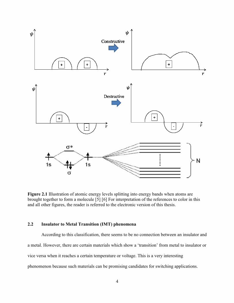
When the two atoms are brought closer together, the electron wave functions start
overlapping together. The overlapping occurs in constructive or destructive manners. This results
in molecular bonding and anti-bonding.[3]
In a crystal lattice, there are countless atom-atom interactions. Therefore, the overlapping
of different wave functions will create many different wave curve combinations, leading to
accumulation of band splitting. This accumulation of splitting creates a continuous energy bands
separated by an ‘empty space’ in the middle. This empty space is called a forbidden band, an
origin of energy band gap. The figure below (Figure 2.1) is a descriptive presentation of this
phenomenon. Here, hydrogen molecules were used as an example. [4] [5] [6]
The allowed band located below the gap is called a valence band, and the one located
above is called a conduction band. Using this energy band theory, conductors, insulators and
semiconductors can be differentiated.
In good conductors such as bands are half-filled valence and electrons can move to
nearby energy states very easily without requiring much additional energy. [4] On the other hand,
a large energy gap exists between the conduction and valence bands in insulators. Thus, electrons
cannot move easily without a significantly large potential difference. This makes insulators poor
conductors
Page 12
4
Figure 2.1 Illustration of atomic energy levels splitting into energy bands when atoms are
brought together to form a molecule [5] [6] For interpretation of the references to color in this
and all other figures, the reader is referred to the electronic version of this thesis.
2.2 Insulator to Metal Transition (IMT) phenomena
According to this classification, there seems to be no connection between an insulator and
a metal. However, there are certain materials which show a ‘transition’ from metal to insulator or
vice versa when it reaches a certain temperature or voltage. This is a very interesting
phenomenon because such materials can be promising candidates for switching applications.
Page 13
5
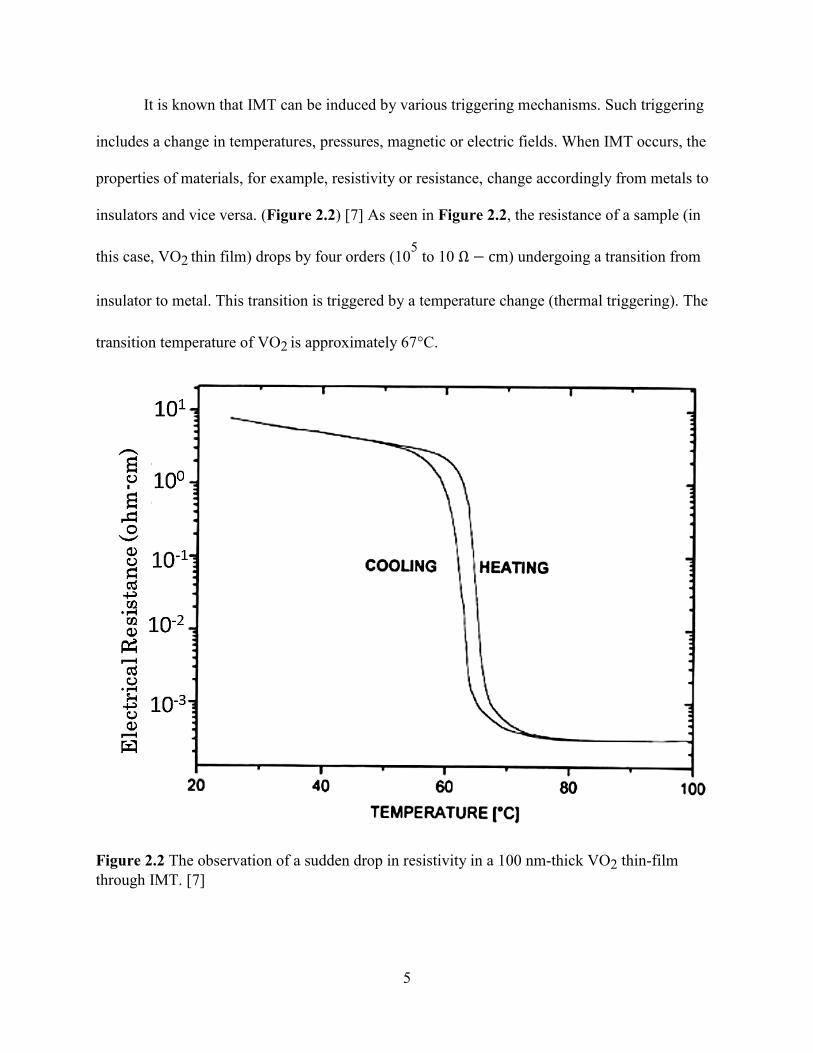
It is known that IMT can be induced by various triggering mechanisms. Such triggering
includes a change in temperatures, pressures, magnetic or electric fields. When IMT occurs, the
properties of materials, for example, resistivity or resistance, change accordingly from metals to
insulators and vice versa. (Figure 2.2) [7] As seen in Figure 2.2, the resistance of a sample (in
this case, VO2 thin film) drops by four orders (105 to 10 ) undergoing a transition from
insulator to metal. This transition is triggered by a temperature change (thermal triggering). The
transition temperature of VO2 is approximately 67°C.
Figure 2.2 The observation of a sudden drop in resistivity in a 100 nm-thick VO2 thin-film
through IMT. [7]
Page 14
6
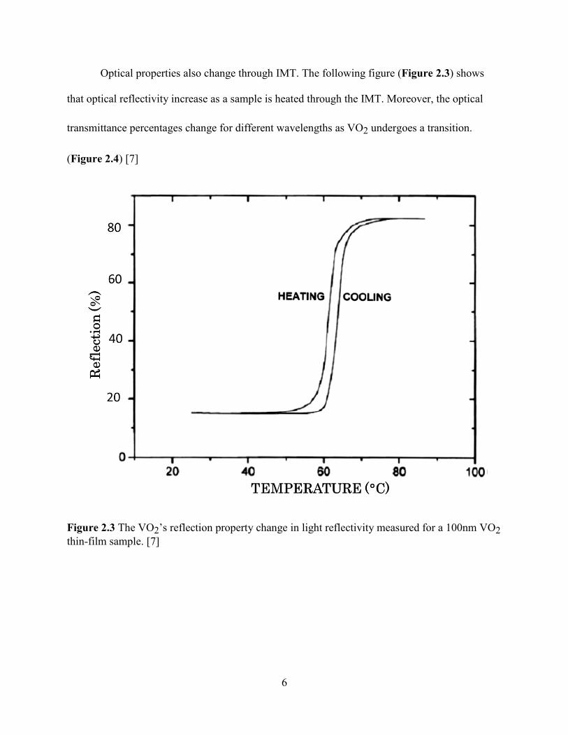
Optical properties also change through IMT. The following figure (Figure 2.3) shows
that optical reflectivity increase as a sample is heated through the IMT. Moreover, the optical
transmittance percentages change for different wavelengths as VO2 undergoes a transition.
(Figure 2.4) [7]
Figure 2.3 The VO2’s reflection property change in light reflectivity measured for a 100nm VO2
thin-film sample. [7]
Page 15
7
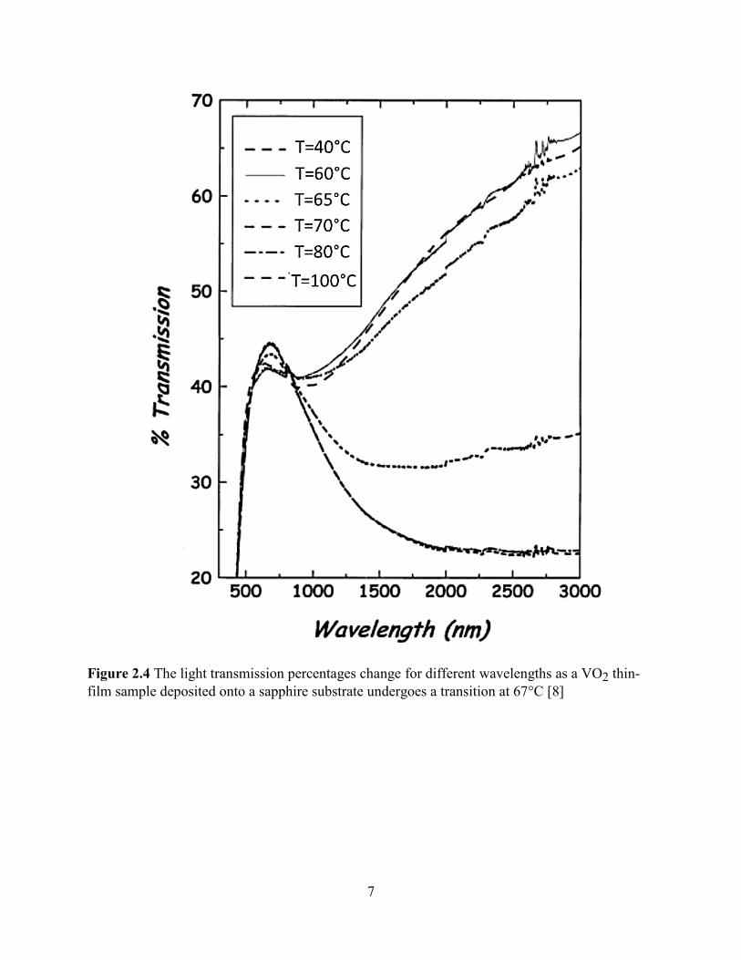
Figure 2.4 The light transmission percentages change for different wavelengths as a VO2 thin-
film sample deposited onto a sapphire substrate undergoes a transition at 67°C [8]
Page 16
8
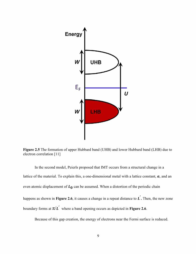
2.3 Basic IMT mechanisms
Even though IMT phenomenon has been discussed for more than 60 years, the primary
mechanism behind IMT is still under debate. Currently, three theories (Mott, Peierls, Anderson)
are widely accepted. [9]
According to Mott’s theory, when the carrier density exceeds a critical carrier density,
which can be calculated from where is the Bohr radius of the
material, the electron-electron interaction such as correlation occurs. He proposed this interaction
leads to a phase transition. [10]
If it is assumed conduction happens by hopping of electrons from one site to another in a
crystal lattice, the Coulomb repulsion occurs when there is an electron already occupied in the
new site. When this repulsion energy U is much greater than electrons’ kinetic energy, the
electrons would not be able to travel through the lattice. [11]
This localization of electrons leads to a formation of two separate bands, UHB (upper
Hubbard band) and LHB (lower Hubbard band), resulting in an insulating phase. This can be
converted back to a metallic state by applying stress to shorten the atomic spacing or doping.
(Figure 2.5)
Page 17
9
Figure 2.5 The formation of upper Hubbard band (UHB) and lower Hubbard band (LHB) due to
electron correlation [11]
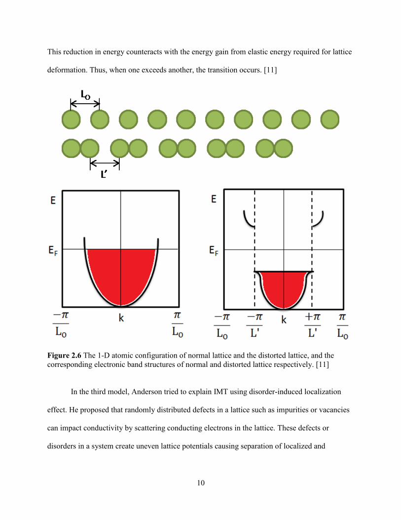
In the second model, Peierls proposed that IMT occurs from a structural change in a
lattice of the material. To explain this, a one-dimensional metal with a lattice constant, , and an
even atomic displacement of can be assumed. When a distortion of the periodic chain
happens as shown in Figure 2.6, it causes a change in a repeat distance to . Then, the new zone
boundary forms at π/ where a band opening occurs as depicted in Figure 2.6.
Because of this gap creation, the energy of electrons near the Fermi surface is reduced.
Page 18
10
This reduction in energy counteracts with the energy gain from elastic energy required for lattice
deformation. Thus, when one exceeds another, the transition occurs. [11]
Figure 2.6 The 1-D atomic configuration of normal lattice and the distorted lattice, and the
corresponding electronic band structures of normal and distorted lattice respectively. [11]
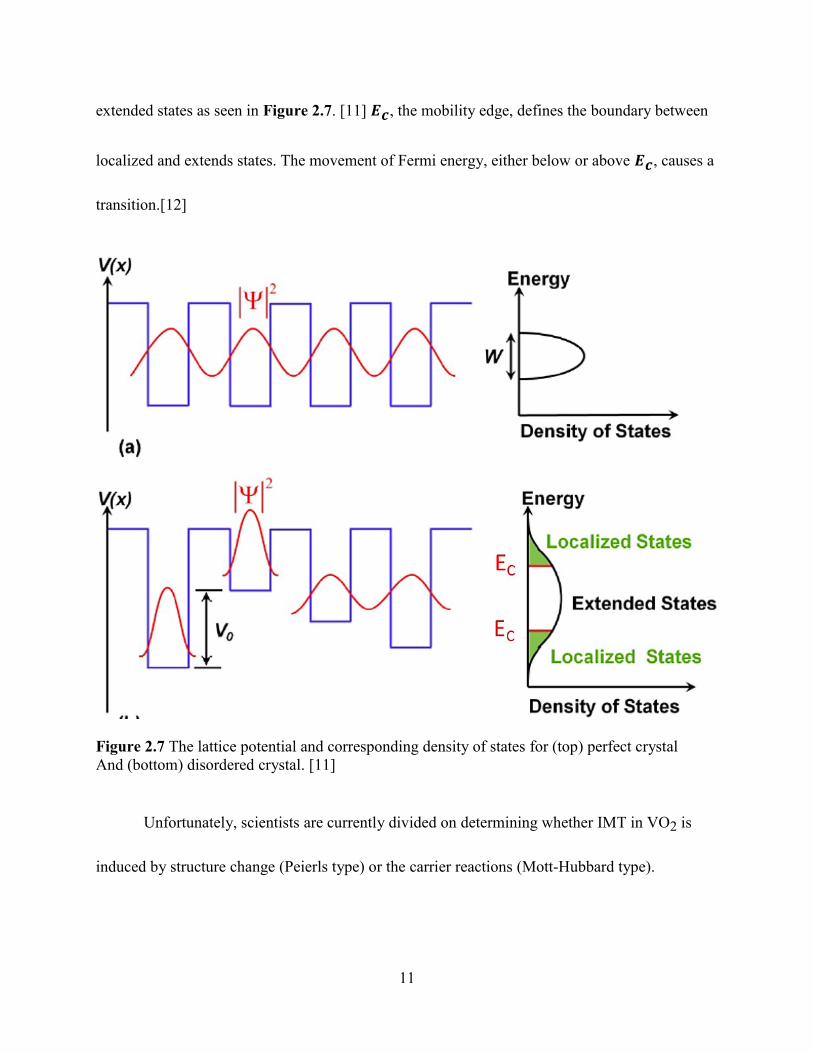
In the third model, Anderson tried to explain IMT using disorder-induced localization
effect. He proposed that randomly distributed defects in a lattice such as impurities or vacancies
can impact conductivity by scattering conducting electrons in the lattice. These defects or
disorders in a system create uneven lattice potentials causing separation of localized and
Page 19
11
extended states as seen in Figure 2.7. [11] , the mobility edge, defines the boundary between
localized and extends states. The movement of Fermi energy, either below or above , causes a
transition.[12]
Figure 2.7 The lattice potential and corresponding density of states for (top) perfect crystal
And (bottom) disordered crystal. [11]
Unfortunately, scientists are currently divided on determining whether IMT in VO2 is
induced by structure change (Peierls type) or the carrier reactions (Mott-Hubbard type).
Page 20
12
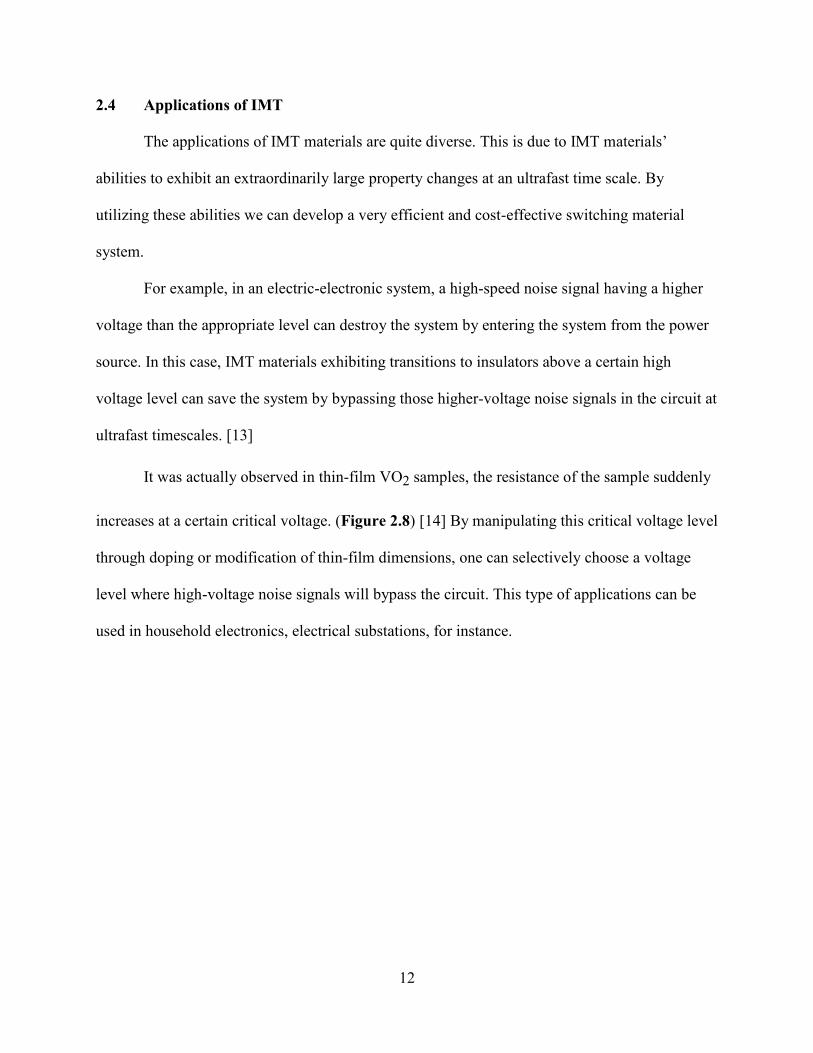
2.4 Applications of IMT
The applications of IMT materials are quite diverse. This is due to IMT materials’
abilities to exhibit an extraordinarily large property changes at an ultrafast time scale. By
utilizing these abilities we can develop a very efficient and cost-effective switching material
system.
For example, in an electric-electronic system, a high-speed noise signal having a higher
voltage than the appropriate level can destroy the system by entering the system from the power
source. In this case, IMT materials exhibiting transitions to insulators above a certain high
voltage level can save the system by bypassing those higher-voltage noise signals in the circuit at
ultrafast timescales. [13]
It was actually observed in thin-film VO2 samples, the resistance of the sample suddenly
increases at a certain critical voltage. (Figure 2.8) [14] By manipulating this critical voltage level
through doping or modification of thin-film dimensions, one can selectively choose a voltage
level where high-voltage noise signals will bypass the circuit. This type of applications can be
used in household electronics, electrical substations, for instance.
Page 21
13
Figure 2.8 I-V curves of thin film VO2 devices. The W indicates thin-film mesa width. (40, 60,
80 and 100 µm were used) The inset shows the critical current fitted for different W values. [14]
Additional promising application can be found in Li-ion batteries. Recently, the explosive
nature of Li-ion batteries, especially those used for cell-phones, has drawn much interest from
the public. In batteries, there is a device called Positive Temperature Coefficient of Resistance
(PTCR) that protects a circuit from short-circuit or overcurrent by blocking the current flow
when the battery is overheated. The electron charges in the blocked current become more
unstable at higher temperatures thereby increasing the internal pressure inside the battery cell.
This will eventually cause the battery to explode.[15]
Page 22
14
In this case, an IMT material can be a good solution. Once the cell phone is overheated,
an IMT-material based explosion prevention device will turn into a metal from an insulator. This
conductive metallic phase will allow the built-up charges inside the battery to be discharged
before explosion. This idea can be applied to laptop batteries as well. [16]
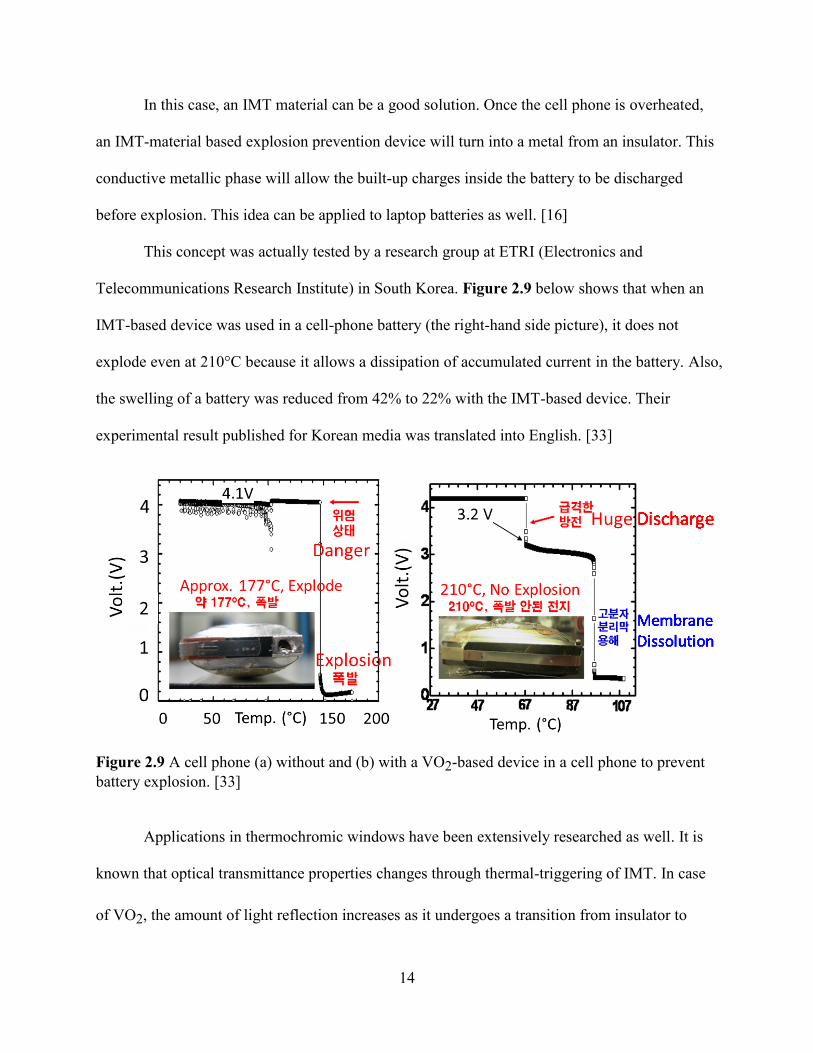
This concept was actually tested by a research group at ETRI (Electronics and
Telecommunications Research Institute) in South Korea. Figure 2.9 below shows that when an
IMT-based device was used in a cell-phone battery (the right-hand side picture), it does not
explode even at 210°C because it allows a dissipation of accumulated current in the battery. Also,
the swelling of a battery was reduced from 42% to 22% with the IMT-based device. Their
experimental result published for Korean media was translated into English. [33]
Figure 2.9 A cell phone (a) without and (b) with a VO2-based device in a cell phone to prevent
battery explosion. [33]
Applications in thermochromic windows have been extensively researched as well. It is
known that optical transmittance properties changes through thermal-triggering of IMT. In case
of VO2, the amount of light reflection increases as it undergoes a transition from insulator to
Page 23
15
metal as seen in Figure 2.3-(a). [7, 8]
Therefore, when the temperature is low as it would be in the winter time, the IMT coating
on glass will allow more light to pass through to maintain warmness in the building. The
situation will be reversed in the summer time when the IMT coating on glass will reflect most of
the light to cool the inside of the building.
It is also important to note that when VO2 changes to a metallic state at a high
temperature, most of the infrared-region (IR) light (longer wavelengths) is reflected as shown in
Figure 2.3-(b). [8] On the other hand, shorter wavelength-light transmittance at a metallic state
remains almost the same through the transition. This special property enables the thermochromic
windows let a sufficient light pass through while selectively blocking infrared radiation-induced
heat at higher temperatures.
2.5 Thermal switching
Thermal switching applications, our work interest, have been investigated hardly at all in
comparison to electronic switching or thermochromic applications. However, a system
dynamically changing its thermal conductivity to the surrounding atmosphere will be an
interesting research subject for its applications in self-regulated heat flow device.
Moreover, since IMT can passively control the heat flow without using thermostats or
specific programs, the power and costs required to operate conventional heat flow directors can
be saved. Thus, this type of thermal switch can be found very useful in an area where power
source is limited. A spacecraft operating with a limited amount of resources in space can be one
example.
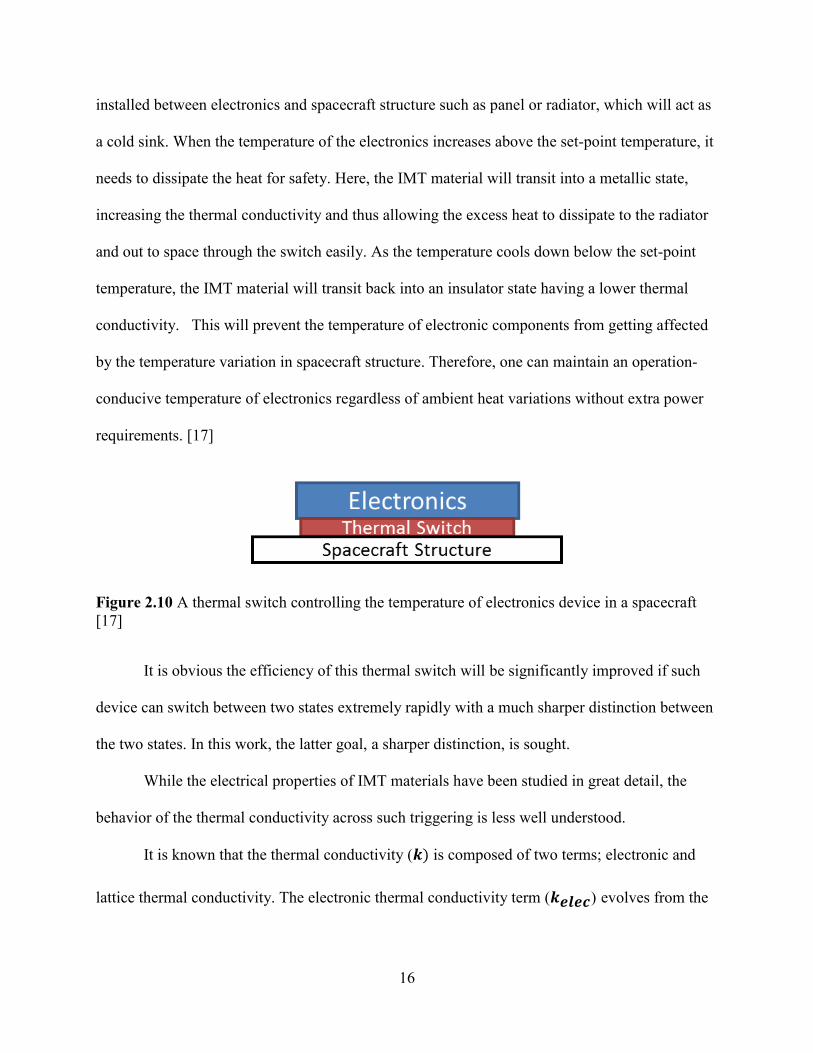
As shown in Figure 2.10 below, a thermal (heat) switch based on IMT material is
Page 24
16
installed between electronics and spacecraft structure such as panel or radiator, which will act as
a cold sink. When the temperature of the electronics increases above the set-point temperature, it
needs to dissipate the heat for safety. Here, the IMT material will transit into a metallic state,
increasing the thermal conductivity and thus allowing the excess heat to dissipate to the radiator
and out to space through the switch easily. As the temperature cools down below the set-point
temperature, the IMT material will transit back into an insulator state having a lower thermal
conductivity. This will prevent the temperature of electronic components from getting affected
by the temperature variation in spacecraft structure. Therefore, one can maintain an operation-
conducive temperature of electronics regardless of ambient heat variations without extra power
requirements. [17]
Figure 2.10 A thermal switch controlling the temperature of electronics device in a spacecraft
[17]
It is obvious the efficiency of this thermal switch will be significantly improved if such
device can switch between two states extremely rapidly with a much sharper distinction between
the two states. In this work, the latter goal, a sharper distinction, is sought.
While the electrical properties of IMT materials have been studied in great detail, the
behavior of the thermal conductivity across such triggering is less well understood.
It is known that the thermal conductivity ( is composed of two terms; electronic and
lattice thermal conductivity. The electronic thermal conductivity term ( ) evolves from the
Page 25
17
electrons carrying not only the charge, but also thermal energy. The lattice thermal conductivity
term ( ) describes heat carried by phonons, quanta of lattice vibrations. The following
equations are generally used to calculate each component.
(2.1)
T (2.2)
(2.3)
where is electrical conductivity, is the Lorenz number, T is the temperature, is the specific
heat per unit volume, is the sound velocity and is the phonon mean free path. [18] Equation
(2.2) relating the electrical and thermal conductivities is known as the Wiedmann-Franz relation.
Since electrons are not free in insulators, the lattice component will be more dominant for
thermal conductivity than the electrical one in insulators. The case is reversed in metals because
there are many free electrons available for conduction.
The key to developing IMT-based thermal switching is to design the material such that
two conditions are achieved: 1) is small throughout the entire temperature range, but
especially below the transition ; and 2) dominates in the metallic state. If these
conditions are met, then as the material passes from the low temperature insulating state to the
high temperature metallic state, the thermal conductivity will transition from small (lattice
dominated) to large (electron dominated).
Page 26
18
2.6 Vanadium dioxide for thermal switching
Among various IMT oxides, VO2 has been a main focus of many scientists because when
it undergoes an IMT, a drastic drop in electrical resistivity or resistance (an order of 104 or 10
5)
occurs at a picosecond time scale as seen in Figure 2.2. The IMT happens approximately at
67 °C for VO2.
This electrical property change is accompanied and driven by with a change in crystal
structure. It has been known that the crystal structure of VO2 changes from monoclinic (insulator
state below TMIT) to tetragonal rutile (metal state above TMIT) during IMT. [10, 19, 20]
Consequently the electronic band structure of VO2 changes as well to reflect a transition from
metal to insulator state. (Figure 2.11)
Figure 2.11 The unit-cell structure of VO2 (left) after and (right) before transition. “MST” stands
for metal to semiconductor transition. [20]
Page 27
19
There have been only a few reports of the behaviors of the thermal conductivity of VO2
across the IMT. Figure 2.12-(a) shows a plot of thermal conductivity vs. temperature for a thin-
film VO2 sample. [21] Figure 2.12-(b) shows the thermal conductivity change through IMT in a
bulk-form VO2 sample analyzed by Berglund in 1969. [22] Here, we can see that the degree of
thermal conductivity change is much lower in a bulk sample than in a thin-film sample.
Moreover, compared to the five orders of magnitude change in resistivity, the magnitude of
change in thermal conductivity needs to be improved for better switching behavior.
Page 28
20
Figure 2.12 A VO2 thermal conductivity, , curve in (a) thin-film (b) bulk form. In (a), the red
triangle-line indicates the values obtained when heating and the black one from cooling. [21,22]
(a)
(b)
Page 29
21
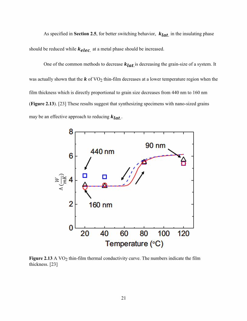
As specified in Section 2.5, for better switching behavior, in the insulating phase
should be reduced while at a metal phase should be increased.
One of the common methods to decrease is decreasing the grain-size of a system. It
was actually shown that the of VO2 thin-film decreases at a lower temperature region when the
film thickness which is directly proportional to grain size decreases from 440 nm to 160 nm
(Figure 2.13). [23] These results suggest that synthesizing specimens with nano-sized grains
may be an effective approach to reducing .
Figure 2.13 A VO2 thin-film thermal conductivity curve. The numbers indicate the film
thickness. [23]
Page 30
22
However, enhancing transition in thermal conductivity is still challenging, and it is
known that a general class of materials exhibits a change in by a factor of ten with a change in
temperature. [35]
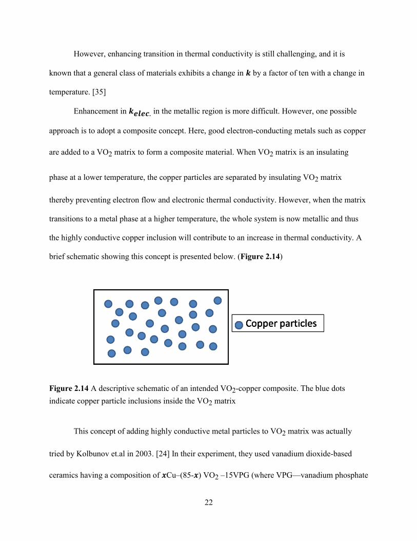
Enhancement in in the metallic region is more difficult. However, one possible
approach is to adopt a composite concept. Here, good electron-conducting metals such as copper
are added to a VO2 matrix to form a composite material. When VO2 matrix is an insulating
phase at a lower temperature, the copper particles are separated by insulating VO2 matrix
thereby preventing electron flow and electronic thermal conductivity. However, when the matrix
transitions to a metal phase at a higher temperature, the whole system is now metallic and thus
the highly conductive copper inclusion will contribute to an increase in thermal conductivity. A
brief schematic showing this concept is presented below. (Figure 2.14)
Figure 2.14 A descriptive schematic of an intended VO2-copper composite. The blue dots
indicate copper particle inclusions inside the VO2 matrix
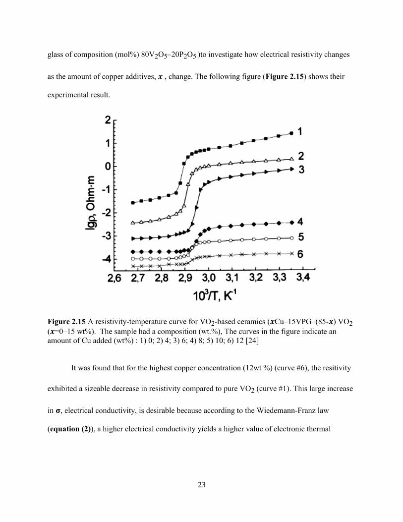
This concept of adding highly conductive metal particles to VO2 matrix was actually
tried by Kolbunov et.al in 2003. [24] In their experiment, they used vanadium dioxide-based
ceramics having a composition of Cu–(85- ) VO2 –15VPG (where VPG—vanadium phosphate
Page 31
23
glass of composition (mol%) 80V2O5–20P2O5 )to investigate how electrical resistivity changes
as the amount of copper additives, , change. The following figure (Figure 2.15) shows their
experimental result.
Figure 2.15 A resistivity-temperature curve for VO2-based ceramics ( Cu–15VPG–(85- ) VO2
( =0–15 wt%). The sample had a composition (wt.%), The curves in the figure indicate an
amount of Cu added (wt%) : 1) 0; 2) 4; 3) 6; 4) 8; 5) 10; 6) 12 [24]
It was found that for the highest copper concentration (12wt %) (curve #6), the resitivity
exhibited a sizeable decrease in resistivity compared to pure VO2 (curve #1). This large increase
in , electrical conductivity, is desirable because according to the Wiedemann-Franz law
(equation (2)), a higher electrical conductivity yields a higher value of electronic thermal
Page 32
24
conductivity. Thus, an increase in due to these conductive metal particles would yield an
increase in at high temperatures.
In designing such composites is, however, care must be taken to ensure that copper
particles are not going to agglomerate in the matrix because this agglomeration could produce
high conductivity even in the low temperature region where we require the material to be
insulating.
2.7 Summary
The switching behavior of IMT materials is potentially very interesting and useful for
modern electronics. Due to their ability to change their electrical properties in the bulk form
significantly at a very small timescale, electronic components, especially transistors, can be
substantially improved in their signal switching ability and power requirement.
More detailed study of the thermal properties, such as thermal conductivity, of IMT
materials may allow the development of a very efficient thermal switching device. Applications
of thermal switches will enable effective control of the temperature automatically without
requiring any additional power resources. This can be useful in spacecraft operations or power
plant operations in which power efficiency is very critical.
For this purpose, VO2 was chosen as a target material in this study because of its rapid
reaction to ambient triggering with an extremely drastic property change. Even though this
drastic change has not been observed in thermal conductivity, , measurement, if we were to
reduce through reduction in grain size and enhance by adopting a carefully
designed highly conductive composite concept , the thermal switching efficiency could be
substantially improved.
Page 33
25
CHAPTER 3. METHODS AND PROCEDURES
Based on information and motivation provided in pervious chapters, we tried to
synthesize a bulk VO2 sample to see whether it can be used as a potential thermal switch. For
this, we first synthesized pure bulk VO2 as a reference, and then conducted ball-milling for
reduction of and synthesized Cu-VO2 composites for enhancement of .
3.1 Synthesizing pure VO2
To synthesize bulk-form pure VO2 samples, hot-pressing, spark plasma sintering (SPS)
and a sol-gel technique were attempted.
i) Materials
(1) Hot Pressing and Spark Plasma Sintering
The 99%-pure metal basis VO2 powder (Product #22957, Alfa Aesar, Ward Hill, MA,
United States) was used for synthesizing a bulk-form VO2. The particle size was -100mesh
and it was stored inside the vacuum glove box to prevent oxidation.
(2) Sol-Gel Technique
For sol-gel technique, 1.2 ml of Vanadium Triisopropoxide oxide (VO[OCH(CH3)2]3) , a
precursor material, (Product #470783, Alfa Aesar, Ward Hill, MA, United States) and a
solvent, composed of 8.6 ml of acetone and 3.6ml of water were prepared.
Page 34
26
i) Procedures
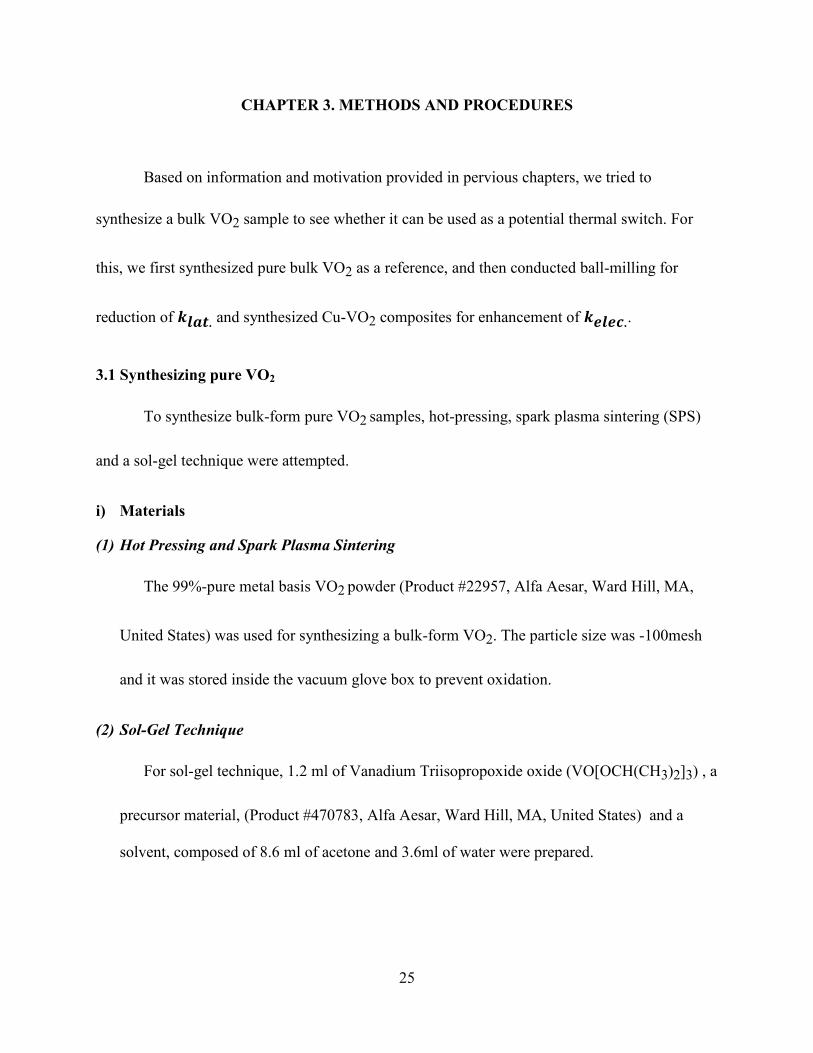
(1) Hot Pressing
The first sintering method used was hot pressing. Here, 2.5 grams of the commercial VO2
powder was pressed into a pellet form under the application of heat and pressure in an inert argon
atmosphere. The sintering temperature was set at 600°C while the pressure level was maintained
at 30MPa. The powder was placed into the graphite die and held under this condition for
approximately 5 minutes. Insulating foam was placed between a heater and the graphite die to
minimize the heat loss.
Subsequently, the system was allowed to cool to ambient. After the sample reached a
room temperature, the ‘puck’ was taken out for further analysis. The descriptive schematic of a
hot press system is presented below. (Figure 3.1)
Figure 3.1 The descriptive schematic of a hot press machine where the heat and pressure is
applied simultaneously to the sample.
Page 35
27
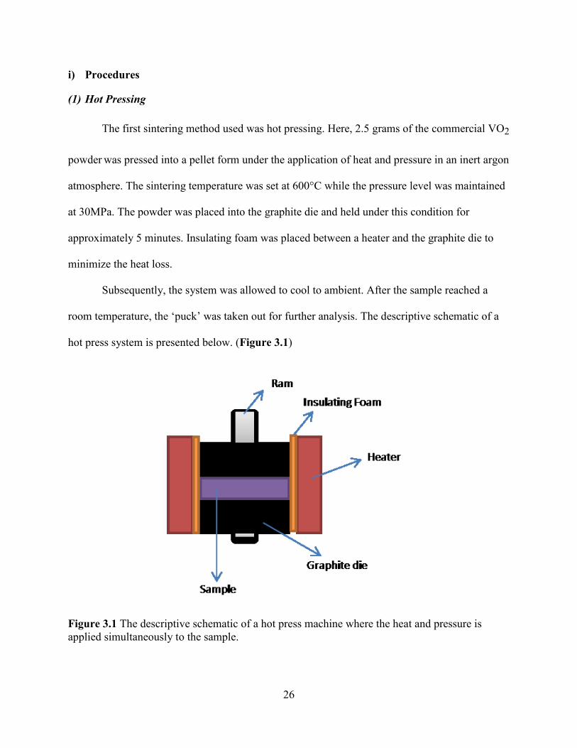
The density of a sample was measured based on Archimedes’ Principle. It states that the
weight of the liquid displaced by an immersed object is equal to the upward force, called
‘buoyancy’, exerting on the object. Based on this, the density of a solid can be measured using a
balance specially set up as shown in Figure 3.2. [34]
Figure 3.2 The descriptive schematic of a density measurement set-up where sample’s weight is
measured in the air and in the liquid.
First, the sample’s weight in the air was measured by placing it on the top pan. Then,
after zeroing out the scale, the sample was placed in the bottom pan immersed in the liquid. The
weight value would be negative. Finally, the following equation was used to measure the density.
| |
where is the density of sample, A is the sample’s weight in the air, B is the weight in liquid and
is the density of liquid. In this experiment, ethanol was used as an immersing liquid. [34]
Following the density measurement, the samples were subjected to XRD to confirm
phase purity. For this, a sample was first ground to a fine powder from using a mortar and a
Page 36
28
pestle. It was then spread on a glass-slide and placed inside an XRD machine (Rigaku MiniFlex
II model). When operating, the machine will collect the intensities of diffracted x-ray beam at
different rotating angles. The resultant scan result was compared to previously established result,
referred to as the PDF-database. If the sample was indeed a single-phase VO2, transport
properties (resistivity, and thermal conductivity, ) were conducted.
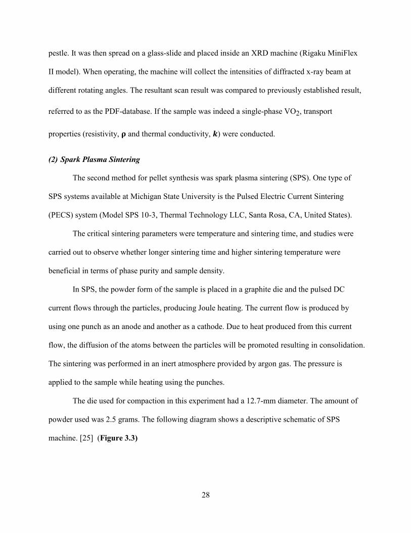
(2) Spark Plasma Sintering
The second method for pellet synthesis was spark plasma sintering (SPS). One type of
SPS systems available at Michigan State University is the Pulsed Electric Current Sintering
(PECS) system (Model SPS 10-3, Thermal Technology LLC, Santa Rosa, CA, United States).
The critical sintering parameters were temperature and sintering time, and studies were
carried out to observe whether longer sintering time and higher sintering temperature were
beneficial in terms of phase purity and sample density.
In SPS, the powder form of the sample is placed in a graphite die and the pulsed DC
current flows through the particles, producing Joule heating. The current flow is produced by
using one punch as an anode and another as a cathode. Due to heat produced from this current
flow, the diffusion of the atoms between the particles will be promoted resulting in consolidation.
The sintering was performed in an inert atmosphere provided by argon gas. The pressure is
applied to the sample while heating using the punches.
The die used for compaction in this experiment had a 12.7-mm diameter. The amount of
powder used was 2.5 grams. The following diagram shows a descriptive schematic of SPS
machine. [25] (Figure 3.3)
Page 37
29
Figure 3.3 The schematic of spark plasma sintering (SPS) where the punches act as electrodes
for current production. [25]
The table below (Table 3.1) summarizes the sintering conditions used in this experiment.
Table 3.1 The temperature and time variations in SPS for pure VO2 synthesis
Parameter Change Temperature (°C) Pressure (MPa) Sintering Time (Min)
Temperature
600 60 5
700 60 5
800 60 5
900 60 5
1000 60 5
Time
900 60 5
900 60 10
900 60 20
900 60 30
900 60 45
900 60 60
Following the density measurement, the samples were subjected to XRD to confirm
phase purity. Only those samples turned out to be a single-phase VO2 from XRD were then
subjected to transport property measurement (resistivity, and thermal conductivity, ).
Page 38
30
(3) Sol-Gel Technique
The vanadium-containing precursor was mixed with a mixture of water / acetone. This
mixture was then chilled with ice for 15 minutes. The gelation occurred rapidly during this
procedure. The obtained gel (xerogel) was composed of V2O5. It was then aged for two days in
the air to enhance densification.
Typically, to release any trapped solvents such as water or acetone out of pores of the
V2O5 gel while retaining its structure, supercritical drying is used to get the trapped solvents out
safely. The final structure without any solvents remaining is called an ‘aerogel’.
However, in this experiment, the first gel sample was dried in the air for a practice run.
After two days, the gel dried in a solid form. This sample was then pulverized to a fine powder
using a mortar and a pestle to be placed in a furnace at a reducing atmosphere (forming gas of 93%
Ar and 7% H). The sample was held at 500 for approximately 10 hours in the furnace,
allowing it to be reduced to VO2.
Following the density measurement, the sample was subjected to XRD to confirm phase
purity. If it turned out to be a single-phase VO2, transport properties (resistivity, and thermal
conductivity, ) were conducted.
(4) High-Energy Ball Milling
To reduce in the insulating region for a better thermal switching behavior, a high-
energy ball milling machine (SPEX Mixer/Mill 8000M model, United States) was used. The
XRD scans of each differently milled sample were analyzed before they were subject to SPS.
For SPS, the sintering temperature was set at 900°C, the pressure at 60MPa and the time for 30
minutes.
Page 39
31
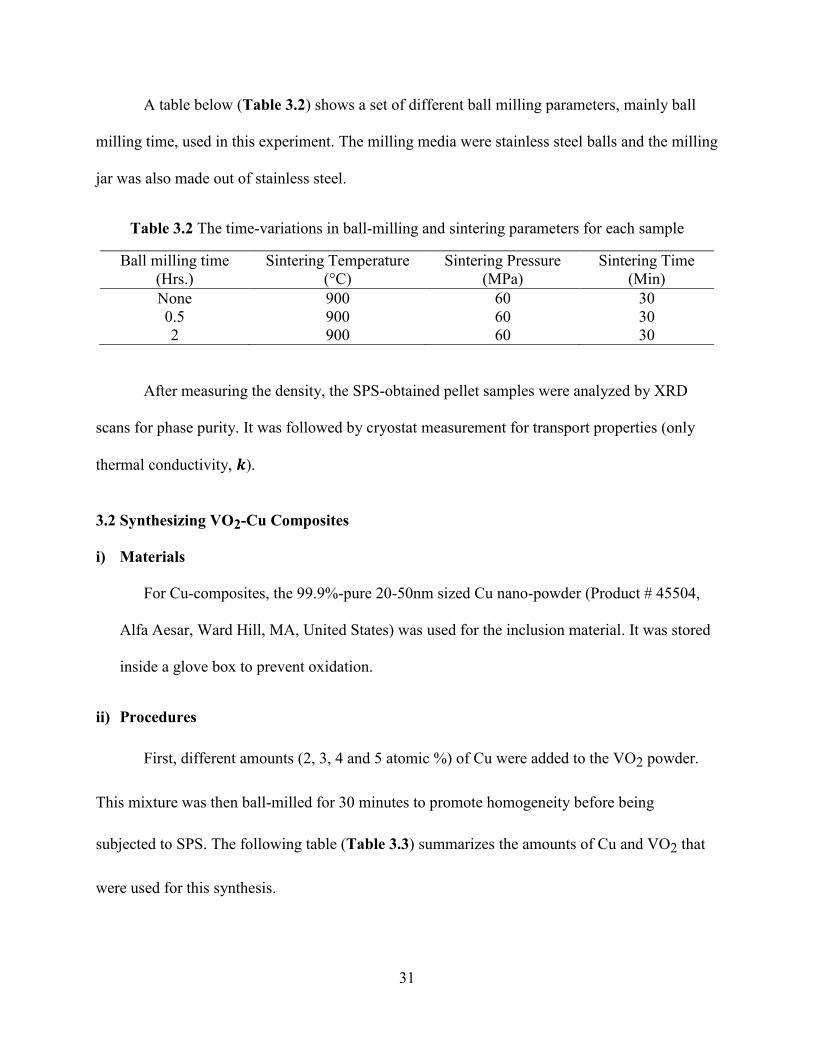
A table below (Table 3.2) shows a set of different ball milling parameters, mainly ball
milling time, used in this experiment. The milling media were stainless steel balls and the milling
jar was also made out of stainless steel.
Table 3.2 The time-variations in ball-milling and sintering parameters for each sample
Ball milling time
(Hrs.)
Sintering Temperature
(°C)
Sintering Pressure
(MPa)
Sintering Time
(Min)
None 900 60 30
0.5 900 60 30
2 900 60 30
After measuring the density, the SPS-obtained pellet samples were analyzed by XRD
scans for phase purity. It was followed by cryostat measurement for transport properties (only
thermal conductivity, ).
3.2 Synthesizing VO2-Cu Composites
i) Materials
For Cu-composites, the 99.9%-pure 20-50nm sized Cu nano-powder (Product # 45504,
Alfa Aesar, Ward Hill, MA, United States) was used for the inclusion material. It was stored
inside a glove box to prevent oxidation.
ii) Procedures
First, different amounts (2, 3, 4 and 5 atomic %) of Cu were added to the VO2 powder.
This mixture was then ball-milled for 30 minutes to promote homogeneity before being
subjected to SPS. The following table (Table 3.3) summarizes the amounts of Cu and VO2 that
were used for this synthesis.
Page 40
32
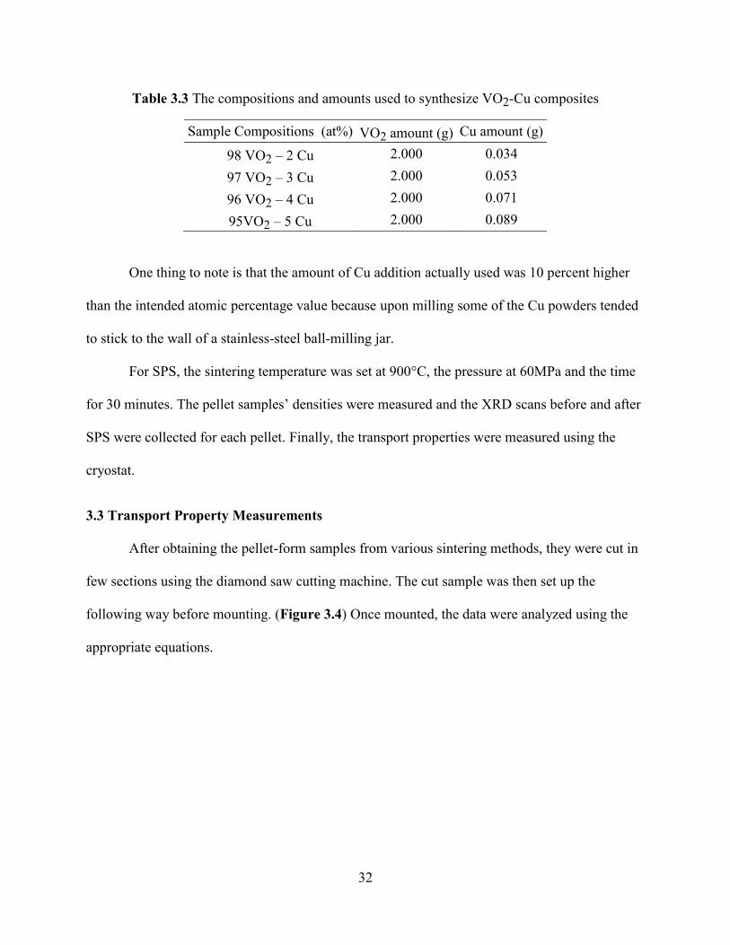
Table 3.3 The compositions and amounts used to synthesize VO2-Cu composites
Sample Compositions (at%) VO2 amount (g) Cu amount (g)
98 VO2 – 2 Cu 2.000 0.034
97 VO2 – 3 Cu 2.000 0.053
96 VO2 – 4 Cu 2.000 0.071
95VO2 – 5 Cu 2.000 0.089
One thing to note is that the amount of Cu addition actually used was 10 percent higher
than the intended atomic percentage value because upon milling some of the Cu powders tended
to stick to the wall of a stainless-steel ball-milling jar.
For SPS, the sintering temperature was set at 900°C, the pressure at 60MPa and the time
for 30 minutes. The pellet samples’ densities were measured and the XRD scans before and after
SPS were collected for each pellet. Finally, the transport properties were measured using the
cryostat.
3.3 Transport Property Measurements
After obtaining the pellet-form samples from various sintering methods, they were cut in
few sections using the diamond saw cutting machine. The cut sample was then set up the
following way before mounting. (Figure 3.4) Once mounted, the data were analyzed using the
appropriate equations.
Page 41
33
Figure 3.4 A set-up diagram for the cryostat sample property measurement where currents are
applied to the sample and heater to measure transport properties and , respectively.
After the sample base temperature is stabilized, current Is is passed through the sample,
and the voltage across the two copper leads of the thermocouple is measured. The electrical
conductivity is determined using Equation 3.1 below.
(3.1)
Page 42
34
The sample current is then turned off, and current Ih is energized through the sample
heater, an 800 resistor on the top of the sample. With this current supply, the heating element
will produce heat based on Joule heating. Due to this heat production, a temperature gradient
will develop throughout the sample (hot and cold sides).
Temperature Thot and Tcold ( T -T are determined by measuring the voltage
across the two thermocouples fixed along the sample. Thermal conductivity, , is then
determined using the following relation. (Equation 3.2)
(3.2)
where , the sample cross-sectional area, , the power, , the length between the probes, , the
heater current, , the heater voltage and is the temperature difference between the two
probes. When analyzing the data, thermal loss caused by radiation was taken into account.
Page 43
35
CHAPTER 4. RESULTS AND DISCUSSION
4.1 VO2 Synthesis
i) Hot Pressed Specimens
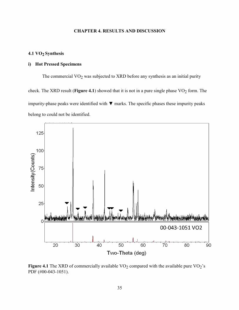
The commercial VO2 was subjected to XRD before any synthesis as an initial purity
check. The XRD result (Figure 4.1) showed that it is not in a pure single phase VO2 form. The
impurity-phase peaks were identified with ▼ marks. The specific phases these impurity peaks
belong to could not be identified.
Figure 4.1 The XRD of commercially available VO2 compared with the available pure VO2’s
PDF (#00-043-1051).
Page 44
36
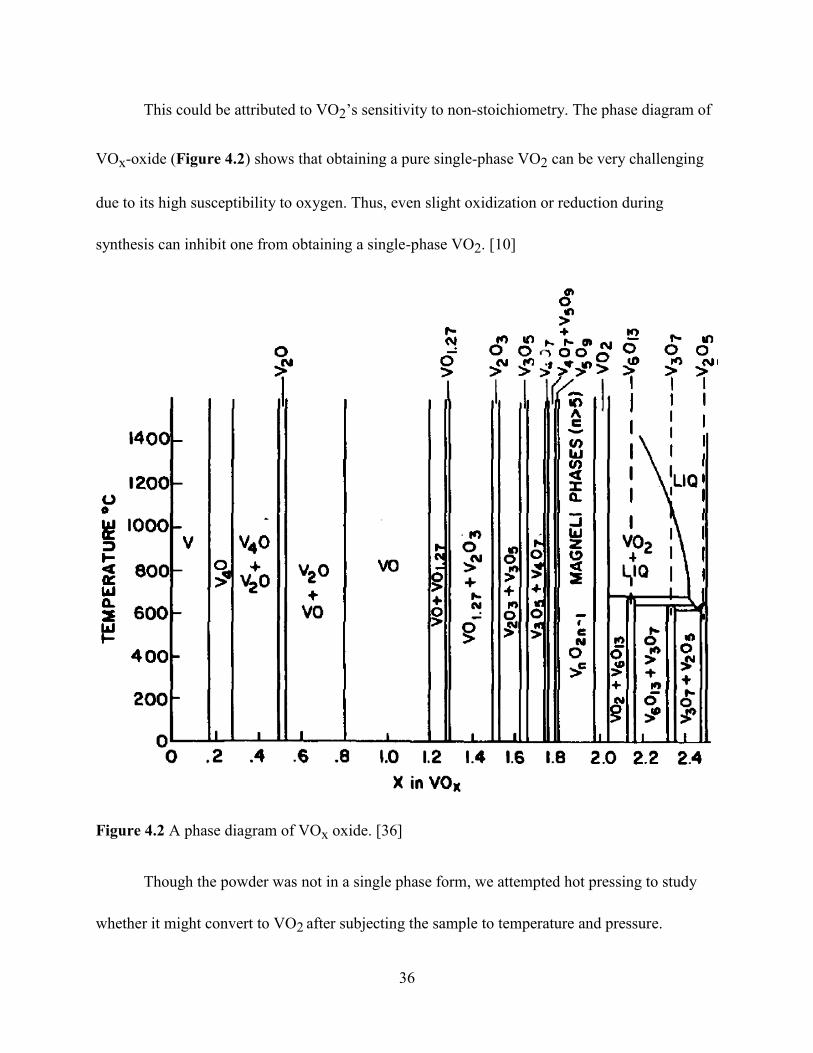
This could be attributed to VO2’s sensitivity to non-stoichiometry. The phase diagram of
VOx-oxide (Figure 4.2) shows that obtaining a pure single-phase VO2 can be very challenging
due to its high susceptibility to oxygen. Thus, even slight oxidization or reduction during
synthesis can inhibit one from obtaining a single-phase VO2. [10]
Figure 4.2 A phase diagram of VOx oxide. [36]
Though the powder was not in a single phase form, we attempted hot pressing to study
whether it might convert to VO2 after subjecting the sample to temperature and pressure.
Page 45
37
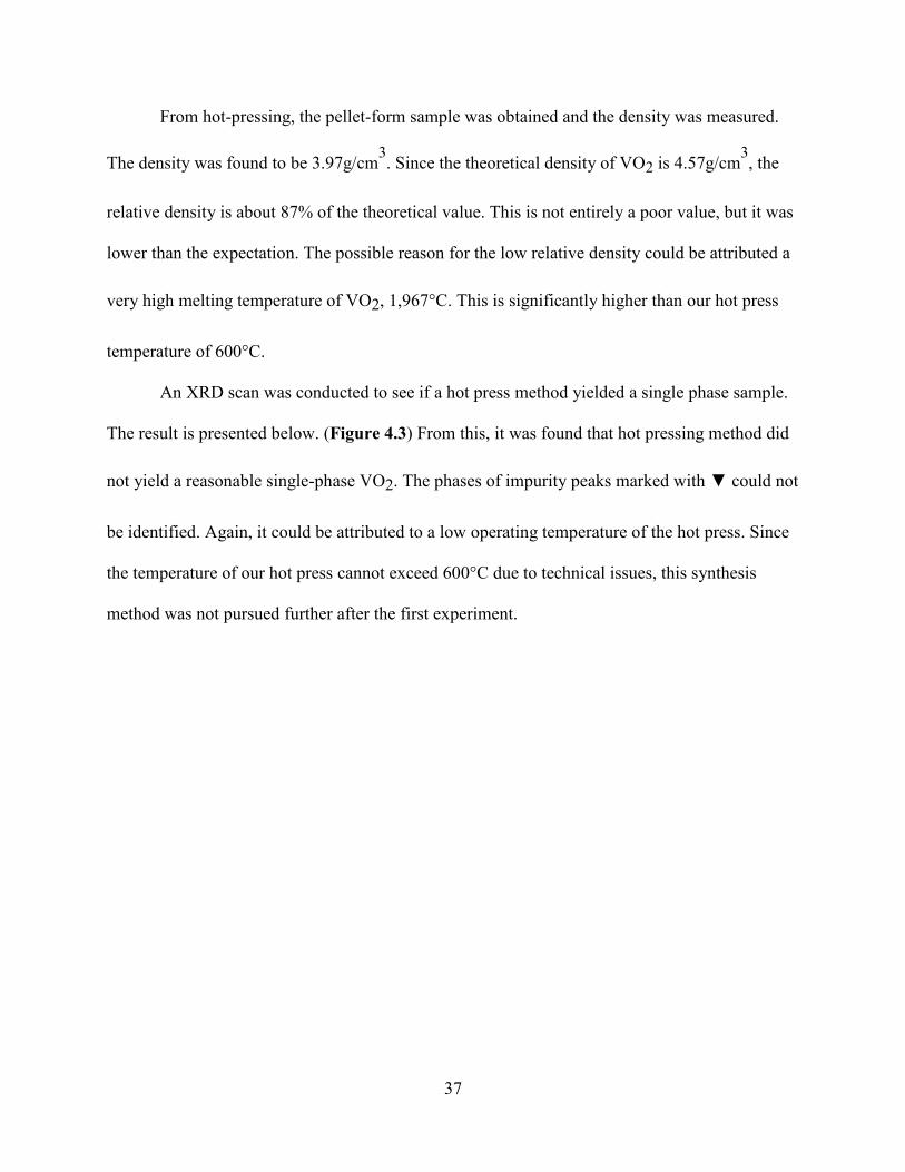
From hot-pressing, the pellet-form sample was obtained and the density was measured.
The density was found to be 3.97g/cm3. Since the theoretical density of VO2 is 4.57g/cm
3, the
relative density is about 87% of the theoretical value. This is not entirely a poor value, but it was
lower than the expectation. The possible reason for the low relative density could be attributed a
very high melting temperature of VO2, 1,967°C. This is significantly higher than our hot press
temperature of 600°C.
An XRD scan was conducted to see if a hot press method yielded a single phase sample.
The result is presented below. (Figure 4.3) From this, it was found that hot pressing method did
not yield a reasonable single-phase VO2. The phases of impurity peaks marked with ▼ could not
be identified. Again, it could be attributed to a low operating temperature of the hot press. Since
the temperature of our hot press cannot exceed 600°C due to technical issues, this synthesis
method was not pursued further after the first experiment.
Page 46
38
Figure 4.3 The XRD scan of a hot-pressed (600°C, 30Mpa for 5 minutes) sample compared to
pure VO2’s PDF
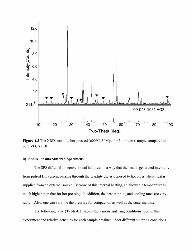
ii) Spark Plasma Sintered Specimens
The SPS differs from conventional hot press in a way that the heat is generated internally
from pulsed DC current passing through the graphite die as opposed to hot press where heat is
supplied from an external source. Because of this internal heating, an allowable temperature is
much higher than that for hot pressing. In addition, the heat ramping and cooling rates are very
rapid. Also, one can vary the die pressure for compaction as well as the sintering time.
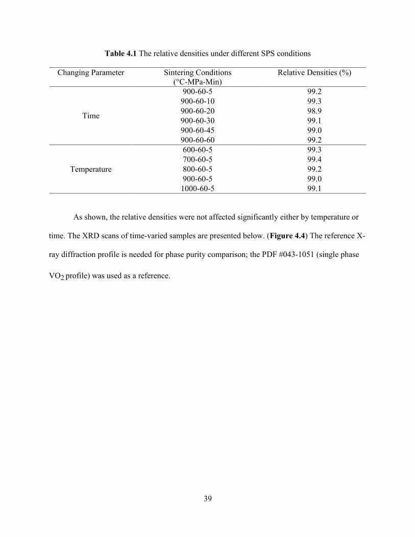
The following table (Table 4.1) shows the various sintering conditions used in this
experiment and relative densities for each sample obtained under different sintering conditions.
Page 47
39
Table 4.1 The relative densities under different SPS conditions
Changing Parameter Sintering Conditions
(°C-MPa-Min)
Relative Densities (%)
Time
900-60-5 99.2
900-60-10 99.3
900-60-20 98.9
900-60-30 99.1
900-60-45 99.0
900-60-60 99.2
Temperature
600-60-5 99.3
700-60-5 99.4
800-60-5 99.2
900-60-5 99.0
1000-60-5 99.1
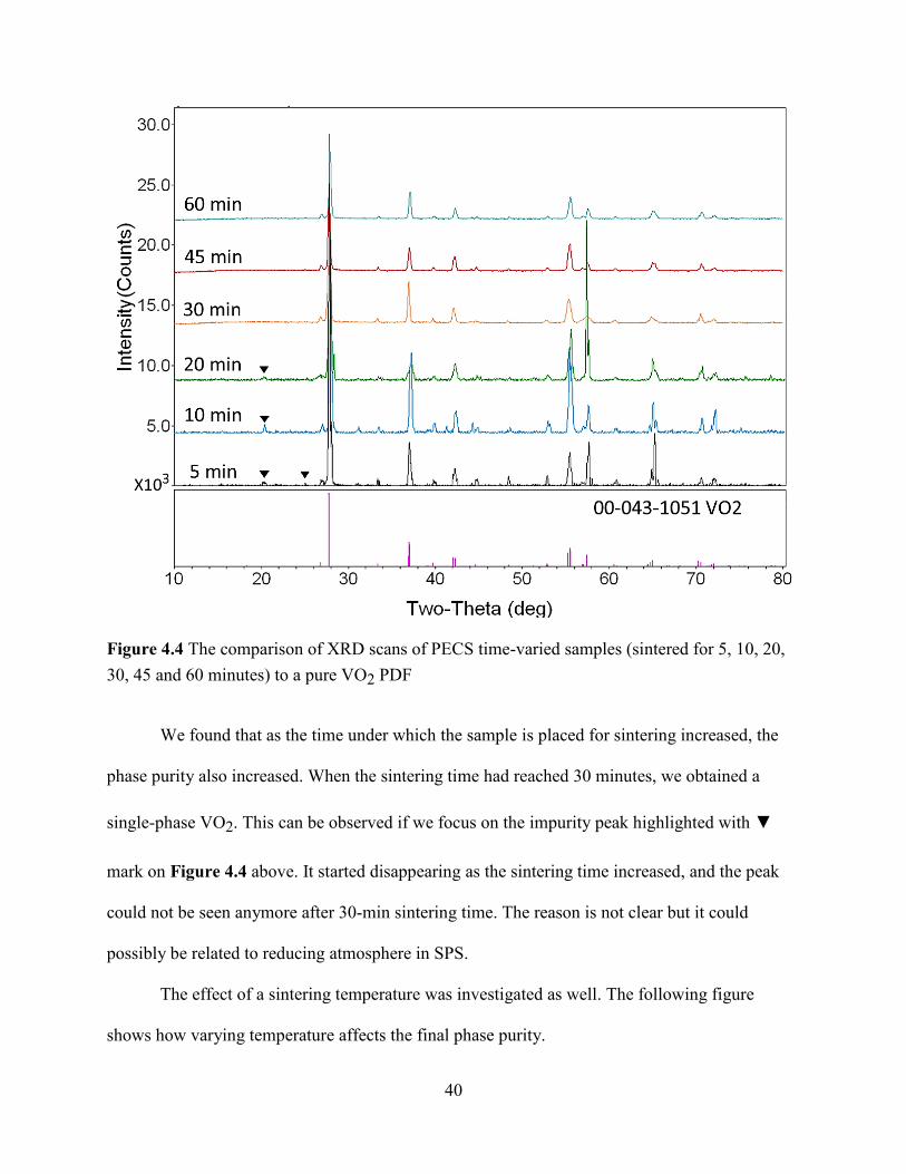
As shown, the relative densities were not affected significantly either by temperature or
time. The XRD scans of time-varied samples are presented below. (Figure 4.4) The reference X-
ray diffraction profile is needed for phase purity comparison; the PDF #043-1051 (single phase
VO2 profile) was used as a reference.
Page 48
40
Figure 4.4 The comparison of XRD scans of PECS time-varied samples (sintered for 5, 10, 20,
30, 45 and 60 minutes) to a pure VO2 PDF
We found that as the time under which the sample is placed for sintering increased, the
phase purity also increased. When the sintering time had reached 30 minutes, we obtained a
single-phase VO2. This can be observed if we focus on the impurity peak highlighted with ▼
mark on Figure 4.4 above. It started disappearing as the sintering time increased, and the peak
could not be seen anymore after 30-min sintering time. The reason is not clear but it could
possibly be related to reducing atmosphere in SPS.
The effect of a sintering temperature was investigated as well. The following figure
shows how varying temperature affects the final phase purity.
Page 49
41
Figure 4.5 The comparison of XRD scans of PECS temperature-varied samples (sintered at 600,
700, 800, 900 and 1000°C) to a pure VO2 PDF. Samples were sintered for 5 minutes.
None of the samples yielded a perfect single-phase even at 1000°C as indicated by ▼
mark for impurity peaks in Figure 4.5 although the highest-temperature sintered sample
(1000°C-sample) showed the least number of impurity peaks. The impurity phases could not be
identified.
Moreover, a higher temperature will produce a larger grain size which in turn will
adversely affect in the insulating region. Thus, for further synthesis, a temperature of
900°C and a 30-minute sintering time would yield the best result.
The transport properties, and , of the single-phase VO2 samples (900°C, 30, 45 and
Page 50
42
60-minute, 60 MPa) were measured using the cryostat. The resistivity data is presented below.
(Figure 4.6) As expected, the resistivity of the sample decreased drastically at the known IMT
temperature, ~340K. The y-axis values were plotted in logarithmic scale. Note the logarithmic
scale on the ordinate axis.
Figure 4.6 The resistivity of 30, 45 and 60-minute sintered samples
With increasing sintering time and temperature, the sample is subject to larger
grain growth. With a larger grain size, there will be less grain-boundary scattering of electrons
when they pass through the lattice. Thus, the lower resistivity in 60-minute sintered sample
compared to the 30 or 45-minute ones seems reasonable. The 30-minute sintered sample has the
highest resistivity, .
The thermal conductivity data for these samples is presented below. (Figure 4.7) The
generally decreases with an increasing temperature except the 30-minute sintered sample which
1.00E-02
1.00E-01
1.00E+00
1.00E+01
1.00E+02
1.00E+03
1.00E+04
1.00E+05
1.00E+06
1.00E+07
1.00E+08
Res
isti
vit
y (
Oh
m-C
m)
Temperature (K)
60min
45min
30min
100 200 300 400
Page 51
43
showed a sudden jump at 200K.
Figure 4.7 The thermal conductivity, , of 30, 45 and 60-minute sintered samples.
This jump is abnormal since it is not the known IMT temperature for VO2; its origin is
unknown and this sample was not studied further. Aside from this unusual behavior, it was seen
clearly that more sintering time indeed led to increase of . The obvious ‘ jump’ at IMT
temperature was not observable, however. This result is congruent with the result Berglund
obtained (Figure 2.12); Berglund claimed that he could not see a distinguishable change in in
a bulk VO2 sample even though he did not know a clear reason behind it.
The 60-minute sample was supposed to have the highest due to the largest grain
crystalline sizes. This was confirmed by our result although all the samples’ converged to
almost the same level past 220K. Thus, we can conclude that the sintering time does not
significantly affect the switching behavior.
0
0.02
0.04
0.06
0.08
0.1
0.12
0 100 200 300 400
Th
erm
al
Con
du
ctiv
ity (
W/m
-K)
Temperature (K)
60min
45min
30min
Page 52
44
iii) Sol-Gel Technique Specimens
Other than using a commercially available VO2, our own synthesis of VO2 powder was
attempted by using a sol-gel technique. The sol-gel method is particularly useful because of its
low-cost, ease of nano-particle formation and ability to dope with various metals. The basic
principle of the sol-gel process is hydrolysis and condensation of precursors, typically metal
alkoxides. [26, 27]
When a sol-gel technique-driven sample was obtained, the color of the sample looked
different than SPS-driven ones. (Figure 4.8) It appeared ‘greener’ than the SPS sample (900°C,
60MPa, 30-minute sintered one selected for comparison).
Figure 4.8 The color difference between the samples obtained from (left) SPS (right) Sol-gel
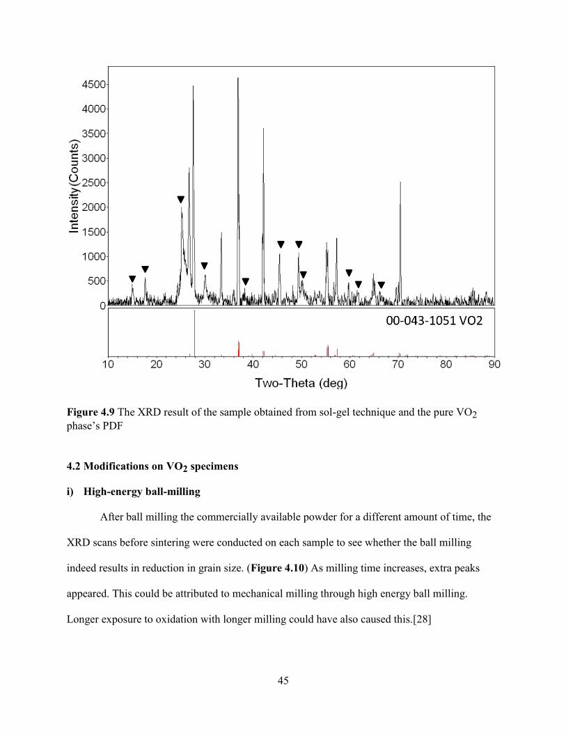
The XRD result confirmed this difference; unlike the SPS sample, the sol-gel sample did
not show a single-phase purity. (Figure 4.9) The impurity peaks (marked with ▼) could not be
identified. Thus, transport property measurement was not conducted.
Page 53
45
Figure 4.9 The XRD result of the sample obtained from sol-gel technique and the pure VO2
phase’s PDF
4.2 Modifications on VO2 specimens
i) High-energy ball-milling
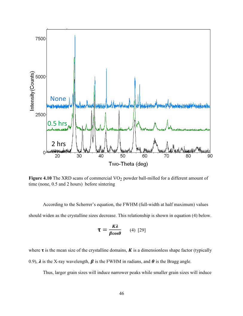
After ball milling the commercially available powder for a different amount of time, the
XRD scans before sintering were conducted on each sample to see whether the ball milling
indeed results in reduction in grain size. (Figure 4.10) As milling time increases, extra peaks
appeared. This could be attributed to mechanical milling through high energy ball milling.
Longer exposure to oxidation with longer milling could have also caused this.[28]
Page 54
46
Figure 4.10 The XRD scans of commercial VO2 powder ball-milled for a different amount of
time (none, 0.5 and 2 hours) before sintering
According to the Scherrer’s equation, the FWHM (full-width at half maximum) values
should widen as the crystalline sizes decrease. This relationship is shown in equation (4) below.
(4) [29]
where is the mean size of the crystalline domains, is a dimensionless shape factor (typically
0.9), is the X-ray wavelength, is the FWHM in radians, and is the Bragg angle.
Thus, larger grain sizes will induce narrower peaks while smaller grain sizes will induce
Page 55
47
broader ones. However, this equation is mostly valid when the sample is nano-sized, and since
we were not sure on our samples’ particle sizes, the effect of ball-milling could only be observed
in transport property measurement.
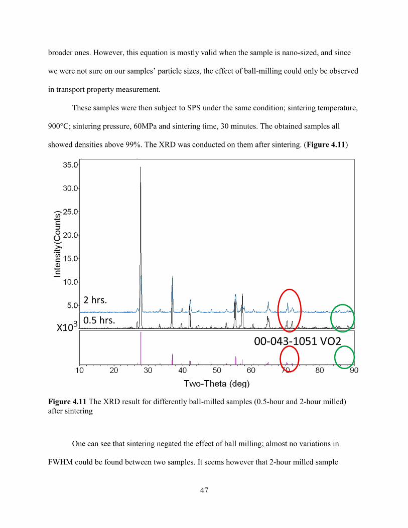
These samples were then subject to SPS under the same condition; sintering temperature,
900°C; sintering pressure, 60MPa and sintering time, 30 minutes. The obtained samples all
showed densities above 99%. The XRD was conducted on them after sintering. (Figure 4.11)
Figure 4.11 The XRD result for differently ball-milled samples (0.5-hour and 2-hour milled)
after sintering
One can see that sintering negated the effect of ball milling; almost no variations in
FWHM could be found between two samples. It seems however that 2-hour milled sample
2 hrs.
0.5 hrs.
Page 56
48
appeared less pure than the 30-minute milled sample. The circled areas in Figure 4.11 show that
the 30-minute milled sample (top curve) corresponds much closer to the available XRD PDF file
than the 2-hour one (bottom curve). This could be due to a longer exposure to oxidation through
ball-milling or more impurity phase produced from mechanical alloying.
However, because the difference was marginal and it still corresponds well to the given
PDF file, we can confirm that 2-hour milled one is also composed of a single-phase VO2.
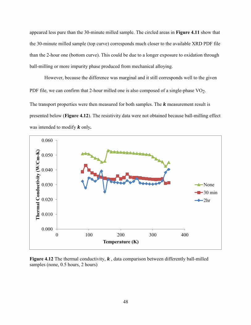
The transport properties were then measured for both samples. The measurement result is
presented below (Figure 4.12). The resistivity data were not obtained because ball-milling effect
was intended to modify only.
Figure 4.12 The thermal conductivity, , data comparison between differently ball-milled
samples (none, 0.5 hours, 2 hours)
0.000
0.010
0.020
0.030
0.040
0.050
0.060
0 100 200 300 400
Th
erm
al
Con
du
ctiv
ity (
W/C
m-K
)
Temperature (K)
None
30 min
2hr
Page 57
49
From equation (3), one can see that reduction of should be witnessed when the
phonon mean free path, , is reduced. Thus, longer ball-milling is supposed to suppress
more than shorter milling. This phenomenon was observed as presented in Figure 4.12 above
where the 2 hour milled sample showed the lowest below the transition temperature while the
non-milled one showed the highest result.
Although the 2 hour-milled sample showed the lowest as intended, the difference
between 30-min milled one and the 2 hour-milled one was marginal. Therefore, 30-min milling
should be enough for reduction in .
The 2 hour milled sample showed the highest switching in through IMT even though
this effect was not expected. Even though this result is meaningful, we cannot entirely trust it
because the XRD result revealed we do not have a pure single-phase VO2 in a 2-hour milled
sample.
ii) VO2-Cu Composites
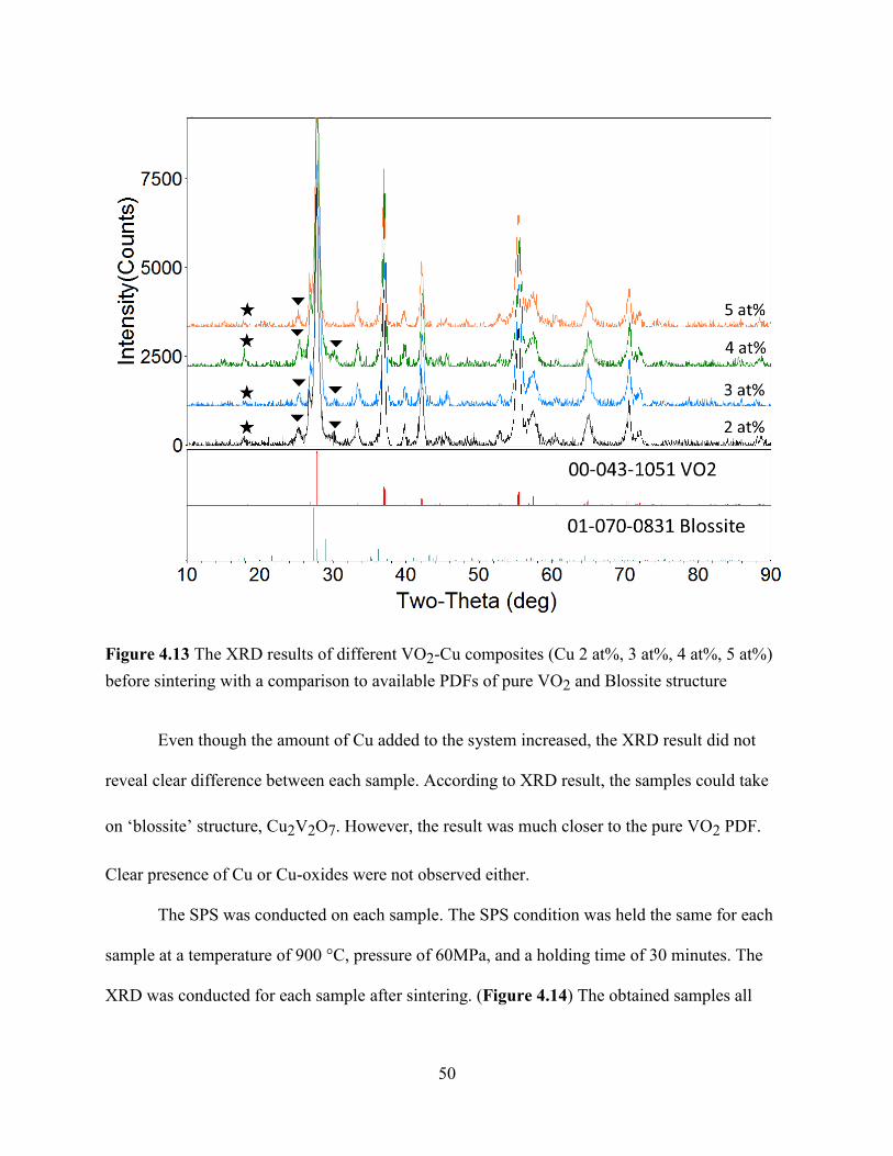
The amount of Cu added to the VO2 system ranges from 2at% to 5at%. The XRD scan
result for each sample before sintering is presented below. (Figure 4.13) The peaks marked with
★ were identified as those belong to Blossite structure, and those marked with ▼ could not be
identified.
Page 58
50
Figure 4.13 The XRD results of different VO2-Cu composites (Cu 2 at%, 3 at%, 4 at%, 5 at%)
before sintering with a comparison to available PDFs of pure VO2 and Blossite structure
Even though the amount of Cu added to the system increased, the XRD result did not
reveal clear difference between each sample. According to XRD result, the samples could take
on ‘blossite’ structure, Cu2V2O7. However, the result was much closer to the pure VO2 PDF.
Clear presence of Cu or Cu-oxides were not observed either.
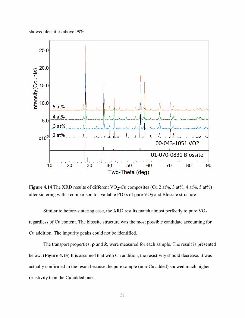
The SPS was conducted on each sample. The SPS condition was held the same for each
sample at a temperature of 900 °C, pressure of 60MPa, and a holding time of 30 minutes. The
XRD was conducted for each sample after sintering. (Figure 4.14) The obtained samples all
Page 59
51
showed densities above 99%.
Figure 4.14 The XRD results of different VO2-Cu composites (Cu 2 at%, 3 at%, 4 at%, 5 at%)
after sintering with a comparison to available PDFs of pure VO2 and Blossite structure
Similar to before-sintering case, the XRD results match almost perfectly to pure VO2
regardless of Cu content. The blossite structure was the most possible candidate accounting for
Cu addition. The impurity peaks could not be identified.
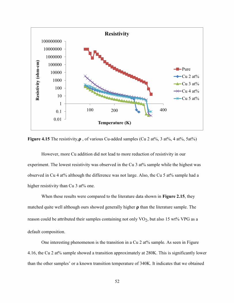
The transport properties, and , were measured for each sample. The result is presented
below. (Figure 4.15) It is assumed that with Cu addition, the resistivity should decrease. It was
actually confirmed in the result because the pure sample (non-Cu added) showed much higher
resistivity than the Cu-added ones.
Page 60
52
Figure 4.15 The resistivity, , of various Cu-added samples (Cu 2 at%, 3 at%, 4 at%, 5at%)
However, more Cu addition did not lead to more reduction of resistivity in our
experiment. The lowest resistivity was observed in the Cu 3 at% sample while the highest was
observed in Cu 4 at% although the difference was not large. Also, the Cu 5 at% sample had a
higher resistivity than Cu 3 at% one.
When these results were compared to the literature data shown in Figure 2.15, they
matched quite well although ours showed generally higher than the literature sample. The
reason could be attributed their samples containing not only VO2, but also 15 wt% VPG as a
default composition.
One interesting phenomenon is the transition in a Cu 2 at% sample. As seen in Figure
4.16, the Cu 2 at% sample showed a transition approximately at 280K. This is significantly lower
than the other samples’ or a known transition temperature of 340K. It indicates that we obtained
0.01
0.1
1
10
100
1000
10000
100000
1000000
10000000
100000000R
esis
tivit
y (
oh
m-c
m)
Temperature (K)
Resistivity
Pure
Cu 2 at%
Cu 3 at%
Cu 4 at%
Cu 5 at%
100 200 400
Page 61
53
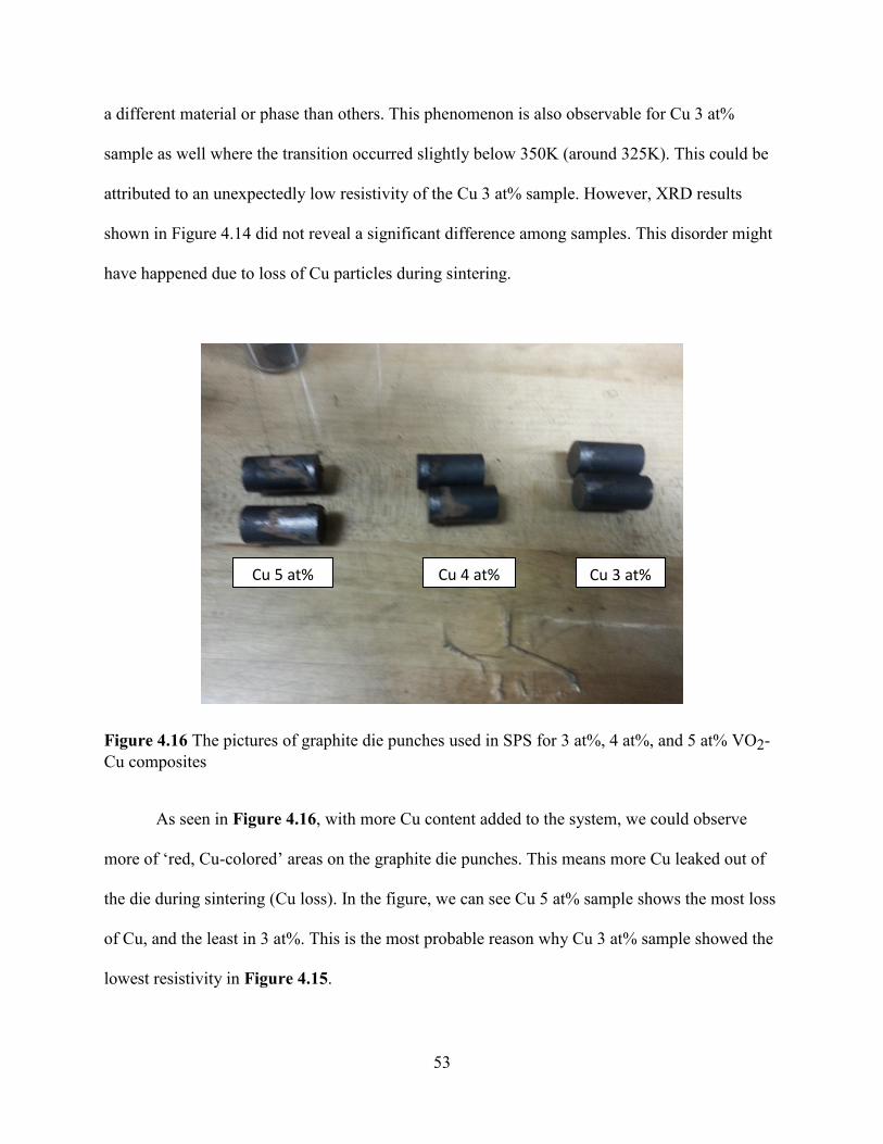
a different material or phase than others. This phenomenon is also observable for Cu 3 at%
sample as well where the transition occurred slightly below 350K (around 325K). This could be
attributed to an unexpectedly low resistivity of the Cu 3 at% sample. However, XRD results
shown in Figure 4.14 did not reveal a significant difference among samples. This disorder might
have happened due to loss of Cu particles during sintering.
Figure 4.16 The pictures of graphite die punches used in SPS for 3 at%, 4 at%, and 5 at% VO2-
Cu composites
As seen in Figure 4.16, with more Cu content added to the system, we could observe
more of ‘red, Cu-colored’ areas on the graphite die punches. This means more Cu leaked out of
the die during sintering (Cu loss). In the figure, we can see Cu 5 at% sample shows the most loss
of Cu, and the least in 3 at%. This is the most probable reason why Cu 3 at% sample showed the
lowest resistivity in Figure 4.15.
Cu 3 at% Cu 4 at% Cu 5 at%
Page 62
54
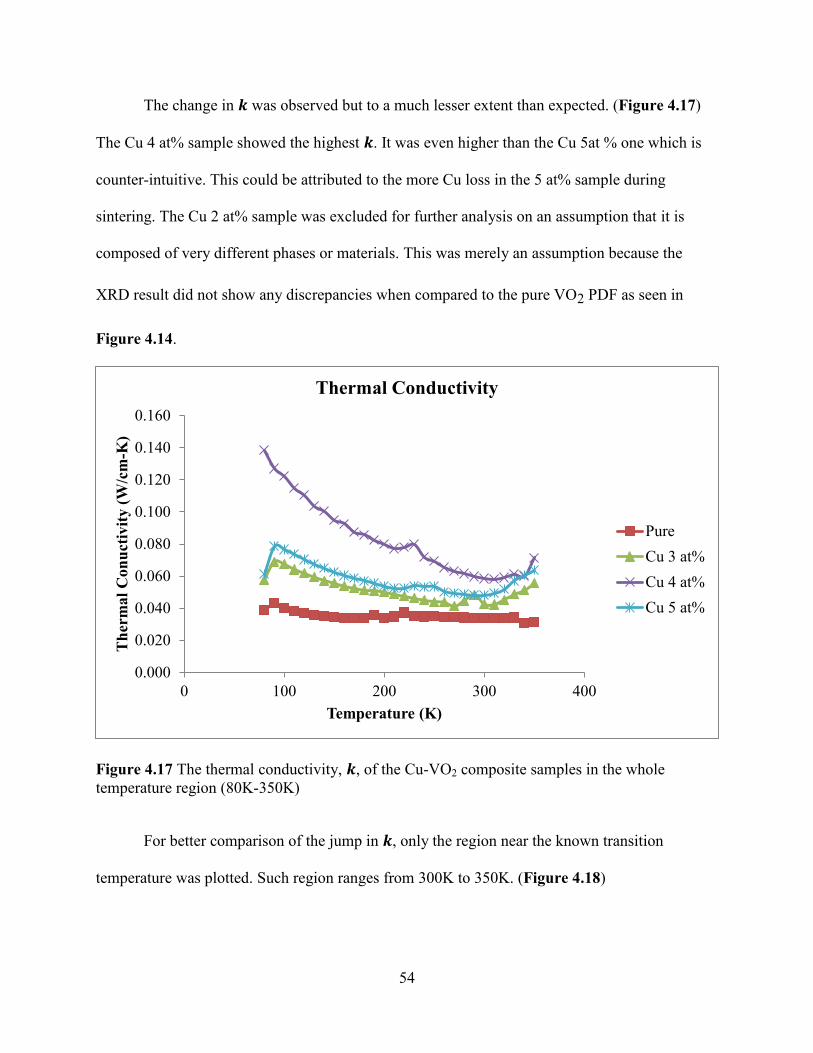
The change in was observed but to a much lesser extent than expected. (Figure 4.17)
The Cu 4 at% sample showed the highest . It was even higher than the Cu 5at % one which is
counter-intuitive. This could be attributed to the more Cu loss in the 5 at% sample during
sintering. The Cu 2 at% sample was excluded for further analysis on an assumption that it is
composed of very different phases or materials. This was merely an assumption because the
XRD result did not show any discrepancies when compared to the pure VO2 PDF as seen in
Figure 4.14.
Figure 4.17 The thermal conductivity, , of the Cu-VO2 composite samples in the whole
temperature region (80K-350K)
For better comparison of the jump in , only the region near the known transition
temperature was plotted. Such region ranges from 300K to 350K. (Figure 4.18)
0.000
0.020
0.040
0.060
0.080
0.100
0.120
0.140
0.160
0 100 200 300 400
Th
erm
al
Con
uct
ivit
y (
W/c
m-K
)
Temperature (K)
Thermal Conductivity
Pure
Cu 3 at%
Cu 4 at%
Cu 5 at%
Page 63
55
Figure 4.18 The thermal conductivity, , of various Cu-added samples in the 300K-350K region
The comparison result is tabulated below. (Table 4.2) It was discovered that Cu 5 at%-
added sample showed the highest change in while the lowest change was seen in the pure
sample. This was the expected result. However, considering the previous observation of the most
Cu loss in the 5% system, it cannot be taken as firm evidence of the influence of Cu. Thus, other
than the Cu loss, the non-uniformity could be a reason. Non-uniformity is not desirable because
only part of the system will experience enhancement in .
Table 4.2 The changes in a 300K-350K region for different VO2-Cu composites
Sample minima
(W/cm-K)
maxima
(W/cm-K)
% change in
(%)
Pure 0.0309 0.0313 1.278
Cu 3 at% 0.0420 0.0550 30.95
Cu 4 at% 0.0580 0.0710 22.41
Cu 5 at% 0.0480 0.0640 33.33
0.000
0.020
0.040
0.060
0.080
0.100
0.120
0.140
0.160
300 310 320 330 340 350
Th
erm
al
Con
uct
ivit
y (
W/c
m-K
)
Temperature (K)
Thermal Conductivity
Pure
Cu 3 at%
Cu 4 at%
Cu 5 at%
Page 64
56
If scanning electron microscopy (SEM) or energy dispersive X-ray spectroscopy (EDS) is
conducted, we could see how Cu particles are distributed in the matrix and thus be able to
explain better why we get higher or lower change in .
Moreover, in Figure 4.17, we can find that the κ still shows an upward trend at 350K, the
maximum reachable temperature in the Cryostat machine. Thus, if we conduct a higher
temperature measurement, we might be able to see more increase in at a higher temperature
region.
Page 65
57
CHAPTER 5. Conclusions
To achieve optimal performance of VO2-based thermal switches, the thermal
conductivity transition should be made much more distinguishable through IMT. This issue
could be addressed with decreasing grain size to lower the lattice thermal conductivity at low
temperatures while using a VO2-metal composite material to increase the electronic thermal
conductivity at high temperatures.
First, synthesizing high purity VO2 bulk samples is crucial. Among various methods,
spark plasma sintering turned out to be the most effective. Although higher temperature and
longer sintering time helps yield a higher purity sample, those parameters will entail large grain
growth, which is adverse for thermal conductivity reduction. Thus, a sintering temperature of
900°C and time of 30 minutes were chosen as a compromise.
For the reduction of lattice thermal conductivity, grain size reduction technique such as
ball-milling was used. It was found that longer ball-milling time leads to a reduction in thermal
conductivity at lower temperatures as expected. The 2-hour ball-milled sample even showed a
better switching behavior although whether this could be reproduced is questionable.
For the enhancement of electronic thermal conductivity, a composite concept was
adopted. A composite of VO2 matrix and highly conductive metal inclusions such as Cu should
give us increase in electronic thermal conductivity after IMT. It was determined that Cu addition
was beneficial for better thermal switching. However, the loss of Cu during sintering should be
taken care of for accurate stoichiometry control. In this experiment, the sample with the highest
Cu concentration showed the best switching behavior as expected.
Page 66
58
CHAPTER 6. FUTURE RESEARCH CONSIDERATIONS
Thermal switches are innovative in a sense that they can control temperatures at a set-
value without requiring additional components or power sources. A better thermal switching
behavior will be achieved if the degree of switching is enhanced greatly.
Therefore, in VO2 system where it is an insulator at a lower temperature and a metal at a
higher temperature, substantial decrease in and increase in will be required.
For more reduction of , a grain growth inhibitor can be used other than ball-milling.
Such inhibitors, for example, can be ZrO2 or Al2O3. These materials are known to inhibit grain
growth during sintering.[30, 31]
Also, organic agent such as oleic acid, OA, is also known to prevent grain agglomeration
during ball-milling. Thus, the addition of OA during ball-milling could be beneficial for lower
. [32]
The can be enhanced more if we use higher thermally conducting materials as
inclusions. The example of the materials having a higher thermal conductivity than copper
includes silver or carbon nanotubes.
The mechanical properties of bulk VO2 need to be improved substantially because all the
bulk samples obtained in this work were too brittle. This will inhibit a wide industrial use. In
addition, finding other IMT materials having better switching behavior and lower cost is also
required.
Page 68
60
BIBLIOGRAPHY
1. Bardeen, J. and W.H. Brattain, The transistor, a semi-conductor triode. Physical Review,
1948. 74(2): p. 230.
2. Perlin, P., et al., Metal-Insulator Transition in GaN Crystals. physica status solidi (b),
1996. 198(1): p. 223-233.
3. Whitten, K.W., Chemistry. 2014, Belmont, CA: Brooks/Cole Cengage Learning.
4. Serway, R.A.J.J.W., Physics for scientists and engineers. Volume 5, Volume 5. 2010,
Pacific Grove, Calif.; Andover: Brooks/Cole ; Cengage Learning [distributor].
5. Zhang, R.-z., et al., Thermoelectric transport coefficients of n-doped CaTiO3, SrTiO3
and BaTiO3: A theoretical study. Physica B: Condensed Matter, 2012. 407(7): p. 1114-
1118.
6. Chandra, S., Comprehensive inorganic chemistry (for B.Sc 1st year). 2004, New Delhi,
India: New Age International (P) Ltd. Pub.
7. Nag, J. and R. Haglund Jr, Synthesis of vanadium dioxide thin films and nanoparticles.
Journal of Physics: Condensed Matter, 2008. 20(26): p. 264016.
8. Maaza, M., et al., Direct production of thermochromic VO2 thin film coatings by pulsed
laser ablation. Optical Materials, 2000. 15(1): p. 41-45.
9. Si, C., et al., Metal-insulator transition in V(1-x)W(x)O2: structural and electronic origin.
Phys Chem Chem Phys, 2012. 14(43): p. 15021-8.
10. Yang, Z., C. Ko, and S. Ramanathan, Oxide electronics utilizing ultrafast metal-insulator
transitions. Annual Review of Materials Research, 2011. 41: p. 337-367.
11. Zhou, Y. and S. Ramanathan, Correlated Electron Materials and Field Effect Transistors
for Logic: A Review. arXiv preprint arXiv:1212.2684, 2012.
12. Dorokhov, O.N., On the coexistence of localized and extended electronic states in the
metallic phase. Solid State Communications, 1984. 51(6): p. 381-384.
13. Kim, H.T., et al., Abrupt metal-insulator transition device, circuit for removing high-
voltage noise using the abrupt metal-insulator transition device, and electrical and/or
electronic system comprising the circuit, 2009, European Patent # EP 1911137 A1
14. Yong, Z., et al., Electrically controlled metal–insulator transition process in VO 2 thin
films. Journal of Physics: Condensed Matter, 2012. 24(3): p. 035601.
Page 69
61
15. Feng, X.M., X.P. Ai, and H.X. Yang, A positive-temperature-coefficient electrode with
thermal cut-off mechanism for use in rechargeable lithium batteries. Electrochemistry
Communications, 2004. 6(10): p. 1021-1024.
16. Bush, C.H., Thermal switch for battery protection, 1991,U.S Patnet # US5070427.
17. Gilmore, D.G., Spacecraft thermal control handbook Vol. 1 Vol. 1. 2002, El Segundo,
Calif: Aerospace Press [u.a.].
18. Ho, C.Y., et al., Thermal conductivity of ten selected binary alloy systems. Journal of
Physical and Chemical Reference Data, 1978. 7(3): p. 959-1178.
19. Griffiths, C.H. and H.K. Eastwood, Influence of stoichiometry on the metal-
semiconductor transition in vanadium dioxide. Journal of Applied Physics, 1974. 45(5): p.
2201-2206.
20. Li, Y., et al., Core-shell VO2@TiO2 nanorods that combine thermochromic and
photocatalytic properties for application as energy-saving smart coatings. Sci Rep, 2013.
3: p. 1370.
21. Zhang, Y. and S. Ramanathan, Analysis of “on” and “off” times for thermally driven
VO2 metal-insulator transition nanoscale switching devices. Solid-State Electronics,
2011. 62(1): p. 161-164.
22. Berglund, C. and H. Guggenheim, Electronic Properties of VO_ {2} near the
Semiconductor-Metal Transition. Physical Review, 1969. 185(3): p. 1022.
23. Oh, D.-W., et al., Thermal conductivity and dynamic heat capacity across the metal-
insulator transition in thin film< equation>< font face='verdana'> VO</font>< sub>
2</sub></equation>. Applied Physics Letters, 2010. 96(15): p. 151906-151906-3.
24. Kolbunov, V., A. Ivon, and I. Chernenko, Influence of a high conductivity additive on the
electrical properties of vanadium dioxide-based ceramics. Journal of the European
Ceramic Society, 2003. 23(9): p. 1435-1439.
25. O’Brien, R.C., et al., Spark Plasma Sintering of simulated radioisotope materials within
tungsten cermets. Journal of Nuclear Materials, 2009. 393(1): p. 108-113.
26. Siciliano, P., Preparation, characterisation and applications of thin films for gas sensors
prepared by cheap chemical method. Sensors and Actuators B: Chemical, 2000. 70(1–3):
p. 153-164.
27. Brinker, C.J.S.G.W., Sol gel science : the physics and chemistry of sol-gel processing.
1993, Boston [u.a.]: Acad. Press.
Page 70
62
28. Calka, A. and A.P. Radlinski, Universal high performance ball-milling device and its
application for mechanical alloying. Materials Science and Engineering: A, 1991. 134(0):
p. 1350-1353.
29. Monshi, A., Modified Scherrer Equation to Estimate More Accurately Nano-Crystallite
Size Using XRD. World Journal of Nano Science and Engineering, 2012. 02(03): p. 154-
160.
30. Fisher, J.G., et al., Inhibition of abnormal grain growth in BaTiO3 by addition of Al2O3.
Journal of the European Ceramic Society, 2006. 26(9): p. 1619-1628.
31. Lange, F.F. and M.M. Hirlinger, Hindrance of Grain Growth in Al2O3 by ZrO2
Inclusions. Journal of the American Ceramic Society, 1984. 67(3): p. 164-168.
32. Zhang, Q., et al., Suppression of grain growth by additive in nanostructured p-type
bismuth antimony tellurides. Nano Energy, 2012. 1(1): p. 183-189.
33. Electronics and Telecommunications Research Institute (ETRI), South Korea, "Report
Data for Media (2006-76) / ETRI, MIT원리 적용 임계온도 스위치 개발성공 - 휴대폰,
노트북 배터리 부풀림 및 폭발방지 적용가능" (ETRI, MIT mechansim applied-ciritcal
temperature thremal switch devleopment success - Applications in cell phone, laptop
battery swell and explosion prevention). The Korean version can be obtained at
"http://www.etri.re.kr/etri/pro/pro_01010000.etri?type=view&b_idx=2182"
34. A&D Company Limited, GX-13 Density Determination Kit For GX-200/400/600
Instruction Manual, can be obtained at www.aandd.jp/products/manual/balances/gx-
13.pdf
35. S.M Marcus and R.L. Blaine, Thermal Conductivity of Polymers, Glasses & Ceramics by
Modulated DSC, Thermochimica Acta 243.2 (1994) : 231-239
36. Griffith C H and Eastwood H K 1974 Influence of stoichiometry on metal.semiconductor
transition in vanadium dioxide J. Appl. Phys. 45 2201.6