37
www.123vfd.com 1-800-916-4272 VFDA revision 1.1b Specifications subject to change without notice VFDA Patent Pending. Copyright 2008. Page 1 of 37 Variable Frequency Drive Analyzer

www.123vfd.com 1-800-916-4272 VFDA revision 1.1b
Specifications subject to change without notice VFDA Patent Pending. Copyright 2008. Page 1 of 37
Variable Frequency Drive Analyzer

www.123vfd.com 1-800-916-4272 VFDA revision 1.1b
Specifications subject to change without notice VFDA Patent Pending. Copyright 2008. Page 2 of 37
Table of Contents Variable Frequency Drive Analyzer....................................................................................1 Table of Contents.................................................................................................................2 WARNING..........................................................................................................................3 Product Summary ................................................................................................................4 Product Cautions and Theory of Operation.........................................................................5 Basic Product Operation......................................................................................................6 Standard Safety Practices ....................................................................................................6 Display Notation..................................................................................................................6 Variable Frequency Drive Troubleshooting Tutorial ..........................................................7 VFD Tutorial Rectifier Circuit (Stage 1 of VFD) ...............................................................9 VFD Tutorial Fix DC Voltage (Stage 2 of VFD) ..............................................................12 VFD Tutorial Inverter Circuit (Stage 3 of VFD) ...............................................................15 VFD Tutorial Verification of Bad Rectifier ......................................................................20 VFD Tutorial Verification of Bad Capacitor .....................................................................23 VFD Tutorial Verification of Bad Transistor Module.......................................................24 VFD Tutorial Other Components ......................................................................................27 Transistor / Thyristor Test .................................................................................................28 Capacitance and Resistance Testing ..................................................................................32 Diode Testing.....................................................................................................................34 Troubleshooting .................................................................................................................37
www.123vfd.com 1-800-916-4272 VFDA revision 1.1b
Specifications subject to change without notice VFDA Patent Pending. Copyright 2008. Page 3 of 37
WARNING Proceed no further with this manual or attempt connecting the VFD Analyzer to an actual electronic device unless you are sufficiently trained and familiar with all practical safety standards regarding high voltage electronic circuits. Deadly voltages exist in these devices and you must be aware of the presence of these hazardous potentials and how to monitor, measure, and neutralize them before operating the equipment. The manufacturer makes no representation to direct, inform or instruct the safe operation of the VFD Analyzer in regards to a specific piece of High Voltage electronic equipment. The manufacturer will not be held liable for equipment damage or personal injury as a result of following the directions suggested within this document. The suggestions contained herein are by no means the only or sole suggestions that represent completely safe and damage free use or operation of the equipment. It is up to the user to determine what methods and practices are most suitable for their particular scenario. Wear protective head gear including safety glasses, shields and body protection as well as hearing protection when troubleshooting VF Drives and other types of conversion equipment. High Power devices including solid state modules and capacitors can explode causing fragments and hot gases to escape the confines of the equipment.

www.123vfd.com 1-800-916-4272 VFDA revision 1.1b
Specifications subject to change without notice VFDA Patent Pending. Copyright 2008. Page 4 of 37
Product Summary The Variable Frequency Drive Analyzer (VFDA) is a multipurpose testing instrument, and is designed specifically to analyze the components in-circuit of the increasingly popular Variable Frequency Drives (VFD) for AC Motor control. The VFDA can test many other semiconductor and passive electronic components in addition to identifying faulty VFD components. Each of the three settings on the VFDA targets each of the three main stages of a VFD.
Figure 1
The last stage of the VFD, the Inverter Circuit, takes the DC energy stored and produces the AC voltage needed to turn the motor. All of the semiconductors (IGBT, FET, SCR, etc) in this stage have very similar properties to each other. As one fails, or even simply starts to fail, those properties are no longer a similar enough to drive the motor properly. With the push of a button, the VFDA will characterize current and voltage properties of the connected component and then display the results on the LCD. After doing the same for the second VFD component, the press of another button will allow quick comparison between the two tests, allowing rapid identification of the failing or failed component while still in-circuit. The previous stage of the VFD stores the rectified AC power as DC power for the output stage. If the capacitors have failed and no longer hold a charge, or the bleed resistor has failed causing a safety concern for technicians, the VFDA will identify the problem. The VFDA will report the in-circuit measured capacitance, resistance, and RC time constant.

www.123vfd.com 1-800-916-4272 VFDA revision 1.1b
Specifications subject to change without notice VFDA Patent Pending. Copyright 2008. Page 5 of 37
The first stage of a VFD takes incoming Alternating Current (AC) and rectifies it to Direct Current (DC) for storage. If any of the diodes in this stage fail, insufficient power will be available to run the motor. Connect the probes to the diodes for a given phase, and the VFDA will display the test results for both. After testing the next set of diodes, another button press allows quick comparison to the first two diodes; any significant differences which would affect performance are quickly identified. In circuit testing is difficult for standard multimeters due to the affect of other components in the circuit, but the VFDA minimizes these affects to isolate the problem without having to remove each component individually. The VFDA allows testing of diodes in-circuit with large capacitance that would hinder standard meters. The VFDA can often even help differentiate the type of semi-conductor in-circuit, displaying the results on screen, Insulated Gate Bipolar Transistors (IGBT) or N Channel Field Effect Transistor (NFET), NPN Bipolar Junction Transistor (BJT), PNP BJT, PFET, and Silicon Controlled Rectifier (SCR) or Triode AC Switch (Triac). Knowing the pinout of the 3 pin semiconductor is not necessary; clip on the three probes on the three pins in any order and the VFDA will display the pinout on screen. The components need not be in-circuit for testing, and can be tested again after removal from circuit to verify the results.
Product Cautions and Theory of Operation This product operates by producing large current pulses (200mA to 400mA) at up to 12 volts for very brief moments followed by a significant period of inactivity. The large currents and voltage are necessary to fully test the components of VFDs, and the significant periods of inactivity are used to minimize component heating. Do NOT use the VFDA on very sensitive electronic circuits since damage may result. Standard multimeters use low voltage and low current in testing. Do NOT use on circuits or components that should not be exposed to 12V such as low voltage capacitors or semi-conductors. Many components are capable of surviving these brief pulses, and even many small TO-92 transistors have been tested successfully without component damage. A main source of semi-conductor damage is overheating, which the VFDA attempts to minimize by significant length of time between short pulses of energy. Do not connect the VFDA to voltage sources, as this will likely result in blowing the internal VFDA fuses. Disconnect power from and discharge all circuits prior to connecting the VFDA probes.

www.123vfd.com 1-800-916-4272 VFDA revision 1.1b
Specifications subject to change without notice VFDA Patent Pending. Copyright 2008. Page 6 of 37
Basic Product Operation The VDFA operation is much like a standard multimeter. First connect the probes to the component to be tested. Then turn the rotary switch on to the desired component to test. The VFDA tests the component, and then displays the results. Press the NEXT RESULT button to rapidly scroll through test results. Move the probes to the next similar component and press the START TEST button to run the test again. After testing a second similar component, the resulting data can be displayed in percentages of the previous test results instead of in volts and mA by pressing the COMPARE LAST button; this allows quick comparison through multiple parts.
Standard Safety Practices Always follow all safety practices when working with components that deal with high voltage. Disconnect power, use tag out procedures, remove fuses, and/or any other necessary actions. Always allow necessary time for capacitors with high voltage to discharge and/or discharge them manually. Always probe for voltage on a circuit, and never assume equipment is safe without checking. The VFDA is NOT designed to measure voltage sources. Always disconnect power to equipment prior to connecting the VFDA. Do not connect the VFDA to buses that are charged with DC voltage; always use safe practices to measure and discharge residual voltage charge. Warning: For the protection of equipment under test and the VFDA, connecting the VFDA to a voltage source over 12 volts may blow the VFDA internal fuses.
Display Notation Different semiconductor types have different names for their pins for historical and technical reasons, but they serve a very similar purpose so for analytical purposes we can consider them the same. The IGBT, for example, allows control of the voltage across and the current through the Collector to the Emitter by changing the voltage on the Gate with reference to the Emitter. The VFDA displays the voltages and currents using the notations “Vce” as the voltage measured across the Collector to the Emitter, and “Ig” as the current measured passing into the Gate. With NFETs, the controlling pin is still called a “Gate”, but the other two pins are called the Drain and the Source. Just like the controlled current flows into the Collector and out of the Emitter in the IGBT, the current also flows into the Drain and out of the Source in the NFET. Therefore, the same “Ic” on the VFDA display is used to denote the controlled current flowing into the component regardless of the type of component. The SCR or Triac similar has current flow into the Anode and out of the Cathode, but Vce and Ic will still be displayed. The BJT controlling pin is called as Base and not a Gate, but the VFDA will display “Vge” for the voltage measured across the Base to the Emitter for a tested BJT semiconductor.

www.123vfd.com 1-800-916-4272 VFDA revision 1.1b
Specifications subject to change without notice VFDA Patent Pending. Copyright 2008. Page 7 of 37
Variable Frequency Drive Troubleshooting Tutorial Figure 2: Variable Frequency Drive
Welcome to the VFD Troubleshooting Tutorial. This guide will help you step through the processes of troubleshooting a VFD. Please note, every VFD will be different; different housings, components, locations, terminals, specifications, etc so your VFD may not look exactly like this, but should contain all of the basic elements shown in Figure 1 above. This guide will step through locating each of those components and testing them with the VFDA. These common components are common failure points. This VFD is shown without external wiring; removing the wiring is not required, but power to the VFD MUST be disconnected prior to using the VFDA. Always follow safe power down and tag out procedures before servicing.
Figure 3: VFD Cover Removed First remove the cover. This VFD had only plastic tabs; once pressed inward, the cover easily lifts off. Other VFDs may have screws holding the cover in place that may first have to be removed. DO NOT TOUCH any conductive surfaces ( screws, solder joints, bare wires) without checking for voltage with a standard multimeter, especially if external wiring is still connected. VFDs contain large capacitors that can hold a large voltage charge for a considerable length of time. If charge is found discharge through safe methods, possibly with the use of an external resistor of sufficient rating. An exception would be low voltage batteries used to keep memory powered need not be discharged for service.

www.123vfd.com 1-800-916-4272 VFDA revision 1.1b
Specifications subject to change without notice VFDA Patent Pending. Copyright 2008. Page 8 of 37
Figure 4: Electronics PCB
Next loosen and set aside any screws holding the main electronics board in place. Every VFD has complex electronic circuits that monitor and control the main components shown in Figure 1, but this electronics board (shown in Figure 3) is less often reason for failure. Figure 4 shows the main electronics board lifted out of the way to expose the terminals of the components for troubleshooting. To remove the electronics board completely, record the location and orientation of any remaining cables and connectors and then disconnect. This connector has locking arms on either side; once pushed out of the way, the connector freely releases.

www.123vfd.com 1-800-916-4272 VFDA revision 1.1b
Specifications subject to change without notice VFDA Patent Pending. Copyright 2008. Page 9 of 37
VFD Tutorial Rectifier Circuit (Stage 1 of VFD)
Figure 5: Rectifier Circuit of VFD
The first part of a VFD, as shown in Figure 1, is the rectifier circuit. This VFD, like many VFDs, house the bulk of the power components below the PCB and connect to the PCB via screws. Sometimes the connections are solder terminals. Shown here in Figure 5 are the five screw terminals and the white dotted line outline of the rectifier module. Some VFDs may employ several modules of two diodes each to make up the rectifier circuit, and some VFDs may even employ individual diodes connected to the PCB. Notice the darker green of the copper traces beneath the solder mask; each of the wire terminals L1, L2, and L3 connect to each of the three lower rectifier screw terminals. Notice also the darker green area, indicative of copper, connecting the top right screw terminal to the external wire connect labeled Positive (+) DC Bus. Since these connections match the configuration shown in Figure 1, we can be fairly confident we can test the rectifier module straight from the external wire connections. Sometimes this is not the case, and testing on the module terminals may be required.

www.123vfd.com 1-800-916-4272 VFDA revision 1.1b
Specifications subject to change without notice VFDA Patent Pending. Copyright 2008. Page 10 of 37
Figure 6: Testing of VFD Rectifier Module
Simply connect the three VFDA probes to the Positive Bus, Negative Bus, and Phase terminals as shown above (though exact probe orientation not require). Then turn the VFDA switch from OFF to DIODE. After the test is complete, the results are displayed as either “Two Diodes Found”, “One Diode Found”, or “No Diode Found”. If “Two Diodes Found” is displayed, the first two diodes of the Rectifier Circuit are working properly so proceed to checking the next phase of the VFD, as shown on the next page. Otherwise, double check the probe connections. Perhaps one or more of the alligator clips are not making good contact. Sometimes the DC Bus terminals are not available on external wiring connectors, so move the probes to the screws of the module. If no or only one diode continues to be found perhaps the module is bad or some of the connections are not grouped together; you may need to proceed to the VFD Tutorial Verification of Bad Rectifier section of this manual, but the problem may also lie elsewhere so it may be best to continue with the next manual section before disassembling the VFD further. For further information on this test mode of the VFDA, see the Diode Testing section of this manual.

www.123vfd.com 1-800-916-4272 VFDA revision 1.1b
Specifications subject to change without notice VFDA Patent Pending. Copyright 2008. Page 11 of 37
Figure 7: Testing Second Phase of VFD Rectifier Module
Testing the remaining phases of a VFD rectifier module is easy. Simply move the probe on the first phase of the module to the next phase, as shown above in Figure 7. Then press the START TEST button the VFDA. After the test is complete, “Two Diodes Found” should be displayed, and if so, repeat this test on any remain phases (as L3 above in Figure 7). If not, see the suggestions on the previous page of this manual. Once all of the diodes in the module have tested okay, proceed to the next section of the manual to check the next stage of the VFD. For further information on this feature of the VFDA, see the Diode Testing section of this manual.

www.123vfd.com 1-800-916-4272 VFDA revision 1.1b
Specifications subject to change without notice VFDA Patent Pending. Copyright 2008. Page 12 of 37
VFD Tutorial Fix DC Voltage (Stage 2 of VFD) Figure 8: Stage 1 Done Figure 9: Capacitor Terminals
After confirming the first stage of the VFD is functioning properly, the second stage fixed DC voltage, which includes some large capacitors, needs to be tested. These terminals are also larger in size, and we know they are not in the Rectifier Area (Figure 8) already checked. As shown in Figure 9, capacitors are often labeled starting with the letter C, seen above as “C1”. The DC Bus of a VFD (as diagramed in Figure 1) is often marked on the circuit board with a “+” (positive) and “-” (negative) symbol.
It is very important to insure the voltage on the DC Bus has been discharged for many reasons. These capacitors often hold hundreds of volts for a significant period of time after being disconnected from power; enough to cause significant component damage or injury or death to personnel. Connecting the VFDA to a capacitor with a charge voltage of greater than 12 volts may blow the VFDA internal fuses. Always use safe means of measuring and draining charge from capacitors. Often used are a multimeter with a high voltage rating and sufficient ly insulated probes and resistors of sufficient rating to drain to capacitor charge safely. Another way of locating these components are by their typical connections shown in Figure 1. A couple of the terminals of the rectifier circuit should be connected to the capacitors. Keep in mind, though, other filtering components sometimes may be in between the basic VFD components of Figure 1 that might affect readings. Also, the DC Bus is not always available for external wiring connections.

www.123vfd.com 1-800-916-4272 VFDA revision 1.1b
Specifications subject to change without notice VFDA Patent Pending. Copyright 2008. Page 13 of 37
Figure 10: Testing the Fixed DC Voltage components
Connect the probes and run the test after locating the capacitor terminals. Notice the second “+” and “-“ symbols below the first set; this VFD has two capacitors, but they are connected in parallel while in-circuit so either set of terminals can be used. Probe three (shown red above) must be connected to the positive side of the capacitor, and probe one (shown black above) must be connected to the negative side of the capacitor. Turn the rotary switch from OFF to RESISTANCE CAPACITANCE, and the test will run automatically. This test may take some considerable time to charge the VFD capacitor fully, but the screen should show either increasing or decreasing voltage during the process. When complete, the VFDA will report either “VFD RC Good” or “VFD RC Low”. A low RC indicates either the capacitor has failed, the bleed resistor has failed, or there may be another short of some kind preventing the capacitor from holding a significant charge. Always confirm probe connections to terminals are good, and re-try the test if necessary.

www.123vfd.com 1-800-916-4272 VFDA revision 1.1b
Specifications subject to change without notice VFDA Patent Pending. Copyright 2008. Page 14 of 37
Figure 11: Capacitance and Resistance Measurement
Either RC Good or RC Low may not reveal the whole problem since the RC is the product of the resistance multiplied by the capacitance. The next results screen of the VFD Analyzer indicates either quantity as a problem. The resistance should usually be around 10,000 ohms or more. The capacitance should usually be around 100,000 nano farads or more (often in excess of 1,000,000 nano farads, as seen in Figure 11). The bleed resistor usually comes in various shapes and sizes, and may be more difficult to locate. The capacitors are usually very large, and often located below the PCB and connected via screw terminals, as shown in Figure 11 above. If the capacitance seems too low, you may need to proceed to the VFD Tutorial Verification of Capacitor section of this manual, but the problem may also lie elsewhere so it may be best to continue with the next manual section before disassembling the VFD further. For further information on the RESISTANCE CAPACITANCE testing mode of the VFDA, see the Capacitance and Resistance Testing section of this manual.

www.123vfd.com 1-800-916-4272 VFDA revision 1.1b
Specifications subject to change without notice VFDA Patent Pending. Copyright 2008. Page 15 of 37
VFD Tutorial Inverter Circuit (Stage 3 of VFD) Figure 12: Stage 3 Remaining
After testing the previous two VFD stages as functional, the remaining inverter circuit stage must be tested. This is the most common failure point in a VFD. Without a schematic, this component will require a little trial and error to locate the probe connection points. In a three phase VFD, there are six transistors to be tested. They may be all in one module, or three separate modules (one per phase), or they may even be six separate transistors. The terminals for power connections will be large, either screw terminals or solder tabs. The controlling pins will likely be small pins (either in some sort of a connector or soldered) or screws. The minimum number of connections for a transistor module is eleven, and some of the pins are easy to locate than others.

www.123vfd.com 1-800-916-4272 VFDA revision 1.1b
Specifications subject to change without notice VFDA Patent Pending. Copyright 2008. Page 16 of 37
Figure 13: Testing first power transistor of VFD
Figure 1 can be used to more quickly locate some of the probe connection points. The positive terminal of the capacitors tested previously is connected to one of the pins of three different transistors, so clip a probe onto that terminal (as shown for probe three in Figure 13). Next, clip a probe onto one of the phase output external wiring terminals (as shown for probe 1 on U T1 above in Figure 13). If it is possible to see under the PCB, through vent holes, heat sink connection, or some other means, try to determine the outside boarder of the Transistor module. The remaining connection will come from this module, but can be a much smaller pin. This module has sixteen pins that penetrate and connect to the PCB via a black connector on the left side of Figure 13; many modules have much fewer pins. Using a multimeter, you may be able to quickly eliminate some of those pins by doing continuity checks to terminals of the capacitor and the output terminals (U, V, W), since there should not be a short between the remaining probe connection and these terminals mentioned. A diode check with a multimeter may not find the pin since both IGBTs and FETs have insulated gates. Simply clip the remaining probe on the first likely terminal and turn the rotary switch from OFF to TRANSISTOR SCR- TRIAC testing mode. The test will be performed automatically, and may take some significant time to test all of the possible probe configurations. If “Probes Shorted” or “Probes Open” is reported, either the wrong terminals are selected or the transistor is bad. First check all the connections to make sure they are good, and try another pin (for Figure 13 above, move the blue probe to the next likely pin) and repeat the test. If “xxxxxxxx Good” is reported, move on to the next transistor.

www.123vfd.com 1-800-916-4272 VFDA revision 1.1b
Specifications subject to change without notice VFDA Patent Pending. Copyright 2008. Page 17 of 37
Figure 14: Testing second power transistor of the VFD
After locating the first transistor, the remaining transistors get progressively easier to locate since they are usually logically grouped. Leave the probe connected to the positive terminal of the capacitor (shown as red probe three in Figure 14 above) in place. Move the next probe to the next output wiring terminal (shown as the black probe one in Figure 14 above). Then move the remaining probe (shown as the blue probe two in Figure 14 above) to the first of the remaining likely terminals. Press the “START TEST” button, and the test will automatically run. If “Probes Open” or “Probes Shorted” is reported, move the probe (shown as the blue probe two in Figure 14 above) to the next of the remaining likely terminals. If there are too many pins and locating any of the transistors is unsuccessful, it may be most useful to proceed to the VFD Tutorial Verification of Bad Transistor Module section of the manual. Typically, the transistor will be found and tested as good if the results reported are “IGBT/NFET Good” or "NPN BJT Good". For further details on the TRANSISTOR SCR - TRIAC testing mode, see the Transistor / Thyristor Test manual section.

www.123vfd.com 1-800-916-4272 VFDA revision 1.1b
Specifications subject to change without notice VFDA Patent Pending. Copyright 2008. Page 18 of 37
Figure 15: Testing third power transistor of the VFD
Continue testing the remaining transistors in a similar way. To test the last three transistors, move a probe to the negative terminal of the capacitor (Figure 1, 16, 17, 18).
Figure 16: Testing fourth power transistor of VFD

www.123vfd.com 1-800-916-4272 VFDA revision 1.1b
Specifications subject to change without notice VFDA Patent Pending. Copyright 2008. Page 19 of 37
Figure 17: Testing fifth power transistor of VFD
Figure 18: Testing sixth power transistor of VFD

www.123vfd.com 1-800-916-4272 VFDA revision 1.1b
Specifications subject to change without notice VFDA Patent Pending. Copyright 2008. Page 20 of 37
VFD Tutorial Verification of Bad Rectifier
Figure 19: Verifying first pair in rectifier module
After determining which part is bad, or if determining which part is bad in-circuit has proved difficult, remove the printed circuit board and troubleshoot components individually. Disconnected any cables holding PCB in place, first recording location and orientation of all connectors. Carefully remove all screws, keeping track of different size screws. Some screws may have to be accessed through holes in the PCB. The probe connections may now be obvious, as seen in Figure 1, since each terminal is often marked on the module, as seen in Figure 20. If still unsure of connections, look up the part number that can often be found on the side of the module, as shown in Figure 21. Test the module in the same manner as tested earlier in this manual. Note, however, the probes must be connected to the tabs and not the nuts below them; the nuts merely allow the screws to hold the tabs very firmly to the PCB above. Also test any remaining pairs of diodes for other phases, as shown in Figure 22 and 23. When replacing modules, be sure to use sufficient heat sink compound and torque to hold the module in place.

www.123vfd.com 1-800-916-4272 VFDA revision 1.1b
Specifications subject to change without notice VFDA Patent Pending. Copyright 2008. Page 21 of 37
Figure 20: Tabs marked for connection.
Figure 21: Diagram of rectifier module

www.123vfd.com 1-800-916-4272 VFDA revision 1.1b
Specifications subject to change without notice VFDA Patent Pending. Copyright 2008. Page 22 of 37
Figure 22: Verifying second pair in rectifier module
Figure 23: Verifying third pair in rectifier module
www.123vfd.com 1-800-916-4272 VFDA revision 1.1b
Specifications subject to change without notice VFDA Patent Pending. Copyright 2008. Page 23 of 37
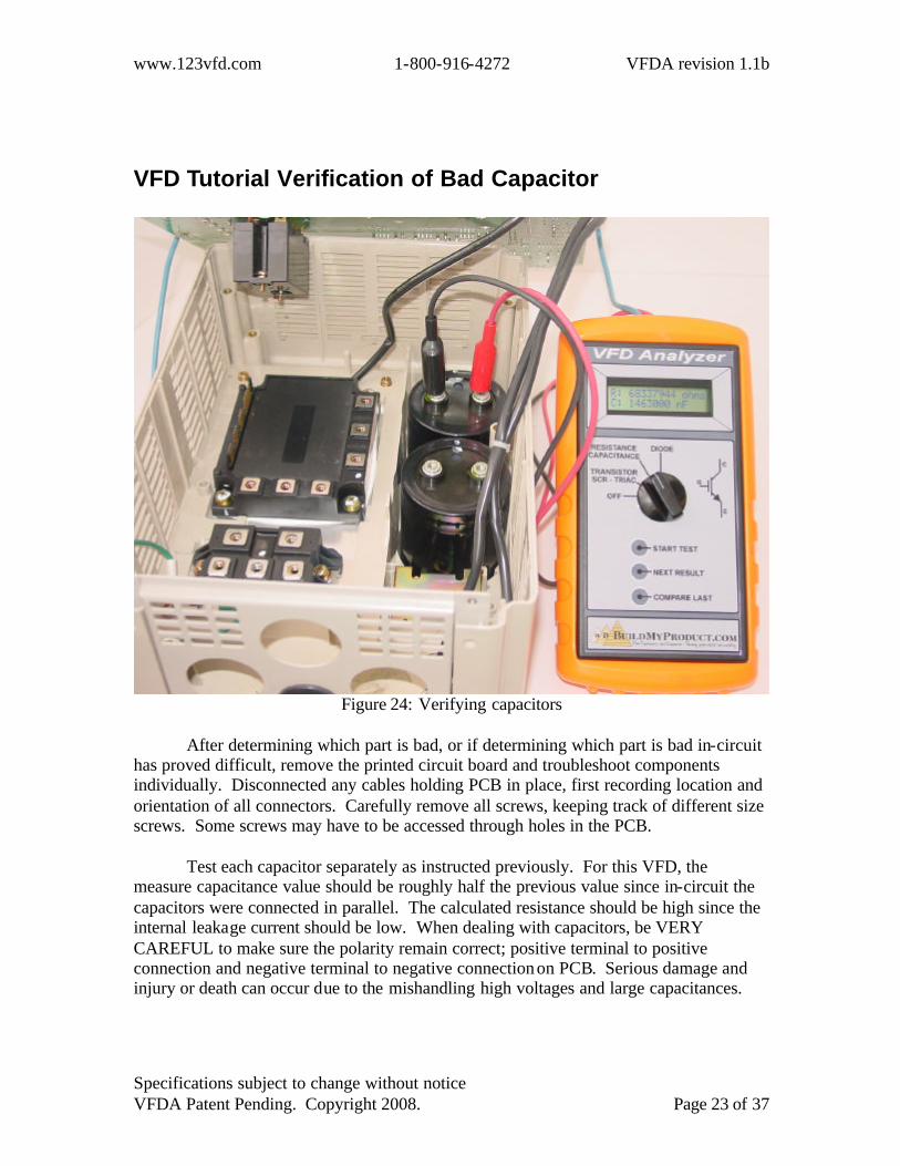
VFD Tutorial Verification of Bad Capacitor
Figure 24: Verifying capacitors
After determining which part is bad, or if determining which part is bad in-circuit has proved difficult, remove the printed circuit board and troubleshoot components individually. Disconnected any cables holding PCB in place, first recording location and orientation of all connectors. Carefully remove all screws, keeping track of different size screws. Some screws may have to be accessed through holes in the PCB. Test each capacitor separately as instructed previously. For this VFD, the measure capacitance value should be roughly half the previous value since in-circuit the capacitors were connected in parallel. The calculated resistance should be high since the internal leakage current should be low. When dealing with capacitors, be VERY CAREFUL to make sure the polarity remain correct; positive terminal to positive connection and negative terminal to negative connection on PCB. Serious damage and injury or death can occur due to the mishandling high voltages and large capacitances.

www.123vfd.com 1-800-916-4272 VFDA revision 1.1b
Specifications subject to change without notice VFDA Patent Pending. Copyright 2008. Page 24 of 37
VFD Tutorial Verification of Bad Transistor Module
Figure 25: Verifying transistor module
After determining which part is bad, or if determining which part is bad in-circuit has proved difficult, remove the printed circuit board and troubleshoot components individually. Disconnected any cables holding PCB in place, first recording location and orientation of all connectors. Carefully remove all screws, keeping track of different size screws. Some screws may have to be accessed through holes in the PCB. Notice the transistor module (in Figure 25) has some markings that match Figure 1 (U, V, & W, and with P for “+” and N for “-”), but the other terminals are only numbered. In this case, it may be necessary to locate the schematic of this part if trial and error can not locate the transistors; some modules can not be tested by the VFDA due to complex internal circuitry (though these are not as common). The module part number is often on the side of the module, as seen in Figure 26. The data sheet of the module provides the internal schematic (Figure 27) which indicates which pin is connected to the gate of each of the six transistors.

www.123vfd.com 1-800-916-4272 VFDA revision 1.1b
Specifications subject to change without notice VFDA Patent Pending. Copyright 2008. Page 25 of 37
Figure 26: Transistor module
Figure 27: Transis tor module schematic found in data sheet

www.123vfd.com 1-800-916-4272 VFDA revision 1.1b
Specifications subject to change without notice VFDA Patent Pending. Copyright 2008. Page 26 of 37
Figure 28: Verifying first transistor in module.
Now, using the schematic of the part as seen in Figure 28, we can easily make the three probe connections and test the first transistor. Be sure to only connect the probe to the gate (blue probe two in Figure 28 above) and not to touch either of the pins on either side. If the results of the test are either “Probes Shorted” or “Probes Open”, and connection to the module terminals is good, then the component is most likely bad. If the transistor tests as good, continue testing the remaining transistors as done previously in this manual, using the module data sheet and Figure 1 as necessary. If the transistors are housed in separate modules and if one module is bad, the other modules may be significantly weakened due to the stress on the components when the first module failed. It may be in the best interest to replace all of the transistor modules connected to the output motor terminals (such as U, V, and W) at the same time. Note the probes must be connected to the tabs and not the nuts below them; the nuts merely allow the screws to hold the tabs very firmly to the PCB above. When replacing modules, be sure to use sufficient heat sink compound and torque to hold the module in place.

www.123vfd.com 1-800-916-4272 VFDA revision 1.1b
Specifications subject to change without notice VFDA Patent Pending. Copyright 2008. Page 27 of 37
VFD Tutorial Other Components
Figure 29: Testing
The VFDA can be used to troubleshoot other components in the VFD. The VFD used in this tutorial has brake, which is not common to all VFDs. If the brake transistor failed by shorting permanently, the motor might not want to turn at all; if the brake transistor failed by never closing, the drive would not be able to slow the motor. Using Figure 25 and 27, we can determine the probe connections to test this transistor, as is shown in Figure 29. Using the DIODE procedures of the manual, we can also test the diode between pins “B” and “P” of this module. The brake resistors located elsewhere on the PCB can also be tested with the RESISTANCE CAPACITANCE procedures of this manual. If any of these components fail in-circuit, remove them and verify they are not functioning, and then install a suitable replacement component.

www.123vfd.com 1-800-916-4272 VFDA revision 1.1b
Specifications subject to change without notice VFDA Patent Pending. Copyright 2008. Page 28 of 37
Transistor / Thyristor Test Probe Connection: The first step is to locate the pins of the transistor to be tested inside of the VFD. Too many types of VFDs are available on the market to illustrate them all, but the connections are similar because they reflect the basic circuit diagram shown in Figure 1. Though the modules may be on the underside of a printed circuit board (PCB), those transistor modules will look much like Figure A and Figure B below. If the component labeling can not be seen and/or the printed circuit board is not well marked, you can use Figure 1 and the following details to help locate a transistor’s pins.
Figure A. Two Semiconductors in One Housing for a single phase output.
The outputs of the VFD to the motor, often labeled “U”, “V”, and “W”, each connect to the Collector and Emitter of a pair of transistors. The connection to the PCB may be a solder terminal or screw terminal (as seen in figures above), but they will likely be large, perhaps about 1/4 inch or so in size. Clip one of the three VFDA probe leads onto one of these terminals. After locating the first pin of a transistor, the second pin of one of the transistors must be found, which will be very near by. In the case of Figure A, the motor output is the far left terminal shared by two components, thus both the middle and right screw terminals each are the second pin of either transistor. In Figure B, the output terminals are the bottom left three terminals; using Figure 1, it can be seen the terminal labeled “+”

www.123vfd.com 1-800-916-4272 VFDA revision 1.1b
Specifications subject to change without notice VFDA Patent Pending. Copyright 2008. Page 29 of 37
is tied to the Collectors of all three transistors whose Emitters are tied to motor outputs “U”, “V”, and “W”. Clip another probe lead onto the second pin of one of the transistors.
Figure B. Six Semiconductors in One Housing for a three phase output.
Lastly, the Gate or Base of the transistor must be located. The Gate of an IGBT or FET may be small as in Figure A, the bottom right solder terminal. The Base of an NPN transistor may be large, as in Figure B, which are the top right six screw terminals. Some trial and error may be necessary to locate all three pins, but once a transistor is found, a pattern can typically be determined for the remaining terminals. If the probes are not connected to a working transistor, the results “Probes Shorted” or “Probes Open” will be displayed. In such a case, the transistor as failed or the connections are wrong so either try another transistor first or move a probe to another terminal. The following table indicates the necessary terminal sets to test each transistor in the modules found in Figure A and Figure B. Remember, the order of which probe connected to which terminal is not required to test working transistors, but each pin of the transistor to be tested must be attached to a probe each of the VFDA. Figure 1 1 2 2 2 2 2 2 Transistor 1 2 1 2 3 4 5 6 Probe 1 C2E1 E2 U - V - W - Probe 2 G1 G2 B1 B2 B3 B4 B5 B6 Probe 3 C1 C2E1 + U + V + W
Table 1

www.123vfd.com 1-800-916-4272 VFDA revision 1.1b
Specifications subject to change without notice VFDA Patent Pending. Copyright 2008. Page 30 of 37
If you are not testing a module, but rather a single transistor or thyristor, hook up is very straight forward. Connect each terminal or pin of the transistor to separate probes of the VFDA. Running Test: After the probes have been connected to the transistor or thyristor, turn the rotary switch from OFF to TRANSISTOR SCR TRIAC setting. The entire test is performed without further operator intervention. Wait for the testing to be complete, as the screen will step through “T_stor Setup”, “Attempting Probe Configuration”, and “Test Passed” displays. The first stage configures the VFDA for the desired test, and the second stage tests all of the possible pin configurations. If a good transistor or thyris tor is found, the test is repeated multiple times, since some component failures occur intermittently at first. Displayed Results: When the test is finished, the display will scroll through the test results. First, the problem or component found is displayed. Second, the last successful tested configuration is report by indicating both the probe number and its corresponding pin: collector, emitter, or gate. Lastly, the VFDA will scroll through all of the measured voltages and currents with the measured while testing the component. These values are more useful qualitatively than quantitatively since they do not represent the actual voltages and current under which the VFD would operate. Pressing the NEXT RESULT button will advance the display to the next test result. The following details provide further details on the results displayed.
Text Displayed Meaning IGBT/NFET Good A working IGBT or NFET is connected to the probes. Since
they both have higher gate voltages and lower gate currents when operating, the VFDA can not tell them apart.
NPN BJT Good A working NPN BJT transistor is connected to the probes. PNP BJT Good A working PNP BJT transistor is connected to the probes.
P FET Good A working PFET transistor is connected to the probes. Thyristor Good A working SCR or Triac is connected to the probes. Probes Shorted One of the above components was not found, and high current
was detected traveling from one probe to another during test. See Troubleshooting for tips to deal with this result.
Probes Open One of the above components was not found, and low current was detected traveling from one probe to another during test. See Troubleshooting for tips to deal with this result.
Table 2: Results Found Displayed Configuration: After the initial results are displayed, the configuration is displayed in the following format: “Probe 1: x 2: y 3: z”. The x, y, and z will indicate one of each of the three values: Collector, Emitter, or Gate. Collector will be abbreviated as either Collect or Cltr. This information could be useful in several situations. Using this information and Figure 1 may help more quickly identify the terminals of other transistors in a module or help locate the terminals of other

www.123vfd.com 1-800-916-4272 VFDA revision 1.1b
Specifications subject to change without notice VFDA Patent Pending. Copyright 2008. Page 31 of 37
components in the VFD. When testing individual transistors or thyristors, this may negate the need to look up data sheets when trying to find a replacement component. Displayed “Off Vce” and “Off Ic”: The transistor or thyristor should not pass current through the Collector when the component is off even though the VFDA applies voltage across the Collector to the Emitter. Thus the measured voltage should be high (closer to 12 volts than 0 volts) and the measured current low (closer to 0mA than 100mA). After testing a second similar component (by pressing the START TEST button), the resulting data can be displayed in percentages of the previous test results instead of in volts and mA by pressing the COMPARE LAST button; this allows quick comparison through multiple parts. Displayed “Off Vge” and “Off Ig”: The transistor or thyristor is off when the VFDA attempts to pull the Gate down same voltage as the Emitter. Thus the measured voltage should be low (closer to 0 volts than 12 volts) and the measured current low (closer to 0mA than 100mA). If significant voltage or current is present, either the correct terminals in a transistor module have not been located or the component is defective. Displayed “On Vce” and “On Ic”: The transistor or thyristor should pass significant current through Collector and the voltage across the Collector the Emitter should drop when the component is on. Thus the measured voltage should be lower than it was when it was off, and the measured current significantly higher (above 50mA). Displayed “On Vge” and “On Ig”: The current and voltage of the transistor or thyristor being tested affects the values that should be displayed for a working component. An on IGBT or FET should both have significantly higher voltage than when it was off, but the on current should be only somewhat higher than the off current. For a Bi-polar Junction Transistor or a thyristor, the on current should be significantly higher than the off current, but the on voltage should be only somewhat higher than the off voltage. Displayed “Off Vak” and “Off Ia”: Unlike transistors, thyristors should continue conducting current even after the controlling gate is turned back off by the VFDA. Therefore, when a working thyristor is found, the measured voltage should be lower and the measure current should be higher than it was when it was first off. This category of display data will not appear if the VFDA does not detect a working thyristor. Further Notes on Transistor and Thyristor Testing : The VFDA is designed to test components in-circuit in many different types of VFDs; this prevents exact measurements but the VDFA results are adequate to see if the component is functioning. Thyristors requiring a holding current higher than a couple hundred mA may not be adequately tested by this device. PNP or P channel components have the opposite polarity, and the display will indicate such with a “-“ when such a component has been found.

www.123vfd.com 1-800-916-4272 VFDA revision 1.1b
Specifications subject to change without notice VFDA Patent Pending. Copyright 2008. Page 32 of 37
When testing an SCR, if the results indicate the component found is a PNP BJT, try changing the configuration of the probes. The last configuration the VFDA tries: Probe 1 as the Emitter (or Cathode), Probe 2 as the Gate, and Probe 3 as the Collector. A functioning SCR may appear to the VFDA as a PNP if the exact configuration does not match the configuration outlined above. Some IGBTs modules have a built in pre-driver circuit that will make analyzing with the VFDA difficult or impossible. This extra circuit may require power to be supplied on a fourth terminal before an IGBT will operate. The VFDA can not address every possible module configuration, but has been optimized for the most common.
Capacitance and Resistance Testing The VFDA can help determine if the capacitor bank or bleed resistor, as seen in the Fixed DC Voltage stage of Figure 1, is not functioning properly while the components are in-circuit, allowing diagnosis without having to disconnect them. The correct terminals must first be determined for testing, and then the VFDA will take and report all necessary measurements. Connecting Probes: The positive and negative bus rails, to which the capacitor is connected, must be located. If the TRANSISTOR SCR TRIAC test or DIODE test has already been completed successfully, the terminals have already been located. Using Figure 1, the VFD transistors that share common collectors and the VFD diodes that share common cathodes are tied to the positive bus rail. The VFD transistors that share common emitters and the VFD diodes that share common anodes are tied to the negative rail. Probe 1 must be connected to the negative rail or negative terminal of the capacitor, and Probe 3 must be connected to the positive rail or positive terminal of the capacitor. Probe 2 is not used for this test, and should be disconnected. Sometimes the PCB of the VFD will be marked with a “+” to indicator the terminal(s) for the positive side of the capacitor and “-“ for the negative side of the capacitors. If the VFD diodes or transistors, as shown in Figure 1, are properly working, connecting the capacitor to the VFDA backwards should not cause damage but only incorrect readings. If a polarized capacitor is connected to the VFDA backwards and that capacitor is NOT protected by a diode, damage may results. If a polarized capacitor, RATED BELOW 12 volts, is connected to the VFDA in either orientation, damage may results. Running Test: Turn the VFDA rotary switch from OFF to the RESISTANCE CAPCITANCE setting. For the typical VFD test, the display will update with “Draining Voltage”, “RC Test Setup”, “Measur ing C”, and “Measuring RC”. If the capacitor has residual voltage from a previous VFDA test, it will first drain that voltage. Next the VFDA will be prepared for the test. Then the capacitance of the probe connections will be measure while charging the capacitor; the charge voltage is displayed on screen while charging. After the capacitor is significantly charged, the VFDA will measure the time constant of the circuit while allowing the capacitor to drain through any connected

www.123vfd.com 1-800-916-4272 VFDA revision 1.1b
Specifications subject to change without notice VFDA Patent Pending. Copyright 2008. Page 33 of 37
resistance. Lastly the resistance of the circuit is calculated, and all of the measured values are displayed. Running Test on Low Capacitance : If the capacitance connected to the probes is too small for the VFDA to adequately measure, the resistance is first measured while “Measuring R” is displayed on the screen. Then the time constant of the circuit is measured, and the capacitance is calculated. Displayed Results: The results from the test are displayed consecutively. Pressing the NEXT RESULT button advances to the next data result. First the measured RC time constant value is displayed along with the result summary. Second the VFDA displays the resistance and capacitance, one value of which was measured and the other calculated. Then the VFDA displays the assumed connections to the circuit under test, with Probe 1 connected to negative terminal of the capacitor and Probe 3 connected to the positive terminal of the capacitor. The VFDA first displays either “VFD RC Low” or “VFD RC Good” followed by the measured RC time constant. “VFD RC Low” means the connected resistance and capacitance network discharged very quickly, and is likely insufficient to hold power properly for a VFD. “VFD RC Good” indicates the time constant is greater than 10 seconds, meaning it takes more than 10 seconds for the voltage of the connected circuit to drop by approximately 63% of its initial value. If the displayed RC value is really high, over a couple hundred of seconds, the bleed resistor of the VFD may not be functioning properly causing a safety hazard for technicians. Next, the VFDA displays both the resistance and capacitance determined during the test. The VFDA automatically determines which value it can most accurately measure, then measures the RC time constant, and calculates the other result. Some single component measurements produce inaccurate calculated results. For example, connecting only a single resistor to the VFDA probes will produce a useless capacitance calculated value since the RC time constant measured reflects the floating probes capacitance.

www.123vfd.com 1-800-916-4272 VFDA revision 1.1b
Specifications subject to change without notice VFDA Patent Pending. Copyright 2008. Page 34 of 37
Diode Testing The VFDA reports the status of the of the Rectifier Circuit stage (Figure 1) of the VFD using the Diode test. The VFDA allows higher current testing of diodes than standard multimeters which may locate problems others might miss. When testing diodes with any meter, some technical considerations must be kept in mind. After testing, the VFDA will first display whether it found None, One, or Two diodes. Then the VFDA will display the found diode configuration followed by the each diodes measured voltage and current. The VFDA may also verify some diodes in-circuit where standard meters may not due to the ability to source higher current; common for low resistance or high capacitance parallel components.
Figure C
Diode Testing Problems : Testing diodes, regardless of testing device, requires simply understanding of diodes. First diode testing with a standard multimeter is addressed, followed by testing with the VFDA. The advantages of using the VFDA will then be apparent. This discussion will use Figure C above, and notation to simplify the discussion is as follows. Placing the positive lead probe of a standard multimeter on test point A (cathode of diode 1) is indicated by “A+ve”, and the negative lead of a standard mulitmeter on test point B (anode of diode 1) is indicated by “B-ve”. Placing probe 1 of the VFDA on test point B is notated by “B1”, probe 2 on test point C as “C2”, and probe 3 on test point D as “D3”. A standard mulitmeter requires the movement of the probes to test each diode since a diode will allow current flow in one direction but not the other. Placing the meter on A+ve and B-ve of diode one displays an overload condition, often “OL”, to indicate the measured voltage is above a typical diode. The meter probes must then be changed to A-ve and B+ve, and then the meter will only display the voltage measured across the diode at some unknown small current. Using the VFDA by placing the probes in orientation of A1 and B2 or orientation of A2 and B1 will display the diodes configuration, tested voltage, and tested current on the VFDA screen.

www.123vfd.com 1-800-916-4272 VFDA revision 1.1b
Specifications subject to change without notice VFDA Patent Pending. Copyright 2008. Page 35 of 37
Unexpected results can result from probe placement. Placing a standard multimeter on B+ve and D-ve will display the total voltage drop of diode two plus diode three. The VFDA will also only find one diode with connections of B1, D2, and probe 3 left disconnected. Because typical voltage diode drops are less than one volt and can vary, the VFDA has no way to identify how many diodes are between any two given probes. Simply using a third probe does not guarantee success since in-circuit other components could also affect results, but three probe VFDA diode tests are discussed shortly. Common Cathode or common Anode diode connections also pose problems. Placing a standard multimeter at A+ve and C-ve produces the “OL” condition, and likewise the A-ve and C+ve. The VFDA has been optimized to locate diodes for the typical VFD configuration (seen in Figure 1) is much like the connection between diode two and diode three therefore testing of common Cathode (diodes three and four) or common Anode (diodes one and two) diode configurations must be tested individually using probes 1 and 2 with probe 3 disconnected. Diode Testing with VFDA: For testing diode pairs (connected like diodes two and three in Figure C) simply connect all three probes. The test points for the diode commons on a VFD are typically the input power connections, often L1, L2, and L3 ; the positive rail is typically connected to an anode of each pair while the negative bus rail is typically connected to the cathodes. After successfully testing first pair of diodes in a VFD, simply move the Probe connected to both an anode and a cathode to the next pair of diodes (if there are multiple phases). When testing diodes individually, use only two probes while leaving the remaining probe disconnected. Running Test: Turn the VFDA rotary switch from OFF to the DIODE setting. For the typical VFD test, the display will update with “Diode Test Setup” and “Configuration”. First the VFDA will be prepared for the test. Then the VFDA will step through all of the possible diode configurations testing for diodes between the probes. Displayed Results: The VFDA will scroll through the results found. First, the number of diodes found is reported: None, One, or Two. Next the diode configuration found is displayed, which is further explained below. Lastly, the measured current and voltage through the diode are displayed. Pressing the NEXT RESULT button advances to the next data result. After testing a second similar diode or diode pair (by pressing the START TEST button), the resulting data can be displayed in percentages of the previous test results instead of in volts and mA by pressing the COMPARE LAST button; this allows quick comparison of multiple parts. The diode configuration is displayed like diodes two and three in Figure C above. The probe numbers are inserted at locations B, C, and D to indicate the configuration measured. An example might be “ 3 ->|- 2 ->|- 1”, indicating the first diode found is between probes 3 and 2 with the anode connected to probe 3; the second diode found between probes 2 and 1 has the cathode of the second diode connected to probe 1.

www.123vfd.com 1-800-916-4272 VFDA revision 1.1b
Specifications subject to change without notice VFDA Patent Pending. Copyright 2008. Page 36 of 37
The measured data for first diode is displayed, followed by the data for the second diode. It is import to observe the location of the diode in the configuration displayed when only one diode was found. If the results were “3 ->|- 2 1”, then the first diode results (Vd1 and Id1) contain the measured values. If the results were “3 2 ->|- 1”, then the second diode results (Vd2 and Id2) contain the measured values. Further Notes on Diode Testing : When testing diodes with higher voltage drops (>3 volts) with high currents, such as light emitting diodes, a specific configuration is necessary. For diode pair testing, always use probe 3 for the anode, probe 2 for the common, and probe 1 for the cathode; for single diode testing, use only probes 3 and 2 or probes 2 and 1 as described previously while leaving the remaining probe disconnected. The VFDA “finds” a diode by seeing a voltage drop of less than three volts, and the last diode configuration tested is described as above. The VFDA will still report “No Diode Found”, but the VFDA will then display the measured voltage and current of the indicated configuration.

www.123vfd.com 1-800-916-4272 VFDA revision 1.1b
Specifications subject to change without notice VFDA Patent Pending. Copyright 2008. Page 37 of 37
Troubleshooting Test Setup Long : If the VFDA spends 15 seconds or more at the Test Setup stage, the batteries are probably running low. Swapping the batteries may help for a short period of time, since one battery has a larger load than the other. The best course of action is to replace with fresh primary 9V batteries or fully charged rechargeable 9V batteries. Not all rechargeable batteries are guaranteed to operate the VFDA properly; batteries with a charge over 10 volts are not recommended. Probes Shorted: This indication from the VFDA typically means the measured current from one probe to another is high while the voltage measured across those two probes is low. This can results from connecting two probes to two terminals that have very low resistance. Often a VFD will have multiple components connected by a single trace or bus bar. The first course of action is to confirm no VFDA probe is connected to another probe via a metal trace or bus bar; the RESISTANCE test may be useful for this purpose. A second reason for condition is the probes are shorted together through a bad component, in which case the VFDA has identified a bad component needing replacement. After re-checking connections, re-running the VFDA test, and confirming connections with any available schematics or similar circuits, removal of the suspected component and re-checking it with the VFDA once more is the recommended procedure. Probes Open: This indication from the VFDA typically means the measured current from any probe to the others is low while the measured voltage across any two probes is high. This can result when probes do not have a good connection to a component, connected to unrelated components, or connected correctly to a component that is not functioning properly. The first course of action is to reconnect the probes to the terminals, trying to press through any surface debris. Scraping the terminals may be necessary if excess debris or coating prevents a good connection. After re-checking connections, re-running the VFDA test, and confirming connections with any available schematics or similar circuits, removal of the suspected component and re-checking it with the VFDA once more is the recommended procedure.


