Variation-aware Clock Network Design Methodology forUltra-Low Voltage (ULV) Circuits
Xin Zhao, Jeremy R. Tolbert, Chang Liu, Saibal Mukhopadhyay, and Sung Kyu LimSchool of ECE, Georgia Institute of Technology, 777 Atlantic Dr. NW, Atlanta, GA 30332, U.S.A.
Abstract—This paper presents a design methodology for robust andlow-energy clock networks for ultra-low voltage (ULV) circuits. We showthat both clock slew and skew play important roles in achieving highmaximum operating frequency (Fmax) and low clock energy in ULVcircuits. In addition, clock networks in ULV circuits are highly sensitiveto process variations. We propose a variation-aware methodology thatcontrols both clock skew and slew to maximize Fmax and minimize clockpower. Experimental results show that our clock network design methodachieves lower energy (more than 20 % savings) at comparable or evenhigher Fmax compared with the existing methods.
Ultra-low voltage (ULV) circuits, where the supply voltage isaround or even below the threshold voltage of transistors, haveemerged as an attractive option for ultra-low-power digital computing.Many ultra-low-power battery-operated applications with a stringentenergy budget can benefit from operating in ULV, such as biologicalmonitoring systems, radio frequency identification devices, wirelesssensor networks, etc. Though speed is not the primary goal, highfrequency operation has been demonstrated in the range of tens tohundreds of megahertz [1] with ULV circuits.
In the ULV domain, clock slew plays a major role in robustnessof the clock network. This is because in ULV, buffer delay and flip-flop timings (set-up, clock-to-q, and hold) are strong functions ofclock slew [2], [3]. In addition, ULV circuits are more sensitive toprocess and environmental variations, especially threshold voltagerandom variability [4]. In the ULV domain, the device currentdepends exponentially on threshold voltage. Hence, threshold voltagevariability can cause a significant variation in clock skew and slew,thereby degrading the timing margins. As a result, the operatingfrequency is usually reduced to ensure correct operation. Therefore,the clock design methodology for ULV circuits requires (1) efficientcontrol on both clock slew and skew, (2) robustness in the presence ofvariations, (3) consideration of frequency target, and (4) low energyclock operation.
The history on ULV clock network design is very brief. Existingworks focus on minimizing either clock slew or clock skew butnot both. Tolbert et al. [2] pointed out the importance of clockslew control for the reliability of subthreshold circuits and presentedclock trees that control clock slew while minimizing the energy.However, they did not consider the impact on clock skew. Seoket al. [5] compared buffered and unbuffered H-trees and claimedthat an unbuffered H-tree helps skew minimization. However, theyneglected the effect of slew, which significantly worsens in anunbuffered H-tree. To counter the slew effect, a larger driver is usedin their tree, resulting in a significant energy penalty. In addition,both of these works are primarily circuit-level studies and did notpresent any design method for clock network synthesis. As large-scale ULV circuits are emerging, methodology is becoming essential
This material is based upon work supported by the NSF under Grant No.CCF-0917000 and NSF Graduate Fellowship No. DGE-0644493.
for automated synthesis of robust (low-slew and low-skew) and low-energy clock network.
In this paper, we develop a variation-aware methodology for robustand low-energy clock network design for ultra-low voltage circuits.The contributions of this paper are as follows.
• We present a comprehensive study based on extensive experi-mental results that show the impact of clock skew and clockslew control on power consumption, performance, and variationtolerance in ultra-low voltage (ULV) circuits.
• We develop a variation-aware ULV clock network designmethodology. For clock skew management, we construct therouting topology and insert buffers to minimize the delay differ-ences among the clock paths under both nominal and statisticalconditions. We also show how to efficiently control clock slewbound at each sink under both nominal and statistical conditions.Our algorithm generates and saves multiple solutions to achieveminimum clock energy.
• Experimental results show that our clock design method is ableto efficiently control the clock skew and slew in both nominaland statistical conditions, and construct ULV clock networkswith low clock energy at a high maximum operating frequency.We outperform state-of-the-art ULV clock routing methods [2],[5] in terms of performance and energy under both nominal andstatistical conditions.
II. MOTIVATION
A. Clock Slew and Skew Impact on Timing of ULV Circuits
Our work is motivated by the impact of both clock skew and slewon the cycle time. The schematic in Figure 1 shows a generic logicpath composed of fan-out-4 NAND gates between two registers. It in-cludes the clock-to-q (TCLK-Q), the setup time (Tsetup), the combinationlogic path delay (Tlogic), and the difference of the clock arrival times(Skew). The minimum cycle time (Tmin) and the maximum clockfrequency (Fmax = 1/Tmin) for the above system is given below:
where TmaxLogic is the maximum logic path delay. This circuit operates at
550 mV supply voltage, where nominal threshold voltage for NMOSand PMOS is 621 mV and -575 mV, respectively. First, a larger skewincreases Tmin, thus decreases Fmax. Second, clock slew directly altersthe timing metrics TCLK-Q and Tsetup, leading to a long cycle time.Clock slew could vary the hold time as well [3], [6].
Figure 2 shows the path length (= N ) vs. Fmax trend for four casesin ultra-low voltage (ULV) circuits: (1) Optimal: 1.5 ns clock slewand 0 ns clock skew; (2) Skew-only: clock skew (CLK1 arrives laterthan CLK2) is 5 % of the optimal period, and the clock slew is 1.5 ns;(3) Slew-only: 10 ns clock slew and 0 ns skew; (4) Slew+skew: slewaround 10 ns, and skew is 5 % of the optimal period. We observe thatdue to the additional amount of skew (or slew), Case 2 (or Case 3)obtains lower operating frequency than Case 1 at each logic length.
Fig. 1. A data path in synchronous ultra-low voltage (ULV) circuit.
Fig. 2. Impact of the logic path length on Fmax of ultra-low voltage (ULV)circuit in 550 mV Vdd under four combinations of clock skew and slew.
In Case 4, where both skew and slew degradation are applied, Fmax
is degraded from 12 % to 20 %, depending on the length of the logicpath. This clearly shows that both clock skew and slew affect theoperating frequency significantly in ULV circuits.
Figure 3 shows the detailed timing metrics with respect to the slewin ULV circuits, where the path length is fixed to 10. We observe thatboth TCLK-Q and Tsetup increase by 51 % and 61 % if the slew increasesfrom 1.5 ns to 10.5 ns. Note that data slew is recovered within the FFs.The logic delay remains unaffected by the clock slew change. As ULVsystems target higher frequencies (i.e., as the logic path reduces),the timing metrics (TCLK-Q and Tsetup) become a large portion of thecycle time and thus can not be ignored. This clearly demonstratesthe importance of clock slew on ULV circuit performance.
B. Impact of Buffer Placement on ULV Clock Wires
In ULV circuits, the effect of interconnect resistance is negligi-ble [2], [5] due to the large resistance of the driving buffer. Thisalso allows the interconnect to be modeled as a lumped capacitance.Seok et al. [2] pointed out that adding more buffers in the middle of acapacitive interconnect does not help reduce the delay. However, weobserve that a buffered interconnect is advantageous to improve slewunder comparable power consumption. This means that to achievethe same slew, using many but smaller buffers consumes lower powerthan simply using one large buffer to drive the entire clock network.
Figure 4 demonstrates how the buffer count and location affectthe sink slew and src-to-sink delay in ULV circuits. We comparetwo cases: (1) using a large driver (= B0) for a long interconnect(1000 μm); (2) using two small buffers (= B1 and B2) to drive theinterconnect. The sink slew and src-to-sink delay in the two-buffercase are normalized to the one-buffer case results. While keepingB1 at the source location, we note that moving B2 towards the sink
Fig. 3. Impact of clock slew on Tlogic, TCLK-Q, and Tsetup in ULV circuit(Vdd = 550 mV). The path length is set to 10.
B2B1 B2 B2 B2
d14X Buf 4X Buf
B0src
8X Buf
sink(a)
(b)
Fig. 4. Impact of the buffer count and buffer location on the sink slew andthe src-to-sink delay in ultra-low voltage (ULV) circuits.
causes the sink slew to decrease up to 80 % and outperform the one-buffer case. on the other hand, the overall delay increases. Note thatboth cases consume similar power. This shows that a buffered clocktree has the potential to improve slew and achieve lower power, butcare must be taken to control clock skew in ULV circuits.
III. ULV CLOCK NETWORK DESIGN METHODOLOGY
The ultra-low voltage clock tree synthesis (ULV-CTS) problem isformulated as follows: Given a set of clock sinks, a target sink slew,and an upper bound for clock skew, the ULV-CTS is to construct abuffered clock tree such that: (1) clock slew at sink node is underthe given constraint; (2) clock skew is under the given constraint;(3) clock power is minimized; (4) the clock skew and clock slewvariability are controlled. Given various slew and skew upper boundconstraints, we can generate clock networks with different Fmax.
We develop a ULV clock buffering and routing method that consistsof two steps: (1) abstract tree generation that determines the hier-archical connection among the sink nodes, intermediate nodes, andthe root node; (2) clock routing and buffer insertion that decide the
10
Par��on line
14
3
5
7
6
21
4
3
5
7
6
2
root
driver
buf
1 2 6 7 4 35
root
a b c
d e
u v
p
7 X
1 2 6 7 4 3
5
root
a b c
d e
Abstract tree Abstract tree a�er DP+DME
Buffering and merging, bo�om-up and top-down
Samples of buffering topology
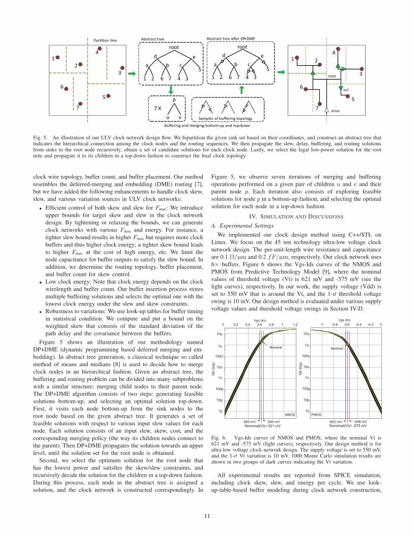
Fig. 5. An illustration of our ULV clock network design flow. We bipartition the given sink set based on their coordinates, and construct an abstract tree thatindicates the hierarchical connection among the clock nodes and the routing sequences. We then propagate the slew, delay, buffering, and routing solutionsfrom sinks to the root node recursively, obtain a set of candidate solutions for each clock node. Lastly, we select the legal low-power solution for the rootnote and propagate it to its children in a top-down fashion to construct the final clock topology.
clock wire topology, buffer count, and buffer placement. Our methodresembles the deferred-merging and embedding (DME) routing [7],but we have added the following enhancements to handle clock skew,slew, and various variation sources in ULV clock networks:
• Efficient control of both skew and slew for Fmax: We introduceupper bounds for target skew and slew in the clock networkdesign. By tightening or relaxing the bounds, we can generateclock networks with various Fmax and energy. For instance, atighter slew bound results in higher Fmax but requires more clockbuffers and thus higher clock energy; a tighter skew bound leadsto higher Fmax at the cost of high energy, etc. We limit thenode capacitance for buffer outputs to satisfy the slew bound. Inaddition, we determine the routing topology, buffer placement,and buffer count for skew control.
• Low clock energy: Note that clock energy depends on the clockwirelength and buffer count. Our buffer insertion process storesmultiple buffering solutions and selects the optimal one with thelowest clock energy under the slew and skew constraints.
• Robustness to variations: We use look-up tables for buffer timingin statistical condition. We compute and put a bound on theweighted skew that consists of the standard deviation of thepath delay and the covariance between the buffers.
Figure 5 shows an illustration of our methodology namedDP+DME (dynamic programming based deferred merging and em-bedding). In abstract tree generation, a classical technique so calledmethod of means and medians [8] is used to decide how to mergeclock nodes in an hierarchical fashion. Given an abstract tree, thebuffering and routing problem can be divided into many subproblemswith a similar structure: merging child nodes to their parent node.The DP+DME algorithm consists of two steps: generating feasiblesolutions bottom-up, and selecting an optimal solution top-down.First, it visits each node bottom-up from the sink nodes to theroot node based on the given abstract tree. It generates a set offeasible solutions with respect to various input slew values for eachnode. Each solution consists of an input slew, skew, cost, and thecorresponding merging policy (the way its children nodes connect tothe parent). Then DP+DME propagates the solution towards an upperlevel, until the solution set for the root node is obtained.
Second, we select the optimum solution for the root node thathas the lowest power and satisfies the skew/slew constraints, andrecursively decide the solution for the children in a top-down fashion.During this process, each node in the abstract tree is assigned asolution, and the clock network is constructed correspondingly. In
Figure 5, we observe seven iterations of merging and bufferingoperations performed on a given pair of children u and v and theirparent node p. Each iteration also consists of exploring feasiblesolutions for node p in a bottom-up fashion, and selecting the optimalsolution for each node in a top-down fashion.
IV. SIMULATION AND DISCUSSIONS
A. Experimental Settings
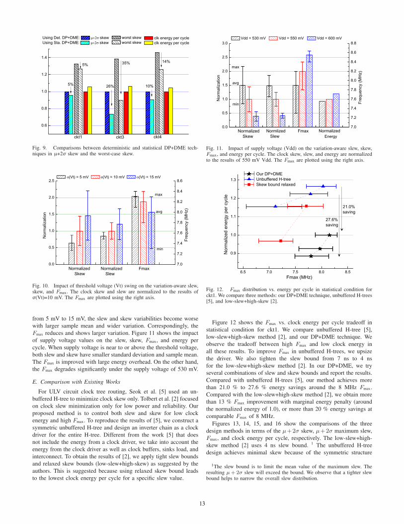
We implemented our clock design method using C++/STL onLinux. We focus on the 45 nm technology ultra-low voltage clocknetwork design. The per-unit-length wire resistance and capacitanceare 0.1 Ω/μm and 0.2 fF/μm, respectively. Our clock network uses6× buffers. Figure 6 shows the Vgs-Ids curves of the NMOS andPMOS from Predictive Technology Model [9], where the nominalvalues of threshold voltage (Vt) is 621 mV and -575 mV (see thelight curves), respectively. In our work, the supply voltage (Vdd) isset to 550 mV that is around the Vt, and the 1-σ threshold voltageswing is 10 mV. Our design method is evaluated under various supplyvoltage values and threshold voltage swings in Section IV-D.
Ids
(log)
1p
10p
100p
1n
10n
100n
1u
10u
Vgs (lin)0 0.2 0.4 0.6 0.8 1 1.2
Vgs (lin)-1 -0.8 -0.6 -0.4 -0.2 0
Ids
(log)
1p
10p
100p
1n
10n
100n
1u
10u
Nomimal(Vt)= 621 mV650 mV593 mV
Nomimal(Vt)= -575 mV-603 mV -548 mV
NominalNominal
NMOS PMOS
Fig. 6. Vgs-Ids curves of NMOS and PMOS, where the nominal Vt is621 mV and -575 mV (light curves), respectively. Our design method is forultra-low voltage clock network design. The supply voltage is set to 550 mV,and the 1-σ Vt variation is 10 mV. 1000 Monte Carlo simulation results areshown in two groups of dark curves indicating the Vt variation.
All experimental results are reported from SPICE simulation,including clock skew, slew, and energy per cycle. We use look-up-table-based buffer modeling during clock network construction,
11
TABLE IINFORMATION OF BENCHMARK AND ENERGY PER CYCLE (PJ).
Energy per cycleckt Function #Gates #FFs Area logic+wire H-tree
Fig. 7. A sample layout of a clock network for a FIR filter with 619 clocksinks and 24937 μm wirelength.
and evaluate the designs using SPICE: (1) we extract the layoutinformation of the flip-flops (FFs); (2) apply our ULV clock synthesismethod to construct a buffered clock tree; (3) extract a clock netlistfor SPICE simulation. In statistical condition, the Vt uncertainty ismodeled as random variables with spatial uncorrelated [10]. We apply1000 Monte Carlo simulations for each design and report μ+2σ skewand slew like the existing work [5]. We created five benchmarkcircuits: three finite impulse response (FIR) filters, a multiplier, anda design implementing quick sort as shown in Table I.
Figure 7 shows a clock network for our FIR filter, which is seen infront of the logic cells and highlighted flip-flops. The clock networkhas 619 clock sinks, a total wirelength of 24937 μm, and die area of857 μm×924 μm.
B. Impact of Slew and Skew Bounds on Fmax and Energy
Figure 8 shows the impact of skew and slew upper bounds onFmax and clock energy per cycle for ckt1. We show four curves ofnominal results: one is for unbuffered H-trees, and the other three aregenerated by our DP+DME clock synthesis technique. The unbufferedH-tree takes an advantage of skew minimization. However, it needsa large driver for entire network to ensure small clock slew at sinknodes. Therefore, we upsize the driver (an inverter chain) to improvethe Fmax. As a result, the overall clock energy of unbuffered H-treeincreases significantly. In the case of DP+DME, we present threegroups of results, where clock networks in each group are designedunder the same skew bounds (1 ns, 3 ns, and 10 ns) but differentslew bounds (from 3 ns to 8 ns).
First, Figure 8 demonstrates the tradeoff between high Fmax andlow clock energy, i.e., design for a higher Fmax consumes more clock
Fig. 8. Fmax vs. energy per cycle in nominal condition for ckt1.
energy. In each DP+DME curve under the same skew constraint,a tighter slew bound improves Fmax. Meanwhile, the clock energyper cycle increases due to more buffers are inserted for tighter slewcontrol. Second, the design of 3 ns skew bound consumes lowerenergy than 1 ns skew bound. This is mainly because the 3 nsskew constraint reserves more feasible solutions during clock networkconstruction, which helps to obtain a low energy clock network.However, using relaxed skew bound of 10 ns cannot hold this benefit,since it allows larger clock skew thus requires more buffers fortighter slew to reach a similar Fmax as 1 ns or 3 ns skew bound.Third, compared with the unbuffered H-tree design targeting at skewminimization only, our method achieves up to 30 % energy reductionin the frequency range from 8.0 MHz to 8.4 MHz. This is because abuffered clock tree has shorter wirelength and a smaller driver thanthe unbuffered H-tree design. We note that a higher Fmax target willshorten the energy gap between ours and the unbuffered H-tree. Underthe relaxed skew bound, the clock energy increases slower than thatof tight skew bound as the slew bound increases. But, the relaxedskew bound results in lower Fmax than other two curves. Thus, wesee that by controlling both the skew and slew bounds, we design alow-energy clock network for a given target Fmax more effectively.
C. Statistical versus Deterministic Methods
Figure 9 shows the efficiency of our variation-aware methodology.We compare the deterministic and statistical DP+DME techniques interms of the μ+2σ skew, the worst-case skew, and the clock energy.There are two major differences between these two methods: (1)statistical DP+DME uses variation-aware LUTs, which includes thesample mean and standard deviation of delay and slew with respectto the input slew and loading capacitance, as well as the covariancebetween buffer delays; (2) we employ the statistical skew boundto cope with the control on the variation-caused skew uncertainty.We observe that both μ+2σ and the worst-case skew are efficientlyreduced by using the statistical method with marginal energy penalty.
D. Tolerance to Vdd and Vt Variations
Clock networks for ULV circuits are extremely sensitive to Vddand Vt variations. Thus, it is challenging and important to design arobust clock network aiming at both high Fmax and low energy underultra-low supply voltage and large threshold voltage fluctuations. Weshow the tolerance of our clock network to these variations. Figure 10shows the impact of threshold voltage swing on slew, skew, and Fmax
variability for ckt1. With the 1-σ threshold voltage swing increasing
12
Fig. 9. Comparisons between deterministic and statistical DP+DME tech-niques in μ+2σ skew and the worst-case skew.
Fig. 10. Impact of threshold voltage (Vt) swing on the variation-aware slew,skew, and Fmax. The clock skew and slew are normalized to the results ofσ(Vt)=10 mV. The Fmax are plotted using the right axis.
from 5 mV to 15 mV, the slew and skew variabilities become worsewith larger sample mean and wider variation. Correspondingly, theFmax reduces and shows larger variation. Figure 11 shows the impactof supply voltage values on the slew, skew, Fmax, and energy percycle. When supply voltage is near to or above the threshold voltage,both slew and skew have smaller standard deviation and sample mean.The Fmax is improved with large energy overhead. On the other hand,the Fmax degrades significantly under the supply voltage of 530 mV.
E. Comparison with Existing Works
For ULV circuit clock tree routing, Seok et al. [5] used an un-buffered H-tree to minimize clock skew only. Tolbert et al. [2] focusedon clock slew minimization only for low power and reliability. Ourproposed method is to control both slew and skew for low clockenergy and high Fmax. To reproduce the results of [5], we construct asymmetric unbuffered H-tree and design an inverter chain as a clockdriver for the entire H-tree. Different from the work [5] that doesnot include the energy from a clock driver, we take into account theenergy from the clock driver as well as clock buffers, sinks load, andinterconnect. To obtain the results of [2], we apply tight slew boundsand relaxed skew bounds (low-slew+high-skew) as suggested by theauthors. This is suggested because using relaxed skew bound leadsto the lowest clock energy per cycle for a specific slew value.
Energy
Fig. 11. Impact of supply voltage (Vdd) on the variation-aware slew, skew,Fmax, and energy per cycle. The clock skew, slew, and energy are normalizedto the results of 550 mV Vdd. The Fmax are plotted using the right axis.
Fig. 12. Fmax distribution vs. energy per cycle in statistical condition forckt1. We compare three methods: our DP+DME technique, unbuffered H-trees[5], and low-slew+high-skew [2].
Figure 12 shows the Fmax vs. clock energy per cycle tradeoff instatistical condition for ckt1. We compare unbuffered H-tree [5],low-slew+high-skew method [2], and our DP+DME technique. Weobserve the tradeoff between high Fmax and low clock energy inall these results. To improve Fmax in unbuffered H-trees, we upsizethe driver. We also tighten the slew bound from 7 ns to 4 nsfor the low-slew+high-skew method [2]. In our DP+DME, we tryseveral combinations of slew and skew bounds and report the results.Compared with unbuffered H-trees [5], our method achieves morethan 21.0 % to 27.6 % energy savings around the 8 MHz Fmax.Compared with the low-slew+high-skew method [2], we obtain morethan 13 % Fmax improvement with marginal energy penalty (aroundthe normalized energy of 1.0), or more than 20 % energy savings atcomparable Fmax of 8 MHz.
Figures 13, 14, 15, and 16 show the comparisons of the threedesign methods in terms of the μ+2σ skew, μ+2σ maximum slew,Fmax, and clock energy per cycle, respectively. The low-slew+high-skew method [2] uses 4 ns slew bound. 1 The unbuffered H-treedesign achieves minimal skew because of the symmetric structure
1The slew bound is to limit the mean value of the maximum slew. Theresulting μ+ 2σ slew will exceed the bound. We observe that a tighter slewbound helps to narrow the overall slew distribution.
Fig. 14. Comparison of unbuffered H-tree [5], low-slew+high-skew [2], andour DP+DME methods in μ+ 2σ maximum slew for ckt1 to ckt5.
and negligible interconnect resistance (see Figure 13). The low-slew+high-skew method [2] shows an advantage in minimizing thevariation-aware slew (see Figure 14). Because we efficiently controlboth clock skew and slew, our method guarantees a high Fmax (seeFigure 15) and outperforms the other two methods in terms of energy(i.e., 10 % to 30 % energy savings see Figure 16). In addition,the low-slew+high-skew method [2] achieves lower energy thanunbuffered H-tree at the cost of low Fmax. Therefore, we concludethat a simultaneous management of variation-aware slew and skewproves to be an efficient way to obtain a low-energy and robust clocknetwork targeting at a high Fmax in ULV circuits.
V. CONCLUSIONS
In this paper, we studied the methodology of low-energy androbust clock network design for ultra-low voltage (ULV) circuits.We observed that both clock slew and skew need to be accuratelycontrolled to ensure a high maximum operating frequency (Fmax) inULV circuits. We showed that buffer insertion is an important meansto achieve this goal. We proposed a variation-aware methodology thatcontrols both clock skew and slew to maximize Fmax and minimizeclock power. Experimental results show that we are able to constructclock trees that are variation-aware, low power, and high performance(= Fmax) while satisfying the given slew and skew constraints forultra-low voltage operations.
Fig. 16. Comparison of unbuffered H-tree [5], low-slew+high-skew [2], andour DP+DME methods in normalized energy per cycle for ckt1 to ckt5.
REFERENCES
[1] B. Paul, A. Raychowdhury, and K. Roy, “Device Optimization for DigitalSubthreshold Logic Operation,” IEEE Transactions on Electron Devices,vol. 52, no. 2, pp. 237–247, 2005.
[2] J. R. Tolbert, X. Zhao, S. K. Lim, and S. Mukhopadhyay, “Slew-awareClock Tree Design for Reliable Subthreshold Circuits,” in Proc. Int.Symp. on Low Power Electronics and Design, 2009, pp. 15–20.
[3] N. Verma, J. Kwong, and A. Chandrakasan, “Nanometer MOSFET Vari-ation in Minimum Energy Subthreshold Circuits,” IEEE Transactions onElectron Devices, vol. 55, no. 1, pp. 163–174, 2008.
[4] B. Zhai, S. Hanson, D. Blaauw, and D. Slyvester, “Analysis andMitigation of Variability in Subthreshold Design,” in Proc. Int. Symp.on Low Power Electronics and Design, 2005, pp. 20–25.
[5] M. Seok, D. Blaauw, and D. Sylvester, “Clock Network Design for Ultra-Low Power Applications,” in Proc. Int. Symp. on Low Power Electronicsand Design, 2010, pp. 271 –276.
[6] J. R. Tolbert and S. Mukhopadhyay, “Accurate Buffer Modeling withSlew Propagation in Subthreshold Circuits,” in Proc. Int. Symp. onQuality Electronic Design, 2009, pp. 91–96.
[7] K. Boese and A. Kahng, “Zero-skew clock routing trees with minimumwirelength,” in ASIC Conference and Exhibit, 1992., Proceedings of FifthAnnual IEEE International, 1992, pp. 17–21.
[8] M. Jackson, A. Srinivasan, and E. Kuh, “Clock Routing for High-Performance ICs,” in Proc. ACM Design Automation Conf., 1990, pp.573–579.
[9] Predictive Technology Model (PTM), http://ptm.asu.edu/.[10] N. Drego, A. Chandrakasan, and D. Boning, “Lack of Spatial Correlation
in MOSFET Threshold Voltage Variation and Implications for VoltageScaling,” IEEE Transactions on Semiconductor Manufacturing, vol. 22,no. 2, pp. 245–255, May 2009.