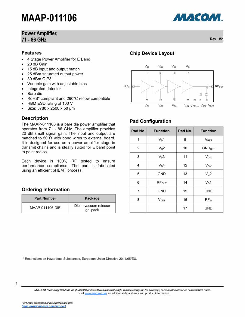
Power Amplifier, 71 - 86 GHz Rev. V2 MAAP-011106 M/A-COM Technology Solutions Inc. (MACOM) and its affiliates reserve the right to make changes to the product(s) or information contained herein without notice. Visit www.macom.com for additional data sheets and product information. For further information and support please visit: https://www.macom.com/support 1 * Restrictions on Hazardous Substances, European Union Directive 2011/65/EU. Chip Device Layout Ordering Information Features 4 Stage Power Amplifier for E Band 20 dB Gain 15 dB input and output match 25 dBm saturated output power 30 dBm OIP3 Variable gain with adjustable bias Integrated detector Bare die RoHS* compliant and 260°C reflow compatible HBM ESD rating of 100 V Size: 3780 x 2500 x 50 µm Description The MAAP-011106 is a bare die power amplifier that operates from 71 - 86 GHz. The amplifier provides 20 dB small signal gain. The input and output are matched to 50 Ω with bond wires to external board. It is designed for use as a power amplifier stage in transmit chains and is ideally suited for E band point to point radios. Each device is 100% RF tested to ensure performance compliance. The part is fabricated using an efficient pHEMT process. Part Number Package MAAP-011106-DIE Die in vacuum release gel pack Pad Configuration Pad No. Function Pad No. Function 1 V D 1 9 V REF 2 V D 2 10 GND DET 3 V D 3 11 V G 4 4 V D 4 12 V G 3 5 GND 13 V G 2 6 RF OUT 14 V G 1 7 GND 15 GND 8 V DET 16 RF IN 17 GND 3 2 1 7 14 13 12 11 9 8 6 16 RFOUT VD2 VD3 VD4 RFIN VD1 VG2 VG3 VG4 VG1 VREF VDET 10 GNDDET
Transcript
Power Amplifier, 71 - 86 GHz
Rev. V2
MAAP-011106
1 1
M/A-COM Technology Solutions Inc. (MACOM) and its affiliates reserve the right to make changes to the product(s) or information contained herein without notice. Visit www.macom.com for additional data sheets and product information.
For further information and support please visit: https://www.macom.com/support
1
* Restrictions on Hazardous Substances, European Union Directive 2011/65/EU.
Chip Device Layout
Ordering Information
Features
4 Stage Power Amplifier for E Band
20 dB Gain
15 dB input and output match
25 dBm saturated output power
30 dBm OIP3
Variable gain with adjustable bias
Integrated detector
Bare die
RoHS* compliant and 260°C reflow compatible
HBM ESD rating of 100 V
Size: 3780 x 2500 x 50 µm
Description
The MAAP-011106 is a bare die power amplifier that operates from 71 - 86 GHz. The amplifier provides 20 dB small signal gain. The input and output are matched to 50 Ω with bond wires to external board. It is designed for use as a power amplifier stage in transmit chains and is ideally suited for E band point to point radios. Each device is 100% RF tested to ensure performance compliance. The part is fabricated using an efficient pHEMT process.
M/A-COM Technology Solutions Inc. (MACOM) and its affiliates reserve the right to make changes to the product(s) or information contained herein without notice. Visit www.macom.com for additional data sheets and product information.
For further information and support please visit: https://www.macom.com/support
2
Electrical Specifications1: Freq. = 71 - 86 GHz, VD = 4 V, ID = 720 mA, TA = 25°C
Parameter Units Min.2 Typ. Max.
Gain dB 18 20 -
Input Return Loss dB - 15 -
Output Return Loss dB - 15 -
P1dB dB - 23 -
POUT with PIN = 13 dBm dBm - 25 -
PSAT (P4dB) dBm 24 25 -
OIP3 (worst tone) dBm - 30 -
IIP3 (worst tone) for Gain = 20 turned down to -5 dB dBm - 10 -
1. Quiescent DC Bias: ID1= 60 mA, ID2 = 120 mA, ID3 = 240 mA, ID4 = 300 mA. Total DC power = 2.88 W 2. Minimum limits are the on-wafer minimum test limits
Absolute Maximum Ratings3,4
3. Exceeding any one or combination of these limits may cause permanent damage to this device.
4. MACOM does not recommend sustained operation near these survivability limits.
5. Operating at nominal conditions with TJ ≤ +150°C will ensure MTTF > 1 x 10⁶ hours.
Parameter Absolute Maximum
Drain Voltage +4.3 V
Drain Current 935 mA
Gate Bias Voltage (VG1,2,3,4)
-1.5 V < VG < 0 V
Input Power +16 dBm
Storage Temperature -55°C to +150°C
Operating Temperature -40°C to +85°C
Junction Temperature5 +150°C
Thermal Resistance 16.15°C/W
Handling Procedures
Please observe the following precautions to avoid damage:
Static Sensitivity
Gallium Arsenide Integrated Circuits are sensitive to electrostatic discharge (ESD) and can be damaged by static electricity. Proper ESD control techniques should be used when handling these static sensitive devices.
M/A-COM Technology Solutions Inc. (MACOM) and its affiliates reserve the right to make changes to the product(s) or information contained herein without notice. Visit www.macom.com for additional data sheets and product information.
For further information and support please visit: https://www.macom.com/support
4
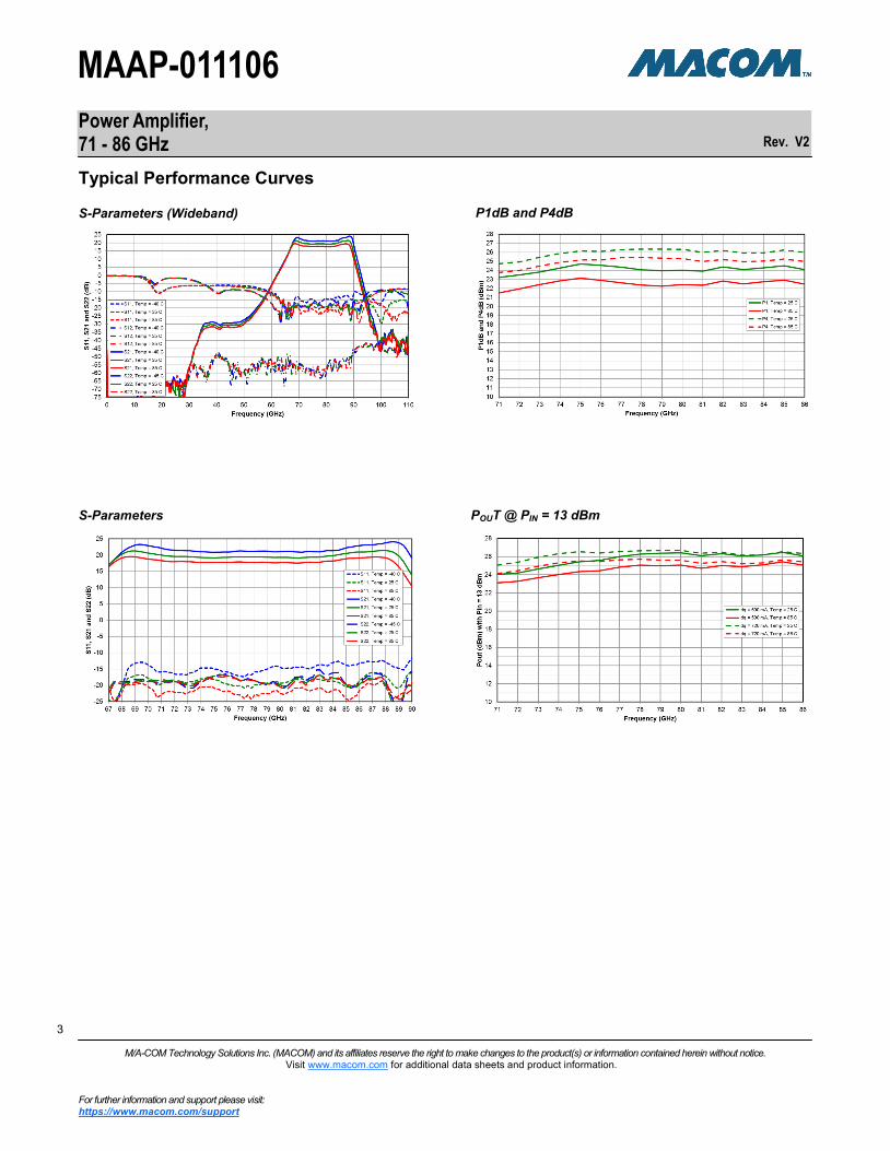
Typical Performance Curves
Worst Tone Output IP3 Lower and Upper Tone Gain, IIP3 and OIP3 vs. Current
S-Parameters @ 80 GHz vs. Current Detector Delta Voltage vs. Output Power
M/A-COM Technology Solutions Inc. (MACOM) and its affiliates reserve the right to make changes to the product(s) or information contained herein without notice. Visit www.macom.com for additional data sheets and product information.
For further information and support please visit: https://www.macom.com/support
5
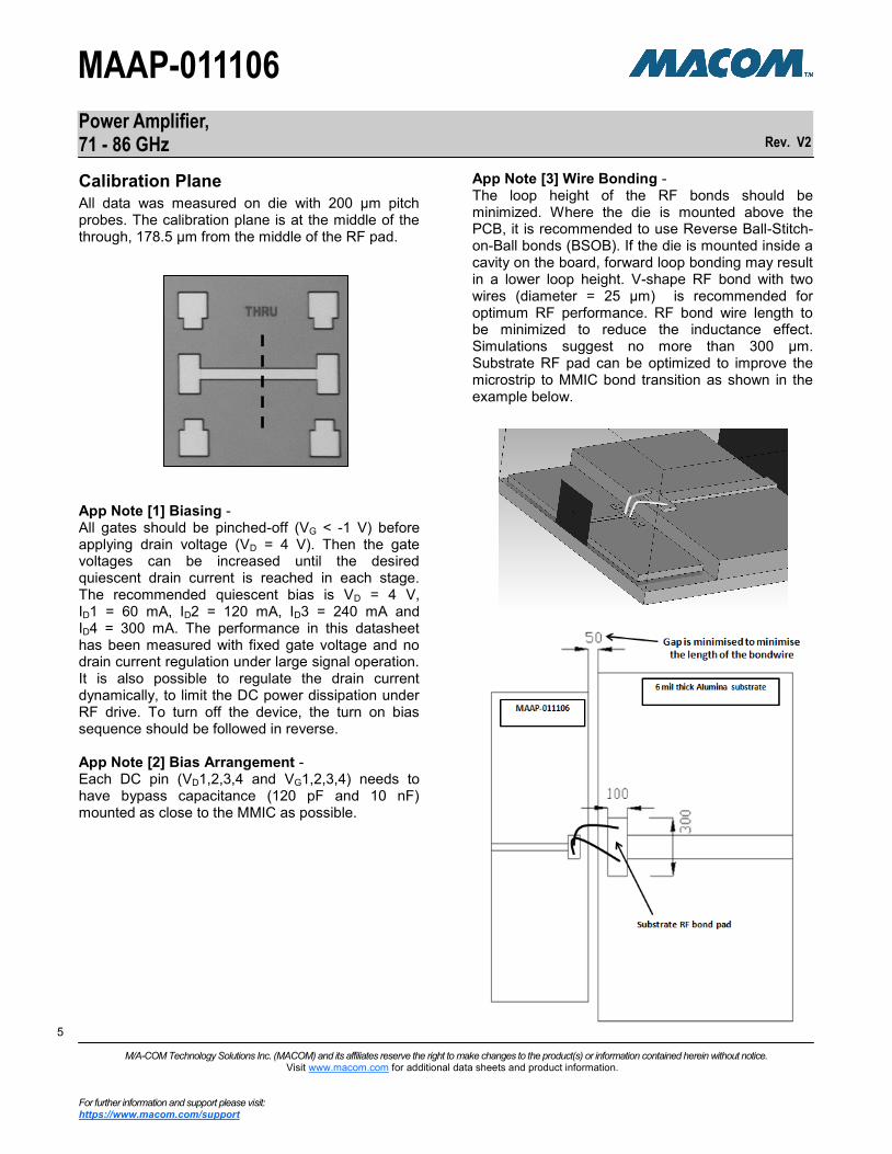
Calibration Plane
All data was measured on die with 200 µm pitch probes. The calibration plane is at the middle of the through, 178.5 µm from the middle of the RF pad.
App Note [1] Biasing - All gates should be pinched-off (VG < -1 V) before applying drain voltage (VD = 4 V). Then the gate voltages can be increased until the desired quiescent drain current is reached in each stage. The recommended quiescent bias is VD = 4 V, ID1 = 60 mA, ID2 = 120 mA, ID3 = 240 mA and ID4 = 300 mA. The performance in this datasheet has been measured with fixed gate voltage and no drain current regulation under large signal operation. It is also possible to regulate the drain current dynamically, to limit the DC power dissipation under RF drive. To turn off the device, the turn on bias sequence should be followed in reverse. App Note [2] Bias Arrangement - Each DC pin (VD1,2,3,4 and VG1,2,3,4) needs to have bypass capacitance (120 pF and 10 nF) mounted as close to the MMIC as possible.
App Note [3] Wire Bonding - The loop height of the RF bonds should be minimized. Where the die is mounted above the PCB, it is recommended to use Reverse Ball-Stitch-on-Ball bonds (BSOB). If the die is mounted inside a cavity on the board, forward loop bonding may result in a lower loop height. V-shape RF bond with two wires (diameter = 25 µm) is recommended for optimum RF performance. RF bond wire length to be minimized to reduce the inductance effect. Simulations suggest no more than 300 µm. Substrate RF pad can be optimized to improve the microstrip to MMIC bond transition as shown in the example below.
M/A-COM Technology Solutions Inc. (MACOM) and its affiliates reserve the right to make changes to the product(s) or information contained herein without notice. Visit www.macom.com for additional data sheets and product information.
For further information and support please visit: https://www.macom.com/support
6
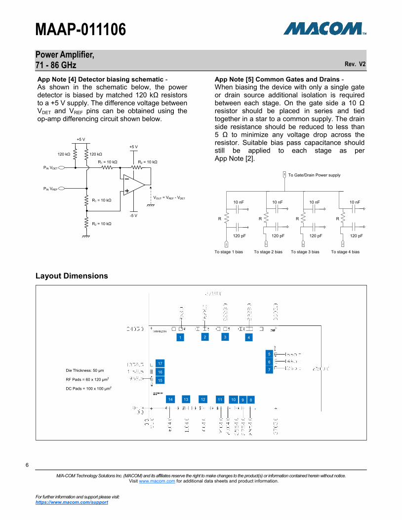
Layout Dimensions
App Note [4] Detector biasing schematic -
As shown in the schematic below, the power detector is biased by matched 120 kΩ resistors to a +5 V supply. The difference voltage between VDET and VREF pins can be obtained using the op-amp differencing circuit shown below.
Die Thickness: 50 µm RF Pads = 60 x 120 µm2 DC Pads = 100 x 100 µm2
App Note [5] Common Gates and Drains -
When biasing the device with only a single gate or drain source additional isolation is required between each stage. On the gate side a 10 Ω resistor should be placed in series and tied together in a star to a common supply. The drain side resistance should be reduced to less than 5 Ω to minimize any voltage drop across the resistor. Suitable bias pass capacitance should still be applied to each stage as per App Note [2].
1 2 3 4
5
6
7
8 9 10 11 12 13 14
15
16
17
To Gate/Drain Power supply
To stage 1 bias To stage 2 bias To stage 3 bias To stage 4 bias


![LCCH your family fro… · qam SDSdD 10 'ZLLZ -8£9-008-1 /ún(u! -POJd P pnpoJd lawnsu03 ayesun up uoclê] 'spnpold u! peal uo OL (DSdD) launsuo) u! peal 16Lþ-9ZV-008-L au!POH S,Vd3](https://static.documents.pub/doc/80x56/60230593d12a9f482f6edccb/your-family-fro-qam-sdsdd-10-zllz-89-008-1-nu-pojd-p-pnpojd-lawnsu03.jpg)


