Verilog Verilog Coding Coding REF: • Reuse Methodology Manual – For System-ON-A-Chip Design, Third Edition 2002 • CIC Training Manual – Logic Synthesis with Design Compiler, July, 2007 •Hsing-Chen, Lu, “ARES Lab 2008 Summer Training Course of V erilog Coding Style” • Hsi-Pin, Ma, “LARC Lab Training Course of Design Concept and Coding Style” 2010.12.01 Advanced Reliable Systems (ARES) Lab. 1
Transcript
VerilogVerilog CodingCodingREF: • Reuse Methodology Manual – For System-ON-A-Chip Design, Third Edition 2002• CIC Training Manual – Logic Synthesis with Design Compiler, July, 2007• Hsing-Chen, Lu, “ARES Lab 2008 Summer Training Course of Verilog Coding Style”s g C e , u, S ab 008 Su e a g Cou se o e og Cod g Sty e• Hsi-Pin, Ma, “LARC Lab Training Course of Design Concept and Coding Style”
16 instructions 16 instructions SRAM: 64 bytes (使用Artisan產生) Consists of an ALU, instruction decoder, and three 8-bit register files
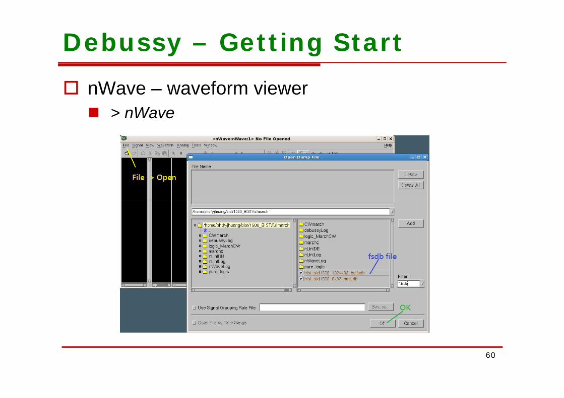
步驟二:使用編輯好的RTL netlist跑simulation,並觀察波形。
2
Cell-Based Design Flow
MATLAB/ C/ C++/ System C/ ADS/ Covergen (MaxSim)
Memory Generator
Spec.
System LevelADS/ Covergen (MaxSim)
NC-Verilog/ ModelSimDebussy (Verdi)/ VCS
Verilog/ VHDL SyntestRTL Level
Design/ Power Compiler
DFT Compiler/ TetraMAX
mpi
ler/
Fusi
on
Conformal/Formality
Logic Synthesis
Design for Test
NC-Verilog/ ModelSimDebussy (Verdi)/ VCS
hysi
cal C
omgm
a B
last
Gate Level
SOC Encounter/ Astro
DRC/ LVS (Calibre)
Ph Mag
GDS IILayout Level
Post-Layout Verification
PVS: Calibre xRC/ NanoSim(Time/ Power Mill)
Verification
Tape Out3
Basic Concept of Verilog HDLBasic Concept of Verilog HDL
4
Outline
Introduction to Verilog HDL l f b i Levels of Abstraction Module Format Verilog Syntax Example of Testbenches Example of Testbenches
5
Introduction to Verilog HDL
Verilog is a Hardware Description Language(HDL) h d d i i l i l d A hardware description language is a language used
to describe a digital system Why using an Hardware Describe Language? Design abstrac on: HDL ←→ layout by human Hardware modeling Reduce cost and time to design hardware
6
Verilog Model Key features of Verilog Supports various levels of abstraction Supports various levels of abstraction Switch level model or transistor level model Gate level model Data flow model or register transfer model Behavioral model
7
Gate Level Model (GTL) Model consists of basic logic Ex: AND,NAND,OR,NOR,BUF,NOT…etc., , , , ,
always@(posedge clk or posedge reset) beginif (reset)
out = 0;else if (enable)
out = out + 1;out = out + 1;end
endmodule
23
FSM Coding Style
Explicit FSM design always@(state or in)begin
case (state)case (state)S0:
if (in) next_state = S1;else next state = S0;else next_state S0;
S1:…
end
always@(posedge clk)if(~reset)
state <= S0;else
state <= next_state;
24
Example of Testbench
321
25
Example of Testbench (Cont’)
4 5
6
26
S th i bl V il C dSynthesizable Verilog Code
27
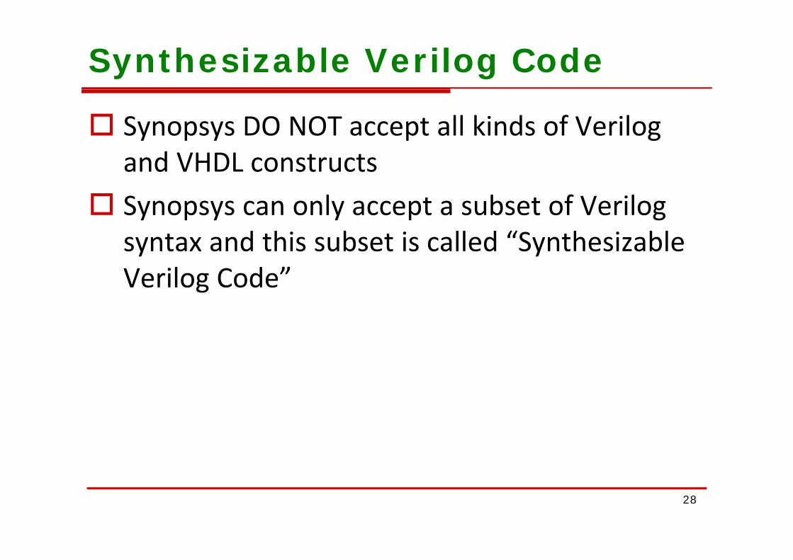
Synthesizable Verilog Code
Synopsys DO NOT accept all kinds of Verilogd VHDLand VHDL constructs
Synopsys can only accept a subset of Verilogy p y y p gsyntax and this subset is called “Synthesizable Verilog Code”Verilog Code
28
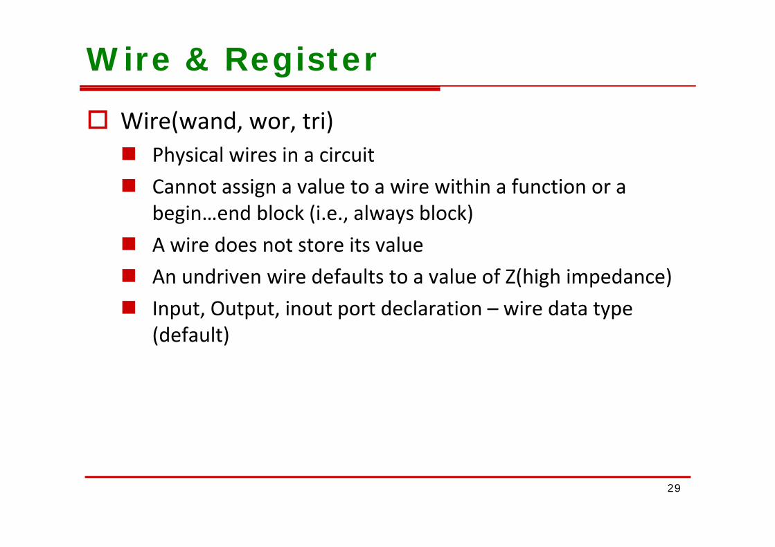
Wire & Register
Wire(wand, wor, tri) Ph i l i i i it Physical wires in a circuit Cannot assign a value to a wire within a function or a
begin end block (i e always block)begin…end block (i.e., always block) A wire does not store its value An undriven wire defaults to a value of Z(high impedance) An undriven wire defaults to a value of Z(high impedance) Input, Output, inout port declaration – wire data type
(default)(default)
29
Wire & Register (Cont’) reg: a variable in Verilog Use of “reg” data type is not exactly synthesized to a Use of reg data type is not exactly synthesized to a
really register Compare to use of wire & reg Compare to use of wire & reg
wire usually use “assign” and “assign” dose not appear in “always” block module test(a, b, c);
reg only use “a=b”, always appear in “always” block
input a,b;output c;
iwire c=a;reg c;
always@(a)beginalways@(a)beginc=a;
endendmodule
30
endmodule
Eliminate Glue Logic at the Top Level
Do not instantiate gate‐level logic at the top l l f h hi hlevel of the macro hierarchy
31
Concept of Clocks and Reset
Synchronous Mixed Clock Edges
QD D QCBLQD D QCBL
clk clk
Gated ClocksCombination FeedbackQD D Q
CBL
clk
32
Coding for Synthesis
Combinational Blocks Sequential Blocks
always @ (d) begincase (d)
2'b00: z=1'b1;
always @ (posedge clk ) begin
if (a) begin;2'b01: z=1'b0;default : z=1'b0;
endcase
z<=1’b1;endelse begin
end
always @ (a or x_temp)begin
z<=1’b0;end
endbegin
if (a) beginx= x_temp+1’b1;
endendelse begin
x= x_temp;end
33
end
Coding for Synthesis (Cont’)
Avoid Combinational Feedback
l @ ( d lk) b ialways @ (a or x)beginif (a) begin
x= x+1’b1;
always @ (posedge clk) beginx_temp<=x;
endendelse begin
x= x;d
always @ (a or x_temp)beginif (a) begin
x= x temp+1’b1;end x= x_temp+1 b1;endelse begin
x= x temp;x x_temp;end
34
Coding for Synthesis (Cont’)
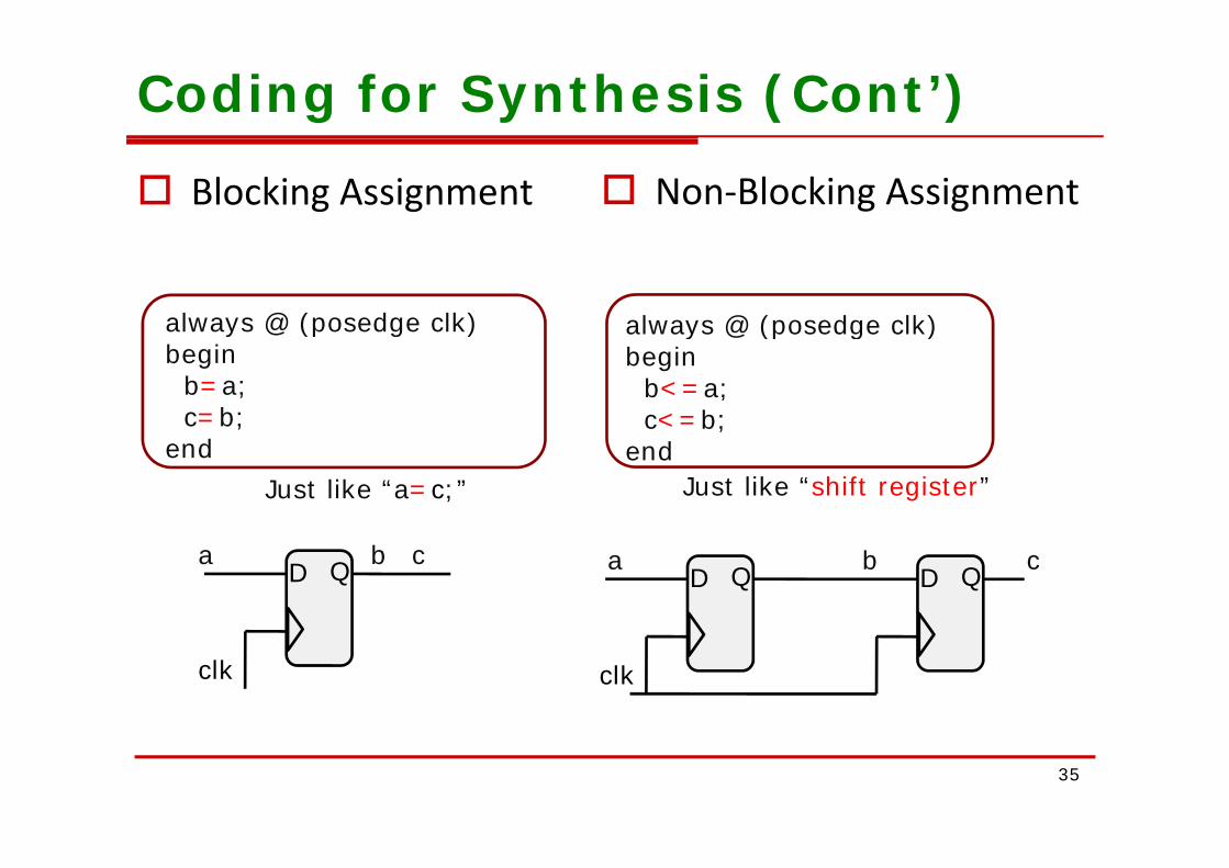
Blocking Assignment Non‐Blocking Assignment
always @ (posedge clk) always @ (posedge clk) y (p g )begin
b=a;c=b;
y @ (p g )begin
b<=a;c<=b;
end endJust like “a=c;” Just like “shift register”
QD QD D Qa b ca b c
clk clk
35
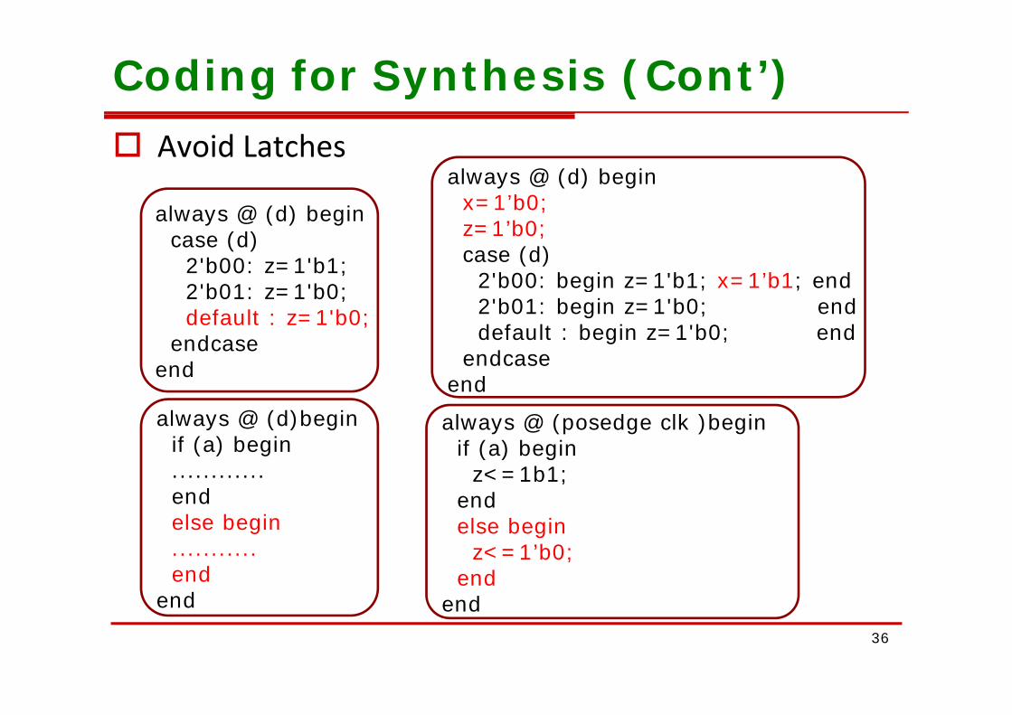
Coding for Synthesis (Cont’) Avoid Latches
always @ (d) begin1’b0always @ (d) begin
case (d)2'b00: z=1'b1;
x=1’b0;z=1’b0;case (d)
2'b00: begin z 1'b1; x 1’b1; end;
2'b01: z=1'b0;default : z=1'b0;
endcase
2'b00: begin z=1'b1; x=1’b1; end2'b01: begin z=1'b0; enddefault : begin z=1'b0; end
endcaseend
always @ (posedge clk )beginalways @ (d)beginif ( ) b i
endcaseend
if (a) beginz<=1b1;
endl b i
if (a) begin............endelse begin else begin
z<=1’b0;end
end
else begin...........end
end36
endend
Coding for Synthesis (Cont’)
Sensitivity List
always @ (d) begincase (d)
2'b00: z 1'b1;
always @ (a or b or c or d)beginif (a) begin
2 b00: z=1 b1;2'b01: z=1'b0;default : z=1'b0;
endcase
............endelse begin
if (b)beginendcaseend
if (b)beginz=c;
endelse beginelse begin
z=d;end
endend
37
Coding for Synthesis (Cont’)
Syntax error for Verilog Simulation Mixed edge‐triggered and level‐sensitive control in
an always block
always@(addr or posedge clk)begin
…dend
38
Coding for Synthesis (Cont’)
Key: The multiplexer is a faster circuit. If the i i di i i dpriority‐encoding structure is not required, we
recommend using the case statement Using a conditional assignment to infer a Mux assign out = sel ? a : b ; assign out = sel ? a : b ;
39
Conditional Expressions
If statement vs. Case statement If statement Priority‐encoded logic For speed critical path
Case statement Balanced logic For complex decodingo co p e decod g
40
Conditional Expressions (Cont’) Case statements if – else statements
Non-Synthesizable Style Either non‐synthesizable or incorrect after synthesis initial block is forbidden (non‐synthesizable) initial block is forbidden (non synthesizable) Multiple assignments (multiple driving sources)
( th i bl )(non‐synthesizable) always@(src1 or src2)result = src1 + src2;
always@(src1 or src2 or inc)begin…d 1 2des = src1 + src2;inc <= src1-4;…end
42
end
Tips for Verilog Design
Resource Sharing Scalable Design Using ( ) to describe complex circuits Using ( ) to describe complex circuits Timescale
43
Resource Sharing
Operations can be shared if they lie in the l bl k
Al @ ( l b )
same always block
Always @ (sel or a or b or c )begin
if (sel) z=a+b;else z=a+c;
end
44
Scalable Design
parameter size=8;[ ] b dwire [3:0] a,b,c,d,e;
assign a=size+2;assign b=a+1;
ConstantIncreaserAddassign c=d+e; Adder
45
Omit for Synthesis
Omit the Wait for XX ns Statement Do not use “#XX;”
Omit the ...After XX ns or Delay Statement Omit the ...After XX ns or Delay Statement Do not use “assign #XX Q=0;”
O i I i i l V l Omit Initial Values Do not use “initial sum = 1’b0;”
46
Using ( ) to describe complex circuits.
out=a+b+c+d+e; out=((a+(b+c))+(d+e));
a b
c bc
d
c
a d ed
ee
outout
47
Timescale `timescale: which declares the time unit and precision.
`timescale <time unit> / <time precision>_ / _p e.g. : `timescale 1s/1ps, to advance 1 sec, the timewheel scans its
queues 1012 times versus a `timescale 1s/1ms, where it only scans the queues 103 timesthe queues 103 times.
The time_precision must be at least as precise as the time unittime_unit
Keep precision as close in scale to the time units as is practicalp
If not specified, the simulator may assign a default timescale unit
The smallest precision of all the timescale directive determines the “simulation time unit ” of the simulation.
48
Summary No initial in the RTL code FFs are preferred FFs are preferred Avoid unnecessary latches Avoid combinational feedback For sequential blocks, use no‐blocking statements For combinational blocks, use blocking statements Coding state machines Coding state machines Two procedure blocks: one for the sequential and one for the
combinationalcombinational Keep FSM logic and non‐FSM logic in separate modules Assign a default state Assign a default state
49
Artisan Memory CompilerArtisan Memory Compiler
50
Getting Started linux %> ssh ‐l “user name” cae18.ee.ncu.edu.tw(1‐port RAM) unix%> ~/cell_lib/CBDK018_TSMC_Artisan/CIC/Memory/ra1shd/bin/ra1shd