SANDIA REPORT SAND2009-6086 Unlimited Release Printed September 2009 Vibrational Spectra of Nanowires Measured Using Laser Doppler Vibrometry and STM Studies of Epitaxial Graphene: An LDRD Fellowship Report Laura B. Biedermann Prepared by Sandia National Laboratories Albuquerque, New Mexico 87185 and Livermore, California 94550 Sandia is a multiprogram laboratory operated by Sandia Corporation, a Lockheed Martin Company, for the United States Department of Energy’s National Nuclear Security Administration under Contract DE-AC04-94-AL85000. Approved for public release; further dissemination unlimited.
Transcript
SANDIA REPORTSAND2009-6086Unlimited ReleasePrinted September 2009
Vibrational Spectra of NanowiresMeasured Using Laser DopplerVibrometry andSTM Studies of Epitaxial Graphene:An LDRD Fellowship Report
Laura B. Biedermann
Prepared bySandia National LaboratoriesAlbuquerque, New Mexico 87185 and Livermore, California 94550
Sandia is a multiprogram laboratory operated by Sandia Corporation,a Lockheed Martin Company, for the United States Department of Energy’sNational Nuclear Security Administration under Contract DE-AC04-94-AL85000.
Approved for public release; further dissemination unlimited.
Issued by Sandia National Laboratories, operated for the United States Department of Energyby Sandia Corporation.
NOTICE: This report was prepared as an account of work sponsored by an agency of the UnitedStates Government. Neither the United States Government, nor any agency thereof, nor anyof their employees, nor any of their contractors, subcontractors, or their employees, make anywarranty, express or implied, or assume any legal liability or responsibility for the accuracy,completeness, or usefulness of any information, apparatus, product, or process disclosed, or rep-resent that its use would not infringe privately owned rights. Reference herein to any specificcommercial product, process, or service by trade name, trademark, manufacturer, or otherwise,does not necessarily constitute or imply its endorsement, recommendation, or favoring by theUnited States Government, any agency thereof, or any of their contractors or subcontractors.The views and opinions expressed herein do not necessarily state or reflect those of the UnitedStates Government, any agency thereof, or any of their contractors.
Printed in the United States of America. This report has been reproduced directly from the bestavailable copy.
Available to DOE and DOE contractors fromU.S. Department of EnergyOffice of Scientific and Technical InformationP.O. Box 62Oak Ridge, TN 37831
A few of the many applications for nanowires are high-aspect ratio conductive atomic force micro-scope (AFM) cantilever tips, force and mass sensors, and high-frequency resonators. Reliable esti-mates for the elastic modulus of nanowires and the quality factor of their oscillations are of interestto help enable these applications. Furthermore, a real-time, non-destructive technique to measurethe vibrational spectra of nanowires will help enable sensor applications based on nanowires andthe use of nanowires as AFM cantilevers (rather than as tips for AFM cantilevers).
Laser Doppler vibrometry is used to measure the vibration spectra of individual cantileverednanowires, specifically multiwalled carbon nanotubes (MWNTs) and silver gallium nanoneedles.Since the entire vibration spectrum is measured with high frequency resolution (100 Hz for a10 MHz frequency scan), the resonant frequencies and quality factors of the nanowires are accu-rately determined. Using Euler-Bernoulli beam theory, the elastic modulus and spring constant canbe calculated from the resonance frequencies of the oscillation spectrum and the dimensions of thenanowires, which are obtained from parallel SEM studies. Because the diameters of the nanowires
3
studied are smaller than the wavelength of the vibrometer’s laser, Mie scattering is used to estimatethe lower diameter limit for nanowires whose vibration can be measured in this way. The tech-niques developed in this thesis can be used to measure the vibrational spectra of any suspendednanowire with high frequency resolution
Two different nanowires were measured–MWNTs and Ag2Ga nanoneedles. Measurements ofthe thermal vibration spectra of MWNTs under ambient conditions showed that the elastic mod-ulus, E, of plasma-enhanced chemical vapor deposition (PECVD) MWNTs is 37±26 GPa, wellwithin the range of E previously reported for CVD-grown MWNTs. Since the Ag2Ga nanoneedleshave a greater optical scattering efficiency than MWNTs, their vibration spectra was more exten-sively studied. The thermal vibration spectra of Ag2Ga nanoneedles was measured under bothambient and low-vacuum conditions. The operational deflection shapes of the vibrating Ag2Gananoneedles was also measured, allowing confirmation of the eigenmodes of vibration. The mod-ulus of the crystalline nanoneedles was 84.3±1.0 GPa.
Gas damping is the dominate mechanism of energy loss for nanowires oscillating under ambi-ent conditions. The measured quality factors, Q, of oscillation are in line with theoretical predic-tions of air damping in the free molecular gas damping regime. In the free molecular regime, Qgasis linearly proportional to the density and diameter of the nanowire and inversely proportional tothe air pressure. Since the density of the Ag2Ga nanoneedles is three times that of the MWNTs,the Ag2Ga nanoneedles have greater Q at atmospheric pressures. Our initial measurements of Qfor Ag2Ga nanoneedles in low-vacuum (10 Torr) suggest that the intrinsic Q of these nanoneedlesmay be on the order of 1000.
The epitaxial carbon that grows after heating (0001) silicon carbide (SiC) to high tempera-tures (1450–1600) in vacuum was also studied. At these high temperatures, the surface Si atomssublime and the remaining C atoms reconstruct to form graphene. X-ray photoelectron spec-troscopy (XPS) and scanning tunneling microscopy (STM) were used to characterize the qual-ity of the few-layer graphene (FLG) surface. The XPS studies were useful in confirming thegraphitic composition and measuring the thickness of the FLG samples. STM studies revealed awide variety of nanometer-scale features that include sharp carbon-rich ridges, moire superlattices,one-dimensional line defects, and grain boundaries. By imaging these features with atomic scaleresolution, considerable insight into the growth mechanisms of FLG on the carbon-face of SiC isobtained.
4
Acknowledgment
This SAND report is a summary of my graduate research, which was supported by Sandia Na-tional Laboratories through the Purdue Excellence in Science and Engineering Fellowship fromAugust 2005 through May 2009. Throughout this fellowship, Dr. Steve Howell of Sandia NationalLaboratories provided invaluable guidance.
This research, a five-year collaborative effort, was undertaken at Purdue University. First andforemost, I would like to thank my advisor, Professor Ron Reifenberger, for his guidance, wisdom,and humor. When that “great thing called Google” failed, Ron was always there with advice.When the experiments were successful, interesting, or puzzling, I appreciated his insight into howto improve the experiments and explain the results. When the experiments were disappointing, Iwas immensely grateful to him for his encouragement.
Professor Arvind Raman has graciously served as an unofficial second advisor the past fewyears. He has been an enthusiastic collaborator in the measurements of the vibrational spectra ofnanowires. I have appreciated working with all of his graduate students, whom have been fabulouscollaborators and friends. First, all of the vibrometer measurements of carbon nanotube spectrawere done in collaboration with Ryan Tung. Bill Conley and Mark Strus provided insight into theproperties of carbon nanotubes. Much of my understanding of cantilever dynamics comes fromreading papers and attending presentations by John Melcher as well as many hours of conversationswith John. Ryan Wagner assisted with the Sader’s method calculations. Jose Lozano is thankedfor his advice concerning thermally-excited cantilevers and the fluctuation-dissipation theorem.
As this SAND report is a summary of my graduate research, I would like to thank the membersof my thesis committee, Professor Erica Carlson, Dr. Steve Howell, and Professor Ken Ritchie fortheir experimental advice as well as for being excellent role models and teachers.
I have been fortunate to meet a number of inspiring collaborators. Dr. Mehdi Yazdanpanahof the University of Louisville provided the silver gallium nanoneedles whose vibrational spectand operational deflection shape were measured. Professor Michael Capano, Michael Bolen, andSara Harrison were instrumental collaborators in the study of epitaxial graphene as they grewall the samples studied and contributed to the analysis. I thank Dr. Dima Zemlyanov for his x-ray photoemission spectroscopy analysis of the graphene samples. Gyan Prakash’s atomic forcemicroscopy studies of the same graphene samples were very illuminating.
I would especially like to thank Mark Smith and Dr. Bob Santini for their electronics advicefor the tunnel gap modulation spectroscopy project. While that experiment was not successful, Iwill always appreciate their kind assistance and remember their advice.
My labmates have been wonderful sources of support, encouragement, advice, laughter, and
5
spare hands over the past five years. I would like to thank Babita Dhayal, Roya Lahiji, Chun Lan,Deepak Pandey, Gyan Prakash, Yexian Qin, Joel Therrien, and Steve Tripp,
Finally, I thank my mom and dad for their years of support, including letting me solder elec-tronics in the living room and study vibrational modes with sand in the kitchen. I am very luckyto have such encouraging parents. Last, but not least, I owe more thanks than I can express to myloving husband, Eric. Eric literally went the extra mile to support me throughout my PhD.
Studies of the epitaxial graphene growth were supported by the Indiana 21st Century Fund.
3.3 The non-dimensionalized fluid damping coefficients are plotted for the three can-tilevers for the case of free molecular (·), cross-over (o), and continuum (+) flowregimes. . . . . . . . . . . . . . . . . . . . . . . . . . . . . . . . . . . . . . . . . . . . . . . . . . . . . . . . . . . . 42
4.1 In (a), a schematic of the Polytec LDV used in this work. In (b), a schematicdiagram of a cantilevered nanowire. The reflected light (R) of the normally incidentlaser beam (I) is Doppler shifted by frequency ∆ when reflected from the MWNT.In (c), an illustration of the relative dimensions when the object beam is focusedthrough the 50× objective. As indicated by the shaded region, the beam waist ismuch wider than the nanowire. . . . . . . . . . . . . . . . . . . . . . . . . . . . . . . . . . . . . . . . . . 44
4.2 In (a), an SEM of the 16.6 µm long, 140 nm diameter nanoneedle NNB2. Two redcircles, diameter 0.9 µm, indicate the spot size of the laser. In (b), the measuredODS and theoretical first eigenmode, both normalized. The laser return at the tip-most point on the nanoneedle was poor; for this reason the last data point under-estimates the displacement amplitude. . . . . . . . . . . . . . . . . . . . . . . . . . . . . . . . . . . . . 45
4.3 (a) The FRF of a Si3N4 cantilever, as measured using the Nanotec AFM. (b) Thepower spectral density measured using the LDV for the same cantilever. . . . . . . . . . 47
4.5 The calculated Qsca for circularly polarized 633 nm light normally incident ona cylindrical nanowire in air as a function of diameter. In (a), the case of lightscattering off of metallic silver and graphitic nanowires. The diameters of MWNTsstudied fall within the range indicated by the dashed vertical lines. In (b), the caseof light scattering off of a semiconducting silicon nanowire. . . . . . . . . . . . . . . . . . . 53
12
5.1 In (a), a schematic of the experimental set-up for electrostatic excitation of aMWNT. In (b), the electrostatic excitation of MWNT A7a−9 at resonance. . . . . . . 56
5.2 The E calculated for seven PECVD-MWNTs based on the resonant frequenciesmeasured in the electrostatic excitation experiments. . . . . . . . . . . . . . . . . . . . . . . . . 57
5.3 In (a), the displacement frequency spectrum from MWNT NT1 shows eigenmodepeaks attributed to the 1st and 2nd bending modes of the MWNT. In (b), an SEMmicrograph of the MWNT affixed to the Ni tip. . . . . . . . . . . . . . . . . . . . . . . . . . . . . 59
5.4 A series of 50× darkfield images showing the transfer of a gold-coated glass beadto a MWNT. . . . . . . . . . . . . . . . . . . . . . . . . . . . . . . . . . . . . . . . . . . . . . . . . . . . . . . . . 60
5.5 In (a), the velocity spectrum of a MWNT showing a vibration peak at 53.3 kHz thatis attributed to the bending oscillation of the MWNT. In (b), an SEM micrographof the MWNT with gold-coated glass bead affixed to the MWNT tip. . . . . . . . . . . . 61
5.6 In (a), an SEM micrograph of NNB. (b) The 1st through 4th eigenfrequencies areobserved in the velocity PSD. (c) The displacement PSD shows the 2nd through 9th
eigenfrequencies. In (d), the measured ODS of the eighth eigenmode. . . . . . . . . . . . 65
5.7 In (a) and (b), log-log plots of the power spectra densities of NND and NNE,respectively, show a flat frequency response below ∼1 MHz. In (c) and (d), SEMmicrographs of NND and NNE, respectively. . . . . . . . . . . . . . . . . . . . . . . . . . . . . . . 68
5.8 In (a) and (b), SEM micrographs of nanoneedle B2 show two parallel nanoneedles,16.6 µm and 17 µm long. In (c), an illustration of the cross-sectional area. . . . . . . . 70
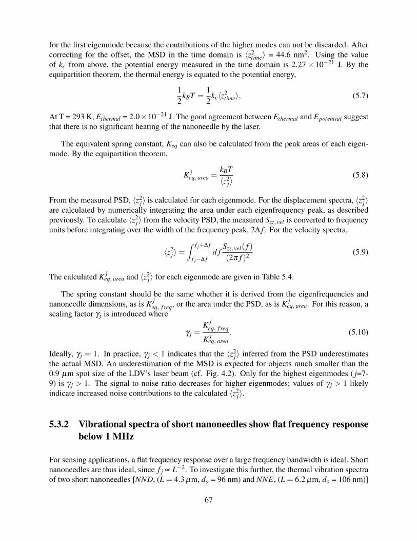
5.9 The vibrational spectra of nanoneedle pair NNB2 shows two first eigenfrequencypeaks at f1,a = 0.22 MHz and f1,b = 0.46 MHz and two second eigenfrequencypeaks at f2,a = 1.42 MHz and f2,b = 2.79 MHz. . . . . . . . . . . . . . . . . . . . . . . . . . . . . 71
5.10 The optical forcing on a Ag nanowire from a 633 nm, 1 mW Gaussian laser beamas a function of nanowire diameter. . . . . . . . . . . . . . . . . . . . . . . . . . . . . . . . . . . . . . . 74
5.11 A 50× optical microscope image of nanoneedle NNF (do=65 nm, L=21.5 µm),bent ∆ = 2 µm away from the equilibrium position due to the optical forcing. . . . . . 75
5.12 (a) The time series measurement of the fundamental ( j=1) oscillations of NNBshows sinusoidal oscillations with an amplitude of ∼25 nm and a beat frequencyof 2.0 kHz. In (b), the Fourier transform of the time series signal has two low-frequency peaks at 29.9 kHz and 31.9 kHz. . . . . . . . . . . . . . . . . . . . . . . . . . . . . . . . . 76
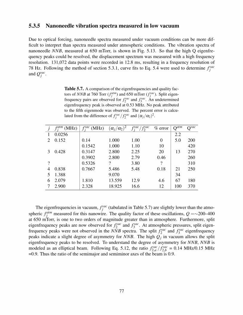
5.13 (a) The thermal spectra of nanoneedle NNB, measured at 650 mTorr, shows f2–f4, f6, and f7. In (b) the split eigenfrequency peaks f vac
2 and f vac3 are visible in
this smaller frequency range. Inset (c) highlights the high quality factor of thesevibrations, Qvac
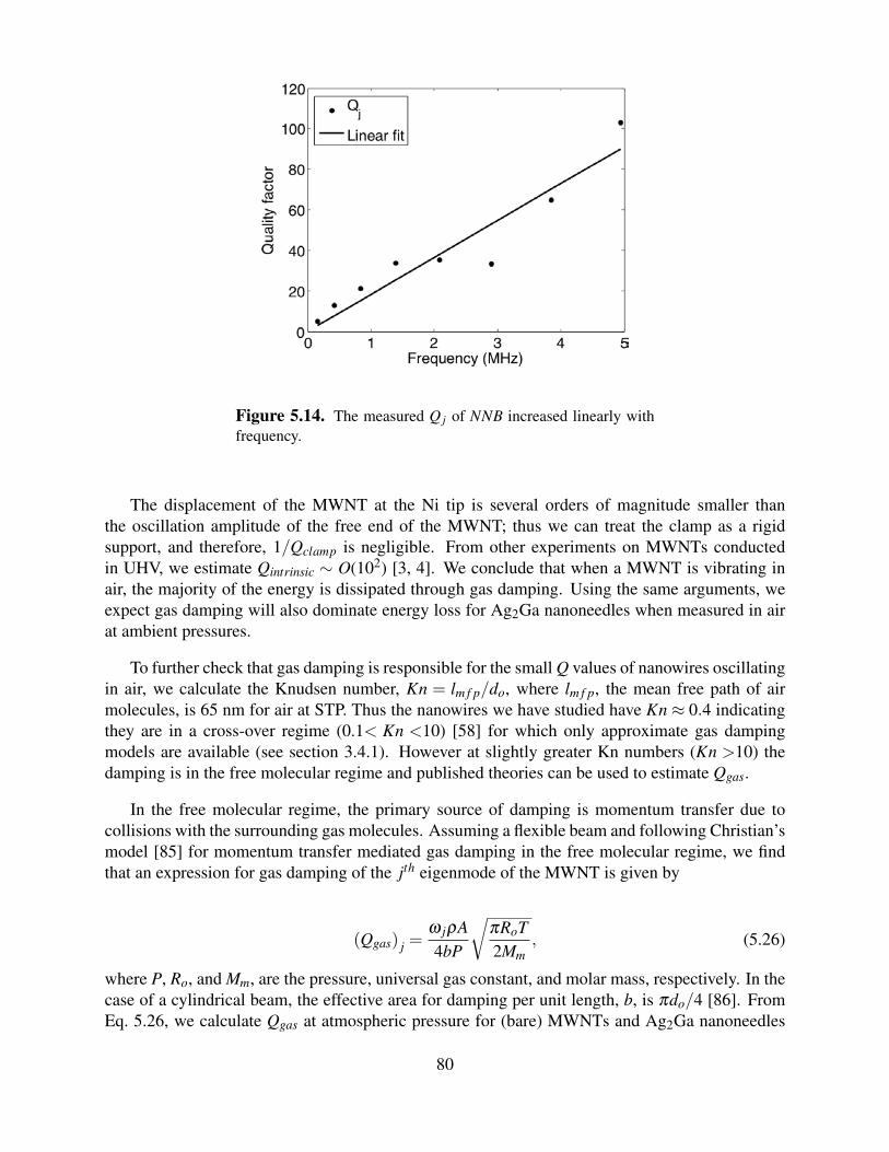
5.14 The measured Q j of NNB increased linearly with frequency. . . . . . . . . . . . . . . . . . . 80
5.15 The calculated Qgas for nanowires oscillating at atmospheric pressure, using thecalculations of the free molecular flow regime. Qgas is calculated for Ag2Gananoneedles (red) and MWNTs (blue) of representative diameters. Measured Qmeascorresponding to the first eigenmode of vibration are superimposed on the calcu-lated Qgas . . . . . . . . . . . . . . . . . . . . . . . . . . . . . . . . . . . . . . . . . . . . . . . . . . . . . . . . . . 81
7.1 In the Bernal stacking of HOPG (a), the layers alternate ABAB. (b) A rotationof the top graphene layer of the HOPG can lead to AAB, slip B, or BAB stackingsequences. . . . . . . . . . . . . . . . . . . . . . . . . . . . . . . . . . . . . . . . . . . . . . . . . . . . . . . . . . 92
7.2 The C-1s XPS spectra, collected at θ = 0o, from a reference HOPG substrate (a)and from a FLG sample grown at 1500C on SiC (b). The similarity of the twoXPS spectra indicates the presence of graphitic carbon on SiC. A closer exam-ination of the region between 288 eV and 295 eV from both samples providesevidence for shake-up satellites. . . . . . . . . . . . . . . . . . . . . . . . . . . . . . . . . . . . . . . . . 96
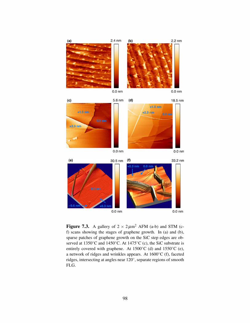
7.3 A gallery of 2 × 2 µm2 AFM (a-b) and STM (c-f) scans showing the stages ofgraphene growth at temperatures 1350C–1600C. . . . . . . . . . . . . . . . . . . . . . . . . . . 98
7.4 Two examples of ridges surrounding pits in the substrate. In (a), a 2 × 2 µm2
region showing a small pit completely surrounded by ridges (sample 927). In (b) a7.5× 7.5 µm2 region showing the highest ridge density observed on these epitaxialgraphene samples (sample 976). . . . . . . . . . . . . . . . . . . . . . . . . . . . . . . . . . . . . . . . . 99
7.6 STM images of a region from the graphene grown at 1500C show a parallel 1Dfeatures within a grain boundary in rough graphene. . . . . . . . . . . . . . . . . . . . . . . . . . 101
7.7 An STM image of a 200 × 200 nm2 region shows a 1D superlattice. . . . . . . . . . . . . 102
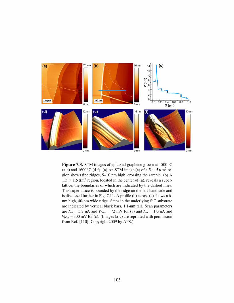
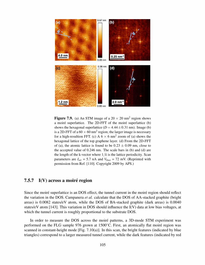
7.9 (a) An STM image of a 20 × 20 nm2 region shows a moire superlattice with D =4.44± 0.31 nm. (c) A 6 × 6 nm2 zoom of (a) shows the hexagonal lattice of thetop graphene layer. The 2D-FFTs of (a) and (c) are given in (b) and (d), respectively.105
7.10 (a) A constant-height STM scan of a 14.5 × 14.5 nm2 region with a moire super-lattice having a periodicity of 4.8± 0.3 nm (Vbias = 300 mV). In (b), a 3D-modeSTM scan of the same superlattice region. In the low-bias (±50 mV) range, theI(V)s (c) obtained from the 3D-mode STM scan in (b) are linear. . . . . . . . . . . . . . . . 106
14
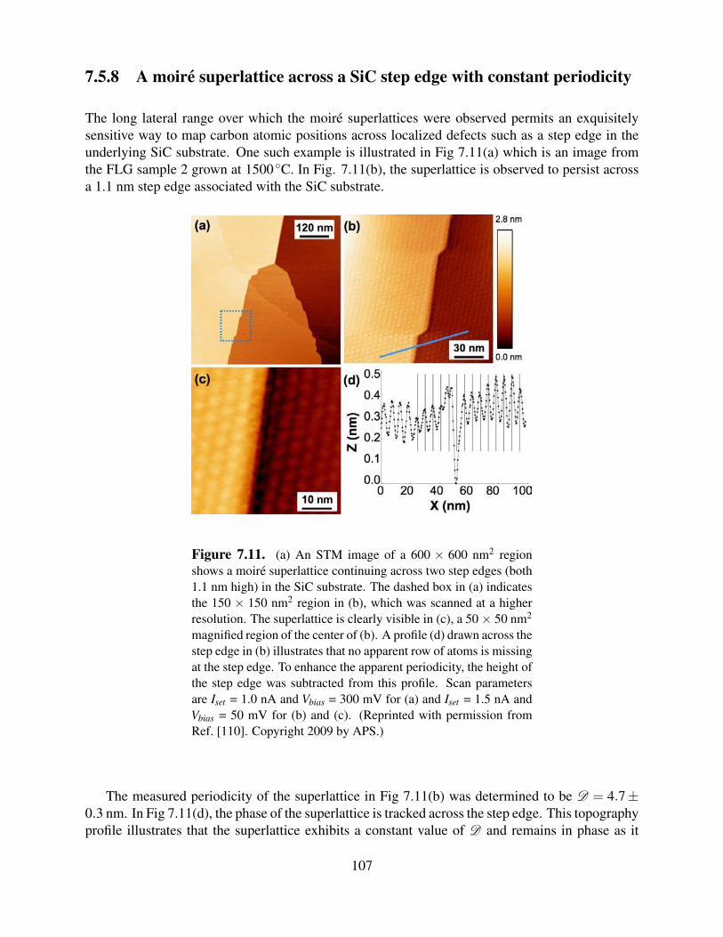
7.11 (a) and (b) STM images show a moire superlattice continuing across 1.1-nm highstep edges in the SiC substrate. The superlattice is clearly visible in (c), a 50 ×50 nm2 magnified region of the center of (b). A profile (d) drawn across the stepedge in (b) illustrates that no apparent row of atoms is missing at the step edge. . . 107
7.12 (a) An STM image (1000 × 700 nm2) shows the extent of the moire region witha periodicity of D = 12.7± 2.1 nm. The exceptionally jagged edge of the moireregion is illustrated by a 350 × 250 nm2 inset. . . . . . . . . . . . . . . . . . . . . . . . . . . . . . 108
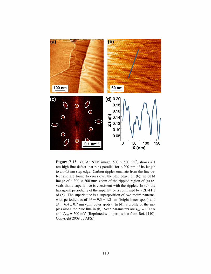
7.13 (a) An STM image, 500× 500 nm2, shows a 1 nm high line defect. Carbon ripplesemanate from the line defect and cross over the step edge. In (b), an STM imageof a 300 × 300 nm2 zoom of the rippled region of (a) reveals that a superlattice iscoexistent with the ripples. In (c), the hexagonal periodicity of the superlattice isconfirmed by a 2D-FFT of (b). In (d), a profile of the ripples. . . . . . . . . . . . . . . . . . 110
3.1 Allowed α j which correspond to the first five oscillation frequencies. . . . . . . . . . . . 34
4.1 Potential energy of a Si3N4 cantilever, using 〈z2f req〉 = 0.0094 nm2 and K1
eq =α4
1 kc/12. The Q is determined from the curve fit to either the AFM or LDV data. . 49
5.1 Experimentally measured elastic modulus for the MWNTs studied. The calcula-tions in this table assume di = 0.5do. The estimated estimated errors are ±10 nmfor do, ±0.2 µm for L, and ±2 kHz for f j. . . . . . . . . . . . . . . . . . . . . . . . . . . . . . . . . 58
5.2 Experimentally measured elastic modulus for MWNTs with beads. The calcula-tions in this table assume di = 0.5do. The estimated estimated errors are ±10 nmfor do, ±0.2 µm for L, and ±2 kHz for f j. Bead diameters (not listed, estimatederror ±20 nm) were measured in the FESEM and used to estimate the mass of thebead. . . . . . . . . . . . . . . . . . . . . . . . . . . . . . . . . . . . . . . . . . . . . . . . . . . . . . . . . . . . . . . 61
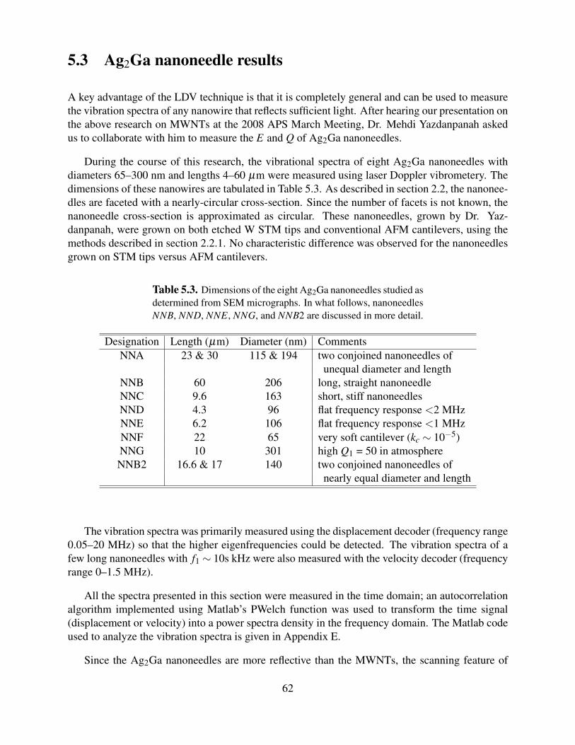
5.3 Dimensions of the eight Ag2Ga nanoneedles studied as determined from SEMmicrographs. In what follows, nanoneedles NNB, NND, NNE, NNG, and NNB2are discussed in more detail. . . . . . . . . . . . . . . . . . . . . . . . . . . . . . . . . . . . . . . . . . . . 62
5.4 The measured eigenfrequencies, f j, of NNB and mean square displacements, z2j ,
of the 1st–9th eigenmodes, as determined from both the velocity and displacementspectra. The percent error is calculated from the frequency ratios. The scalingfactor γ j is calculated from Eq. 5.10. . . . . . . . . . . . . . . . . . . . . . . . . . . . . . . . . . . . . . 66
5.5 The measured eigenfrequencies and quality factors of nanoneedles NND and NNE.Only a single second eigenfrequency above the noise floor was observed for NNE. 68
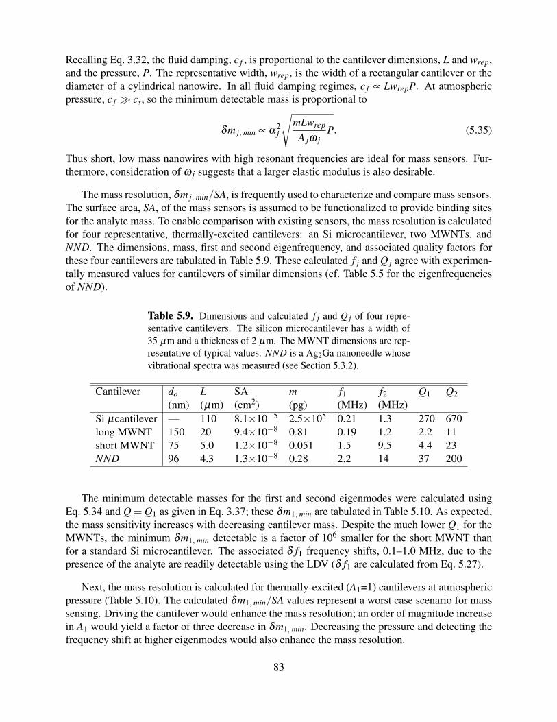
5.9 Dimensions and calculated f j and Q j of four representative cantilevers. The siliconmicrocantilever has a width of 35 µm and a thickness of 2 µm. The MWNT di-mensions are representative of typical values. NND is a Ag2Ga nanoneedle whosevibrational spectra was measured (see Section 5.3.2). . . . . . . . . . . . . . . . . . . . . . . . . 83
7.1 Five C-face epitaxial graphene samples were studied in depth with STM and AFM.Only AFM scans are presented for samples 924 and 926, which had incompletegraphene coverage. The growth temperatures and figures acquired from these sam-ples are tabulated below. . . . . . . . . . . . . . . . . . . . . . . . . . . . . . . . . . . . . . . . . . . . . . . 95
7.2 Samples with moire superlattice regions and their measured periodicity . . . . . . . . . 104
17
Preface
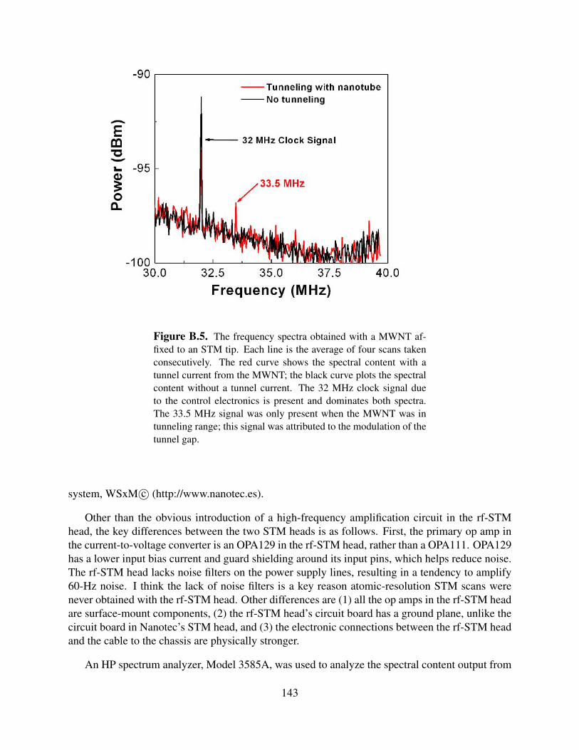
I joined the Reifenberger Nanophysics lab at Purdue University in January 2005 with the goal ofdesigning a custom scanning tunneling microscope (STM) to measure high frequency oscillationsin the tunnel current. In 2004 Dr. Joel Therrien, a post-doc in the Reifenberger lab, had conceivedof such an STM to measure the oscillations of nanoscale objects, such as multilwalled carbonnanotubes (MWNTs), placed in the tunnel gap of the STM. Joel’s early data suggested that thevibrations of the carbon nanotubes, ∼1 nm at 10s of MHz, could be measured by monitoring thetunnel current. I worked to both repeat Joel’s results and to design a custom STM head to improvethe amplification of the high-frequency signals in the tunnel current. As a short summary, I wasnot able to replicate Joel’s results; this effort is described in Appendix B: Tunnel Gap ModulationSpectroscopy (TGMS).
From the TGMS project, I did learn (1) the theory of nanowire oscillations, (2) how to pre-pare cantilevered MWNT samples, and (3) scanning tunneling microscopy, three skills which Ihave used throughout my degree. At the 2008 APS March Meeting, I presented a talk describingour measurements of MWNT flexural vibration spectra. This talk led to a collaboration with Dr.Mehdi Yazdanpanah and Prof. Robert Cohn of the University of Louisville. Dr. Yazdanpanah haddiscovered how to fabricate silver gallium nanoneedles on scanning probe microscope tips, butlacked a facile, non-destructive way to determine their elastic modulus. Using our laser Dopplervibrometery technique, we were able to measure the thermal and driven vibration spectra of thesesilver gallium nanoneedles and determine their elastic modulus.
My prior STM experience, as well as a long-standing interest in graphene, led me to join aPurdue graphene collaboration in October 2007. I provided STM analysis of epitaxial graphenegrown on silicon carbide. This fruitful collaboration, primarily between electrical engineers andphysicists at the Birck Nanotechnology Center, has led to insights into the nature of the graphenegrowth on the carbon-face of SiC.
The results of these projects to measure the vibrational spectra of nanowires, as well as theSTM studies of graphene, are presented in this SAND report.
18
Nomenclature
AFM Atomic force microscopy
CNT Carbon nanotube
CVD Chemical vapor deposition
FLG Few-layer graphene
FRF Frequency response function (linear response function)
LDV Laser Doppler vibrometry
ML Monolayer
MWNT Multiwalled carbon nanotube
MSD Mean square displacement
ODS Operating deflection shape
PECVD Plasma-enhanced chemical vapor deposition
PSD Power spectral density
SEM Scanning electron microscopy
SPM Scanning probe microscopy
STM Scanning tunneling microscopy
TEM Transmission electron microscopy
TGMS Tunnel gap modulation spectroscopy
XPS X-ray photoemission spectroscopy
19
20
Chapter 1
Introduction
Current commercial applications for nanowires include probe tips for atomic force microscope(AFM) cantilevers and the use of nanowires as stiffening elements in polymer matrices. Potentially,nanowires may be incorporated into vibrating nanomechanical systems (NEMS) such as ultra-highfrequency resonators, force and mass sensors, and nanoelectronics. A challenge limiting the useof nanowires in NEMS is that few methods exist to reliably measure their motion. A real-timetechnique capable of measuring the vibration of an individual nanowire would enable the designof sensitive chemical sensors and the use of nanowires as oscillators in nanomechanical systems.Of interest are the resonant frequencies of various eigenmodes of oscillation, the quality factorcharacterizing each resonant eigenmode, and the nanowire material properties required to explaineach resonance.
As carbon nanotubes (CNTs) are one of the most extensively studied nanowires, number ofmethods to determine the resonant frequency of a CNT have been published. Electrically excitedresonant vibrations of a cantilevered multiwalled carbon nanotube (MWNT) were observed in atransmission electron microscope (TEM) [1] and from the field emission pattern of a vibratingMWNT [2]. The oscillation of a suspended, doubly clamped MWNT, excited using an oscillatinggate voltage, was detected from the modulation in the conductance of the suspended device [3, 4].The shape of the first three bending eigenmodes of a suspended, doubly clamped MWNT wasmeasured using an AFM [5].
A number of the above techniques have been adopted to measure the resonant frequency ofother nanowires. For example, parametric resonance of boron nanowires has been observed inSEM [6]. Driven resonances of composite SiO2/SiC nanowires have been observed in TEM [7].Electrostatic actuation and piezoresistive self-detection has been used to detect driven resonanceof clamped-clamped Si nanowire resonators [8].
These techniques require either high vacuum conditions, electron microscopy, or complicatedfabrication methods that utilize advanced lithographic techniques. A feature common to all thesemethods is the low frequency resolution that accompanies the measurement of the nanowire vi-bration spectrum. We have used laser Doppler interferometry to measure the vibration spectra ofnanowires with high frequency resolution.
Albert Michelson used an interferometer in 1887 to measure the velocity of light with respect tothe Earth’s motion [9]. Since then, laser interferometers have been used to measure displacementsand velocities with high resolution. The Laser Interferometer Gravitational Wave Observatory
21
(LIGO) is designed to measure displacements of 10−18 m at frequencies as low as 10s of Hz [10].Interferometers, being highly versatile, are also used to measure acoustic vibrations (few nanome-ters at tens of kHz frequencies) of the cochlea in the inner ear [11] as well as GHz oscillations ofbulk acoustic wave (BAW) resonators [12].
Laser Doppler vibrometery uses the Doppler shift of a reflected laser beam from a vibratingobject to measure that object’s vibrational velocity. Laser Doppler vibrometers (LDVs) are wellsuited for real-time measurements of oscillations up to frequencies of tens of MHz with highfrequency resolution, enabling a precise determination of resonant frequencies and quality factorsof the different eigenmodes. LDV has been used to detect the oscillations of devices such as Sicantilevers [13] and rotational oscillators [14, 15]. The objects studied with LDV need not belarger than the laser beam spot size or wavelength. Recently interferometric methods, includingLDV, have been used to measure driven resonances of nanoscale doubly clamped Si beams [16],cantilevered Ag and Rh nanowires in vacuum [17], and Si nanowires [18]. In order to measure thedriven resonance of a cantilevered MWNT in vacuum with an LDV, a small Si mirror was affixedto the free end of the MWNT [19].
This report describes the techniques used to measure the vibration spectra of MWNTs andsilver gallium nanoneedles and the results obtained with these measurements. While preliminarymeasurements of driven MWNT vibrations were made using an optical microscope, the majorityof the results were obtained using a commercial Polytec MSA-400 scanning LDV.
As demonstrated by the study of these two nanowires, the techniques developed are completelygeneral and can be used under ambient or vacuum conditions to measure the vibration spectra ofa wide variety of suspended and cantilevered nanotubes and nanowires. The operating deflectionshapes of driven resonances of the silver gallium nanoneedles were also measured. Taken together,these results represent a major advance in the study of the vibrational properties of nanowires.
1.1 Chapters of this SAND report
The above results are discussed in detail as follows. Chapter 2 is an introduction to carbon nan-otubes and silver gallium nanoneedles, providing information about their synthesis as well as basicphysical properties. Chapter 3 provides the theoretical background to interpret the measured vi-bration spectra; this chapter includes Euler-Bernoulli beam theory and calculation of the frequencyresponse function of a cantilever using the point-mass model. Since most of the experiments wereperformed at atmospheric pressure, a discussing of damping and quality factors is presented insection 3.4. Chapter 4 describes the experimental techniques, namely sample preparation and thelaser doppler vibrometer used, as well as a discussion of Mie scattering as it applies to nanowires.Chapter 5 presents the results of the nanowire measurements, including the measured oscillationspectra and calculated elastic moduli, and a brief discussion of mass detection. In October 2007, Iwas asked to perform a scanning tunneling microscopy (STM) analysis of graphene samples. Anintroduction to graphene, focusing primarily on graphene fabrication and growth, is presented inChapter 6. Chapter 7 summarizes the insights gained into epitaxial graphene growth from these
22
STM scans. Contributions of this research and suggestions for future work are summarized inChapter 8.
23
24
Chapter 2
A brief literature review for carbonnanotubes and silver gallium nanoneedles
This chapter presents an introduction to the two types of nanowires that I studied, multiwalled car-bon nanotubes and silver gallium nanoneedles. For both types of nanowires, I discuss growth andfabrication methods and prior measurements of material properties, such as the elastic modulus,E. Subsection 2.1.2 describes a number of methods to measure E of a carbon nanotubes; thesetechniques are generally applicable for measuring E of any nanowire.
2.1 Overview of carbon nanotubes
Carbon nanotubes (CNTs) are a cylindrical member of the fullerene family. A perfect nanotubewould consist solely of carbon atoms with each carbon atom bonded to three others. The carbonatoms form a hexagonal planar lattice, as if a sheet of graphene were rolled into a cylinder. Twoforms of carbon nanotubes exist, single-walled (SWNT) and multiwalled (MWNT). As the nameimplies, a SWNT is a two-dimensional cylindrical fullerene structure. A MWNT consists of con-centric tubes of graphene with an interlayer spacing of 0.34–0.39 nm; smaller diameter MWNTshave a larger interlayer spacing [20]. Typical SWNTs have diameters of 1–2 nm. MWNTs arelarger with outer diameters, do, of 5–300 nm and inner diameters, di, of 2–100 nm.
While S. Iijima is often cited as the discoverer of carbon nanotubes, carbon nanotubes wereobserved at least 40 years earlier. Researchers in the 1950s grew carbon filaments with similardimensions as MWNTs. However, the graphene structure of these filaments could not be resolved;transmission electron microscopes (TEMs) did not obtain nanometer resolution until the 1970s.Two Russian scientists, Radushkevich and Lukyanovich, are credited with first noticing carbonnanotubes in 1952. Individual shells are not visible in their TEM images of the carbon structures,but the electron transparency and dimensions are consistent with those of nanotubes. Radushke-vich and Lukyanovich’s 1952 paper was published in Russian and not widely available in thewest until after the Cold War [21]. In 1991 S. Iijima reported growing “helical microtubules ofgraphitic carbon” using arc-discharge evaporation [22]. Both Iijima and Ichihashi and Bethune etal. reported the formation of SWNTs in 1993 [21]. Early papers referred to carbon nanotubes as“carbon tubules,” “graphene tubules,” or “graphitic carbon needles.”
25
2.1.1 Growth methods for MWNTs
Defects in a CNT can adversely effect the elastic and transport properties. The number of defects ina CNT depend on growth conditions. The two techniques most commonly used to grow MWNTsare arc discharge (AD) and chemical vapor deposition (CVD). The arc-discharge method gener-ally produces the highest quality MWNTs, as judged by their concentric SWNT shells, strongestmechanical properties, and best electrical transport characteristics [23]. The paucity of defects inthe AD-MWNTs’ shells is due to the high growth temperature, 2000-3200 C, which anneals mostdefects.
CVD-MWNTs were first reported in in 1994 by Amelinckx et al [24]. CVD-MWNTs growfrom a variety of catalysts, including Fe, Ni, and Co. For CVD growth, a precursor gas, suchas methane, ethane, or other hydrocarbon is used as the feedstock. The high temperatures, typ-ically 500-1500C, inside the growth chamber cause the feedstock gas to disassociate; MWNTgrowth then occurs on the catalyst particles [25]. The diameter of the catalyst particles governsthe diameter of the CVD-MWNTs. CVD-MWNTs often exhibit growth defects such as bamboo,stacked cone, or coffee cup structures [23, 26]. Despite the increased number of growth defects,CVD-MWNTs are worthy of study since they can be grown to longer lengths, are mass-producedmore economically than AD-MWNTs, and can be grown on substrates at lower temperatures. Thelower CVD growth temperatures are more compatible with standard semiconductor processingtechniques than the high AD growth temperatures.
Plasma-enhanced CVD (PECVD) MWNTs are a subset of CVD-MWNTs. The advantage ofPECVD-MWNTs is that growth can occur at even lower temperatures and that PECVD-MWNTscan be grown in vertically-alligned arrays. For PECVD growth, the plasma (frequently from a DCor rf source) disassociates the hydrocarbon feedstock at the surface of the catalyst particle, ratherthan in the surrounding atmosphere of the growth chamber. This disassociation at the catalystsurface allows the PECVD-MWNTs to grow at even lower temperatures than CVD-MWNTs [23].
2.1.2 Mechanical properties of carbon nanotubes
The hexagonal arrangement of the carbon atoms gives carbon nanotubes their robust nature. Eachcarbon atom in the graphene tube is σ -bonded to three other carbon atoms through sp2 orbitals.Nanotubes owe their great strength to the sp2 carbon-carbon bond, which is the strongest of allchemical bonds [27]. The MWNT shells are coupled mainly by van der Waals intershell attrac-tion [28]. The weak coupling between shells in a MWNT allows the shells to slide independentlyin a telescoping action [29, 30].
Carbon nanotubes are uniquely suited for applications in nanomechanical systems in part due totheir high strength and flexibility. Experiments on AD-MWNTs revealed an elastic (Young’s) mod-ulus ∼1 TPa, a tensile strength of 11–63 GPa, and a flexural (bending) strength of ∼14 GPa [29].MWNTs are quite flexible; they buckle readily when compressed [31]. Computer simulations ofsmall diameter (do ∼ 5–10 nm) MWNTs show that MWNTs can elastically bend through anglesup to 110. When bending elastically, the bonds on the outer side of the MWNT stretch and kinks
26
form on the inner side; no bonds are broken [32].
Experimental methods to measure the elastic modulus of MWNTs
Values of E reported in literature differ over two orders of magnitude, depending on the growthmethod of the MWNTs (see Table 2.1). Two approaches are commonly used to measure E ofMWNTs. By recording the oscillation amplitude at the tip of an oscillating MWNT and the di-mensions of the MWNT, E can be inferred from an Euler-Bernoulli analysis of a cantilever beam.In the first experimental determination of E for MWNTs, Treacy et al. observed the thermal ex-citations of AD-MWNTs in a TEM and noted a full order of magnitude range for E with largerE for smaller diameter MWNTs. The average value of E, 1.8 TPa, was slightly higher than E forthe basal plane of graphite, 1.06 TPa [33]. In similar experiments, electrically excited resonantvibrations of MWNTs were observed in a TEM [1] and under a dark-field microscope [34]. BothTreacy et al. and Poncharal et al. noted a decrease in E with increasing MWNT diameter [33, 1].
Table 2.1. Elastic modulus of MWNTs as determined from ex-periment. Double-walled MWNTs are indicated by (*).
Author do (nm) E (GPa) Growth methodTreacy et al. (1996) 6–25 400–3700; 〈E〉 = 1800 arc-dischargeWong et al. (1997) 26–76 〈E〉 = 1280±590 arc-dischargePoncharal et al. (1999) 8–40 100–1000 arc-dischargeSalvetat et al (1999) 10–20 〈E〉 = 810 arc-dischargeYu et al. (2000) 19–40 270–950 arc-dischargeSalvetat et al (1999) 26–32 10–50; 〈E〉 =27 catalytic CVDGaillard et al. (2005) 50–150 3–300 CVDGuhados et al. (2007) 20-50 〈E〉 = 350±110 CVDLee et al. (2007) 10–25 6–600 catalytic CVDLee et al. (2007) 5∗ 700–1500 catalytic CVDBiedermann et al. (2009) 160–230 〈E〉 = 40±30 PECVD
The elastic modulus has also been measured by performing force versus distance (F(z)) curveson MWNTs. In such studies, the MWNTs can be cantilevered [35] or clamped-clamped [26, 36,25, 29]. Both geometries for the F(z) curves share the limitation that the boundary conditionsof the MWNT clamped to the support cannot be determined accurately. Frequently, the MWNTsare dispersed over a porous substrate; the F(z) curves are performed midway along the suspendedlength of a nanotube bridging a gap. Using Euler-Bernoulli theory, E is calculated for a clamped-clamped beam with the MWNT dimensions determined from AFM scans.
Two groups have reported a decrease in E with increasing diameter for small-diameter (10–50 nm) CVD-grown MWNTs [36, 25]. Lee et al. theorize that the smaller catalyst particles arecompletely liquid during the CNT-growth, which promotes fewer growth defects [25].
27
The first measurement of the shear modulus, 〈G〉= 1.4±0.3 GPa, for a MWNT was determinedfrom F(z) curves of a suspended MWNT, as described above. Guhados et al. calculated thedeformation of a clamped-clamped beam to depend both on the bending deformation and a sheardeformation [36]. This measured value of G is between the values of G = 0.18 GPa for pyrolyticgraphite and G = 4.5 GPa for a perfect graphitic crystal [26].
2.1.3 Electrical properties of carbon nanotubes
To understand the electronic properties of carbon nanotubes, first imagine the prototypical SWNT,open on each end. A SWNT can be conducting or semiconducting, depending on its structure.Consider a SWNT as a rolled-up sheet of graphene, as shown in Fig. 2.1 [37]. The chiral vector,Ch, is the sum of the unit vectors of the honeycomb lattice, a1 and a2; Ch = na1 + ma2, wheren and m are integers and n ≥ m [27]. The length of the chiral vector is the circumference of theSWNT (|a1| = |a2| = 1.42
√3 A) [37]. SWNTs are divided into three symmetry groups: armchair
(n,n), zigzag (n,0), and chiral. SWNTs are metallic if n−m = 3q, where q is an integer, andsemiconducting in all other cases. Thus all armchair SWNTs are metallic as well are one-third ofchiral and zig-zag SWNTs [27].
Figure 2.1. A sheet of graphene with the chiral vector Ch spec-ifying a SWNT, (n,m) = (4,1). The dashed lines indicate thesurface of the carbon nanotube. The unit vectors, a1 and a2, arealso shown (following Dresselhaus, 1995 [37]).
The electrical properties of MWNTs are a subject of current debate. Each shell of a MWNTcan be considered as a SWNT and is either metallic or semiconducting. However, intershell in-teractions exist which may change the conductive properties of the MWNT [38]. Theoreticalcalculations are reasonably possible only for the simplest case of double-walled carbon nanotubes(DWNTs). Early theoretical calculations suggested that the intershell interactions did not affect theelectronic properties of DWNTs due to symmetry considerations [38]. Later calculations showed
28
that if the inner nanotube were displaced laterally or rotationally to a less symmetric configuration,pseudogaps appeared in the density of states near the Fermi energy [39].
The band gap, Eg, in semiconducting carbon nanotubes is inversely proportional to R, the radiusof the nanotube,
Eg = |Vo|ac−c
R, (2.1)
where |Vo| is the nearest-neighbor transfer integral, 2.7 eV, and ac−c is the carbon-carbon distance,0.142 nm [40]. Thus, as shown experimentally, narrow MWNTs (do ≤ 30 nm) can be semiconduct-ing or metallic while wide MWNTs are effectively metallic, regardless of their chiral vector [41].
A N-shell MWNT is, electronically, a set of N parallel conductors (both semiconducting andmetallic). The number and location of shells participating in electronic conduction is an areaof active research. Researchers associated with the Reifenberger Nanophysics Lab found that25±1 of ∼65 shells of a 40-nm MWNT conducted current. The resistance, measured with a two-probe technique, of this MWNT was nearly a multiple of the fundamental quantum of resistance(12.6 kΩ), suggesting ballistic transport [42].
Other studies confirm that multiple shells conduct current, however comparisons between stud-ies are difficult since nanotube growth conditions and diameters are not consistently reported. Tocount the number of shells carrying current, Collins and Avouris measured resistances of arc-grown MWNTs while sequentially removing the outer shells [43]. This current-induced oxidationtechnique only removed the outer shells from the MWNT region between the probe electrodes;the portion of the MWNT contacting the electrodes remained intact. At room temperature, theouter shells contributed to conduction; the number of shells conducting ranged from three to nine,depending on the MWNT sample [44]. A second experiment measuring the gate-dependence ofconductance showed that a MWNT with an outmost semiconducting shell has non-zero conduc-tance due to inner metallic shells [43].
Chun Lan in the Reifenberger Nanophysics Lab at Purdue University studied the electricalproperties of the same PECVD-grown MWNTs whose vibration spectra are reported in this report.She discovered that at low bias voltage, only a few of the MWNT shells conducted current. As thebias voltage increased, more shells conducted current. High bias voltage caused MWNT shells tofail and break [45].
2.2 Overview of silver gallium nanoneedles
Dr. Yazdanpanah discovered how to fabricate silver gallium nanoneedles in 2005. These nanonee-dles are a remarkable example of nanoscale self-assembly. Yazdanpanah observed that silver gal-lium crystals formed when narrow lines of Ga were drawn on thin (15–35 nm thick) Ag films [46].Further research lead to the fabrication of Ag2Ga nanoneedles on various probe tips such as con-ventional Si AFM cantilevers and etched W STM tips. X-ray diffraction patterns and TEM micro-graphs show that the nanoneedles are crystalline, with uniform diameter along their length [46].Nanoneedles are faceted with 8-16 sides forming a nearly-circular cross-section. [47]. Based on
29
the stoichiometric ratio, the density of the Ag2Ga nanoneedles is estimated to be 8960 kg/m3 [48].
2.2.1 Fabrication of Ag2Ga nanoneedles
To prepare an AFM cantilever for use as a substrate for Ag2Ga nanoneedle growth, a thin (10 nm)Cr adhesion layer is sputter coated onto a pyramidal probe tip. A∼100 nm sputter coated Ag layerprovides the Ag material for nanoneedle growth [48]. Thicker Ag layers enable growth of longernanoneedles [47]. Nanomanipulators inside an SEM allow these coated cantilever tips to be dippedinto a sphere of liquid Ga resting on a silicon substrate. As the cantilever is retracted, nanoneedlescrystallize in the Ga meniscus. The Ag2Ga nanoneedles originate from the Cr-Ag boundary [46].
Many short nanoneedles crystallize parallel to the pyramidal AFM tip, but do not protrude pastthe tip. An ideal nanoneedle-tiped probe would have a single nanoneedle extending from the apexof the AFM cantilever. Frequently, two fused parallel nanoneedles of similar diameter and unequallength extend from the same AFM tip [47]. Typical dimensions of the Ag2Ga nanoneedles arediameters of 25–500 nm and lengths 1–100 µm. These nanoneedle lengths are much greater thanthe thickness of the Ga meniscus [46].
2.2.2 Prior measurements of E, Q, and kc of Ag2Ga nanoneedles
In 2006, the elastic modulus of a set of 21 Ag2Ga nanoneedles was determined from measurementsof their driven eigenfrequencies in SEM in a manner similar to Poncharal’s measurements of drivenMWNT oscillations [1, 48]. From the measured resonance frequencies and dimensions of thenanoneedles, an E of 42.6±22.4 GPa was calculated. For a subset of seven nanoneedles, qualityfactors of 600-3300 in the vacuum of the SEM were estimated from the 3dB-point of the drivenresonance peak [48].
Elastic bending experiments were also used to determine the elastic modulus of individualAg2Ga nanoneedles. The deflection and bending shape of a Ag2Ga nanoneedle fabricated on theend of an AFM cantilever were observed in an SEM as the nanoneedle was buckled by compressionagainst a substrate. Timoshenko beam theory, which is valid for large deflections, was used tomodel the deflection shape of the nanoneedle. From these experiments, a E of 68.3 GPa wascalculated for a 157-nm diameter, 15.6-µm long Ag2Ga nanoneedle [49].
The static bending coefficient, kc, was measured from F(z) curves for two Ag2Ga nanoneedlesattached to the side of AFM tips. The spring constant of the AFM cantilever-nanoneedle systemwas modeled as two springs in series. Using this method, kc of 0.033 N/m and 0.085 N/m werecalculated for the two nanoneedles [48].
30
2.2.3 Applications for Ag2Ga nanoneedles
Due to their robust nature and high aspect ratio, Ag2Ga nanoneedles can be used as probe tips forAFM cantilevers. Such nanoneedle-tipped cantilevers can be used for scanning in both contact andtapping mode [46]. Since the nanoneedles are cylindrical, rather than pyramidal as are conventionalAFM probe tips, they are ideal for measurements of surface tension and wetting forces from force-distance curves. The low spring constant and constant wetting force as a function of probe diametermake Ag2Ga nanoneedles ideal for scanning soft materials under liquid, a common condition forbiological AFM samples.
31
32
Chapter 3
Eigenfrequencies and vibrational spectra ofcantilevered nanowires
This chapter presents the fundamental framework for calculating the eigenfrequencies of vibrationfor cantilevered nanowires from Euler-Bernoulli beam theory (section 1). The vibrational spectraof the nanowires is measured, in either the frequency or time domain, and the eigenfrequencies de-termined using one of two methods. Frequency spectra is analyzed by comparison to the frequencyresponse function (FRF) for a linear spring-mass system, as described in section 2. The vibrationalspectra of a thermally excited cantilever is random in time. For this reason, the power spectraldensity (PSD), appropriate for random signals, is calculated. Section 3 presents the relationshipbetween the PSD and the FRF using the fluctuation dissipation theorem.
At atmospheric pressures, the dominant mechanism of energy loss is fluid damping. Section4 presents a brief discussion of the damping in the continuum, cross-over, and free molecularregimes as they apply to nanostructures of the dimension studied. Estimated quality factors of thefluid damping are also given.
3.1 Oscillation frequency of cantilevered nanowires
To calculate the resonant frequency of a nanowire, the nanowire is modeled as a cantilevered beamof length L. By the equipartition theorem, the transverse, longitudinal, and torsional modes ofvibration will be equally thermally excited. For this work, only the transverse mode is consid-ered since it leads to the greatest displacement of the nanowire. The transversal vibrations of thenanowire are given by the Euler-Bernoulli equation,
∂ 2w(x, t)∂ t2 +
EIρL
∂ 4w(x, t)∂x4 = 0 (3.1)
where E is the elastic modulus, I is the areal moment of inertia, and ρL is the density per unit length,calculated by multiplying ρ , the density of the nanowire by its cross-sectional area. The bendingdeflection of the nanowire, w(x, t) = Φ(x)z(t) is a function of x, the distance along the lengthof the nanowire and time, t. The bending deflection can be decomposed into Φ(x), a functiondescribing the oscillation mode shape, and z(t), the deflection of the free end of the nanowire.
33
Using separation of variables, a solution of the form (3.2) is substituted into (3.1)
w(x, t) =∞
∑j=1
C jΦ j(x)e±iω jt , (3.2)
which yields∂ 4Φ j(x)
∂x4 −(
α j
L
)Φ j(x) = 0, where, (3.3)
(α j/L)4 = ρLω2j /EI. (3.4)
Equation 3.3 is solved by applying the boundary conditions for a cantilevered beam. The resultingtranscendental dispersion equation,
cos(α j)cosh(α j)+1 = 0 (3.5)
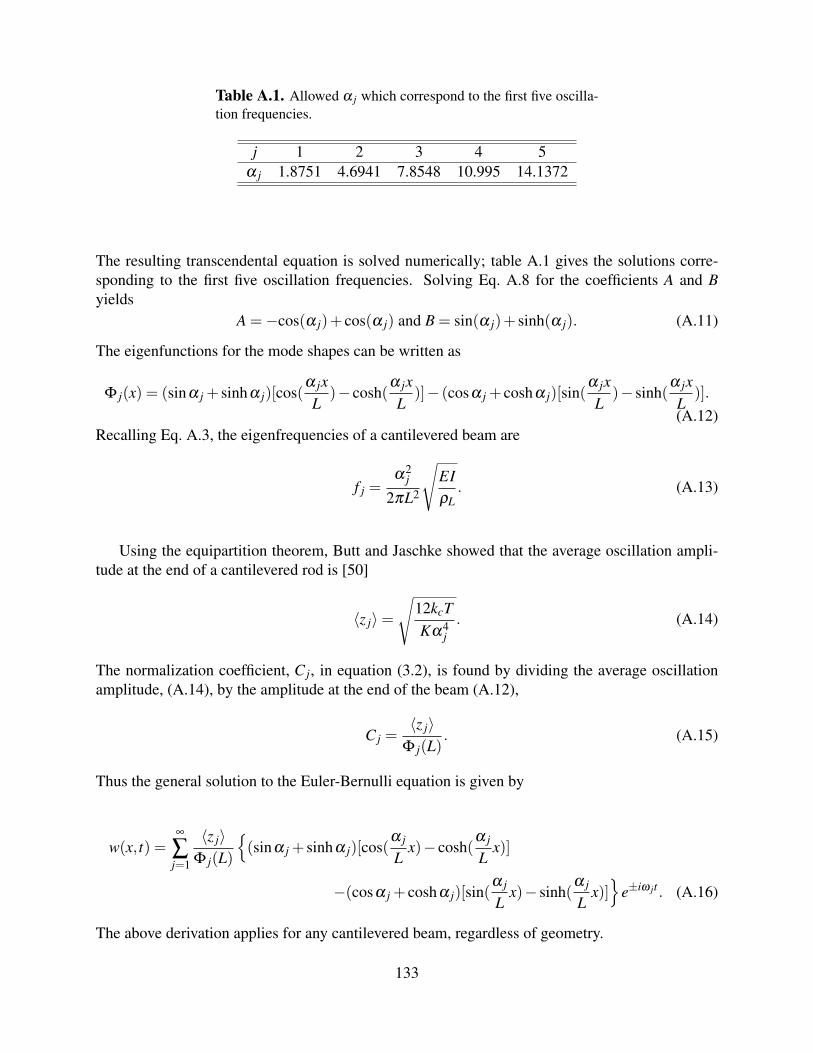
is solved numerically; Table 3.1 gives the solutions corresponding to the first five eigenfrequencies,f j. Appendix A gives a complete derivation of the eigenfrequencies and eigenmodes of oscillation.
The eigenfrequencies of oscillation for a cantilevered beam as a function of length are givenby [50]
f j =α2
j
2πL2
√EIρL
, (3.6)
assuming that I and ρ are constant along the length of the cantilevered beam.
In the case of a hollow cylinder, such as a MWNT, of inner diameter, di, and outer diameter,do, Eq. 3.6 can be rewritten as
f j =α2
j
8πL2
√Eρ
(d2o +d2
i ), (3.7)
where the substitutions I = π(d4o − d4
i )/64 and ρL = πρ(d2o − d2
i )/4 were used. For a solidnanowire (di = 0) Eq. 3.6 simplifies further to
f j =α2
j
8πL2 do
√Eρ
. (3.8)
For both MWNTs and Ag2Ga nanoneedles, typical lengths are 5–50 µm and outer diameters are50–200 nm. Based on TEM micrographs of MWNTs, di is estimated to be 0.5do. The density ofMWNTs is assumed to be that of graphite, 2300 kg/m3. From the stoichiometric ratio, ρ = 8960kg/m3 is estimated for Ag2Ga nanoneedles [48]. Estimates for the first eigenfrequencies rangefrom 10s of kHz for the longest nanowires to 1000s of kHz for short nanowires.
Table 3.1. Allowed α j which correspond to the first five oscilla-tion frequencies.
3.2 Frequency response function (FRF) for a cantilever
A cantilevered beam in a fluid (gas or liquid) is an example of a linear spring-mass system withviscous damping. In the time domain, the motion of such as system is described by Newton’s equa-tion of motion for damped, driven oscillations. The drive force, f (t), is assumed to be harmonic,but could represent many types of forcing, including acoustic, base, and thermal excitations. In thetime domain, the displacement z(t) of a linear spring-mass system is
mz+ cz+ kcz = f (t) (3.9)
where m is the mass of the cantilever, c is the damping, and kc is the static bending coefficient. Forthe case that f (t) is a harmonic forcing of the form Foeiωt , the solution to Eq. 3.9 is assumed to bez = Zei(ωt−δ ).
Since the eigenfrequencies of oscillation are of interest, Eq. 3.9 is converted to the frequencydomain by taking the Fourier transform of Eq. 3.9 which yields
−mω2Z(ω)+ icωZ(ω)+ kcZ(ω) = F(ω), (3.10)
where z(t)⇔ Z(ω) and f (t)⇔ F(ω). Solving Eq. 3.10 for Z(ω) yields the frequency responsefunction (FRF, also referred to as the linear response function), Z(ω)
Z(ω) =F(ω)
[−mω2 + icω + kc], (3.11)
where the transfer function is[−mω2 + icω + kc
]−1. Using the substitutions kc/m = ω2o and
c/m = ωo/Q [51], Eq. 3.11 can be re-written in terms of the resonant frequency ωo and qual-ity factor, Q, as
Z(ω) =F(ω)/kc[
1−(
ω
ωo
)2+ i ω
Qωo
] (3.12)
The magnitude of Z(ω) is
|Z(ω)|= F(ω)/kc√[1−(
ω
ωo
)2]2
+(
ω
Qωo
)2(3.13)
The above FRF is valid for any system described by Eq. 3.9, including cantilevered nanowires.Since the vibration spectra of the MWNTs were measured in the frequency domain, the eigen-frequencies f j and associated quality factors Q were found by fitting Eq. 3.13 to the measuredspectra.
The two frequency limits (ω ωo and ω ωo) suggest how a cantilevered nanowire canbe used as a vibrometer or accelerometer. To understand these limits, consider a sinusoidal base
35
motion of the form F(ω) = mω2Abase, where Abase is the base motion of the fixed end of thecantilever. In the low-frequency limit, Eq. 3.13 reduces to
|Z(ω)|= F(ω)kc
Abase, where ω ωo. (3.14)
Since |Z(ω)| is proportional to Abase, the cantilevered nanowire can be used as a vibrometer. In thehigh-frequency limit, Eq. 3.13 reduces to
|Z(ω)|= F(ω)mω2
o
(ωo
ω
)2=
accelerationω2 , where ω ωo. (3.15)
Thus in the high-frequency limit, the cantilever behaves as an accelerometer [52].
3.3 Power spectral density (PSD) of a cantilevered beam
With the Polytec MSA-400 system, measurements of the vibration spectrum in time can have amuch higher data resolution than those measured in frequency. For this reason, it is useful tomeasure the displacement (or velocity) of the thermally-excited cantilever in the time domain andFourier transform that signal to the frequency domain. This approach requires a statistically validmethod to transform the vibration spectrum into the frequency domain so that the eigenfrequencypeaks can be identified. Second, the appropriate theoretical response of the cantilever in the fre-quency domain must be derived.
3.3.1 Autocorrelation of a random signal
The Fourier transform of a signal is defined only for periodic signals. For this reason, it is notaccurate to directly take the Fourier transform of the time series measurement of a thermally-excited cantilever’s oscillation. Instead, the autocorrelation function, Rhh(τ), is first calculated.The autocorrelation function is a mathematical tool for finding periodic signals in random data andis defined as
Rhh(τ) = limT→∞
1T
∫ T/2
−T/2h(t)h(t + τ)dt (3.16)
where h(t) is a generic random signal in time, τ is a time interval, and T is the period. The double-subscript hh indicates the autocorrelation of h(t) with itself. The cross-correlation of signals g(t)and h(t) would be written as Rgh(τ). An important property of Rhh(τ) is that “If a random pro-cess has a periodic component, of period T, then the autocorrelation function also has a periodiccomponent of period T” (ref. [[53]], pg. 201). Taking the Fourier transform of Eq. 3.16 yields thepower spectral density (PSD) Shh(ω), which is defined as [53]
Shh(ω) =∫
∞
−∞
Rhh(τ)e−iωτdτ. (3.17)
36
For white noise, Shh(ω) is a constant.
For discrete data sets, the Fourier transform of the signal’s autocorrelation function can beaccomplished using the PWelch algorithm. This algorithm is implemented in Matlab following themethod of Welch [54]. For an example of the Matlab code used to analyze the time series data, seeAppendix E.
3.3.2 Power spectral density (PSD) of a cantilevered beam
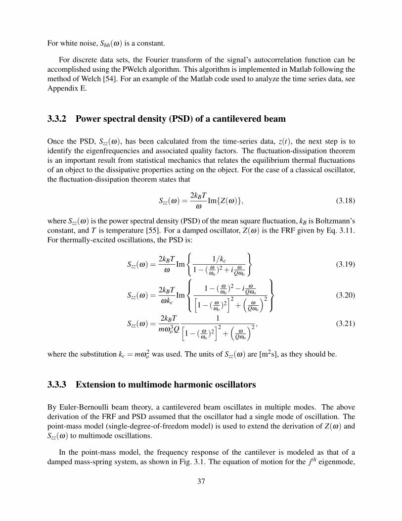
Once the PSD, Szz(ω), has been calculated from the time-series data, z(t), the next step is toidentify the eigenfrequencies and associated quality factors. The fluctuation-dissipation theoremis an important result from statistical mechanics that relates the equilibrium thermal fluctuationsof an object to the dissipative properties acting on the object. For the case of a classical oscillator,the fluctuation-dissipation theorem states that
Szz(ω) =2kBT
ωImZ(ω), (3.18)
where Szz(ω) is the power spectral density (PSD) of the mean square fluctuation, kB is Boltzmann’sconstant, and T is temperature [55]. For a damped oscillator, Z(ω) is the FRF given by Eq. 3.11.For thermally-excited oscillations, the PSD is:
Szz(ω) =2kBT
ωIm
1/kc
1− ( ω
ωo)2 + i ω
Qωo
(3.19)
Szz(ω) =2kBTωkc
Im
1− ( ω
ωo)2− i ω
Qωo[1− ( ω
ωo)2]2
+(
ω
Qωo
)2
(3.20)
Szz(ω) =2kBT
mω3o Q
1[1− ( ω
ωo)2]2
+(
ω
Qωo
)2 , (3.21)
where the substitution kc = mω2o was used. The units of Szz(ω) are [m2s], as they should be.
3.3.3 Extension to multimode harmonic oscillators
By Euler-Bernoulli beam theory, a cantilevered beam oscillates in multiple modes. The abovederivation of the FRF and PSD assumed that the oscillator had a single mode of oscillation. Thepoint-mass model (single-degree-of-freedom model) is used to extend the derivation of Z(ω) andSzz(ω) to multimode oscillations.
In the point-mass model, the frequency response of the cantilever is modeled as that of adamped mass-spring system, as shown in Fig. 3.1. The equation of motion for the jth eigenmode,
37
which has frequency ω j, is
M jeqz(t)+C j
eqz(t)+K jeqz(t) = f j(t), (3.22)
where z j(t) is the tip deflection of the jth eigenmode. The point-mass model of cantilever oscil-lations is valid for oscillations measured at the free end of the cantilever at frequencies near theeigenfrequencies. In this limit, the equivalent mass M j
eq, equivalent stiffness K jeq, and equivalent
damping C jeq must be identified.
Figure 3.1. A schematic of the the point-mass model for can-tilever oscillations assuming a stationary base.
The equivalent stiffness and equivalent mass, are defined as [56]
K jeq = kcα
4j /12 (3.23)
M jeq = m/4. (3.24)
The stiffness of the cantilever increases dramatically for higher eigenmodes (eg: K j=1eq /kc =1.03,
K j=2eq /kc=40.5, K j=3
eq /kc=317), while the equivalent mass is independent of eigenmode [56]. Thedamping is unchanged for higher eigenmodes; C j
eq = c.
Substitution of K jeq, Q j, M j
eq into Eq. 3.12 for the FRF and Eq. 3.19 leads to
Z(ω) =F(ω)/K j
eq[1−(
ω
ω j
)2+ i ω
Q jω j
] (3.25)
and
Szz(ω) =N
∑j=1
2kBT
M jeqω3
j Q j
Φ2j(x)[
1− ( ω
ω j)2]2
+(
ω
Q jω j
)2 . (3.26)
where Φ j(x) is the cantilever deformation of the jth eigenmode, as defined previously [57].
38
3.4 Damping and quality factor of cantilevers in fluids
The quality factor Q of an oscillation is proportional to the ration of the energy stored to thatdissipated, that is
Q = 2πEstored
Ediss. (3.27)
For a linear harmonic oscillator, Eq. 3.27 can be expressed as [58]
Q =kc +mω2
2cω; at resonance, Q =
mωo
c. (3.28)
Assuming an ideally cantilevered nanowire (ie: displacement and velocity at the fixed end arezero), mechanisms for the damping of the nanowire’s vibrations include cs, the structural dampingdue to phonon modes and defects in the nanowire, and c f , the damping due to the ambient fluid(gas or liquid). The total damping is c = cs + c f . The fluid damping depends primarily on thediameter of the nanowire and the pressure of the surrounding fluid.
In order to calculate reasonable estimates for Q, c must be known. For fluid damping of nanos-tructures, c f cs, so cs can be neglected. For all the experiments in this report, the surroundingfluid is standard lab atmosphere, at pressures, P, of 760 Torr and lower. In this gaseous environ-ment, three different fluid flow regimes can be applicable for the calculation of c f , depending on Pand the dimensions of the nanowire or Si microcantilever.
3.4.1 Damping in the continuum, cross-over and free-molecular regimes
The effect of fluid damping c f depends on the dimensions of the cantilever (eg: nano-wire or Simicrocantilever) and the density of the surrounding fluid. The Knudsen number, Kn, is a dimen-sionless parameter that can be used to characterize fluid flow regimes:
Kn = lm f p/wrep, (3.29)
where lm f p is the mean free path of the gas molecules, 65 nm for air at STP, and wrep is a rep-resentative length scale, the width, w, or diameter, do, of an oscillating cantilever [58]. The flowregimes are defined as continuum (Kn ≤ 0.01), cross-over (0.01 < Kn ≤10), and free molecularregime (Kn > 10). In the continuum regime, air pressure, P, is considerable and viscous forces acton the cantilever. In the cross-over regime, the air molecules interact slightly with the cantilever.At the low relative pressures of the free molecular regime, the forcing is due solely to momentumexchange of the molecules striking the cantilever and the air-cantilever interactions are describedusing statistical mechanics [59]. Since the damping c f depends on the flow regime, it is importantto identify the appropriate flow regime.
During the course of this work, the vibration spectra of numerous nanowires and a few stan-dard Si microcantilevers, including the µmasch NSC35, were studied. Diameters of 75 nm and
39
150 nm are representative of the MWNTs and Ag2Ga nanoneedles studied; the width of theµmasch NSC35 microcantilever is w = 35 µm.
Using these parameters, the Knudsen number is calculated as a function of pressure between10 mTorr and 1000 Torr (Fig 3.2). The damping of the Si microcantilever spans all three flowregimes in the pressure range plotted, while at atmospheric pressures and below, damping ofthe nanowire is in the cross-over and free molecular regimes. The cut-off pressure between thecross-over and free molecular regime is 35 Torr and 75 Torr for the 75-nm and 150-nm diame-ter nanowires, respectively. At atmospheric pressure, silicon microcantilevers are in the viscouscontinuum regime while nanowires are in the cross-over regime.
Figure 3.2. Knudsen numbers calculated for the 35-µm widecantilever and two nanowires of different diameters. Shaded re-gions indicate the free molecular flow, cross-over, and continuumregimes. The dashed vertical line indicates 760 Torr.
Fluid damping coefficient
The fluid damping coefficient, c f , is a function of pressure and is given by different expressionsin the continuum, crossover, and free molecular regimes. All three expressions for c f contain acommon term equal to ρ f Uth, where ρ f is the gas density and Uth is the rms air speed, Uth =√
3kbNATMm
[58]. In Uth, NA is Avogado’s constant and Mm is the molecular weight of the gas (eg.29.87 g/mol for Earth’s atmosphere) [60]. Using the ideal gas law, the fluid density ρ f can be
40
expressed in terms of the gas temperature T and pressure,
PV = nRoT → P =mgas
VRoTMm→ ρ f = P
Mm
RoT, (3.30)
where the universal gas constant is Ro = NAkB = 8.314 J/(mol K) and mgas is the mass of the gas.Thus the aforementioned common term can be expressed as
ρ f Uth = P
√3Mm
RoT(3.31)
which appears in the below expressions for c f . These definitions for c f in the continuum, cross-over, and free molecular regime are from Ref. [58].
c f =√
3[1.41βKcKn]Lwrep P
√Mm
RoTKn≤ 0.01, continuum regime (3.32)
c f = 2√
3π3/2Kn
αKnLwrep P
√Mm
RoT0.01≤ Kn≤ 10 cross-over regime (3.33)
c f =Fd
u= 2√
3Lwrep P
√Mm
RoTKn > 10, free molecular regime. (3.34)
Continuum c f : The continuum fluid damping coefficient depends on the cantilever’s dimen-sions (L and wrep), the gas properties, and dimensionless parameters β and Kc. Kc, a fluiddensity parameter, is a function of β and is given in Ref. [58]. The dimensionless param-eter β = Re/(4Pw) is a function of the Reynolds number, Re, and a frequency parameterPw = Acant/wrep, where Acant is the oscillation amplitude of the cantilever. The Reynoldsnumber is Re = ρ f Ucant wrep/µ where µ is the dynamic viscosity of the fluid (gas) andU = Acantω is the oscillation velocity of the cantilever [58].
Cross-over c f : The cross-over fluid damping coefficient is proportional to the free molecular fluiddamping coefficient and depends on the Mach number, Knudsen number, and dimensionlessparameter αKn, where
αKn = ln(
2√
πKnS
)− γ +0.5+Λ
√πKn. (3.35)
The Mach number is S = Ucant/Usound; γ is the Euler constant, 0.5772; and Λ, which variesbetween 1 and 1.5 in the cross-over regime, is given by
Λ = 1+12(1− e−Kn/2). (3.36)
Free molecular c f : The free molecular fluid damping coefficient is independent of Knudsennumber and depends linearly on the cantilever dimensions and pressure. The free molecularfluid damping is proportional to the drag force Fd and a velocity term u.
The non-dimensionalized fluid damping coefficients, c f /(πµL), are plotted in Fig. 3.3 for theSi microcantilever and two nanowires. As defined previously, L is the length of the cantilever ornanowire and µ is the dynamic viscosity, µ = 0.45
√3lm f pP/
√RoT [58].
41
Figure 3.3. The non-dimensionalized fluid damping coefficientsare plotted for the three cantilevers for the case of free molecular(·), cross-over (o), and continuum (+) flow regimes. The cross-over solution underestimates the cross-over damping, resulting ina discontinuity between the cross-over (0) and continuum flow (+)regimes.
3.4.2 Calculated quality factor due to gas damping at atmospheric pressure
Following Eq. 3.28, the quality factor of the jth eigenmode is
Q j =mω j
c f + cs; (3.37)
when c f cs, Q j is inversely proportional to c f .
Equation 3.37 and the expression for c f in the cross-over regime are used to calculate Q at760 Torr for nanowires of L = 10 µm, do = 100–200 nm. For MWNTs of these dimensions, Q1= 3–18; for Ag2Ga nanoneedles of these dimensions, Q1 = 10–60. The above expressions for c fand Eq. 3.37 are used in the calculation of the minimum detectable mass for cantilevered nanowiresensors (section 5.5).
42
Chapter 4
Experimental details for measurements ofthe vibrational spectra of nanowires
4.1 Polytec MSA-400 scanning vibrometer
Nanowire oscillations were recorded using a Polytec MSA-400 scanning LDV. To reduce noisefrom flood vibrations, the LDV is situated directly on top of a 30,000 kg cement slab supported bysix air spring dampers. The vibrometer consists of a modified Mach-Zehnder interferometer withan optical microscope in the signal leg of the vibrometer. The object beam of the interferometer(wavelength λ=633 nm, power <1 mW) is focused through a microscope objective and is incidentnormal to the vibrating nanowire. As shown in Fig. 4.1(a), the backscattered beam is recombinedwith a reference beam to form an interference signal which is decoded and Fourier transformedto yield the vibrational spectra of interest. The LDV can measure velocities in the spectral rangefrom 0–1.5 MHz and displacements in the spectral range from 50 kHz–20 MHz. The frequencyresolution is 100 Hz for a typical 0-10 MHz frequency scan, allowing for a high resolution ofspectral features.
In the case of the displacement spectra measurements, the backscattered beam is phase-shifteddue to the change in the position of the nanowire as it vibrates. When the phase-shifted backscat-tered beam is recombined with the reference beam, the resulting interference pattern is decodedusing a fringe-counting method. The velocity spectra measurements were decoded using the well-known Doppler effect. The nanowire’s oscillatory motion with amplitude A and velocity v atfrequency f caused the backscattered light, which the LDV collects, to be Doppler shifted by afrequency
∆(t) = ν′−ν =−v
cν cos(2π f t), (4.1)
where v = A(2π f ) and ν = c/λ , where c is the speed of light. When the Doppler frequency shiftis measured at an eigenmode of the MWNT, ∆(t) is proportional to the resonant frequency f j andamplitude A j of the jth eigenmode. Numerous tests of the LDV show that the frequencies aremeasured with high accuracy.
However, the measured amplitude of the LDV is only proportional to the actual displacementor velocity. When most of the reflected beam is collected by the sensor, the error between the mea-sured and actual amplitude is small (<10 percent). If only a small percentage of the reflected beam
43
Figure 4.1. In (a), a schematic of the Polytec LDV used in thiswork, following Ref. [14]. The circularly polarized laser beam issplit by a beamsplitter into an object and reference beam. The ob-ject beam is focused through a 50× objective onto the vibratingnanostructure, usually a nanowire. This backscatted object beamis then recombined with the reference beam, whose frequency hasbeen shifted by νBragg = 40 MHz. In (b), a schematic diagram ofa cantilevered nanowire. The reflected light (R) of the normallyincident laser beam (I) is Doppler shifted by frequency ∆ whenreflected from the MWNT. In (c), an illustration of the relativedimensions when the object beam is focused through the 50× ob-jective. As indicated by the shaded region, the beam waist is muchwider than the nanowire.
is collected by the sensor (small signal return), then the measured signal is only proportional tothe local displacement or velocity of the nanowire and a quantitative estimate of the local velocityor amplitude becomes problematic, even though the frequencies are accurately measured. Smallsignal returns occur (a) when the LDV laser spot lies on the edge of a vibrating structure or (b)when the vibrating object is much smaller than the spot size of the beam.
Figure 4.2(b) shows the measured operating deflection shape (ODS) of the first eigenmode ofvibration of an Ag2Ga nanoneedle, which was measured at 13 points along the nanoneedle. Themeasured ODS corresponds well to the theoretical first eigenmode of vibration for all but the tip-most data point. The displacement of this tip-most data point is only 75 percent of the expectedvalue, which was normalized to unity. The under-measurement of the displacement indicates thatthe LDV laser spot likely lay on the very end of the nanoneedle, as indicated by the red circle
44
Figure 4.2. In (a), an SEM of the 16.6 µm long, 140 nm diameternanoneedle NNB2. Two red circles, diameter 0.9 µm, indicate thespot size of the laser. In (b), the measured ODS and theoreticalfirst eigenmode, both normalized. The laser return at the tip-mostpoint on the nanoneedle was poor; for this reason the last data pointunder-estimates the displacement amplitude.
drawn on the tip of NNB2 in Fig. 4.2(a).
Since the MWNTs were relatively poor light scatters, all MWNT displacement and velocityspectra were normalized to a maximum value of unity. Spectra from Ag2Ga nanoneedles and Sicantilevers are presented with the measured amplitude reported by the LDV, which may differ fromthe actual amplitude.
4.2 Calibration of LDV by measuring the thermal tuning curveof a Si microcantilever
As mentioned above, the LDV output is proportional to the local displacement or velocity. Tocheck that that measured amplitude of the LDV is reasonably accurate, the thermal spectra of aconventional silicon microcantilever was measured. By the equipartition theorem (section 4.2.1),the thermal energy is equally divided between the potential energy and kinetic energy. The poten-tial energy, Epotential is proportional to the spring constant of the cantilever, kc, and mean squaredisplacement, 〈z2〉.
12
kBT =12
kLDV 〈z2〉= 12
kAFM〈z2〉, (4.2)
45
where kLDV and kAFM are kc estimated from Sader’s method using the LDV and AFM spectrarespectively. Sader’s method (section 4.2.2) gives a method of measuring kc from the qualityfactor and frequency of the resonant peak of a cantilever oscillating in a fluid of known density anddamping. If the LDV calibration is accurate, then the measured Epotential should equal Ethermal ,assuming the cantilever is in thermal equilibrium with the surrounding atmosphere.
The vibration spectrum of a silicon AFM cantilever was measured using both the LDV and theNanotec Electronica AFM. For both measurements, kc was estimated from the vibration spectrausing Sader’s method. Using these kc and the mean 〈z2〉 measured by the LDV, Epotential wascalculated and compared to Ethermal . The experimental details of these measurements are given insection 4.2.1; the calculated energies are given in Table 4.1.
4.2.1 Experimental details
Asylum Si3N4 microcantilever: An Asylum Research RC800 PSA silicon nitride microcantileverwas studied. The manufacturer dimensions are L = 100 µm and w = 20 µm with a nominal kc =0.39 N/m. These dimensions were confirmed by measurements with the LDV’s 50× optical micro-scope. This cantilever was chosen since it had a small nominal spring constant and a rectangularcross-section.
Nanotec AFM: The cantilever was mounted in the Nanotec chip holder and its tuning curvewas measured using the Nanotec Electronica AFM. The drive voltage for this measurement was0.02 V. The measured tuning curve and the associated curve fit for the frequency response function(FRF) are plotted in Fig. 4.3(a).
Polytec LDV: The cantilever, still in the Nanotec chip holder, was then mounted in the fieldof view of the LDV. The Nanotec chip holder, held securely in the jaws of an alligator clip, waspositioned using an XYZ micromanipulator. This arrangement allowed the LDV’s signal beam tobe focused on the flat side of the cantilever. For these calibration tests, the laser spot of the LDVwas focused fully on the end of the cantilever. Since the signal return was maximum, the measuredamplitude was as accurate as possible using the LDV.
The displacement as a function of time, zmeas(t), was measured at the free end of the cantilever.The displacement was measured at 1,048,576 time points over 4.096 sec, resulting in a time resolu-tion of ∆t = 3.9 µs. By the Nyquist criterion, 2 fNyquist = 1/∆t, the minimum measurable frequencyfNyquist was 128 kHz.
Using the PWelch algorithm detailed in Appendix E, the power spectral density (PSD) of thedisplacement zmeas(t) was calculated. This PSD is plotted in Fig. 4.3(b); averaging over 64 fre-quency windows smoothes the data. To determine Q and f1, the following curve fit,
Szz( f ) =A
Q1 f 31
1[1− ( f
f1)2]2
+(
fQ1 f1
)2 +Noise, (4.3)
which is of the form of Eq. 3.19, was fit to the PSD (64 windows) using Matlab’s curve fitting
46
toolbox (cftool). In Eq. 4.3, the term A includes the parameters of temperature and cantilevermass; Noise is a small constant offset.
Figure 4.3. (a) The FRF of a Si3N4 cantilever, as measured usingthe Nanotec AFM. (b) The power spectral density measured usingthe LDV for the same Si3N4 cantilever. This figure shows the ef-fect of averaging the PSD over 4 (green) and 64 (blue) windows.A curve fit (black) is fit to the 64-window data.
4.2.2 kc from Sader’s method for AFM and LDV data
Sader’s method is regularly used to calibrate the static bending stiffness kc of AFM cantileversand is implemented in a Nanotec AFM. Assuming a rectangular cantilever of width w, the staticbending coefficient kc is then
kc = 0.1906ρ f w2LQ f Γi(ωo)ω2o , (4.4)
where ρ f is the density of the surrounding fluid, Q f is the quality factor of the cantilever’s os-cillation in fluid, Γi is the imaginary part of the hydrodynamic damping function, and ωo is thefundamental resonant frequency, also measured in fluid [61].
Ryan Wagner measured the tuning frequency response function (FRF) [Fig. 4.3(a)] using theNanotec Electronica AFM. From a curve fit to the FRF (Eq. 3.13), we determined f1 = 69.81 kHzand Q = 89. Using Sader’s method and the measured quantities and cantilever dimensions givenabove, we calculated kc = 0.32 N/m.
For the LDV data, Q = 86 was determined by the curve fit of Eq. 4.3 to the PSD, which wascalculated using 64 windows. From this Q, kc = 0.31 N/m was calculated using Sader’s method.Thus the calculated kc from the AFM tuning curve and the LDV PSD are in good agreement.
47
4.2.3 Calculation of 〈z2〉 from zmeas(t) and from the PSD
From the LDV measurement, the mean square displacement 〈z2〉 of the cantilever can be calculatedeither directly from zmeas(t) or indirectly from the PSD. By Parseval’s theorem, the total energy ofa signal in the time and frequency domain are equal; that is,
∫∞
−∞
dt h2(t) =∫
∞
−∞
d f |H( f )|2, (4.5)
where h(t) and H( f ) are a Fourier transform pair [62].
The deflection at the tip of the cantilever, zmeas(t) was measured using the displacement de-coder of the LDV. After correcting for the offset, the mean deflection in the time domain 〈z2
time〉=0.0105× 10⁻¹⁸ m2 was calculated. This calculation assumes that the deflection of the cantileverat its tip is due solely to the motion of the first eigenmode, z1. While zmeas > z1, the mean squaredeflection of the first eigenmode is 39 times that of the second (〈z2
1〉/〈z22〉 = α4
2/α41 = 6.274), so
the assumption that 〈z2time〉 ≡ 〈z2
1〉 is accurate to 2 percent.
A better measure of the energy in a single eigenmode is calculated by integrating the PSD.From Eq. 4.5, ∑
all modes〈z2
f req, j〉, the mean square deflection in the frequency domain, should equal
〈z2time〉. From the PSD, 〈z2
f req, j〉 is calculated by numerically integrating (trapezoidal integration)the PSD over the width of the eigenmode. 〈z2
f req,1〉= 0.0094 nm2 was calculated by integrating thePSD over a frequency range of 5 kHz, which was centered at f1 = 69.81 kHz. The value of 〈z2
f req,1〉should be more accurate than the value of 〈z2
time〉 because 〈z2f req,1〉 only contains contributions from
the first eigenmode.
4.2.4 Comparison of the potential and thermal energy of a Si3N4 cantileverin thermal equilibrium
Following Eq. 4.2, the potential energy can now be calculated as 12kc〈z2〉, where kc is determined
by AFM or LDV. Assuming a room temperature of 293 K, Ethermal is given by (1/2)kBT , which isequal to 2.02×10⁻²¹ J.
The calculated Epotential , as calculated using kc measured from the AFM and LDV, are givenin table 4.1. The error in the measurement is defined as (Ethermal−Epotential/Ethermal). The errorof the measured Epotential is 25 percent, which suggests that the measured 〈z2〉 is ∼25 percent toosmall. The measured Si3N4 cantilever is an uncoated cantilever and likely has poor reflectivity.
48
Table 4.1. Potential energy of a Si3N4 cantilever, using 〈z2f req〉
= 0.0094 nm2 and K1eq = α4
1 kc/12. The Q is determined from thecurve fit to either the AFM or LDV data.
Method Q K1eq (N/m) Epotential×10−21 J % Error
AFM 89 0.33 1.6 23LDV 86 0.32 1.5 26
4.3 The MWNT-Ni STM tips
The MWNTs used in this experiment were grown at 900 oC in a SEKI AX5200S microwavePECVD reactor using Fe2O3 nanoparticle catalyst particles [63]. These MWNTs were grown byDr. Placidus Amama of Prof. Tim Fisher’s research group at Purdue University. Chun Lan of theReifenberger Nanophysics Lab had studied the electronic properties of PECVD-grown MWNTsas a function of growth conditions. She discovered that MWNTs grown at 900C had a lowerresistance and, thus fewer defect sites, than MWNTs grown at 800C or 900C [64].
4.3.1 Literature review of affixing MWNTs to AFM tips
The techniques used for affixing MWNTs to STM tips strongly follow the procedure used for cre-ating MWNT-AFM probes. In 1996 Dai et al. reported affixing MWNTs to both silicon cantileversand STM tips using an acrylic adhesive and van der Waals force. Although they reported atomicresolution STM scans of TaS2 using a∼5-nm wide MWNT protruding from a MWNT bundle [65],future work from this group and others focused on MWNT-AFM probes.
Researchers at NASA Ames Research Center realized the potential of Ni-coated cantileversfor fabricating MWNT-tipped AFM probes and developed a technique for transferring a singleMWNT to a probe tip using micromanipulators [66]. Using carbon vapor deposition (CVD), acartridge of MWNTs was grown on a PtIr wire in preparation for the MWNTs’ transfer to siliconcantilevers coated with∼10–15 nm of nickel. The MWNT cartridge and Ni-coated cantilever, heldby micromanipulators, were brought into close proximity under an optical microscope. When asolitary MWNT suitable for transfer was found, a small electric field (3–10 V) was applied betweenthe cartridge (anode) and cantilever (cathode) to induce the MWNT to contact the cantilever. Thenthe voltage was increased to 10–40 V causing the MWNT to break from the cartridge and weld tothe Ni-coated cantilever by current-induced joule heating [66, 67]. These MWNT-AFM probes areextremely stable; no degradation in AFM scan quality was seen after scanning continuously for15 hours [68].
49
4.3.2 Creating MWNT-Ni STM tips
Etching Ni tips
The nickel wires were etched into high-aspect ratio STM tips using an electrochemical tip fabrica-tor, Schrodinger’s Sharpener (Model SS02, manufacturer Obbligato Objectives). The Schrodinger’sSharpener consists of a clamp to hold the wire being etched, a dual platinum ring assembly whichsupports the etching laminar, and a detection system with an electronic current break. The nickelwire, held vertically by the anode clamp, extends through the dual ring assembly. Etching occursin the top ring (cathode) of the coaxial dual ring assembly. The detection system monitors currentthrough the bottom sense ring, cutting off the current and stopping the etch as soon as the wire isetched through.
A nickel wire is cut to a length of 5–6 cm and clamped in the Schrodinger’s Sharpener. Thenthe dual ring assembly and wire are dipped in the etchant, a 2M solution of KCl dissolved in Birckultra-pure water. Often the rings and wire must be dipped a few times before a stable laminar filmforms on both rings. Next a small ball of Play-Doh (∼5 mm diameter) is slid on the free end ofthe nickel wire. The extra weight of the Play-Doh helps ensure that the tips from both the top andbottom halves of the wire are sharp, avoid torque at the tip etch point, and stop corrosion of thelower tip by causing it to fall as soon as etching is complete [69]. An added benefit is that thePlay-Doh ball protects the lower tip as it falls, decreasing the probability that the lower tip willbe bent on impact. The Schrodinger’s Sharpener control electronics apply a 2.0 VDC voltage andetching begins with the following chemical reaction [69],
Cathode: 2H2O + 2e− → H2(g) + 2OH−
Anode: Ni(s)+4Cl− → NiCl24 + 2e−.
As the etching proceeds, green NiCl24 salts accumulate along the Pt ring. Occasionally the laminarin either ring breaks before the etching is completed. In that case the Play-Doh ball is removed, therings and wire are again dipped in etchant, the Play-Doh ball is replaced, and the etching voltageapplied again. To etch a good pair of Ni-STM tips typically required 5–10 minutes. After etchingis complete, the tips are held in an ultrasonic bath of Birck ultra-pure water for a minute to removesalts and then rinsed with isopropanol to remove oils.
Affixing MWNTs to Ni-STM tips
Individual MWNTs were affixed to etched nickel STM tips using the procedure described byStevens et al. [66]. This procedure was observed under a darkfield microscope (Zeiss JenoptikD-07739), which has 5x and 50x magnification. A pair of XYZ nanomanipulators hold the Ni-STM tip and the MWNT cartridge above the microscope stage. To prepare the MWNT cartridge,a small (∼ 3× 3 mm) piece of conducting SEM tape is held in a alligator clip so that it barelyprotrudes past the end of the clamp. The SEM tape is then dipped in a sample of matted MWNTs.The mats of MWNTs are gently brushed off, leaving MWNTs stuck in the SEM tape at randomdirections.
50
To make the MWNT attachment more robust, the Ni tip is touched to soft double-sided carbonscanning electron microscope (SEM) tape (STR tape from Shinto Paint Co. Ltd.) before addingthe MWNT. A small amount of adhesive from the SEM tape sticks to the Ni tip and helps affix theMWNT. Without the adhesive from the SEM tape, the forces of adding a glass bead to the MWNTwould frequently push the MWNT off the Ni tip.
Under the 5x magnification, the MWNT cartridge and Ni-STM tip are brought a few hundredmicrons of each other. The magnification is increased to 50x and MWNT cartridge is scanned tofind a solitary MWNT sticking out roughly perpendicular to the cartridge. The desired MWNT isbrought into focus and the Ni-STM tip is brought within close proximity using the nanomanipu-lators. The shallow focal plane of the darkfield microscope ensures that if both the MWNT andNi-STM tip are in focus, they must be in the same plane. The Ni-STM tip is then brought alongsidethe MWNT with 5–10 µms of overlap. At this point van der Waals attraction causes the MWNTto snap in contact with the Ni-STM tip. The Ni-STM tip position is adjusted slightly, if necessary,so that the MWNT contacts the Ni-STM tip along the tip’s length and not just at one point. An HP6234A Dual Power Supply, applies a 10–30 V voltage pulse to the MWNT (anode) and Ni-STMtip (cathode). This voltage pulse breaks the MWNT off of the SEM tape and firmly bonds theMWNT to the Ni-STM tip. Figure 4.4 is a darkfield image of a typical MWNT-Ni STM tip.
Figure 4.4. Darkfield image of a 13.5 µm MWNT affixed to anickel STM tip. The magnification is 50x.
4.4 Ultimate measurement limits for LDV calculated using Miescatting theory
When a cylinder (such as a nanowire) is illuminated by light, the amount of light scattered andabsorbed depends in a complicated way on the geometry and optical properties of the cylinder,the index of refraction of the surrounding medium, and the wavelength and polarization of the
51
incident light beam. When the incident wavelength becomes comparable to the dimensions ofthe cylinder, Mie scattering theory rather than geometrical optics is applicable. In Mie theory,the scattering cross section per unit length of the cylinder, Csca, depends on the diameter of thecylinder do, the complex index of refraction of both the cylinder (N) and surrounding medium(Nmed), and the wavelength (λ ) and angle of incidence of the light beam. From these parameters,expressions for Csca far from the cylinder can be derived [70]. A particularly useful quantity isthe scattering efficiency Qsca, which is defined as Qsca = Csca/do. If Qsca is greater than 1, thenlight is effectively scattered from an apparent object that is larger in cross-section than the actualscattering object.
Following Bohren and Huffman [70], Qsca is calculated for the case of light (of wavenumberk) normally incident on a cylinder,
QT Msca = 2
χ(|bo|2 +2∑
∞n |bn|2)
QT Esca = 2
χ(|ao|2 +2∑
∞n |an|2),
(4.6)
where the dimensionless size parameter, χ , equals ka [70]. In the case of circularly polarized light,the transverse magnetic (TM) and electric (TE) modes contribute equally, so Qsca = 1
2(Qsca,T M +Qsca,T E) [71]. The coefficients a and b are a function of the ratio of the index of refraction of thesurrounding medium (Nmed) to that of the cylinder (Ncyl) and the size parameter x.
an = ηJ′n(χ)Jn(ηx)−Jn(χ)J
′n(ηx)
mJn(ηχ)H(1)′n (χ)−J′n(ηχ)H(1)
n (χ)
bn = Jn(ηχ)J′n(χ)−ηJ
′n(ηχ)Jn(χ)
Jn(ηχ)H(1)′n −ηJ′n(ηχ)H(1)
n (χ), where n = 0,1,2, ...
(4.7)
where H1n is a Hankel function (H1
n = Jn + iYn), Jn and Yn respectively are Bessel functions of thefirst and second kind, and η = |Ncyl|/|Nmed|.
We use Mie theory to calculate the scattering efficiency Qsca of graphite, silver, and siliconnanowires, which are modeled as dielectric cylinders of diameter do. This calculation allows usto better understand the limits of light scattering from a nanowire and to estimate the smallestdiameter nanowire whose oscillation might be detected. A FORTRAN program for calculatingQsca as a function of incident angle was modified to calculate Qsca as function of do, N, andNmed [70]. This modified FORTRAN program and a sample output are given in Appendix D.Calculations of Qsca are plotted in Fig. 4.5 and were performed for the case of circularly polarized633-nm light to match the conditions of our experiments.
Optical constants for MWNTs and Ag2Ga nanoneedles are not well established. However,a MWNT is similar in structure to pyrolitic graphite for which the optical constants are known.With this in mind, any light reflected from the front surface of a MWNT scatters from graphiticplanes similar in orientation to the [0001] basal plane of graphite. Any light scattered from theouter edge of a MWNT reflects from graphitic planes similar in orientation to the [1120] plane ofgraphite. Following this logic, realistic limits on Qsca can be obtained using the appropriate opticalconstants of pyrolytic graphite [72]. The index of refraction for silver (NAg = 0.135+ i3.99) is usedas a rough approximation for the N of Ag2Ga nanoneedles [73].
52
Figure 4.5. The calculated Qsca for circularly polarized 633 nmlight normally incident on a cylindrical nanowire in air as afunction of diameter. In (a), the case of light scattering off ofmetallic silver (NAg = 0.135 + i3.99; solid red line) and graphiticnanowires. For the graphitic nanowires, light scattering off the[0001] plane (NG = 1.5+ i0; dotted cyan line) and the [1120] plane(NG = 2.7 + i1.4; solid blue line) are considered. The diametersof MWNTs studied fall within the range indicated by the dashedvertical lines. In (b), the case of light scattering off of a semicon-ducting silicon nanowire (NSi = 3.877+ i0.019).
We conclude from Fig. 4.5(a) that for diameters less than ∼250 nm, the edges of the MWNTwill more effectively scatter light. Assuming that the signal-to-noise ratio (SNR) of the vibrationalresonance peak is proportional to the amount of light scattered, we can estimate the smallest diam-eter MWNT that reflects just enough light so that its oscillation might be detected. From our mea-sured data, we typically find a SNR at resonance of 5:1. We define the smallest diameter MWNTwhose oscillation spectra can be measured as a MWNT that scatters light at resonance with a SNRof 1:1. From the calculations leading to Fig. 4.5(a), we estimate that MWNTs with diameters be-tween 70 and 100 nm meet the SNR criterion of 1:1. This suggests that MWNTs with diameters inthe range between 70 and 100 nm are the smallest diameter MWNTs that can be studied using thePolytec MSA-400 scanning LDV. To date, the smallest diameter Ag2Ga nanoneedle studied hada diameter of 60 nm. This nanoneedle still reflected sufficient light so that its oscillation spectracould be recorded.
Since Qsca depends strongly on the index of refraction N of the cylinder, nanowires of othermaterials might scatter light more effectively, thereby allowing the vibrational spectra of smallerdiameter nanowires to be detected. Consider the case of Si(111) nanowires which have N = 3.9+i0.02 [74]. Calculations give a Qsca one to two orders of magnitude higher than MWNTs of thesame diameter, suggesting that the oscillation of silicon nanowires can be measured to diametersless than 50 nm [Fig. 4.5(b)].
53
54
Chapter 5
Measured vibration spectra, elasticmodulus, and quality factors of MWNTsand Ag2Ga nanoneedles
5.1 Qualitative MWNT vibration spectra
Our first experiments to measure the vibration spectra of MWNTs were low-resolution qualitativemeasurements to estimate the resonant frequency of individual MWNTs. 1 A priori we had as-sumed that the elastic modulus of the PECVD-grown MWNTs was∼1 TPa, as it is for SWNTs andpristine arc-discharge MWNTs. Using E=1 TPa and approximate MWNT dimensions of 5-10 µm,do = 100 nm, and di = 0.5do, the resonant frequency was estimated to be in the 10s of MHz.
To obtain rough estimates for f1, we electostatically excited MWNTs affixed to nickel STM tipsand observed the oscillation in a darkfield microscope. The design of the electrostatic excitationexperiment was inspired by the work of J. Galliard et al. [34] and by conversations with Dr. SteveHowell of Sandia National Laboratories. Both the MWNT, mounted on a Ni STM tip, and anetched Ni STM tip counter electrode were held in alligator clips. Using nanomanipulators, theMWNT and counter electrode were positioned nearly perpendicular to each other, approximately2–4 µm apart, as shown in Fig 5.1(a). This perpendicular configuration was chosen to maximizethe electric field on the MWNT. Care was taken to ensure that the gap distance was large enoughto prevent the MWNT from snapping into contact with the MWNT; such contact would cause theMWNT to spark shorten.
The MWNT tip was biased by 30 VDC to draw charge to the tip of the MWNT. A DC biasapplied between the MWNT and electrode caused the MWNT to bend toward the Ni electrode.If the point of attachment were weak, the MWNT would pivot at MWNT-Ni tip junction. As theelectrostatic drive frequency was increased, the magnitude of the oscillation was monitored in thedarkfield microscope. At low excitation frequencies (∼2-20 Hz), the MWNT would oscillate withamplitude 1–2 µm. As the drive frequency was increased past∼50 Hz, the amplitude of oscillationdecreased to near zero. The frequency response remained flat until the drive frequency approached
1Portions of this chapter were previously published in Ref. [75], L. B. Biedermann, R. C. Tung, A. Raman, andR. G. Reifenberger, “Flexural vibration spectra of carbon nanotubes measured using laser Doppler vibrometry,” Nan-otechnology 20:3 035702 (2009). Please see the copyright statement in Appendix F.
55
Figure 5.1. In (a), a schematic of the experimental set-up forelectrostatic excitation of a MWNT. In (b), the electrostatic excita-tion of MWNT A7a−9 at resonance. The E for this MWNT wascalculated to be 4.1 GPa.
the resonant frequency. At resonance, the approximate vibration amplitude was 1–2 µm with adrive voltage of 20 Vpp, as shown in Fig. 5.1(b).
The oscillation amplitude depends strongly on the distance between the MWNT and the counter-electrode to which the AC electric potential was applied. Decreasing the MWNT-electrode distanceincreased both the oscillation amplitude and the risk of the MWNT contacting the electrode andspark shortening. We noted the resonant frequency by an increase in the oscillation amplitude, butthe resolution of our frequency measurements was low, ∼50 kHz.
Figure 5.2 shows the calculated E for seven MWNTs whose resonant frequencies were esti-mated using electrostatic excitation. By inverting Eq. 3.7, E is written as
E =(8π)2ρ
α4j (d2
o +d2i )
f 2j L4. (5.1)
For these calculations of E, do was assumed to be 180 nm and di = 0.5do. Two MWNTs, A7a−2and A7b− 2, had exceptionally low moduli of 0.2 and 1.1 GPa respectively. These two MWNTsshowed an unusually high degree of freedom at the attachment point to the Ni STM tip and arethus excluded from the calculation of the average E. The average E for the remaining five MWNTswas 17 GPa with a standard deviation of 17 GPa. Despite the low frequency resolution of thismethod, these electrostatic excitation experiments clearly demonstrated that the E for PECVD-grown MWNTs was much lower than we originally assumed. Furthermore, the wide resonancepeak indicated that the quality factor of these oscillations was low.
5.2 Quantitative MWNT spectra measured using LDV
In order to accurately determine E of PECVD-MWNTs, we used a laser Doppler vibrometer tomeasure their thermal vibration spectra. This work was done in collaboration with Ryan Tung
56
Figure 5.2. The E calculated for seven PECVD-MWNTs basedon the resonant frequencies measured in the electrostatic excitationexperiments. Lengths were measured in the darkfield microscope;do was estimated to be 180 nm for all MWNTs.
and Prof. Arvind Raman of the School of Mechanical Engineering at Purdue. As described insection 4.1, the high frequency resolution (100 Hz) of the LDV allows accurate measurements ofthe vibration spectra, and thus determination of the elastic modulus.
The vibrational spectra of both bare MWNTs and MWNTs with glass beads affixed to theend were recorded. While the diameters (176 and 230 nm) of the bare MWNTs studied were wellabove the theoretical small diameter limit predicted by Mie scattering (section 3.6), identifying andfocusing the laser beam on such small structures was difficult. MWNTs with glass beads affixedto the end had greater laser signal return and were easier to focus in the 50× bright-field opticalmicroscope.
For each MWNT studied, 5-10 thermal oscillation spectra were acquired and averaged to pro-duce a resultant spectrum that was used for further analysis. For each MWNT, a backgroundspectrum with the laser beam focused on the Ni tip was also acquired. The mass of the Ni tip wasgreat enough that there should be no measurable thermal oscillations and indeed, measurements ofa background spectra were uniformly featureless.
After the thermal vibration spectra from an individual MWNT were recorded, the MWNTdimensions (L, do, and bead diameter, dbead , if applicable) were measured using a Hitachi S-4800field emission scanning electron microscope (FESEM). The inner diameters, di, were assumed tobe di = 0.5do. This assumption was based on parallel studies of TEM micrographs of representativeMWNTs.
The eigenfrequencies and corresponding quality factors, Qmeas, of the MWNTs (both bare
57
MWNTs and MWNTs with beads) was found by fitting the measured resonance to Eq. 5.2, whichis of the same form as Eq. 3.13,
Z(ω) =G√[
1−(
ω
ω j
)2]2
+(
ω
ω jQ
)2+Noise, (5.2)
In Eq. 5.2, Z(ω) is the normalized amplitude of the MWNT oscillation, ω is the frequency at whichZ(ω) was measured, G is the overall gain, ω j is the resonant frequency (ω j = 2π f j), and Noiseis the noise offset. To fit the velocity spectrum, the displacement spectrum is differentiated withrespect to time, which, in the frequency domain, amounts to multiplying the displacement spectrumby ω . After a least squares fit of the resonance data to Eq. 5.2 was performed, the Q-factor wascalculated from the 3dB points determined by the fit.
5.2.1 Vibration spectra of bare MWNTs
The vibration spectra of two bare MWNTs were measured. One such spectrum taken from MWNTNT 1 is shown in Fig. 5.3(a). We attempted to measure the vibrational spectra of other bareMWNTs, but their small diameter prevented us from accurately focusing them in the 50× bright-field microscope of the LDV. The elastic modulus was calculated using Eq. 5.1. Vibration spectra
Table 5.1. Experimentally measured elastic modulus for theMWNTs studied. The calculations in this table assume di = 0.5do.The estimated estimated errors are ±10 nm for do, ±0.2 µm for L,and ±2 kHz for f j.
Bare MWNT do (nm) L (µm) f1 (kHz) f2 (kHz) E1 (GPa) E2 (GPa)NT1 230 14.4 285 1930 6.2±0.8 7.3±1.0NT2 176 12.6 929 6730 66.0±9.8 88.2±13.2
from the MWNTs studied revealed peaks at both the first and second bending mode eigenfrequen-cies, f1 and f2. Table 5.1 summarizes the dimensions, resonant frequency peaks, and E for twobare MWNTs. We note the f2/ f1 ratio for sample NT 2 is 7.2, somewhat higher than the theoreti-cal value of 6.3. However, the Euler-Bernoulli beam theory assumes straight, homogenous beamswhile the MWNTs studied are curved, have carbonaceous deposits on the exterior, and, in somecases, exhibit non-uniform mass density along their length (see Fig. 5.3(c)). Any of these reasonsmight explain why the f2/ f1 ratio does not exactly match the expected value of 6.3.
58
Figure 5.3. In (a), the displacement frequency spectrum fromMWNT NT1 shows eigenmode peaks at 285 and 1930 kHz at-tributed to the 1st and 2nd bending modes of the MWNT. In (b), anSEM micrograph shows the MWNT affixed to the Ni tip. The redand blue arrows represent where the laser vibrometer was focusedon the MWNT and Ni tip, respectively. (Reprinted with permis-sion from Ref. [75]. Copyright 2009 by IOP Publishing.)
5.2.2 Extension to smaller diameters: vibration spectra of MWNTs withbeads
The lower diameter limit of 70–100 nm for detecting MWNT oscillations restricts this opticaltechnique to relatively large diameter MWNTs. An additional complicating factor is that MWNTsand nanowires with a diameter of only 100 nm are not visible in the 50× bright-field opticalmicroscope used to focus the laser light of the vibrometer. As a first step to measuring the vibrationspectra of MWNTs and nanowires with smaller diameters, we developed a technique to add a smallglass bead to the end of an individual MWNT. An advantage of adding a glass bead is the additionallight that scatters from the bead makes the bead easier to align with the focused laser beam.
Partially gold-coated glass beads (Duke Scientific 9002 borosilicate glass spheres with diam-eter 2.0± 0.5 µm) were prepared and transferred to a MWNT using a 0.25 mm diameter Ni wireunder the magnification of a 50× dark-field microscope. The Ni wire was first inserted into a vialcontaining the glass beads. Upon withdrawal, hundreds of glass beads were attached to the Niwire. One side of each bead was then partially coated with a thin layer of gold after inserting theNi wire into a thermal evaporator. An STM tip was then used to transfer an individual glass beadfrom the Ni wire to a MWNT by repeatedly pushing and pulling the MWNT against the bead, asillustrated in Fig. 5.4.
In the case of a large mass added to the end of the MWNT (mbead mMWNT ), the mass of
59
Figure 5.4. In (a), a 50× darkfield image of a MWNT affixedto an Ni STM tip. In (b), a gold-coated glass bead is on the tip ofan etched wire. By repeatedly pushing and dragging the MWNTagainst the bead, the bead can be transfered to the MWNT, as seenin (c). In (d), if the MWNT has a “kink” defect along its length,the MWNT will bend when pushed against the glass bead. SuchMWNTs with “kink” defects were excluded from further study.
the MWNT can be neglected and the fundamental bending frequency fbend can be approximatedas fbend = 1
2π
√k/mbead . For a cantilevered beam kc = 3EI/L3, so the bending frequency is
fbend =1
2π
√3EI
L3mbead. (5.3)
Thermal oscillation spectra were recorded and averaged for several MWNTs with attachedbeads. Again, the background vibrational spectrum from the Ni tips was uniformly featureless.One such spectrum taken from MWNT NT 5 is shown in Fig 5.5(a). Figure 5.5(b) shows an SEMmicrograph of the MWNT with an Au-coated glass bead. Table 5.2 summarizes the dimensions,resonance frequency peaks, and E calculated for three MWNTs with glass beads affixed. Thevalues of E are within the range of modulus values, E=3-600 GPa, previously reported for CVD-grown MWNTs [26, 34, 36, 25].
60
Figure 5.5. In (a), the velocity spectrum of a MWNT showing avibration peak at 53.3 kHz that is attributed to the bending oscil-lation of the MWNT. In (b), an SEM micrograph of the MWNTwith gold-coated glass bead affixed to the MWNT tip. The red andblue arrows represent where the laser vibrometer was focused onthe bead and Ni tip respectively. (Reprinted with permission fromRef. [75]. Copyright 2009 by IOP Publishing.)
Table 5.2. Experimentally measured elastic modulus forMWNTs with beads. The calculations in this table assume di =0.5do. The estimated estimated errors are±10 nm for do,±0.2 µmfor L, and ±2 kHz for f j. Bead diameters (not listed, estimated er-ror ±20 nm) were measured in the FESEM and used to estimatethe mass of the bead.
MWNT with bead do (nm) L (µm) mbead (pg) fbend (kHz) E (GPa)NT3 160 14.0 12.1 44.9 29.3±8.6NT4 177 15.1 4.88 68.4 22.9±6.0NT5 176 14.7 17.1 53.3 60.8±16.6
61
5.3 Ag2Ga nanoneedle results
A key advantage of the LDV technique is that it is completely general and can be used to measurethe vibration spectra of any nanowire that reflects sufficient light. After hearing our presentation onthe above research on MWNTs at the 2008 APS March Meeting, Dr. Mehdi Yazdanpanah askedus to collaborate with him to measure the E and Q of Ag2Ga nanoneedles.
During the course of this research, the vibrational spectra of eight Ag2Ga nanoneedles withdiameters 65–300 nm and lengths 4–60 µm were measured using laser Doppler vibrometery. Thedimensions of these nanowires are tabulated in Table 5.3. As described in section 2.2, the nanonee-dles are faceted with a nearly-circular cross-section. Since the number of facets is not known, thenanoneedle cross-section is approximated as circular. These nanoneedles, grown by Dr. Yaz-danpanah, were grown on both etched W STM tips and conventional AFM cantilevers, using themethods described in section 2.2.1. No characteristic difference was observed for the nanoneedlesgrown on STM tips versus AFM cantilevers.
Table 5.3. Dimensions of the eight Ag2Ga nanoneedles studied asdetermined from SEM micrographs. In what follows, nanoneedlesNNB, NND, NNE, NNG, and NNB2 are discussed in more detail.
Designation Length (µm) Diameter (nm) CommentsNNA 23 & 30 115 & 194 two conjoined nanoneedles of
unequal diameter and lengthNNB 60 206 long, straight nanoneedleNNC 9.6 163 short, stiff nanoneedlesNND 4.3 96 flat frequency response <2 MHzNNE 6.2 106 flat frequency response <1 MHzNNF 22 65 very soft cantilever (kc ∼ 10−5)NNG 10 301 high Q1 = 50 in atmosphereNNB2 16.6 & 17 140 two conjoined nanoneedles of
nearly equal diameter and length
The vibration spectra was primarily measured using the displacement decoder (frequency range0.05–20 MHz) so that the higher eigenfrequencies could be detected. The vibration spectra of afew long nanoneedles with f1 ∼ 10s kHz were also measured with the velocity decoder (frequencyrange 0–1.5 MHz).
All the spectra presented in this section were measured in the time domain; an autocorrelationalgorithm implemented using Matlab’s PWelch function was used to transform the time signal(displacement or velocity) into a power spectra density in the frequency domain. The Matlab codeused to analyze the vibration spectra is given in Appendix E.
Since the Ag2Ga nanoneedles are more reflective than the MWNTs, the scanning feature of
62
the LDV could be used to measure the vibration spectra along the entire length of the nanoneedle.To measure the operating deflection shape (ODS), the nanoneedles were mounted on top of apiezoelectric plate and excited using the “PsuedoRandom” excitation mode of the LDV. With thephase information obtained from the drive signal, the ODS could be measured.
5.3.1 Eigenfrequencies f1– f9 measured from the vibration spectra of a longAg2Ga nanoneedle
The vibration spectra of an exceptionally long nanoneedle, NNB, (L = 60 µm, do = 205.5 nm)were measured using both the velocity decoder and the displacement decoder. Both decoderswere used since the first eigenfrequency, f1=0.026 MHz, was below the frequency limit, 50 kHz,of the displacement decoder. From these spectra the f j and associated quality factors, Q j, weredetermined by curve fits of the PSD. The displacement spectra is fit by
Szz( f ) =A j
Q j f 3j
1[1− ( f
f j)2]2
+(
fQ j f j
)2 +Noise j, (5.4)
which is the extension of Eq. 4.3 for multimode oscillations. To fit the velocity spectra, Eq. 5.4 ismultiplied by (2π f )2; that is,
Szz, vel( f ) =A j
Q j f 3j
(2π f )2[1− ( f
f j)2]2
+(
fQ j f j
)2 +Noise j. (5.5)
Since the velocity PSD Szz, vel( f ) is only fit to the eigenfrequency peaks, a constant noise offsetis assumed. Figure 5.6 shows the velocity (b) and displacement spectra (c) of NNB with overlaidcurve fits, as well as an SEM micrograph of NNB (a).
The eigenfrequency peaks were identified by the comparing the measured ratio f j/ fk to thetheoretical ratio (α j/αk)2. From this comparison (see Table 5.4), the spectral peaks were identifiedas corresponding to the 1st through 4th eigenmodes of vibration for the velocity spectra and the 2nd
through 9th eigenmodes for the displacement spectra. This identification of the eigenfrequencieswas confirmed by observing the ODS; Fig. 5.6(d) shows the ODS of the eighth eigenmode. Thelow error (less than 1 percent) of the frequency ratio demonstrates that the motion of this straight,high-aspect ratio nanoneedle is well described by Euler-Bernoulli beam theory.
63
Figure 5.6In (a), an SEM micrograph of NNB, which was grown on a Ag-coated W STM tip. (b) The1st through 4th eigenfrequencies are observed in the velocity PSD. (c) The displacement PSDshows the 2nd through 9th eigenfrequencies. The tick marks above the spectra peaks indicate thetheoretical location of each eigenfrequency peak. In (b) and (c), the curve fits to Eqs. 5.4 and 5.5indicate the frequency range of the integral used to calculate 〈z2
j〉. In (d), the measured operatingdeflection shape at 3.8 MHz has eight extrema, as is expected for the eighth eigenmode.
64
Figure 5.6.
65
Table 5.4. The measured eigenfrequencies, f j, of NNB and meansquare displacements, z2
j , of the 1st–9th eigenmodes, as determinedfrom both the velocity and displacement spectra. The percent erroris calculated from the frequency ratios. The scaling factor γ j iscalculated from Eq. 5.10.
Measured frequencies Areas of peaksj f j f j/ f2 (α j/α2)2 % error K j
eq, f req 〈z2j〉 K j
eq, area γ j
(MHz) (N/m) (nm2) (N/m)Values measured from NNB’s velocity spectra
The first eigenfrequency, f1 = 0.0256 MHz, is higher by 4.8 percent than the value expectedfrom Euler-Bernoulli beam theory. Assuming that f2 is as predicted using Euler-Bernoulli beamtheory, then
f1 =f2
(α2/α1)2 =0.153 MHz
6.27= 0.0244 MHz. (5.6)
This frequency shift of 1.2 kHz could be caused by a small force on the free end of NNB. Asmall force on the free end of the nanoneedle would (1) raise the eigenfrequencies and (2) havethe greatest effect on the least stiff eigenmode, j=1. The incident laser light exerts a small opticalforce on the nanoneedle, as discussed in Section 5.3.4.
From the measured f j and the dimensions of NNB, E is calculated using Eq. 5.1. From thedisplacement data for NNB, E = 84.4± 0.6 GPa, where the error in the measurement is due tothe variance in the eight measured f j. (The larger variance in the f j determined from the velocityspectra yields E = 87.2± 3.9 GPa.) The equation for the static bending stiffness from Section4.2 (kc = 3EI/L3) gives kc = 1.02× 10⁻⁴ N/m for this nanoneedle, where the value of E wasdetermined from the eigenfrequencies of the displacement spectra. The equivalent spring constant(K j
eq, f req = kcα4j /12) is tabulated for each eigenmode in Table 5.4.
Following the method of Section 3.2.3, the mean square displacement (MSD) is calculatedfrom zmeas(t) (displacement spectra only). As mentioned earlier, this method overestimates 〈z2〉
66
for the first eigenmode because the contributions of the higher modes can not be discarded. Aftercorrecting for the offset, the MSD in the time domain is 〈z2
time〉 = 44.6 nm2. Using the valueof kc from above, the potential energy measured in the time domain is 2.27× 10⁻²¹ J. By theequipartition theorem, the thermal energy is equated to the potential energy,
12
kBT =12
kc〈z2time〉, (5.7)
At T = 293 K, Ethermal = 2.0×10⁻²¹ J. The good agreement between Ethermal and Epotential suggestthat there is no significant heating of the nanoneedle by the laser.
The equivalent spring constant, Keq can also be calculated from the peak areas of each eigen-mode. By the equipartition theorem,
K jeq, area =
kBT〈z2
j〉(5.8)
From the measured PSD, 〈z2j〉 is calculated for each eigenmode. For the displacement spectra, 〈z2
j〉are calculated by numerically integrating the area under each eigenfrequency peak, as describedpreviously. To calculate 〈z2
j〉 from the velocity PSD, the measured Szz, vel is converted to frequencyunits before integrating over the width of the frequency peak, 2∆ f . For the velocity spectra,
〈z2j〉=
∫ f j+∆ f
f j−∆ fd f
Szz, vel( f )(2π f )2 (5.9)
The calculated K jeq, area and 〈z2
j〉 for each eigenmode are given in Table 5.4.
The spring constant should be the same whether it is derived from the eigenfrequencies andnanoneedle dimensions, as is K j
eq, f req, or the area under the PSD, as is K jeq, area. For this reason, a
scaling factor γ j is introduced where
γ j =K j
eq, f req
K jeq, area
. (5.10)
Ideally, γ j = 1. In practice, γ j < 1 indicates that the 〈z2j〉 inferred from the PSD underestimates
the actual MSD. An underestimation of the MSD is expected for objects much smaller than the0.9 µm spot size of the LDV’s laser beam (cf. Fig. 4.2). Only for the highest eigenmodes ( j=7-9) is γ j > 1. The signal-to-noise ratio decreases for higher eigenmodes; values of γ j > 1 likelyindicate increased noise contributions to the calculated 〈z2
j〉.
5.3.2 Vibrational spectra of short nanoneedles show flat frequency responsebelow 1 MHz
For sensing applications, a flat frequency response over a large frequency bandwidth is ideal. Shortnanoneedles are thus ideal, since f j ∝ L−2. To investigate this further, the thermal vibration spectraof two short nanoneedles [NND, (L = 4.3 µm, do = 96 nm) and NNE, (L = 6.2 µm, do = 106 nm)]
67
were measured. Both spectra show a flat frequency response below ∼1 MHz [Fig. 5.7(a,b)].Nanoneedle NND has a pair of first eigenfrequency peaks at 2.17 MHz and 2.44 MHz; the slightlylonger NNE has a pair of eigenfrequency peaks at 1.18 MHz and 1.51 MHz (see Table 5.5). Forboth nanowires, kc ∼0.01 N/m. As described in the following section, these split eigenfrequencypeaks are due to an asymmetrical nanoneedle cross-section. A close examination of Fig. 5.7(d)reveals a second nanoneedle, only 1.5 µm long, grown parallel to the 6.2 µm long nanoneedle.
Table 5.5. The measured eigenfrequencies and quality factors ofnanoneedles NND and NNE. Only a single second eigenfrequencyabove the noise floor was observed for NNE.
Figure 5.7. In (a) and (b), log-log plots of the power spectradensities of NND and NNE, respectively, show a flat frequencyresponse below ∼1 MHz. In (c) and (d), SEM micrographs ofNND and NNE, respectively.
68
5.3.3 Non-degenerate eigenfrequency peaks caused by asymmetrical nanonee-dle cross sections
The vibrational spectra can be used to identify the degree of asymmetry of the nanoneedles. Cir-cularly symmetric nanoneedles, such as NNB [Fig. 5.6(c)] have degenerate eigenfrequencies in theperpendicular directions x and y, where x and y are normal to the long axis of the nanoneedle. Apair of eigenfrequency peaks, such as seen in Fig. 5.7, occurs when the areal moment of inertia, I,is no longer degenerate. In this case, Eq. 3.6 leads to a pair of eigenfrequencies, f j,a and f j,b:
f j =α2
j
2πL2
√EIρL⇒
f j,a =α2
j2πL2
√EIxρL
f j,b =α2
j2πL2
√EIyρL
(5.11)
Elliptical nanowires
It is possible that the cross-sectional area of a single nanoneedle is out of round, resembling anellipse rather than a circle. The areal moment of inertia of an ellipse is Io = π
4 ab3, where a is thesemimajor axis and b is the semiminor axis. The two inertias Is are Ix = π
4 ab3 and Iy = π
4 a3b. Fora nanowire with an elliptical cross-section, one might expect two closely spaced frequency peaks,with the ratio of the frequency peaks given by Eq. 5.13,
f j,a
f j,b=√
Iy
Ix=
ab. (5.12)
Consider Table 5.5. The implication is that a/b ' 1.12–1.28, indicating that the needles are ”outof round” by 10–30 percent.
Conjoined cylindrical nanowires
An extreme example of a non-symmmetric nanoneedle is nanoneedle NNB2, which consists oftwo parallel nanoneedles, 16.6 µm and 17 µm long, each with a diameter of ∼140 nm, as shownin Fig. 5.8(b)]. The average length of these nanoneedles is Lavg = 16.8 µm. These nanoneedles arejoined together and oscillate in unison in the perpendicular directions x and y, as shown in Fig. 5.8.
The vibrational spectra of NNB2 (as shown in Fig. 5.9) has a pair of first eigenfrequencypeaks at f1,a = 0.22 MHz and f1,b = 0.46 MHz and a pair of second eigenfrequency peaks atf2,a = 1.42 MHz and f2,b = 2.79 MHz. As before, these eigenfrequencies are identified by theirratios, f2,a/ f1,a = 6.40 and f2,b/ f1,b = 6.03, both of which are close to the theoretical value of6.27. This frequency splitting is attributed to the asymmetric I. Following Eq. 5.11, the measuredmoment of inertia ratio can be calculated from the ratio of the eigenfrequency pairs,
Iy
Ix=(
f j,a
f j,b
)2
. (5.13)
69
Figure 5.8. In (a) and (b), SEM micrographs of nanoneedle B2show two parallel nanoneedles, 16.6 µm and 17 µm long. In (c),an illustration of the cross-sectional area.
For NNB2, the ratio Iy/Ix is 0.23 for the first eigenmode and 0.26 for the second eigenmode.
For the conjoined nanoneedle pair NNB2, Ix and Iy are calculated using the parallel axis the-orem. The parallel axis theorem gives the areal moment of inertia through an axis parallel to theobject’s center of mass:
I‖ = Icm +Ad2, (5.14)
where Icm ≡ I, the areal moment of inertia for a cylinder, A is the cross-sectional area of thenanowires, and d is the perpendicular distance from the parallel axis to the object’s center of mass.For conjoined nanoneedles, A = π(R2
a + R2b). Following the convention of diagram Fig. 5.8(c), Ix
and Iy are given by
Ix =(
π
4 R4a +R2
a ·πR2a)+(
π
4 R4b +R2
a ·πR2b
)= 5π
4 (R4a +R4
b)Iy = π
4 (R4a +R4
b)(5.15)
where Ra and Rb are the radii of the two nanoneedles. The theoretical ratio of the moment ofinertia is Iy/Ix = 0.2 for conjoined nanoneedles. The measured Iy/Ix ratios, 0.23 and 0.26, are ingood agreement with the theoretical ratio.
Recall that the elastic modulus is
E =ρAI
(f j2πL2
α2j
)2
. (5.16)
For the case of two parallel nanoneedles of equal radius, R, and length, Lavg, substitutions of
70
Figure 5.9. The vibrational spectra of nanoneedle pair NNB2shows two first eigenfrequency peaks at f1,a = 0.22 MHz andf1,b = 0.46 MHz and two second eigenfrequency peaks at f2,a =1.42 MHz and f2,b = 2.79 MHz.
Ix, Iy, and A = 2(πR2) yields
Ex = 4ρ
(f j,b2πL2
avg
Rα2j
)2
Ey = 4ρ
5
(f j,a2πL2
avg
Rα2j
)2
,
(5.17)
where the higher f j,b eigenfrequencies are associated with the larger Ix.
The above analysis was used to calculate E for nanoneedle NNB2. Both of the componentnanoneedles were assumed to have the same diameter, 140 nm, and length Lavg = 16.8 µm. Ta-ble 5.6 gives the possible values of E, which are calculated from Eq. 5.17 and the eigenfrequenciesof Fig. 5.9. The mean value of E is E = 85±10 GPa for this coupled nanoneedle pair.
The alternative possibility that the two nanoneedles oscillated independently was also consid-ered. However, that condition led to the unlikely value of E ∼ 370 GPa and was thus discarded.
71
5.3.4 Optical forcing and trapping of a Ag2Ga nanoneedle
Brief literature review of optical trapping
Optical trapping of a spherical particle by a single laser beam was first demonstrated in 1986.Ashkin et al. trapped spherical dielectric silica and glass particles of diameter ∼25 nm to 10 µmin water using a 514.5 nm Gaussian laser beam [76]. Cylindrical particles can also be manipulatedand moved in an optical trap. Depending on the aspect ratio of the cylinder, the cylinders mayalign either parallel to or perpendicular to the direction of propagation of the laser beam. Gauthieret al. trapped glass cylinders, do = 5 µm, with a 515-nm laser. They found that long cylinders(L = 26 µm) aligned with propagation axis of a laser beam while short cylinders (L = 5 µm)aligned transverse to the propagation axis [77].
The ability of a particle, such as a nanowire, to be caught in an optical trap depends on therefractive index, N = n+ iκ , and, to a lesser degree, the cross-section of the nanowire. Pauzauskieet al. stably trapped semiconducting wires having circular and polyhedral cross-sections (Si, GaN,SnO2) with n varying between 1.9 and 3.6 and do between 10 nm and 600 nm. The semiconductingSnO2 nanowires with asymmetric (ribbon) cross-sections oscillated between two and six states.However Ag nanowires (do = 50 nm) could not be trapped; instead the Ag nanowires were repelledfrom the laser focal spot [78]. [Please note, the value of n = 6.1 at λ = 1064 nm (1.16 eV) quoted byRef. [78] is an order of magnitude greater than reported by other sources. For example, Ref. [73]gives N = 0.226+ i∗6.99 for Ag at 1.2 eV. Despite this numerical discrepancy, I believe the resultsPauzauskie et al. reported are valid.]
Optical forces relevant to trapping
The optical force on a particle in a laser beam can be decomposed into three components, Fsca, Fabs,and Fgrad . The scattering force, Fsca, and the absorption force, Fabs, both act parallel to the direc-tion of propagation of the beam [79]. The gradient force, Fgrad , has two components, one parallel(‖) and one perpendicular (⊥) to the beam. The condition for stably optically trapping a particle isthat the parallel forces must be equally balanced, so that |Fgrad|‖ =−(|Fsca|+ |Fabs|)‖ [80]. Theseforces in turn depend on the polarizability, α , of the particle and the scattering and absorption crosssections, Csca and Cabs. The optical forces are
Fsca = nmedc 〈~S〉Csca
Fabs = nmedc 〈~S〉Cabs
Fgrad = 12 |α|∇〈~E
2〉(5.18)
where nmed is the index of refraction of the medium, c is the speed of light, E is the electric field,and S is the Poynting vector [81, 82].
The polarizability, α is a function of the dielectric constant of the particle, ε , and the surround-
72
ing medium, εmed . The polarizability of a particle of effective volume Ve f f is [79]
α = 3Ve f fε− εmed
ε +2εmed, where ε = ε1(λ )+ iε2(λ ). (5.19)
The dielectric constant, ε , is directly related to the index of refraction by [83]
ε1 = n2−κ2 and ε2 = 2nκ. (5.20)
For the relevant case of silver particles in air illuminated by 633 nm laser, εAg =−16.0+ i1.12 [73]and εmed = 1. Thus α/(3Ve f f ) = 1.21+0.017 i. The effective volume of a cylinder of length L andradius a is [79]
Ve f f = 2πL∫ a
0dr r e(r−a)δ = 2πLδ
2[e−a/δ +a/δ −1], (5.21)
where the skin depth is δ = λ/(2πκ).
The scattering efficiencies, Q, defined in section 4.4, are proportional to the cross sections, C;
Qsca =Csca
G, Qabs =
Cabs
G, (5.22)
where G “is the particle cross-sectional area projected onto a plane perpendicular to the incidentbeam” [70]. For a spherical particle of radius a, G = πa2. Since the nanowires are modeledas infinite cylinders illuminated by a laser beam of radius ro, G = 2doro for cylinders (assumingdo < ro). For an Ag nanowire, Csca = 2doroQsca; the values of Qsca for circularly-polarized 633-nm light are plotted in Fig. 4.5(a).
Optical forces exerted on cylindrical Ag nanowires
The optical forces (Eq. 5.18) can be estimated for the case of a cylindrical nanowire placed at thebeam waist of a focussed laser beam. At the beam waist, the power Po of a Gaussian beam isproportional to the intensity, Io, at the center of the beam, Po = (1/2)πIor2
o. The radial intensity,I(r) of such a Gaussian beam is
I(r) = Io exp[−r2/(2r2o)], (5.23)
where r is the radial distance perpendicular to the propagation direction of the beam. The opticalforces will then be [79]
|Fsca(r)|=εmedCsca
cI(r)
|Fabs(r)|=εmedCabs
cI(r)
|Fgrad(r)|=e1/2|α|εmedcro
I(r),
(5.24)
where e = 2.718. The maximum forces |Fsca| and |Fgrad| are plotted in Fig. 5.10 as a function ofthe nanowire diameter for Po = 1 mW and ro = 0.5 µm. Since Fsca > Fgrad for Ag nanowires ofdo < 300 nm, we conclude that Ag nanowires can not be stably optically trapped.
73
Figure 5.10. The optical forcing on a Ag nanowire from a633 nm, 1 mW Gaussian laser beam as a function of nanowirediameter.
Experimental observations of optically forced nanoneedles
Optical forcing of nanoneedles was observed for both small diameter (NNF , do = 65 nm) nanonee-dles in air and large diameter (NNB, do = 205.5 nm) nanoneedles in low vacuum (600 mTorr). Bothquasi-static bending and oscillatory forcing were observed.
For the case of quasi-static bending, as the laser beam was scanned along the length of thenanoneedle, from the fixed end to the free end, the nanoneedle would bend away from the laserspot. The distance the nanoneedle would bend was often sufficient to bend it out of the spot depthof the interferometer, thus making measurements of the vibration spectra difficult. An exampleof quasi-static bending caused by optical forcing is shown in Fig. 5.11, an optical microscopeimage of nanoneedle NNF . Based on the dimensions of NNF and assuming E = 85 GPa, kc forthis nanoneedle is estimated to be 2×10⁻⁵ N/m. The force required to bend the NNF a distance∆ = 2 µm from the equilibrium position, Fspring = kc∆, is 0.2 pN. From Eq. 5.24, for a 65-nmdiameter Ag nanowire, the radial force Fgrad , is 0.2 pN and the axial force, Fsca is 0.5 pN. Theseoptical forces are approximately equal to the measured Fspring.
Optical forcing in atmospheric pressure was only observed for nanoneedle NNF , which had aspring constant an order of magnitude smaller than any other nanoneedles studied. As the pressureis decreased, the damping due to the air molecules no longer is sufficient to damp out the oscilla-tions due to optical forcing. At lower pressures (P < 1 Torr), other nanoneedles were also opticallyforced in a similar manner as NNF .
Less commonly observed was an oscillatory motion that could be excited by positioning thelaser beam on a “lucky” resonant position on the nanoneedle. In low vacuum, 650 mTorr, a 200 nmdiameter nanoneedle, NNB, was optically forced into resonance. The envelope of the resonancecould easily be seen in the 50× optical microscope. Reifenberger also witnessed this oscillatory
74
Figure 5.11. A 50× optical microscope image of nanoneedleNNF (do=65 nm, L=21.5 µm), bent ∆ = 2 µm away from the equi-librium position due to the optical forcing. The dotted blue lineindicates the original, unbent position of the nanoneedle.
forcing effect while I was taking data. By tuning the the focus and location of the LDV laser spot,we were able to quasi-statically bend NNB. If the laser spot was focused in a “lucky” positionnear, but not at, the free end of NNB, NNB could be driven into optical resonance. We speculatethat NNB was at a slight angle and the “lucky” position was where the focus of the optical beamwas coincident with NNB.
75
Figure 5.12. (a) The time series measurement of the fundamental( j=1) oscillations of NNB shows sinusoidal oscillations with anamplitude of ∼25 nm and a beat frequency of 2.0 kHz. In (b), theFourier transform of the time series signal has two low-frequencypeaks at 29.9 kHz and 31.9 kHz.
The time series measurements of the oscillations of NNB show a resonance with a beat fre-quency of 2.0 kHz resulting from oscillations at 29.9 kHz and 31.9 kHz (Fig. 5.12). These res-onant frequencies are slightly higher than the f1 = 0.026 MHz first eigenfrequency measured inatmosphere. The optical force on the end of NNB likely changes the boundary conditions of theEuler-Bernoulli beam equation. A clamped-clamped beam has higher eigenfrequencies than a can-tilevered beam. So it is reasonable that the optical forcing tends to increase the resonant frequencyof NNB.
76
5.3.5 Nanoneedle vibration spectra measured in low vacuum
Due to optical forcing, nanoneedle spectra measured under vacuum conditions can be more dif-ficult to interpret than spectra measured under atmospheric conditions. The vibration spectra ofnanoneedle NNB, measured at 650 mTorr, is shown in Fig. 5.13. So that the high Q eigenfre-quency peaks could be resolved, the displacement spectrum was measured with a high frequencyresolution. 131,072 data points were recorded in 12.8 ms, resulting in a frequency resolution of78 Hz. Following the method of section 5.3.1, curve fits to Eq. 5.4 were used to determine f vac
jand Qvac
j .
Table 5.7. A comparison of the eigenfrequencies and quality fac-tors of NNB at 760 Torr ( f atm
j ) and 650 mTorr ( f vacj ). Split eigen-
frequency pairs are observed for f vac2 and f vac
3 . An undeterminedeigenfrequency peak is observed at 0.53 MHz. No peak attributedto the fifth eigenmode was observed. The percent error is calcu-lated from the difference of f vac
The eigenfrequencies in vacuum, f vacj (tabulated in Table 5.7) are slightly lower than the atmo-
spheric f atmj measured for this nanowire. The quality factor of these oscillations, Q =∼200–400
at 650 mTorr, is one to two orders of magnitude greater than in atmosphere. Furthermore, spliteigenfrequency peaks are now observed for f vac
2 and f vac3 . At atmospheric pressures, split eigen-
frequency peaks were not observed in the NNB spectra. The split f vac2 and f vac
3 eigenfrequencypeaks indicate a slight degree of asymmetry for NNB. The high Q j in vacuum allows the spliteigenfrequency peaks to be resolved. To understand the degree of asymmetry for NNB, NNB ismodeled as an elliptical beam. Following Eq. 5.12, the ratio f vac
2,a / f vac2,b = 0.14 MHz/0.15 MHz
=0.9. Thus the ratio of the semimajor and semiminor axes of the beam is 0.9.
77
Figure 5.13. (a) The thermal spectra of nanoneedle NNB, mea-sured at 650 mTorr, shows f2– f4, f6, and f7. In (b) the split eigen-frequency peaks f vac
2 and f vac3 are visible in this smaller frequency
range. Inset (c) highlights the high quality factor of these vibra-tions, Qvac
7 = 370. The PSD was calculated using eight Hammingwindows with a 50 percent window overlap.
5.4 Measured quality factors of nanowire oscillations
The quality factor of a specific eigenmode quantifies how much energy is dissipated during oneoscillation cycle. High Q (small energy dissipation) is desirable for many applications. Reliableestimates for Q are often difficult to obtain since the measured shape of the resonance as a functionof frequency is required for accurate Q determination.
We first report the Q-factors for the MWNTs previously discussed in Section 5.2. The measuredQ-factors for our MWNT spectra are reported in Table 5.8. A notable feature of these Q valuesis they are considerably smaller when compared to micron-sized resonators. For example, Simicrocantilevers commonly used in AFM applications typically have Q values of 100-500 when
78
measured in air. Referring to Table 5.8, we find that for the bare MWNTs, the Q of the secondeigenmode is higher than the first. This result is due to the increased stiffness of the secondeigenmode, since the Q-factor is proportional to the square root of the modal stiffness [56]. Thusthe increased Q is a direct consequence of the increased modal stiffness of the higher eigenmodes.
Table 5.8. Quality factors for the MWNTs studied were deter-mined by fitting Eq. 5.2 to the oscillation resonance spectrum.
Bare MWNT f1 (kHz) Q1 f2 (kHz) Q2NT1 285 2.8 1930 9.9NT2 929 3.3 6730 18
From Table 5.8, we also observe that Q increases with the added mass of the beads. Thisincrease in Q with added mass was recently reported for silicon cantilevers [84] and occurs becauseQ is also proportional to the square root of the modal mass. When a bead is added, the modalstiffness of the MWNT is unchanged, but the MWNT’s modal mass increases which leads to anincrease in Q.
The Q-factors for the Ag2Ga nanoneedles were also measured, as reported in Tables 5.5 and5.7. At atmospheric pressure, the Q j of the MWNTs were a factor of five higher than the Q j of theMWNTs. At low vacuum, Q j of the Ag2Ga nanoneedles was 200–400. The Q j of NNB, measuredat atmospheric pressure for the 2nd to 9th eigenmodes, are plotted in Fig. 5.14. In atmosphere, themeasured Q-factors increased linearly from Q2=5.0 to Q9=103.
5.5 Theoretical basis for understanding Q-factors
To quantitatively understand the measured Q values, we note that the measured Q-factor is givenby an effective Q (Qe f f ), where
1Qe f f
=1
Qgas+
1Qclamp
+1
Qintrinsic+ · · · . (5.25)
In Eq. 5.25, Qgas accounts for the damping of the oscillating nanowire due to air, Qclamp is thedamping due to energy lost at the interface of the nanowire and its support (STM or AFM tip), andQintrinsic represents the energy lost due to intrinsic defects in the MWNT itself.
79
Figure 5.14. The measured Q j of NNB increased linearly withfrequency.
The displacement of the MWNT at the Ni tip is several orders of magnitude smaller thanthe oscillation amplitude of the free end of the MWNT; thus we can treat the clamp as a rigidsupport, and therefore, 1/Qclamp is negligible. From other experiments on MWNTs conductedin UHV, we estimate Qintrinsic ∼ O(102) [3, 4]. We conclude that when a MWNT is vibrating inair, the majority of the energy is dissipated through gas damping. Using the same arguments, weexpect gas damping will also dominate energy loss for Ag2Ga nanoneedles when measured in airat ambient pressures.
To further check that gas damping is responsible for the small Q values of nanowires oscillatingin air, we calculate the Knudsen number, Kn = lm f p/do, where lm f p, the mean free path of airmolecules, is 65 nm for air at STP. Thus the nanowires we have studied have Kn≈ 0.4 indicatingthey are in a cross-over regime (0.1< Kn <10) [58] for which only approximate gas dampingmodels are available (see section 3.4.1). However at slightly greater Kn numbers (Kn >10) thedamping is in the free molecular regime and published theories can be used to estimate Qgas.
In the free molecular regime, the primary source of damping is momentum transfer due tocollisions with the surrounding gas molecules. Assuming a flexible beam and following Christian’smodel [85] for momentum transfer mediated gas damping in the free molecular regime, we findthat an expression for gas damping of the jth eigenmode of the MWNT is given by
(Qgas) j =ω jρA4bP
√πRoT2Mm
, (5.26)
where P, Ro, and Mm, are the pressure, universal gas constant, and molar mass, respectively. In thecase of a cylindrical beam, the effective area for damping per unit length, b, is πdo/4 [86]. FromEq. 5.26, we calculate Qgas at atmospheric pressure for (bare) MWNTs and Ag2Ga nanoneedles
80
of representative diameters. In Fig 5.15, the measured quality factors corresponding to the firsteigenmodes of vibration are superimposed on the calculated Qgas.
Figure 5.15. The calculated Qgas for nanowires oscillating at at-mospheric pressure, using the calculations of the free molecularflow regime. Qgas is calculated for Ag2Ga nanoneedles (red) andMWNTs (blue) of representative diameters. Measured Qmeas cor-responding to the first eigenmode of vibration are superimposedon the calculated Qgas
These calculations of the gas damping confirm that the small Q of nanowires oscillating underambient conditions arises naturally from gas damping. Since the density of Ag2Ga nanoneedles isapproximately three times that of MWNTs (ρAg2Ga = 8960 kg/m3 versus ρMWNT = 2300 kg/m3),the nanoneedles have a greater Q at atmospheric pressures.
5.6 Proposed application: nanowires as mass sensors
Microscale and nanoscale cantilevers are being investigated as chemical sensors. In the case that ananalyte with mass δm binds to a cantilever of mass m, the resonance frequency ω0 of the cantileverwill be downshifted by an amount δω where
δω =ω0
2mδm, (5.27)
assuming the presence of the analyte does not change the stiffness of the cantilever [87]. Since m issmall for MWNTs, the mass of a virus (10−15 g) will cause a frequency shift on the order of 10s of
81
kHz. However, the low quality factor of MWNTs in air limits the minimum detectable frequencyshift. For this reason, it is interesting to compare the minimum detectable mass for cantileveredMWNTs and Ag2Ga nanoneedles. Since Si microcantilevers are currently used as mass sensors,the minimum detectable mass for a standard microcantilever is also calculated.
Thermomechanical noise due to cantilever oscillations limits the minimum detectable mass.The mean-square frequency modulation, 〈(δω)2〉, is given by
〈(δω)2〉= ωo
QkBT
kc〈z2osc〉
B, (5.28)
where B is the detection bandwidth and 〈z2osc〉 is the mean square amplitude of the self-oscillating
cantilever [88]. For multimode oscillations, kc = 12K jeq/α4
j ; the mean-square frequency modula-tions are then
〈(δω j)2〉=α4
j
12ω jkBT B
Q jKj
eq〈z2j, osc〉
, (5.29)
To calculate 〈(δω j)2〉, assume that 〈z2j, osc〉 is proportional to the thermal displacement, 〈z2
j, thermal〉,
〈z2j, osc〉= A j〈z2
j, thermal〉= A jkBT
K jeq
, (5.30)
where A j = 1 for thermally-excited oscillations and A j > 1 for driven oscillations. The mean-square frequency modulation is thus
〈(δω j)2〉=α4
j
12ω jBQ jA j
. (5.31)
The thermomechanical-noise limited minimum detectable mass, δm j, min, is
δm j, min =2mδω j
ω j=
2mω j
√α4
j
12ω jBQ jA j
. (5.32)
The minimum bandwidth possible while still avoiding aliasing is B = 2ω j. Thus the minimumdetectable mass is proportional to the mass of the cantilever,
δm j, min =2α2
j√6
m√Q jA j
. (5.33)
Recall Eq. 3.37 from section 3.4, Q j = mω j/(c f + cs). The minimum detectable mass is pro-portional to the damping, c, and inversely proportional to the resonant frequency,
δm j, min = 2α2
j√6
√m(c f + cs)
A jω j(5.34)
82
Recalling Eq. 3.32, the fluid damping, c f , is proportional to the cantilever dimensions, L and wrep,and the pressure, P. The representative width, wrep, is the width of a rectangular cantilever or thediameter of a cylindrical nanowire. In all fluid damping regimes, c f ∝ LwrepP. At atmosphericpressure, c f cs, so the minimum detectable mass is proportional to
δm j, min ∝ α2j
√mLwrep
A jω jP. (5.35)
Thus short, low mass nanowires with high resonant frequencies are ideal for mass sensors. Fur-thermore, consideration of ω j suggests that a larger elastic modulus is also desirable.
The mass resolution, δm j, min/SA, is frequently used to characterize and compare mass sensors.The surface area, SA, of the mass sensors is assumed to be functionalized to provide binding sitesfor the analyte mass. To enable comparison with existing sensors, the mass resolution is calculatedfor four representative, thermally-excited cantilevers: an Si microcantilever, two MWNTs, andNND. The dimensions, mass, first and second eigenfrequency, and associated quality factors forthese four cantilevers are tabulated in Table 5.9. These calculated f j and Q j agree with experimen-tally measured values for cantilevers of similar dimensions (cf. Table 5.5 for the eigenfrequenciesof NND).
Table 5.9. Dimensions and calculated f j and Q j of four repre-sentative cantilevers. The silicon microcantilever has a width of35 µm and a thickness of 2 µm. The MWNT dimensions are rep-resentative of typical values. NND is a Ag2Ga nanoneedle whosevibrational spectra was measured (see Section 5.3.2).
Cantilever do L SA m f1 f2 Q1 Q2(nm) (µm) (cm2) (pg) (MHz) (MHz)
The minimum detectable masses for the first and second eigenmodes were calculated usingEq. 5.34 and Q = Q1 as given in Eq. 3.37; these δm1, min are tabulated in Table 5.10. As expected,the mass sensitivity increases with decreasing cantilever mass. Despite the much lower Q1 for theMWNTs, the minimum δm1, min detectable is a factor of 106 smaller for the short MWNT thanfor a standard Si microcantilever. The associated δ f1 frequency shifts, 0.1–1.0 MHz, due to thepresence of the analyte are readily detectable using the LDV (δ f1 are calculated from Eq. 5.27).
Next, the mass resolution is calculated for thermally-excited (A1=1) cantilevers at atmosphericpressure (Table 5.10). The calculated δm1, min/SA values represent a worst case scenario for masssensing. Driving the cantilever would enhance the mass resolution; an order of magnitude increasein A1 would yield a factor of three decrease in δm1, min. Decreasing the pressure and detecting thefrequency shift at higher eigenmodes would also enhance the mass resolution.
83
Table 5.10. At atmospheric pressure (760 Torr), the calculatedminimum detectable mass, mass resolution, and expected fre-quency shift for four representative thermally-excited cantilevers.
First eigenmodeCantilever δm1, min (pg) δm1, min/SA (pg/cm2) δ f1 (MHz)Si µcantilever 43000 5.3×10⁸ 0.019long MWNT 1.6 1.7×10⁷ 0.18short MWNT 0.070 5.9×10⁶ 1.03NND 0.13 1.0×10⁷ 0.53
We think that the derivation presented in Eqs. 5.28–5.34 is an overly conservative estimate forheavily damped oscillations. A quick, back-of-the-envelope assumption of δ f j,est = f j/Q j yieldssmaller minimum detectable masses of δm j, est = 2m/Q j. For NND, this estimate yields δm1, est= 0.015 pg, which represents a factor of 10 improvement in mass sensitivity.
The mass resolution of these thermally-excited cantilevers is not as good as that of drivenoscillation mass sensors such as quartz crystal microbalances (QCMs) and surface acoustic wave(SAW) sensors. At atmospheric pressure, a driven QCM with f1 = 2 MHz and Q1 = 8660 wasfound to have a resolution of 6.7×10³ pg/cm2 [89]. A driven SAW has an even greater masssensitivity, 10 pg/cm2 [90]. The greater mass sensitivities of the QCM and SAW are due to theirmuch larger quality factors and the enhancement of the driven amplitude (cf. Eq. 5.34).
84
Chapter 6
A brief review of methods for fabricatinggraphene and the properties of graphene
My interest in graphene dates to a proposal I wrote to the National Science Foundation’s GraduateResearch Fellowship Program (NSF-GRFP) in Fall 2004. I had proposed to use STM and AFM tomeasure the normal and lateral conductance of few-layer graphene (FLG) sheets. Since graphenecan be conceptualized as an “un-zipped” single wall carbon nanotube (SWNT), the conductance ofgraphene was to have been compared to that of the well-studied SWNTs. Novoselov and Geim’spaper reporting the fabrication of exfoliated graphene was published just before I submitted theNSF-GRFP application [91]. This application was not funded, although I did receive an honorablemention from the NSF.
As my research on MWNT vibrations progressed, interest in graphene by the scientific com-munity ignited. Furthermore, alternative methods of preparing graphene were discovered. Re-searchers at the Birck Nanotechnology Center at Purdue University who had experience in grow-ing SiC for high-power device applications began investigating epitaxial graphene grown on SiC.Scanning probe microscopy studies were needed to understand the nature of the graphene growth.I took advantage of this opportunity to study epitaxial graphene and performed the following STMstudies detailed in Chapter 7.
Section 6.1 briefly introduces the fundamental physics of graphene and a presents few proposedapplications utilizing graphen. As I studied only epitaxial graphene, a literature review on thegrowth methods of epitaxial graphene is given in section 6.2. Section 6.3 briefly describes othermethods of graphene formation, namely graphene exfoliation, chemical vapor deposition (CVD)of carbon on transition metals, and reduction from graphene oxide.
6.1 Motivation for studying graphene: fundamental physicsand applications
Graphene is unique in that it is a stable, one-atom thick, zero-band gap semi-metal [92]. Sincethe chemical potential of graphene exactly crosses the Dirac point, electrons in ideal graphenebehave as massless Dirac fermions. The Fermi velocity, vF , of the electrons is only 300 timesslower than the speed of light [93]. Due to the relativistic Fermi velocity, a number of fundamental
85
physics properties can be observed in graphene. Those properties observed include the ambipolarelectric field effect, the anomalous integer quantum hall effect [92, 93], and the Shubnikov-de Hasseffect [94]. The above physical properties are primarily observed in pristine exfoliated graphene inultra-high vacuum, liquid helium temperature, and/or large magnetic fields. A number of practicalapplications for graphene, such as its use in high-speed transistors and as a transparent, conductiveelectrode, also drive graphene research.
Because electrons in graphene travel so rapidly, graphene can be used to fabricate transis-tors which operate at GHz frequencies. Lin et al. recently fabricated transistors from exfoliatedgraphene deposited on SiO2/Si substrates. By decreasing the width of the gate from 500 nm to150 nm, the cut-off frequency was raised from 3 to 26 MHz. Transistors have also been fabricatedfrom epitaxial graphene [95] and from CVD-graphene grown on Ni [96].
One near-term potential application for graphene is its use as transparent, conductive electrodesfor LCDs and dye-synthesized solar cells. Currently, most transparent electrodes are made ofindium tin oxide (ITO), however, indium is a limited resource.
Blake et al. fabricated a liquid crystal device using a 1 ML flake of exfoliated graphene asone of the two conducting electrodes; the transparency of this device decreased from 98 percent tonearly 0 percent as the voltage across the cell was increased from 8 to 100 V [97]
Wang et al. fabricated solid state dye-synthesized solar cells using a electrodes composedof overlapping graphene flakes with a net thickness of 10 nm. These graphene electrodes werecreated by depositing graphene oxide (GO) flakes onto transparent substrates such as quartz, thenannealing the GO to form graphene flakes. The power conversion efficiency of these graphenesolar cells was 0.26 percent, a factor of three smaller than the 0.84 percent efficiency of similarsolar cells with fluorine tin oxide electrodes [98].
6.2 Epitaxial graphene growth on SiC
Silicon carbide is composed of planes of Si and C atoms arranged such that each Si atom is tetrag-onally bonded to four C atoms and each C atom is tetragonally bonded to four Si atoms. Thistetragonal bonding results in a SiC bilayer with one plane composed of Si atoms and the otherplane composed of C atoms. At least 75 polytypes of SiC exist; these polytypes are distinguishedby slight variations in the stacking of the tetragonal bilayers [99]. The most commonly-studiedpolytypes of SiC are the cubic (zinc blende) 3C-SiC polytype and the hexagonal 4H-SiC and 6H-SiC polytypes [100]. The naming of the polytypes reflects the structure; the crystalline structureof the polytype repeats every three, four, or six bilayers aligned along the c-axis. The ‘C’ and ‘H’refer to a cubic or hexagonal structure [101]. For the purposes of this thesis, it is important tonote that all three of these polytypes have a polar faces; one basal plane is composed of C atoms,the other of Si atoms. For the hexagonal polytypes, SiC(0001) is the Si-face and SiC(0001) is theC-face. Epitaxial graphene is primarily grown on the hexagonal polytype.
Epitaxial graphene is grown on SiC by annealing the SiC to high temperatures (1100 – 1600C)
86
in low vacuum or UHV vacuum environments. Since Si has a lower vapor pressure than C, the Siatoms sublime and the remaining C atoms reconstruct to form graphitic films on the SiC. Epitaxialgrowth of graphitic films on SiC(0001) was reported in 1975 by van Bommel et al. [102]. Forbeauxet al. reported a higher rate of graphitization for the C-face, 6H-SiC(0001) than for the Si-face, 6H-SiC(0001). The C-face graphitic films were polycrystalline with significant azimuthal disorder; theSi-face graphitic films were single-crystalline [100, 103].
Despite nearly thirty years of research on epitaxial graphite growth, until exfoliated monolayergraphene was reported in 2004 epitaxial graphite was of only moderate interest. The Web ofScience citation record for Forbeaux et al.’s 1998 report of heteroepitaxial graphite on SiC received23 citations through December 2004 but 95 citations for January 2005 – 26 April 2009. The reportof monolayer epitaxial graphene formation on the Si-face of SiC in 2006 [104, 105] spurred furtherepitaxial graphene research. Recent epitaxial graphene research has yielded methods to producemonolayer and few-layer graphene. The monolayer and few-layer graphene grown on SiC havesimilar structures and disorder as the ultra-thin epitaxial graphite films.
Epitaxial graphene growth on both the C-face and Si-face of SiC occurs first at low bindingenergy locations, namely step edges and point defects. The rate of graphene growth is governedby the detail balance equation,
SiC Si(vapor)+C(graphene).
The rate of graphene growth increases with increasing growth temperature and decreasing Si vaporpressure. Ideally, as the growth temperature or growth time is increased, the small initial patchesof graphene growth would merge into a continuous, uniform 1-ML thick graphene film. Howevera number of defects, including the formation of graphene pits [106] on the Si-face, limit the qualityof the graphene growth.
Recent reports show that slowing the rate of graphene growth leads to higher quality graphene.Epitaxial Si-face graphene, grown either with a disilane back pressure [107] or an argon atmo-sphere of ∼760 Torr [108], has larger graphene domains and higher Hall mobilities than Si-facegraphene grown under UHV conditions. Epitaxial C-face graphene, 5 ML thick, has been grownin UHV [109] and pressures of 0.1 mTorr [110]. The UHV-grown graphene had high azimuthaldisorder and showed signs of stretched and otherwise deformed graphene lattices, as evidenced byvariable periodicity moire regions [109]. While the graphene grown at 0.1 mTorr also had someregions of rotational disorder, there were also many few µm2 areas of uniform graphene [110].
6.3 Other methods of producing graphene: exfoliation, chemi-cal vapor deposition, and reduction from graphene oxide
Mechanical exfoliation was the first method used to produce individual graphene sheets [91]. Toform mechanically-exfoliated graphene, adhesive tape is used to cleave bulk graphite or HOPG.Initially, tens to hundreds of graphene monolayers may stick to the adhesive tape. The graphitesample is repeatedly cleaved using the adhesive tape. This resulting flakes are then deposited onto
87
an SiO2/Si wafer. Using optical microscopy, the location and thickness of the graphene flakes areidentified by the color of the flakes. Since the optical detection method relies on an interference-like contrast between the graphene and the SiO2/Si substrate, the thickness of the SiO2 layer –300 nm – is critical [92]. Exfoliated graphene has the highest electron mobilities of any form ofgraphene, greater than 15,000 cm2/(V s) [111], but is clearly not suitable for mass-production.
Chemical vapor deposition (CVD) can be used to grow graphene on transition metal substrates,such as Ni. A thin fim, 500 nm thick, of Ni is evaporated onto an SiO2/Si substrate. The Ni isthen annealed to promote single-crystal domains. The CVD growth on the Ni/SiO2/Si substrateoccurs at 900–1000C; the precursor gas is a mixture of methane and hydrogen. At the growthtemperature, the methane molecules crack and the C atoms become saturated in the Ni. As thesample cools to room temperature, the C atoms precipitate out of the Ni and a graphene film,1–12 ML, forms on the Ni surface. The thickness of the graphene layers is proportional to thethickness of the Ni film. However, thinner Ni films also have smaller Ni grain sizes, which leadsto more defects in the graphene layers [96].
A wet transfer technique can be used to transfer the graphene films to nonspecific substrates.Prior to transfer, a PMMA layer is deposited on top of the graphene films; the Ni is then dissolvedusing hydrochloric acids. These graphene films, optimally 1–2 ML thick and a few cm2 can betransfered to other substrates. Raman and electron diffraction studies show that these films have aslightly disordered stacking of graphene layers. The optimum films produced in this manner are1–2 ML thick, a size of a few cm2, and have an electron mobility of 100–2000 cm2/(V s) [96].
Lastly, sheets composed of overlapping graphene flakes can be prepared by chemically reduc-ing graphene oxide (GO). Eda et al. used a vacuum filtration method to deposit thin films, 1–2 nmthick, of GO onto glass and plastic substrates. After deposition, the GO was reduced to graphene byexposing the GO films to hydrazine vapor and annealing the fils in vacuum at 200 C. An advantageof this technique is that graphene flakes can be deposited over large areas of flexible, transparent,and/or insulating substrates. However the electron mobilities of these graphene films is low, only0.2 cm2/(V s)[112].
88
Chapter 7
Insights into Few-Layer Epitaxial GrapheneGrowth on 4H-SiC(0001) Substrates fromSTM Studies
7.1 Introduction
The production of high-quality materials with nanoscale size and reduced dimensionality is desir-able for many advanced electronic applications. 1 Materials like two-dimensional (2D) graphene,one-dimensional (1D) carbon nanoribbons, and 1D carbon nanotubes represent a class of new ma-terials that may well serve as the building blocks for future carbon-based nanoelectronics. Becauseof the reduced dimensionality of these emerging new materials, electron transport properties areexpected to be strongly affected by disorder introduced by impurities, topological defects, or longrange deformation modes [113]. In nanomaterials, such disorder will cause unwanted quantuminterference effects leading to increased scattering, unwanted localization, and an overall degra-dation in electronic performance. For this reason there is a pressing need to better characterizedefects in any carbon-based nanomaterial.
A promising large area technique for graphene synthesis is to anneal in high vaccum a (0001)silicon carbide (SiC) substrate to produce epitaxial carbon layers. Graphene-like sheets form ina complex process initiated by the sublimation of Si atoms and the formation of a carbon-richsurface containing mobile carbon atoms. Surface diffusion of carbon at elevated temperaturesproduces stacked sheets of planar, six-fold coordinated carbon atoms.
A priori, it is possible to imagine a myriad of problems that may limit the quality of graphenelayers that form on SiC. To begin, a high quality SiC substrate is needed since a substrate sur-face full of step edges, localized defects, and microstructures will likely hinder atomic diffusionand thereby degrade the quality of the graphene layers formed. To obtain the highest qualitysingle or bilayer graphene, a growth temperature that optimizes carbon atom diffusion with re-spect to Si atom sublimation must be determined. Because of the weak interaction between lay-ers in stacked graphene, it is likely that shifts in atom stacking can develop between two adja-
1Portions of this chapter were previously published in Ref. [110], L. B. Biedermann, M. L. Bolen, M. A. Capano,D. Zemlyanov, and R. G. Reifenberger, “Insights into few-layer epitaxial graphene growth on 4H-SiC(0001) substratesfrom STM studies,” Phys. Rev. B 79, 125411 (2009). Please see the copyright statement in Appendix F.
89
cent graphene layers. To produce large areas of high quality graphene, carbon grain boundariesmust be reduced by both controlling and optimizing the number of C-rich seed regions. Identify-ing optimal growth conditions that i) minimize the number of atomic scale defects in a graphenesheet [114], ii) minimize the presence of grain boundaries [115], and iii) eliminate interstitial car-bon atoms [116, 117, 118, 119, 120] between the graphene sheets presents a formidable challenge.Before fabricating high quality graphene-based electronic devices on an industrial scale, many ofthese important questions must first be addressed.
Traditional surface characterization tools such as low energy electron diffraction (LEED), Ra-man, and X-ray photoelectron spectroscopy (XPS) are capable of providing structural and chemicalinformation spatially averaged across the carbon-rich SiC substrate at the millimeter length scale.Low energy electron microscopy (LEEM) can provide structural information with a spatial resolu-tion of ∼10 nm. Atomic force microscopy (AFM) can provide useful topographic information forlength scales ranging from tens of microns down to nanometers, but cannot address local atomicor electronic structure. To obtain useful information about the quality of the carbon layers at thenanoscale, techniques capable of imaging individual carbon atoms are required. For this purpose,only scanning tunneling microscopy (STM) techniques seem suitable since STM techniques canreveal the atomic rearrangements produced by strains and defects as well as probe the local elec-tronic properties of the graphene layers.
In what follows, we use ambient STM to characterize the atomic-scale structures found onepitaxial few-layer graphene (FLG) grown by heating (0001) SiC to high temperatures (1450–1600C) in vacuum. Such a study is warranted since historically, the C-face is seldom studiedbecause of the wide-spread use of the Si-face in the production of SiC power devices [121]. Bycareful study of the the atomic-scale STM images for different growth conditions, useful infor-mation about the quality of the FLG is obtained and valuable insights into the likely processesinfluencing the growth of graphene layers can be inferred.
7.2 Superlattices in layered carbon
7.2.1 Defects in highly orientated pyrolitic graphite
The defects likely to occur in epitaxial graphene layers can be inferred from the extensive priorliterature on highly orientated pyrolitic graphite (HOPG). Since the mid-1980s, STM has been usedto extensively characterize defects in as-prepared HOPG that include (i) monolayer pits, step edges,stacking faults and microholes [122, 123], (ii) pentagonal/heptagonal defective unit cells, (iii) the√
3×√
3R30o superstructure caused by perturbation of the electronic charge density produced bypoint defects and adsorbed species [124, 125], (iv) 1D superlattices attributed to grain boundariesin HOPG [126], and (v) moire superlattices [127, 128, 129].
Of particular interest to the current work are the high quality moire superlattices observed inSTM images of HOPG surfaces [127, 128, 129]. The moire superlattices on HOPG are character-ized by a well-defined hexagonal superlattice with periodicities considerably larger than the atomic
90
spacing between carbon atoms. Moire regions observed on HOPG frequently have a sharp 1D tran-sition, often described as a “string of beads” [128], between the area supporting a superlattice andan adjacent area characterized by the 0.246 nm atomic periodicity of HOPG. The bead-like fea-tures demarcating the sharp boundary between the two regions typically have the same periodicityas the superlattice [129].
The presence of moire superlattices on HOPG is usually attributed to the rotation of the topgraphene sheet with respect to the second layer, which can result from purely mechanical means [128,130]. In the case of a rotation, the moire superlattice has a constant periodicity across the moire re-gion. Alternatively, a screw dislocation can cause a gradual rotation of the top graphene layerin HOPG; the superlattice periodicity around such a dislocation continuously varies with dis-tance [129]. While the origins and manifestations of these superlattices on HOPG are interest-ing in their own right, the observation of moire superlattices on FLG grown epitaxially on SiC isrelatively new [109].
7.2.2 Superlattices observed in graphene
Three types of superlattices have been reported on epitaxial graphene formed on a SiC substrate.First, for epitaxial graphene grown on the Si-face of SiC, the SiC susbtrate reconstruction can beobserved using STM, LEED, or surface x-ray diffraction (SXRD) [131, 132, 133, 104, 134, 135,136, 137]. As observed by STM and LEED studies of Si-face graphitized SiC, this reconstructionis manifest as a 6×6 or a (6
√3×6
√3)R30o structure [102, 100, 103, 138].
A second type of fixed-periodicity superlattice is the dilation moire superlattices observedon chemical vapor deposition (CVD) grown graphene on substrates such as Ir(111), Ni(111),Ru(0001), and Pt(111) [139, 140, 98, 141]. In this case, the superlattice is attributed to differencesbetween the lattice constants of the graphene and substrate, not to a rotation between graphenelayers.
A third type of superlattice with variable periodicity has been observed on FLG grown on theC-face of SiC. This moire superlattice is due to the rotation or dislocation of the top graphenelayers. Such superlattices were recently reported on epitaxial graphene by Varchon et al., whofound six distinct moire regions within a 150 × 150 nm2 STM scan with periodicities rangingfrom 2.5 to 3.8 nm [109]. The separate moire regions were bounded by either ridges (called pleatsby Varchon et al.) or a “string of beads” [109]. By contrast, the C-face reconstructions are not aswell studied; J. Hass et al. have reported a (
√13×√
13)R46.1o superlattice on 4H-SiC(0001) withSTM [142].
7.2.3 Atomic arrangement of moire superlattices
The origin of the moire superlattices are an enhancement in the density of states (DOS) whichoccurs when the topmost layer of graphene is rotated with respect to the underlying layer(s) [143].
91
The relevant atomic-scale shift between layers of C atoms is illustrated in Fig. 7.1(a) which showsthe relevant atomic stacking arrangement for HOPG.
For HOPG with ABAB stacking, two types of carbon atoms can be denoted. The α carbonatoms sit above a carbon atom in the underlying layer while the β carbon atoms sit above a hole inthe underlying layer. In STM scans of ideal (Bernal stacked) HOPG, only the β atoms, which havea higher density of states (DOS) around the Fermi level, are imaged [144]. When the topmost layerof graphene is rotated with respect to the underlying substrate, a range of atomic arrangements arepossible. Three key stacking sequences are shown in Fig. 7.1(b). In AAB stacking, each atom in thetop layer is directly above an atom in the next lower layer. In BAB stacking, the rotation preservesthe standard Bernal arrangement. An intermediate case is referred to as the slip B stacking. In thiscase, the BAB stacking is offset slightly such that neither atom in the top layer is directly above anatom in the next lower layer.
Figure 7.1. In the Bernal stacking of HOPG (a), the layers alter-nate ABAB. (b) A rotation of the top graphene layer of the HOPGcan lead to AAB, slip B, or BAB stacking sequences.
Using density functional calculations, Campanera et al. found that the moire superlattices ob-served by STM could be replicated by a model using four layers of BA-stacked graphite, wherethe top layer was rotated with respect to the bottom layers [143]. The brightest features observedin STM images of the moire patterns correspond to the AAB stacking, which was found to havethe highest DOS. Dim features correspond to the slip B stacking, while the darkest features corre-spond to the standard BAB Bernal stacking of HOPG. Furthermore, Campanera et al. calculateda relative formation energy cost of a few meV/atom, with a higher energy cost corresponding tolarger observed periodicities [143].
The superlattice periodicity can be characterized by a length D given by
D =a
2sin(Θ/2), (7.1)
92
where a is the basal lattice constant (0.246 nm for HOPG) and Θ is the rotation angle betweentwo layers of the hexagonal lattice. The orientation of the moire lattice with respect to the atomicorientation of the top graphene layer is given by φ , where [129]
φ = 30o−Θ/2. (7.2)
As evident from Eq. 7.1, a small rotation angle, Θ, corresponds to a large superlattice periodicity,D .
It is important to note that the moire superlattices are atomically flat; the apparent enhancedcorrugation is an DOS effect. The presence of moire superlattices implies that electrons in FLGtraversing a region containing the superlattice are subjected to a sinusoidal potential with a period-icity determined by the relative angle of rotation between the top two graphene sheets. Since themoire superlattice is a DOS effect, the prominence of this superlattice depends on the bias voltageand tunneling current. The moire superlattice is most prominent when the STM tip is closest to thesample, which corresponds to small bias voltage and large tunnel currents.
7.3 Experimental considerations
7.3.1 Graphene growth
Three inch diameter 4H- SiC wafers (Cree, high purity, semi-insulating) with a nominal off-cutangle of 0o were used throughout this study. The as-received SiC wafers were polished by No-vaSiC to remove scratches and other surface defects. The wafers were then diced into 8×8 mm2
substrates and cleaned.
The FLG samples were grown on the carbon face of the SiC(0001) substrates in an EpigressVP508 hot-wall chemical vapor deposition reactor. The temperatures reported in this study weredetermined using a Heitronics KT81R two-color rationing pyrometer (spectral bands 0.7 µm and1.2 µm) with a calibration traceable to the melting temperature of Si, 1410C.
Prior to carbon growth, the SiC substrates were hydrogen annealed at 1600C to etch residualpolishing damage. The temperature was reduced to 700C and the pressure was reduced to 2×10⁻⁷ mbar. The temperature was then ramped up to a growth temperature between 1475C and1600C to form continuous carbon layers. The SiC substrate was held at the growth temperaturefor 10 minutes before the sample was cooled under vacuum [95] and prepared for characterizationby XPS and STM.
7.3.2 XPS considerations
The XPS data were obtained with a Kratos Ultra DLD spectrometer using monochromatic Al Kα
radiation (hν = 1486.58 eV). Survey and high-resolution spectra were collected at fixed analyzer
93
pass energies of 160 eV and 20 eV, respectively. The spectra were collected at 0, 30, 45, 52, 60o
with respect to the surface normal (photoemission angle θ ). All binding energy (BE) values referto the Fermi level. The charge shift was corrected to the C 1s peak set at 284.5 eV for the graphiticcomponent [105]. The standard deviation of the peak position associated with the charge referenceprocedure was±0.05 eV. The data were analyzed with commercially available software, CasaXPS(version 2313Dev64). The spectra were fitted by a Gaussian-Lorentzian function after linear orShirley type background subtraction.
7.3.3 STM considerations
Ambient STM scans were performed using a Nanotec Electronica STM. The scans were performedunder a bell jar that was back-filled with dry nitrogen to atmospheric pressure. The X , Y , and Zpiezos were calibrated using the known atomic lattice (0.246 nm) and mono-step height (0.335 nm)of HOPG.
In order in increase the stability of the STM, the sample was frequently placed in the STM,under dry nitrogen, 3–12 hours before scanning. Placing the sample in the STM ahead of scanningallowed the piezo and sample to come to a thermal equilibrium, which minimized drifts. TheSTM head was withdrawn 1–3 mm from the sample to protect the STM tip. A scan range of∼ 1 × 1 µm2 is set to exercise the tube piezo which controls the sample’s motion. (In the NanotecElectronica STM, the STM head is fixed and the sample is rastered beneath it.) When the tubepiezo is exercised in such a manner, the scan size should be ∼10 percent of the maximum scanrange. Larger scans, which correspond to large voltages on the piezo, can lead to break-down ofthe piezo. Smaller scans are not as efficient at the aligning domain boundaries within the piezo thatcan cause non-linear piezo motion.
In practice, the graphene-STM samples were often scanned for two or three consecutive days.The first day was spent identifying representative regions of the sample and/or searching for moireregions. To check the quality of the STM tip, particular attention was paid to the shape of stepedges. The sample was also rotated 90 to check for multiple-tip effects. At the end of the day,the STM tip was positioned over an interesting region and withdrawn 1–3 mm before exercisingthe piezo overnight. The following day, the STM would be extraordinarily stable and the region ofinterest could be readily scanned with atomic resolution.
Typical scan parameters included a 0.1–5 nA tunnel current (Iset) and a bias voltage of 0.05–5 V (Vbias). STM scan sizes ranged from 2 × 2 nm2 to 5 × 5 µm2. Typical image acquisitiontimes ranged from 30 s to 10 mins. All STM scans presented were obtained using a cut PtIrtip. The majority of the scans were taken in the constant-current mode; a few of the atomic-resolution scans were taken in the constant-height mode (Fig. 7.10). Nanotec Electronica’s WSxMsoftware program was used for both data acquisition and image processing [145]. The STM scansof epitaxial graphene presented in this chapter represent only a small fraction of the few thousandof STM scans acquired and analyzed. Table 7.1 correlates the STM scans with the sample numberand growth temperature.
94
Table 7.1. Five C-face epitaxial graphene samples were studiedin depth with STM and AFM. Only AFM scans are presented forsamples 924 and 926, which had incomplete graphene coverage.The growth temperatures and figures acquired from these samplesare tabulated below.
7.3.4 Preparation of epitaxial graphene samples for STM
The most important criteria for sample preparation of the graphene-SiC samples were (1) to mini-mize surface contamination and oxide formation by always storing and scanning the samples underdry nitrogen and (2) to use vacuum-compatible sample mountings so that the samples could laterbe examined via XPS. To avoid contaminating the samples with finger oils, nitrile gloves werealways worn while handling the samples.
The graphene-SiC samples were mounted on 15-mm diameter steel mounting disks (SPI sup-plies, part number 07620-AB) with a piece of 3M double-sided copper tape (SPI supplies, partnumber 05085-AB) sandwiched between the sample and mounting disk. Both the steel mountingdisk and copper tape are compatible with the vacuum environment of the XPS. In order to groundthe surface of the graphene-SiC sample, one or two short pieces of copper tape placed across a topcorner(s) of the sample provided a conductive path between the top surface of the graphene-SiCand the grounded mounting disk.
7.4 XPS confirmation of graphitic carbon and estimation ofgraphene thickness
Systematic angle-resolved XPS studies were performed on FLG samples. Of prime interest wereconfirmation of graphene growth and a non-intrusive estimate of FLG thickness. For this reason,we focus on the FLG samples grown at 1475C, and 1500C. Figure 7.2 shows an example ofthe C 1s core level spectrum obtained from a FLG sample grown at 1500C; the spectrum from areference HOPG sample is shown for comparison as well. The spectra from both HOPG and the1500C FLG sample show a main peak at 284.5 eV, indicating the presence of sp2 hybridized C-C
95
bonds. This peak at 284.5 eV is a signature of graphitic carbon [146]. The small peak at 283.0 eVin the XPS spectrum from graphene-SiC sample is assigned to carbon bound to silicon [147, 146].
Another signature of graphitic carbon is a weak peak at ca. 291 eV, which is identified as ashake-up satellite of the peak at 284.5 eV. The shake-up satellite is a well-established characteristicof the photoemission process in aromatic and graphitic systems [148]. The shake-up is a two elec-tron phenomenon; the emitted photoelectrons with energy 284.5 eV can excite a π→ π∗ transitionresulting in an additional peak at higher BE. Aromatic and graphitic systems show a shake-up peakshifted towards higher BE from the main peak by ca. 6.5-7 eV with an intensity ranging up to 5–10percent of the graphitic peak [148].
Figure 7.2. The C-1s XPS spectra, collected at θ = 0o, from areference HOPG substrate (a) and from a FLG sample grown at1500 C on SiC (b). The similarity of the two XPS spectra indi-cates the presence of graphitic carbon on SiC. Both spectra wereobtained at a photoemission angle of 0o. A closer examination ofthe region between 288 eV and 295 eV from both samples providesevidence for shake-up satellites (insets). (Reprinted with permis-sion from Ref. [110]. Copyright 2009 by APS.)
In order to estimate the thickness of the graphitic carbon from XPS data, we utilized the ap-proach proposed by Fadley [149]. Assuming the graphene-SiC sample can be modeled as a semi-infinite SiC substrate with a uniform graphene overlayer of thickness t, t can be calculated from theratio between the intensity of the graphitic component at 284.5 eV from the graphene overlayer,
96
NG(θ), and the intensity of the SiC component at 283.0 eV from the SiC substrate, NSiC(θ):
NG(θ)NSiC(θ)
=ρGΛG
e (EC1s)ρSiCΛSiC
e (EC1s)
(1− exp( −t
ΛGe (EC1s)cosθ
)
exp( −tΛG
e (EC1s)cosθ)
). (7.3)
Here ρG and ρSiC are the densities of carbon atoms in graphene and SiC in atoms per cm3, respec-tively. ΛG
e and ΛSiCe are the attenuation lengths for the C 1s photoelectron with kinetic energy EC1s.
The quantities ΛGe =3.10 nm and ΛSiC
e =2.58 nm were calculated using NIST SRD-82 [150]; detailsof this calculation and the derivation of Eq. 7.3 are explained in the supporting information ofRef. [110]. The peak intensities, N(θ) also depend on physical parameters of the spectrometer andelectron analyzer, but these parameters are the same for both NG(θ) and NSiC(θ) and thus cancel.
The XPS spectra can be fit by two components, as shown in Fig. 7.2, and the ratio between thegraphene and SiC components, NG(θ)/NSiC(θ), can be accurately measured. Since NG(θ)/NSiC(θ)was measured over a range of θ between 0o and 60o, a least-squares fit to Eq. 7.3 was used todetermine t. For more information on the thickness calculation, please see the supplementary in-formation. Since the XPS spot size is 0.4×0.7 mm, the thickness estimate represents an averagevalue characterizing the FLG thickness across a few hundreds of microns. In this way, the averagethickness of the FLG grown at 1500C was found to be 2.4± 0.2 nm, or approximately 7 mono-layers (ML) of graphene. Using the same XPS analysis method, the average thickness of the FLGgrown at 1475C was found to be 1.8±0.1 nm, or approximately 5 ML of graphene. These thick-ness values provide a convenient benchmark to qualitatively estimate the thickness of FLG formedat different growth temperatures.
7.5 STM study of the C-face growth
In what follows, we discuss in turn the nanoscale features that have been found on FLG usingSTM. These features are useful for providing insight into graphene growth.
7.5.1 General observations
AFM studies [151] show the SiC substrate (carbon face) to be stepped, with flat terraces a fewhundred nanometers wide. The terraces are terminated by steps ranging in height from∼0.5 nm to∼2 nm. The flat terraces occasionally show rough features, presumably due to inadequate chemo-mechanical polishing.
A wide growth temperature range, 1350—1600C, was investigated to better understand thegrowth mechanisms of graphene on SiC. Parallel XPS and AFM studies [151] provided evidencethat at temperatures below 1475C, the carbon coverage was sufficiently sparse that continuousFLG was not formed [Fig. 7.3(a and b)]. The samples grown at these lower temperatures were notextensively studied by STM since the low electrical conductivity of the exposed SiC substrate ledto an unstable tunnel current.
97
Figure 7.3. A gallery of 2 × 2 µm2 AFM (a-b) and STM (c-f) scans showing the stages of graphene growth. In (a) and (b),sparse patches of graphene growth on the SiC step edges are ob-served at 1350C and 1450C. At 1475C (c), the SiC substrate isentirely covered with graphene. At 1500C (d) and 1550C (e),a network of ridges and wrinkles appears. At 1600C (f), facetedridges, intersecting at angles near 120, separate regions of smoothFLG.
98
At growth temperatures of 1475C [Fig. 7.3(c)] and above, the SiC surface was continuouslycovered with graphene; STM was extensively used to image these samples. Intersecting networksof graphene ridges were found at growth temperatures of 1500C [Fig. 7.3(d-f)] and above. Inwhat follows, the above observations are discussed in detail.
Pits in the substrate
Occasionally, large pits (∼0.3–1.0 µm wide) surrounded by multiple graphene ridges were found.These defects were rare and are thought to be formed from screw or edge dislocations in the SiCsubstrate. It is likely that the hydrogen etching procedure enhanced these defects [152]. If a sucha pit as in Fig. 7.4(b) were found, the tip would be moved to a new region of the sample. Thesepit defects show the variability of the epitaxial graphene grown on the C-face. Figure 7.4(a) andfig. 7.13 are from the same sample 927, grown at 1550; fig. 7.4(b), fig. 7.8, and 7.9 are from thesame sample 976, grown at 1500. Excepting Fig. 7.4, all STM scans presented were taken awayfrom such pits.
Figure 7.4. Two examples of ridges surrounding pits in the sub-strate. In (a), a 2 × 2 µm2 region showing a small pit completelysurrounded by ridges (sample 927, grown at 1550). In (b) a7.5 × 7.5 µm2 region showing the highest ridge density observedon these epitaxial graphene samples (sample 976, grown at 1550).Scan parameters are Iset = 1.0 nA for (a) and (b) and Vbias = 300 mVfor (a) and 500 mV for (b).
99
7.5.2 Rough Graphene
At growth temperatures of 1475C, smooth graphene-like surfaces of t = 1.8±0.1 nm (XPS mea-surement) allowed reliable and reproducible STM studies. The graphene that formed at this growthtemperature showed two morphologies that we name smooth graphene and rough graphene. AnSTM image of these two regions is provided in Fig. 7.5(a). A step edge of 1.4 nm separatesthe smooth and rough regions. The smooth graphene, as confirmed by atomic resolution scans,was atomically flat and provided evidence for monolayer C step heights of 0.3 nm. The roughgraphene had an rms roughness of typically 0.15–0.20 nm and showed peak to valley heights of∼0.2–0.5 nm (Fig. 7.5(b)). In spite of the roughness, it was possible to obtain atomic resolutionscans over small 4–10 nm2 regions. Fourier transforms (FFT) of atomic resolution scans yielded ahexagonal periodicity of 0.22±0.01 nm, indicating the presence of graphene.
Figure 7.5. STM images of graphene grown at 1475 C showsthe two growth morphologies. In (a), an 800 × 800 nm2 region,the rough graphene region is on the left while the smooth grapheneregion is on the right. In (b), a 50 × 50 nm2 image showing thedetailed morphology of the rough graphene. In (c), a 2 × 2 nm2
atomic resolution image of the rough region in (b) reveals a hexag-onal lattice. The lattice parameter, a = 0.245 nm of the hexago-nal lattice indicates the presence of graphene. The original STMscan was processed with wavelet analysis [153]. Scan parametersare Iset = 5.0 nA and Vbias = 72 mV for (a) and Iset = 3.0 nA andVbias = 100 mV for (b) and (c). (Reprinted with permission fromRef. [110]. Copyright 2009 by APS.)
We find evidence for grain boundaries in rough graphene formed at a growth temperature of1500C (t = 2.4± 0.2 nm, XPS measurement). This is illustrated in Fig. 7.6(a) which shows agrain boundary separating two regions of rough graphene. The width of the boundary is ∼50 nm.A more detailed STM image of the boundary region is provided in Fig. 7.6(b). This figure showsrandomly oriented parallel 1D features with a periodicity of ∼4 nm. These localized, 1D featureshave only been observed in the rough graphene regions of the substrate.
100
Figure 7.6. STM images of a region from the graphene grownat 1500 C. In (a), a 500 × 500 nm2 image showing the pres-ence of a grain boundary in the upper half of the image. In(b), a 150 × 150 nm2 image showing the parallel 1D featureswithin the grain boundary. Scan parameters are Iset = 2.0 nA andVbias = 100 mV for (a) and (b). (Reprinted with permission fromRef. [110]. Copyright 2009 by APS.)
7.5.3 1D superlattice on smooth FLG
We have observed 1D superlattices that cut across smooth regions of FLG. An example of such adefect on sample 2, grown at 1500C, is shown in Fig. 7.7(a). Two fiducial lines AB and CD aredrawn parallel to each other. The resulting angles between the fiducial lines are 6 ABC = 141o±5o
and 6 CDE = 136o±5o, indicating that the 1D superlattice is bent from a straight line by an averageangle of about 42o±5o The periodicity of the 1D superlattice is well-defined and equal to 7.0 nmbetween points A and B (see Fig. 7.7(b)). This 1D feature resembles a 1D moire superlatticereported on HOPG that contained a 30o bend and was attributed to a grain boundary in the graphenelayer [126].
7.5.4 Ridges and wrinkles on FLG
As the epitaxial graphene cools from the growth temperature, the SiC substrate contracts morethan the FLG. This contraction leads to the formation of graphitic ridges and wrinkles. Ridgesare contractions of multiple graphene layers and terminate in nodes. Wrinkles terminate into thesmooth portion of the graphene [151]. As seen in Fig. 7.3, the ridges become wider and morepronounced as the growth temperature increases.
At growth temperatures of 1500C, the FLG (t = 2.4±0.2 nm, XPS measurement) exhibitedatomically smooth surfaces across large regions of the underlying SiC substrate. In addition, fineridge-like features, up to ∼10 nm tall, begin to form boundaries around the atomically smooth,FLG domains. In many cases, the ridges cross step edges in the underlying SiC substrate with
101
Figure 7.7. (a) An STM image of a 200× 200 nm2 region showsa 1D superlattice. (b) A line profile along the line ABCDE, whichfollows the profile of the 1D superlattice. Scan parameters are Iset
= 2.0 nA and Vbias = 300 mV. (Reprinted with permission fromRef. [110]. Copyright 2009 by APS.)
no change in height or direction (see Fig. 7.8(a)). Occasionally, ridges form on step edges, as isthe case for the 6-nm high ridge, which is located on a 4.5-nm step edge (see Fig. 7.8(b)). Theformation of a ridge that exactly follows a step edge suggests that step edges in the underlying SiCsubstrate might provide a diffusion barrier to mobile carbon atoms at 1500C.
As the growth temperature increases beyond 1500C, the ridges appear to coalesce into muchtaller, wider folds (up to ∼20 nm high) that form boundaries encompassing larger areas of smoothFLG [see Fig. 7.3(f)]. Buckled ridges, characterized by parallel features 10s of nanometers wide,are common at the higher growth temperatures [see Fig. 7.8(d-f)]. STM I(V) measurements on theridges show a linear behavior that is indistinguishable from I(V) data acquired on the nearby flatregions of the FLG. Frequently, the ridges intersect with angles near ∼120o [Fig. 7.3(f)]. Theseridges of graphene are thought to be caused by the thermal expansion mismatch between grapheneand SiC [142, 151]. Similar ridges are observed on CVD-graphene grown on Ni [140].
102
Figure 7.8. STM images of epitaxial graphene grown at 1500 C(a-c) and 1600 C (d-f). (a) An STM image (a) of a 5 × 5 µm2 re-gion shows fine ridges, 5–10 nm high, crossing the sample. (b) A1.5 × 1.5 µm2 region, located in the center of (a), reveals a super-lattice, the boundaries of which are indicated by the dashed lines.This superlattice is bounded by the ridge on the left-hand side andis discussed further in Fig. 7.11. A profile (b) across (c) shows a 6-nm high, 40-nm wide ridge. Steps in the underlying SiC substrateare indicated by vertical black bars, 1.1-nm tall. Scan parametersare Iset = 5.7 nA and Vbias = 72 mV for (a) and Iset = 1.0 nA andVbias = 300 mV for (c). (Images (a-c) are reprinted with permissionfrom Ref. [110]. Copyright 2009 by APS.)
103
7.5.5 Moire superlattices on FLG
Moire superlattices were observed on 4H-SiC(0001) FLG samples grown at 1500C and 1550C.Interestingly, no moire superlattices were observed on samples grown at either 1475C or 1600C.An example of a moire region is provided in Fig. 7.8(b) (growth temperature of 1500C). Thesesuperlattices were confined to regions adjacent to ridges; the superlattices were found either on oneor both sides of the ridge. It was often observed that the FLG regions adjacent to the ridges wereno longer flat, but exhibited a pronounced curvature that persisted over∼ 0.5 µm distance from theridge. Superlattices were never found as isolated islands surrounded entirely by a flat FLG region.By randomly sampling well-separated regions of the FLG surface, Moire regions with differentsuperlattice periodicities were found at different positions across the same FLG sample. Theseresults are summarized in Table C.1, which indicates that periodicities of the superlattices fromthree FLG samples range between 4 and 13 nm.
Table 7.2. Samples with moire superlattice regions and their mea-sured periodicity
7.5.6 Atomic resolution within a moire superlattice
Atomic-resolution STM images of a moire superlattice are given in Fig. 7.9(a,c). Distinct regionsof apparently different heights are clearly visible as dark, dim, and bright areas. As a guide to theeye, two lines are drawn on top of the STM image; the dashed line follows the superlattice brightareas while the solid line follows the atomic lattice of the carnon atoms.
By resolving the atomic positions in the FLG layer, two independent ways of determiningthe relative rotation angle of the top graphene layer with respect to the underlying layers becomepossible. First, using the measured periodicity of the superlattice from the 2D-FFT (4.44±0.31 nmin Fig. 7.9(b)), the angle φ = 28.4± 0.2o can be calculated from Eqns. 7.1 and 7.2. Second, theangle can be measured directly from the atomically resolved STM image in Fig. 7.9(a), giving avalue of φ = 26± 2o. These two results are in good agreement with each other. As indicated bythe fiducial lines in Figs. 7.9(b,d)), the same relative rotation, φ , observed in Fig. 7.9(a)) is seenbetween the Fourier components in the superlattice scale and atomic scale 2D-FFTs.
104
Figure 7.9. (a) An STM image of a 20 × 20 nm2 region showsa moire superlattice. The 2D-FFT of the moire superlattice (b)shows the hexagonal superlattice (D = 4.44±0.31 nm). Image (b)is a 2D-FFT of a 60× 60 nm2 region; the larger image is necessaryfor a high-resultion FFT. (c) A 6 × 6 nm2 zoom of (a) shows thehexagonal lattice of the top graphene layer. (d) From the 2D-FFTof (a), the atomic lattice is found to be 0.23 ± 0.09 nm, close tothe accepted value of 0.246 nm. The scale bars in (b) and (d) arethe length of the k-vector where 1/k is the lattice periodicity. Scanparameters are Iset = 5.7 nA and Vbias = 72 mV. (Reprinted withpermission from Ref. [110]. Copyright 2009 by APS.)
7.5.7 I(V) across a moire region
Since the moire superlattice is an DOS effect, the tunnel current in the moire region should reflectthe variation in the DOS. Campanera et al. calculate that the DOS of AA-stacked graphite (brightareas) is 0.0082 states/eV atom, while the DOS of BA-stacked graphite (dark areas) is 0.0040states/eV atom [143]. This variation in DOS should influence the I(V) data at low bias voltages, atwhich the tunnel current is roughly proportional to the substrate DOS.
In order to measure the DOS across the moire patterns, a 3D-mode STM experiment wasperformed on the FLG sample 976 grown at 1500C. First, an atomically flat moire region wasscanned in constant-height mode [Fig. 7.10(a)]. In this scan, the bright features (indicated by bluetriangles) correspond to a larger measured tunnel current, while the dark features (indicated by red
105
Figure 7.10. (a) A constant-height STM scan of a 14.5 ×14.5 nm2 region with a moire superlattice having a periodicity of4.8±0.3 nm (Vbias = 300 mV). In (b), a 3D-mode STM scan of thesame superlattice region. The y-axis varies linearly from +300 mVbias to -300 mV bias. The x-axis is 15 nm. The four vertical linesrepresent the location of the I(V) curves plotted in (c). In the low-bias (±50 mV) range, the I(V)s obtained from the 3D-mode STMscan in (b) are linear.
circles) correspond to a smaller measured tunnel current. In this 3D-mode STM experiment thefast scan direction (x) is the position of the STM tip and the slow scan direction (y) is the biasvoltage applied to the sample. As is the case for constant-height STM scans and I(V) curves, thefeedback is disabled and the instantaneous tunnel current recorded. In Fig. ??, the measured tunnelcurrent is plotted as a function of tip position and sample bias.
The conductivity, G, is calculated as the slope of the I(V ) curve [Fig. ??]. For the high DOS(bright) regions of the moire pattern, Ghigh = 2.9 nS; for the low DOS (dark) regions of the moirepattern, Glow= 1.7 nS. The ratio of the conductivities, Ghigh/Glow = 1.7 is consistent with thetheoretical ratio of 2.0 calculated by Campanera et al. [143].
106
7.5.8 A moire superlattice across a SiC step edge with constant periodicity
The long lateral range over which the moire superlattices were observed permits an exquisitelysensitive way to map carbon atomic positions across localized defects such as a step edge in theunderlying SiC substrate. One such example is illustrated in Fig 7.11(a) which is an image fromthe FLG sample 2 grown at 1500C. In Fig. 7.11(b), the superlattice is observed to persist acrossa 1.1 nm step edge associated with the SiC substrate.
Figure 7.11. (a) An STM image of a 600 × 600 nm2 regionshows a moire superlattice continuing across two step edges (both1.1 nm high) in the SiC substrate. The dashed box in (a) indicatesthe 150 × 150 nm2 region in (b), which was scanned at a higherresolution. The superlattice is clearly visible in (c), a 50 × 50 nm2
magnified region of the center of (b). A profile (d) drawn across thestep edge in (b) illustrates that no apparent row of atoms is missingat the step edge. To enhance the apparent periodicity, the height ofthe step edge was subtracted from this profile. Scan parametersare Iset = 1.0 nA and Vbias = 300 mV for (a) and Iset = 1.5 nA andVbias = 50 mV for (b) and (c). (Reprinted with permission fromRef. [110]. Copyright 2009 by APS.)
The measured periodicity of the superlattice in Fig 7.11(b) was determined to be D = 4.7±0.3 nm. In Fig 7.11(d), the phase of the superlattice is tracked across the step edge. This topographyprofile illustrates that the superlattice exhibits a constant value of D and remains in phase as it
107
traverses the step edge, indicating that the relative rotation between the top two layers of grapheneis constant across the step. The observation of a commensurate moire superlattice spanning astep edge in the substrate supports the suggestion that FLG growth follows a carpet-like growthmechanism proposed by Seyller et al. [154].
7.5.9 Termination and energetics of a small moire region
Typically, the moire regions in the FLG grown samples studied were large enough that the entirepattern could not be imaged within a single scan of dimension 1× 1 µm2. While larger STM scansare possible, the decreased lateral resolution obscures the moire superlattice (cf. Fig. 7.11(a,b)). Anunusually small moire region that could be imaged in a single STM scan was found on sample 2,which was grown at 1500C. This superlattice is characterized by a periodicity D = 12.7±2.1 nmand spans an area of 2.3×10⁵ nm2. As shown in Fig. 7.12(a), this moire region is bordered by twotall ridges (8–10 nm high) located on the right and bottom of the image.
Figure 7.12. (a) An STM image (1000 × 700 nm2) shows theextent of the moire region with a periodicity of D = 12.7±2.1 nm,as indicated by the solid line. The exceptionally jagged edge ofthe moire region is illustrated by the 350 × 250 nm2 inset. Scanparameters are Iset = 1.0 nA and Vbias = 300 mV for (a) and Iset
= 2.0 nA and Vbias = 100 mV for (b). (Reprinted with permissionfrom Ref. [110]. Copyright 2009 by APS.)
While the boundaries between moire regions and Bernal stacked (BAB) graphene are rarelystraight, the boundary of this superlattice is unique for the number of jagged protrusions it reveals(see Fig. 7.12(b)). The ragged termination of the superlattice suggests that the relative rotation
108
between the top two layers of graphene is relaxed by local defects in one of the two layers. Theorigin of the superlattice is likely high strain fields produced during ridge formation. Evidentlythe graphene lattice relaxes away from the ridge, causing the superlattice to disappear. The moireperiodicity remains constant up to the superlattice boundary, indicating that the graphene latticedoes not appear to be stretched or otherwise distorted.
The minimum relative formation energy of a moire superlattice is calculated to be 2.5 meV/atom[143]. At the 1500C growth temperature, the thermal energy per atom confined to 2D, kBT , is0.15 eV, where kB is the Boltzmann constant. At this growth temperature, there is more than suffi-cient thermal energy to anneal this rotational defect, if the rotation occurs at 1500C. This suggeststhe rotational defect is pinned by an energy barrier that requires significantly more than thermalenergy before the rotational defect is relaxed. If the rotation occurs while the FLG sample is cool-ing, there may not be sufficient thermal energy to anneal the defect. Since the moire regions arepredominately found near ridges, it seems likely that the formation of a ridge causes a rotation of afew graphene layers, resulting in a moire superlattice that is both created and pinned by the upwardlift of individual graphene layers during the ridge formation.
7.5.10 Moire superlattices coexistent with wave-like features
Wave-like features or ripples with a height of about 1 nm have been reported in TEM images ofsuspended exfoliated graphene sheets [155] as well as in STM studies of graphene [156, 157].The existence of ripples have implications for charge transport, since curved regions of grapheneare expected to modify the local density of electron states due to a potential that develops that isproportional to the square of the local mean curvature [158, 159, 160]. The precise origin of theseripples, with a focus on the structural integrity of a 2D graphene membrane, has been extensivelydiscussed [161, 162, 163, 164, 92, 165, 166].
We find evidence for rippling in FLG grown on SiC as shown in Fig. 7.13(a), on sample 3,grown at 1550C. The ripple-like features emanate from a 1-nm high line defect and are alignedroughly perpendicular to this line defect. The ripples are approximately parallel to each otherwith a height of 0.1 to 0.2 nm and an apparent width of 20–50 nm (see Fig. 7.13(b,d)). The ripplescontinue across a 0.65 nm step edge in the substrate. While usually found on flatter regions of FLG,a moire superlattice has also been observed on this rippled region. A superlattice with an area of∼ 500 nm×1000 nm floods the surface spanning the ripples. This superlattice is not disrupted bythe ripples in the FLG surface.
Careful analysis of the FFT from Fig. 7.13(a) shows that the superlattice is actually a superpo-sition of two moire superlattices, implying that at least the top two, if not more, graphene layers arerotated with respect to each other. The relevant FFT is given in Fig. 7.13(c) and shows one period-icity with D = 9.3 nm and Θ = 1.5o (highlighted by white circles in Fig. 7.13(c)), corresponding tothe bright, inner hexagonal pattern in the FFT. A second moire superlattice (highlighted by whiteellipses in Fig. 7.13(c)) is characterized by FFT spots that are dimmed and blurred slightly, but stillclearly resolved. The periodicity and rotation of this second superlattice are measured to be D =6.4 nm and Θ = 2.2o.
109
Figure 7.13. (a) An STM image, 500 × 500 nm2, shows a 1nm high line defect that runs parallel for ∼200 nm of its lengthto a 0.65 nm step edge. Carbon ripples emanate from the line de-fect and are found to cross over the step edge. In (b), an STMimage of a 300 × 300 nm2 zoom of the rippled region of (a) re-veals that a superlattice is coexistent with the ripples. In (c), thehexagonal periodicity of the superlattice is confirmed by a 2D-FFTof (b). The superlattice is a superposition of two moire patterns,with periodicities of D = 9.3± 1.2 nm (bright inner spots) andD = 6.4± 0.7 nm (dim outer spots). In (d), a profile of the rip-ples along the blue line in (b). Scan parameters are Iset = 1.0 nAand Vbias = 500 mV. (Reprinted with permission from Ref. [110].Copyright 2009 by APS.)
110
7.6 Implications for epitaxial graphene growth on SiC
Taken together, the results of the STM studies presented above are consistent with a non-uniformand heterogenous environment for the growth of FLG on 4H-SiC(0001) substrates. A priori, thereare many reasons why a spontaneous and unseeded growth of a truly uniform, perfectly periodicFLG layer over an area larger than a few square micrometers of a 4H-SiC(0001) substrate might bedifficult to achieve. First, the basal plane lattice constant of graphene is ∼30% smaller than SiC.As a consequence, in one layer of SiC, there are 12.2 C atoms/nm2. To form one layer of graphene,38.2 C atoms/nm2 are required. Therefore, to free enough C atoms to form a continuous layer ofgraphene requires the sublimation of more than three layers of SiC [142, 136]. Second, it is rea-sonable to expect that graphene growth nucleates at many sites across the SiC wafer. Lastly, thereis a mismatch in thermal expansion between graphite and SiC. Our STM data provides evidencewhich suggests that all these issues hinder uniform graphene growth.
It is likely the growth of FLG nucleates at step edges or terrace defects on SiC. Our studiesshow that at growth temperatures of 1475C, any localized patches of FLG that form on the C-face of SiC have already merged to completely cover the SiC substrate. The observation of roughgraphene in FLG could reflect a deficit in the supply of C atoms required to form a continuous layerof graphene. Owing to its random nature, sublimation is an uncontrollable process on the atomicscale that inherently roughens the substrate surface. Since the sublimation of more than three layersof SiC are required to free sufficient carbon to form one continuous graphene layer, it is likely thatfor the thinnest layers of FLG, the underlying roughness created by the uneven evaporation ofthe SiC substrate seeds the rough graphene growth. Compounding this stoichiometric issue isthe reported rapid oxidation rate of the C-face [167]. Oxidation of the SiC surface might alsosignificantly contribute to the roughening of the first few layers of graphene. XPS data show thepresence of SiO2 decreases as the growth temperature increases from 1475C to 1550C.
The presence of grain boundaries between advancing graphene layers might be anticipated ifgraphene growth is heterogeneously seeded across the SiC substrate. Indeed, we find evidence inthe top FLG layer of 1D boundaries separating two graphene regions (see Fig. 7.7). The presenceof these boundaries suggests that graphene sheets, seeded at different nucleation sites across theSiC substrate, do not always uniformly merge into one continuous graphene layer. An alterna-tive explanation for the 1D boundaries is the formation of pentagonal/heptagonal defects duringgraphene growth, causing local buckling of the FLG.
As the growth temperature increases, we observe a transition between rough graphene layers(seen regularly at 1475C) to uniform, atomically smooth FLG having an atomic periodicity iden-tical to HOPG (seen regularly at 1550C). The increase in temperature increases the rate of Sisublimation, which occurs most rapidly at step edges, thereby providing more free carbon atoms.The higher growth temperature also increases the surface carbon atom mobility. As a consequence,at higher temperatures, thicker graphene films form with carbon atoms more readily forming sp2
bonds, thus mitigating the surface roughness inherent at the SiC-graphene interface. Both thegreater number of available carbon atoms and the increase in mobility contribute to the atomicsmoothing of the graphene film.
111
As smooth FLG forms, our STM studies suggest that both 1D ridges and moire superlatticesdevelop. It is likely the ridges form due to the difference in thermal contraction between the basalplane of graphite and the SiC substrate [151]. The exact location of a ridge could be seededby lines of defects in the FLG layer. Based on I(V) data, we have evidence that the 1D ridges(see Fig. 7.8) are as conducting as the surrounding flatter regions, suggesting that the ridges aregraphitic. The height of the ridges is found to increase with the graphene layer thickness. Tworidges often intersect at a point, forming a subtended angle near 120o.
While ridges frequently traverse 1–2 nm high step edges at random angles, the ridges can alsobe aligned along step edges in the SiC substrate, such as the ridge parallel to the 4.5-nm stepedge seen in Fig. 7.8(a). The co-location of a ridge perfectly aligned along a step edge suggeststhe graphene layers located at step edges contain a number of atomic-scale defects which seedbuckling under the compressive stress of cooling.
The formation of ridges in turn cause a rotation in the top layer(s) of the FLG, resulting in amoire superlattice. We estimate that moire regions are found near ridges in about 20 percent ofour images. Moire regions are never found as isolated regions surrounded by flat graphene layers.Moire regions are common on FLG samples grown at 1500C, rare on 1550C samples, and neverfound on 1600C samples. The ridges, next to which the moire regions are usually found, havehigh aspect ratios at 1500C, but are smoother and more rounded at 1600C. These observationssuggest that high stresses in the graphene layer, which are proportional to the aspect ratio of theridges, can produce localized rotation of graphene layers.
It is possible that the moire superlattices form when two disparate growth regions of graphenelayers merge and overlap. If this is the explanation for the 2D moire superlattices, then the likeli-hood of finding a moire region would be roughly the same as the number density of graphene seedregions. However, we find that the moire regions are the exception, not the norm, suggesting thatthey are produced by a relatively rare set of circumstances.
It is possible that the moire superlattice form when graphene growth encounters a SiC stepedge. If, for example, the graphene growing on the top terrace has a different rotation from thatgrowing on the lower terrace, then the growth of an overlayer across a step edge could cause amoire superlattice to form. However, graphene growth near many of the step edges in FLG exhibitsa standard Bernal stacking, with no evidence for a moire superlattice. Also, it is possible to findexamples (see Fig. 7.11) that indicate graphene growth must be commensurate across both upperand lower terraces to account for the same periodicity and orientation of the moire superlattice onboth sides of a step edge. These observations all argue against overlayer growth as a possible causeof the moire superlattices.
It is also possible that atomic-scale defects in the graphene layers, such as the formation ofpentagonal-heptagonal defects, nucleate a moire superlattice. It is well established that a pentagonal-heptagonal defect produces a localized upward puckering of the graphene layer, accompanied bya rotation of the graphene lattice. As a result, the graphene lattice would be highly rotated near thepentagonal-heptagonal defect and would relax to an undeformed lattice as a function of distancefrom the defect. The resulting moire superlattice formed by the growth of a pristine graphene layerover such a pentagonal-heptagonal defect would have a radially varying periodicity, similar to that
112
around a screw dislocation. The moire superlattices found in our STM study all have a constantperiodicity across their entire area, eliminating the possibility that they are formed by localizedpentagonal-heptagonal defects.
Since there is sufficient thermal energy at the growth temperature to anneal any moire super-lattices that might develop during growth, we believe that the 2D moire superlattices in FLG mustbe produced during the formation of ridges upon cooling. The ridge formation evidently causes arelative rotation between different graphene layers.
7.7 Conclusions
Studies to characterize few layer graphene (FLG) formed on 4H-SiC(0001) substrates have beensummarized. FLG grown at temperatures ranging between 1475C and 1600C have been inves-tigated. In our study, we confined our attention to FLG that was grown during a ten-minute timeinterval at the specified growth temperature.
Both X-ray photoelectron spectroscopy (XPS) and scanning tunneling microscopy (STM) wereused to characterize the quality of the FLG surface. The XPS studies were useful in confirming thegraphitic composition and estimating the thickness of the FLG layers. STM studies revealed a widevariety of different nanometer-scale features on the FLG surface which include rough graphene,atomically smooth graphene, 1D grain boundaries, 1D ridges, and 2D moire superlattices.
Our efforts to understand the origin of these varied features provide considerable insights intothe relevant growth mechanisms of FLG on 4H-SiC(0001) substrates. In general, our data arequalitatively consistent with a carpet-like growth mechanism of FLG, in which select nano-facetson SiC step edges rapidly produce excess C atoms which diffuse across the substrate to formgraphene layers. Upon cooling, the graphene layers are subject to a compressive thermal stresswhich causes the FLG to fold and buckle along lines of defects that are weak points in the graphenelayers. This buckling produces ripples and ridges which induce local strain fields that occasionallycause a rotation of the graphene layers, forming 2D moire superlattices. The additional periodicityimposed on the electron states in FLG supporting a superlattice will create many narrow minibandsseparated by small energy minigaps. The creation of these minibands has important implications,especially with regard to increased electron scattering and optical absorption in superlattice regionsof FLG.
113
114
Chapter 8
Contributions and suggestions for futurestudy
This SAND report presents two avenues of research into nanoscale materials. First, the vibrationalspectra of MWNTs and Ag2Ga nanoneedles were measured using electrostatic excitation and laserDoppler vibrometry. Second, scanning tunneling microscopy scans of graphene provided insightsinto the nature of epitaxial graphene growth on the C-face of SiC.
The specific contributions of this work are:
1. A demonstration that laser Doppler vibrometery is a practical, non-destructive means tomeasure the thermal vibration spectra of nanowires.
(a) The thermal vibration spectra of five MWNTs and eight Ag2Ga nanoneedles were mea-sured and analyzed.
(b) From these vibration spectra and the dimensions of the nanowires, the elastic modu-lus of the nanowires and quality factor of oscillation were calculated. PECVD-grownMWNTs were found to have an elastic modulus, E = 37± 26 GPa, well within therange of E previously reported for MWNTs. The E of Ag2Ga nanoneedles is 84.3±1.0 GPa. For both nanowires, Q at atmospheric pressure was dominated by gas damp-ing.
(c) The operating deflection shape of acoustically-excited Ag2Ga nanoneedles was used toconfirm the identification of the eigenmodes.
2. Estimates for the smallest diameter nanowires whose vibrational spectra can be measured inthis way were calculated using Mie scattering theory. A method of adding reflective glassbeads to nanowires to increase their optical scattering was developed.
3. Theoretical approximations sensitivity of cantilevers used as mass sensors were presented.These approximations suggest that short, low mass cantilevers with high E are best suitedfor mass sensing applications.
4. Scanning tunneling microscopy scans confirmed the presence of few-layer graphene on C-face epitaxial graphene samples grown at temperatures of 1475 and higher.
115
5. Moire superlattices were found only near ridges, indicating that the ridge formation cancause mis-rotations of the FLG layer(s). These ridges form as the epitaxial graphene coolsdue to the thermal contraction of the SiC substrate.
6. The paucity of the moire superlattices, which were found near only ∼20 percent of theridges, indicates that Bernal stacking of FLG is highly energetically favorable.
7. I(V) measurements of the moire superlattices showed that the high DOS regions had a con-ductivity 1.7 times greater than that of the low DOS regions.
Both projects offer many possibilities for future research. A few possibilities are:
1. Further research is needed to understand the vibration spectra of optically forced nanonee-dles. For optical forcing studies, a variable density filter should be placed in the optical pathof the LDV. Rotating the filter would decrease the power of the transmitted laser beam. Atlower laser powers, the optical forcing should be minimal.
2. With such a variable density filter in place, the vibrational spectra of nanoneedles in vacuumcould be measured without significant optical forcing effects. Measurements of the qual-ity factor of nanoneedles in low vacuum (∼10 Torr) would provide good estimates for theintrinsic quality factor of Ag2Ga nanoneedles.
3. Recent papers by Seyller et al. and Hannon and Tromp [108, 107] illustrate the importanceof slowing the rate of Si sublimation to improve the quality of graphene grown on the Si-faceof SiC. The epitaxial graphene presented in this thesis was grown in a slight over-pressure ofSi. I am interested in the results of growing C-face graphene in an overpressure of argon. Iexpect the growth rate to be retarded, which might allow for monolayer and bilayer graphenegrowth.
4. The nature of the SiC reconstruction and the buffer layer which forms is understood for theSi-face, but rarely discussed for the C-face. UHV-STM studies of the fractional-coverageC-face growth at 1450C could show the atomic arrangements of the atoms in the initialgrowth patches.
116
References
[1] P. Poncharal, Z. L. Wang, D. Ugarte, and W. A. de Heer. Electrostatic deflections andelectromechanical resonances of carbon nanotubes. Science, 283(5407):1513–1516, 1999.
[2] S. T. Purcell, P. Vincent, C. Journet, and V. T. Binh. Tuning of nanotube mechanical reso-nances by electric field pulling. Physical Review Letters, 89(27), 2002.
[3] V. Sazonova, Y. Yaish, H. Ustunel, D. Roundy, T. A. Arias, and P. L. McEuen. A tunablecarbon nanotube electromechanical oscillator. Nature, 431(7006):284–287, 2004.
[4] B. Witkamp, M. Poot, and H. S. J. van der Zant. Bending-mode vibration of a suspendednanotube resonator. Nano Letters, 6(12):2904–2908, 2006.
[5] D. Garcia-Sanchez, A. S. Paulo, M. J. Esplandiu, F. Perez-Murano, L. Forro, A. Aguasca,and A. Bachtold. Mechanical detection of carbon nanotube resonator vibrations. PhysicalReview Letters, 99(8), 2007.
[6] M. F. Yu, G. J. Wagner, R. S. Ruoff, and M. J. Dyer. Realization of parametric resonancesin a nanowire mechanical system with nanomanipulation inside a scanning electron micro-scope. Physical Review B, 66(7):073406, 2002.
[7] Z. L. Wang, Z. R. Dai, R. P. Gao, and J. L. Gole. Measuring the Young’s modulus of solidnanowires by in situ TEM. Journal of Electron Microscopy, 51:S79–S85, 2002.
[8] R. R. He, X. L. Feng, M. L. Roukes, and P. D. Yang. Self-transducing silicon nanowireelectromechanical systems at room temperature. Nano Letters, 8(6):1756–1761, 2008.
[9] A. A. Michelson and E. W. Morley. On the relative motion of the earth and the luminiferousether. American Journal of Science, 34(203):333–345, 1887.
[11] N. P. Cooper. An improved heterodyne laser interferometer for use in studies of cochlearmechanics. Journal of Neuroscience Methods, 88(1):93–102, 1999.
[12] K. Kokkonen and M. Kaivola. Scanning heterodyne laser interferometer for phase-sensitive absolute-amplitude measurements of surface vibrations. Applied Physics Letters,92(6):063502, 2008.
[13] B. W. Hoogenboom, Pltm Frederix, J. L. Yang, S. Martin, Y. Pellmont, M. Steinacher,S. Zach, E. Langenbach, and H. J. Heimbeck. A Fabry-Perot interferometer for micrometer-sized cantilevers. Applied Physics Letters, 86(7):074101, 2005.
117
[14] J. F. Portoles, P. J. Cumpson, J. Hedley, S. Allen, P. M. Williams, and S. J. B. Tendler.Accurate velocity measurements of AFM-cantilever vibrations by Doppler interferometry.Journal of Experimental Nanoscience, 1:51–62, 2006.
[15] J. Ricci and C. Cetinkaya. Air-coupled acoustic method for testing and evaluation of mi-croscale structures. Review of Scientific Instruments, 78(5), 2007.
[16] T. Kouh, D. Karabacak, D. H. Kim, and K. L. Ekinci. Diffraction effects in optical interfer-ometric displacement detection in nanoelectromechanical systems. Applied Physics Letters,86(1):013106, 2005.
[17] P. Li and R. Hu. On the air damping of flexible microbeam in free space at the free-moleculeregime. Microfluidics and Nanofluidics, 3(6):715–721, 2007.
[18] M. Belov, N. J. Quitoriano, S. Sharma, W. K. Hiebert, T. I. Kamins, and S. Evoy. Mechanicalresonance of clamped silicon nanowires measured by optical interferometry. Journal ofApplied Physics, 103(7):074304–7, 2008.
[19] T. Ono, S. Sugimoto, H. Miyashita, and M. Esashi. Mechanical energy dissipation of mul-tiwalled carbon nanotube in ultrahigh vacuum. Japanese Journal of Applied Physics Part2-Letters, 42(6B):L683–L684, 2003.
[20] C. H. Kiang, M. Endo, P. M. Ajayan, G. Dresselhaus, and M. S. Dresselhaus. Size effectsin carbon nanotubes. Physical Review Letters, 81(9):1869–1872, 1998.
[21] M. Monthioux and V. L. Kuznetsov. Who should be given the credit for the discovery ofcarbon nanotubes? Carbon, 44(9):1621–1623, 2006.
[22] S. Iijima. Helical microtubules of graphitic carbon. Nature, 354:56–58, 1991.
[23] M. Meyyappan. Carbon Nanotubes: Science and Applications. CRC Press, Washington,D.C., 2005.
[24] S. Amelinckx, X. B. Zhang, D. Bernaerts, X. F. Zhang, V. Ivanov, and J. B. Nagy. Aformation mechanism for catalytically grown helix-shaped graphite nanotubes. Science,265(5172):635–639, 1994.
[25] K. M. Lee, B. Lukic, A. Magrez, J. W. Seo, G. A. D. Briggs, A. J. Kulik, and L. Forro.Diameter-dependent elastic modulus supports the metastable-catalyst growth of carbon nan-otubes. Nano Letters, 7(6):1598–1602, 2007.
[26] J. P. Salvetat, A. J. Kulik, J. M. Bonard, G. A. D. Briggs, T. Stockli, K. Metenier, S. Bon-namy, F. Beguin, N. A. Burnham, and L. Forro. Elastic modulus of ordered and disorderedmultiwalled carbon nanotubes. Advanced Materials, 11(2):161–165, 1999.
[27] P. Harris. Carbon Nanotubes and Related Structures: New Materials for the Twenty-firstCentury. Cambridge University Press, Cambridge, 1999.
118
[28] A. Loiseau, P. Launois, P. Petit, S. Roche, and J.-P. Salvetat. Understanding Carbon Nan-otubes: From Basics to Applications, volume 677 of Lecture Notes in Physics. Springer,Heidelberg, 2006.
[29] M. F. Yu, B. I. Yakobson, and R. S. Ruoff. Controlled sliding and pullout of nested shells inindividual multiwalled carbon nanotubes. Journal of Physical Chemistry B, 104(37):8764–8767, 2000.
[30] J. Cumings and A. Zettl. Low-friction nanoscale linear bearing realized from multiwallcarbon nanotubes. Science, 289(5479):602–604, 2000.
[31] S. I. Lee, S. W. Howell, A. Raman, R. Reifenberger, C. V. Nguyen, and M. Meyyappan.Nonlinear tapping dynamics of multi-walled carbon nanotube tipped atomic force micro-cantilevers. Nanotechnology, 15(5):416–421, 2004.
[32] S. Iijima, C. Brabec, A. Maiti, and J. Bernholc. Structural flexibility of carbon nanotubes.Journal of Chemical Physics, 104(5):2089–2092, 1996.
[33] M. M. J. Treacy, T. W. Ebbesen, and J. M. Gibson. Exceptionally high Young’s modulusobserved for individual carbon nanotubes. Nature, 381(6584):678–680, 1996.
[34] J. Gaillard, M. Skove, and A. M. Rao. Mechanical properties of chemical vapor deposition-grown multiwalled carbon nanotubes. Applied Physics Letters, 86(23):233109, 2005.
[35] E. W. Wong, P. E. Sheehan, and C. M. Lieber. Nanobeam mechanics: Elasticity, strength,and toughness of nanorods and nanotubes. Science, 277(5334):1971–1975, 1997.
[36] G. Guhados, W. K. Wan, X. L. Sun, and J. L. Hutter. Simultaneous measurement of Young’sand shear moduli of multiwalled carbon nanotubes using atomic force microscopy. Journalof Applied Physics, 101(3), 2007.
[37] M. S. Dresselhaus, G. Dresselhaus, and R. Saito. Physics of carbon nanotubes. Carbon,33(7):883–891, 1995.
[38] R. Saito, G. Dresselhaus, and M. S. Dresselhaus. Electronic-structure of double-layergraphene tubules. Journal of Applied Physics, 73(2):494–500, 1993.
[39] Y. K. Kwon and D. Tomanek. Electronic and structural properties of multiwall carbonnanotubes. Physical Review B, 58(24):R16001–R16004, 1998.
[40] C. T. White, D. H. Robertson, and J. W. Mintmire. Helical and rotational symmetries ofnanoscale graphitic tubules. Physical Review B, 47(9):5485–5488, 1993.
[41] T. W. Ebbesen, H. J. Lezec, H. Hiura, J. W. Bennett, H. F. Ghaemi, and T. Thio. Electricalconductivity of individual carbon nanotubes. Nature, 382(6586):54–56, 1996.
[42] P. J. de Pablo, E. Graugnard, B. Walsh, R. P. Andres, S. Datta, and R. Reifenberger. Asimple, reliable technique for making electrical contact to multiwalled carbon nanotubes.Applied Physics Letters, 74(2):323–325, 1999.
119
[43] P. G. Collins and P. Avouris. Multishell conduction in multiwalled carbon nanotubes. Ap-plied Physics A-Materials Science & Processing, 74(3):329–332, 2002.
[44] P. C. Collins, M. S. Arnold, and P. Avouris. Engineering carbon nanotubes and nanotubecircuits using electrical breakdown. Science, 292(5517):706–709, 2001.
[45] C. Lan. Electrical Transport Studies of Individual Multiwalled Carbon Nanotubes. PhDthesis, Purdue University, 2008.
[46] M. M. Yazdanpanah, S. A. Harfenist, A. Safir, and R. W. Cohn. Selective self-assembly atroom temperature of individual freestanding Ag2Ga alloy nanoneedles. Journal of AppliedPhysics, 98(7):073510, 2005.
[47] M. M. Yazdanpanah, M. Hosseini, S. Pabba, S. M. Berry, V. V. Dobrokhotov, A. Safir,R. S. Keynton, and R. W. Cohn. Micro-wilhelmy and related liquid property measure-ments using constant-diameter nanoneedle-tipped atomic force microscope probes. Lang-muir, 24(23):13753–13764, 2008.
[48] M. Yazdanpanah. Near Room Temperature Self-Assembly of Nanostructures by Reaction ofGallium with Metal Thin Films. PhD thesis, University of Louisville, 2006.
[49] V. V. Dobrokhotov, M. M. Yazdanpanah, S. Pabba, A. Safir, and R. W. Cohn. Visual forcesensing with flexible nanowire buckling springs. Nanotechnology, 19(3), 2008. 035502.
[50] H. J. Butt and M. Jaschke. Calculation of thermal noise in atomic-force microscopy. Nan-otechnology, 6(1):1–7, 1995.
[51] J. B. Marion and S. T. Thornton. Classical Dynamics of Particles and Systems. SaundersCollege, Fort Worth, 4th edition, 1995.
[52] W. T. Thomson. Vibration Theory and Applications. Prentice-Hall, Inc., Englewood Cliffs,N. J., 1965.
[53] B. P. Lathi. An Introduction to Random Signals and Communication Theory. InternationalTextbook Company, Scranton, 1968.
[54] P. D. Welch. Use of fast Fourier transform for estimation of power spectra - a method basedon time averaging over short modified periodograms. IEEE Transactions on Audio andElectroacoustics, AU15(2):70–73, 1967.
[55] L. Landau and E. M. Lifshitz. Statistical Physics. Butterworth-Heinemann, Oxford, 3rdedition, 1984.
[56] J. Melcher, S. Q. Hu, and A. Raman. Equivalent point-mass models of continuous atomicforce microscope probes. Applied Physics Letters, 91(5), 2007.
[57] M. V. Salapaka, H. S. Bergh, J. Lai, A. Majumdar, and E. McFarland. Multi-modenoise analysis of cantilevers for scanning probe microscopy. Journal of Applied Physics,81(6):2480–2487, 1997.
120
[58] R. B. Bhiladvala and Z. J. Wang. Effect of fluids on the Q factor and resonance frequencyof oscillating micrometer and nanometer scale beams. Physical Review E, 69(3):036307,2004.
[59] Wikipedia. Knudsen number — Wikipedia, the free encyclopedia, 2009. http://en.wikipedia.org/wiki/Knudsen_number [Online; accessed 30-July-2008].
[61] J. E. Sader, I. Larson, P. Mulvaney, and L. R. White. Method for the calibration of atomic-force microscope cantilevers. Review of Scientific Instruments, 66(7):3789–3798, 1995.
[62] E. O. Brigham. The Fast Fourier Transform and its Applications. Prentice Hall, EnglewoodCliffs, New Jersey, 1988.
[63] P. B. Amama, B. A. Cola, T. D. Sands, X. F. Xu, and T. S. Fisher. Dendrimer-assistedcontrolled growth of carbon nanotubes for enhanced thermal interface conductance. Nan-otechnology, 18(38), 2007.
[64] C. Lan, P. B. Amama, T. S. Fisher, and R. G. Reifenberger. Correlating electrical resis-tance to growth conditions for multiwalled carbon nanotubes. Applied Physics Letters,91(9):093105, 2007.
[65] H. J. Dai, J. H. Hafner, A. G. Rinzler, D. T. Colbert, and R. E. Smalley. Nanotubes asnanoprobes in scanning probe microscopy. Nature, 384(6605):147–150, 1996.
[66] R. Stevens, C. Nguyen, A. Cassell, L. Delzeit, M. Meyyappan, and J. Han. Improved fabri-cation approach for carbon nanotube probe devices. Applied Physics Letters, 77(21):3453–3455, 2000.
[67] C. V. Nguyen, C. So, R. Stevens, Y. Li, L. Delziet, P. Sarrazin, and M. Meyyappan. Highlateral resolution imaging with sharpened tip of multi-walled carbon nanotube scanningprobe. Journal of Physical Chemistry B, 108(9):2816–2821, 2004.
[68] C. V. Nguyen, K. J. Chao, R. M. D. Stevens, L. Delzeit, A. Cassell, J. Han, and M. Meyyap-pan. Carbon nanotube tip probes: stability and lateral resolution in scanning probe mi-croscopy and application to surface science in semiconductors. Nanotechnology, 12(3):363–367, 2001.
[69] C. Albonetti, M. Cavallini, M. Massi, J. F. Moulin, and F. Biscarini. Electrochemical fab-rication of cobalt and nickel tips for scanning tunneling microscopy. Journal of VacuumScience & Technology B, 23(6):2564–2566, 2005.
[70] Craig F. Bohren and Donald R. Huffman. Absorption and Scattering of Light by SmallParticles. John Wiley & Sons, New York, 1983.
[71] C. F. Bohren. Scattering of electromagnetic-waves by an optically-active cylinder. Journalof Colloid and Interface Science, 66(1):105–109, 1978.
121
[72] D. L. Greenaway, G. Harbeke, F. Bassani, and E. Tosatti. Anisotropy of optical constantsand band structure of graphite. Physical Review, 178(3):1340–1348, 1969.
[73] E. D. Palik, editor. Handbook of Optical Constants of Solids, volume 1. Elsevier, 1985.
[74] D. E. Aspnes and A. A. Studna. Dielectric functions and optical-parameters of Si, Ge, GaP,GaAs, GaSb, InP, InAs, and InSb from 1.5 to 6.0 eV. Physical Review B, 27(2):985–1009,1983.
[75] L. B. Biedermann, R. C. Tung, A. Raman, and R. G. Reifenberger. Flexural vibrationspectra of carbon nanotubes measured using laser Doppler vibrometry. Nanotechnology,20(3):035702, 2009.
[76] A. Ashkin, J. M. Dziedzic, J. E. Bjorkholm, and S. Chu. Observation of a single-beamgradient force optical trap for dielectric particles. Optics Letters, 11(5):288–290, 1986.
[77] R. C. Gauthier, M. Ashman, and C. P. Grover. Experimental confirmation of the optical-trapping properties of cylindrical objects. Applied Optics, 38(22):4861–4869, 1999.
[78] P. J. Pauzauskie, A. Radenovic, E. Trepagnier, H. Shroff, P. D. Yang, and J. Liphardt. Opticaltrapping and integration of semiconductor nanowire assemblies in water. Nature Materials,5(2):97–101, 2006.
[79] K. Svoboda and S. M. Block. Optical trapping of metallic Rayleigh particles. Optics Letters,19(13):930–932, 1994.
[80] K. Neuman and S. Block. Optical trapping. Review of Scientific Instruments, 75(9):2787,2007.
[81] L. Bosanac, T. Aabo, P. M. Bendix, and L. B. Oddershede. Efficient optical trapping andvisualization of silver nanoparticles. Nano Letters, 8(5):1486–1491, 2008.
[82] C. Selhuber-Unkel, I. Zins, O. Schubert, C. Sonnichsen, and L. B. Oddershede. Quantitativeoptical trapping of single gold nanorods. Nano Letters, 8(9):2998–3003, 2008.
[83] P. B. Johnson and R. W. Christy. Optical-constants of noble-metals. Physical Review B,6(12):4370–4379, 1972.
[84] B. Dhayal, N. Post, J. Melcher, A. Raman, G. Chiu, and R. Reifenberger. Enhancing micro-cantilever quality factor by controlling mass distribution. (in preparation), 2009.
[85] R. G. Christian. Theory of oscillating-vane vacuum gauges. Vacuum, 16(4):175–178, 1966.
[86] W. E. Newell. Miniaturization of tuning forks. Science, 161(3848):1320–1326, 1968.
[87] J. F. Vignola, J. A. Judge, J. Jarzynski, M. Zalalutdinov, B. H. Houston, and J. W. Bald-win. Effect of viscous loss on mechanical resonators designed for mass detection. AppliedPhysics Letters, 88(4):041921, 2006.
122
[88] T. R. Albrecht, P. Grutter, D. Horne, and D. Rugar. Frequency modulation detection usinghigh-Q cantilevers for enhanced force microscope sensitivity. Journal of Applied Physics,69(2):668–673, 1991.
[89] L. Rodriguez-Pardo, J. Farina, C. Gabrielli, H. Perrot, and R. Brendel. Resolution in quartzcrystal oscillator circuits for high sensitivity microbalance sensors in damping media. Sen-sors and Actuators B, 103(1-2):318–324, 2004.
[90] S. W. Howell, 12 May 2009.
[91] K. S. Novoselov, A. K. Geim, S. V. Morozov, D. Jiang, Y. Zhang, S. V. Dubonos, I. V.Grigorieva, and A. A. Firsov. Electric field effect in atomically thin carbon films. Science,306(5696):666–669, 2004.
[92] A. K. Geim and K. S. Novoselov. The rise of graphene. Nature Materials, 6(3):183–191,2007.
[93] A. H. Castro Neto, F. Guinea, N. M. R. Peres, K. S. Novoselov, and A. K. Geim. Theelectronic properties of graphene. Reviews of Modern Physics, 81(1):109–162, 2009.
[94] K. K. Kubista, D. L. Miller, G. M. Rutter, M. Ruan, W. A. de Heer, P. N. First, and J. A.Stroscio. Magnetic oscillations in scanning tunneling spectroscopy of epitaxial graphene onSiC, 18 March 2009.
[95] Y. Q. Wu, P. D. Ye, M. A. Capano, Y. Xuan, Y. Sui, M. Qi, J. A. Cooper, T. Shen, D. Pandey,G. Prakash, and R. Reifenberger. Top-gated graphene field-effect-transistors formed bydecomposition of SiC. Applied Physics Letters, 92(9):092102, 2008.
[96] A. Reina, X. T. Jia, J. Ho, D. Nezich, H. B. Son, V. Bulovic, M. S. Dresselhaus, and J. Kong.Large area, few-layer graphene films on arbitrary substrates by chemical vapor deposition.Nano Letters, 9(1):30–35, 2009.
[97] P. Blake, P. D. Brimicombe, R. R. Nair, T. J. Booth, D. Jiang, F. Schedin, L. A. Pono-marenko, S. V. Morozov, H. F. Gleeson, E. W. Hill, A. K. Geim, and K. S. Novoselov.Graphene-based liquid crystal device. Nano Letters, 8(6):1704–1708, 2008.
[98] B. Wang, M. L. Bocquet, S. Marchini, S. Gunther, and J. Wintterlin. Chemical ori-gin of a graphene moire overlayer on Ru(0001). Physical Chemistry Chemical Physics,10(24):3530–3534, 2008.
[99] P. T. B. Shaffer. A review of structure of silicon carbide. Acta Crystallographica SectionB-Structural Crystallography and Crystal Chemistry, B 25:477–488, 1969.
[100] I. Forbeaux, J. M. Themlin, and J. M. Debever. High-temperature graphitization of the6H-SiC (0001) face. Surface Science, 442(1):9–18, 1999.
[101] U. Starke, J. Bernhardt, J. Schardt, and K. Heinz. SiC surface reconstruction: Relevancy ofatomic structure for growth technology. Surface Review and Letters, 6(6):1129–1141, 1999.
123
[102] A. J. Vanbommel, J. E. Crombeen, and A. Vantooren. LEED and Auger-electron observa-tions of SiC(0001) surface. Surface Science, 48(2):463–472, 1975.
[103] I. Forbeaux, J. M. Themlin, A. Charrier, F. Thibaudau, and J. M. Debever. Solid-stategraphitization mechanisms of silicon carbide 6H-SiC polar faces. Applied Surface Science,162:406–412, 2000.
[104] C. Berger, Z. M. Song, X. B. Li, X. S. Wu, N. Brown, C. Naud, D. Mayo, T. B. Li, J. Hass,A. N. Marchenkov, E. H. Conrad, P. N. First, and W. A. de Heer. Electronic confinementand coherence in patterned epitaxial graphene. Science, 312(5777):1191–1196, 2006.
[105] E. Rollings, G. H. Gweon, S. Y. Zhou, B. S. Mun, J. L. McChesney, B. S. Hussain, A. Fe-dorov, P. N. First, W. A. de Heer, and A. Lanzara. Synthesis and characterization of atomi-cally thin graphite films on a silicon carbide substrate. Journal of Physics and Chemistry ofSolids, 67(9-10):2172–2177, 2006.
[106] J. B. Hannon and R. M. Tromp. Pit formation during graphene synthesis on SiC(0001): Insitu electron microscopy. Physical Review B, 77(24):241404, 2008.
[107] R. M. Tromp and J. B. Hannon. Thermodynamics and kinetics of graphene growth onSiC(0001). Physical Review Letters, 102(10):106104, 2009.
[108] K. V. Emtsev, A. Bostwick, K. Horn, J. Jobst, G. L. Kellogg, L. Ley, J. L. McChesney,T. Ohta, S. A. Reshanov, J. Rohrl, E. Rotenberg, A. K. Schmid, D. Waldmann, H. B. Weber,and T. Seyller. Towards wafer-size graphene layers by atmospheric pressure graphitizationof silicon carbide. Nature Materials, 8(3):203–207, 2009.
[109] F. Varchon, P. Mallet, L. Magaud, and J. Y. Veuillen. Rotational disorder in few-layergraphene films on 6H-SiC(0001): A scanning tunneling microscopy study. Physical ReviewB, 77(16):165415, 2008.
[110] L. B. Biedermann, M. L. Bolen, M. A. Capano, D. Zemlyanov, and R. G. Reifenberger.Insights into few-layer epitaxial graphene growth on 4H-SiC(0001) substrates from STMstudies. Phys. Rev. B., 79:125411, 2009.
[111] K. S. Novoselov, A. K. Geim, S. V. Morozov, D. Jiang, M. I. Katsnelson, I. V. Grigorieva,S. V. Dubonos, and A. A. Firsov. Two-dimensional gas of massless Dirac fermions ingraphene. Nature, 438(7065):197–200, 2005.
[112] G. Eda, G. Fanchini, and M. Chhowalla. Large-area ultrathin films of reduced grapheneoxide as a transparent and flexible electronic material. Nature Nanotechnology, 3(5):270–274, 2008.
[113] A. Cresti, N. Nemec, B. Biel, G. Niebler, F. Triozon, G. Cuniberti, and S. Roche.Charge transport in disordered graphene-based low dimensional materials. Nano Research,1(5):361–394, 2008.
124
[114] K. Yamashita, M. Saito, and T. Oda. Atomic geometry and stability of mono-, di-, andtrivacancies in graphene. Japanese Journal of Applied Physics Part 1-Regular Papers BriefCommunications & Review Papers, 45(8A):6534–6536, 2006.
[115] P. Simonis, C. Goffaux, P. A. Thiry, L. P. Biro, P. Lambin, and V. Meunier. STM study of agrain boundary in graphite. Surface Science, 511(1-3):319–322, 2002.
[116] L. Porte, C. H. Devilleneuve, and M. Phaner. Scanning tunneling microscopy observation oflocal damages induced on graphite surface by ion-implantation. Journal of Vacuum Science& Technology B, 9(2):1064–1067, 1991.
[117] B. K. Annis, D. F. Pedraza, and S. P. Withrow. Topographical changes induced by high-dosecarbon-bombardment of graphite. Journal of Materials Research, 8(10):2587–2599, 1993.
[118] R. H. Telling, C. P. Ewels, A. A. El-Barbary, and M. I. Heggie. Wigner defects bridge thegraphite gap. Nature Materials, 2(5):333–337, 2003.
[119] G. M. Rutter, J. N. Crain, N. P. Guisinger, T. Li, P. N. First, and J. A. Stroscio. Scatteringand interference in epitaxial graphene. Science, 317(5835):219–222, 2007.
[120] N. P. Guisinger, G. M. Rutter, J. N. Crain, C. Heiliger, P. N. First, and J. A. Stroscio. Atomic-scale investigation of graphene formation on 6H-SiC(0001). Journal of Vacuum Science &Technology A, 26(4):932–937, 2008.
[121] K. Kojima, T. Suzuki, S. Kuroda, J. Nishio, and K. Arai. Epitaxial growth of high-quality4H-SiC carbon-face by low-pressure hot-wall chemical vapor deposition. Japanese Journalof Applied Physics Part 2-Letters, 42(6B):L637–L639, 2003.
[122] S. R. Snyder, T. Foecke, H. S. White, and W. W. Gerberich. Imaging of stacking-faults inhighly oriented pyrolytic-graphite using scanning tunneling microscopy. Journal of Materi-als Research, 7(2):341–344, 1992.
[123] H. Hiura. Generation of circular and hexagonal microholes in a graphite surface. Journal ofMaterials Research, 16(5):1287–1292, 2001.
[124] H. A. Mizes and J. S. Foster. Long-range electronic perturbations caused by defects usingscanning tunneling microscopy. Science, 244(4904):559–562, 1989.
[125] K. F. Kelly, D. Sarkar, G. D. Hale, S. J. Oldenburg, and N. J. Halas. Threefold electronscattering on graphite observed with C-60-adsorbed STM tips. Science, 273(5280):1371–1373, 1996.
[126] J. Cervenka and C. F. J. Flipse. The role of defects on the electronic structure of a graphitesurface. Journal of Physics: Conference Series, 61:190–194, 2007.
[127] M. Kuwabara, D. R. Clarke, and D. A. Smith. Anomalous superperiodicity in scanningtunneling microscope images of graphite. Applied Physics Letters, 56(24):2396–2398, 1990.
[128] Z. Y. Rong and P. Kuiper. Electronic effects in scanning-tunneling-microscopy - moirepattern on a graphite surface. Physical Review B, 48(23):17427–17431, 1993.
125
[129] W. T. Pong and C. Durkan. A review and outlook for an anomaly of scanning tunnellingmicroscopy (STM): Superlattices on graphite. Journal of Physics D-Applied Physics,38(21):R329–R355, 2005.
[130] H. Beyer, M. Muller, and T. Schimmel. Monolayers of graphite rotated by a defined angle:hexagonal superstructures by STM. Applied Physics A-Materials Science & Processing,68(2):163–166, 1999.
[131] F. Owman and P. Martensson. The SiC(0001)6√
3×6√
3 reconstruction studied with STMand LEED. Surface Science, 369(1-3):126–136, 1996.
[132] A. Charrier, A. Coati, T. Argunova, F. Thibaudau, Y. Garreau, R. Pinchaux, I. Forbeaux,J. M. Debever, M. Sauvage-Simkin, and J. M. Themlin. Solid-state decomposition of siliconcarbide for growing ultra-thin heteroepitaxial graphite films. Journal of Applied Physics,92(5):2479–2484, 2002.
[133] W. Chen, H. Xu, L. Liu, X. Y. Gao, D. C. Qi, G. W. Peng, S. C. Tan, Y. P. Feng, K. P.Loh, and A. T. S. Wee. Atomic structure of the 6H-SiC(0001) nanomesh. Surface Science,596(1-3):176–186, 2005.
[134] V. W. Brar, Y. Zhang, Y. Yayon, T. Ohta, J. L. McChesney, A. Bostwick, E. Roten-berg, K. Horn, and M. F. Crommie. Scanning tunneling spectroscopy of inhomogeneouselectronic structure in monolayer and bilayer graphene on SiC. Applied Physics Letters,91(12):122102, 2007.
[135] C. Riedl, U. Starke, J. Bernhardt, M. Franke, and K. Heinz. Structural properties of thegraphene-SiC(0001) interface as a key for the preparation of homogeneous large-terracegraphene surfaces. Physical Review B, 76(24), 2007. 245406.
[136] P. Lauffer, K. V. Emtsev, R. Graupner, T. Seyller, L. Ley, S. A. Reshanov, and H. B. Weber.Atomic and electronic structure of few-layer graphene on SiC(0001) studied with scanningtunneling microscopy and spectroscopy. Physical Review B, 77(15):155426, 2008.
[137] P. Mallet, F. Varchon, C. Naud, L. Magaud, C. Berger, and J. Y. Veuillen. Electron statesof mono- and bilayer graphene on SiC probed by scanning-tunneling microscopy. PhysicalReview B, 76(4):041403, 2007.
[138] T. Angot, M. Portail, I. Forbeaux, and J. M. Layet. Graphitization of the 6H-SiC(0001)surface studied by hreels. Surface Science, 502:81–85, 2002.
[139] J. Coraux, A. T. N’Diaye, C. Busse, and T. Michely. Structural coherency of graphene onIr(111). Nano Letters, 8(2):565–570, 2008.
[140] A. N. Obraztsov, E. A. Obraztsova, A. V. Tyurnina, and A. A. Zolotukhin. Chemical vapordeposition of thin graphite films of nanometer thickness. Carbon, 45(10):2017–2021, 2007.
[141] M. Sasaki, Y. Yamada, Y. Ogiwara, S. Yagyu, and S. Yamamoto. Moire contrast in thelocal tunneling barrier height images of monolayer graphite on Pt(111). Physical Review B,61(23):15653–15656, 2000.
126
[142] J. Hass, F. Varchon, J. E. Millan-Otoya, M. Sprinkle, N. Sharma, W. A. De Heer, C. Berger,P. N. First, L. Magaud, and E. H. Conrad. Why multilayer graphene on 4H-SiC(000(1)behaves like a single sheet of graphene. Physical Review Letters, 100(12):125504, 2008.
[143] J. M. Campanera, G. Savini, I. Suarez-Martinez, and M. I. Heggie. Density functional calcu-lations on the intricacies of moire patterns on graphite. Physical Review B, 75(23):235449,2007.
[144] S. Hembacher, F. J. Giessibl, J. Mannhart, and C. F. Quate. Revealing the hidden atomin graphite by low-temperature atomic force microscopy. Proceedings of the NationalAcademy of Sciences of the United States of America, 100(22):12539–12542, 2003.
[145] I. Horcas, R. Fernandez, J. M. Gomez-Rodriguez, J. Colchero, J. Gomez-Herrero, and A. M.Baro. WSXM: A software for scanning probe microscopy and a tool for nanotechnology.Review of Scientific Instruments, 78(1):013705, 2007.
[146] L. I. Johansson, F. Owman, and P. Martensson. High-resolution core-level study of 6H-SiC(0001). Physical Review B, 53(20):13793–13802, 1996.
[147] L. Muehlhoff, W. J. Choyke, M. J. Bozack, and J. T. Yates. Comparative electron spec-troscopic studies of surface segregation on SiC(0001) and SiC(0001). Journal of AppliedPhysics, 60(8):2842–2853, 1986.
[148] D. Briggs and J. Grant. Surface Analysis by Auger and X-ray Photoelectron Spectroscopy.IM Publications and SurfaceSpectra Limited, Chichester, UK, 2003.
[149] Charles S. Fadley. Basic Concepts of X-ray Photoelectron Spectroscopy, volume 2 of Elec-tron Spectroscopy: Theory, Techniques, and Applications. Academic Press Inc., New York,1978.
[150] National Institute of Standards and MD Technology, Gaithersburg. NIST SRD-82, 2001.
[151] G. Prakash, M. Bolen, M. Capano, R. Reifenberger, and D. Zemlyanov. AFM studies ofepitaxial graphene. (in preparation), 2009.
[152] M. Grodzicki, P. Mazur, S. Zuber, G. Urbanik, and A. Ciszewski. Empty core screw disloca-tions formed on 6H-SiC(0001) during hydrogen etching. Thin Solid Films, 516(21):7530–7537, 2008.
[153] C. Gackenheimer, L. Cayon, and R. Reifenberger. Analysis of scanning probe microscopeimages using wavelets. Ultramicroscopy, 106(4-5):389–397, 2006.
[154] T. Seyller, K. V. Emtsev, K. Gao, F. Speck, L. Ley, A. Tadich, L. Broekman, J. D. Riley,R. C. G. Leckey, O. Rader, A. Varykhalov, and A. M. Shikin. Structural and electronicproperties of graphite layers grown on SiC(0001). Surface Science, 600(18):3906–3911,2006.
[155] J. C. Meyer, A. K. Geim, M. I. Katsnelson, K. S. Novoselov, T. J. Booth, and S. Roth. Thestructure of suspended graphene sheets. Nature, 446(7131):60–63, 2007.
127
[156] E. Stolyarova, K. T. Rim, S. M. Ryu, J. Maultzsch, P. Kim, L. E. Brus, T. F. Heinz, M. S.Hybertsen, and G. W. Flynn. High-resolution scanning tunneling microscopy imaging ofmesoscopic graphene sheets on an insulating surface. Proceedings of the National Academyof Sciences of the United States of America, 104(22):9209–9212, 2007.
[157] M. Ishigami, J. H. Chen, W. G. Cullen, M. S. Fuhrer, and E. D. Williams. Atomic structureof graphene on SiO2. Nano Letters, 7(6):1643–1648, 2007.
[158] F. de Juan, A. Cortijo, and M. A. H. Vozmediano. Charge inhomogeneities due to smoothripples in graphene sheets. Physical Review B, 76(16):165409, 2007.
[159] L. Brey and J. J. Palacios. Exchange-induced charge inhomogeneities in rippled neutralgraphene. Physical Review B, 77(4):041403, 2008.
[160] F. Guinea, M. I. Katsnelson, and M. A. H. Vozmediano. Midgap states and charge inhomo-geneities in corrugated graphene. Physical Review B, 77(7):075422, 2008.
[161] N. D. Mermin. Crystalline order in 2 dimensions. Physical Review, 176(1):250–254, 1968.
[162] S. V. Morozov, K. S. Novoselov, M. I. Katsnelson, F. Schedin, L. A. Ponomarenko, D. Jiang,and A. K. Geim. Strong suppression of weak localization in graphene. Physical ReviewLetters, 97(1):016801, 2006.
[163] D. D. Quinn, J. P. Wilber, C. B. Clemons, G. W. Young, and A. Buldum. Buckling instabil-ities in coupled nano-layers. International Journal of Non-Linear Mechanics, 42(4):681–689, 2007.
[164] J. P. Wilber, C. B. Clemons, G. W. Young, A. Buldum, and D. D. Quinn. Continuum andatomistic modeling of interacting graphene layers. Physical Review B, 75(4), 2007. 045418.
[165] A. Fasolino, J. H. Los, and M. I. Katsnelson. Intrinsic ripples in graphene. Nature Materials,6(11):858–861, 2007.
[166] J. M. Carlsson. Buckle or break. Nature Materials, 6(11):801–802, 2007.
[167] A. Golz, G. Horstmann, E. S. vonKamienski, and H. Kurz. Oxidation kinetics of 3C, 4H,and 6H silicon carbide. Silicon Carbide and Related Materials 1995, 142:633–636, 1996.
[168] E. I. Altman and R. J. Colton. Determination of the orientation of C-60 adsorbed on Au(111)and Ag(111). Physical Review B, 48(24):18244–18249, 1993.
[169] B. Babic, J. Furer, S. Sahoo, S. Farhangfar, and C. Schonenberger. Intrinsic thermalvibrations of suspended doubly clamped single-wall carbon nanotubes. Nano Letters,3(11):1577–1580, 2003.
[170] S. Hembacher, F. J. Giessibl, and J. Mannhart. Force microscopy with light-atom probes.Science, 305(5682):380–383, 2004.
128
[171] G. M. Rutter, J. N. Crain, N. P. Guisinger, P. N. First, and J. A. Stroscio. Structural andelectronic properties of bilayer epitaxial graphene. Journal of Vacuum Science & TechnologyA, 26(4):938–943, 2008.
[172] J. E. Sader, J. W. M. Chon, and P. Mulvaney. Calibration of rectangular atomic force micro-scope cantilevers. Review of Scientific Instruments, 70(10):3967–3969, 1999.
[173] J. Therrien, L. Biedermann, C. Lan, and R. Reifenberger. Tunnel gap modulation spec-troscopy: a scanning probe high frequency nanoscale oscillator (unpublished), 2006.
[174] Y. Zhang, X. P. Gao, and M. J. Weaver. Scanning tunneling microscopy of C-60 and C-70on ordered Au(111) and Au(110) - molecular-structure and electron transmission. Journalof Physical Chemistry, 96(2):510–513, 1992.
The solution to the Euler-Bernulli beamequation for a cantilevered beam
The transversal vibrations of the MWNT are given by the Euler-Bernoulli equation,
∂ 2w(x, t)∂ t2 +
EIρL
∂ 4w(x, t)∂x4 = 0 (A.1)
where E is the elastic modulus, I is the areal moment of inertia, and ρL is the density per unit length,calculated by multiplying ρ , the density of the nanowire by its cross-sectional area. The bendingdeflection of the nanowire, w(x, t) = Φ(x)z(t) is a function of x, the distance along the lengthof the nanowire and time, t. The bending deflection can be decomposed into Φ(x), a functiondescribing the oscillation mode shape, and z(t), the deflection of the free end of the nanowire.Using separation of variables, a solution of the form (A.2) is substituted into (A.1)
w(x, t) =∞
∑j=1
C jΦ j(x)e±iω jt . (A.2)
In the above equation, C j is the normalization constant and ω j is the oscillation frequency (inrad/sec). Substituting in the solution (Eq. A.2) yields a homogenous fourth-order linear differentialequation,
i2ω2j Φ j(x)e±iω jt +
EIρL
(d4Φ j(x)
dx4 )e±iω jt = 0
d4Φ j(x)dx4 −
ω2j ρL
EIΦ j(x) = 0
d4Φ j(x)dx4 −α
4j Φ j(x) = 0, where
(α j
L
)4=
ω2j ρL
EI=
ρL(2π f j)2
EI.
(A.3)
The general solution to the above differential equation is assumed to be a superposition of trigono-metric terms,
Φ j(x) = Asin(α jxL
)+Bcos(α jxL
)+Csinh(α jxL
)+Dcosh(α jxL
). (A.4)
131
For a cantilevered rod with one fixed end (x = 0) and one free end (x = L), the boundary conditionsare as follows [50],
(a) Φ j(0) = 0 fix the amplitude of the beam to be zero
(b)dΦ j
dx(0) = 0 fix the inclination of the beam to be zero
(c)d2Φ j
dx2 (L) = 0 fix the torque at the free end of the beam to be zero
(d)d3Φ j
dx3 (L) = 0 fix the force at the free end of the beam to be zero.
(A.5)
Applying boundary conditions (a) and (b) yields
Φ j(0) = B+D = 0 ⇒ D =−B
Φ′j(0) = α j[A+C] ⇒C =−A.
(A.6)
Thus the general solution can be rewritten as
Φ j(x) = A[sin(α jxL
)− sinh(α jxL
)]+B[cos(α jxL
)− cosh(α jxL
)]. (A.7)
Applying boundary conditions (c) and (d) to Eq. A.7 yields
In order for the solution to the linear homogenous differential equations in (A.8) to be non-trivial, the determinate formed by the coefficients A and B must be zero.∣∣∣∣ sin(α j)+ sinh(α j) cos(α j)+ cosh(α j)
The resulting transcendental equation is solved numerically; table A.1 gives the solutions corre-sponding to the first five oscillation frequencies. Solving Eq. A.8 for the coefficients A and Byields
A =−cos(α j)+ cos(α j) and B = sin(α j)+ sinh(α j). (A.11)
The eigenfunctions for the mode shapes can be written as
Φ j(x) = (sinα j + sinhα j)[cos(α jxL
)− cosh(α jxL
)]− (cosα j + coshα j)[sin(α jxL
)− sinh(α jxL
)].(A.12)
Recalling Eq. A.3, the eigenfrequencies of a cantilevered beam are
f j =α2
j
2πL2
√EIρL
. (A.13)
Using the equipartition theorem, Butt and Jaschke showed that the average oscillation ampli-tude at the end of a cantilevered rod is [50]
〈z j〉=√
12kcTKα4
j. (A.14)
The normalization coefficient, C j, in equation (3.2), is found by dividing the average oscillationamplitude, (A.14), by the amplitude at the end of the beam (A.12),
C j =〈z j〉
Φ j(L). (A.15)
Thus the general solution to the Euler-Bernulli equation is given by
w(x, t) =∞
∑j=1
〈z j〉Φ j(L)
(sinα j + sinhα j)[cos(
α j
Lx)− cosh(
α j
Lx)]
−(cosα j + coshα j)[sin(α j
Lx)− sinh(
α j
Lx)]
e±iω jt . (A.16)
The above derivation applies for any cantilevered beam, regardless of geometry.
133
To find the mode shapes and oscillation frequencies for a nanowire, we need the spring constantfor a cylindrical object, kc = 3EI/L3, the areal moment of inertia, I, and the linear mass density,ρL. The areal moment of inertia of a solid cylinder is given by
I =∫
y2dA
I = 4∫
dyy2√
R2− y2
I =48[tan−1(
yR2− y2 )R4 + y
√R2− y2(2y2−R2)]|R0
I =π
4R4.
(A.17)
Thus the areal moment of inertia for a MWNT with outer diameter do and inner diameter di isI = π
64(d4o−d4
i ). The linear mass density, ρL, can be rewritten in terms of the volumetric density ρ
as follows,
ρL =mL
where m = ρV = ρLπ[(do
2)2− (
di
2)2]
ρ =πρ
4(d2
o−d2i ).
(A.18)
Substituting ρ and I into Eq. A.13 yields
f j =α2
j
8πL2
√Eρ
(d2o +d2
i ) (A.19)
for the oscillation frequency of the MWNTs. While the mode shapes, Φ j(x), depend only on theboundary conditions, the general solution, Z(x, t), (Eq. A.16) depends on geometry and materialproperties, specifically E and ρ . The first three mode-shapes of a 5-µm nanowire are shown inFig. A.1.
134
Figure A.1. The first three eigenmodes of a cantileverednanowire with the following physical properties: E=1 TPa;ρ=2300 kg/m3; do=100 nm; di=44 nm, and L = 5 µm.
135
136
Appendix B
Tunnel Gap Modulation Spectroscopy
Please note that this section describes the TGMS experiments, as we understood them at the time.Initial literature surveys of the Young’s modulus of MWNTs suggested that all MWNTs had E ∼1 TPa. We now know that the E of CVD and PECVD-grown MWNTs is much lower, 10s-100s ofGPa, as is reported in the literature. However, changing the estimated value of E in this appendixwould mis-represent the experiments performed.
B.1 Aim of tunnel gap modulation spectroscopy (TGMS)
Since the development of STM in the early 1980s, STMs have been primarily used to examinesamples that remain fixed over long periods of time. In certain cases, STMs have been used tostudy atom diffusion across substrates with atomic resolution. In traditional STM studies, changesin images typically occur at frequencies in the 1 Hz–1 kHz range. However STMs have also beenused to monitor the average distance between an STM tip and an oscillating object. For example,STMs have been used to detect cantilever oscillations in AFM experiments.
Tunnel Gap Modulation Spectroscopy (TGMS) is an STM-derived technique that utilizes theexponential dependence of tunnel current to gap distance to measure the frequency of vibrationsat the nanoscale. Consider a vibrating object attached to an STM tip that modulates the size of thetunnel gap. The tunnel gap acquires a time-dependence given by
z(t) = zo +A⊥sin(2π f1t), (B.1)
where zo is the tunnel gap maintained by the feedback of the STM (typically 0.4–0.7 nm), A⊥ isthe amplitude of the vibrating object in the direction perpendicular to the substrate’s surface, andf1 is the natural frequency of vibration of the object; f1 can span the MHz to GHz range. Theperiodic modulation of the tunnel current, i(t) will result in a periodic variation at f1 given by,
i(t) = ioe−2αz(t), (B.2)
where io, the dc tunnel current, is approximately constant and α ∼= 20 nm−1 for typical barriersin STM. In what follows, it is important to remember that for this value of α , a change in z(t) by∼0.1 nm produces a factor of ∼10 change in i(t). Calculations of the resulting time dependentcurrent (B.2), when Fourier analyzed, exhibit peaks at n f1, where n = 1,2,3,4, etc.
137
Two possible modes of operation for TGMS are proposed. In the first, a conventional STMtip can be used to measure the oscillation frequency of a rapidly rotating object (such as a C60molecule) [168]. In the second, a vibrating object (such as a MWNT) is attached at an angle to aconducting STM tip that is held above a conducting substrate (Fig. B.1). In both cases, the STM
Figure B.1. Schematic of a MWNT attached at angle φ to anSTM tip (not drawn to scale). The size of the tunnel gap, zo, is setby the tunnel current set point; A⊥ is the amplitude of the MWNToscillations.
feedback loop maintains a tunnel gap zo consistent with a given set point current. In the first case,the rotating C60 modulates the size of the tunnel gap; in the second case, the thermally excitedvibration of the MWNT modulates the size of the tunnel gap. TGMS offers a means of detectingthe oscillations of MWNTs in air. Both thermally-excited [33, 1, 169] and electrically-drivenvibrations of carbon nanotubes in vacuum [1, 2, 3] have been previously reported.
Estimated size of the tunnel gap
If a MWNT is attached at an angle φ to an STM tip, a tunnel gap of size zo can be establishedbetween the end of the MWNT and a conducting substrate in the usual way. In this case, the sub-strate is usually inert, freshly cleaved, highly oriented pyrolytic graphite (HOPG). Using TGMS,the resonant frequency of a MWNT mounted on a STM tip can be measured. As derived in Chap-ter 2, the natural frequency of oscillation of a MWNT of length, L, inner diameter, di, and outer
138
diameter, do, is given by [50]
f j =α2
j
8πL2
√Eρ
(d2o +d2
i ). (B.3)
For typical values of L ∼3–10 µm, do = 100 nm, and di = 44 nm, which are estimated from TEMmicrographs, Eq. 3.7 predicts frequencies in the 10s of MHz range.
The size of the tunnel gap is proportional to the oscillation amplitude of the MWNT. Theaverage oscillation amplitude at the end of the MWNT is given by [50]
〈z j〉=√
12kBTKα4
j=
√12kBT
α4j
L3
3EI; (B.4)
for MWNTs with the above parameters, 〈z1〉 ranges from 0.18 nm to 1.08 nm, as shown in Fig. B.2.The modulations of the tunnel gap, z, depend on the angle, φ , between the MWNT and the normal
Figure B.2. Calculated fundamental oscillation frequency andamplitude of MWNT as a function of length. The MWNT isassumed to have the following physical properties: E=1 TPa;ρ=2300 kg/m3; do=100 nm; di=44 nm. The optimum nanotubelengths for experimental purposes are between 3 and 10 nm.Shorter MWNTs are hard to affix to STM tips and have oscilla-tion frequencies above 40 MHz, the upper limit of our spectrumanalyzer; longer MWNTs are likely to snap into contact with thesubstrate.
139
to the conducting substrate. From simple geometry we find
A⊥ = 2〈z j〉sinφ . (B.5)
For a 5 µm-long MWNT at φ = 30o from the normal, we calculate the that change in the tunnelgap due to the fundamental mode of the oscillating MWNT is 0.19 nm, a value that should easilybe detected using TGMS.
While positioning the MWMT at φ = 90o from the normal leads to the greatest modulation ofthe tunnel gap, this configuration is inherently unstable. When parallel to the substrate, the MWNTis likely to snap into contact with the substrate. Conversely, a MWNT held perpendicular to thesubstrate is in the most stable configuration, yet the modulation of the tunnel gap is infinitesimal.The optimum attachment angle is between 15o and 35o from the normal, as illustrated for a 5-µmMWNT in Fig. B.3.
Figure B.3. Modulation of the tunnel gap as a function of attach-ment angle for a 5 µm-long MWNT. The red portion indicates therange of optimum attachment angles.
B.2 Initial TGMS experiments by J. Therrien
Joel Therrien, a former post-doc in the Reifenberger Nanophysics Lab, developed the concept ofTGMS and performed initial experiments demonstrating the viability of the technique. The fol-lowing experimental procedures are generally applicable to the experiments described in “Resultsand Discussion” and “Future Work.”
140
For the initial TGMS experiments, a MWNT was carefully mounted to the end of a freshlyetched STM tip using nanomanipulators under a darkfield microscope. One nanomanipulator helda cartridge of MWNTs stuck to conducting carbon tape; the other nanomanipulator held a high-aspect ratio tungsten STM tip. Bringing the STM tip in close proximity to a protruding MWNTcaused the MWNT to snap into contact with the tip due to van der Waals interaction. A small po-tential difference, 3-10 V, between the MWNT cartridge and STM tip increased this attraction [66].Once the MWNT and STM tip were in contact and the MWNT was roughly parallel to the axis ofthe tip, a voltage pulse of∼20-30 V was applied to break apart the contacted MWNT from the matof MWNTs on the carbon tape. A bright flash indicative of an electric arc usually occurred whenthe MWNT broke off of the carbon tape. At this point the MWNT was affixed to the STM tip bythe van der Waals force.
The MWNT-tip assembly was then placed in the tip-holder of a modified Nanotec ElectronicaT M
STM head operating in air, as shown in Fig. B.4. The STM head was placed on top of a two-levelvibration isolation system inside a Faraday cage. The input lines between Dulcinea, the STMcontroller, and the STM head are filtered with commercial low-pass π filters (Spectrum Controlcase filter 51-311-314). The π filters block nearly all high-frequency noise emanating from Dul-cinea; only a 32-MHz clock signal passes through the π filters into the STM pre-amp. The STM isdescribed in detail in Section 3.1.
The thermally-excited oscillations of the MWNT cause a high-frequency oscillation of thetunnel current. These high-frequency signals are shunted around the pre-amp (cut-off frequency∼20 kHz) of the current-to-voltage converter and are amplified by an external rf amplifier with again of 20 dB between 100 kHz and 1 GHz. An HP spectrum analyzer Model 3585A was usedto analyze the spectral content from the rf amplifier. This spectrum analyzer, while limited tofrequencies under 40 MHz, allowed signal averaging over a specified dwell time per channel tofurther improve the signal to noise ratio (Fig. B.4).
Because of the small signal strength, repeated measurements of the spectral content of the rfamplifier output were performed over a selected frequency range. Each scan was saved and thenaveraged before any TGMS signal could be identified above the noise floor. For the most robustMWNTs,∼20 separate scans could be reliably obtained, but often the number of scans was limitedby inadvertent tip failure [173]. For the following experiments, a MWNT-tip assembly was broughtwithin tunneling range of the substrate and four sweeps of the tunneling current between 0 and40 MHz were recorded. To obtain the background spectra, the MWNT-tip assembly was withdrawna few hundred nanometers from the substrate, resulting in a complete loss of the tunnel current.Four sweeps of the background signal between 0 and 40 MHz were then recorded. The four tunnelcurrent scans and background scans were separately averaged; the TGMS current appearing ineach tunnel current scan is effectively amplified while random peaks from the noise are cancelledout. Comparisons of the tunnel current and background signal show an identifiable signal at a well-defined frequency. This identifiable signal was believed to be from the modulated tunnel current ofthe MWNT since this signal was present only when the MWNT was in tunneling range (Fig. B.5).
After measuring the spectral content of the tunneling data, the lengths and outer diameters ofmany MWNTs were determined by SEM. Approximately 30 MWNT samples were investigated.
141
Figure B.4. A block diagram of the experimental setup showingthe low frequency STM preamp (cutoff frequency 20 kHz) andthe rf amplifier (flat 20 dB gain between 100 kHz and 1 GHz).High frequency signals from Dulcinea are attenuated by low passπ filters. The entire apparatus is enclosed in an rf shielded box.The two level system of vibration damping for the STM is notshown.
Of these, seven MWNTs were sufficiently free of carbonaceous debris to allow comparison toEq. 3.7. The measured frequencies are compared with those calculated for a cantilevered beamwith L and do determined from SEM and assuming di ≈ 0.44do, as estimated from TEM micro-graphs. The frequency decreases systematically with increasing length of the MWNT (Fig. B.6)The frequency of the spectral peak for each of the MWNTs follows the overall trend in the calcu-lation remarkably well [173]. There appears to be a systematic variation of E/ρ; smaller values ofE/ρ are needed for longer MWNTs. Variations of E/ρ in the same range for MWNTs have beenpreviously reported [33].
B.3 Redesign of the rf-STM circuit (June 2006)
Orcad PSpice was used to design a custom STM head with improved amplification of high-frequency signals. To optimize the detection and amplification of high-frequency signals, I builta custom rf-STM head. This head, based on the the Nanotec ambient air STM head, interfacedwith the Nanotec Electronica control electronics, Dulicinea, and the data acquisition and analysis
142
Figure B.5. The frequency spectra obtained with a MWNT af-fixed to an STM tip. Each line is the average of four scans takenconsecutively. The red curve shows the spectral content with atunnel current from the MWNT; the black curve plots the spectralcontent without a tunnel current. The 32 MHz clock signal dueto the control electronics is present and dominates both spectra.The 33.5 MHz signal was only present when the MWNT was intunneling range; this signal was attributed to the modulation of thetunnel gap.
Other than the obvious introduction of a high-frequency amplification circuit in the rf-STMhead, the key differences between the two STM heads is as follows. First, the primary op amp inthe current-to-voltage converter is an OPA129 in the rf-STM head, rather than a OPA111. OPA129has a lower input bias current and guard shielding around its input pins, which helps reduce noise.The rf-STM head lacks noise filters on the power supply lines, resulting in a tendency to amplify60-Hz noise. I think the lack of noise filters is a key reason atomic-resolution STM scans werenever obtained with the rf-STM head. Other differences are (1) all the op amps in the rf-STM headare surface-mount components, (2) the rf-STM head’s circuit board has a ground plane, unlike thecircuit board in Nanotec’s STM head, and (3) the electronic connections between the rf-STM headand the cable to the chassis are physically stronger.
An HP spectrum analyzer, Model 3585A, was used to analyze the spectral content output from
143
Figure B.6. A plot of the measured frequencies (diamonds) vs.nanotube length for MWNTs whose lengths were determined fromSEM micrographs. Theoretical estimates of the fundamental fre-quency of oscillation, as given by Eq. 3.7, are plotted for compari-son, assuming all nanotubes have diameters do=100 nm, di=44 nm.The error bars represent the uncertainty in diameter (±10 percent)and length (±2 percent).
the high-frequency portion of the rf-STM head. This spectrum analyzer has a range of 20 Hz to40 MHz and was controlled by Collect Spectra.vi, a LabView program, which stored and averagedthe data sets.
B.3.1 Design and theoretical performance of the June 2006 rf-STM circuit
The custom rf-STM preamp utilized an inductor-capacitor pair to split the tunnel current into twooutputs. The low-frequency portion of the tunnel current wad shunted through the inductor, am-plified and converted to a voltage, and sent to the feedback electronics, as described in Chapter1. High-frequency signals were shunted through a capacitor into a series of two wideband (0.1–40 MHz) fixed-gain amplifiers. These high-frequency signals were input into the spectrum an-alyzer and recorded. A discussion of the active portions of the preamp and a simplified circuitschematic (Fig. B.7) follows. The following preamp design iteration is named June06 rfSTM, butfrequently is referred to as the custom rf-STM preamp in following sections.
144
Figure B.7. Simplified circuit diagram for June06 rfSTM and thetheoretical frequency response, which was modeled using OrCAD.Low frequency (<1 kHz) tunnel current signals are amplified witha gain of 108. High frequency signals between 1 and 100 MHz areamplified with a gain of 105.
Op amp OPA129, in a current-to-voltage converter configuration, converted the tunnel cur-rent from the STM tip into a voltage with a gain of 108 V/A; the gain was set by R2. An activelow-pass filter (R2 and C2 in parallel) with a 3dB point at 720 Hz shunted high frequency signalsaround OPA129. The tunnel current was the inverting input for OPA129; the bias voltage was thenoninverting input. The output of OPA129 was the inverting input for AD620, a high accuracyinstrumentation amplifier manufactured by Analog Devices. AD620, which was in a unity-gain
145
configuration, subtracted the bias voltage from the output of OPA129 and outputs the tunnel cur-rent. The tunnel current is measured in volts; the conversion is 0.1 V=1 nA. This low-frequencyportion of the rf-STM preamp is based predominately on the Nanotec Electronica design. Theonly change to note is that Nanotec design utilizes op amp OPA111, which is now obsolete andwas replaced by OPA129.
The high input impedance (1013 Ω || 1 pF) and low input bias current (± 30 fA) of OPA129made it ideal for a current-to-voltage converter in an STM. At frequencies under 47 kHz the powerresponse is linear and set by the supply voltages. The low input bias of OPA129 is achieved byhaving a non-standard pin layout. Pin 5 is the negative power pin, instead of pin 4. Pins 1 and 4are not connected to the internal circuitry of OPA129, allowing a guard trace to completely sur-round the inputs (pins 2 and 3). OPA129 was originally designed by Burr-Brown and is currentlymanufactured by Texas Instruments.
High-frequency signals passed through the high-pass filter pair of C1 and R1 (3dB point at0.26 MHz) into a series of two wideband fixed-gain amplifiers, THS4303. A Texas Instrumentsop amp, THS4303 has a linear gain of 20 dB (10 V/V) from 0.1 to 40 MHz and a nearly-lineargain (≥19 dB) from 40 MHz to 1000 MHz. In this circuit THS4303 was used in a wideband,noninverting gain configuration nearly identical to that shown in Fig. 43 of the TI applicationnotes [175].
Through the J1 connector Dulcinea control electronics supplied the ±12 V power supplyneeded for OPA129 and AD620, the bias voltage, and an electronics ground. The bias voltagewas controlled using WSxM software. An external power supply provided the ±2.5 V needed forthe THS4303s.
B.3.2 Tests of the low-frequency performance of the June 06 rf-STM circuit
The Nanotec STM head was the basis for the current-to-voltage convertor portion of the rf-STMhead. As expected, both heads had similar performance. While I was never able to obtain atomic-resolution STM scans with the rf-STM head, the rf-STM head accurately measured the topographyof samples such as HOPG, as shown in Fig. B.8. This scan was obtained with a PtIr STM tip, atunnel current set point of 1 nA and a potential bias of 500 mV. The quality of this image obtainedwith the rf-STM head is comparable to images obtained with the Nanotec STM head.
B.3.3 Tests of the high-frequency performance of the June 06 rf-STM circuit
Before attempting to measure TGMS signals, the output of the high frequency portion of the rf-STM circuit was tested for known signal outputs. A constant DC signal at the STM input shouldresult in a 0 V output of the high-frequency portion, while AC signals above 1 MHz should have again of 106 at the high-frequecy output. Dr. Robert Santini, the director of instrumentation for theJonathan Amy Facility for Chemical Instrumentation in the Department of Chemistry at Purdue,
146
Figure B.8. Constant current STM image of HOPG obtainedwith the custom rf-STM head. There are overlapping step edgesof 0.3 nm and 0.6 nm. The top graphene layer on the right-handside has likely been peeled up slightly during the cleaving process,similar to the curving corners of a well-read book. This curlingof the graphene layer results in a measured step edge of 0.4 nm.Scan parameters are frequency=2.035 Hz, points=256, (XY, Z)gain= (1,5), and (P, I) gain= (0.5, 0.1).
assisted us in the tests of the high-frequency portion. Dr. Santini’s tests revealed that resistancesin the power filtration circuit led to self-oscillation at 50 MHz for most input conditions. Second,in order to decrease the inductance of the circuit traces at MHz frequencies, the traces shouldhave been 1–5 mm wide. Third, the first high-frequency op amp (U3) should have been placed asclose to the STM top as physically possible, since the path between the STM tip and U3 acts as anantenna. Finally, the ground vias for the tantalum capacitors (C10 and C11) should have been muchwider and should have been placed directly underneath the capacitors. These tantalum capacitorsare part of the power filtration circuit for the high-frequency portion of the rf-STM circuit.
Rather than redesign the high-frequency portion, Dr. Santini suggested that we bypass it en-tirely and use commercial amplifiers instead to amplify the TGMS signal. Dr. Santini lent us aKeithley 110 high-impedence (10 MΩ input impedance, 50 Ω output impedance) unity-gain am-plifier and a pair of Keithley 108 X10 wideband amplifiers. The unity-gain amplifier has an inputimpedance of 10 MΩ and an output impedance of 50 Ω; this amplifier was used to match thehigh-impedance of the STM input with the 50 Ω impedance of the X10 gain amplifiers. The entirehigh-frequency portion of the rf-STM circuit board (beginning with C2) was bypassed with a thinRG174 coax cable.
Bench-top tests of the Keithley amplifiers showed that they accurately amplified MHz signalsgenerated by a function generator. Extensive tests of the rf-STM/Keithley pair revealed repeatablenoise signals in the output of the high-frequency portion. The many approaches tried to reduceor block the noise included locating the rf-STM/Keithley pair in the electromagnetically shieldedHall Nanometrology Room at the Birck Nanotechnology Center, inserting a DC block between therf-STM/Keithley pair and the spectrum analyzer, and adding pi filters to the voltage supply lines
147
between the Dulcinea control electronics and the rf-STM circuit. One key source of noise wasthe digital signal processor (DSP) in the STM control computer. The DSP generated harmonics atmultiples of 2.4 MHz.
Despite all these challenges, numerous attempts were made to measure the TGMS signal of aMWNT affixed to a nickel STM tip. Prior to the TGMS experiments, the resonant frequency ofeach MWNT was first estimated by observing the electrostatically driven resonance in the dark-field microscope. These resonance measurements provided a guide for the frequency range to bemeasured with the HP3585A spectrum analyzer. Background spectra were obtained by record-ing the output of the Keithley amplifiers while the MWNT-Ni STM tip was millimeters above theHOPG substrate. At such a distance, no tunnel current flowed between the MWNT and HOPG. TheMWNT-Ni STM tip was then brought to within tunneling range of the substrate using the conven-tional STM control electronics. The output of the Keithley amplifiers was again recorded. Afterthese TGMS measurements, the status of the MWNT-Ni STM tip was checked in the darkfieldmicroscope to ensure that the MWNT had not fallen off.
TGMS spectra were measured for seven MWNTs. While all of these spectra showed numerousnoise peaks, none showed a reproducible signal that could be attributed to the MWNT’s oscil-lations. At this point (August 2007), Prof. Arvind Raman had just obtained the laser dopplervibrometer. Since the LDV experiments were so successful, we ended the TGMS measurements.
B.3.4 June06 rf-STM circuit layout and bill of materials
Please note, due to a late change in the circuit design, R8 does not exist.
148
Table B.1. Bill of materials for rf-STM June06 circuit.
T1-T9 test point test pointU1 op amp 8 SOIC OPA129U2 op amp HCPL-0708 SO8 AD620AR 8U3, U4 op amp RGT THS4303
149
150
Appendix C
Polytec MSA-400 Laser DopplerVibrometer
Section 1 of this appendix lists the physical parameters and manufacturer specifications for thePolytec MSA-400 Laser Doppler Vibrometer. Section 2 presents a user’s guide for the LDV, witha focus on thermal measurements of nanowires.
C.1 Manufacturer specifications for the Polytec MSA-400-M2-20 Micro System Analyzer
(c) Turn on the data acquisition and analysis computer.
(d) At any time during the start-up, turn on the laser. The laser needs∼20 minutes to warmup.
(e) If only the computer is turned on, the Polytec PSV 8.5 software is then available fordata analysis. Before acquiring data, the junction box and vibrometer controller needto be turned on and the computer restarted.
2. Connect the vibrometer controller and junction box as shown in Fig. C.1. Note that the onlydifference between displacement and velocity scans is the input to “Vel In” of the junctionbox. For displacement scans, the auxiliary output of the vibrometer controller is connectedto “Vel In;” for velocity scans, the velocity output of the vibrometer controller is connectedto “Vel In.”
3. Start the PSV 8.5 software and select the “Acquisition” icon in the toolbar. Starting PSV 8.5activates the microscope display.
4. Bring the object into focus
(a) If microscope screen image is all lines, turn off (small power button on screen) andback on again to refresh
(b) Right-click on the microscope image to adjust the microscope brightness, contrast, andillumination. This menu is also available under Menu→ Scan→ Properties→ Video
(c) For best results, position the sample in the center of the field of view. Also, align thelong scanning axis in the x-direction.
5. Select the “Perform 2D alignment” icon in the toolbar to begin aligning the laser
(a) Create scan points by clicking where the laser beam reflects off of the sample
(b) Depress the mouse wheel and drag the mouse to move the laser beam
152
Figure C.1. A diagram indicating the connections for the coaxialcables connecting the Polytec vibrometer controller and junctionbox. Note that the displacement output of the vibrometer controlleris connected to the output of the Auxiliary row, “Auxilliary,” notthe displacement row.
6. Define the scan range or individual scan points using the “Define Scan Points” option in thetoolbar
(a) Select a scan range (rectangle, ellipse, polygon) or individual points by selecting theappropriate box from the icon menu.
(b) Set the density of scan points in x and y. Greater numbers of scan points yield higherspatial resolution but slower scan times.
(c) For a background signal, ensure that the scan range or points includes a region that isnot expected to oscillate in the frequency range of interest. For the nanowire experi-ments, the oscillations of the supporting SPM tip were measured.
7. Set scan options using the “A/D” icon in the toolbar and save the data
(a) Choose scan parameters using the A/D box as described below
(b) Check that the laser signal return is optimized
(c) Select saving options, then begin scanning using the “Scan” icon.
8. Open the data analysis window by selecting the “Presentation” icon.
153
(a) The operating deflection shape (ODS) at any frequency can be plotted for driven vibra-tion spectra.
(b) The thermal vibration spectra for any individual scan point can be displayed
9. Export data
(a) Vibration spectrum: Save the vibration spectrum, either from the current point or allpoints, by clicking on the spectra and then selecting “Export to ASCII” under the filemenu.
(b) Movies of the operating deflection shape: After selecting the desired frequency andview, select File→ Save animation.
(c) Screen capture of the ODS: After adjusting the ODS to the desired view, pause theanimation and select File→ Save graphics
(d) Microscope image without overlaid graphics: Turn “3D” off, remove root components,and save the microscope image using the Save graphics command.
10. Turn-off procedure
(a) Quit PSV 8.5 and turn off computer
(b) Turn off vibrometer controller
(c) Turn off junction box
C.2.1 A/D box scan parameters
The A/D box has nine scan parameters tabs: General, Channels, Filters, Frequency, Window,Trigger, SE (speckle enhancement), and Vibrometer. Each of these tabs is described below.
• General controls the measurement mode – Time or FFT – as well as the signal averaging.
– For movies of the driven operating deflection shape, choose FFT.
– For the highest frequency resolution, chose Time.
– Averaging options are Off, Magnitude, Complex, Peak Hold, and Time
– Use Magnitude averaging for random excitation and Complex averaging for determin-istic signals
– For FFT scans, I typically used 20–30 averages
• Channels controls the type of measurement – Displacement or velocity – as well as thevoltage ranges.
154
– The default is for both “Active” boxes to be checked and the direction in “+Z”
– For displacement measurements, the impedance should be 50 Ω; for velocity measure-ments, the impedance should be 1 MΩ. If displacement spectra are measured with a1 MΩ impedance, the measured amplitude will be twice the actual amplitude. Thefrequencies will not be changed.
– Range should be adjusted to the smallest value between 200 mV and 10 V which doesnot lead to “Out of range” error messages.
• Filters are generally not used (“No Filter”) unless (1) the input signal will be integrated ordifferentiated or (2) selected frequencies within the selected measurement bandwidth will beselected
• Frequency (FFT mode) sets the frequency range and data resolution.
– Choose a bandwidth greater than or equal to fmax.
– If in displacement mode, Fmin ≥ 50 kHz.
– For best frequency resolution, chose as close to 6400 lines as possible.
• Time (time mode): sets the sampling frequency and number of samples (2N). Per theNyquist criterion, the sampling frequency should be at least two times the highest signalfrequency.
• Windows are available for both the vibrometer and reference signal.
– For thermal, pseudo-random driven, and periodic chirp driven, use rectangular win-dowing of the vibrometer signal.
– For random driven, use Hanning; for sinusoidal driven, use flat top; for transient driven,use exponential.
• Trigger is required for driven oscillations, but not thermal oscillations. For driven oscilla-tions, ”External (TTL), rising” was used.
• Speckle enhancement (SE): Enabling SE will increase the number of averages on the nois-ier scan points so that the signal-to-noies ratio is comparable for all scan points.
• Vibrometer has the options of Velocity, Tracking Filter, Low Pass Filter, and High Passfilter.
– Velocity was usually set to 25 mm/s/V
– Tracking filter was always off
– Low-pass filter was set to the maximum value of 1.5 MHz
– High-pass filter was set to 100 Hz to block some environmental noise.
155
• Generator is used for driven scans, but not thermal scans. While a wide variety of wave-forms are available, Pseudo Random, 2V excitations, was generally used. For thermal scans,ensure that the ”Active” box is not checked.
156
Appendix D
Mie Scattering Codes
D.1 Fortran code used to calculate Qsca
The Fortran code, InfiniteCylinder v1.f, is based on a Fortran program, CALCYL.F, given in Ap-pendix 2 of “Absorption and Scattering of Light by Small Particles” by C. F. Bohren and D. R.Huffman [70]. The below wavelength (WAVEL), cylinder radius (RAD), real medium refractiveindex (REFMED), and complex cylinder refractive index (REFRE and REFIM) should be adjustedfor the appropriate experimental conditions.
PROGRAM CALCYL
C %%%%%%%%%%%%%%%%%%%%%%%%%%%%%%%%%%%%%%%%
C CALCYL CALCULATES THE SIZE PARAMETER (X) AND RELATIVE
C REFRACTIVE INDEX (REFREL) FOR A GIVEN CYLINDER REFRACTIVE
C INDEX, MEDIUM REFRACTIVE INDEX, RADIUS, AND FREE SPACE
C WAVELENGTH. IT THEN CALLS BHCYL, THE SUBROUTINE THAT COMPUTES
C AMPLITUDE SCATTERING MATRIX ELEMENTS AND EFFICIENCIES
% The output data curve, DataCurve, is easily plotted on
% top of the original data
A = Fit(1);
N = Fit(2);
Q = Fit(3);
F = Fit(4);
fmin = FreqRange(:,1);
fmax = FreqRange(:,2);
% Calculate the subset frequency vector, x (same units as f)
x = linspace(fmin, fmax); %x = x’;
%y = G./((1-(x/F).ˆ2).ˆ2 + (x/(Q*F)).ˆ2) + N;
y = ((A*1e18)./(Q*Fˆ3))*(1./((1-(x./F).ˆ2).ˆ2 + (x./(Q*F)).ˆ2))+N;
FRF = [x’ y’];
171
172
Appendix F
Copyright statements for previouslypublished work
Portions of this SAND report, both text and figures, have been previously published in academicjournals. The previously published figures are noted by an appropriate citation in the figure caption.Furthermore, the text of this report is only slightly modified from the Laura Biedermann’s PhDdissertation, “Vibrational Spectra of Nanowires Measured Using Laser Doppler Vibrometry andSTM Studies of Epitaxial Graphene,” Purdue University, 2009.
Figures 5.3 and 5.5 are derived from Figs. 1 and 3 of “Flexural vibration spectra of carbonnanotubes measured using laser doppler vibrometry,” by L. B. Biedermann, R. C. Tung, A. Raman,and R. G. Reifenberger, which was published in Nanotechnology 20:3, 035702 (2009). Portionsof sections 5.2 and 5.3 were derived from this Nanotechnology manuscript. Permission to reprintthese figures and the accompanying text was grated by Sarah Ryder of IOP Publishing.
Figures 7.2, 7.5–7.8, 7.10, and 7.12–7.14 were previously published in “Insights into few-layerepitaxial graphene growth on 4H-SiC(0001) substrates from STM studies”, by L. B. Biedermann,M. L. Bolen, M. A. Capano, D. Zemlyanov, and R. G. Reifenberger, which was published inPhysical Review B 79: 125411 (2009). Chapter 7 is an expanded discussion of the experimentsand results presented previously in Physical Review B. Permission to reprint these figures and theaccompanying text was grated by Eileen LaManca of the American Physical Society (APS).
173
DISTRIBUTION:
1 Prof. R. ReifenbergerBirck Nanotechnology Center1205 W. State St.West Lafayette, IN 47905
10 MS 0892 L. Biedermann, 17481 MS 0892 R. Dondero, 1748
10 MS 0892 S. Howell, 17481 MS 0892 A. Ross, 17481 MS 1070 M. Spletzer, 15261 MS 1072 R. Cernosek, 57191 MS 1210 S. Martin, 59351 MS 0899 Technical Library, 9536 (electronic)1 MS 0123 D. Chavez, LDRD Office, 1011