XAPP1291 (v1.0.1) July 22, 2016 1 www.xilinx.com Summary This application note describes the Video Processing Subsystem core reference design, which showcases the capability and ease of use of these Xilinx® LogiCORE™ intellectual property (IP) cores: • Video Processing Subsystem. • Video Mixer. • HDMI™ 1.4/2.0 Transmitter Subsystem. • HDMI 1.4/2.0 Receiver Subsystem. • Video PHY Controller. The reference design uses the HDMI RX/TX connectivity IP cores to transfer video in and out of the FPGA device. The Video Processing Subsystem and Video Mixer IP cores form the processing chain that transforms the incoming video. The design targets the Xilinx Kintex®-7 FPGA KC705 evaluation board [Ref 1] , which uses the Kintex-7 XC7K325T-2FFG900C FPGA and the inrevium TB-FMCH-HDMI4K [Ref 3] daughter card. Download the Reference Design Files for this application note from the Xilinx website. Reference Design The reference design was created with the Vivado® Design Suite, System Edition 2016.2. The design also includes software built with the Xilinx Software Development Kit (SDK) 2016.2. The software runs on the MicroBlaze™ processor subsystem and implements control and status functions. The project files for the Vivado Design Suite and SDK are provided with this application note to allow for the examination and rebuilding of the design, or to use as a template for starting a new design. Application Note: Kintex-7 Family XAPP1291 (v1.0.1) July 22, 2016 Video Processing Subsystem Reference Design Author: Bob Slous and Rohit Consul
Transcript
XAPP1291 (v1.0.1) July 22, 2016 1www.xilinx.com
SummaryThis application note describes the Video Processing Subsystem core reference design, which showcases the capability and ease of use of these Xilinx® LogiCORE™ intellectual property (IP) cores:
• Video Processing Subsystem.
• Video Mixer.
• HDMI™ 1.4/2.0 Transmitter Subsystem.
• HDMI 1.4/2.0 Receiver Subsystem.
• Video PHY Controller.
The reference design uses the HDMI RX/TX connectivity IP cores to transfer video in and out of the FPGA device. The Video Processing Subsystem and Video Mixer IP cores form the processing chain that transforms the incoming video. The design targets the Xilinx Kintex®-7 FPGA KC705 evaluation board [Ref 1], which uses the Kintex-7 XC7K325T-2FFG900C FPGA and the inrevium TB-FMCH-HDMI4K [Ref 3] daughter card.
Download the Reference Design Files for this application note from the Xilinx website.
Reference DesignThe reference design was created with the Vivado® Design Suite, System Edition 2016.2. The design also includes software built with the Xilinx Software Development Kit (SDK) 2016.2. The software runs on the MicroBlaze™ processor subsystem and implements control and status functions. The project files for the Vivado Design Suite and SDK are provided with this application note to allow for the examination and rebuilding of the design, or to use as a template for starting a new design.
Application Note: Kintex-7 Family
XAPP1291 (v1.0.1) July 22, 2016
Video Processing SubsystemReference DesignAuthor: Bob Slous and Rohit Consul
HardwareThe reference design is built around the Video Processing Subsystem (V_PROC_SS), Video Mixer (V_MIXER), HDMI 1.4/2.0 Transmitter Subsystem (HDMI_TX_SS), HDMI 1.4/2.0 Receiver Subsystem (HDMI_RX_SS), and Video PHY (VPHY) Controller cores, and uses other Xilinx IP cores to form the complete system. The input and output of the system are HDMI video streams through an HDMI 2.0 daughter card that connects to the FMC HPC connector of the development board. See Figure 1.
The Video Processing Subsystem is a hierarchical IP core that bundles video processing IP subcores in hardware and software and outputs them as a single IP core. The result is a video processing pipe as a black box. The Video Processing Subsystem core provides an out-of-the box ready-to-use video processing core, without requiring an understanding of the underlying complexities.
Note: All video processing IP subcores are developed with the Vivado High-Level Synthesis (HLS) tool.
For more information on the Video Processing Subsystem IP core, see the Video Processing Subsystem product page [Ref 2] and the Video Processing Subsystem v1.0 Product Guide (PG231) [Ref 4].
The reference design performs automatic video format conversion from the format received over the HDMI RX IP core to the format set up for the HDMI TX IP core. The HDMI TX IP core can be programmed independently from the HDMI RX IP core. For example, if the HDMI TX IP core transmits 3840x2160p at 30 Hz in the YUV 4:4:4 color space, and the HDMI RX IP core receives 1920x1080i at 60 Hz in the RGB color space, the Video Processing Subsystem IP core:
FeaturesThe Video Processing Subsystem IP core has design time configurability for performance, quality, and functionality. It is device independent, and includes these features:
• One, two, or four pixel-wide video interface.
• Video resolution support up to UHD at 60 f/s.
• Run-time color space support for RGB, YUV 4:4:4, YUV 4:2:2, YUV 4:2:0.
• 8, 10, 12, and 16 bits per component support.
• Deinterlacing.
• Scaling.
• Color space conversion and correction.
• Chroma resampling between YUV4:4:4, YUV 4:2:2, YUV 4:2:0.
• Frame rate conversion through drop/repeat frames.
The Video Mixer IP core includes these features:
• Supports alpha blending of eight video/graphics layers.
• Optional logo (in block RAM) layer with color transparency support.
• Layers can either be memory mapped AXI4 interface or AXI4-Stream.
• Provides programmable background color.
• Provides programmable layer position and size.
• Provides scaling of layers by 1x, 2x, or 4x.
• Optional built-in color space conversion.
• Supports RGB, YUV 444, and YUV 422.
• Supports 8, 10, 12, and 16 bits per color component input and output on stream interface, 8-bit per color component on memory interface.
• Supports spatial resolutions from 64 × 64 up to 4,096 × 2,160.
• Supports 4K 60 f/s in all supported device families.
• Full-fledged and scaler-only video processing subsystem configurations.
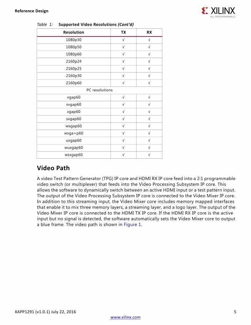
• Video resolutions up to UHD at @ 60 Hz (both at input and output interface), see Table 1.
• Video encoding RGB 4:4:4, YUV 4:4:4, and YUV 4:2:2.
• Interlaced input support: 1080i only.
• Supported use cases:
° Color space (RGB/YUV) and format (YUV 4:4:4/4:2:2) conversion.
° Scale up and down up to 4k2k at 60 Hz.
° Zoom mode: crops a user-defined window within the input stream and scales it to panel resolution.
° Picture-in-picture (PIP) mode: the input stream is scaled down to a user-defined window size and displayed at the user-defined coordinates on the panel.
° Ability to paint the PIP background to a defined color.
° Interlaced to progressive conversion.
° Frame rate conversion:
- Drop frames if input rate > output rate.
- Repeat frames if output rate < input rate.
The reference design can receive and transmit many different resolutions as listed in Table 1.
Video PathA video Test Pattern Generator (TPG) IP core and HDMI RX IP core feed into a 2:1 programmable video switch (or multiplexer) that feeds into the Video Processing Subsystem IP core. This allows the software to dynamically switch between an active HDMI input or a test pattern input. The output of the Video Processing Subsystem IP core is connected to the Video Mixer IP core. In addition to this streaming input, the Video Mixer core includes memory mapped interfaces that enable it to mix three memory layers, a streaming layer, and a logo layer. The output of the Video Mixer IP core is connected to the HDMI TX IP core. If the HDMI RX IP core is the active input but no signal is detected, the software automatically sets the Video Mixer core to output a blue frame. The video path is shown in Figure 1.
Memory SubsystemThe memory subsystem consists of an AXI-MM interconnect 6:1 crossbar that feeds into the Xilinx Memory Interface Generator (MIG). The six ports feeding into the crossbar are the data and instruction cache ports from the MicroBlaze processor, the memory port of the Video Processing Subsystem IP core, and three layers from the Video Mixer IP. The MIG bus is configured to be 512 bits wide. The net maximum bandwidth requirements of the video data are 4.75 GB/s:
• 4 GB/s for 3840x2160x60 Hz write to memory and read from memory at 32 bits/pixel.
• 0.75 GB/s for 1920x1080ix60 Hz write to memory and 2x1920x1080ix60 Hz read from memory at 32-bits/pixel.
Processor SubsystemA MicroBlaze processor is used to control the IP cores. The reference design uses the default configuration that is not optimized for performance because CPU load is not critical. The MicroBlaze processor has 8 KB of data and instruction caches. The MicroBlaze processor is run at a 100 MHz clock speed.
ClockingThe Video Processing Subsystem IP core uses three clocks that are derived through a clock generator from the 200 MHz system clock on the Kintex-7 FPGA KC705 board. The memory subsystem is running at this system clock at 200 MHz. This system clock feeds into the Clock Wizard IP, which derives a 300 MHz and a 100 MHz clock at the output. The 300 MHz clock drives the AXI4-Stream video interfaces. With the video processing IP subcores configured as two pixel per clock engines, a throughput of 600 megapixels is obtained. The 100 MHz clock drives the AXI4-Lite control interface and also drives the MicroBlaze processor.
The Video PHY core requires one GT reference clock for the HDMI TX core. The clock is generated by an external programmable clock generator. In the reference design, the SI5324 is used. This device is programmable through an I2C interface. The Video PHY core has two transceiver reference clocks for the HDMI RX core. The RX clock from the HDMI cable is connected to the first transceiver reference clock input. The second transceiver reference clock comes from an external free-running 125 MHz clock. This clock is used by the non-integer data recovery unit (NI-DRU) to recover low HDMI line rates that are below the minimum rate supported by the receive phase-locked loop (PLL).
Additional CoresIn addition to the V_PROC_SS, V_MIXER, VPHY, HDMI_TX_SS, and HDMI_RX_SS cores, the reference design includes these cores (see Figure 2):
Software ApplicationThe reference design incorporates the HDMI RX/TX connectivity IP cores to transmit native video in and out of the FPGA. The Video Processing Subsystem and Mixer IP cores form a processing chain that performs transformations on the incoming video. The MicroBlaze processor is the host CPU used in the design along with support peripherals, such as UART, I2C, and interrupt controller. The software view of the pipeline is shown in Figure 3.
The application software architecture is modular and provides the required separation between input, output, and the processing pipeline. The application software can be scaled to include additional input/output connectivity IP cores, such as DP or SDI.
The application software is comprised of these sub-blocks:
• Main
This block is the starting point for the application. It connects all of the block drivers according to the defined hardware pipeline and, subsequently, initializes and starts the pipeline.
After starting the processing chain, control transfers to the static scheduler (while(1) loop) that continuously monitors the system for user interaction, either from a serial terminal or from an external stimuli (interrupts triggered by input/output frequency change).
This block manages the input domain of the design and is responsible for initializing and bringing up the connectivity IP cores (for example, HDMI RX IP), including any board peripheral required by the input domain. Application-level callback functions required by the included IP core drivers are also implemented with this block.
This block exposes the system input interface structure so the user can define the connectivity IP core to be used in the design. Also, the user can define the associated APIs for the system to perform basic operations, such as initialize, start, or stop the input domain; set active inputs (design contains TPG as alternate input source); and query the IP core driver for detected streams.
Source Files: src/inpss/ -> xinss.c/h
• Output Subsystem
This block manages the output domain of the design. It initializes and brings up the backend IP cores (e.g., HDMI TX), including any board peripheral (e.g., DP159, SI5324) required by the output domain. Application-level callback functions required by the included IP core drivers are also implemented in this block.
This block exposes the system output interface so the user can define the connectivity IP core to be used in the design. Also, the user can define the associated APIs for the system to perform basic operations, such as initialize, start, and stop the output domain; set active outputs (if >1 present in the design); and set system output resolution. This block also includes the blender IP core (video mixer).
FPGA transceivers are tightly coupled with the connectivity MAC layer (e.g., HDMI RX/TX). This block manages the physical layer of the design. It initializes and brings up the transceivers. Application-level callback functions required by the Phy drivers are also implemented in this block.
Source Files used: src/phy -> physs.c/h
• Resources
This block manages the peripheral IP cores included in the design. It initializes and brings up the UART, Interrupt Controller, Test Pattern Generator, input/output muxes (if present), and the system timer. APIs are provided to control and configure the individual components when required.
IP DriversThe IP core drivers included in the board support package (BSP) for each of the video IP cores, abstract the internal complexity of the core. The drivers provide an out-of-the box solution for the core functionality with an easy-to-use functional API interface.
The drivers for an IP core with an interrupt source provide a mechanism for the user application to be notified of the event. The driver API allows for registering a function to be called when the particular interrupt occurs and before the control is transferred back to the application context.
Note: These callback functions are implemented at the user application level in the design and can serve as a reference for integrating the required IP cores in user-specific designs. For details on the specific IP driver integration requirements and suggestions, see the applicable IP core product guide.
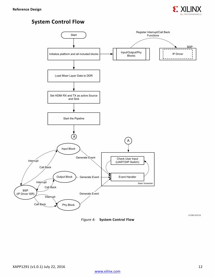
The steps in the system control flow are described in this section.
1. The main program is started with these initialization tasks:
° Define objects for each IP block driver (input/output/phy/peripherals).
° Initialize platform and enable data and instruction caches.
° Bind the objects to the system input/output/phy interfaces.
° Initialize all the blocks including board peripherals. During this step each block registers required or optional callback functions (e.g., HDMI RX/TX cable connect/disconnect, frequency change, etc.)
2. The video mixer layer data is preloaded into external memory during boot up from the embedded image data in source files, which is then sourced by the mixer IP every frame.
3. The processing pipeline is started with the default input and output resolution set to 1080p at 60 Hz RGB.
4. At power on, if no input is detected at the HDMI RX, the output video is muted to maintain stable output on the screen. The default is a solid blue frame.
5. The static scheduler (background task) continuously monitors the system for user input (via serial terminal) and reacts to external interrupts to configure the video pipe accordingly.
° When an interrupt occurs, control transfers to the source IP driver interrupt status register (ISR). Before the control returns to the user application, the registered callback is executed. The application logs the change by posting an event.
° The event handler processes the events in the preset priority order.
° The serial terminal parser decodes user commands and initiates the requested action.
FeaturesThe reference design demonstrates these features of the included video IP cores:
• Auto detect input resolution change and configure the video pipe.
• Auto detect "No Input" condition and mute output video.
• Supports crop, zoom, and PIP functionality.
• Read three video layers from memory and compose an output frame with four windows blended with master stream layer (HDMI RX stream).
• Support for many input and output resolutions up to 4K2K @ 60 Hz.
• Video processing functions, such as deinterlacing, color space and format conversions, scaling, letterboxing, etc.
• Includes alternate input source (TPG) to bring up the design even when no input source is available.
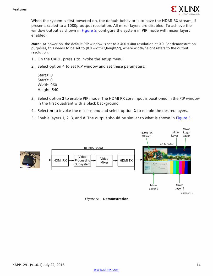
When the system is first powered on, the default behavior is to have the HDMI RX stream, if present, scaled to a 1080p output resolution. All mixer layers are disabled. To achieve the window output as shown in Figure 5, configure the system in PIP mode with mixer layers enabled:
Note: At power on, the default PIP window is set to a 400 x 400 resolution at 0,0. For demonstration purposes, this needs to be set to {0,0,width/2,height/2}, where width/height refers to the output resolution.
1. On the UART, press s to invoke the setup menu.
2. Select option 4 to set PIP window and set these parameters:
StartX: 0StartY: 0Width: 960Height: 540
3. Select option 2 to enable PIP mode. The HDMI RX core input is positioned in the PIP window in the first quadrant with a black background.
4. Select m to invoke the mixer menu and select option 1 to enable the desired layers.
5. Enable layers 1, 2, 3, and 8. The output should be similar to what is shown in Figure 5.X-Ref Target - Figure 5
HardwareThe hardware requirements for this reference system are:
• Xilinx Kintex-7 FPGA KC705 Evaluation Kit.
• One inrevium HDMI 2.0 daughter card (TB-FMCH-HDMI4K).
• Two HDMI cables.
• HDMI 2.0 video source (e.g., DVD Player).
• HDMI 2.0 sink (e.g., ultra HD TV set).
• JTAG USB Platform cable or USB cable Type-A to micro-B.
• USB cable with Type A to mini B.
SoftwareThe software requirements for this reference design are:
• Vivado Design Suite 2016.2.
• Software Development Kit (SDK) 2016.2.
• Software terminals (for example, Tera Term, HyperTerminal, or PuTTY).
External MemoryThree components in the reference design require external memory. The requirements for each are described in this section.
• The Video Processing Subsystem IP needs to store frames into DDR to perform frame rate conversions by the frame drop/repeat method, and also requires field buffers for the video deinterlacer. The buffer requirements are:
° Five UHD (4096x2160) buffers at max 48 bit/pixel = 265 MB
° Three 1080i field buffers at max 48 bit/pixel = 18 MB
Total memory required for Video Processing Subsystem buffer storage = 283 MB.
• The Video Mixer IP core in the design is preconfigured with three memory layers, a logo layer, and the main streaming layer. Typically, there are multiple sources (e.g., GPU, second input source, such as DP/SDI, etc.) that generate data for the mixer memory layer. However, the reference design does not have this source, so the mixer layer image data is included as a C source file and is compiled into the application binary. The details of each layer data are:
° Layer 1 is a 1600x542 resolution image. Every frame rendered on the screen is a consecutive subset (960x540) of the image, offset from the previous location in the image. On screen this appears as an image that is panned from left to right.
Memory required = 1600*542*32 bits = 3.5 MB
° Layer 2 is a graphics image of 960x540 resolution.
Memory required = 960x540*32 bits = 2 MB
° Layer 3 is a color bar test pattern, generated on-the-fly at power on by the included test pattern generator module, configured for 960x540 resolution.
Memory required = 960x540*32 bits = 2 MB
° Logo data is loaded into the block RAM allocated inside the IP core. No external memory is needed.
The total memory required for the Video Mixer IP core layer data storage = 7.5 MB.
Note: The static images resolution, embedded in the application software, is optimized for output resolution ≥ 1080p. If output resolution < 1080p is selected, the Video Mixer IP core image will not work.
• The application software binary is approximately 9 MB (800 KB of text and 7.5 MB of video mixer image data) and runs out of DDR. At power on, the application software loads the image data into the defined mixer layer buffer addresses in DDR.
The reference design memory storage requirement is ~300 MB.
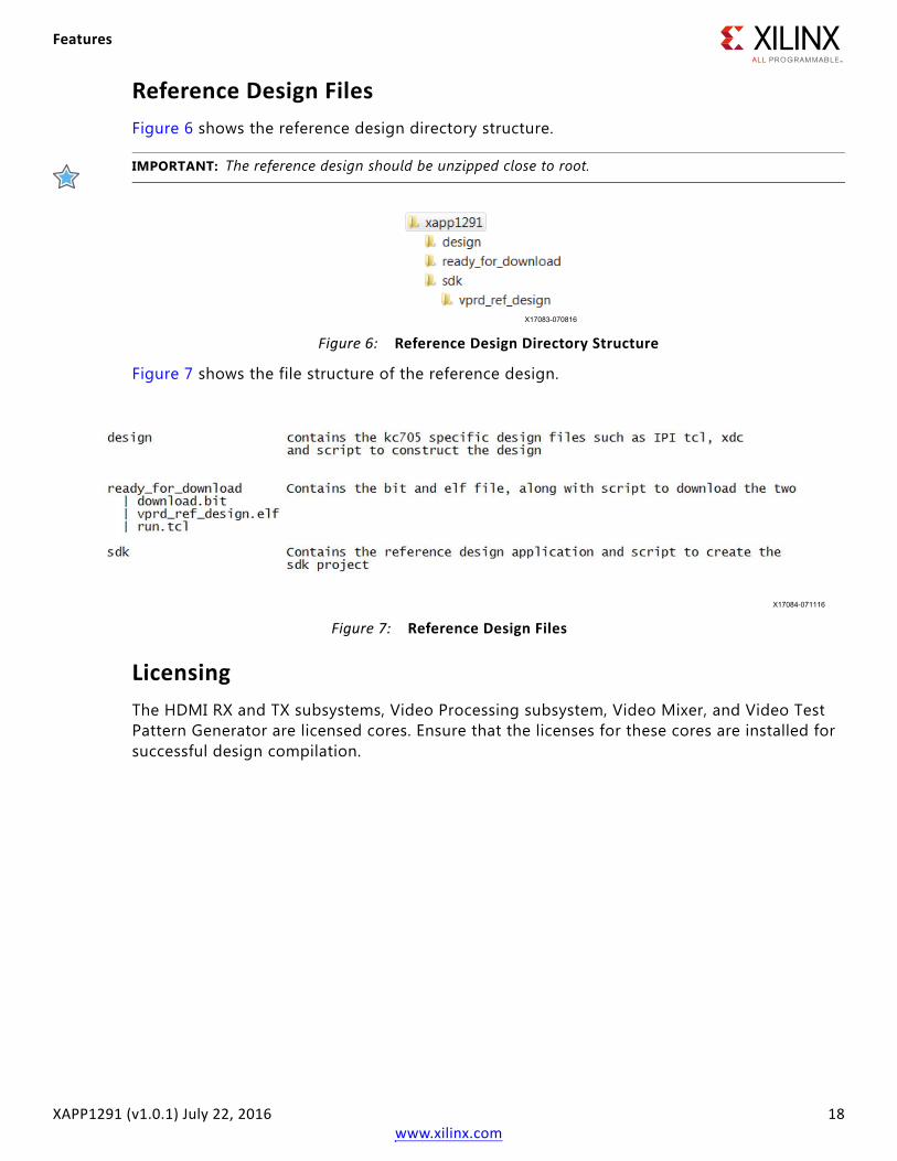
Reference Design FilesFigure 6 shows the reference design directory structure.
IMPORTANT: The reference design should be unzipped close to root.
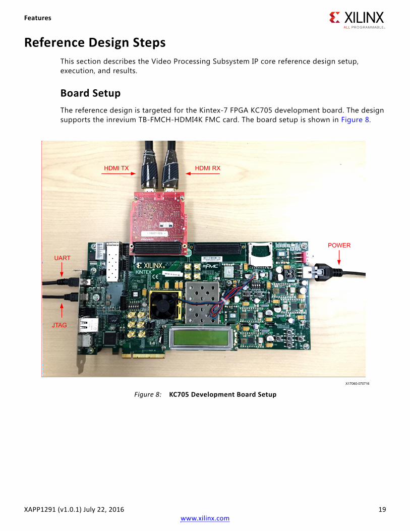
Figure 7 shows the file structure of the reference design.
LicensingThe HDMI RX and TX subsystems, Video Processing subsystem, Video Mixer, and Video Test Pattern Generator are licensed cores. Ensure that the licenses for these cores are installed for successful design compilation.
Reference Design StepsThis section describes the Video Processing Subsystem IP core reference design setup, execution, and results.
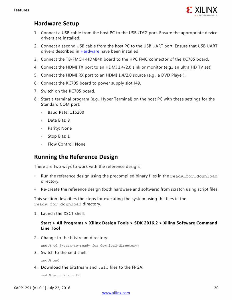
Board SetupThe reference design is targeted for the Kintex-7 FPGA KC705 development board. The design supports the inrevium TB-FMCH-HDMI4K FMC card. The board setup is shown in Figure 8.
IMPORTANT: The software application starts immediately after the completion of the FPGA configuration. Messages displayed on the serial terminal show the progress of the application powering up.
Creating the Reference Design Using Script Files
For users who prefer to create the design from scratch, TCL scripts (compatible with the Vivado 2016.2 tools) are provided in the design folder. The setup.tcl file generates an example design for the KC705 board with the FMC HDMI 2.0 card.
Building the Hardware Design
To generate the bit file in the Vivado Design Suite 2016.2:
1. Open the Vivado Design Suite.
2. At the Tcl console, change to the workspace directory:
> cd <unzip_dir>\xapp1291
3. Run the Tcl script to create the block design:
> source ./design/setup.tcl
4. Generate the bitstream by clicking Generate Bitstream from the Flow menu.
IMPORTANT: The bitstream generation can take about an hour to complete on a typical Windows-based computer.
5. Export the hardware to SDK by selecting File > Export > Export Hardware. Select the option to include the bitstream. This creates a vprd.sdk directory under the Vivado project directory and exports the Xilinx platform project file into the directory.
Known Issues
• The design fails to meet timing during compilation and is a known issue with the Video Mixer core. The Video Mixer core is in early access. This issue will be addressed in the Vivado Design Suite 2016.3 release. A workaround is to disable the logo layer in the Video Mixer to remove timing violations.
• The Vivado Design Suite on computers running Windows is sensitive to project path length. To avoid any path length issues, unzip the design to c:\.
The SDK folder has a script (vprd.tcl) that automates the process of creating an SDK project for the reference design and generating the downloadable .bit and .elf files.
To run the provided Tcl script:
1. Copy the exported hardware design file (vprd_wrapper.hdf) to the sdk folder.
2. Launch the Xilinx Software Command Line Terminal (XSCT) shell:
Start > All Programs > Xilinx Design Tools > SDK 2016.2 > Xilinx Software Command Line Tool
3. Change to the sdk directory:
xsct% cd {<path-to-sdk-directory>}
4. Source the tcl file
xsct%>source vrpd.tcl
5. Execute the script:
xsct%>vprd vprd_wrapper.hdf
The Tcl script performs these tasks:
• Creates workspace.
• Creates hardware project.
• Creates BSP.
• Creates application project.
• Builds BSP and application project.
After the process is complete, the required files are available here:
• Bit file is available in the vrpd.sdk/vprd_kc705_hw_platform_0 folder.
• Elf file is available in the vprd.sdk/vprd_ref_design/{Debug/Release} folder.
Perform these steps to run the software application from within the SDK:
IMPORTANT: Make sure the hardware is powered on and a Digilent Cable or an USB platform cable is connected to the host PC. Also, ensure that a USB cable is connected to the UART port of the KC705 board.
1. Launch SDK.
2. Set workspace to the vprd.sdk folder in the prompted window. The SDK project opens automatically (if a welcome page appears, close it.)
3. Download the bitstream into the FPGA by selecting Xilinx Tools > Program FPGA. The program FPGA dialog box opens.
4. Ensure that the bitstream field shows the bitstream file generated by the Tcl script, and then click Program.
Note: The DONE LED on the board turns green if the programming is successful.
5. A terminal program (HyperTerminal or PuTTY) is needed for UART communication. Open the program, choose the appropriate port, set baud rate to 115 kb/s, and establish the serial port connection.
6. Select and right-click the application vprd_ref_design in the Project_Explorer panel.
7. Select Run As > Launch on Hardware (System Debugger).
8. Select Binaries and Qualifier in the window and click OK.
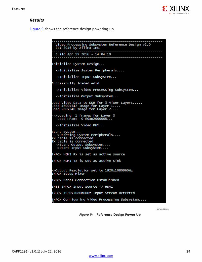
The design execution progress is shown in the terminal program.
User InterfaceThe video processing reference design (VPRD) provides two interfaces for interacting with the design:
• Serial terminal.
• Pushbuttons.
Serial Terminal (UART)A serial terminal interface is provided for interacting with the design. Connect the host computer to the USB UART, open the terminal, and set the terminal properties to 115200 baud rate, 8 data bits, no parity, and 1 stop bit.
After the application has been downloaded to the FPGA, the serial terminal prints a welcome message and shows the progress.
UART Menus
The reference design functionality can be accessed through the serial terminal. There are different menus available for each feature. The 'h' key displays the help menu, which lists all of the feature menus available in the reference design.
Note: The menu selection keys are not case sensitive.X-Ref Target - Figure 10
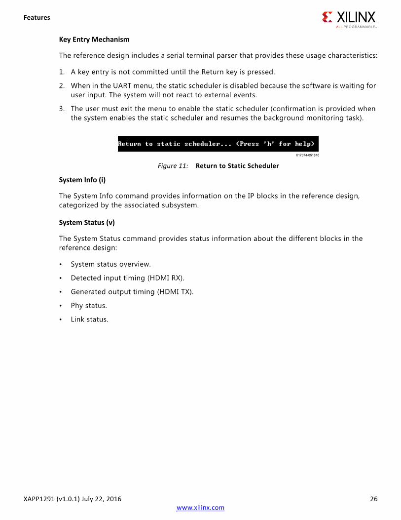
The reference design includes a serial terminal parser that provides these usage characteristics:
1. A key entry is not committed until the Return key is pressed.
2. When in the UART menu, the static scheduler is disabled because the software is waiting for user input. The system will not react to external events.
3. The user must exit the menu to enable the static scheduler (confirmation is provided when the system enables the static scheduler and resumes the background monitoring task).
System Info (i)
The System Info command provides information on the IP blocks in the reference design, categorized by the associated subsystem.
System Status (v)
The System Status command provides status information about the different blocks in the reference design:
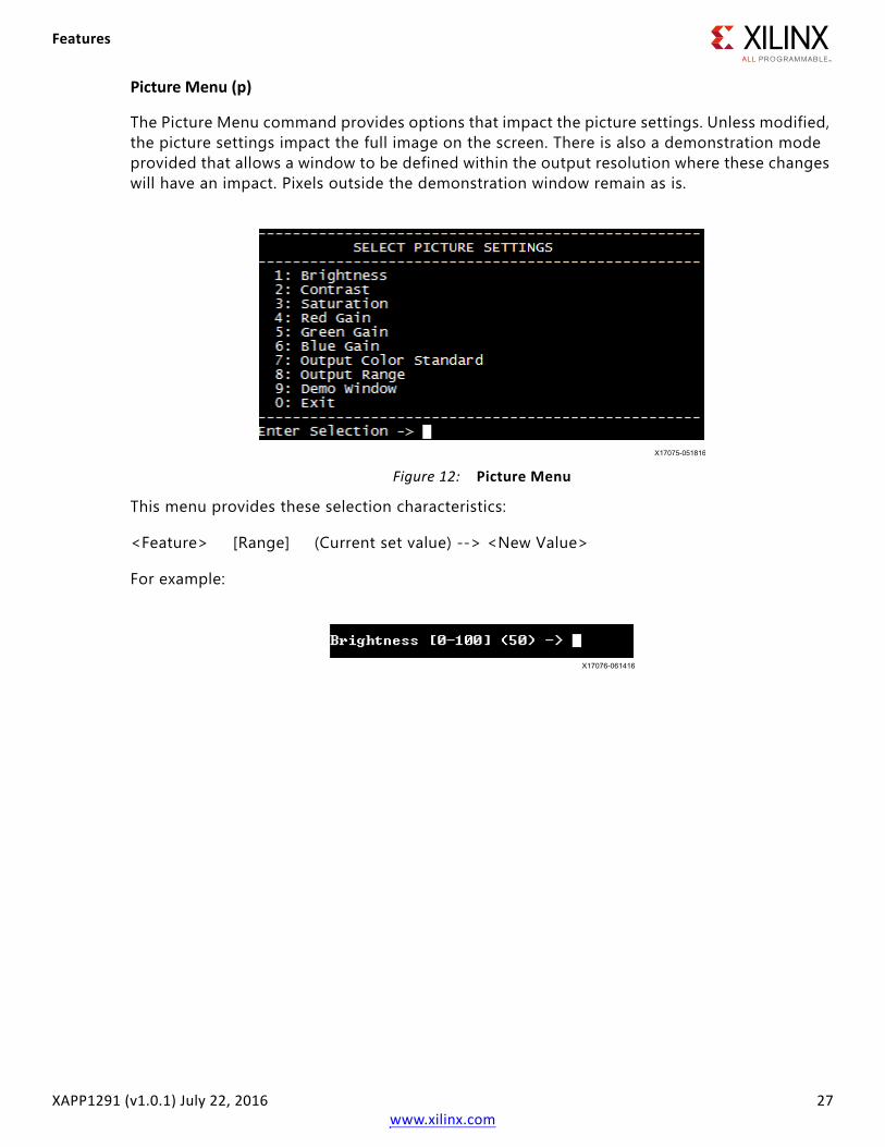
The Picture Menu command provides options that impact the picture settings. Unless modified, the picture settings impact the full image on the screen. There is also a demonstration mode provided that allows a window to be defined within the output resolution where these changes will have an impact. Pixels outside the demonstration window remain as is.
This menu provides these selection characteristics:
<Feature> [Range] (Current set value) --> <New Value>
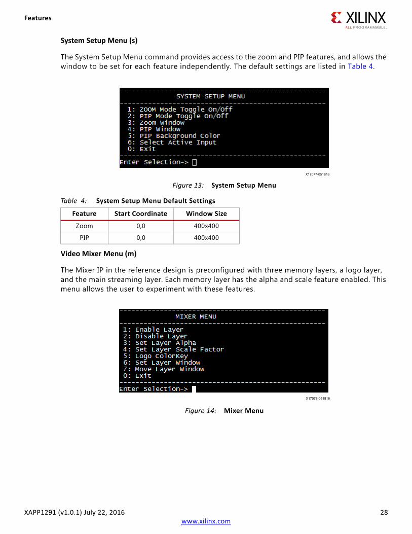
The System Setup Menu command provides access to the zoom and PIP features, and allows the window to be set for each feature independently. The default settings are listed in Table 4.
Video Mixer Menu (m)
The Mixer IP in the reference design is preconfigured with three memory layers, a logo layer, and the main streaming layer. Each memory layer has the alpha and scale feature enabled. This menu allows the user to experiment with these features.
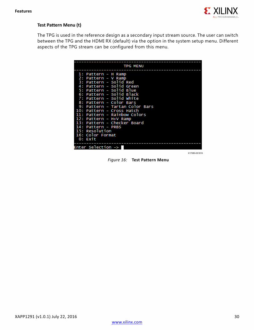
The TPG is used in the reference design as a secondary input stream source. The user can switch between the TPG and the HDMI RX (default) via the option in the system setup menu. Different aspects of the TPG stream can be configured from this menu.
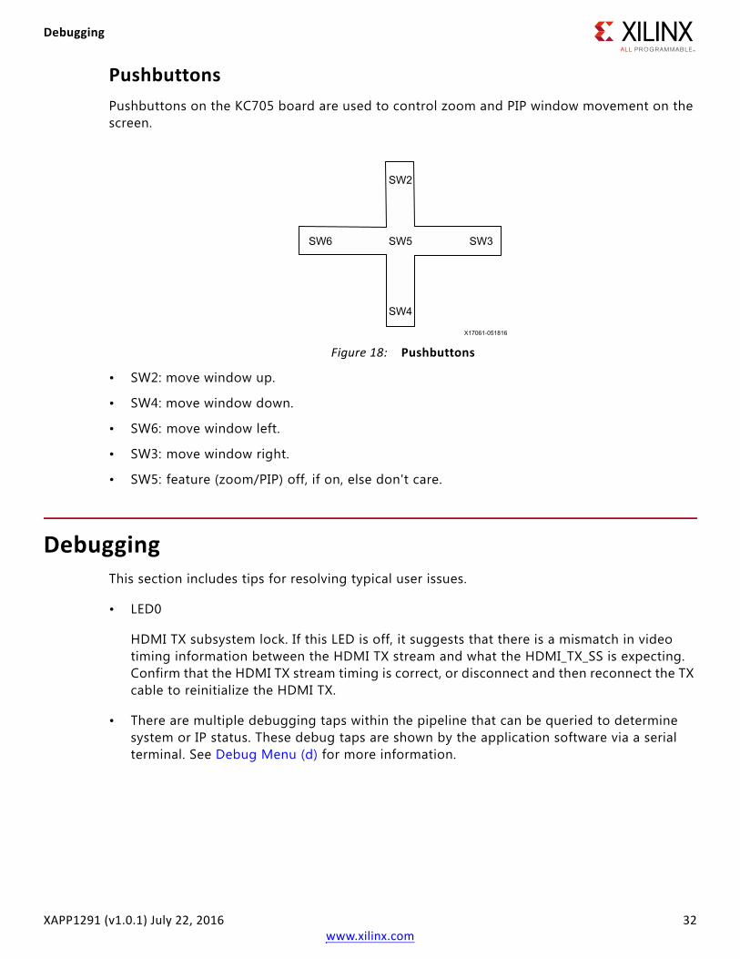
PushbuttonsPushbuttons on the KC705 board are used to control zoom and PIP window movement on the screen.
• SW2: move window up.
• SW4: move window down.
• SW6: move window left.
• SW3: move window right.
• SW5: feature (zoom/PIP) off, if on, else don't care.
DebuggingThis section includes tips for resolving typical user issues.
• LED0
HDMI TX subsystem lock. If this LED is off, it suggests that there is a mismatch in video timing information between the HDMI TX stream and what the HDMI_TX_SS is expecting. Confirm that the HDMI TX stream timing is correct, or disconnect and then reconnect the TX cable to reinitialize the HDMI TX.
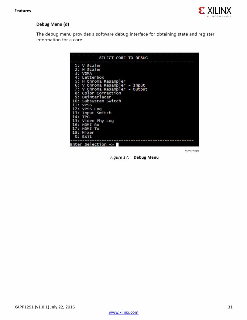
• There are multiple debugging taps within the pipeline that can be queried to determine system or IP status. These debug taps are shown by the application software via a serial terminal. See Debug Menu (d) for more information.
Revision HistoryThe following table shows the revision history for this document.
Please Read: Important Legal NoticesThe information disclosed to you hereunder (the “Materials”) is provided solely for the selection and use of Xilinx products. To the maximum extent permitted by applicable law: (1) Materials are made available "AS IS" and with all faults, Xilinx hereby DISCLAIMS ALL WARRANTIES AND CONDITIONS, EXPRESS, IMPLIED, OR STATUTORY, INCLUDING BUT NOT LIMITED TO WARRANTIES OF MERCHANTABILITY, NON-INFRINGEMENT, OR FITNESS FOR ANY PARTICULAR PURPOSE; and (2) Xilinx shall not be liable (whether in contract or tort, including negligence, or under any other theory of liability) for any loss or damage of any kind or nature related to, arising under, or in connection with, the Materials (including your use of the Materials), including for any direct, indirect, special, incidental, or consequential loss or damage (including loss of data, profits, goodwill, or any type of loss or damage suffered as a result of any action brought by a third party) even if such damage or loss was reasonably foreseeable or Xilinx had been advised of the possibility of the same. Xilinx assumes no obligation to correct any errors contained in the Materials or to notify you of updates to the Materials or to product specifications. You may not reproduce, modify, distribute, or publicly display the Materials without prior written consent. Certain products are subject to the terms and conditions of Xilinx’s limited warranty, please refer to Xilinx’s Terms of Sale which can be viewed at http://www.xilinx.com/legal.htm#tos; IP cores may be subject to warranty and support terms contained in a license issued to you by Xilinx. Xilinx products are not designed or intended to be fail-safe or for use in any application requiring fail-safe performance; you assume sole risk and liability for use of Xilinx products in such critical applications, please refer to Xilinx’s Terms of Sale which can be viewed at http://www.xilinx.com/legal.htm#tos.AUTOMOTIVE APPLICATIONS DISCLAIMERAUTOMOTIVE PRODUCTS (IDENTIFIED AS "XA" IN THE PART NUMBER) ARE NOT WARRANTED FOR USE IN THE DEPLOYMENT OF AIRBAGS OR FOR USE IN APPLICATIONS THAT AFFECT CONTROL OF A VEHICLE ("SAFETY APPLICATION") UNLESS THERE IS A SAFETY CONCEPT OR REDUNDANCY FEATURE CONSISTENT WITH THE ISO 26262 AUTOMOTIVE SAFETY STANDARD ("SAFETY DESIGN").