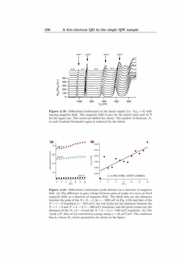
DOTTORATO DI RICERCA IN FISICA – XIX CICLO sede amministrativa UNIVERSIT ` A DEGLI STUDI DI MODENA E REGGIO EMILIA TESI PER IL CONSEGUIMENTO DEL TITOLO DI DOTTORE DI RICERCA Transport properties of InGaAs based devices CANDIDATO: Daniele Ercolani Universit` a di Modena e Reggio Emilia RELATORE: Prof. Lucia Sorba Universit` a di Modena e Reggio Emilia
Transcript
DOTTORATO DI RICERCA IN FISICA – XIX CICLO
sede amministrativaUNIVERSITA DEGLI STUDI DI MODENA E REGGIO EMILIA
TESI PER IL CONSEGUIMENTO DEL TITOLO DI DOTTORE DIRICERCA
Transport properties of InGaAsbased devices
CANDIDATO:
Daniele Ercolani
Universita di Modena e Reggio Emilia
RELATORE:
Prof. Lucia Sorba
Universita di Modena e Reggio Emilia
Foreword
Even though only my name is printed on the cover of this booklet, it isthe result of the joint effort of a multitude of people. First of all I mustthank my tutor, Lucia Sorba, for the constant support given to me in allthese years. Her help has definately not been limited to scientific adviceand tutoring, but has ranged from waking me up in the morning when Islept too late to taking care of annoying paperwork at the University ofModena. She has bought without a blink countless liters of liquid heliumeven when results to be obtained were uncertain, has stayed up late inthe laboratory to discuss and correct my work, answered stupid questions,fought continously with her enormous energy against all bureocratic andtechnical difficulties encountered, and has withstood my attitude, even inthese last, frenetic months. Thank you very much, Lucia. Next, the otherpresent and past group members: Giorgio Biasiol, the growth-master, for theexceptional samples grown at will, and the many suggestions and dropletsof scientific wisdom on all aspects of the growth; Flavio Capotondi, who’sdone the hard work on the InGaAs samples back when they were still a totalmystery, with his stakanovism, long nights and weekends in the laboratoryand in the cleanroom, and his curious mind about all aspect of physics. Andabout beer. My lab-brother Giorgio Mori, whom I cannot praise enough,for the endless discussions on the meaning of life, the universe and all therest (including physics). Marco Lazzarino, the wizard who has introducedall of us to the black magic of processing and fabrication, with enthusiasmand dedication, and for all the talks about politics, mountains, travels, food,life, etc. Silvano De Franceschi, with his jolly attitude and religious passionabout magnetotransport on nanothings, for coping with my ignorance anddisbelief and shading light in this “Coulomb what?” thing. My fellow Ph.D.student Tomaz Mlakar, and the Ph.D.-student-to-be Massimo Mongillo fortheir help and support, especially in this last period of frenetic craziness.Last but not least, Stefan Heun, for many things among which the proof-reading of all the stuff that follws, back when it was still in beta version...
I must not forget the patience with which Luca Businaro has stuck inmy head the basic and advanced notions of EBL and SEM. Did I write‘patience’? Well... anyhow Luca has spent an enormous amount of timewith me, and by now I have learned to read the subtitles, so, yes, patience
Foreword
and attention. Thanks Luca. Actually I owe a lot also to many other Lilitgroup members, starting hierarchically from Stefano Cabrini down to thePh.D. students, Mauro Prasciolu (always available for advice and discus-sion, and always smiling), Radu, Arrigo, Matteo, and yes, also “la vita edura” Alessandro. And then come the people at the NEST in Pisa: “papa”Pasqualantonio Pingue whith his sardonic humor and all the help, sugges-tions, consulting, praying and swearing at the EBL (sorry again, Pask, forhitting the column with the sample holder!), and Franco Carillo, who alsohas always found five minutes for me when I needed, and more if I neededmore.
Special thanks to Ales, Federico and Paolino of the mechanical workshop:it is a pleasure to see them working with their hands and huge machinery tofabricate tiny, perfect, pieces of art. Always in good mood, rarely mistakenwhen giving suggestions on the design of things to be made, and really en-joying a work well done. Moreover, they have promptly saved me in severalsituations in which I urgently needed their help. Same goes for Stefano Bi-garan, the “everything” technician, the man who solves problems, who neversits, who brings back to life computers (and also kills them sometimes!). Andhow to forget the countless times that the electronics technicians Stefano,Fabio or Andrea have fixed some board, some controller, or resoldered thehorrible lump of wires of one of the low-temperature inserts!
I also have to mention the support I have recived in the other half of time,from my parents and their spouses, patient and understanding, to whom Iowe most, and from my friends, who are still my friends even though I’vebeen increasingly spending my time in the laboratory and less and less withthem. Thanks guys. At last Cecilia, the women I want to spend my life with,and who happens also to be my wife, deserves a very special aknowledgment.First, because she’s not asked to divorce yet, even though she has been morelike a widow for the past months, while I was measuring ans writing, callingat 10 P.M. saying “Sorry, sorry, I’ll be home in 15 minutes” and insteadarriving at after midnight; when I was writing or studying or even measuringalso in the weekends, not giving any help to solve problems at home or dohousework or preparing dinner, and so on. Second, because I would not evenhave graduated withour her support, pressure and deadlines. And last, forall the rest.
In synthesys, all these people (and others that I am certainly forget-ting now) deserve credit for the good things that may appear in the pagesthat follow. Mistakes, errors, and misinterpretations are, instead, my soleresponsability.
Semiconductor technology has revolutionized the second half of the twenti-eth century. Although the majority of the revolution has been based on sili-con, increasing demands in terms of speed and functionality have generatedinterest in alternative semiconductor materials. Most noteworthy amongthese are the compound semiconductors made of group III and group V ele-ments, of which GaAs and related alloys are the most developed. At present,III-V compound semiconductors provide the basis material for a number ofwell-established commercial technologies, as well as new cutting-edge classesof electronic and optoelectronic devices. Just a few examples include high-electron-mobility transistors and heterostructure bipolar transistors, diodelasers, light-emitting diodes, photodetectors, electro-optic modulators, andfrequency-mixing components. The operating characteristics of these de-vices depend critically on the physical properties of the constituent mate-rials, which are often combined in heterostructures containing carriers con-fined into regions of the order of a few nanometers.
One of the major advantages of ternary alloys with respect to binarycompounds is the possibility to tune, in the range defined by the constituentbinaries, their physical properties, such as band gap, effective mass, and theLande g-factor, by changing the alloy composition.
One of the most studied alloy systems, both for optical and electronicapplications, is InxGa1−xAs. At an indium concentration (x) of 0.53, thismaterial is lattice matched to InP and today largely used in light-emittersfor optical fiber communications since its emission wavelength of 1.55 µm iswithin the optimum transmission window of silica fibers.
For electronic applications, the possibility to suppress the Schottky bar-rier at the metal-semiconductor interface, by increasing the indium con-centration over 0.75, makes high In concentration InxGa1−xAs alloys theideal material to create highly transmissive junctions. This peculiar fea-ture makes this system appealing for studying the transport properties atsemiconductor/superconductor or semiconductor/ferromagnet junctions atlow temperatures. Furthermore, at high indium concentrations the Landeg-factor of the system increases towards the value of InAs (around -15); thusthe resulting large Zeeman spin splitting under the application of weak mag-netic fields makes this alloy a promising candidate for spin-valve mesoscopic
2 Introduction
devices working at relatively high temperatures.A major problem in the development of devices based on such alloys
is the lack of substrates with suitable lattice parameter. Consequently, inorder to realize structures with good electrical properties, a careful controlof structural defects, related to the strain relief, is necessary.
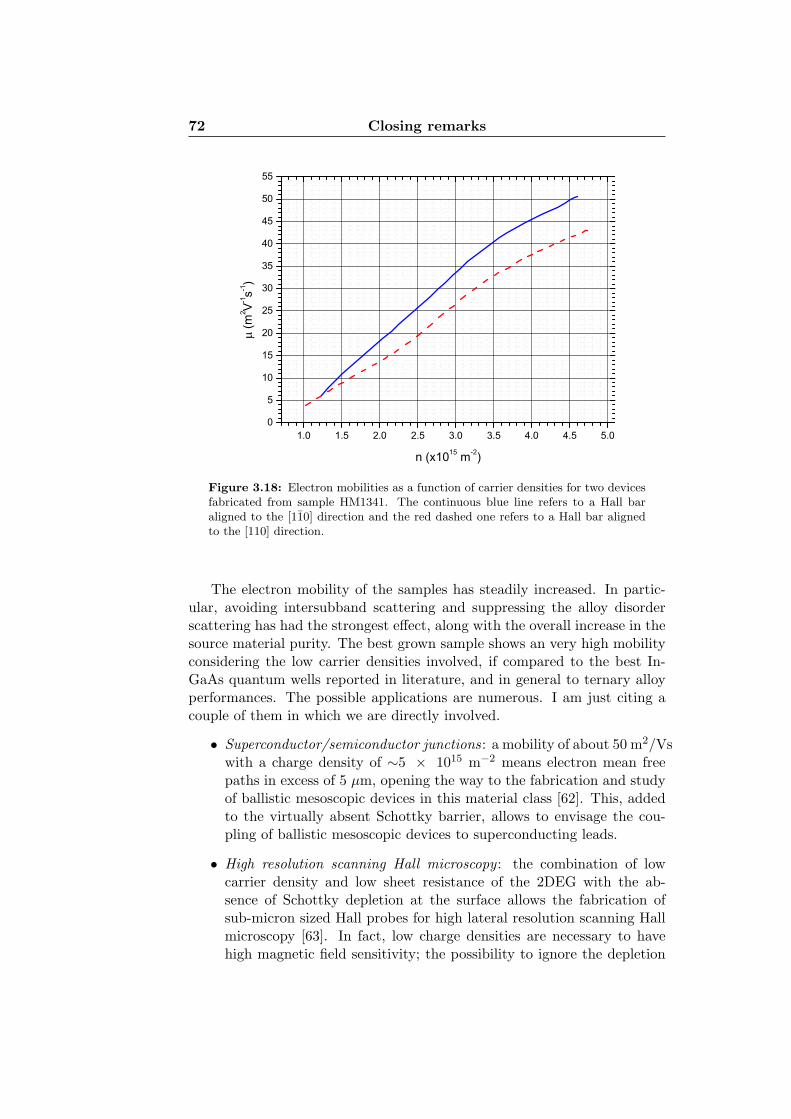
In this thesis, we have investigated the structural and transport proper-ties of two-dimensional electron gases formed in In0.75Ga0.25As/In0.75Al0.25Asquantum wells grown on GaAs (001) substrates. Using a graded buffer toaccommodate the lattice mismatch between GaAs and InxGa1−xAs, andinserting thin InAs layers in the quantum well to reduce alloy disorder scat-tering, we are able to obtain low temperature electron mobilities well above30 m2/Vs in unintentionally doped structures with a carrier density of theorder of 3 × 10¹⁵ m−2. By increasing the carrier density to ∼5 × 10¹⁵ m−2
with the aid of a top metal gate, the mobility can exceed 50 m2/Vs.In order to characterize such structures, several issues have been ex-
plored:
1. We have optimized the step-graded buffer layer structure employed toaccommodate the lattice mismatch between the GaAs substrate andthe InGaAs layer in order to minimize the residual strain inside theconductive channel. We found that a careful control of the residualstrain in the quantum well region is necessary to obtain a high electronmobility in such systems.
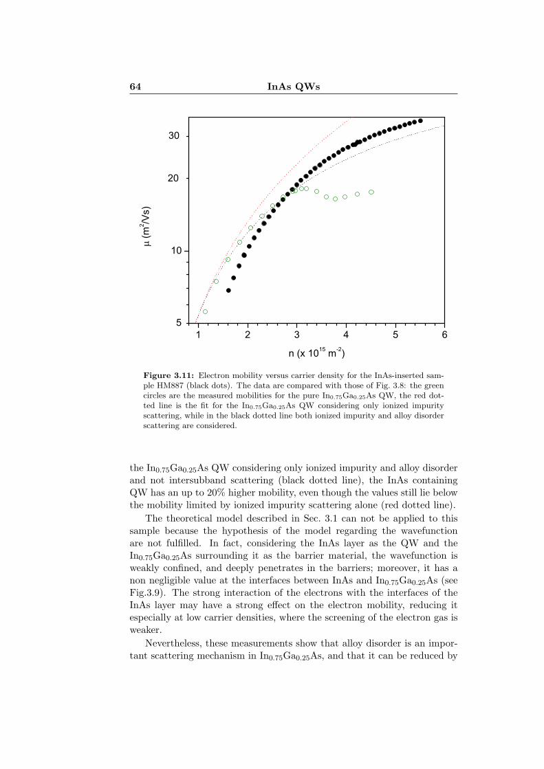
2. The scattering processes limiting the low temperature mobility in thesesystems are deduced from the dependence of the electron mobility onthe two-dimensional electron gas density. From such analysis we haveinferred that the mobility is essentially limited by background ionizedimpurities and by alloy scattering.
3. By partially suppressing these main scattering mechanisms the elec-tron mobility of the sample is increased to the extremely high valuesindicated above.
The electron mobilities achieved are high enough to envisage the fabricationof mesoscopic devices on these samples, such as quantum point contacts orquantum dots. In particular, few-electron quantum dots are thought to bethe basis for the practical realization of Qbits, the building blocks of quan-tum computers, using the spin degree of freedom as carrier of information.The high Lande g-factor of InxGa1−xAs would make spin manipulation inInxGa1−xAs based quantum dots much more efficient, with respect to GaAsbased quantum dots, in terms of the relaxation of both low temperature andhigh magnetic field requirements.
We have fabricated few-electron quantum dots with integrated chargereadout in lower indium concentration InxGa1−xAs quantum wells, mea-suring the electron g-factor and studying other spin-related issues, like the
Introduction 3
Kondo effect. We have also begun addressing the problems related withnanometer-sized Schottky gate fabrication on high indium concentrationInxGa1−xAs quantum well structures.
Chapter 1 of this thesis desctibes the growth procedure and characteri-zation techniques employed to study the InxGa1−xAs quantum well samplesand devices.
A thorough analysis of the structural properties of the InAlAs/InGaAsquantum wells and the relation between their structural and transport prop-erties are presented in chapter 2.
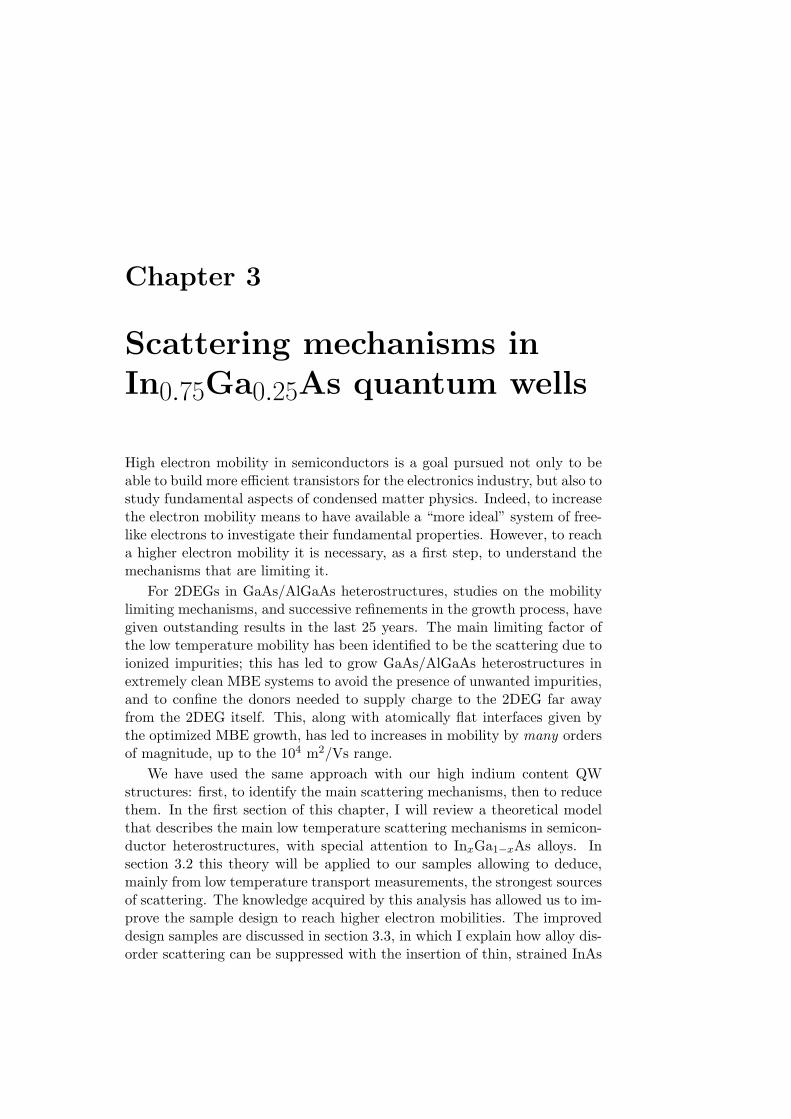
The dependence of the electron mobility on the carrier density is studiedin chapter 3 in order to determine the low temperature scattering processeslimiting the electron mobility. Several modifications to the sample designresulting from this analysis are shown and discussed, including the reductionof the quantum well width and the insertion of thin InAs layers in thequantum well.
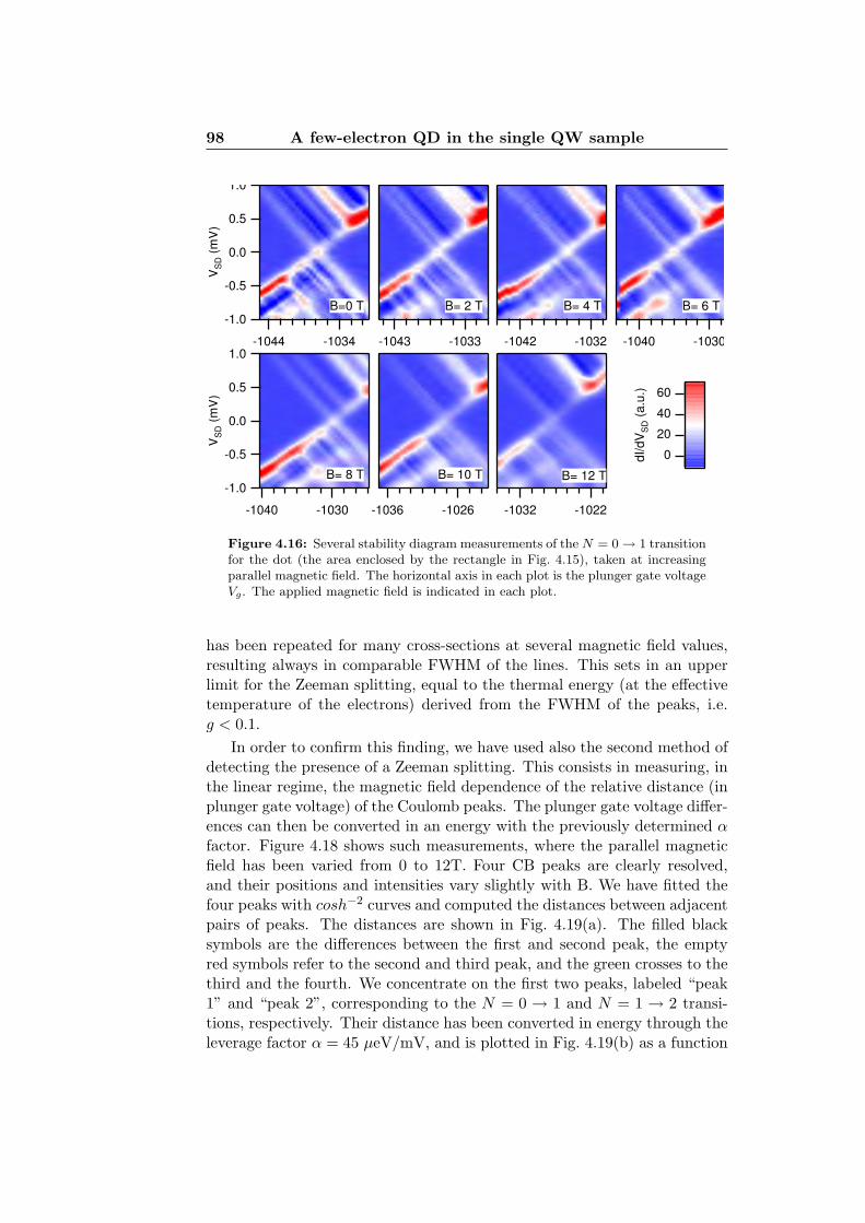
Chapter 4 is dedicated to the study of mesoscopic devices fabricatedfrom two-dimensional electron gases formed in InxGa1−xAs quantum wells.The concept of quantum computing is introduced, showing the need of elec-trically tuned few-electron semiconductor quantum dots. Low temperaturetransport experiments in low indium content, few electron quantum dotswith integrated charge readout are described, focusing on the spin effects.The Lande g-factor of the electrons in the quantum dots is measured, andthe Kondo effect in the weak coupling regime studied. To conclude with, theissues related to the fabrication of nanostructures on high indium contentsamples are addressed and discussed.
4 Introduction
Chapter 1
Instruments and Techniques
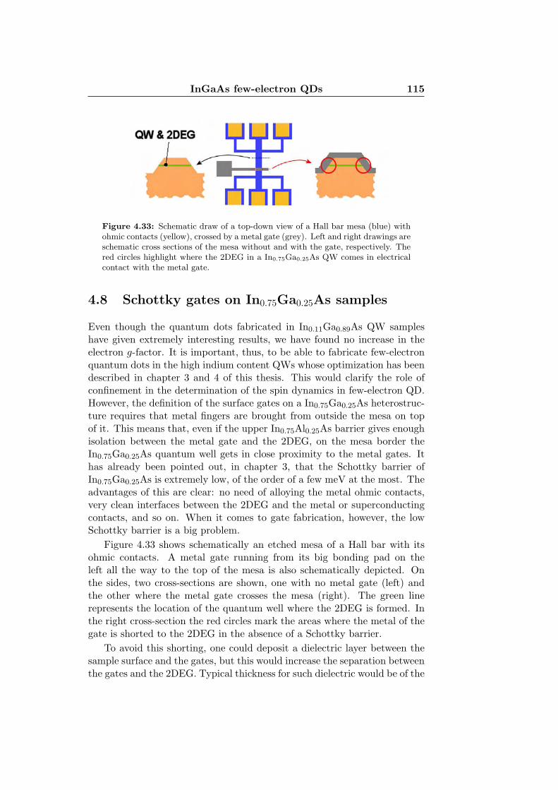
The aim of this chapter is to briefly describe the instruments and tech-niques employed in this thesis. The first section considers the basic prin-ciples of molecular beam epitaxy (MBE) and, in particular, focuses theattention on the MBE machine installed at the Laboratorio TASC INFM-CNR. Sections 1.2 and 1.3 describe the main morphological characteriza-tion techniques: first, high resolution X-Ray diffraction (XRD) which givesprecise quantitative information on the crystal structure and is of funda-mental importance for MBE growth calibration of indium alloys, and thenAtomic Force Microscopy, used to probe microscopically the topography ofsample surfaces. In section 1.4 the growth of InxGa1−xAs/InxAl1−xAs het-erostructures containing a two-dimensional electron gas is discussed, whilesection 1.5 is focused on the fabrication techniques that are used to patternsamples with Hall bar devices and nanometer sized top metal gates neededto perform transport measurements. Finally, Section 1.6 is dedicated to thedescription of the experimental setup used to perform transport measure-ments at cryogenic temperatures.
1.1 Molecular beam epitaxy
Molecular beam epitaxy (MBE) is an Ultra-High-Vacuum (UHV) basedtechnique for producing high quality epitaxial structures with monolayer(ML) control. Since its introduction in the 1970s as a tool for growing high-purity semiconductor films, MBE has evolved into one of the most widelyused techniques for producing epitaxial layers of metals, insulators, semi-conductors, and superconductors, both at the research and the industrialproduction level. The principle underlying MBE growth is relatively simple:it consists essentially in the production of atoms or clusters of atoms byheating of a solid source. They then migrate in an UHV environment andimpinge on a hot substrate surface, where they can diffuse and eventuallyare incorporated into the growing film. Despite the conceptual simplicity, a
6 Molecular beam epitaxy
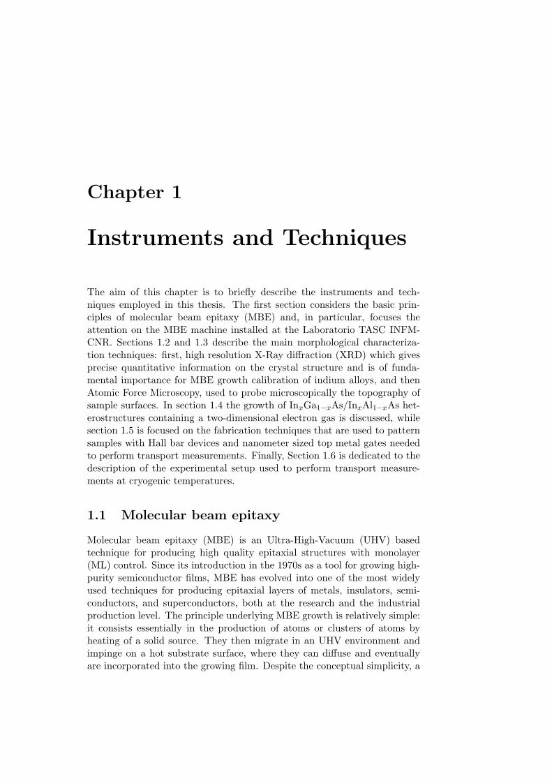
Figure 1.1: Schematic drawing of a generic MBE system (top view).
great technological effort is required to produce systems that yield the de-sired quality in terms of material purity, uniformity, and interface control.An exhaustive discussion on the principles and applications of the MBEtechnique can be found in Ref. [1].
The choice of MBE with respect to other growth techniques depends onthe desired structures and needs. In particular, MBE is the proper techniquewhen abruptness and control of interfaces and doping profiles are needed,thanks to the low growth temperature and rate. Besides, the control onthe vacuum environment and on the quality of the source materials allowsa much higher material purity, as compared to non UHV based techniques,especially in Al containing semiconductors for applications in high mobilityand high speed devices.
1.1.1 Growth apparatus
A schematic drawing of a standard MBE system is shown in Fig. 1.1. Somebasic components are:
• The vacuum system consists in a stainless-steel growth chamber, UHV-connected to a preparation chamber, where substrates are degassedprior to growth. All the components of the growth chamber mustbe able to resist bake-out temperatures of up to 200C for extendedperiods of time, which are necessary to minimize outgassing from the
Instruments and Techniques 7
internal walls.
• The pumping system must be able to efficiently reduce residual im-purities to a minimum. The pumping system usually consists of ionpumps, with auxiliary Ti-sublimation and cryogenic pumps, for thepumping of specific gas species. Typically the base pressure of anMBE chamber is from 10−11 to 10−12 mbar, which determines an im-purity concentration below 1015 cm−3 in grown structures.
• Liquid N2 cryopanels surround internally both the main chamber wallsand the source flanges. Cryopanels prevent re-evaporation from partsother than the hot cells and provide thermal isolation among the dif-ferent cells, as well as additional pumping of the residual gas.
• Effusion cells are the key components of a MBE system, because theymust provide excellent flux stability and uniformity, and material pu-rity. The cells (usually from six to ten) are placed on a source flange,and are co-focused on the substrate to optimize flux uniformity. Theflux stability must be better than 1% during a work day, with day-to-day variations of less than 5% [2]. This means that the temperaturecontrol must be of the order of ±1C at 1000C [1]. The material to beevaporated is placed in the effusion cells. A mechanical or pneumaticshutter, usually made of tantalum or molybdenum, is placed in frontof the cell, and it is used to trigger the flux coming from the cell (seeFig. 1.1).
• The substrate manipulator holds the wafer on which the growth takesplace. It is capable of a continuous azimuthal rotation around itsaxis to improve the uniformity across the wafer. The heater behindthe sample is designed to maximize the temperature uniformity andminimize power consumption and impurity outgassing. Opposite tothe substrate holder, an ionization gauge is placed which can be movedinto the molecular beam and is used as a beam flux monitor (BFM).
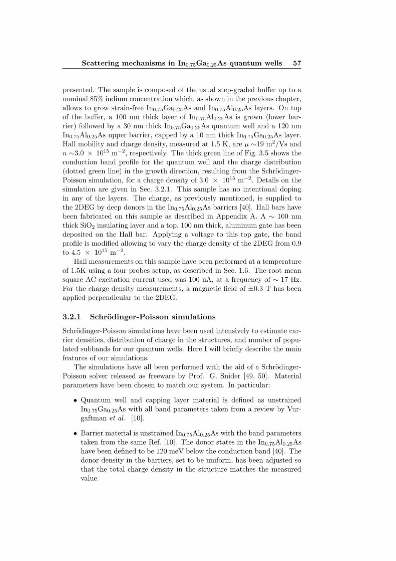
• The Reflected High Energy Electron Diffraction (RHEED) gun and de-tection screen are used to calibrate precisely the material fluxes evap-orated by the effusion cells; with RHEED it is possible to monitor theepitaxial growth monolayer by monolayer. A thorough description ofthis tool is given in section 1.1.3.
1.1.2 MBE growth process
In general, three different phases can be identified in the MBE process [1].The first is the crystalline phase constituted by the growing substrate, whereshort- and long-range order exists. On the other extreme, there is the disor-dered gas phase of the molecular beams. Between these two phases, there is
8 Molecular beam epitaxy
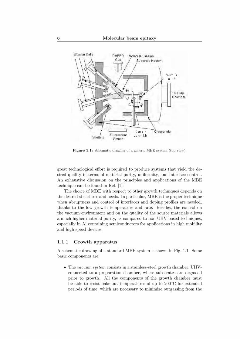
Figure 1.2: Different surface elemental processes in MBE.
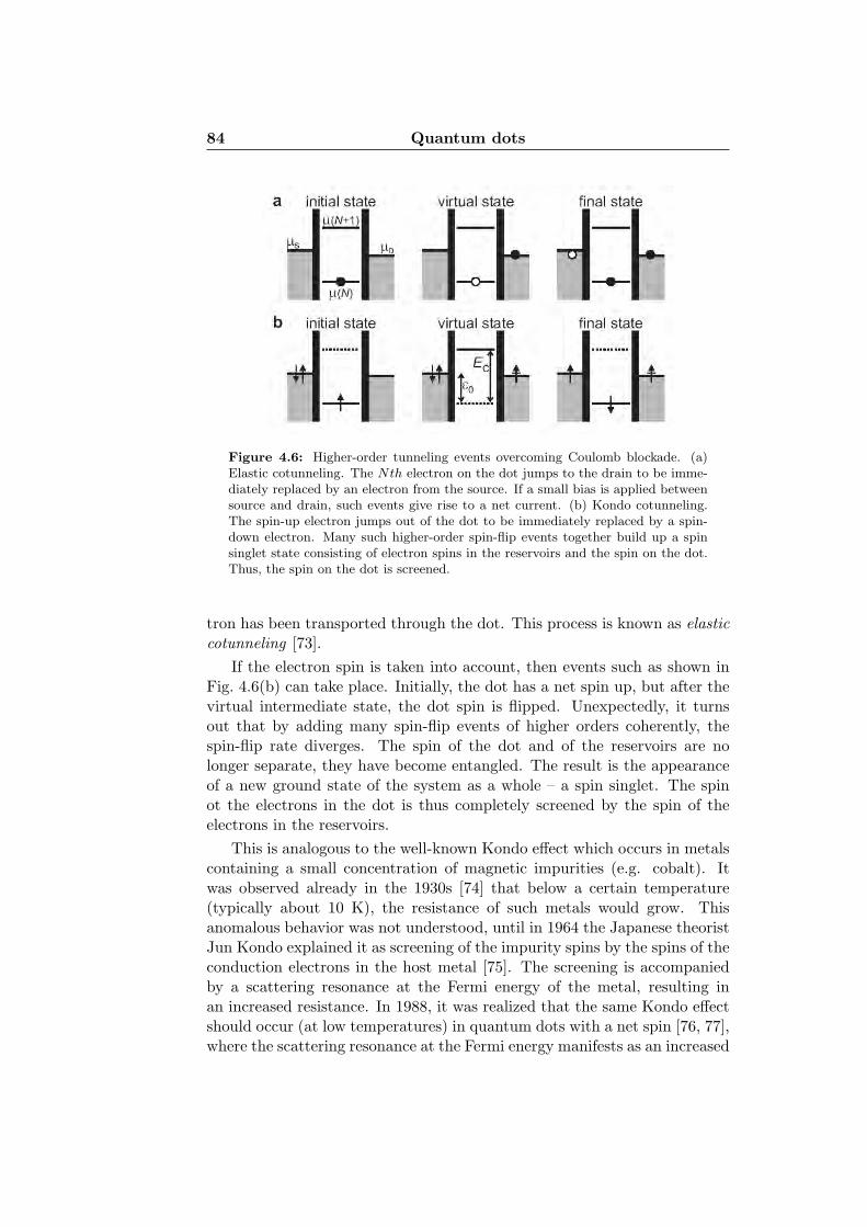
the near-surface region where the impinging molecular beams interact withthe hot substrate. This is the phase where the phenomena most relevant tothe MBE process take place. Atomic or molecular species get physisorbedor chemisorbed on the surface where they can undergo different processes(Fig. 1.2). Atoms can diffuse on a flat surface (a), where they can re-evaporate (b), meet other atoms to form two-dimensional clusters (c), reacha step where they can be incorporated (d), or further migrate along the stepedge (e) to be incorporated at a kink (f).
The MBE growth of III-V semiconductors uses the so called three tem-peratures method [1], in which the substrate is kept at an intermediate tem-perature between the evaporation temperature of the group III and groupV source materials. Group V species have a much higher vapor pressurethan group III atoms, therefore typical cell working temperatures are lowerfor group V evaporation (around 300C for As) than for group III species(around 1100C, 800C and 1000C, for Al, In, and Ga, respectively).
At the substrate temperature, the vapor pressure of group III species isnearly zero; this means that every atom of the III species that impinges onthe substrate is chemisorbed on its surface; in other words group III atomshave a unit sticking coefficient. The high vapor pressure of the group Vspecies favors, on the contrary, the re-evaporation of these species from thesample surface. Due to the higher group V species volatility with respectto group III, growth is usually performed with an V/III beam flux ratiomuch higher than one. This flux imbalance does not affect the one-to-onecrystal stoichiometry between III-V species. In fact, as shown by Foxon andJoyce [3, 4], in the case of homoepitaxial growth of GaAs, As atoms do notstick if Ga atoms are not available on the surface for bonding. So, in thecase of GaAs, the growth rate is driven by the rate of impinging Ga atomson the substrate.
Instruments and Techniques 9
The flux J of atoms evaporated from an effusion cell can be describedas [1]
J = 1.11× 10²² ×[
aP
d2√
MT
]cos θ mol cm−2 s−1 , (1.1)
where a is the aperture area of the effusion cell, d is the distance of theaperture to the sample, θ is the angle between the beam and the normal tosubstrate, M is the molecular weight of the beam species, T the temperatureof the source cell, and P is the vapor pressure of the beam; the vapor pressureis itself a function of the source cell temperature as
log P =A
T+ B log T + C , (1.2)
where A, B and C are material-dependent constants. For a growth rate ofabout 1 µm/h the typical fluxes are ∼ 1016 atoms cm−2 s−1 for group Velements and ∼ 1015 atoms cm−2 s−1 for group III.
In the case of alloys with mixed group III elements, such as InGaAsand InAlAs, the reactions with the group V elements are identical to thoseobserved in the growth of binary compounds, such as GaAs [3, 4]. Theonly difference is that the optimum growth temperature range is driven bythe less stable of the two group III atoms, i.e. by indium in the case ofInGaAs and InAlAs alloys. In fact, Turco et al. [5] observed that theincorporation of In in InAlAs alloys grown on GaAs substrates decreases forsamples grown at temperatures higher than 500C, while significant Ga orAl re-evaporation takes place only at higher temperatures (about 650C forGa, and about 750C for Al).
In the case of substrate temperatures below 500C a unit sticking coeffi-cient can be assumed for the growth of In-based alloys; the resulting growthrate and composition are simply derived from the two binary growth ratesthat form the alloy. For example if RInAs, and RGaAs are the growth ratesfor InAs and GaAs respectively, then the total growth rate of the alloy isRInGaAs = RInAs +RGaAs while the indium concentration x is the same asin the gas phase and is given by
x =RInAs
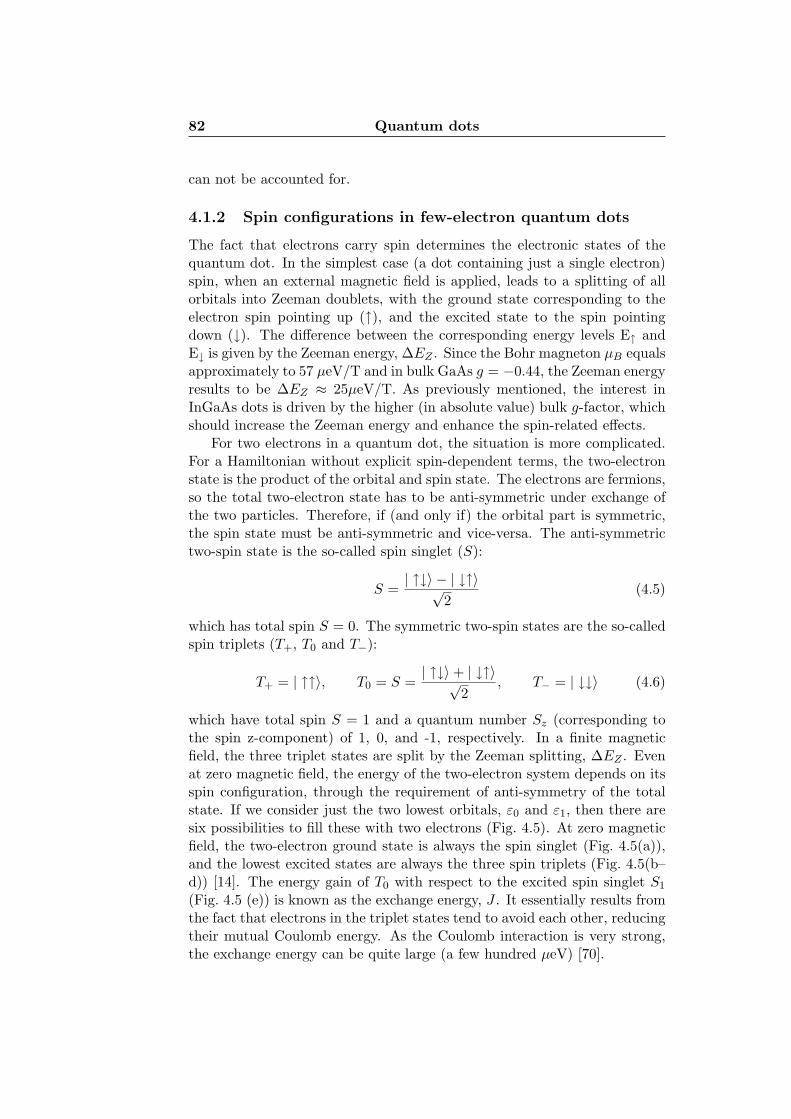
RInAs +RGaAs. (1.3)
1.1.3 Growth rate calibration
To grow ternary alloys as InxGa1−xAs and InxAl1−xAs with known indiumconcentration x, it is necessary to measure accurately, prior to growth, thethree growth rates RGaAs, RAlAs, and RInAs.
GaAs and AlAs
The growth rates of GaAs and AlAs are determined by the intensity os-cillations of the specular spot of the RHEED signal during the growth of
10 Molecular beam epitaxy
0 10 20 30 40 50
RH
EE
D i
nte
ns
ity
(A
rb.
Un
its
)
Time (s)
shutters openshutters closed
GaAs
AlAs
Figure 1.3: RHEED oscillations. In the left panel an actual measurement forGaAs and AlAs grown on GaAs (001). In the right panel a schematic view of therelationship between RHEED intensity and monolayer coverage θ.
a GaAs or AlAs film on a GaAs substrate [1]. This technique employs ahigh energy (up to 20 keV) electron beam, directed on the sample surfaceat grazing incidence (a few degrees); the diffraction pattern of the electronsis displayed on a fluorescent screen and acquired by a CCD. Thanks to thegrazing incidence and the limited mean free path of electrons in solids, theelectron beam is scattered only by the very first atomic layers, giving rise toa surface-sensitive diffraction pattern. Besides, the grazing geometry limitsthe interference of the RHEED electrons with the molecular beams, makingthe technique suitable for real-time analysis during growth.
During crystal growth the intensity of the zero order diffraction spot (thespecular spot) is recorded as a function of time. An example of such mea-surements is shown in the left panel of figure 1.3, where it can be noticedthat the intensity of the spot has an oscillatory behavior. This happensbecause a flat surface, present when a monolayer is complete, reflects opti-mally the electrons while in a condition in which a half-monolayer has beendeposited the electron beam gets partially scattered by the stepped surface.
As schematically shown in the right panel of figure 1.3, starting witha flat surface and proceeding with growth, the incident electron beam getspartially scattered by the islands steps of the growing monolayer, thus reduc-ing the reflected intensity. Scattering becomes maximum at half monolayercoverage, while as the new monolayer completes (one Ga or Al plus one Aslayer) the surface flattens again by coalescence of the islands, and the re-flected intensity recovers its value. A progressive dumping of the oscillationintensity is due to an increasing disorder of the growth front as the growthproceeds.
Instruments and Techniques 11
Thus, a period of RHEED oscillation corresponds to the growth of asingle monolayer. By measuring the time necessary to complete a certainnumber of oscillations one can calculate the growth rate in monolayer/s for afixed effusion cell temperature, and easily convert it to units of A/s knowingthe lattice parameter of GaAs or AlAs.
This calibration is performed almost daily, prior to sample growth, ona ad hoc substrate. The day-to-day variation of RGaAs and RAlAs, withconstant cell temperatures is ∼1%; the long term behavior of these rates, onthe other hand is fairly predictable, and is constant (within 1−2%) until thecell is almost empty, unless major changes to the cell environment happen(like refilling, etc.).
InAs
Unfortunately, InAs growth rates cannot be measured taking advantage ofRHEED oscillations. This is because it is very difficult to obtain goodquality, monolayer-flat InAs surfaces on any substrate, and it is virtuallyimpossible on GaAs ones. In fact the large lattice mismatch between InAsand GaAs (∼7.2%) favors the formations of 3D islands even after the firstone or two monolayers. However the relation ((1.3)) provides an alternativemethod to evaluate the InAs growth rate, by in-situ measuring the GaAsgrowth rate by RHEED oscillations, and the In concentration in a thickInGaAs layer by ex-situ X-ray diffraction measurements (see section 1.2.3).
The indium flux calibration is a time-consuming operation that involvesthe growth of several samples of InxGa1−xAs, and multiple X-ray diffractionmeasurements on each sample. For this reason, and knowing the relative sta-bility of the fluxes until the cells are almost empty, the In flux calibration isperformed only once every few months, after major maintenance operationsto the MBE chamber.
1.1.4 The MBE system at Laboratorio TASC
The MBE chamber installed at Laboratorio TASC INFM-CNR in Trieste ismainly dedicated to the growth of GaAs based heterostructures character-ized by a very high carrier mobility. Such a system requires some peculiarmodifications. Two 3000 l/s cryopumps replace the ion pumps, providing acleaner, higher-capacity pumping system. All-metal gate valves are mountedto eliminate outgassing from Viton seals. No group-II materials, such as Be,are used for p-doping, since they are known to drastically reduce carriermobility. High-capacity and duplicate cells are used to avoid cell refilling orrepairing for extended periods. Extensive degassing and bake out duration(three months at 200C) were carried out after the installation of the MBEsystem to increase the purity of the materials.
12 High resolution X-ray diffraction
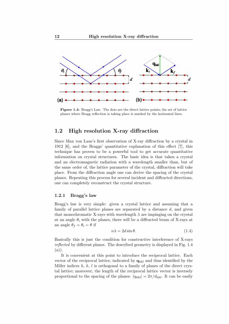
Figure 1.4: Bragg’s Law. The dots are the direct lattice points; the set of latticeplanes where Bragg reflection is taking place is marked by the horizontal lines.
1.2 High resolution X-ray diffraction
Since Max von Laue’s first observation of X-ray diffraction by a crystal in1912 [6], and the Braggs’ quantitative explanation of this effect [7], thistechnique has proven to be a powerful tool to get accurate quantitativeinformation on crystal structures. The basic idea is that taken a crystaland an electromagnetic radiation with a wavelength smaller than, but ofthe same order of, the lattice parameter of the crystal, diffraction will takeplace. From the diffraction angle one can derive the spacing of the crystalplanes. Repeating this process for several incident and diffracted directions,one can completely reconstruct the crystal structure.
1.2.1 Bragg’s law
Bragg’s law is very simple: given a crystal lattice and assuming that afamily of parallel lattice planes are separated by a distance d, and giventhat monochromatic X-rays with wavelength λ are impinging on the crystalat an angle θi with the planes, there will be a diffracted beam of X-rays atan angle θf = θi = θ if
nλ = 2d sin θ. (1.4)
Basically this is just the condition for constructive interference of X-raysreflected by different planes. The described geometry is displayed in Fig. 1.4(a)).
It is convenient at this point to introduce the reciprocal lattice. Eachvector of the reciprocal lattice, indicated by qhkl and thus identified by theMiller indices h, k, l is orthogonal to a family of planes of the direct crys-tal lattice; moreover, the length of the reciprocal lattice vector is inverselyproportional to the spacing of the planes: |qhkl| = 2π/dhkl. It can be easily
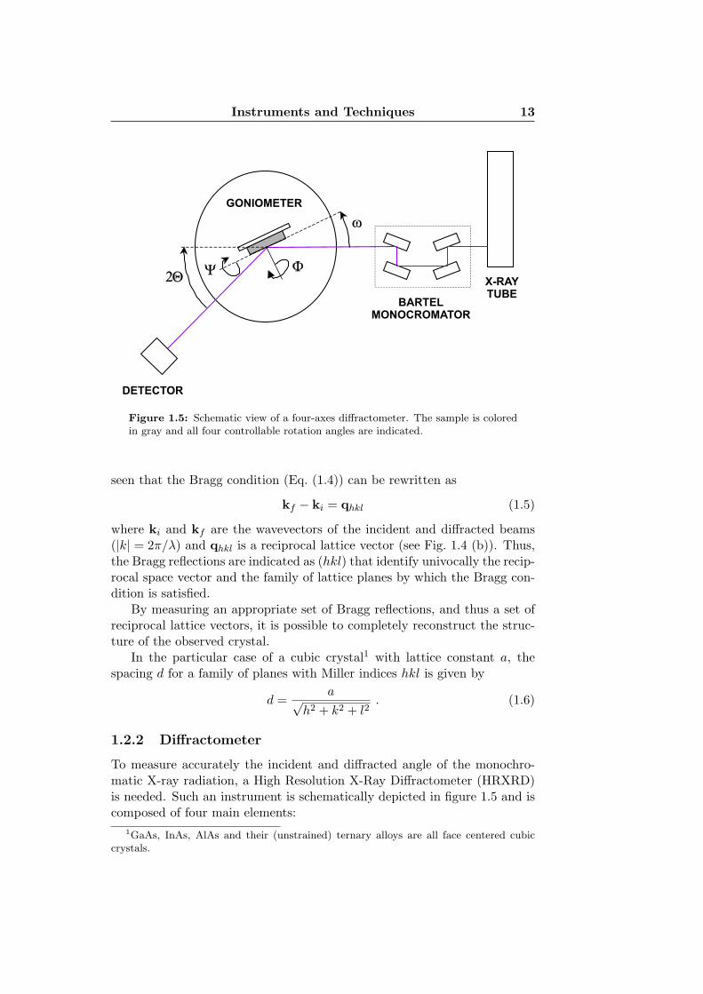
Instruments and Techniques 13
2Q
w
FY
DETECTOR
GONIOMETER
BARTEL
MONOCROMATOR
X-RAY
TUBE
Figure 1.5: Schematic view of a four-axes diffractometer. The sample is coloredin gray and all four controllable rotation angles are indicated.
seen that the Bragg condition (Eq. (1.4)) can be rewritten as
kf − ki = qhkl (1.5)
where ki and kf are the wavevectors of the incident and diffracted beams(|k| = 2π/λ) and qhkl is a reciprocal lattice vector (see Fig. 1.4 (b)). Thus,the Bragg reflections are indicated as (hkl) that identify univocally the recip-rocal space vector and the family of lattice planes by which the Bragg con-dition is satisfied.
By measuring an appropriate set of Bragg reflections, and thus a set ofreciprocal lattice vectors, it is possible to completely reconstruct the struc-ture of the observed crystal.
In the particular case of a cubic crystal1 with lattice constant a, thespacing d for a family of planes with Miller indices hkl is given by
d =a√
h2 + k2 + l2. (1.6)
1.2.2 Diffractometer
To measure accurately the incident and diffracted angle of the monochro-matic X-ray radiation, a High Resolution X-Ray Diffractometer (HRXRD)is needed. Such an instrument is schematically depicted in figure 1.5 and iscomposed of four main elements:
1GaAs, InAs, AlAs and their (unstrained) ternary alloys are all face centered cubiccrystals.
14 High resolution X-ray diffraction
• The X-ray tube. It generally consists of a metal anode hit by a beamof high energy (30-40 keV) electrons emitted by a nearby cathode; thecore level electrons of the anode’s atoms are excited and when theyrecombine they emit X-ray photons at a discrete set of wavelengths,characteristic of the anode’s element. In our setup a copper anodetube has been used.
• The monochromator selects only one of the emitted wavelengths. Forhigh resolution diffraction measurements the wavelength has to be veryprecisely selected. To accomplish this, the X-rays undergo multipleBragg reflections in appropriately chosen single crystals; this has alsothe appreciated side-effect of greatly reducing the angular divergenceof the outcoming beam. For our measurements we have always useda so-called Bartel monochromator, in which the beam undergoes fourtimes the 220 reflection in germanium single-crystals. This gives anuncertainty in the determination of the wavelength of less than onepart in 100,000 and an angular divergence of 12 arcsec.
• The goniometer is responsible for the measurements of the Bragg an-gles and the appropriate alignment of the crystal planes with respectto the incident beam. Four angles can be adjusted: 2θ is twice the dif-fraction angle while ω is the angle between the incident beam and thesurface sample. Since these two angles alone are needed to extract thelattice plane spacing, their setting and determination has to be as ac-curate as possible. In our instrument their resolution is 10−5 degrees.The other two angles, Ψ and Φ, necessary only to align the samplecrystal axes to the incident beam, are less important in determiningthe overall resolution of the measurements; in our diffractometer theyhave a resolution of 0.01 degree.
• The detector collects and counts the X-ray photons. According tothe resolution to be achieved it can be coupled to a receiving slitthat simply limits the acceptance angle of the detector or to anothergermanium monochromator (which increases the resolution, but onthe other hand reduces greatly the count rate, thus increasing theacquisition times).
The diffractometer employed to perform the measurements presented inthis thesis, and shown in figure 1.6, is a Phillips X’Pert-MRD using a Cu-Kα
radiation with a wavelength λ = 1.54056 A.
1.2.3 Strain and alloy composition in epilayers
In this thesis X-ray diffraction has been used both for indium flux cali-bration and for indium concentration and residual strain measurements in
Instruments and Techniques 15
Figure 1.6: The Phillips X’Pert-MRD High Resolution X-Ray Diffractometeremployed in this thesis.
InxGa1−xAs/InxAl1−xAs quantum wells grown on GaAs substrates. Thisgreatly simplifies the analysis of diffraction data since all indium containinglayers are grown epitaxially on GaAs 〈001〉, have the same crystal lattice(face-centered cubic), and have lattice constants of comparable size. Thisallows to measure the overlayer crystal structure by comparison to GaAs.Typically one only measures the difference ∆θ of the angle of the diffractionpeak of the overlayer with respect to the peak of the substrate, perform-ing a so called rocking curve or ω-2θ scan. A rocking curve consists in asimultaneous scan of the angles 2θ and ω so that one probes reciprocal lat-tice vectors of different length but same orientation. Before a rocking curvemeasurement the crystal plane of the substrate must be aligned with respectto the diffractometer setup, by maximizing the peak intensity of GaAs withrespect the two angles Ψ and Φ.
As pointed out by Hornstra and Bartels [8], the measured angular dif-ference ∆θM between epilayer and substrate can be different from the realdifference ∆θB due to tilting effects between the substrate and the overlayer.However, this tilt effect can be eliminated by measuring four rocking curvesafter successive 90 rotations of the sample around the Φ axis; the correctBragg angle difference is then
∆θB =∆θ0
M + ∆θ90M + ∆θ180
M + ∆θ270M
4. (1.7)
16 High resolution X-ray diffraction
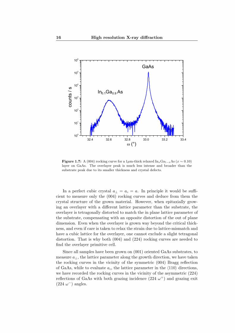
Figure 1.7: A (004) rocking curve for a 1µm-thick relaxed InxGa1−xAs (x ∼ 0.10)layer on GaAs. The overlayer peak is much less intense and broader than thesubstrate peak due to its smaller thickness and crystal defects.
In a perfect cubic crystal a⊥ = aq = a. In principle it would be suffi-cient to measure only the (004) rocking curves and deduce from them thecrystal structure of the grown material. However, when epitaxially grow-ing an overlayer with a different lattice parameter than the substrate, theoverlayer is tetragonally distorted to match the in plane lattice parameter ofthe substrate, compensating with an opposite distortion of the out of planedimension. Even when the overlayer is grown way beyond the critical thick-ness, and even if care is taken to relax the strain due to lattice-mismatch andhave a cubic lattice for the overlayer, one cannot exclude a slight tetragonaldistortion. That is why both (004) and (224) rocking curves are needed tofind the overlayer primitive cell.
Since all samples have been grown on (001) oriented GaAs substrates, tomeasure a⊥, the lattice parameter along the growth direction, we have takenthe rocking curves in the vicinity of the symmetric (004) Bragg reflectionof GaAs, while to evaluate aq, the lattice parameter in the 〈110〉 directions,we have recorded the rocking curves in the vicinity of the asymmetric (224)reflections of GaAs with both grazing incidence (224 ω+) and grazing exit(224 ω−) angles.
Instruments and Techniques 17
The [001] lattice parameter is then calculated as
a⊥ =λ
2 sin(θ(004)B + ∆θ
(004)B )
, (1.8)
while the 〈110〉 lattice parameter is
aq =
√√√√√ 8(2 sin(θ
(224)B +∆θ
(224)B )
λ
)2
−(
4a⊥
)2. (1.9)
In these expressions θ(004)B and θ
(224)B are the Bragg angles of GaAs for the
(004) and (224) reflections, and ∆θ(004)B and ∆θ
(224)B are the angular distances
of the overlayer peak with respect to the GaAs one. A typical (004) rockingcurve is plotted in figure 1.7.
To get the indium concentration x of the alloy layer knowing both the inplane and out of plane lattice parameters, one has to take into account thetetragonal distortion and rely on elasticity theory to derive the “unstrained”lattice parameter of the alloy [9]. Practically one has to self-consistentlysolve the following equation:
ε⊥(x) = −2C12(x)C11(x)
εq(x) , (1.10)
where ε⊥(x) = a⊥−a0(x)a0(x) and εq(x) = aq−a0(x)
a0(x) with a0(x), C11(x) and C12(x)are the lattice parameter of the unstrained unit cell and the stiffness con-stants of the layer with In concentration x respectively. These values areobtained by linear interpolation of the binary compounds values as statedby Vergard’s law and confirmed by recent literature [10].
1.3 Atomic force microscopy
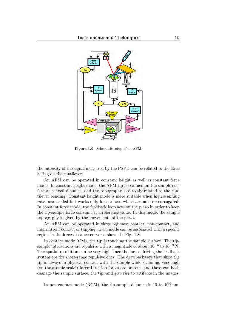
In 1986, Binnig, Quate, and Gerber invented a new type of microscope, theatomic force microscope (AFM), able to obtain high resolution images ofboth conductive and insulating samples. The AFM belongs to the familyof the scanning probe microscopes (SPMs). The idea behind all SPMs isvery simple: the sample to be investigated or the microscope probe (tip) ismounted onto a piezo-resistive crystal (piezo). The piezo is deformed withsub-nanometer accuracy in all three dimensions by applying voltages. Thevarious SPMs differ in the parameter used to detect the tip-sample distance.For the AFM the monitoring parameter is the force between tip and sample.
18 Atomic force microscopy
Figure 1.8: Typical force versus tip-sample distance curve. Indicated are theforce regimes of contact, non-contact, and intermittent-contact mode.
The main forces present between tip and sample arise from [11]: (i)electrostatic or Coulomb interactions; (ii) polarization forces; (iii) quantum-mechanical forces, which give rise to covalent bonding and repulsive ex-change interactions; (iv) capillary forces present when the AFM is operatingin a humid environment.
Capillary forces are always attractive with a magnitude of about 10−8 N.When the tip is far away from the sample, the interaction is an attractiveVan der Waals force. When the tip-sample distance becomes of the order ofthe interatomic distances in solids (a few Angstroms), repulsive forces startdominating and become extremely strong when the electronic clouds of theatoms of tip and sample start to overlap (see figure 1.8). The tip-sampleinteractions are usually described by a Lennard-Jones potential:
U(d) = 4ε
[(σ
d
)12−
(σ
d
)6]
, (1.11)
where d is the tip-sample distance, σ is the distance at which U(σ)=0, and-ε is the energy value in the equilibrium position deq=σ 6
√2. The derivative
of Eq. (1.11) represents, to a first approximation, the force between tip andsample (see Fig. 1.8).
1.3.1 AFM operation
All the experiments described in this thesis have been performed using a CPResearch, VEECO AFM system. The key elements of an AFM are showin Fig. 1.9. The AFM tip, fixed to a cantilever, is mounted on a carrierchip and approaches the sample using the Z-motor. When the tip interactswith the sample, the cantilever bends. This bending is measured by meansof a laser beam which is deflected by the back of the cantilever onto aPosition Sensitive PhotoDetector (PSPD). When the force is changing, thecantilever deflection changes, and the laser spot on the PSPD moves. Thus,
Instruments and Techniques 19
Figure 1.9: Schematic setup of an AFM.
the intensity of the signal measured by the PSPD can be related to the forceacting on the cantilever.
An AFM can be operated in constant height as well as constant forcemode. In constant height mode, the AFM tip is scanned on the sample sur-face at a fixed distance, and the topography is directly related to the can-tilever bending. Constant height mode is more suitable when high scanningrates are needed but works only for surfaces which are not too corrugated.In constant force mode, the feedback loop acts on the piezo in order to keepthe tip-sample force constant at a reference value. In this mode, the sampletopography is given by the movements of the piezo.
An AFM can be operated in three regimes: contact, non-contact, andintermittent contact or tapping. Each mode can be associated with a specificregion in the force-distance curve as shown in Fig. 1.8.
In contact mode (CM), the tip is touching the sample surface. The tip-sample interactions are repulsive with a magnitude of about 10−6 to 10−9 N.The spatial resolution can be very high since the forces driving the feedbacksystem are the short-range repulsive ones. The drawbacks are that since thetip is always in physical contact with the sample while scanning, very high(on the atomic scale!) lateral friction forces are present, and these can bothdamage the sample surface, the tip, and give rise to artifacts in the images.
In non-contact mode (NCM), the tip-sample distance is 10 to 100 nm.
20 Atomic force microscopy
Figure 1.10: Changes of the vibration amplitude of an AFM cantilever vibratingabove the sample surface in the case of (a) non-contact mode and (b) intermittentcontact mode.
The tip-sample force, due to van der Waals interactions, is attractive witha typical magnitude of the order of 10−9 to 10−12 N and positive derivative.Far away from the sample, the cantilever is vibrating at a frequency ωr justabove its resonance frequency ω0. As the tip is approaching the sample, theinteraction induces a decrease in the resonance frequency ωint according to
ωint =
√ω2
0 −1m· ∂F ts
∂r, (1.12)
where F ts is the tip-sample force. This induces a decrease of the amplitudeof the oscillation (see Fig. 1.10(a)) which is monitored by the feedback loopto control the tip-sample distance. In non-contact mode, the strength ofthe tip-sample interaction is 103 to 106 times lower than in contact mode;thus this operation mode is indicated to image very delicate samples such asorganic films. However, the spatial resolution that can be achieved is lowerthan in contact mode since non-contact AFM is based on long range vander Waals interactions.
The intermittent contact mode (ICM) is based on the same principles ofNCM, but in ICM the cantilever is vibrating at a frequency just below thenatural frequency of the cantilever. Thus, as the tip is brought closer to thesample, the vibration amplitude increases (see Fig. 1.10(b)) up to the pointwhere the tip touches the sample surface at the end of every oscillation. Thisinduces a reduction of the vibration amplitude to the set value. As in NCM,the vibration amplitude is used to control the tip-sample distance. In ICMthe spatial resolution is comparable with that of CM while the interactionstrength is intermediate between CM and NCM; moreover lateral frictionforces are virtually absent, allowing the imaging of delicate samples. Alltopographies shown in this theses are taken using ICM.
Instruments and Techniques 21
Figure 1.11: Layer sequence (on the top) and conduction band profiles (bottom)for two types of 2DEGs: on the left a Si MOSFET inversion layer and on the righta GaAs/AlGaAs modulation doped single heterostructure (from von Klitzing’sNobel lecture [12]).
1.4 Two dimensional electron gases
The transport experiments described in this thesis have as starting pointa two-dimensional electron gas (2DEG). This section describes the experi-mental realization of 2DEGs.
The first experimentally obtained 2DEG has been formed in the inver-sion layer of a silicon MOSFET2 (on the left side of Fig. 1.11) [13]; suc-cessively great success has been obtained in MBE-grown remotely dopedGaAs/AlGaAs single heterojunctions (on the right side of figure 1.11) andquantum wells (Fig. 1.13).
For Si inversion layers a bulk p-doped Si sample is taken, an insulatingoxide layer is grown on it and a metal layer is deposited on top of it. Applyinga positive voltage to the metal gate, the Si bands are bent so that at thesilicon-oxide interface the conduction band falls below the Fermi level, anda triangular potential well is formed (see left side of Fig. 1.11). Electronsare thus free to move in the two dimensions parallel to the surface, but areconfined in a narrow well perpendicular to the surface. While this type ofdevices has allowed pioneering studies on two-dimensional systems, the factthat the electrons are confined at the (far from perfect) silicon-oxide interface
2Metal-oxide-semiconductor field effect transistor.
22 Two dimensional electron gases
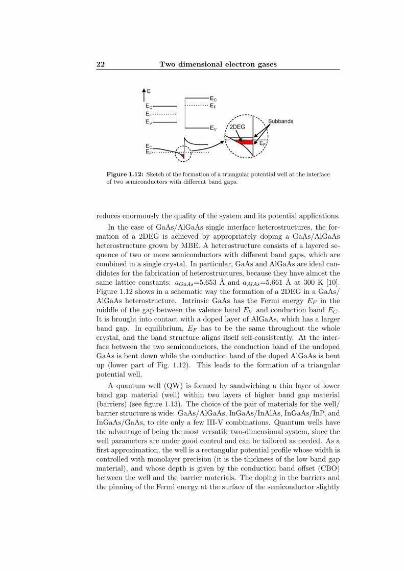
Figure 1.12: Sketch of the formation of a triangular potential well at the interfaceof two semiconductors with different band gaps.
reduces enormously the quality of the system and its potential applications.
In the case of GaAs/AlGaAs single interface heterostructures, the for-mation of a 2DEG is achieved by appropriately doping a GaAs/AlGaAsheterostructure grown by MBE. A heterostructure consists of a layered se-quence of two or more semiconductors with different band gaps, which arecombined in a single crystal. In particular, GaAs and AlGaAs are ideal can-didates for the fabrication of heterostructures, because they have almost thesame lattice constants: aGaAs=5.653 A and aAlAs=5.661 A at 300 K [10].Figure 1.12 shows in a schematic way the formation of a 2DEG in a GaAs/AlGaAs heterostructure. Intrinsic GaAs has the Fermi energy EF in themiddle of the gap between the valence band EV and conduction band EC .It is brought into contact with a doped layer of AlGaAs, which has a largerband gap. In equilibrium, EF has to be the same throughout the wholecrystal, and the band structure aligns itself self-consistently. At the inter-face between the two semiconductors, the conduction band of the undopedGaAs is bent down while the conduction band of the doped AlGaAs is bentup (lower part of Fig. 1.12). This leads to the formation of a triangularpotential well.
A quantum well (QW) is formed by sandwiching a thin layer of lowerband gap material (well) within two layers of higher band gap material(barriers) (see figure 1.13). The choice of the pair of materials for the well/barrier structure is wide: GaAs/AlGaAs, InGaAs/InAlAs, InGaAs/InP, andInGaAs/GaAs, to cite only a few III-V combinations. Quantum wells havethe advantage of being the most versatile two-dimensional system, since thewell parameters are under good control and can be tailored as needed. As afirst approximation, the well is a rectangular potential profile whose width iscontrolled with monolayer precision (it is the thickness of the low band gapmaterial), and whose depth is given by the conduction band offset (CBO)between the well and the barrier materials. The doping in the barriers andthe pinning of the Fermi energy at the surface of the semiconductor slightly
Instruments and Techniques 23
0 50 100 150 200
-100
-50
0
50
100
150
200
250
300
350
surface
Charge density
Fermi energy
Ec-
F (
meV
)
distance from surface (nm)
substrate
In0
.75G
a0
.25A
s c
ap
uniformely n-doped
In0.75
Al0.25
As barrier
uniformely n-doped
In0.75
Al0.25
As barrier
In0
.75G
a0
.25A
s Q
W
Conduction
Band
Figure 1.13: In0.75Ga0.25As/In0.75Al0.25As quantum well. The top cartoon isa sketch of the layer sequence starting from the surface (left) down toward thesubstrate(right). The bottom graph is the profile of the calculated conductionband minimum along the growth direction (black curve), and the carrier densityprofile (red line); the horizontal red line is the Fermi level.
distort the shape of the well as can be seen in figure 1.13; in this figure a self-consistent Poisson-Schrodinger calculation of the conduction band profileand the carrier density for one of the In0.75Ga0.25As samples characterizedin this thesis are shown.
1.5 Device fabrication
1.5.1 Optical lithography
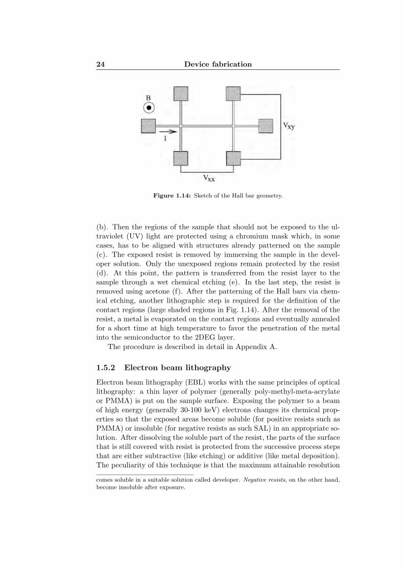
This section describes the procedure employed for the fabrication of semi-conductor heterostructure devices containing a 2DEG. These devices allowto perform transport measurements on the 2DEG itself.
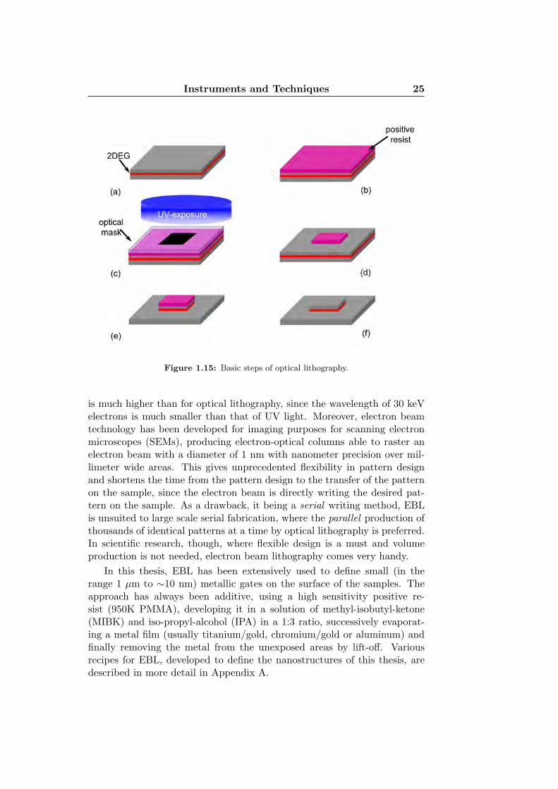
In the first fabrication step, properly designed structures are patternedon the sample. The geometry of the devices used in this thesis, commonlycalled Hall bar geometry, is shown in Fig. 1.14. This geometry is particu-larly indicated to study the mobility and carrier density of 2DEGs takingadvantage of the classical Hall effect. Hall bars are typically defined throughcommon optical lithography and a wet chemical etching process. Fig. 1.15shows the fundamental steps of device fabrication using optical lithography.First, the sample to be processed (a) is covered with a positive resist3 layer
3By positive resist we mean a polymer that after illumination with UV radiation be-
24 Device fabrication
Figure 1.14: Sketch of the Hall bar geometry.
(b). Then the regions of the sample that should not be exposed to the ul-traviolet (UV) light are protected using a chromium mask which, in somecases, has to be aligned with structures already patterned on the sample(c). The exposed resist is removed by immersing the sample in the devel-oper solution. Only the unexposed regions remain protected by the resist(d). At this point, the pattern is transferred from the resist layer to thesample through a wet chemical etching (e). In the last step, the resist isremoved using acetone (f). After the patterning of the Hall bars via chem-ical etching, another lithographic step is required for the definition of thecontact regions (large shaded regions in Fig. 1.14). After the removal of theresist, a metal is evaporated on the contact regions and eventually annealedfor a short time at high temperature to favor the penetration of the metalinto the semiconductor to the 2DEG layer.
The procedure is described in detail in Appendix A.
1.5.2 Electron beam lithography
Electron beam lithography (EBL) works with the same principles of opticallithography: a thin layer of polymer (generally poly-methyl-meta-acrylateor PMMA) is put on the sample surface. Exposing the polymer to a beamof high energy (generally 30-100 keV) electrons changes its chemical prop-erties so that the exposed areas become soluble (for positive resists such asPMMA) or insoluble (for negative resists as such SAL) in an appropriate so-lution. After dissolving the soluble part of the resist, the parts of the surfacethat is still covered with resist is protected from the successive process stepsthat are either subtractive (like etching) or additive (like metal deposition).The peculiarity of this technique is that the maximum attainable resolution
comes soluble in a suitable solution called developer. Negative resists, on the other hand,become insoluble after exposure.
Instruments and Techniques 25
Figure 1.15: Basic steps of optical lithography.
is much higher than for optical lithography, since the wavelength of 30 keVelectrons is much smaller than that of UV light. Moreover, electron beamtechnology has been developed for imaging purposes for scanning electronmicroscopes (SEMs), producing electron-optical columns able to raster anelectron beam with a diameter of 1 nm with nanometer precision over mil-limeter wide areas. This gives unprecedented flexibility in pattern designand shortens the time from the pattern design to the transfer of the patternon the sample, since the electron beam is directly writing the desired pat-tern on the sample. As a drawback, it being a serial writing method, EBLis unsuited to large scale serial fabrication, where the parallel production ofthousands of identical patterns at a time by optical lithography is preferred.In scientific research, though, where flexible design is a must and volumeproduction is not needed, electron beam lithography comes very handy.
In this thesis, EBL has been extensively used to define small (in therange 1 µm to ∼10 nm) metallic gates on the surface of the samples. Theapproach has always been additive, using a high sensitivity positive re-sist (950K PMMA), developing it in a solution of methyl-isobutyl-ketone(MIBK) and iso-propyl-alcohol (IPA) in a 1:3 ratio, successively evaporat-ing a metal film (usually titanium/gold, chromium/gold or aluminum) andfinally removing the metal from the unexposed areas by lift-off. Variousrecipes for EBL, developed to define the nanostructures of this thesis, aredescribed in more detail in Appendix A.
26 Transport measurements
1.6 Transport measurements
The study of the transport properties of the fabricated devices was per-formed in both a variable temperature 4He cryostat for measurements fromroom temperature down to 1.4 K and magnetic field up to 7 T and a 3Herefrigerator for temperatures down to 250 mK and magnetic fields up to12 T. The sample holders allow to perform measurements in a magneticfield either perpendicular or parallel to the sample.
The cooling of the sample in the 4He cryostat takes place by thermalexchange with cold 4He vapors that come from the liquid 4He reservoir of thecryostat. In this way it is possible to cool the sample down to 4.2 K. Furthercooling can be achieved by pumping the chamber in which the sample islocated down to a few mbar. In this way, the 4He coming from the reservoirundergoes an adiabatic expansion reducing its temperature to ∼1.4 K.
The 3He refrigerator (a Heliox system manufactured by Oxford Instru-ments) works with a three stage cooling strategy: first the whole insert isdipped into liquid helium, reaching 4.2 K temperature; then inside a vacuumchamber in the liquid helium bath a pumped 4He circuit cools a condensingplate down to ∼1.5 K. Here the 3He gas within its closed-loop circuit con-denses, accumulating in a pot in thermal contact with the sample. Once allthe 3He is liquefied, one reduces its vapor pressure through a sorb pump,lowering its temperature down to ∼250 mK.
Carrier density n and mobility µ of a 2DEG are measured in a four wiresetup, which is schematically described in Fig. 1.14. A current I is driventhrough the main channel of the Hall bar. At zero magnetic field (B=0),the potential drop Vxx induced by the current between two lateral contactsis measured. From Vxx it is possible to obtain the longitudinal resistivity,ρxx, of the 2DEG as
ρxx =Vxx
I· w
L, (1.13)
where w and L are the width and length of the Hall bar, respectively. Thedimensions of the typical Hall bars used in this thesis are w=60 µm andL=260 µm. If a magnetic field B perpendicular to the plane of the 2DEGis applied, the Lorentz force, ~I × ~B, induces a potential drop Vxy betweentwo transverse contacts (classical Hall effect). From the Drude model [14]it is than possible to obtain the following relations:
ρxx =1
enµ, (1.14)
n =B · Ie · Vxy
, (1.15)
where n is the carrier density of the 2DEG. Combining Eqs. (1.14) and (1.15)
Instruments and Techniques 27
with Eq. (1.13) results in the mobility µ of the 2DEG,
µ =Vxy
Vxx· L
B · w. (1.16)
The characterization of 2DEG mobility and carrier density is typically doneat T=1.4 K with a magnetic field B of 0.3 T. These measurements aretypically performed using a conventional four wire lock-in technique with anAC excitation current of 100 nA at a frequency of about 20 Hz.
Many of the low temperature measurements of this thesis have insteadbeen performed in a DC setup. For such measurements care must be takenin the measurement system to reduce the noise to a minimum. In particular,all signal wires pass through π-filters as they exit the cryostat and currentsand voltages to be measured are readily amplified by low-noise electronics.Both the amplifying electronics and the current and voltage sources arepowered by batteries and are driven by a computer program through anoptical fiber link to avoid any kind of external noise. The amplified signalsare then read by digital multimeters and acquired by software. A in-housedesigned additional filtering stage, composed of RC low-pass filters with acutoff frequency of ∼5 kHz, can be optionally added to the 300 mK stage ofthe cryostat to avoid electron gas heating by high frequency external noise.
28 Transport measurements
Chapter 2
InAlAs step-graded buffers
As already pointed out in sections 1.1.3 and 1.2, the growth of good qualityIn0.75Ga0.25As quantum wells is made very difficult by the absence of suitablesubstrates. One of our goals was to grow high electron mobility 2DEGs invirtually unstrained In0.75Ga0.25As QWs. To reach this result we had todevelop a virtual substrate, lattice-matched with In0.75Ga0.25As, bearing nocrystal defects, and grown on a commercially available material.
This chapter describes the properties of the InxAl1−xAs graded buffersthat we have optimized to accommodate our In0.75Ga0.25As QWs on GaAssubstrates. Section 2.1 reviews briefly the main problems encountered whentrying to perform lattice-mismatched growths, particularly focusing on III-Vsemiconductor systems. In Sec. 2.2 we describe the structural properties ofour InxAl1−xAs buffers analyzed by cross-sectional Transmission ElectronMicroscopy (TEM), X-Ray Diffraction (XRD) and Atomic Force Microscopy(AFM), while Sec. 2.3 shows how different buffer designs influence the lowtemperature transport characteristics of the 2DEG.
Part of the results presented in Sec. 2.2 and 2.3 have been published inRef. [15].
2.1 Lattice-mismatched growth
Apart from a few lucky exceptions, crystals of different semiconductors havedifferent lattice parameters or even different crystal structures. This makesit very difficult to grow heterostructures without the formation of crystaldefects. The most famous exception is that of GaAs, AlAs and their alloys.In fact not only both GaAs and AlAs crystals have a zincblende structure,but their lattice parameters differ so little that virtually any thickness of anyalloy of these binaries can be grown without having to worry about strainbuildup. Moreover, the band gaps of GaAs and AlAs are very different, sothat conduction band engineering can be easily done in AlGaAs/GaAs sys-tems. GaAs/AlGaAs multilayers have been used to fabricate (by a variety
30 Lattice-mismatched growth
Figure 2.1: Band gaps and lattice parameters of most binary semiconductors.GaAs, AlAs, InAs and their ternary alloys are brightly colored (re-elaboratedfrom [16]).
of growth techniques) extremely high mobility 2DEGs in modulation dopedsingle heterointerfaces [12], high mobility 2-Dimensional Hole Gases [17],2DEGs in almost arbitrarily shaped quantum wells, coupled 2DEGs in mul-tiple quantum wells, very high quality superlattices, and so on.
As can be seen in Fig. 2.1, the situation for InAs (and thus InxGa1−xAsalloys) is not as good: the lattice mismatch between InAs and the mostcommon III-V commercial substrate, GaAs, is huge (almost 7%), and withInP (other commercially available substrate) it is more than 3%. The onlypossible lattice-matched growth of an InxGa1−xAs alloy is with x = 0.53 onInP. This was not a suitable choice in our case for two reasons: first, ourtarget was x & 0.75, so strain buildup would have been a problem anyhow;second, phosphorus is a contaminant for high mobility 2DEGs in GaAs/AlGaAs, so InP can not be used as substrate in our MBE chamber.
Thus the only choice has been using GaAs as a substrate, and find a wayto relax the strain to grow In0.75Ga0.25As layer with a low defect density inthe active region of the structure.
2.1.1 Heteroepitaxy
Whenever growing an epilayer with a different lattice parameter than thesubstrate, strain will build up in the epilayer.
This strain can be either compressive, when the epilayer has a largerlattice parameter than the substrate (as is he case for InxGa1−xAs grown on
InAlAs step-graded buffers 31
Figure 2.2: Growth of a mismatched layer (red) on a substrate (blue) beyond thecritical thickness Tc. In (a) a representation of the “bulk” fully relaxed materials;(b)-(e) are the various phases of growth. Below the cartoons are shown the graphsof elastic energy per unit area versus epilayer thickness. The horizontal green linerepresents the critical energy for dislocation formation.
GaAs), or tensile, in the opposite case. In both cases the first atomic layers ofthe growing film tend to have the in-plane lattice parameter matched to thatof the substrate, and to expand or compress the out of plane lattice parame-ter to accommodate the misfit (the so called pseudomorphic growth). This,however, has an energy cost payed in elastic energy accumulation within thecrystal. When this elastic energy exceeds the energy cost of a crystal defect,the defect becomes energetically favorable and tends to form throughout theinterface between the epilayer and the substrate. This process is depictedin Fig. 2.2. The thickness at which defects start forming is called criti-cal thickness. There exist several equilibrium models to predict the criticalthickness of a strained layer, but MBE growth is far from equilibrium, andcritical thickness calculations have to rely on growth specific parameters (seeSec. 2.2).
The growth of an epilayer beyond the critical thickness, with the forma-tion of crystal defects that lead to the relaxation of the epilayer, is referredto as metamorphic.
The most common crystal defect forming to release the built up strainis a misfit dislocation (MD), depicted in Fig. 2.3(a): a whole row of crystalsites, lying parallel to the growth plane, is missing. This kind of defect canmove (glide) sideways in a direction perpendicular to both its own and thegrowth direction: such a direction is parallel to the surface, and thus thedislocation can not go deeper or move towards the surface; it is confinedat the depth at which it is formed. Another defect commonly associatedto strain relaxation is the so-called threading dislocation (TD), which is aMD which forms on a plane that is not the growth plane [19]. Figure 2.3(b)
32 Lattice-mismatched growth
Figure 2.3: Dislocations. (a) A misfit dislocation in a cubic lattice: the disloca-tion is highlighted in red and runs perpendicular to the page. Modified from [18].(b) A threading dislocation: the TD (drawn in red) originates from a MD (greenline) lying in the (001) plane and runs all the way to the free surface. Modifiedfrom [19].
schematically represents a TD running through a strained layer grown in the[001] direction; in this example the TD, running along the [011] direction,originates at the interface between the substrate and the strained layer at theend of a normal MD aligned along [110]. This kind of dislocations is to avoid,since they propagate all the way to the surface, and are detrimental for mostsemiconductor applications: they are sources of scattering for electrons andholes, non radiative recombination centers for optics, etc. This is true alsofor MDs, but the fact that they form at the interface between the substrateand the grown layer allows to keep them at a safe distance from the activelayer, thus reducing their potential harm.
As can be seen in Fig. 2.4, for a given thickness of the strained film theformation of dislocations is a function of the lattice mismatch; in practicethe slope of the line of the graphs of Fig. 2.2 gets steeper as the lattice
Figure 2.4: A qualitative plot of lattice energy stored at a heterointerface as afunction of lattice mismatch for a given epilayer thickness [20]; ε0 is the criticalmismatch: below this value of mismatch the epilayer will have no dislocations,above it will.
InAlAs step-graded buffers 33
Figure 2.5: A representative AFM topography of one of the In0.75Ga0.25As/In0.75Al0.25As samples (HM617), showing the characteristic cross-hatch pattern ofsurface roughness. The crystallographic directions that form the perpendicularnetwork of corrugations are indicated in the image. The image size is 15×15 µm2,while the vertical scale is 10 nm.
mismatch increases, thus reducing the critical thickness. This means that inorder to grow dislocation-free lattice mismatched layers there are only twostrategies:
• for small lattice mismatch: to grow pseudomorphic strained layersbelow the critical thickness (solution adopted for the devices of Chap-ter 4, with low indium content InxGa1−xAs);
• for large lattice mismatch: to grow first a buffer layer where strainrelaxation through MD formation takes place, i.e. to obtain a virtualsubstrate lattice-matched to InxGa1−xAs. The design and optimiza-tion of this buffer layer is the main matter of this chapter.
The surface of a metamorphic layer always shows a big roughness. Thisroughness typically is organized in a cross-hatch pattern (see Fig. 2.5) andhas root mean square (RMS) values from few nm to hundreds of nm, de-pending on the materials involved in the growth, the growth techniquesand growth conditions. Such cross-hatch patterns have been observed onSi1−xGex/Si [21], on InxGa1−xAs/GaAs [22, 23], and on InxGa1−xAs/InP[24]. Even though there have been many attempts to explain the formationof this roughness, there is no general agreement on the exact dynamics. Thetwo mainly proposed mechanisms are:
1. dislocation formation and glide on 111 planes and lateral mass trans-port to eliminate the surface steps [25];
2. locally enhanced or suppressed growth rate due to the nonconstantstrain field generated by dislocation bunching [22].
34 Structural properties
Our results reported in chapter 3 seem to confirm the second mechanism,but no detailed analysis of this problem has been carried out in this thesis.
2.1.2 Previous results for the growth of InGaAs QWs
Several research studies have been carried out to understand the mechanismsof strain relaxation in InxGa1−xAs or InxAl1−xAs layers in cases where alattice mismatch to the substrate exists [26, 27]. It was demonstrated thata defect-free region with an arbitrary indium concentration can be obtainedboth on GaAs and InP substrates by inserting a step- or linear-graded bufferlayer (BL) with increasing In composition in order to smoothly adapt thelattice constant of the substrate to the one of the topmost layer. Thisapproach enables to relax the strain and to bury the resulting dislocationsaway from the topmost defect-free epitaxial layers [28]. The key factors toreach this goal appear to be the low temperature growth of the BL [29], andthe insertion of a AlGaAs/GaAs superlattice between the GaAs substrateand the BL [30].
More recently, BLs were used to grow, on GaAs substrates, almost un-strained InxGa1−xAs QWs, (with x ≥ 0.7) containing a 2DEG with anelectron mobility higher than 20 m2/(Vs) [31, 32, 33]. In these cases the BLindium concentration was at the most equal to that of the QW. On the otherhand, increasing the indium concentration of the buffer up to values greaterthan the target concentration of the active layers has already proven to bebeneficial in InAlAs/InGaAs metamorphic QWs, but with much smaller Incontent (x = 0.33) [34], and in the growth of unstrained Zn0.75Cd0.25Selayers on In0.33Ga0.67As/GaAs buffers [35].
2.2 Structural properties
To obtain defect free active regions of InxGa1−xAs, we have grown step-graded InxAl1−xAs BLs with increasing indium concentration x on GaAs(001) wafers.
The growth procedure, schematically represented in figure 2.6, can bedivided in three phases characterized by different growth temperatures:
• Substrate preparation. The growth starts with an epiready GaAs(001) wafer degassed at 580C to remove the surface oxide. Thena 200 nm thick undoped GaAs layer followed by a 20 period GaAs/Al0.33Ga0.67As (8 nm/2 nm) superlattice and a second 200 nm un-doped GaAs layer are grown at 600C. These three layers have severalpurposes: to reduce the wafer roughness, the diffusion of interfaceimpurities in the grown layer, and to reduce the risk of threadingdislocation formation during the subsequent phase, as pointed out in
InAlAs step-graded buffers 35
Figure 2.6: The growth sequence of the InxGa1−xAs/InxAl1−xAs samples. In themiddle, a schematic view of the three parts of the growth. Each part is expandedon the sides. On the left is the buffer layer composition: the vertical axis representsthe distance from the top of the interfacial layer, and the horizontal axis is theindium concentration x.
Ref. [30]. They are grown at this temperature since it is the optimalgrowth temperature to obtain high quality GaAs.
• Buffer growth. The substrate temperature is decreased to 330C andthe InxAl1−xAs buffer is grown in 50 nm steps with increasing indiumconcentration, starting from In0.15Al0.85As. The increase in x betweeneach step is not constant throughout the buffer, but is ∼0.035 up to∼60% and then it is decreased to ∼0.025 up to the end of the buffer.The In concentration is varied by increasing the In cell temperaturewhile maintaining the Ga flux constant; there is no growth interruptionbetween the steps, so that the interface is not abrupt, since the increaseof the In cell temperature takes several seconds.
• Active layer. The substrate temperature is increased to 500C. Typi-cally this layer consists of a lower 50-100 nm thick In0.75Al0.25As bar-rier, a 10-30 nm thick In0.75Ga0.25As quantum well, an upper 130 nmthick In0.75Al0.25As barrier covered by a 5-10 nm thick In0.75Ga0.25Ascap layer. This capping layer is necessary to avoid extensive oxida-tion of the In0.75Al0.25As upper barrier. The details of the active layerare slightly different from sample to sample and will be described asneeded.
36 Structural properties
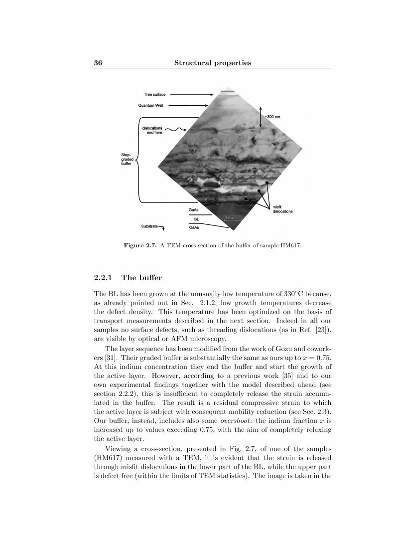
Figure 2.7: A TEM cross-section of the buffer of sample HM617.
2.2.1 The buffer
The BL has been grown at the unusually low temperature of 330C because,as already pointed out in Sec. 2.1.2, low growth temperatures decreasethe defect density. This temperature has been optimized on the basis oftransport measurements described in the next section. Indeed in all oursamples no surface defects, such as threading dislocations (as in Ref. [23]),are visible by optical or AFM microscopy.
The layer sequence has been modified from the work of Gozu and cowork-ers [31]. Their graded buffer is substantially the same as ours up to x = 0.75.At this indium concentration they end the buffer and start the growth ofthe active layer. However, according to a previous work [35] and to ourown experimental findings together with the model described ahead (seesection 2.2.2), this is insufficient to completely release the strain accumu-lated in the buffer. The result is a residual compressive strain to whichthe active layer is subject with consequent mobility reduction (see Sec. 2.3).Our buffer, instead, includes also some overshoot : the indium fraction x isincreased up to values exceeding 0.75, with the aim of completely relaxingthe active layer.
Viewing a cross-section, presented in Fig. 2.7, of one of the samples(HM617) measured with a TEM, it is evident that the strain is releasedthrough misfit dislocations in the lower part of the BL, while the upper partis defect free (within the limits of TEM statistics). The image is taken in the
InAlAs step-graded buffers 37
Figure 2.8: A TEM plan-view of the end of the MD network taken using the(004) reflection on HM617.
[110] direction, and shows a complicated network of dislocations extendingfrom the beginning of the BL up to roughly 450 nm from the surface. Similarimages taken in the [110] direction show that the last dislocations formfurther away to the surface, at a distance of ∼550 nm.
Figure 2.8 is a plan view image of the sample taken using the (004)reflection. Here the layer of dislocations closer to the surface is visible. Thisspecimen has been thinned down to electron transparency by a Xe+ ionbeam forming an angle of 4 with respect to the (001) plane. The result isa specimen of varying thickness with the thinnest parts closer to the surfaceof the sample while the thickest parts arrive in the BL. This is schematicallyrepresented in the drawing on the left. In the lower part of the image anetwork of MD is clearly visible, while in the upper part there are no visibledislocations. The contrast in the upper part of the image might be due tosome strain or indium concentration modulation.
2.2.2 Strain relief model
To analyze the strain relief in the buffer and compare it to the experimentalTEM and XRD results (presented in the next section), we have employedan isotropic model proposed by Romanato et al. [28].
This model assumes that, in a mismatched growth with given misfitprofile f(t)1, the density of misfit dislocations n(t) that relax the strain and
1Assuming the validity of Vergard’s law (confirmed for InxAl1−xAs by Ref. [10]), themisfit is linearly related to the In concentration. In fact if aA and aI are the lattice para-meters of AlAs and InAs, and a(x(t)) is the unstrained lattice parameter of InxAl1−xAswith a In concentration x(t) at the height t: a(x(t)) = x(t)aI + [(1 − x(t)]aA. Thenf(t) = (a(x(t))− a(x(t0)))/a(x(t0)), that is linear with x for a given t0.
38 Structural properties
the residual perpendicular strain ε⊥(t) are given by the following equations:
n(t) = 1beff
df(t)dt
ε⊥(t) = 0
for 0 < t < t0
n(t) = 0ε⊥(t) = 2C12
C11[f(t)− f(t0)]
for t0 < t < T
(2.1)
In Eq. (2.1) t is the distance from the substrate/buffer interface, T isthe total growth thickness, t0 is the thickness below which the layer is strainfree and the misfit dislocations are confined, beff is the misfit componentof the Burgers vector, and C11 and C12 are the elastic stiffness constants ofthe material.
The main assumption of this model is that the only mechanism to relaxthe strain is the formation of misfit dislocations; to be valid, any othermechanism has to be negligible. This is indeed reasonable since: (a) bordereffects play no role: the thickness of the film (∼ 1 µm) is much smaller thanthe area of the samples (∼ 1 cm); (b) there is no significant tilt of the epilayerwith respect to the substrate, as noted during the XRD measurements;(c) no other kind of dislocations, apart from MD, appears to form in thesamples. The second assumption is that the grown buffer, underneath thelast dislocation layer at a thickness t0, is completely relaxed, i.e. the misfitdislocations have a perfect efficiency in relaxing the built up strain.
I want to point out that if this model is accurate, the only way to changethe in-plane lattice parameter on top of the buffer, and match it to that ofthe active layer, is to form additional MDs deep in the buffer, raising thevalue of t0. Increasing the strain of the upper part of the buffer, withoutforming additional dislocations, has simply no effect on the in-plane latticeparameter.
One thing to note in Eq. (2.1) is that the density of misfit dislocationsn(t) is proportional to the misfit gradient df
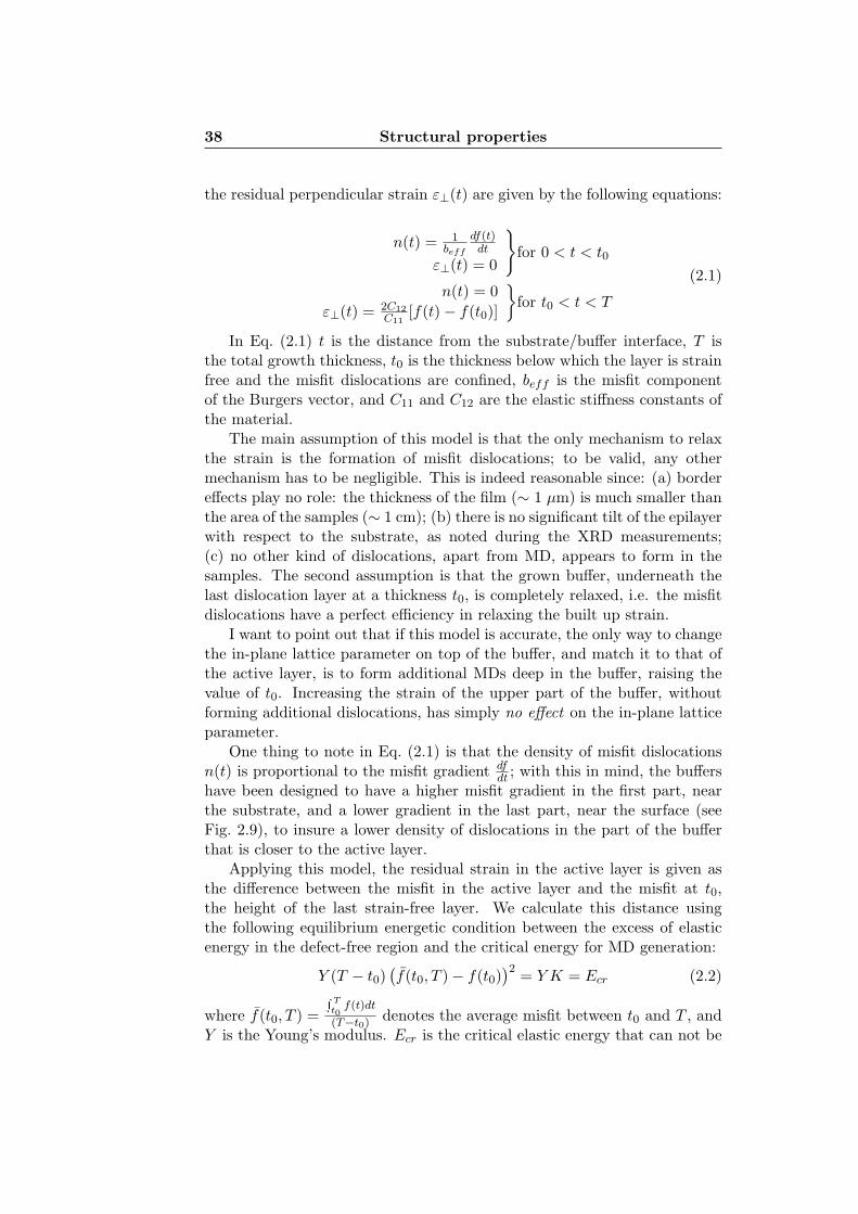
dt ; with this in mind, the buffershave been designed to have a higher misfit gradient in the first part, nearthe substrate, and a lower gradient in the last part, near the surface (seeFig. 2.9), to insure a lower density of dislocations in the part of the bufferthat is closer to the active layer.
Applying this model, the residual strain in the active layer is given asthe difference between the misfit in the active layer and the misfit at t0,the height of the last strain-free layer. We calculate this distance usingthe following equilibrium energetic condition between the excess of elasticenergy in the defect-free region and the critical energy for MD generation:
Y (T − t0)(f(t0, T )− f(t0)
)2 = Y K = Ecr (2.2)
where f(t0, T ) =R T
t0f(t)dt
(T−t0) denotes the average misfit between t0 and T , andY is the Young’s modulus. Ecr is the critical elastic energy that can not be
InAlAs step-graded buffers 39
Figure 2.9: Concentration profile versus thickness for the buffer and the activelayer. The average misfit gradient is calculated from the concentration for the firstpart of the buffer (red) and for the second one (blue).
exceeded without the nucleation of new misfit dislocations, and K = (3.7±0.7)× 10−3 nm is a phenomenological constant determined for InxGa1−xAslayers grown on GaAs in the concentration range 0.035 to 0.15 by Drigo etal. [36].
2.2.3 XRD measurements
To quantify the residual strain on the active layer we have performed HighResolution XRD measurements in a series of samples with different bufferdesigns. The four samples measured have the same structure, except for thefinal indium concentration xf at which the InxAl1−xAs buffer is stopped.The samples (see table 2.1) have nominal xf of 0.75 (sample A), 0.80 (sampleB), 0.85 (sample C), and 0.90 (sample D).
The first sample has thus the same structure of previous BLs (like thoseof Gozu and coworkers [31]), while in the others an overshoot is present. Thisis intended, as previously mentioned, to increase the stress in the buffer soto induce the formation of additional MDs to increase the in-plane latticeparameter at the top of the buffer. The key point is to induce the MDformation deep in the buffer, as far away as possible from the active layeritself. At the end of growth of this overshooting buffer, the top part of the BLis still strained, but has the same in-plane lattice parameter of the x = 0.75active layer. In this way one has at his disposal a virtual substrate thatis lattice-matched with In0.75Ga0.25As, and thus the possibility of growingan active layer of arbitrary thickness, without any constraints due to strainbuildup. The four samples were intended to accurately tune this overshootand compare the results with the quantitative model described in Sec. 2.2.2.
40 Structural properties
Figure 2.10: (004) rocking curves for the four samples described in table 2.1. Thecurves are shifted for clarity. The gray and yellow dotted lines are a guide to theeye to follow the peaks due to the InxAl1−xAs with x ∼ 0.60 and the In0.75Al0.25Asactive layer, respectively.
Sample xnomf xmeas
f xmeas ∆x ε⊥ εMOD⊥ T − t0
number name (%) (%) (%) (%) (×10−4) (×10−4) (nm)
HM1065 A 75 72±1 72±1 0 37±6 40 350HM1071 B 80 76±1 72±1 4±1 19±6 26 450HM1064 C 85 80±1 72±1 8±1 3±5 13 480HM1072 D 90 86±1 71±1 15±1 -14±9 -8 510
Table 2.1: Results of XRD on samples with different overshoot. The columnsshow the sample number, the short name of the sample, the nominal (nom) andmeasured (meas) value of xf (the final In concentration of the buffer), the mea-sured concentration of the active layer xmeas (which nominally was always 0.75),the difference ∆x = xmeas
f − xmeas, and the out of plane residual strain of theactive layer. The last two columns are the values of the residual strain in theactive layer and the depth of the last dislocation layer estimated with the modeldescribed in Sec. 2.2.2.
InAlAs step-graded buffers 41
The four samples were analyzed performing rocking curve measurementsfor both the symmetric (004) and the asymmetric (224) reflections. Aspointed out in Sec. 1.2.3, from these measurements both the residual strainand the indium concentration can be deduced. In the case of the BLs theanalysis is complicated by the fact that broad structures and multiple peaksare present in the rocking curves. Careful comparison of the spectra with thenominal growth structure, however, allows to extract the desired parameters.
The (004) rocking curves of the four samples are shown in figure 2.10.The buffer gives rise to a broad background with several peaks. The peakaround 31.5 is due to the layers with indium concentration close to 0.60 (seeFig. 2.9), and has a constant distance to the substrate peak. This means thatthe degree of relaxation of that layer is constant in the four samples. Thesmaller peak farthest from the GaAs substrate is the contribution of the lastlayer of the buffer, with xf indium concentration, that is obviously changingposition from sample to sample. Between these two, there is another peakwhich is decreasing its distance from GaAs peak with increasing xf . Thispeak is due to the active layer, composed mainly of In0.75Al0.25As withsmaller layers of In0.75Ga0.25As. The residual strain of the active layersshown in table 2.1 have been determined by fitting these peaks with gaussiancurves on both (004) and (224) scans (not shown).
The results of the fits are shown in Fig. 2.11, compared to the valuescalculated with the model described in the previous section, and in Table 2.1.The data show that it is possible to fine tune the residual strain on the activelayer through the introduction of an overshoot in the indium concentrationof the buffer. This allows to change the strain from compressive to slightlytensile passing through virtually unstrained samples.
Comparing the data with the model a good agreement is found, eventhough the constant K used in the calculation was derived from a verydifferent indium concentration range. This permits to use the model toestimate other characteristics of the samples. In fact, from the calculation,one can extract also the depth T − t0 at which the last dislocations arevisible, which is reported in the last column of Table 2.1. The calculatedT − t0 of sample C can be compared to the TEM observations on sampleHM617 shown before (since the two samples are nominally identical), andare found in good agreement. In fact the TEM observed distance of thelast dislocation layer to the surface is 450±50nm for the [110] images and550±50 for the [110] images2, to be compared with the figure of 480 nmresulting from the calculation.
2The anisotropy of MD formation along the two 〈110〉 directions is a well known prop-erty of III-V materials [37, 38, 39] and is not taken into account by the described model,which deals with averages of both types of MD, and considers t0 the average position (inthe two crystallographic directions) of the last MD layer.
42 Structural properties
Figure 2.11: Measured residual strains on the active layer compared with thecalculated ones.
2.2.4 Surface and interfaces
As previously mentioned, the surface of the samples shows a distinct cross-hatch pattern (CHP) of roughness which is observable with an AFM. Doesthis surface roughness give us some information on the interface roughnessbetween QW and barriers in the active layer? The answer, as we will see, isyes.
We have grown several samples interrupting the growth at different levelsof the active layer: all the samples are identical up to the end of the bufferlayer, which is the same as previously described for the samples measured byTEM and XRD. Above the last step of the buffer layer, with nominal 85% Incontent, we have grown In0.75Al0.25As layers of different thicknesses, cappedby a thin (5 nm) layer of In0.75Ga0.25As. The thickness of the In0.75Al0.25Aslayer for each of the samples is reported in Table 2.2. In what follows I willrefer to this top In0.75Al0.25As layer as “top layer” or TL.
AFM topographies have been recorded with image sizes of 5, 15, and30 µm. The acquired data have been flattened with a consistent protocol toremove long wavelength modulations that are artifacts due to AFM scannernonlinearities. Figure 2.12 reports 30×30 µm2 topographies of the samples.Panels (a) through (g) refer to the samples whose TL thickness is indicatedin table 2.2. Figure 2.13 is a plot of the RMS roughness of the samples ver-sus TL thickness. The TL of sample HM1292 (panel (f)) consists of the fullquantum well structure employed for low temperature transport measure-ments: 50 nm thick In0.75Al0.25As lower barrier, 30 nm thick In0.75Ga0.25AsQW and 120 nm thick In0.75Al0.25As upper barrier ended by the 5 nm thickIn0.75Ga0.25As capping. The graph shows also the roughness of other QW
aThis sample consists of the full QW structure; see text for details.
Table 2.2: Sample numbers, top layer (TL) thickness and RMS roughness of theAFM topographies shown in Fig. 2.12
Figure 2.12: 30×30 µm2 AFM topographies of the samples described in table 2.2.The blue arrow indicates the [110] direction in each image.
Figure 2.13: RMS roughnesses versus top layer thickness for the samples listedin table 2.2.
44 Transport measurements
Figure 2.14: Electron mobility µ (black symbols) and charge density n (redsymbols) versus buffer growth temperature.
samples (HM1327, HM1200, and HM889) which, as HM1292, have 200 nmtotal thickness above the buffer.
From this data it is evident that the roughness is nearly independentfrom the thickness grown above the buffer layer, and that the roughnessmeasured at the surface of a QW sample is approximately the same as thatof the interfaces between the QW and the barriers. This information willbe of particular value in the discussion of chapter 3.
2.3 Transport measurements
Our interest is, however, focused on the low temperature transport prop-erties of the 2DEG formed in the In0.75Ga0.25As QWs. Even though nointentional doping is introduced in the growth, the QWs are intrinsicallyn-type. This has already been shown by our group to be due to deep donorimpurities in the In0.75Al0.25As layers [40]. The energy of these deep donorimpurities is 120-170 meV below the conduction band edge of In0.75Al0.25As,and thus is within the conduction band discontinuity of the In0.75Al0.25As/In0.75Ga0.25As junction, making it easy to populate the In0.75Ga0.25As QWthrough charge transfer. In this way low carrier density (∼ 2÷4×10¹⁵ m−2)2DEGs are formed.
Figure 2.14 shows how the buffer growth temperature influences theelectron mobility of the 2DEG. The three samples (HM1184, HM1180 andHM1182) are identical except for the buffer growth temperature (310, 330
InAlAs step-graded buffers 45
Figure 2.15: Electron mobility µ versus residual strain of the active layer. Posi-tive ε⊥ means in-plane compressive strain.
and 350C, respectively) varied in a small range around the already op-timized temperatures reported by other authors [31]. The mobility has amaximum value at 330C enhanced by the lower charge density. This hasled us to grow the BL at 330C throughout this work.
As for the mobility dependence on the residual strain of the active layer,low temperature electron mobility measurements have been performed forall four samples described in Sec. 2.2.3. The base temperature for the mea-surements was 1.5 K, and they were probed using a 20 Hz AC excitationcurrent of 2 µA employing the Van der Pauw configuration.
The mobility (µ) of the four samples is reported in Fig. 2.15 as a func-tion of the residual strain in the active layer region, as derived from XRDmeasurements. For the samples A, B and C we find an electron densityn ∼ 4× 10¹⁵ m−2 while for the sample D a lower density, n ∼ 3× 10¹⁵ m−2,is observed.
For sample A, with high compressive strain in the QW, we measuredµ = (9.9± 0.9) m2/(Vs) while an increase of µ up to (28.1 ± 0.3) m2/(Vs)and (29.0 ± 0.2) m2/(Vs) is observed for samples B and C, respectively. Forsample D, under moderate tensile strain, µ drops to (1.6 ± 0.2) m2/(Vs).The dependence of the electron mobility on the residual strain shown inFig. 2.15 suggests that, in the compressive regime, strain-related scatteringmechanisms start to contribute significantly at values of ε⊥ higher thanabout 20×10−4.
46 Transport measurements
Figure 2.16: 30× 30 µm2 AFM topography (top left) and a 5× 5 µm2 magnifi-cation (top right) of sample D of table 2.1 (HM1072), under tensile strain, and across section of some of the grooves (bottom).
On the other hand, the transport properties deteriorate strongly as soonas the strain become tensile, likely due to the formation of extended defects,revealed by the presence of deep grooves on the surface observed by AFM.These defects are likely to be responsible also of the lower charge density ofsample D, acting as trapping centers for the carriers. Figure 2.16 shows a30 × 30 µm2 AFM topography with a close-up topography of some of thegrooves, and a cross section of the grooves. The measured depth of thegrooves can get as high as 50 nm, and is likely to be underestimated by theAFM due to the fact that the tip can not reach the bottom of narrow pits.
The strain-induced scattering mechanisms influencing the mobility inthe compressive regime could be qualitatively associated to the roughnessinduced by piezoelectric scattering at the interface between well and barrier.It was in fact demonstrated by Quang et al. [41] that the combination ofstrain and local fluctuations of interface roughness induces a piezoelectricfield that reduces the electron mobility for strained systems, with respect toequivalent unstrained layers. A quantitative application of the model devel-oped in Ref. [41] to a QW with the same thickness and interface roughness asours (as inferred from AFM images of the top surface) would however yieldpiezoelectric scattering limited mobilities much higher than our experimen-tal values, suggesting that in our case this mechanism is weaker than otherscattering mechanisms. A thorough analysis of low temperature scattering
InAlAs step-graded buffers 47
mechanisms is discussed in the next chapter.Another possible explanation for the observed reduced mobility in sample
A is that, contrary to lattice-matched QWs, a high level of strain can induceclustering inside the QW, creating regions with In fluctuations, which canact as additional scattering centers [42].
A further factor that could explain the reduced mobility of sample A isthe closer distance between the QW region and the last region with misfitdislocations in the BL [24]. This value can be estimated from the model asthe difference between the total dislocation-free region (T − t0 in Table 2.1)and the distance of the QW to the surface. The calculated values are about190 nm for sample A and about 300 nm for samples B and C. In fact, it wasdemonstrated by Woodall et al. [43] that dislocations can act as trap statesand thus can create a random electric field inside the material. The closerdistance to the well of this random electric field in sample A, with respectto samples B and C, could be a possible cause of the observed mobilityreduction.
High electron mobility in semiconductors is a goal pursued not only to beable to build more efficient transistors for the electronics industry, but also tostudy fundamental aspects of condensed matter physics. Indeed, to increasethe electron mobility means to have available a “more ideal” system of free-like electrons to investigate their fundamental properties. However, to reacha higher electron mobility it is necessary, as a first step, to understand themechanisms that are limiting it.
For 2DEGs in GaAs/AlGaAs heterostructures, studies on the mobilitylimiting mechanisms, and successive refinements in the growth process, havegiven outstanding results in the last 25 years. The main limiting factor ofthe low temperature mobility has been identified to be the scattering due toionized impurities; this has led to grow GaAs/AlGaAs heterostructures inextremely clean MBE systems to avoid the presence of unwanted impurities,and to confine the donors needed to supply charge to the 2DEG far awayfrom the 2DEG itself. This, along with atomically flat interfaces given bythe optimized MBE growth, has led to increases in mobility by many ordersof magnitude, up to the 104 m2/Vs range.
We have used the same approach with our high indium content QWstructures: first, to identify the main scattering mechanisms, then to reducethem. In the first section of this chapter, I will review a theoretical modelthat describes the main low temperature scattering mechanisms in semicon-ductor heterostructures, with special attention to InxGa1−xAs alloys. Insection 3.2 this theory will be applied to our samples allowing to deduce,mainly from low temperature transport measurements, the strongest sourcesof scattering. The knowledge acquired by this analysis has allowed us to im-prove the sample design to reach higher electron mobilities. The improveddesign samples are discussed in section 3.3, in which I explain how alloy dis-order scattering can be suppressed with the insertion of thin, strained InAs
50 Low temperature scattering mechanisms
layers in the QW. In Sec. 3.4 new issues are addressed such as the electronmobility anisotropy and the model developed to explain it. This chapterends with some final remarks on the opportunities opened by high mobility2DEGs in InGaAs quantum wells.
The results presented in section 3.2 have been published in Ref. [44],while those of section 3.4 have been reported at the ICPS2006 conferenceand published in Ref. [45].
3.1 Low temperature scattering mechanisms
Low temperature scattering mechanisms in two-dimensional electron sys-tems have been discussed in a review by T. Ando and coworkers [46]. Laterwork by A. Gold [47, 48] added contributions peculiar to alloys, better suitedto describe InxGa1−xAs quantum wells. According to Gold, at low temper-atures, there are three main sources of scattering in a 2DEG system with asingle subband:
1. Ionized impurity scattering (II), due to Coulomb interaction betweenthe conduction electrons and an ionized impurity background uni-formly distributed in the material.
2. Interface roughness scattering (IR), due to the non-planarity of theinterfaces defining the quantum well, which act as fluctuations in thewidth of the quantum well which confines the electrons.
3. Alloy disorder scattering (AD), due to the random distribution of theindium and gallium atoms inside the crystal matrix. This scatteringpotential is assumed to arise from the difference in electron affinity,band gap, and electronegativities of the two constituent binaries, InAsand GaAs in our case.
These three scattering sources are modeled, within the relaxation timeapproximation, assuming that the scattering processes are elastic and thatthe scattering centers are randomly distributed. Additionally, the quantumwell is modeled as square well with infinite barriers, and the resulting groundstate 1-D wavefunction is a half-period sine wave.
Figure 3.1 shows a comparison between the results of a self-consistentone-dimensional Schrodinger-Poisson calculation of the conduction bandedge and the electron squared wavefunction along the growth direction fora 30 nm thick In0.75Ga0.25As/In0.75Al0.25As quantum well (red dashed line),compared to Gold’s analytical wavefunction for a well with infinite barri-ers (green solid line). The two wavefunctions, normalized, are very similar;moreover, the analytical form of the wavefunction is only weakly influencingthe results of the model. This allows us to use this approximation with goodaccuracy.
Scattering mechanisms in In0.75Ga0.25As quantum wells 51
Figure 3.1: Analytical ground state wavefunction for a square well with infinitebarriers (green solid line) compared to actual wavefunction along the growth di-rection for a 30 nm thick In0.75Ga0.25As/In0.75Al0.25As QW. The wavefunction iscalculated with the aid of a self-consistent 1-D Schrodinger-Poissonsolver [49, 50].The blue dotted line is the conduction band edge calculated with the same solver.
The relaxation time τα for a single source of scattering can be computedas [47]
1τα
u1
2πεF
2kF∫0
q2√4k2
F − q2
〈|U(q)|2〉αε2(q)
dq, (3.1)
where kF and εF are the Fermi wavevector and the Fermi energy of theelectrons in the 2DEG, respectively, and ε(q) is the dielectric function of theelectron gas, whose analytical expression can be found in Ref [47]. 〈|U(q)|2〉αis the random scattering potential peculiar to each scattering mechanism,with α being ‘II’ for the ionized impurity scattering, ‘IR’ for the interfacescattering, and ‘AD’ in the case of alloy disorder.
The random scattering potential caused by ionized impurities, in thecase of a homogeneous distribution of the impurities in the material, hasthe form
〈|U(q)|2〉II = NBL
(2πe2
εL
1q
)2
FB(q). (3.2)
Here NB is the ionized impurity density, L is the width of the QW, e is theelectron charge, εL is the dielectric constant of the barriers, and FB(q) is aform factor taking into account the finite extension of the electron gas inthe z direction, whose analytical form depends only on the geometry of thequantum well [48].
The random potential due to the alloy scattering is described as
〈|U(q)|2〉AD = x(1− x)a3
4(δV )2
32
1L
; (3.3)
52 Low temperature scattering mechanisms
a is the lattice parameter of the alloy and δV is the spatial average of thefluctuation of the alloy potential over the alloy unit cell.
At last, the interface roughness between the barriers and the well ischaracterized by its amplitude ∆ in the z direction and its coherence lengthΛ in the xy plane. Its random scattering potential is given by [51]
〈|U(q)|2〉IR = 2π5
m2z
(∆2Λ2
L6
)2
e−q2Λ2
4 , (3.4)
where mz is the electrons effective mass in the z direction.From the relaxation time of a single scattering mechanism, τα, one can
calculate what the electron mobility, µα, would be if only that mechanismwere active:
µα =eτα
m∗ , (3.5)
where m∗ is the effective mass of the electrons. The mobilities associatedwith each of the scattering mechanisms can be summed using Mathiessen’srule to give the total mobility of the 2DEG:
1µ
=1
µII+
1µAD
+1
µIR. (3.6)
The key point of this discussion is to notice that the value of the mobilitycan be computed from known material properties (m∗, L, ε(q), εL, kF , εF ,F (q), x, and a), and few scattering-type specific parameters: NB for theionized impurity scattering, δV for alloy disorder scattering, and ∆ and Λfor interface roughness scattering. This allows, in principle, to estimate thescattering parameters knowing the measured mobility of the sample.
Of course, with a single mobility value little conclusion can be drawn onfour parameters. However, a deeper insight can be acquired if any of thematerial properties can be varied in a controlled way. The easiest propertyto vary within the same sample is the carrier density, n, which in turn deter-mines both the Fermi wavevector, kF , and the Fermi energy, εF , accordingto the semiclassical relations for a two-dimensional system [14]:
kF =√
2πn (3.7)
εF =~2k2
F
2m∗ (3.8)
There are two main ways to change the carrier density of a 2DEG in aquantum well system. One is the “persistent photoconductivity” effect.This consists in cooling the sample in the dark from room to cryogenictemperature, in order to freeze the charge state of the donor impurities.Illuminating the sample with short pulses of light allows some of the donorsto ionize supplying additional charge to the 2DEG. The result is an increaseof carrier density at each light pulse, and has been used, for example, by
Scattering mechanisms in In0.75Ga0.25As quantum wells 53
0.30
0.25
0.20
0.15
0.10
0.05
0.00
-0.05
εF-E
c (
eV
)
170165160155150145140135130125120
distance from surface (nm)
Figure 3.2: Schrodinger-Poisson self-consistent calculation of the conductionband (dotted traces) and the normalized ground state wavefunction (solid traces)of a 30 nm thick In0.75Ga0.25As QW with a variable surface gate voltage. The gatevoltage changes the charge density of the 2DEG from 4 (black trace) to 0.4× 10¹⁵
m−2 (red traces).
Ramvall and coworkers to change the carrier density in an InGaAs/InAlAssystem [52, 53]. The second way to modify the 2DEG charge is to deposita metal gate on the sample surface and to apply a voltage to it. The mainadvantage of the persistent photoconductivity approach is that it needs noadditional processing of the sample; the drawbacks are: (i) the minimumcharge density attainable is limited by the charge density in the dark and (ii)photoionizing the donors changes the background ionized impurity densityof the sample, thus changing their contribution to the scattering. On theother hand, in order to apply a voltage to a surface metal gate one needsto fabricate the gate itself. Moreover, the gate voltage can substantiallymodify the band profile altering the extension of the charge distribution ofthe 2DEG.
We have decided to choose this latter approach for two main reasons:first, because our self-consistent Schrodinger-Poisson simulations for the con-duction band and electrons wavefunction show that – by varying the gatevoltage – the wavefunction is not substantially altered (see Fig. 3.2). Sec-ond, because it guarantees a higher reproducibility of the results: the chargedensity can be increased and decreased at will, thus it is possible to repeatthe electron mobility measurements in the same cooldown. This allows tocheck the stability of the sample and the consistency of the results.
3.1.1 Ionized impurity scattering
The ionized impurity scattering term is probably the most important. It ischaracterized by the parameter NB, the three-dimensional ionized impuritydensity. The order of magnitude for this parameter can be estimated from
54 Low temperature scattering mechanisms
0.1
1
10
100
1000
µ II (
m2V
-1s
-1)
1086420
n (x 1015
m-2
)
NB = 0.5 x 10²²
m-2
NB = 4.5 x 10²²
m-2
Ionized impurity
a)
0.1
1
10
100
1000
µ AD (
m2V
-1s
-1)
1086420
n (x 1015
m-2
)
alloy disorder
= 0.1 eV
= 0.9 eV
b)
Figure 3.3: Mobility versus carrier density curves as given by Eq. (3.1) fora 20 nm thick In0.75Ga0.25As QW. a) Ionized impurity scattering: the impuritydensity parameter, NB , is increasing from 0.5 × 10²² m−2 for the top blue traceto 4.5× 10²² m−2 for the bottom green trace in steps of 0.5× 10²² m−2. b) Alloydisorder scattering: the alloy potential fluctuation δV is increased, in 0.1 eV steps,from 0.1 eV in the top blue trace to 0.9 eV in the bottom green one.
our Schrodinger-Poisson simulations. In fact, to obtain accurate results forthe low temperature charge density of the 2DEG, it is necessary to fine tunethe donor density in the In0.75Al0.25As barriers. The donor density resultsalways to be in the low 1022 m−3 range.
Figure 3.3 (a) is a plot of the mobility µII for a 2DEG formed in a 20 nmwide In0.75Ga0.25As/In0.75Al0.25As QW. The mobility is derived (throughEq. (3.5)) from the τII values obtained by a numerical evaluation of Eq. (3.1)using the potential of Eq. (3.2). The different mobility versus charge curvesare calculated varying the ionized impurity density parameter, NB, from0.5× 1022 m−3 to 4.5× 10²² m−3 in steps of 0.5× 10²² m−3.
The main feature to notice is that the ionized impurity scattering is lessand less effective with increasing charge density, due to the more efficientscreening capability of a higher electron density 2DEG. The resulting curvesare monotonically increasing with n, and show a µII ∝ n1.4 behavior forcharge densities above 1 × 10¹⁵ m−2 [47].
3.1.2 Alloy disorder scattering
The alloy disorder scattering can be of importance in our samples due tothe fact that the 2DEG is fully contained in an alloy. The parameter that
Scattering mechanisms in In0.75Ga0.25As quantum wells 55
characterizes it is the alloy potential fluctuation δV . The only theoreticalpredictions for its value are 0.53 eV, based on the difference in electronegativ-ities of the alloying species, and 0.83 eV, based on the difference in electronaffinity [54]. However, none of this values are based on first-principles cal-culations of atomic potentials in the alloy, and are to be regarded as roughqualitative estimates. Previously experimentally determined values for δVhave been 0.6 eV for “bulk” In0.53Ga0.47As [55], 0.5 eV for In0.53Ga0.47As/InP QWs [47], and 0.3 eV for strained In0.75Ga0.25As QWs with InP barriers[52].
As for the ionized impurity scattering, we have calculated the mobilityµAD limited by the alloy disorder scattering using the potential of Eq. (3.3).Figure 3.3 (b) is a plot of µAD versus charge density, calculated with δVincreasing from 0.1 eV (top blue curve) to 0.9 eV (bottom green curve) insteps of 0.1 eV.
Contrary to the case of ionized impurity scattering, the alloy disorderlimited mobility is monotonically decreasing with increasing charge density.It has to be expected that its contribution is negligible at low electron den-sities while it may have an appreciable effect in high density 2DEGs.
3.1.3 Interface roughness scattering
The interface roughness scattering is characterized by two parameters: ∆,the amplitude of the roughness in the growth direction, and Λ, its charac-teristic length in the interface plane. Figure 3.4 reports the mobility versuscharge density curves calculated by numerical integration of Eq. (3.1) us-ing the interface roughness scattering random potential of Eq. (3.4). InFig. 3.4 (a), the curves are calculated using a constant value for Λ (300 nm),and varying ∆ over a wide range of values. By comparison with the resultsfor alloy disorder and ionized impurity scattering, it is clear that this scatter-ing mechanism can give a non negligible contribution, with Λ = 300 nm, onlyif the roughness amplitude is comparable to the QW width. In Fig. 3.4 (b),the curves are calculated using a constant value for ∆ (3 nm), and varying Λ:in this case, the contribution of the interface roughness scattering becomesimportant only when the coherence length Λ approaches the Fermi wave-length of the electrons (∼ 10 nm). But what is the range of “reasonable”values for these two parameters in our system?
As was pointed out in Sec. 2.2.4, the sample surface topography exhibitsthe same cross-hatch pattern of roughness as the interfaces. AFM measure-ments of the surface topography show that the root mean square (RMS)amplitude of the roughness is in the 2-3 nm range while the average periodof the undulations is ∼ 300 nm in the [110] direction and ∼ 1 µm in the[110] direction. In Fig. 3.4, the curves corresponding to ∆ = 3 nm andΛ = 300 nm are therefore evidenced in both graphs. In fact, those are theparameters to be used in the calculation, and they yield a mobility limit
56 Scattering in 30 nm thick In0.75Ga0.25As QW
0.1
1
10
100
1000
10000
100000
1000000
µ IR (
m2V
-1s
-1)
1086420
n (x 1015
m-2
)
Interface roughness with Λ = 300 nm
∆ = 0.5 nm
∆ = 1 nm
∆ = 3 nm
∆ = 5 nm
∆ = 10 nm
a)
0.1
1
10
100
1000
10000
100000
1000000
µ IR (
m2V
-1s
-1)
1086420
n (x 1015
m-2
)
Interface roughness with ∆ = 3 nm
Λ = 1000 nm
Λ = 500 nm
Λ = 300 nm
Λ = 100 nm
Λ = 50 nm
Λ = 10 nm
b)
Figure 3.4: Mobility versus carrier density curves as given by Eq. (3.1) for a20 nm thick In0.75Ga0.25As QW considering only interface roughness scattering.The thick red curve in both graphs corresponds to the most reasonable valuesfor our quantum wells while the green dotted curve is another possible set ofparameters describing our samples: ∆ = 0.25 nm and Λ = 10 nm (see text). a)curves with fixed Λ and various values of ∆; b) with fixed ∆ and various values ofΛ.
that is orders of magnitude higher than those set by ionized impurity andalloy disorder scattering, making interface roughness scattering a negligiblecontribution to the total mobility of electrons.
One could object that, together with the long wavelength and high am-plitude undulations of the interfaces detected by AFM, there could also bea short period roughness present, due to MBE monolayer stepped growth.Therefore, we have computed the interface roughness scattering contribu-tion of this kind of roughness, considering an amplitude of the order of amonolayer and a period of a few nanometers (∆ = 0.25 nm and Λ = 10 nm).The result is plotted in both graphs of Fig. 3.4 as a green dotted line. Alsofor this kind of roughness the mobility limit is much higher than the otherscattering mechanisms.
In what follows we will thus not consider the interface roughness scat-tering mechanism and concentrate only on the contributions from ionizedimpurities and alloy disorder.
3.2 Scattering in 30 nm thick In0.75Ga0.25As QW
In this section the low temperature transport measurements on sampleHM617, a 30 nm wide In0.75Ga0.25As QW with In0.75Al0.25As barriers, are
Scattering mechanisms in In0.75Ga0.25As quantum wells 57
presented. The sample is composed of the usual step-graded buffer up to anominal 85% indium concentration which, as shown in the previous chapter,allows to grow strain-free In0.75Ga0.25As and In0.75Al0.25As layers. On topof the buffer, a 100 nm thick layer of In0.75Al0.25As is grown (lower bar-rier) followed by a 30 nm thick In0.75Ga0.25As quantum well and a 120 nmIn0.75Al0.25As upper barrier, capped by a 10 nm thick In0.75Ga0.25As layer.Hall mobility and charge density, measured at 1.5 K, are µ ∼19 m2/Vs andn ∼3.0 × 10¹⁵ m−2, respectively. The thick green line of Fig. 3.5 shows theconduction band profile for the quantum well and the charge distribution(dotted green line) in the growth direction, resulting from the Schrodinger-Poisson simulation, for a charge density of 3.0 × 10¹⁵ m−2. Details on thesimulation are given in Sec. 3.2.1. This sample has no intentional dopingin any of the layers. The charge, as previously mentioned, is supplied tothe 2DEG by deep donors in the In0.75Al0.25As barriers [40]. Hall bars havebeen fabricated on this sample as described in Appendix A. A ∼ 100 nmthick SiO2 insulating layer and a top, 100 nm thick, aluminum gate has beendeposited on the Hall bar. Applying a voltage to this top gate, the bandprofile is modified allowing to vary the charge density of the 2DEG from 0.9to 4.5 × 10¹⁵ m−2.
Hall measurements on this sample have been performed at a temperatureof 1.5K using a four probes setup, as described in Sec. 1.6. The root meansquare AC excitation current used was 100 nA, at a frequency of ∼ 17 Hz.For the charge density measurements, a magnetic field of ±0.3 T has beenapplied perpendicular to the 2DEG.
3.2.1 Schrodinger-Poisson simulations
Schrodinger-Poisson simulations have been used intensively to estimate car-rier densities, distribution of charge in the structures, and number of popu-lated subbands for our quantum wells. Here I will briefly describe the mainfeatures of our simulations.
The simulations have all been performed with the aid of a Schrodinger-Poisson solver released as freeware by Prof. G. Snider [49, 50]. Materialparameters have been chosen to match our system. In particular:
• Quantum well and capping layer material is defined as unstrainedIn0.75Ga0.25As with all band parameters taken from a review by Vur-gaftman et al. [10].
• Barrier material is unstrained In0.75Al0.25As with the band parameterstaken from the same Ref. [10]. The donor states in the In0.75Al0.25Ashave been defined to be 120 meV below the conduction band [40]. Thedonor density in the barriers, set to be uniform, has been adjusted sothat the total charge density in the structure matches the measuredvalue.
58 Scattering in 30 nm thick In0.75Ga0.25As QW
Figure 3.5: Conduction band and change distributions in the growth direction forsample HM617 calculated with our Schrodinger-Poisson simulator, as a functionof gate voltage. Band energies (right axes) are relative to the Fermi energy.
• The buffer is defined as unstrained and undoped InxAl1−xAs. The toppart of the buffer is actually subject to some strain. However, theeffect on the QW band profile is negligible.
• The boundary conditions have been chosen to be flat-band on thesubstrate side, and at a fixed energy at the surface side. This energy(30 meV above the Fermi energy) has been measured by photoemissionspectroscopy on a thin In0.75Ga0.25As layer, grown by MBE in the sameconditions as the QW samples [40].
Figure 3.5 shows the result of the simulations for HM617, a 30 nm thickIn0.75Ga0.25As QW with In0.75Al0.25As barriers. The continuous green linerepresents the conduction band profile along the growth direction, while thegreen dotted line is the charge distribution. The donor density in the barrierhas been adjusted to obtain a total carrier density of 3.0 × 10¹⁵ m−2. Thesimulation has been repeated, without changing the donor density, includinga bias applied to a top gate. This bends the bands and alters the totalcarrier density n. The figure shows the resulting bandstructure and carrierdistribution with the top gate tuned to obtain n =0.9 × 10¹⁵ m−2 (bluetraces) and n = 4.6 × 10¹⁵ m−2 (red traces). These are the actual lower andupper bounds of charge density experimentally reached in our measurements.As can be noted, the charge distribution for the highest charge density isdistinctively different from the other two. This is due to the fact that,according to the simulation, two subbands of the QW are populated.
Scattering mechanisms in In0.75Ga0.25As quantum wells 59
Figure 3.6: Charge density versus top gate voltage for sample HM617.
3.2.2 Mobility versus carrier density measurements
Figure 3.6 shows the measured carrier density dependence on top gate volt-age. The carrier density varies almost linearly in the shown range. If thegate voltage is swept outside this range, the density deviates from linearity.In particular, if the voltage is swept to values greater then +0.4 V, and thenbrought back to zero, the measured carrier density for zero applied gatevoltage is increased and the mobility reduced. We attribute this behaviorto changes in the ionized donors distribution. These changes are not easilycontrollable, so care has been taken not to exceed this positive limit value,cross-checking the consistency of carrier density and electron mobility atzero applied voltage after each voltage sweep.
The left panel of Fig. 3.7 shows the electron mobility versus carrier den-sity for sample HM617. The mobility increases monotonically up to densitiesof about 3 × 10¹⁵ m−2. Above that value, a distinctive dip in mobility ispresent. A decrease in mobility at high carrier densities has been observedin InP/InxGa1−xAs in Ref. [52] and was attributed to the onset of inter-subband scattering between the first and the second QW energy levels. Asimilar mobility behavior has been measured and quantitatively explained asintersubband scattering in a GaAs/AlGaAs modulation doped heterostruc-ture [56].
In our case, the hypothesis of the population of the second subband isconfirmed by the analysis of Shubnikov-de Haas (SdH) oscillations shown inthe right panels of Fig. 3.7. In fact, for n =3.1 × 10¹⁵ m−2 a single frequencyis observed in the Fourier analysis of the magnetoresistance as a function ofthe inverse magnetic field (Fig. 3.7 (b)). On the contrary, when n is tunedto a value of 4.6 × 10¹⁵ m−2, some beatings are visible and two frequenciesare observed in the Fourier analysis (see inset of Fig. 3.7 (c)). These peaks
60 Scattering in 30 nm thick In0.75Ga0.25As QW
Figure 3.7: Magnetotransport measurements on sample HM617. (a) Electronmobility versus carrier density data. The carrier density is varied through a voltageapplied to a top gate. (b) and (c) are Shubnikov-de Haas measurements withcarrier densities (set by the gate voltage) of 3.5 × 10¹⁵ m−2 and 4.6 × 10¹⁵ m−2,respectively. In the insets: the Fourier analysis of the Shubnikov-de Haas tracesas a function of inverse magnetic field.
correspond to the total density in the QW and to the density in the firstsubband (3.5 × 10¹⁵ m−2). The second subband peak (at ∼1 × 10¹⁵ m−2) ishardly visible in the FFT spectrum, as an almost unresolved shoulder of thelow-frequency background. The population of the second subband at total nhigher than about 3.5 × 10¹⁵ m−2 is also confirmed by Schrodinger-Poissonsimulations of the structure (see Sec. 3.2.1).
When a single subband is occupied, it is possible to apply the theory de-scribed in Sec. 3.1. The experimental data in Fig. 3.8 are well reproduced forn <2 × 10¹⁵ m−2 by assuming that the mobility is limited only by ionizedimpurity scattering (“II”, red dashed line), with a density NB = 1.4× 10²²
m−3. In this region, the mobility follows the n1.4 asymptotic dependencepredicted in Refs. [47, 48]. At larger n, the data can not be interpretedin terms of II scattering alone. However, adding the alloy disorder scatter-ing (“AD”, green dashed line) through Mathiessen’s rule (Eq. (3.6)) to themobility, the data are well reproduced up to about the onset of the secondsubband occupation (“total” black solid line). From such analysis we deduce
Scattering mechanisms in In0.75Ga0.25As quantum wells 61
Figure 3.8: Mobility versus charge density curve for HM617 compared to theresults from the model.
δV = 0.5±0.1 eV. Within the experimental error, this result is in agreementwith the estimates of Refs. [55, 47] for In0.53Ga0.47As.
Important information has been acquired by this work:
• The most important scattering source are ionized impurities in thebarriers. The strategy for the reduction of this contribution includesthe increase of the purity of the source materials and the optimizationof the growth conditions.
• Alloy disorder scattering is limiting the mobility at high carrier den-sities. It can be reduced with the insertion of thin InAs layers withinthe quantum well. This will be shown in Sec. 3.3.
• Also intersubband scattering greatly reduces the mobility at high car-rier density in this sample. This problem can be eliminated by growingthinner quantum wells with greater subband separation, as discussedin Sec. 3.4.
3.3 InAs QWs
With the aim of reducing the alloy disorder scattering, we have introduced athin layer of pure InAs in the 30 nm thick In0.75Ga0.25As QW. The inserted
62 InAs QWs
Figure 3.9: Schrodinger-Poisson simulation of the conduction band energy inthe growth direction for a 4 nm InAs layer inserted in the middle of a 30 nmIn0.75Ga0.25As QW (continuous black line) having a carrier density of 4.6 × 10¹⁵
m−2. The black dotted line is the electron density. The red dotted line is theFermi energy εF , while the green dotted lines mark the energies of the minima ofthe first (ε1) and second (ε2) electron subband in the heterostructure.
layer has been placed in the middle of the QW. The total width of thequantum well has been kept constant at 30 nm (including the InAs layer).
Figure 3.9 shows the results of a Schrodinger-Poisson simulation for sucha QW with a 4 nm thick inserted InAs layer, having a carrier density of 4.6×10¹⁵ m−2. As can be seen, in this sample the wavefunction is mostly confinedin the InAs central well. Moreover, the first and second electronic levels ofthe heterostructure are more separated (compared to a pure In0.75Ga0.25AsQW) due to the narrow InAs well, so that the second subband gets populatedat much higher electron densities.
To study the effect of the amount of InAs inserted on the mobility, andto determine the critical thickness of strained InAs on relaxed InxGa1−xAs,a series of samples with increasing InAs thickness has been grown. Theircarrier densities and mobilities have been measured at a temperature of1.5 K in a Van der Pauw configuration. Figure 3.10 shows the results asa function of InAs layer thickness. Both carrier density and mobility showabrupt variations when the thickness exceeds 8 nm. The carrier density hasa roughly constant value around 3 × 10¹⁵ m−2 from 0 to 8 nm of InAsin the QW. Above that value it jumps to values above 4.5 × 10¹⁵ m−2,which is an increase of more than 50%. The mobility, on the other hand,is increasing from about 25 to around 30 m2/Vs up to a thickness of 6 nm,and then abruptly decreases to extremely low values.
These abrupt changes are the signature of dislocations formed in the
Scattering mechanisms in In0.75Ga0.25As quantum wells 63
Figure 3.10: Measured carrier densities n (filled black circles, left y scale) andelectron mobilities µ (open red circles, right y scale) as a function of InAs layerthickness.
InAs layer. In fact, the InAs is grown pseudomorphically on the underlyingrelaxed In0.75Ga0.25As layer. These two materials have a lattice mismatchof almost 2%, which results in a very low critical thickness. The dislocationformation in the middle of the QW is probably responsible for the hugereduction in mobility. This gives us, as an estimate for the critical thicknessfor InAs on relaxed In0.75Ga0.25As, the value of 7± 1 nm.
3.3.1 Mobility versus density
To avoid any crystal defect contribution to the scattering, we decided toconsider only the sample with the 4 nm thick InAs layer, HM887, whichis a thickness well below the critical one. We proceeded as for the 30 nmthick In0.75Ga0.25As QW previously described (see Sec. 3.2), by preparingHall bars and deposing an insulating layer and a metal gate on top of them,to tune the carrier density. The 1.5 K electron mobility values are plottedin Fig. 3.11 as a function of carrier concentration. This figure containsalso the data of Fig. 3.8 referring to a pure In0.75Ga0.25As QW. The mostevident difference is the absence of the dip due to intersubband scatteringin this new sample. This confirms the validity of the Schrodinger-Poissonsimulation shownin Fig. 3.9. The second difference is the higher mobilitiesreached at high charge densities: if one compares the result of the fit of
64 InAs QWs
Figure 3.11: Electron mobility versus carrier density for the InAs-inserted sam-ple HM887 (black dots). The data are compared with those of Fig. 3.8: the greencircles are the measured mobilities for the pure In0.75Ga0.25As QW, the red dot-ted line is the fit for the In0.75Ga0.25As QW considering only ionized impurityscattering, while in the black dotted line both ionized impurity and alloy disorderscattering are considered.
the In0.75Ga0.25As QW considering only ionized impurity and alloy disorderand not intersubband scattering (black dotted line), the InAs containingQW has an up to 20% higher mobility, even though the values still lie belowthe mobility limited by ionized impurity scattering alone (red dotted line).
The theoretical model described in Sec. 3.1 can not be applied to thissample because the hypothesis of the model regarding the wavefunctionare not fulfilled. In fact, considering the InAs layer as the QW and theIn0.75Ga0.25As surrounding it as the barrier material, the wavefunction isweakly confined, and deeply penetrates in the barriers; moreover, it has anon negligible value at the interfaces between InAs and In0.75Ga0.25As (seeFig.3.9). The strong interaction of the electrons with the interfaces of theInAs layer may have a strong effect on the electron mobility, reducing itespecially at low carrier densities, where the screening of the electron gas isweaker.
Nevertheless, these measurements show that alloy disorder is an impor-tant scattering mechanism in In0.75Ga0.25As, and that it can be reduced by
Scattering mechanisms in In0.75Ga0.25As quantum wells 65
Figure 3.12: Electron mobilities for all 30 nm thick, undoped In0.75Ga0.25AsQW grown during a six month period. The growth conditions, buffer design,barrier thickness vary slightly from sample to sample as well as their carrier density.However, the increasing purity of the sources of the MBE system drives the overallincrease in mobility.
the insertion of a thin pseudomorphic InAs layer in the QW.
3.4 High mobility samples
A sample with a 20 nm wide In0.75Ga0.25As QW, HM1327, was grown toavoid the problem of intersubband scattering. The complete sequence of thegrowth includes the usual strain releasing buffer up to a nominal 85% indiumconcentration, a 50 nm thick lower In0.75Al0.25As barrier, the 20 nm thickIn0.75Ga0.25As QW, a 120 nm thick upper In0.75Al0.25As barrier capped bythe usual 10 nm of In0.75Ga0.25As.
Apart from the width of the QW, this sample differs from the previouslydescribed ones by the thinner lower barrier, which has been reduced from100 nm to 50 nm. We have observed, in fact, that reducing the lower barrierthickness yields a higher low temperature mobility without modifying thecarrier density.
Moreover, this sample has been grown in the optimal growth conditions,towards the end of the materials in the effusion cells of the MBE chamber.This means that gallium and indium sources were of higher purity than inpreviously grown samples, resulting in higher quality, purer grown crystals.This is shown in Fig. 3.12, which is a plot of the electron mobilities of allundoped, 30 nm thick, almost unstrained In0.75Ga0.25As QWs grown in asix month period. Even though the growth conditions and the exact growthsequence vary from sample to sample, as well as their carrier densities, thereis an obvious trend of increasing mobility with time. This is to ascribepartly to the growth optimization effort, but in part it is due simply to the
66 High mobility samples
Figure 3.13: Electron mobilities as a function of carrier densities for a numberof different Hall bars fabricated on HM617 (30 nm QW, left graph) and HM1327(20 nm QW, right graph). Each point in the graphs corresponds to a single devicemeasured at 1.5 K. The empty red symbols refer to Hall bars oriented along the[110] direction, while the filled blue symbols represent the Hall bars oriented along[110] direction.
increasing purity of the Al, In, Ga and As sources.
3.4.1 Mobility anisotropy
We have already pointed out that the surface of pseudomorphic samples al-ways shows a characteristic cross-hatch pattern of roughness. The transportproperties of 2DEGs formed in quantum wells within such samples have of-ten been reported to show asymmetries if measured along two orthogonaldirections, parallel to the surface cross-hatch pattern. Such anisotropy hasbeen observed both in InGaAs/GaAs [57] and in InGaAs/InP [52] pseudo-morphic structures. This has generally been attributed to the asymmetryof the interface roughness scattering. For this reason we have always mea-sured the electron mobilities on Hall bars aligned on both [110] and [110]directions and have not observed differences exceeding the normal scatter-ing of data within devices aligned along the same direction. For example,Fig. 3.13 (a) shows a plot of the electron mobility versus carrier density forthe 30 nm QW previously analyzed (HM617). Each point represent a 1.5 Kmeasurement of carrier density and mobility for a single Hall bar. The redsymbols refer to Hall bars aligned along the [110] direction, while the bluesymbols represent the Hall bars oriented along [110] direction. The red andblue symbols are overlapping giving no indication of anisotropy.
Scattering mechanisms in In0.75Ga0.25As quantum wells 67
Figure 3.14: 2DEG carrier density as a function of top gate voltage for sampleHM1327. The carrier density is the same regardless of the orientation of the Hallbar.
We found an explanation of the symmetry of our samples in the rela-tively low amplitude of the roughness, which, as seen in Sec. 3.1.3, doesnot give a significant contribution to the total mobility. However, withno gate deposited on it, the 20 nm QW sample has (at a carrier densityof n ∼ 3.0 × 10¹⁵ m−2) different Hall mobilities in the two directions:µ[110] ∼ 25 m2/(Vs), when aligning the Hall bar along the [110] direction,and µ[110] ∼ 20 m2/(Vs), when aligning the Hall bar along the [110] direc-tion.
Figure 3.13 is composed of two plots of the electron mobility versuscarrier density measured on many different Hall bars fabricated from the30 nm QW sample (HM617, on the left side) and the 20 nm one (HM1327,right side). The empty red symbols refer to Hall bars oriented along the [110]direction, while the filled blue symbols represent the Hall bars oriented along[110] direction. Comparing the two plots, for the 30 nm QW red and bluesymbols are overlapping, while the plot for the 20 nm QW shows a cleardifference in mobility along the two directions.
For sample HM1327, we have deposited a top gate on Hall bars orientedalong both crystallographic directions to be able to tune the carrier densityof the 2DEG. Due to the higher simplicity in processing, the dielectric usedin this case was a ∼ 1 µm thick vitrified photoresist layer (see Appendix A).Figure 3.14 shows the linearity of the carrier density as a function of theapplied top gate voltage. This applies to both the Hall bars oriented along[110] and [110] directions.
Figure 3.15 shows the electron mobility behavior with varying carrierdensity. The two traces refer to two different hall bars oriented in the twodirections: [110] (red trace) and [110] (blue trace). Repeating the same mea-surement on other devices fabricated from the same sample gave very similarresults, so that the shown traces can be considered as representative of an
68 High mobility samples
Figure 3.15: Electron mobilities as a function of carrier densities for two devicesfabricated from sample HM1327. The continuous blue line refers to a Hall baraligned to the [110] direction and the red dashed one refers to a Hall bar alignedto the [110] direction.
ensemble of measurements. In the whole carrier density range, the mobilityalong the [110] direction is higher than that in the [110] direction. Moreover,the [110] mobility shows a distinct slope change at a carrier density of about2.0 × 1015 m−2, a feature that is missing in the [110] direction.
Gold’s theoretical model is inadequate to explain this striking anisotropy,since both ionized impurity and alloy disorder scattering are isotropic. In-terface roughness scattering could show an anisotropic behavior due to thedifferent roughness in the two directions but, as previously shown (seeSec. 3.1.3), this effect is not relevant in these samples. In fact, the scat-tering mechanism responsible for the difference in the two directions has tobe of a magnitude that is comparable to that of the ionized impurities, inorder to be able to reduce the mobility along [110] to half the value along[110].
On the other hand, a band gap energy modulation correlated with thesurface roughness has been measured in a strained InGaAs sample [58]. Suchan effect could be caused by a preferential indium incorporation, during theMBE growth, in the regions where the strain is more relaxed; this indiumaccumulation should both build up the roughness of the growth front and alead to a small modulation of the indium concentration. A local variation ofindium concentration affects the conduction band energy both directly andthrough the effect of strain.
Scattering mechanisms in In0.75Ga0.25As quantum wells 69
Figure 3.16: Calculated conductance as a function of the carrier density for thetwo crystal directions. The continuous line refers to the [110] and the dashed lineto the [110] direction.
To better understand the mobility anisotropy we have computed, in col-laboration with the theoreticians of Prof. Carlo Jacoboni’s group at the Uni-versity of Modena, the coherent transport characteristics of a In0.75Ga0.25AsQW by means of the Landauer approach and the numerical solution of theopen-boundary two-dimensional Schrodinger equation [45].
The core of the numerical implementation is represented by the calcu-lation of the scattering states of the potential describing the 2DEG. Thispotential is modeled transferring the topographical roughness of the sampleto an “energy roughness” of the conduction band, assuming fluctuations ofindium concentration of ±3%, which is an extrapolation of the concentrationfluctuations measured in Ref. [58] to the indium concentrations of our sam-ple. Such fluctuations correspond to an energy fluctuation of ±17 meV [10].
The calculation of the scattering states is performed applying the quan-tum transmitting boundary method [59], which, along with the discretizationof the two-dimensional space, leads to the solution of a linear system of Nequations, where N is the number of grid nodes. In order to solve this sparselinear system the MUMPS libraries [60] have been used.
In the Landauer formalism, the conductance is obtained as:
G =e~
m∆V
∫ρ(E) k T (E)[f+(E)− f−(E)]dE, (3.9)
70 High mobility samples
where ρ(E) is the density of states, T (E) is the electron transmission co-efficient, f± are the Fermi functions of the device contacts, and ∆V is theapplied potential.
In order to simulate systems as close as possible to the real situation,we have fitted the amplitude distribution of the Fourier components of sev-eral profiles of real devices obtained via AFM measurements by means ofthe function Θ(k) = A0ke−A1k. In this way we are able to generate ran-dom profiles with the same characteristics of the real profiles. This givesthe possibility to simulate devices larger than the size of the AFM surfacetopographs [61].
With this approach we have been able to simulate 2DEGs on a squareregion of 4 µm2. Figure 3.16 shows the calculated conductance of such adevice along the [110] and [110] direction. The conductance clearly differsfor the two directions. Even if the simulated device is much smaller thanthe experimental one, the magnitude of the relative difference between thetwo directions is comparable to the experimental data. Preliminary resultsindicate that, for bigger devices, the calculated anisotropy will be confirmed.
3.4.2 InAs inserted samples
It must be noted that, for the higher mobility direction, the suppression ofintersubband scattering and the overall increase in source material qualityhas led to high mobility values, if one considers the low carrier density ofthe samples. Given the good results obtained for the 30 nm QWs with theinsertion of an InAs layer, we fabricated a similar structure also in a 20 nmQW.
The growth sequence of the sample, HM1341, is sketched in Fig. 3.17.On the GaAs substrate, after the planarizing interfacial layer, the usualInxAl1−xAs step-graded buffer is grown, reaching a nominal indium concen-tration x = 0.85. Then a 50 nm thick In0.75Al0.25As lower barrier, the QW,and a 120 nm thick In0.75Al0.25As upper barrier are grown, capped by 10 nmIn0.75Ga0.25As. The quantum well consists of 8 nm of In0.75Ga0.25As, 4 nmof InAs, and another 8 nm of In0.75Ga0.25As. Therefore, its total thicknessis 20 nm, and the 4 nm InAs layer is inserted in the center of the well, aswas done for the 30 nm thick QW described above (sample HM887).
Metal gates have been fabricated on Hall bars oriented in both [110]and [110] directions. With zero applied top gate the carrier density is ∼3.0 × 10¹⁵ m−2. As with the other samples, 1.5 K Hall measurements ofthe carrier density and mobility have been performed, varying the densityby applying a voltage to the top gate. Figure 3.18 shows the results of suchmeasurements. The blue and red traces refer to the devices oriented alongthe [110] and the [110] direction, respectively. Again, the mobility is verydifferent in the two directions, even though the anisotropy is less pronouncedthan for the sample without the InAs insertion. This is a confirmation that
Scattering mechanisms in In0.75Ga0.25As quantum wells 71
Figure 3.17: Sketch of the growth sequence of sample HM1341.
the anisotropy is not due to the interface roughness, but to a mechanismconnected to indium concentration fluctuations in the In0.75Ga0.25As well,which is partially suppressed when part of the wavefunction lies in the binaryInAs layer.
I want to point out that the device aligned along [110] reaches a lowtemperature mobility value above 50 m2/Vs, with a carrier density wellbelow 5.0 × 10¹⁵ m−2. Previously reported highest mobilities have been39.7 m2/Vs with a density of 10 × 1015 m−2 [31], 47 m2/Vs with n ∼6.5 × 10¹⁵ m−2 [52], and 54.5 m2/Vs for a density of ∼9.0 × 10¹⁵ m−2
[32], although this last result is ambiguous1. Ours is thus a very goodachievement for an InGaAs alloy QW grown on a GaAs substrate, especiallywhen considering the low charge densities involved.
3.5 Closing remarks
The optimization of the growth of In0.75Ga0.25As quantum wells, includ-ing the work on InxAl1−xAs step-graded buffer layers described in chapter2, together with the reduction of the scattering mechanisms limiting thelow temperature electron mobility, has led to an increase of the quality ofthe samples. Figure 3.19 shows the electron mobility versus carrier densitycurves for the four samples described in this chapter. These four samplesare just a small fraction of the ones grown and characterized, but are rep-resentative of the general trend.
1This report is rather unclear on the fabrication steps followed to reach this mobility,on the charge density of the sample, and on the number of populated subbands. It appearsthat the authors have etched part of the capping layer on some devices to reach this recordmobility, but they do not report the etched thickness nor the etching technique, and showambiguous Shubnikov-de Haas oscillations.
72 Closing remarks
Figure 3.18: Electron mobilities as a function of carrier densities for two devicesfabricated from sample HM1341. The continuous blue line refers to a Hall baraligned to the [110] direction and the red dashed one refers to a Hall bar alignedto the [110] direction.
The electron mobility of the samples has steadily increased. In partic-ular, avoiding intersubband scattering and suppressing the alloy disorderscattering has had the strongest effect, along with the overall increase in thesource material purity. The best grown sample shows an very high mobilityconsidering the low carrier densities involved, if compared to the best In-GaAs quantum wells reported in literature, and in general to ternary alloyperformances. The possible applications are numerous. I am just citing acouple of them in which we are directly involved.
• Superconductor/semiconductor junctions: a mobility of about 50 m2/Vswith a charge density of ∼5 × 10¹⁵ m−2 means electron mean freepaths in excess of 5 µm, opening the way to the fabrication and studyof ballistic mesoscopic devices in this material class [62]. This, addedto the virtually absent Schottky barrier, allows to envisage the cou-pling of ballistic mesoscopic devices to superconducting leads.
• High resolution scanning Hall microscopy : the combination of lowcarrier density and low sheet resistance of the 2DEG with the ab-sence of Schottky depletion at the surface allows the fabrication ofsub-micron sized Hall probes for high lateral resolution scanning Hallmicroscopy [63]. In fact, low charge densities are necessary to havehigh magnetic field sensitivity; the possibility to ignore the depletion
Scattering mechanisms in In0.75Ga0.25As quantum wells 73
50
40
30
20
10
µ (m
2/V
s)
54321
n (x 1015
m-2
)
HM1341 20nm QW witn InAs
HM1327 20 nm QW
HM887 30 nm QW with InAs
HM617 30 nm QW
Figure 3.19: Electron mobilities as a function of carrier densities for all thesamples described in this chapter. Only the mobilities for the Hall bars alignedalong the [110] direction are shown.
at the mesa border gives the ability to shrink the device size, thereforeincreasing the lateral resolution of the measurements; the injection ofhigh currents in the device is made possible by the high mobilities thatkeep the resistance of very small samples reasonably low.
• Spintronics: the big difference in the Lande g-factor of the electronsin InGaAs alloys and in GaAs is an intriguing property for its possibleapplications in the field of spintronics. This subject will be exploredin greater detail in the next chapter.
74 Closing remarks
Chapter 4
InGaAs few-electron QDs
In 1982, Richard Feynman speculated that efficient algorithms to solve hardcomputational problems – like factoring very large integers numbers – mightbe found by making use of the unique features of quantum systems, suchas entanglement [64]. He envisioned a set of quantum two-level systems(the Qbits, in analogy to the classical bits) that are quantum mechanicallycoupled to each other, allowing the system as a whole to be brought into asuperposition of states. By controlling the Hamiltonian of the system andtherefore its time-evolution, a computation might be performed in fewersteps than is possible classically. Essentially, such a quantum computercould take many computational steps at once; this is known as quantumparallelism.
However, it is not obvious to find a controllable, scalable and reliablequantum two-level system. D. Loss and D. P. DiVincenzo have proposed touse the spin of electrons in semiconductor quantum dots as Qbits [65]. Sincetheir proposal, the spin of quantum dots has become a thriving research field.
A semiconductor quantum dot is like an artificial atom [66], with a con-fining potential given by both the heterostructure design and some metalgates providing tunable electrostatic potential barriers. The shape of thiselectrostatic potential has very low symmetry and it is difficult to calculatethe exact sequence of level filling when adding electrons to it. Therefore itis convenient, due to the relative ease of interpretation, to work with fewelectrons in the dot, for which the shell filling is more predictable.
Few-electron quantum dots defined by the electrostatic confinement ofmetal gates on a 2DEG in a GaAs/AlGaAs heterostructure have been thesystem of choice for spin Qbit research. The two energy levels of the system,defining the two states of the Qbit, are the Zeeman-split spin states of theelectrons of the dot in an external magnetic field. The Zeeman energy,i.e. the energy difference between the two states of the Qbit in an externalmagnetic field B, is
∆EZ = gµBB (4.1)
76
Figure 4.1: Electron g-factors for most III-V semiconductors as a function oflattice parameter. The dots are measured values, while the lines are the results oftheoretical calculations. Taken from Ref. [67].
where µB is the Bohr magneton and g is a dimensionless proportionalityconstant known as Lande g-factor or simply g-factor.
For free electrons in vacuum this g-factor is equal two. If the electrons arein a solid, the orbital effects start playing an important role. In low carrierdensity semiconductors though, the orbital effects can be incorporated in aneffective g-factor. The effective g-factor depends nontrivially on the wholeband structure. In particular it does not only depend on the conductionband, but also on the closest valence bands. The result is that the effectiveg-factor of the carriers can dramatically change from a semiconductor toanother, and is altered if the band gap changes due to confinement or straineffects.
The effective g-factor of electrons in common bulk semiconductors is aknown property of the material. Figure 4.1 is a plot of the measured electrong-factors of most binary semiconductors with calculated interpolations forsome of the ternary alloys, as a function of lattice parameter [67]. ForGaAs the g-factor is −0.44, while for InAs its value is g = −14.4. Thismakes InAs and InxGa1−xAs alloys very interesting in the path towards themanipulation of single spins, since much lower magnetic fields allow distinctseparation of spin-up and spin-down states, and thus a definite spin groundstate. This is the main reason why we are working on few-electron quantumdots in InxGa1−xAs 2DEGs.
Unfortunately, high indium content InxGa1−xAs poses serious difficul-ties in the fabrication of nanometer-sized gates on the top surface: the lowSchottky barrier makes it very difficult to apply to the gates the negativevoltages necessary to deplete the 2DEG. We have thus started by fabricat-ing quantum dots in 2DEGs formed in lower indium content InxGa1−xAsbased structures. The advantage if using low indium content InxGa1−xAsis that it allows to use, for the fabrication of surface Schottky gates, the
InGaAs few-electron QDs 77
Figure 4.2: Schematic picture of a quantum dot in a lateral (a) and a vertical(b) geometry. The quantum dot (represented by a disk) is connected to source anddrain contacts via tunnel barriers, allowing the current through the device, I, tobe measured in response to a bias voltage, VSD and a gate voltage, Vg.
well established technique used for GaAs/AlGaAs heterostructures. Apartfrom allowing us to acquire some knowledge both on the fabrication issuesand on the measurement setup, this work drives its interest from the factthat there are very few reports of QDs made in InGaAs 2DEGs, and none ofthem concentrates on the specific properties of this ternary alloy. Moreover,coupling two QDs with different g-factors is extremely interesting for Qbitinitialization and readout. We have grown a specially designed heterostruc-ture to have two coupled quantum dots: one with the electrons containedmostly in GaAs, and the other in InxGa1−xAs. The heterostructures usedare described in section 4.2 while the gate design and fabrication discussioncan be found in Sec. 4.3.
The measurements on a few-electron quantum dot formed in a singleIn0.11Ga0.89As QW are described in Sec. 4.5. The most surprising obser-vation on this sample is that the g-factor of the electrons is much smallerthan in GaAs QDs. A QD in the GaAs/In0.11Ga0.89As double quantum wellsample has also been measured, and it has shown Kondo effect resonancesin the few-electron regime, which have been described and characterized inSecs. 4.6.
In parallel with the experiments on In0.11Ga0.89As quantum dots, wehave explored a technique for gating the In0.75Ga0.25As samples and we arenow able to fabricate of nanodevices on our In0.75Ga0.25As QWs. This isdescribed in section 4.8.
78 Quantum dots
4.1 Quantum dots
A vast literature covers in detail the properties of semiconductor quantumdots1. In this section I will point out just the key properties of these physicalsystems. In essence, a quantum dot is simply a small box that can be filledwith electrons. The box is coupled via tunnel barriers to a source anddrain reservoirs, with which particles can be exchanged (see Fig. 4.2). Byattaching current and voltage probes to these reservoirs, we can measurethe electronic properties of the dot. The box is also coupled capacitively toone or more “gate” electrodes, which can be used to tune the electrostaticpotential of the dot with respect to the reservoirs. When the size of thebox is comparable to the wavelength of the electrons that occupy it, thesystem exhibits a discrete energy spectrum, resembling that of an atom. Asa result, quantum dots behave in many ways as artificial atoms.
Because a quantum dot is such a general kind of system, there exist quan-tum dots of many different sizes and materials: for instance single moleculestrapped between electrodes, metallic or superconducting nanoparticles, self-assembled quantum dots, semiconductor lateral or vertical dots, and evensemiconducting nanowires or carbon nanotubes between closely spaced elec-trodes. In this chapter, we focus on lateral (gated) semiconductor quantumdots. These lateral devices allow all relevant parameters to be controlled inthe fabrication process, or tuned in situ.
4.1.1 Transport through quantum dots
We use two different ways to probe the behavior of electrons in a quan-tum dot: we can rely on a nearby quantum point contact (QPC) to detectchanges in the number of electrons in the dot or we perform conventionaltransport experiments. These experiments are conveniently understood us-ing the constant interaction (CI) model [68]. This model makes two impor-tant assumptions. First, the Coulomb interactions among the electrons inthe dot are described by a single constant capacitance, C. This is the totalcapacitance to the outside world, i.e. C = CS + CD + Cg, where CS is thecapacitance to the source, CD that to the drain, and Cg to the gate. Sec-ond, the discrete energy spectrum is independent of the number of electronsin the dot. Under these assumptions the total energy of a N -electron dotwith the source-drain voltage, VSD, applied to the source (and the draingrounded), is given by
U(N) =[−e(N −N0) + CSVSD + GgVg]2
2C+
N∑n=1
En(B) (4.2)
where −e is the electron charge and N0 the number of electrons in the dotat zero gate voltage, which compensates the positive background charge
1I will point the reader to just a couple of reviews on the argument: Ref. [68] and [66].
InGaAs few-electron QDs 79
Figure 4.3: Schematic diagrams of the electrochemical potential of the quantumdot for different electron numbers. (a) No level falls within the bias window be-tween µS and µD, so the electron number is fixed at N−1 due to Coulomb blockade.(b) The µ(N) level is aligned, so the number of electrons can alternate between Nand N − 1, resulting in a single-electron tunneling current. The magnitude of thecurrent depends on the tunnel rate between the dot and the reservoir on the left,ΓL, and on the right, ΓR. (c) Both the ground-state transition between N − 1 andN electrons (black line), as well as the transition to an N -electron excited state(gray line) fall within the bias window and can thus be used for transport (thoughnot at the same time, due to Coulomb blockade). This results in a current thatis different from the situation in (b). (d) The bias window is so large that thenumber of electrons can alternate between N − 1, N and N + 1, i.e. two electronscan tunnel onto the dot at the same time.
originating from the donors in the heterostructure. The terms CSVSD andCgVg can change continuously and represent the charge in the dot that isinduced by the bias voltage (through the capacitance CS) and by the gatevoltage Vg (through the capacitance Cg), respectively. The last term ofEq. (4.2) is a sum over the occupied single-particle energy levels En(B),which are separated by an energy ∆En = En − En−1. These energy levelsdepend on the characteristics of the confinement potential. Note that, withinthe CI model, only these single-particle states depend on the magnetic field,B.
To describe transport experiments, it is often more convenient to use theelectrochemical potential. This is defined as the energy required to add anelectron to the quantum dot:
µ(N) ≡ U(N)−U(N−1) =(
N −N0 −12
)EC−
EC
e(CSVSD +CgVg)+EN
(4.3)where EC = e2/C is the charging energy. The electrochemical potential fordifferent electron numbers, N , is shown in Fig. 4.3 (a). The discrete levelsare spaced by the so-called addition energy:
Eadd(N) = µ(N + 1)− µ(N) = EC + ∆E. (4.4)
The addition energy consists of a purely electrostatic part, the chargingenergy EC , plus the energy spacing between two discrete quantum levels,∆E. Note that ∆E can be zero, when two consecutive electrons are addedto the same single-particle energy-degenerate level.
80 Quantum dots
Figure 4.4: Transport through a quantum dot. (a) Coulomb peaks in currentversus gate voltage in the linear-response regime. (b) Coulomb diamonds in differ-ential conductance, dI/dVSD, versus VSD and Vg, up to large bias. The edges ofthe diamond shaped regions (black) correspond to the onset of current. Diagonallines emanating from the diamonds (gray) indicate the onset of transport throughexcited states.
Of course, for transport to occur, energy conservation needs to be satis-fied. This is the case when an electrochemical potential level falls within the“bias window” between the electrochemical potential (Fermi energy) of thesource (µS) and the drain (µD), i.e. µS ≥ µ ≥ µD with −eVSD = µS − µD.Only then can an electron tunnel from the source onto the dot, and thentunnel off to the drain without losing or gaining energy. The importantpoint to realize is that since the dot is very small, it has a very small ca-pacitance and therefore a large charging energy: for typical dots EC is ofthe order of a few meV. If the electrochemical potential levels are as shownin Fig. 4.3 (a), this energy is not available (at low temperatures and smallbias voltage). Thus the number of electrons on the dot remains fixed and nocurrent flows through the dot. This is known as Coulomb blockade (CB).
Fortunately, there are many ways to lift the Coulomb blockade. First, wecan change the voltage applied to the gate electrode. This changes the elec-trostatic potential of the dot with respect to that of the reservoirs, shiftingthe whole “ladder” of electrochemical potential levels up or down. When alevel falls within the bias window, the current through the device is switchedon. In Fig. 4.3 (b), µ(N) is aligned, so the electron number alternates be-tween N − 1 and N . This means that the N th electron can tunnel onto thedot from the source, but only after it tunnels off to the drain can anotherelectron come onto the dot again from the source. This cycle is known assingle-electron tunneling.
By sweeping the gate voltage and measuring the current, we obtain atrace as shown in Fig. 4.4(a). At the positions of the peaks, an electrochem-ical potential level is aligned with the source and drain and a single-electrontunneling current flows. In the valleys between the peaks, the number ofelectrons on the dot is fixed due to Coulomb blockade. By tuning the gate
InGaAs few-electron QDs 81
voltage from one valley to the next one, the number of electrons on the dotcan be precisely controlled. The distance between the peaks corresponds toEC + ∆E, and can therefore give information about the energy spectrum ofthe dot.
A second way to lift Coulomb blockade is by changing the source-drainvoltage2, VSD (see Fig. 4.3(c)). This increases the bias window and also“drags” the electrochemical potential of the dot along, due to the capacitivecoupling to the source. Again, a current can flow only when an electrochemi-cal potential level falls within the bias window. By increasing VSD until boththe ground state as well as an excited state transition fall within the biaswindow, an electron can choose to tunnel not only through the ground state,but also through an excited state of the N -electron dot. This is visible asa change in the total current. In this way, we can perform excited-statespectroscopy.
Usually, we measure the current or the differential conductance whilesweeping the bias voltage, for a series of different values of the gate voltage.Such a measurement, generally called stability diagram, is shown schemati-cally in Fig. 4.4(b). Inside the diamond-shaped region, the number of elec-trons is fixed due to Coulomb blockade, and no current flows. Outside thediamonds, Coulomb blockade is lifted and single-electron tunneling (SET)can take place (or for larger bias voltages even double-electron tunnelingis possible, see Fig. 4.3(d)). Excited states are revealed as changes in thecurrent, i.e. as peaks or dips in the differential conductance. From sucha “Coulomb diamond” the excited-state splitting as well as the additionenergy can be read off directly. Moreover, by comparing the height of thediamond (in VSD) to its width (in gate voltage), it is possible to determinethe so called leverage factor α, that converts the gate voltage in energy. Infact, the half-height of the diamod (the addition energy) corresponds to thespacing in gate voltage between two cosecutive CB peaks, that is, the widthof the diamond itself.
The simple model described above explains successfully how quantizationof charge and energy leads to effects like Coulomb blockade and Coulomboscillations. Nevertheless, it is too simplified in many respects. For instance,the model considers only first-order tunneling processes, in which an electrontunnels first from one reservoir onto the dot, and then from the dot to theother reservoir. But when the tunnel rate between the dot and the leads,Γ, is increased, higher-order tunneling via virtual intermediate states canbecome important. Such processes, which are known as “cotunneling”[69],are clearly detected in some of our measurements. Furthermore, the simplemodel does not take into account the spin of the electrons, thereby excludingfor instance exchange effects [70]. Also the Kondo effect [71], an interactionbetween the spin of the dot and the spins of the electrons in the reservoir,
2In general, we keep the drain potential fixed and change only the source potential.
82 Quantum dots
can not be accounted for.
4.1.2 Spin configurations in few-electron quantum dots
The fact that electrons carry spin determines the electronic states of thequantum dot. In the simplest case (a dot containing just a single electron)spin, when an external magnetic field is applied, leads to a splitting of allorbitals into Zeeman doublets, with the ground state corresponding to theelectron spin pointing up (↑), and the excited state to the spin pointingdown (↓). The difference between the corresponding energy levels E↑ andE↓ is given by the Zeeman energy, ∆EZ . Since the Bohr magneton µB equalsapproximately to 57 µeV/T and in bulk GaAs g = −0.44, the Zeeman energyresults to be ∆EZ ≈ 25µeV/T. As previously mentioned, the interest inInGaAs dots is driven by the higher (in absolute value) bulk g-factor, whichshould increase the Zeeman energy and enhance the spin-related effects.
For two electrons in a quantum dot, the situation is more complicated.For a Hamiltonian without explicit spin-dependent terms, the two-electronstate is the product of the orbital and spin state. The electrons are fermions,so the total two-electron state has to be anti-symmetric under exchange ofthe two particles. Therefore, if (and only if) the orbital part is symmetric,the spin state must be anti-symmetric and vice-versa. The anti-symmetrictwo-spin state is the so-called spin singlet (S):
S =| ↑↓〉 − | ↓↑〉√
2(4.5)
which has total spin S = 0. The symmetric two-spin states are the so-calledspin triplets (T+, T0 and T−):
T+ = | ↑↑〉, T0 = S =| ↑↓〉+ | ↓↑〉√
2, T− = | ↓↓〉 (4.6)
which have total spin S = 1 and a quantum number Sz (corresponding tothe spin z-component) of 1, 0, and -1, respectively. In a finite magneticfield, the three triplet states are split by the Zeeman splitting, ∆EZ . Evenat zero magnetic field, the energy of the two-electron system depends on itsspin configuration, through the requirement of anti-symmetry of the totalstate. If we consider just the two lowest orbitals, ε0 and ε1, then there aresix possibilities to fill these with two electrons (Fig. 4.5). At zero magneticfield, the two-electron ground state is always the spin singlet (Fig. 4.5(a)),and the lowest excited states are always the three spin triplets (Fig. 4.5(b–d)) [14]. The energy gain of T0 with respect to the excited spin singlet S1
(Fig. 4.5 (e)) is known as the exchange energy, J . It essentially results fromthe fact that electrons in the triplet states tend to avoid each other, reducingtheir mutual Coulomb energy. As the Coulomb interaction is very strong,the exchange energy can be quite large (a few hundred µeV) [70].
InGaAs few-electron QDs 83
Figure 4.5: Schematic energy diagrams depicting the spin states of two elec-trons occupying two spin degenerate single-particle levels (ε0 and ε1). (a) Spinsinglet,which is the ground state at zero magnetic field. (b)(d) Lowest three spintriplet states, T+, T0 and T−, which have total spin S = 1 and quantum numberSz = +1, 0 and −1, respectively. In finite magnetic field, the triplet states are splitby the Zeeman energy. (e) Excited spin singlet state, S1 and (f) highest excitedspin singlet state, S2.
For more than two electrons, the spin states can be much more compli-cated. However, in some cases and for certain magnetic field regimes theymight be well approximated by a one-electron Zeeman doublet (when N isodd) or by two-electron singlet or triplet states (when N is even). But thereare still differences: for instance, if N > 2 the ground state at zero field canbe a spin triplet, due to Hund’s rule [72].
4.1.3 Kondo effect in quantum dots
In section 4.1.1 the only transport mechanism considered was single electrontunneling, in which first an electron tunnels in the dot from one reservoir andthen tunnels out to the other reservoir. This first-order tunneling mechanismgives rise to a current only at the Coulomb peaks, with the number ofelectrons on the dot being fixed between the peaks. This description isquite accurate for a dot with very opaque tunnel barriers. However, whenthe dot is opened, so that the resistance of the tunnel barriers becomescomparable to the resistance quantum, RQ = h/e2 = 25.8 kΩ, higher-ordertunneling processes have to be taken into account. These lead to quantumfluctuations in the electron number, even when the dot is in the Coulombblockade regime.
An example of such a higher-order tunneling event is shown in Fig. 4.6 (a).Energy conservation doesn’t allow the number of electrons to change, as thiswould cost an energy of order EC/2. Nevertheless, an electron can tunneloff the dot, leaving it temporarily in a classically forbidden ‘virtual’ state(middle diagram in Fig. 4.6(a)). This is allowed by virtue of Heisenberg’senergy-time uncertainty principle, as long as another electron tunnels backonto the dot immediately, so that the system returns the energy it borrowed.The final state then has the same energy as the initial one, but one elec-
84 Quantum dots
Figure 4.6: Higher-order tunneling events overcoming Coulomb blockade. (a)Elastic cotunneling. The Nth electron on the dot jumps to the drain to be imme-diately replaced by an electron from the source. If a small bias is applied betweensource and drain, such events give rise to a net current. (b) Kondo cotunneling.The spin-up electron jumps out of the dot to be immediately replaced by a spin-down electron. Many such higher-order spin-flip events together build up a spinsinglet state consisting of electron spins in the reservoirs and the spin on the dot.Thus, the spin on the dot is screened.
tron has been transported through the dot. This process is known as elasticcotunneling [73].
If the electron spin is taken into account, then events such as shown inFig. 4.6(b) can take place. Initially, the dot has a net spin up, but after thevirtual intermediate state, the dot spin is flipped. Unexpectedly, it turnsout that by adding many spin-flip events of higher orders coherently, thespin-flip rate diverges. The spin of the dot and of the reservoirs are nolonger separate, they have become entangled. The result is the appearanceof a new ground state of the system as a whole – a spin singlet. The spinot the electrons in the dot is thus completely screened by the spin of theelectrons in the reservoirs.
This is analogous to the well-known Kondo effect which occurs in metalscontaining a small concentration of magnetic impurities (e.g. cobalt). Itwas observed already in the 1930s [74] that below a certain temperature(typically about 10 K), the resistance of such metals would grow. Thisanomalous behavior was not understood, until in 1964 the Japanese theoristJun Kondo explained it as screening of the impurity spins by the spins of theconduction electrons in the host metal [75]. The screening is accompaniedby a scattering resonance at the Fermi energy of the metal, resulting inan increased resistance. In 1988, it was realized that the same Kondo effectshould occur (at low temperatures) in quantum dots with a net spin [76, 77],where the scattering resonance at the Fermi energy manifests as an increased
InGaAs few-electron QDs 85
Figure 4.7: The behavior of the Kondo effect in transport measurements:the Kondo resonance leads to a zero-bias peak in the differential conductance,dI/dVSD, versus bias voltage, VSD.
probability for scattering from the source to the drain reservoir, i.e. as anincreased conductance through the dot.
The Kondo effect appears below the so-called Kondo temperature, TK ,which corresponds to the binding energy of the Kondo singlet state. For anodd number of electrons in the dot, the total spin S is necessarily non-zero,and in the simplest case S = 1/2. However, for an even electron numberon the dot — again in the simplest scenario — all spins are paired, so thatS = 0 and the Kondo effect is not expected to occur.
The Kondo tunneling at the Fermi energy of the reservoirs is observableas a zero-bias resonance in the differential conductance, dI/dVSD, versusVSD, as shown in Fig. 4.7. The full width at half maximum of this resonancegives an estimate of the Kondo temperature.
4.2 In0.11Ga0.89As/GaAs structures
The sample structures that I describe in this section have been designedwith the purpose of being used for QD transport measurements. The char-acteristics that we were pursuing were:
• A 2DEG at a depth of ∼ 100 nm from the surface, with a carrier den-sity of ∼2 × 10¹⁵ m−2 and a mobility not below 10 m2/Vs. The 2DEGdepth and carrier density are chosen to match those of AlGaAs/GaAs2DEGs used in most lateral quantum dot experiments found in liter-ature. This guarantees that the depletion length of the gates and theconfinement strength of our dots will be comparable to those found inliterature. The mobility, on the other hand, has to be high enough tohave ballistic transport in the QPC that we are going to use for chargedetection.
• A 10 nm thick pseudomorphic In0.11Ga0.89As quantum well. The rea-son for such a thin quantum well is twofold: first, to confine the elec-trons in a thin layer will avoid the onset of orbital effects when a
86 In0.11Ga0.89As/GaAs structures
Figure 4.8: Schematic growth sequence and Schrodinger-Poisson band structureand carrier distribution calculations for the two heterostructures. In the growthsequence GaAs is brown-colored, Al0.33Ga0.67As is blue, and In0.11Ga0.89As isyellow. The vertical axis od the Schrodinger-Poisson graphs shows the distancefrom the surface, while the horizontal axis has the scale for the conduction bandenergy (black trace) with respect to the Fermi level (red line). The green curvesrepresent the carrier distributions.
magnetic field is applied parallel to the 2DEG; second, it will allow usto reach a relatively high indium concentration without formation ofcrystal defects due to strain relaxation.
When MBE growing ternary alloys, one has to take into account the behav-iour of the constituent binaries. The main difficulty here lies in the differentoptimal growth temperatures for GaAs and InAs. GaAs, to be of high qual-ity and defect-free, are usually grown at a temperature of 600 C or above.However, such a temperature is very high for InAs growth, and the indiumatoms tend to re-evaporate as soon as they reach the substrate, resulting insticking factors much lower than unity.
A compromise has been reached growing the sample at a temperature of550, intermediate between GaAs and InAs optimal ones.
The x = 0.11 indium concentration of the InxGa1−xAs quantum well waschosen by growing several heterostructures with increasing In concentration,and measuring the low temperature electron mobilities of the 2DEGs. Anindium concentration higher than 0.11 causes dislocations to form in theQW: this in turn is observable as a sharp drop in mobility and an increasein carrier density, a behaviour analogous to that already described for theInAs inserted QWs of Sec. 3.3.
Two different sample structures have been selected:
• A single In0.11Ga0.89As quantum well (sample HM1879).
• A double QW: a In0.11Ga0.89As square well and a GaAs/AlGaAs tri-angular one well (sample HM1882).
Table 4.1: Measured low-temperature carrier concentration, n, and electron mo-bility, µ, for the two structures grown.
The layer sequence and the Schrodinger-Poisson simulations of the conduc-tion band of the samples are shown in Fig. 4.8. The indium concentrationin the samples has been determined by X-ray diffraction measurements on acalibration sample. The Schrodinger-Poisson calculations of the bandstruc-ture shown in Fig. 4.8 use, for the In0.11Ga0.89As layers, the band parametersof fully strained In0.11Ga0.89As taken from Ref. [10]. Carrier concentrationand mobility of the samples, measured at 1.5 K, are reported in table 4.1.
The single quantum well sample consists basically of a 10 nm thickIn0.11Ga0.89As well grown on a GaAs substrate. Above the well, an AlGaAsbarrier containing a silicon δ-doping provides both the carriers to the quan-tum well and the necessary confinement. The double quantum well sampleconsists of a a 10 nm thick In0.11Ga0.89As QW grown on GaAs, followed by40 nm-thick layer of GaAs, and a δ-doped Al0.33Ga0.67As barrier. A trian-gular GaAs quantum well is formed at the GaAs/Al0.33Ga0.67As interface.The confinement for the InGaAs QW is guaranteed by the conduction banddiscontinuity between In0.11Ga0.89As and GaAs. Figure 4.9 (a-b) shows howthe conduction band profile and the carrier density distribution for the dou-ble quantum well sample change with the application of a negative voltageto a metal gate on the surface. As shown in Fig. 4.9 (c), the carrier densitydiminishes much faster in the triangular GaAs well (dotted line) then in theIn0.11Ga0.89As square well (dashed line). With no voltage applied to thegate, almost 80% of the carriers are contained in the GaAs triangular well(Fig. 4.9 (c)); as a negative voltage is applied to the gate the relative carrierpopulation of the In0.11Ga0.89As well increases. Near complete depletion ofthe 2DEG, the situation is reversed, and almost 80% of the carriers are inthe In0.11Ga0.89As well (Fig. 4.9 (d)).
The distance of the In0.11Ga0.89As well from the AlGaAs/GaAs heteroin-terface (40 nm) has been chosen to allow this inversion in the relative carrierpopulation of the two wells. This should allow us to form quantum dots inboth configurations. A small, few-electron QD will have the carriers mostlyconfined in the In0.11Ga0.89As well, since it is near depletion. A larger dot,on the other hand, should have its many electrons mostly confined in theGaAs triangular well.
88 In0.11Ga0.89As/GaAs structures
Figure 4.9: Results of the Schrodinger-Poisson simulations on the double QWstructure, sample HM1882. (a) Conduction band profiles with increasing negativevoltages (Vg) applied to a top gate. The thick black trace corresponds to a zeroapplied gate voltage, while the red one corresponds to Vg = −0.35 mV. The blackdotted line is the Fermi level. (b) Carrier density profiles for the same gate voltagesas in (a). In these two plots the same colors are assigned to conduction band tracesand carrier density profile traces corresponding to the same gate voltage. (c) Plot ofthe total carrier density (continuous line), carrier density in the GaAs QW (dottedline) and in the InGaAs QW (dashed line), as a function of gate voltage. (d)Fraction of the total carrier density of the heterostructure contained in the GaAsQW (dotted) and in the InGaAs QW (dashed), as a function of gate voltage.
InGaAs few-electron QDs 89
Figure 4.10: A SEM micrograph of the metal gates defining the QDs. The lightcolored area are the metal gates, while the dark background is the sample surface.The metal gates are numbered from one to ten, while four Ohmic contacts, labeledS1, S2, D1 and D2 are schematically represented by the crossed squares.
4.3 E-beam lithography of the gates
Figure 4.10 shows a SEM micrograph of the electron beam lithography(EBL) defined metal gates. The EBL process developed to fabricate thegates is described in Appendix B. The metal gates are marked with num-bers from one to ten, while four ohmic contacts are schematically representedby the crossed squares labeled S1, S2, D1, and D2. Two different sized dotscan be formed according to the choice of negatively biased gates.
A small dot is defined by negatively polarizing gates 1, 6, 7, and 8, asshown in Fig. 4.11 (a). In the figure the white areas represent the regionsof the 2DEG that are depleted by the negatively biased gates. This smalldot has a lithographic size of ∼ 260 × 280 nm2. In particular gates 6 and8, together with gate 1, form the tunneling barriers separating the dot fromthe 2DEG in the right and left part of the picture (the leads); gate 7 onlyweakly affects the coupling of the dot with the leads, and mainly shifts thepotentialof the dot, changing the number of electrons it contains. Gate 7 istypically referred to as “plunger” gate. A larger dot is defined by gates 1,8, 9, and 10 (Fig. 4.11 (b)). Its lithographic dimension is ∼ 710× 310 nm2.Gates 8 and 10 are the tunneling barriers, while gate 9 is the plunger gate.
Gate 2, 3 or 4 can be used to form a quantum point contact (QPC).
90 Measurement issues
Figure 4.11: Schematic representation of the regions of the 2DEG that are de-pleted (white areas) when a negative voltage is applied to the gates. (a) the redarrow points to the small dot location. (b) the red arrow points to the large dotlocation. This dot has an elongated shape. (c) the small dot with the QPC inthe typical measurement setup: a common source (S1) and two independent draincontacts (D1 and D2).
When one of these three is polarized together with gate 1, they form a one-dimensional constriction in the 2DEG, acting as a QPC for the electronsflowing from S2 to D2. A measure of the conductance through this QPC canbe used to count the electrons in the nearby QD [78]. In our measurementswe have used only gate 3 to form a QPC, leaving the other two unpolarized.
Finally, a large negative voltage applied to gate 5 allows to decouple thetransport measurements on the dots from those on the QPC. Two indepen-dent source-drain biases can be applied to the ohmic contacts S1 and S2,while measuring the current through the dot in D1 and the current throughthe QPC in D2. However, in our typical measurement setup we have used acommon source for both the QD and the QPC, leaving gate 5 unpolarized.This is shown in Fig. 4.11 (c). A bias VSD is applied to the ohmic contact S1with respect to the contacts D1 and D2, which are grounded. The currentIQD flowing to ground through contact D1 is the current through the dot,while the current flowing through contact D2 is the current of the QPC.
4.4 Measurement issues
4.4.1 Effective electronic temperature
When performing low temperature measurements care has to be taken toinsure that the effective temperature of the electrons is as close as possibleto the base temperature of the cryostat. In fact, the temperature sensor ofthe cryostat measures the temperature of the 3He pot. A copper sampleholder is firmly attached to the 3He pot, thus the sample is in good thermalcontact with it. Also all the wirings for the electrical measurements needto be thermalized from room temperature to the base temperature of thecryostat. This is accomplished by winding them many times at the vari-ous low temperature stages, including at the temperature of the 3He pot.The electron gas is not only heated by direct heat transport from the roomtemperature stages of the measurement equipment. For example, the high
InGaAs few-electron QDs 91
Figure 4.12: A Coulomb blockade peak of a quantum dot measured without(black trace) and with (red trace) low-pass RC filters applied to the leads. Theimprovement given by filtering out the high-frequency noise is evident.
frequency part of the electromagnetic spectrum is very difficult to shield andhigh frequency noise will likely be introduced in the measurement leads, forexample, by the voltage source supplying the source-drain bias. Further-more, since electron-phonon coupling is weak at very low temperatures,electrons are not easily brought in thermal equilibrium with the crystal thatcontains them, and high-frequency noise can dramatically raise the effectiveelectronic temperature.
While measuring a quantum dot, however, it is relatively easy to directlymeasure the effective temperature of the electron gas. It has been shown byBeenakker [79] that the conductance peaks of a quantum dot in the linearregime, in the limit of very low transparency of the barriers, can be describedby the curve
G(∆E)Gmax
= cosh−2
(∆E
2kBTeff
). (4.7)
Here ∆E is the energy shift of the level in the dot with respect to the chemi-cal potential of source and drain, and Gmax is the maximum intensity of thepeak. The low transparency of the barriers insures that there is no broaden-ing of the discrete levels of the dot. Thus, the curve described by Eq. (4.7) isbasically the convolution of the thermal broadening of the chemical poten-tials of source and drain. Teff is the effective temperature of the electrons.The full width at half maximum (FWHM) of such a curve is ∼ 3.5 KB Teff .The minimum attainable energy width of a Coulomb blockade peak is thusa reliable estimate of the effective electronic temperature.
We have measured our sample at base cryostat temperatures of ∼ 250mK without low-pass RC filters, and we have measured very broad Coulombblockade peaks (see Fig. 4.12, black trace). Their width indicates an elec-tronic effective temperature of ∼ 850 mK. After inserting low-pass RC fil-ters in all the leads in the 300 mK stage of the cryostat, the situation haschanged drastically, and we routinely measure an effective electronic tem-
92 Measurement issues
500
400
300
200
100
0
dI Q
D/d
VS
D (
a.u
.)
-900 -800 -700 -600 -500 -400Vg (mV)
120
100
80
60
dIQ
PC/d
VS
D (a
.u.)
5x10³
4
3
2
1
0
I QP
C (
pA
)
-1150 -350Vg3 (mV)
Figure 4.13: Differential conductance measurement (blue markers) in the linearregime (VSD = 0). The red markers show the simultaneous measurement of theconductance of the nearby QPC used as charge detector. The first electron entersin the dot at a plunger gate of -752 mV, marked by the green arrow. In the inset, atrace of the current through the QPC as gate 1 voltage is fixed and gate 3 voltage(Vg3) is swept (gate numbers are as in Fig. 4.10). The arrow marks the Vg3 valueused for the measurement shown in the main graph.
perature comparable to the base temperature of the cryostat (red trace inFig. 4.12).
4.4.2 Few-electron regime
A QD containing a single electron is an almost ideal sistem to work with:in fact the interpretation of the transport measurements in terms of sin-gle particle energy levels is straightforward, and since no electron-electroninteractions come into play, the CI model holds very well. It is thus of fun-damental importance to reach the so called few-electron regime, that is, tohave the QD containing a known, small number of electrons, being at thesame time able to perform transport measurements through it.
This is not a trivial task, since to contain zero or one electron the dothas to be made very small, and the gates defining it have to be set to largenegative voltages. This means that the coupling of the dot to the leads, andthus the tunneling currents through the dot itself, are small and difficult tomeasure. To overcome these difficulties, the charge-sensing QPC is used tocount the number of electrons in the QD even if no current flowing throughthe dot itself is measurable.
Figure 4.13 shows a differential conductance measurement of the CBpeaks of the dot (blue markers) in the linear regime (i.e. VSD = 0). The red
InGaAs few-electron QDs 93
Figure 4.14: Equivalent circuit of the QD and the QPC in common sourceconfiguration. All capacitances are ignored.
markers show the simultaneous measurement of the conductance of the QPC.By sweeping the plunger gate towards more negative voltages the broadpeaks in the dot conductance become narrower and clearly separated by zero-conductance regions: the Coulomb blockade regime. The QPC conductanceshows an upward step at every CB peak, indicating that the dot contains oneelectron less. At a gate voltage lower than the last visible CB peak, the QPCconductance shows another step, and then becomes smooth. This indicatesthat the last visible peak of the conductance of the dot does not correspondto the last electron being extracted. In fact, the last electron is extracted atVg ∼ −760 mV, corresponding to the last QPC conductance step. The lastpeak of the QD conductance corresponds in this case to the second electrontunneling through the dot. By adjusting the transparency of the barriers(modifying the voltage applied to gates 6 and 8 in Fig. 4.11 (c)) one canincrease the current tunneling through the dot to make the conductancepeak at the N = 0 → 1 transition measurable. This allows to performtransport experiments on a one-electron quantum dot.
4.4.3 QPC curve interpretation
The measurements with the QPC have all been performed in the “commonsource” configuration shown in Fig. 4.11 (c). This gives some artifacts inthe QPC trace when high currents are flowing through the QD. In fact thewhole device can be modeled in terms of simple circuital elements as shownin Fig. 4.14.
The current flowing through the QPC (IQPC), measured by the currentmeter, is determined by several series and parallel resistances. From thevoltage source, which supplies a voltage VSD, the current first flows to theleads running from the electronics to the low temperature stage, then to
94 Measurement issues
the low-pass RC filters, and finally through the ohmic contact (S1) and the2DEG to the right side of the gates (see Fig. 4.11 (c)). This is all representedby the series resistance RL (where ‘L’ stands for leads). Then the current issplit in two parallel paths, one through the QD and one through the QPC.On each path it encounters again a series resistance RL (approximately equalto the first) that takes into account the 2DEG to the left of the devices, theRC filter and the leads from the low temperature stage out to the currentmeter.
In a given configuration of the gates, the conductance through the QPCand through the QD are fixed and correspond to the resistances RQPC andRQD, respectively. So the current through the QPC is
IQPC =VQPC
RQPC + RL, (4.8)
where VQPC = VQD depends on what amount of VSD drops in the first, seriesresistance RL. This in turn depends on the total resistance of the circuit,and thus on the resistance of the dot. If we write the conductance of the QD(upper) and of the QPC (lower) arms of the circuit as GD = 1/(RQD + RL)and GQ = (RQPC +RL), respectively, then the total resistance of the circuit,RTOT , is
RTOT = RL +1
GQ + GD, (4.9)
and the voltage drop across the QPC is:
VQPC = VQD = VSD − VSD
RTOTRL = VSD
(1− RL
RTOT
). (4.10)
Finally, the current through the QPC has the value
IQPC = GQVQPC = GQVSD
1− RL
RL +(
1GQ+GD
) (4.11)
This expression is difficult to simplify due to the comparable values of theresistances involved. In fact RL . RQPC < RQD or, showing the actualvalues, RL ∼ 10 KΩ, RQPC ∼ 20-40 KΩ, and RQD ranges from infinity(when the dot is Coulomb blockaded) down to ∼ 50 kΩ for some of theintense CB peaks. It is evident, however, that a peak in the conductance ofthe dot causes a dip in the current of the QPC, superimposed to the normalQPC trace. This condition is quite peculiar of our sample and setup forthree concurrent reasons:
• Our 2DEGs have relatively high sheet resistances, compared to GaAs/AlGaAshigh mobility samples, due to the low growth temperature of the het-erostructures. This results in a higher RL.
InGaAs few-electron QDs 95
• To filter out high frequency noise that raises the effective electronictemperature we have used low-pass RC filters, made with a resistanceof ∼ 3 kΩ. This again increases RL.
• Since we have only one clean voltage source to provide the source-drainbias, we are forced to use the common source configuration insteadof decoupling the QPC and the dot. This can (and will, in futureexperiments) be done with the aid of the gate numbered 5 in Fig 4.10.
This discussion was intended only to convince the reader that the QPCis properly behaving, and that for each change in the number of electronsin the dot a step in the QPC conductance is observed.
4.5 A few-electron QD in the single QW sample
This section describes the low temperature transport measurements on thesmall quantum dot fabricated on the single In0.11Ga0.89As quantum wellstructure (HM1879). In this sample, most of the carriers are confined in theIn0.11Ga0.89As QW, until complete depletion of the 2DEG.
This QD has been measured at a base temperature of ∼ 260 mK ina He3 refrigerator. All measurements have been performed with the gatespolarized as in Fig. 4.11 (c), with gate 3 used to form a QPC. Although theconductance of this QPC is not ideal (see inset of Fig. 4.13) it is possible,near pinch-off, to set it in the regime for charge sensing of the nearby dot.
4.5.1 Stability diagram
By appropriately tuning the tunneling barriers with the source and drainreservoirs (respectively gates 6 and 8 in Fig. 4.11 (c)), it is possible to setthis dot to work in the few-electron regime. Figure 4.15 (a) shows the stabil-ity diagram of the QD focused on the first few electrons. Blue areas in thediagram correspond to constant current through the dot, while white andred areas indicate a non zero differential conductance, i.e., a change in thecurrent. A single horizontal trace taken at VSD= 0, is shown in Fig.4.15 (b)(blue trace), and represents the conductance in the linear regime . In thelarge diamond shaped regions centered at zero source-drain voltage, thenumber of electrons in the dot is fixed. In the area at more negative gatevoltage, labeled ‘N=0’, the dot is empty: the lowest chemical potential levelof the dot is at energies higher than both the source and drain chemical po-tentials, and no current flows. We know this by looking at the conductancein the linear regime (blue trace) together with the conductance of the QPC(red trace) shown in Fig. Fig.4.15 (b): the peak at Vg ∼ −1005 mV causesthe last step in the QPC conductance, so it corresponds to the transitionfrom an empty dot to a one electron dot. Moving to more positive gate volt-age, the next diamond, labeled ‘N=1’, corresponds to having one electron
96 A few-electron QD in the single QW sample
(b)
-2
-1
0
1
2
VS
D (m
V)
-1100 -1000 -900 Vg (mV)
(a)
N=0 N=1 N=2 N=3
100
50
0
Figure 4.15: (a) Stability diagram for the quantum dot in the single QW sam-ple. The colors of the image indicate the intensity of the differential conductance,dI/dVSD, varying both the plunger gate voltage (horizontal axis) and the source-drain voltage (vertical axis). In the color scale, blue means zero (or less than zero)differential conductance, while white and red indicate positive differential conduc-tance. The labels in the diamond-shaped zero conductance regions indicate thenumber of electrons in the dot. The rectangle shows the region of the magneticfield measurements described in Sec. 4.5.2. In (b) is shown a single differential con-ductance trace taken at VSD = 0 (blue curve), along with the QPC conductancetrace (red curve). A line has been subtracted to the QPC conductance to enhancethe step visibility. The Vg scaleis the same for both (a) and (b).
in the dot. Going at even higher plunger gate voltage one encounters addi-tional diamonds indicating the gradual filling of the dot with an increasingnumber of electrons.
From the stability diagram it is possible to extract a wealth of informa-tion about energy levels in the dot. The addition energies for the second andthird electron (Eadd(1) and Eadd(2), respectively) can be read off directly,by measuring the VSD half-width of the N = 1 and N = 2 diamonds. Theresulting values are Eadd(1) ' 1.5 meV and Eadd(2) ' 2.0 meV.
In the SET regions of the 0 → 1 and the 1 → 2 transitions, many linesparallel to the diamond edges are present (for negative source-drain voltagethey are pointed at by black arrows in the 0 → 1 transition). These maybe due to modulations in the density of states of the source and the drainreservoirs, which give rise to changes in conductance. It is not trivial toisolate the exited state transitions from this fine structure. It should be the
InGaAs few-electron QDs 97
more intense pair of lines, parallel to the edges of the N = 0 region, crossingthe N = 1 diamond edge at VSD ' ±0.5 mV. On the positive VSD side,this line is very well defined; its intersection with the N = 1 diamond ismarked by the green arrow. The source-drain voltage at the crossing pointcorresponds to the energy of the first excited state in the one-electron dot,with respect to the ground state. In the case of N = 1, this energy is ∆E,the single-particle level spacing between the first and the second level of thedot, and thus ∆E ' 0.5 meV.
Since the second electron occupies the same single-particle energy levelof the first, but with opposite spin, at zero magnetic field Eadd(1) = Ec. Thethird electron, on the other hand, will populate the second single-particleenergy level, so that Eadd(1) = Ec+∆E. The energy values derived from themeasured stability diagram are compatible with this description, indicatingthat the CI model holds well for this dot.
As previously mentioned, the stability diagram allows also to convert theplunger gate voltage in units of energy, through the leverage factor α. Forthe N = 1 diamond we have α ' 45 µeV/mV.
4.5.2 Lande g-factor
There are two ways to measure the g-factor of the electrons in the dot.The first is through excited state spectroscopy, and is a direct measurementof the Zeeman splitting. It is performed by taking stability diagram mea-surements at increasing magnetic field. The Zeeman splitting of the lowestsingle-particle energy level of the dot introduces a new excited state. In thestability diagram two new lines (one at positive and the other at negativeVSD), parallel to the edges of the N=0 region, should split from the edgesand increase their distance to it. The distance should increase linearly withmagnetic field [80]. The same splitting should occur for the first excitedstate lines.
Figure 4.16 shows several measurements of the N = 0 → 1 transitionwith increasing magnetic field. The field has been applied parallel to theplane of the 2DEG to limit orbital effects in the dot and avoid quantum halleffects in the 2DEG. In our sample, the presence of fine structure resem-bling excited states makes it hard to identificate a new excited state line.However, we have not observed a clear pattern of splitting with magneticfield neither of the ground state or of the excited state lines. This wouldindicate that there is no detectable Zeeman splitting, implying a near-zerog-factor. Figure 4.17 shows two cross-sections of the B = 12 T stabilitydiagram taken at different gate voltages, as indicated by the two coloredlines in (a). The same ground state peak has been fit with a cosh−2 curve inboth traces. An eventual Zeeman splitting would —at least— broaden theground state peak of the trace in (b) but not that of the trace in (c), wherethe splitting does not occur. The comparison of the width of the peaks
98 A few-electron QD in the single QW sample
1.0
0.5
0.0
-0.5
-1.0
VS
D (
mV
)
-1044 -1034
B=0 T
-1043 -1033
B= 2 T
-1042 -1032
B= 4 T
-1040 -1030
B= 6 T
1.0
0.5
0.0
-0.5
-1.0
VS
D (
mV
)
-1040 -1030
B= 8 T
-1036 -1026
B= 10 T
-1032 -1022
B= 12 T
60
40
20
0dI/dV
SD (
a.u
.)
Figure 4.16: Several stability diagram measurements of the N = 0 → 1 transitionfor the dot (the area enclosed by the rectangle in Fig. 4.15), taken at increasingparallel magnetic field. The horizontal axis in each plot is the plunger gate voltageVg. The applied magnetic field is indicated in each plot.
has been repeated for many cross-sections at several magnetic field values,resulting always in comparable FWHM of the lines. This sets in an upperlimit for the Zeeman splitting, equal to the thermal energy (at the effectivetemperature of the electrons) derived from the FWHM of the peaks, i.e.g < 0.1.
In order to confirm this finding, we have used also the second method ofdetecting the presence of a Zeeman splitting. This consists in measuring, inthe linear regime, the magnetic field dependence of the relative distance (inplunger gate voltage) of the Coulomb peaks. The plunger gate voltage differ-ences can then be converted in an energy with the previously determined αfactor. Figure 4.18 shows such measurements, where the parallel magneticfield has been varied from 0 to 12T. Four CB peaks are clearly resolved,and their positions and intensities vary slightly with B. We have fitted thefour peaks with cosh−2 curves and computed the distances between adjacentpairs of peaks. The distances are shown in Fig. 4.19(a). The filled blacksymbols are the differences between the first and second peak, the emptyred symbols refer to the second and third peak, and the green crosses to thethird and the fourth. We concentrate on the first two peaks, labeled “peak1” and “peak 2”, corresponding to the N = 0 → 1 and N = 1 → 2 transi-tions, respectively. Their distance has been converted in energy through theleverage factor α = 45 µeV/mV, and is plotted in Fig. 4.19(b) as a function
InGaAs few-electron QDs 99
1.0
0.5
0.0
-0.5
-1.0
VS
D (
mV
)
-1032 -1028 -1024 -1020Vg (mV)(a)
20
15
10
5
0
-5
dI/
dV
SD (
a.u
.)
-0.4 -0.2 0.0 0.2 0.4
12
8
4
0d
I/d
VS
D (
a.u
.)
-0.4 -0.2 0.0 0.2 0.4VSD (mV)
0.22 mV
0.21 mV
(b)
(c)
Figure 4.17: (a) Stability diagram around the N = 0 → 1 transition withB=12 T. (b)(c) Cross sections of (a) taken at Vg = −1029.5 mV (orange symbols)and Vg = −1025.5 mV (green symbols), respectively. The continous lines are fitof the indicated peaks with cosh−2 curves. The FWHMs resulting from the fit areindicated in the graphs.
of magnetic field.At zero bias, the distance between the peaks represents the energy needed
to add an additional electron in the dot. So the difference between thefirst and second peak is the energy needed to add a second electron in theone-electron dot. This second electron will occupy (at zero magnetic field)the same, spin-degenerate single-particle level as the first electron. Thusthe peak distance is due only to the charging energy of the dot. At finitemagnetic field, however, the second electron will occupy the Zeeman splitlevel, and thus its addition energy is the zero field energy (the chargingenergy) plus the energy difference between the Zeeman split first single-particle level:
Eadd(1) = EC + |g|µBB. (4.12)
This equation implies two hypothesis: one is that that the charging energydoes not depend on the magnetic field and the other is that the ground stateof the two-electron dot is a singlet. Our measurements show no evidenceof a dependence of charging energy on magnetic field, satisfying the firsthypothesis. As for the singlet ground state, at zero magnetic field we rely ona fundamental theorem of quantum mechanics stating that a two-electronsystem, whose Hamiltonian does not contain spin dependent terms, hasa spin singlet ground state [14]. Singlet-triplet energy crossing at finitemagnetic field would be revealed by a sharp change in the slope of the peakdistance versus B curves [71] of Fig. 4.19 (a), which are not present in ourmeasurement. This indicats that the ground state of the QD is a singlet forall values of magnetic field, and Eq. 4.12 holds.
100 A few-electron QD in the single QW sample
500
400
300
200
100
0
dI Q
D/d
VS
D (
a.u
.)
-1000 -950 -900 -850 -800 Vg (mV)
N=0 N=1 N=2 N=3
N=4
peak 1 peak 2 peak 3 peak 4
Figure 4.18: Differential conductance in the linear regime (i.e. VSD = 0) withvarying magnetic field. The magnetic field is zero for the lowest trace and 12 Tfor the upper one. The curves are shifted for clarity. The number of electrons, N ,in each Coulomb blockaded region is indicated by the labels.
70
60
50
40
pe
ak d
ista
nce
in
Vg
(m
V)
121086420
B (T)
peak 1-2
peak 2-3
peak 3-4
1.465
1.460
1.455
1.450
1.445
1.440
Eadd(1
) (m
eV
)
121086420
B (T)
y = (1.442 ± 0.002) + (0.0017 ± 0.0003)•x
Figure 4.19: Differential conductance peak distance as a function of magneticfield. (a) The difference in gate voltage between pairs of peaks of a trace at fixedmagnetic field, as a function of magnetic field. The black dots are the distancesbetween the peak of the N = 0 → 1 (at ∼ −1005 mV in Fig. 4.18) and that of theN = 1 → 2 transition (∼ −975 mV); the red circles are the distances between theN = 1 → 2 and N = 2 → 3 (∼ −900 mV) transition, and the green crosses are thedistances of the N = 2 → 3 and the N = 3 → 4 (∼ −850 mV) transition. (b) The“peak 1-2” data of (a) converted in energy using α = 45 µeV/mV. The continousline is a linear fit, whose parameters are shown in the figure.
InGaAs few-electron QDs 101
Figure 4.19 (b) shows also a linear fit of the data. The intercept ofthe line is the charging energy, Ec = 1442 ± 2 µeV, while the slope is|g|µB = 1.7± 0.3 µeV/T, yielding a g-factor value
|g| = 0.030± 0.005. (4.13)
The electrons in the first single-particle energy level of the dot are theeasiest to interpret, and by employing two indipendent techniques to mea-sure the Zeeman splitting of this level the splitting results to be very closeto zero in our system. This finding is quite unexpected since the bulk g-factor of In0.11Ga0.89As is greater than that of GaAs and recently measuredg-factors in GaAs lateral QDs report values that are an order of magnitudegreater than our result [80, 81]. This behavior might be due to confinementeffects in the dot, that alter the effective g-factor of its electrons. In fact,it has been calculated that for self-assembled few-electron quantum dots ordots confined in nanocrystals, the g-factor should tend to the atom-like valueof +2 [82], or even more positive [83]. Also measurements in QDs formedin InAs nanowires have shown a considerable shift of the g-factor towardsless negative values due to confinement effects [84]. However, these effectsare not expected to be strong in the case of electrostatically defined lateralQDs like the one studied here. Further investigations at lower temperaturewould thus be needed to acquire better understanding of this result.
4.6 A few-electron QD in the double QW sample
Even if its origin is unclear, a nearly-zero g-factor dot is a very uniquesystem, that can be exploited in a number of ways. Of special interestwould be again to couple the InGaAs small QD to a dot in which the levelsdo split in magnetic field, such as a GaAs one. For this reason we havemeasured the double quantum well heterostructure (sample HM1882).
The sample structure and gate design are aimed at having a In0.11Ga0.89Asfew-electron dot coupled to an almost GaAs large (N ∼ 50) one. In thisthesis we have limited ourselves to the analysis of the small dot, focusing onspin-related issues.
4.6.1 Few electron regime
Figure 4.20 shows a measurement of the differential conductance of the dot(at VSD = 0, i.e. in the linear regime) as a function of plunger gate voltage(blue trace) taken at a base temperature of 255 mK. The red trace is thesimultaneous measurement of the conductance through the nearby QPC,used as charge detector. The behavior is analogous to the single quantumwell sample. Going towards more negative plunger gate several conduc-tance peaks are separated by the Coulomb blockade regions. The peaks
102 A few-electron QD in the double QW sample
300
200
100
0
dI Q
D/d
VS
D
-750 -700 -650 -600 -550Vg (mV)
-658 -640Vg(mV)
1.75 mV
Figure 4.20: Differential conductance measurement (blue trace) in the linearregime (VSD = 0) for the small dot of sample HM1882. The red trace show thesimultaneous measurement of the conductance of the nearby QPC, used as chargedetector. In the inset: a close-up plot of the peak of the N = 0 → 1 transition atVg ∼ 650 mV. Its FWHM corresponds to a Teff of ∼ 250 mK.
become less intense and narrower with more negative gate voltages due tothe decrease of the coupling of the dot with the leads. The last visible peak(shown in the inset) has a width of 1.75 mV that corresponds, consideringthe leverage factor α = 47 µeV/mV (estimated from the stability diagramof Fig. 4.21), to an effective electron temperature of ∼ 250 mK. This peakcorresponds to the N = 0 → 1 transition in the dot, since no more stepsappear at more negative gate voltages in the QPC conductance.
Figure 4.21 is the stability diagram of the dot. All gates are polarizedas for the linear regime curve and QPC trace of Fig. 4.20; this allows us toidentify the number of electrons contained in the dot within each diamond.The single electron tunneling regions at finite bias show a fine structuresimilar to that observed in the QD described in Sec. 4.5. The dot, in thismeasurement, is strongly coupled to the source and drain leads, as can beinferred by the large width of the lines definig all transitions except the firstone (N = 0 → 1). The coupling of the dot to the leads is controlled by thevoltages applied to the barrier gates (gates 6 and 8 in Fig. 4.11 (c)), and canbe decreased making them more negative. To avoid changes in the numberof electrons in the dot, the increased polarization of the barriers has to bebalanced by a reduction of the polarization of the plunger gate. We havecharacterized the dot also in a configuration with a lower coupling to theleads. The stability diagram of the “less coupled” QD is shown in Fig. 4.22.
Comparing the two diagrams, it is clear that the variation of the voltages
InGaAs few-electron QDs 103
-2
-1
0
1
2
VS
D (
mV
)
-650 -600 -550 -500Vg (mV)
N=0 N=1 N=2 N=3 N=4
4002000dI/dVSD (a.u.)
Figure 4.21: Stability diagram for the small dot of sample HM1882 with highcoupling to the leads. The number of electrons, N , in each diamond is indicatedwith the labels.
-2
-1
0
1
2
VS
D (
mV
)
-550 -500 -450 -400 -350Vg (mV)
N=1 N=2N=0
4002000dI/dV (a.u.)
N=3 N=4
Figure 4.22: Stability diagram for the small dot of sample HM1882 with lowcoupling to the leads. The number of electrons, N , in each diamond is indicatedwith the labels.
104 A few-electron QD in the double QW sample
-2
-1
0
1
2
VS
D (
mV
)
-550 -500 -450 -400 -350Vg (mV)
4002000dI/dV (a.u.)
Figure 4.23: Quantum dot energies deduced from the stability diagram in thecase with low coupling to the leads. The green continous lines mark the edges ofthe diamonds, while the dashed lines indicate the excited states and the elasticcotunneling transitions.
of the three gates forming the dot also changes the energy levels within thedot itself. In fact, the VSD widths of the diamonds change, as well as theenergies of the excited states. This is due to changes in the shape of theconfinig potential. From both diagrams the addition energies and some ofthe excited state energies can be deduced and compared. How these valuesare derived from the stability diagram is explicitly shown in Fig. 4.23 forthe low coupling case. The continous green lines mark the edges of thediamonds, while the dashed lines correspond to the excited state transitionsand to the elastic cotunneling steps. Table 4.2 shows the values deducedfrom both diagrams.
Even if the confining potential changes, the dot shows some commonfeatures for both configurations. In particular, the presence of a finite dif-ferential conductance line at VSD = 0 in the N = 3 diamond is evidentin both diagrams (in the higly coupled dot, a finite conductance line atzero bias is visible also in the N = 2 diamond). Such finite conductanceat zero bias in a Coulomb blockaded region is typical of Kondo effect andwill be discussed in detail in Sec. 4.6.3. The other common feature of bothconfigurations is the fact that the addition energy of the second electron(Eadd(1)) is larger than the addition energy of the third (Eadd(2)). This isin contrast to the simple CI model according to which Eadd(1) = Ec andEadd(2) = Ec + ∆E1.
The failure of the CI model for this dot can have two possible explana-tions. One is that the charging energy Ec is not constant with respect tothe plunger gate voltage, but decreases as the gate is made less negative.This happens if the confinig potential changes enough to significatly alterthe total capacitance of the dot. The second explanation is related to the
Table 4.2: Addition energies, Eadd(N), and first excited state energies, ∆n, forthe first three diamonds of the QD in the “high coupling to the leads” (Fig. 4.21)and in the “low coupling to the leads” (Fig. 4.22) configurations. In the stabilitydiagram for the “high coupling” QD the features are so broad and smeared that theenergies of the excited states ∆E2 and ∆E3 are almost impossible to determine.All values in mV.
-300 -250 -200 -150 -100 -50 0
-5
0
5
10
15
20
ρ
EC
ΨB
ΨA
εF
∆ ~ 500 µeV
En (
meV
)
Vg (mV)
Figure 4.24: Energies of the lowest two-dimensional subbands in the heterostruc-ture, as a function of top gate voltage. The values have been calculated with aSchrodinger-Poisson simulator [49] on the base of our sample structure. Blue (red)is the bonding (antibonding) state energy. In the insets, the profiles in the growthdirection of the conduction band minimum (EC , black), the carrier density dis-tribution (ρ, green) and the bonding (ΨB , blue trace) and antibonding (ΨA, redtrace) normalized wavefunctions. These are calculated (from left to right) at gatevoltages of -225 mV, -140 mV, and 0 mV.
106 A few-electron QD in the double QW sample
peculiarities of the confinig potential in the growth direction, i.e. perpendic-ular to the plane of the 2DEG. The sample consists, in fact, of two coupledquantum wells. The energies of the double quantum well system depend onthe bias applied to a surface gate, and in particular the charge layer can beshifted from one quantum well to the other, as already descrbed in Sec. 4.2.Far from the extremes, when the charge is evenly distributed between thetwo wells, two subbands are occupied, and they are almost degenerate inenergy. The lowest energy state is the so called “bonding” state, while thethe other is the “antibonding” state. The energies of the two states, as cal-culated through a Schrodinger-Poisson simulation varying the gate voltage,are plotted in Fig. 4.24. The bonding and antibonding subband energiesshow an anticrossing behaviour at Vg ∼ −140 mV. In QDs made from asingle quantum well structure, the confinement along the growth directionis much stronger than that provided by the gates on the 2DEG plane, sothat the 2D subband spacing is much larger than the spacing between thelevels in the dot. So one geneally deals with a single 2D subband that is splitin the quantized levels of the dot by the confinement on the plane. On thecontrary, in our sample the minuimum energy gap, ∆, at the anticrossingpoint is a little less than 500 µeV, of the same order of the excited stateenergies deduced from the stability diagrams. Thus the energy separation ofthe lowest lying 2D subbands is comparable to the single-particle level spac-ing of the dot, and this mixing can significantly deviate the energy spectrumof the dot from the simple case of the CI model.
4.6.2 g-factor
We have performed excited state spectroscopy in a magnetic field for theN = 0 → 1 transition, to have an estimate of the Lande g-factor of theone-electron dot, and possibly confirm the near-zero g-factor value obtainedin the single quantum well sample. The measurement shown in Fig. 4.25 isanalogous to that described in Sec. 4.5.2. It is a series of stability diagrammeasurements around the N = 0 → 1 transition, taken at several magneticfield values. The dot is set in the high coupling regime. The Zeeman splittingof the ground state should manifest as a split line associated with the groundstate lines at the N = 0 diamond edge, with a separation roughly linear inmagnetic field. No splitting seems to take place, nor there is broadeningof those lines. This is confirmed also by a second measurement taken ata constant, finite, source-drain bias, while sweeping both the gate voltageand the magnetic field, shown in Fig. 4.26. The peak shown, correspondingto the transition between the empty dot and the single electron tunnelingregion, is not split nor broadened by the magnetic field. Above 9 T (thered trace of (b)), the peak seems to split, but this splitting is too fast tobe due to the Zeeman effect: it is due to one of the fine structure peaksinterfering with the SET boundary. Both these measurements indicate that
InGaAs few-electron QDs 107
1.0
0.5
0.0
-0.5
-1.0
VS
D (
mV
)
-645 -635
N=0 N=1
B=0 T
-645 -635
B= 2 T
-645 -635
B= 4 T
-645 -635
B= 6 T
1.0
0.5
0.0
-0.5
-1.0
VS
D (
mV
)
-645 -635
B= 8 T
-640 -630
B= 10 T
-640 -630
B= 12 T -2
0
2
-670 -620
Figure 4.25: Several stability diagram measurements of the N = 0 → 1 tran-sition for the dot (the area enclosed by the rectangle in the bottom right plot,corresponding to the stability diagram of Fig. 4.21, with the dot in the regime ofstrong coupling with the leads), taken at increasing parallel magnetic field. Thehorizontal axis in each plot is the plunger gate voltage Vg. The applied magneticfield is indicated in each plot.
the Zeeman splitting is smaller than the thermal broadening of the lines,kBTeff = 80 µeV, even with a 12 T magnetic field. This implies |g| < 0.12.
Figure 4.27 shows the magnetic field dependence of the differential con-ductance in the linear regime. The first two peaks (labeled ‘pk1’ and‘pk2’) correspond to the transitions N = 0 → 1 and N = 1 → 2, re-spectively. Their spacing, once converted in energy through the leveragefactor α = 53 µeV/mV, is the addition energy of the second electron inthe dot, which corresponds to the charging energy plus the Zeeman splitting(Eq. (4.12)). A linear fit of this spacing with magnetic field yealds a Zeemanenergy of 1.7 ± 0.6 µeV/T, which corresponds to an absolute value of theg-factor of 0.03± 0.01.
The magnetic field dependence of the first single-particle energy level ofthis QD shows that the Zeeman splitting is negligeable. This finding is inagreement with the result obtained for the quantum dot formed in the singlequantum well sample described in Sec. 4.5. The origin of this behaviour isstill unclear, but might be related to confinement effects that strongly reducethe absolute value of the g-factor in the QD with respect to the bulk value.
108 A few-electron QD in the double QW sample
-558
-556
-554
-552
-550
-548
-546
-544
Vg (
mV
)
121086420
B (T)
840
N=0
SET 0->1
15
10
5
0
dI/dV
SD (
a.u
.)
-565 -560 -555 -550 -545Vg (mV)
B = 0 T
B = 12 T
Figure 4.26: (a) Differential conductance at a fixed source drain bias, VSD =+1.20 mV, with varying magnetic field. The color of the pixels indicates the valueof the conductance for each pair of plunger gate (left axis) and magnetic field(bottom axis) values. The peak shown is the transition from the empty dot to theSET region. (b) Some traces of (a) at several magnetic fields from B = 0 (bottomtrace) to B = 12 T (top trace). The traces have been shifted in gate voltage toalign the peaks, and vertically spread for clarity.
-550
-500
-450
-400
-350
Vg (
mV
)
12840
B (T)
500
0
pk1
pk2
pk3
pk4
pk5
Eadd(1)
eαN=0
N=1
N=2
N=3
N=4
N=5
2440
2420
2400
Ea
dd(1
) (µ
eV
)
12840
B (T)
y = ( 2403 ± 4 ) + ( 1.7 ± 0.6 ) B
Figure 4.27: [??? DA SISTEMARE ???](a) Differential conductance in the linearregime with varying magnetic field. The color of the pixels indicates the value ofthe conductance for each pair of plunger gate (left axis) and magnetic field (bottomaxis) values. The number of electrons in the dot in the zero conductance regions isindicated by the labels. (b) Spacing between the first and second peak, convertedin energy with the leverage factor, as a function of the magnetic field. The redtrace is a linear fit of the experimental data.
InGaAs few-electron QDs 109
4.6.3 Kondo effect
The absence of Zeeman splitting can have interesting implications in thestrongly coupled regime, where high order tunneling effects, like cotunnelingand the Kondo effect, come into play. In particular, the Kondo effect hasbeen most commonly observed in semiconductor quantum dots having atotal spin S = 1/2 [85, 86, 87, 88]. In these works, the application of amagnetic field causes the zero-bias Kondo resonance to split in two separateresonance peaks at finite bias. This is due to the Zeeman splitting of thelevel in which the Kondo tunneling is taking place. For the tunneling andspin-flipping of the Kondo effect to occur in a Zeeman-split level, an externalsource (the source-drain bias) must supply the required energy difference.Thus, under an applied magnetic field, two resonances are visible at Vsd =±gµBB. When the Zeeman energy becomes very high, the systam has tobe too far from equilibrium for the many-body Kondo effect to take place:the resonance is suppressed and the double peak fades into a pair of elasticcotunneling steps.
We have already mentioned that a Kondo resonance is clearly visiblein the N = 3 diamond of the stability diagrams of Figs. 4.21 and 4.22.In this section, we have investigated what happens to the resonance if thelevel in the dot, bearing a zero g-factor, does not split with magnetic field.Unfortunately, no Kondo effect was visible in the N = 1 diamond, thesimplest spin-1/2 state of the dot, due to the difficulty in forming a one-electron dot with strong coupling to the leads 3.
The next most favorable spin-1/2 configuration is the N = 3 state, forwhich the dot is more coupled to the leads. Figure 4.28 (a) is a magnifiedview of the N = 3 diamond of Fig. 4.21. The enlargement allows to dis-tinguish clearly the resonance at zero source-drain bias. The colorplot ofFig. 4.28 (b) represents the magnetic field evolution of this resonance. Eachvertical line represents a differential conductance trace taken by sweepingthe source-drain voltage at a fixed value of the plunger gate along the blackline in the middle of the diamond, drawn in (a). From trace to trace, onlythe magnetic field, applied parallel to the plane of the 2DEG, is changed4.
The Kondo resonance completely disappears at a magnetic field B ∼ 2 T,without showing any splitting. This is evident in the plot of Fig. 4.28 (c).As previously stated, in non-zero g-factor, spin-1/2 quantum dots, the res-
3To have a single electron in the dot, all gates defining the dot are brought to largenegative voltages, and the area of the dot is squeezed so that only one electron can fit in.This process makes the barriers between the dot and the source and drain reservoirs verywide, reducing the coupling and the tunneling rates. High coupling between dot and leadsis a necessary condition for the Kondo effect to take place.
4Actually, since the diamond position in plunger gate voltage drifts with magnetic field(see for example Fig. 4.27), also the plunger gate voltage has been slowly varied to followthe center of the diamond. In this way each trace is taken at a plunger gate that is midwaybetween the two transitions N = 2 → 3 and N = 3 → 4.
110 A few-electron QD in the double QW sample
-1.0
-0.5
0.0
0.5
1.0
VS
D (
mV
)
-580 -560 -540 -520Vg (mV)
m178 dIQD/dVSD
250200150100500
-0.4
-0.2
0.0
0.2
0.4
VS
D (
mV
)
43210
B (T)
m175 dIQD/dVSD
10080604020
120
100
80
60
dI/
dV
SD
-0.2 -0.1 0.0 0.1 0.2VSD (mV)
Figure 4.28: Kondo effect for N = 3 in magnetic field. (a) The stability dia-gram of the N=3 diamond of the dot. The intense peak running horizontally atVSD ∼ 0 is the Kondo resonance. (b) the magnetic field evolution of the Kondoresonance. The colorplot shows the measured differential conductance as a func-tion of VSD(swept a5 fixed Vg along the black line of (a)) and the magnetic field.(c) some traces from (b) at magnetic fields values from 0 T (upper trace) to 2T(lower trace) in steps of 0.25 T. The traces are vertically offset for clarity.
onance is split by the magnetic field and then (at higher field values) dis-appears due to the increasing energy difference between the Zeeman-splitlevels of the dot. In a zero g-factor dot like ours, this mechanism cannot beresponsible for the suppression of the Kondo effect. In fact, the resonancedoes not split but simply fades out with increasing magnetic field. This is aquite unique feature of this zero g-factor quantum dot.
Our experimental observations show an evidence of the fact that anapplied magnetic field can suppress the many-body Kondo effect not onlyacting on the energy levels within the quantum dot, but also in differentways, for example through a spin polarization in the leads. However, toconfirm this hypothesis, additional experimental work and a robust theoret-ical framework are needed.
As already pointed out during the discussion on the energy levels of thedot, a resonance at zero source-drain bias is present also in the N = 2 dia-mond of the stability diagram. Figure 4.29 (a) shows the stability diagramof the dot in the high coupling regime, limited to the first two diamonds. Toenhance the visibility of the resonance, the area enclosed in the rectangle ismagnified in Fig. 4.29 (b), which also has a higher contrast.
As previously mentioned, such a finite differential conductance at zerobias is a signature of the Kondo effect. However, to the best of our knowl-edge, the Kondo effect has never been observed for a two-electron dot atzero magnetic field. In fact, the ground state for a two-electron system withno spin dependent terms in the Hamioltonian is always a singlet [14], and fora singlet state no spin-flip processes (and thus no Kondo effect) can occur.
To have a better insight on the physical origin of the Kondo resonance, wehave studied its evolution under changes in coupling strength and in externalmagnetic field. In particular, modifying the coupling between the dot and
InGaAs few-electron QDs 111
-2
-1
0
1
2
VS
D (
mV
)
-680 -660 -640 -620 -600 -580 -560Vg (mV)
3002001000
(a)
-0.6
-0.4
-0.2
0.0
0.2
0.4
0.6
VS
D (
mV
)
-620 -610 -600 -590 -580Vg (mV)
806040200
(b)
Figure 4.29: Stability diagram of the QD in the configuration in which it isstrongly coupled to the leads. (a) The first two diamonds. (b) A close up view ofthe N = 2 diamond with enhanced contrast to highlight the Kondo resonance.
50
40
30
20
10
dI Q
D/d
VS
D (
a.u
.)
0.30.20.10.0-0.1-0.2VSD (mV)
decre
ase c
ouplin
g
Figure 4.30: Evolution of the Kondo resonance from stronger coupling (uppertrace) to weaker coupling (lower trace) of the dot with the source and drain reser-voirs.
112 A few-electron QD in the double QW sample
the reservoirs seems to have a strong effect on the spacing of the energylevels in the QD, as was already shown in Sec. 4.6.1. The coupling strengthhas been decreased by applying more negative voltages to the ‘barrier’ gates(gates 6 and 8 in Fig. 4.10). A more negative voltage on this pair of gateshas three simultaneous effects:
• Increase the confinement of the dot.
• Decrease the number of electrons in the dot.
• Reduce the coupling to the leads.
The increased confinement changes the energy spacing of the single-particle levels of the dot. To balance the more negative voltage appliedto the barrier gates, and still have two electrons in the dot, the plunger gateelectrode (gate 7 in Fig. 4.10) has to be made less negative. These variationscan have an effect also on the confinig potential of the quantum wells and,as previously observed, change the energy spacing of the first and secondtwo-dimensional subbands. Thus the interpretation of the variations in gatevoltages on the energy spectrum is not straightforward. The third effect,the reduction of the coupling of the dot with the leads, will reduce also theKondo effect strength. In the limit of very weak coupling, the Kondo effectdisappears completely. Thus a balance must be found between increasedconfinement and decreased tunneling rate to still be able to measure theKondo current.
Figure 4.30 shows several differential conductance traces vs. VSD. Thedot-reservoirs coupling is gradually lowered from the top orange trace tothe bottom blue one. All traces have been taken at plunger gate voltagesmidway between the N = 2 → 3 and N = 3 → 4 transitions, to insurethat they are consistently in the center of the Coulomb diamond. The toptrace has been taken at a coupling strength corresponding to the stabilitydiagram of Fig. 4.21, while the bottom one is in the same conditions as inFig. 4.22. The Kondo resonance decreases in intensity and gradually evolvesin a double peak structure when the coupling to the leads is decreased.Additionally decreasing the coupling leads to the complete disapperance ofthe peaks.
The magnetic field evolution of the resonances is shown in Figs. 4.31and 4.32 for the high coupling and the low coupling regime, respectively.In both figures the left panel is a magnified view of the N = 2 Coulombdiamond plotted with enhanced contrast to clearly show the resonance. Thecentral panels of both figures are colorplots of the differential conductance asa function of source-drain bias (left axis) and magnetic field (bottom axis).In the strongly coupled case of Fig. 4.31 the single peak intensity initiallydecreases with magnetic field, and then (above 2 T) splits in a double peakwhose separation increases with B. The peak at positive bias is much more
InGaAs few-electron QDs 113
0.8
0.6
0.4
0.2
0.0
-0.2
-0.4
-0.6
-0.8
VS
D (
mV
)
-620 -610 -600 -590 -580Vg (mV)
100
50
0
-0.4
-0.2
0.0
0.2
0.4
VS
D (
mV
)
121086420
B (T)
25201510
60
50
40
30
20
10
dI/
dV
SD (
mV
)
-0.4 -0.2 0.0 0.2 0.4 VSD (mV)
Figure 4.31: Evolution of the two-electron dot Kondo resonance with increasingmagnetic field, when the dot is strongly coupled to the leads. (a) the N = 2diamond of the stability diagram. (b) Source-drain voltage sweeps taken along theblack line of (a), as a function of magnetic field. The dotted lines are a guide tothe eye to follow the peaks. (c) Traces taken from (b) from 0 to 7 T with 1 T step.The dotted lines are a guide to the eye.
-0.8
-0.6
-0.4
-0.2
0.0
0.2
0.4
0.6
0.8
VS
D (
mV
)
-510 -500 -490 -480 -470 -460Vg (mV)
20151050
-0.4
-0.2
0.0
0.2
0.4
VS
D (
mV
)
121086420
B (T)
76543
14
12
10
8
6
4
dI/dV
SD
-0.4 -0.2 0.0 0.2 0.4VSD (mV)
Figure 4.32: Magnetic field evolution of the split Kondo resonance of the dotwhen weakly coupled to the leads. (a) The N = 2 diamond. (b) Source-drainvoltage sweeps taken along the black line of (a), as a function of magnetic field.The dotted lines are a guide to the eye to follow the peaks. (c) Traces taken from(b) from 0 (bottom trace) to 10 T (top trace) with 1 T step. The traces have beenoffset vertically for clarity. The dotted lines are a guide to the eye.
intense than that at negative bias. This could be due to asymmetries in thecoupling of the dot states with the source and drain leads. In the weaklycoupled case of Fig. 4.32, the two resonances are very weak, but appear toincrease their separation with B as in the strongly coupled regime.
An explanation of the presence of a Kondo resonance in a two-electronsystem can be found in the electronic structure of our few-electron quantumdot. The spacing, ∆E1, between the first two single-particle level in thecoupled regime is ∼ 500 µeV (see Table 4.2). This value is rather small ifcompared to the typical values (& 1 meV) found in GaAs lateral QDs [85, 86,87, 88]. The energy difference between singlet and triplet states is ∆E−Eex,where Eex is the exchange energy. The typical exchange energies betweentwo electrons in a dot is in the few hundreds µeV range [70]. Assuming thatin our dot the exchange energy is only slightly smaller than ∆E, then the
114 Summary of quantum dots results
triplet state could be quasi-degenerate with the singlet ground state. Underthis conditions all four states (three triplet and one singlet) could give raiseto a Kondo effect, as it was shown by S. Sasaki and coworkers in a recentexperiment for a six-electron quantum dot at finite B [71]. In the work bySasaki et al., the Kondo resonance due to singlet-triplet degeneracy was splitby a variation of ∆E with B. In our two-electron dot the B-evolution of thesinglet-triplet Kondo resonance follows a similar trend.
With the dot set in the lower coupling regime, the excited state in theN = 0 → 1 transition has an energy of ∆E1 ∼ 800 µeV, with an increaseof ∼ 300 µeV with respect to the less confined state. This increased levelspacing is not balanced by the exchange energy any more, so the singlet-triplet degeneracy is partially lifted. The spacing of the double Kondo peaksof Fig. 4.30 is a measure of the singlet-triplet energy difference. This spacingis approximately 130 µeV and corresponds to twice the quasi-degeneratelevel spacing. Thus the singlet-triplet energy spacing for the weakly coupledregime, if our hypothesis are true, is ∼ 60 µeV.
4.7 Summary of quantum dots results
The main features we have observed in our quantum dots are:
• An extremely small –if any– Zeeman splitting of the single-particlelevels in few-electron quantum dots formed in both the single anddouble quantum well structures.
• Due to the absence of Zeeman splitting, the spin-1/2 Kondo resonancefor three electrons on the dot does not split in magnetic field but it isnonetheless suppressed.
• A Kondo resonance in a two-electron quantum dot: this result isexplained in terms of singlet-triplet quasi-degeneracy. This quasi-degeneracy in our sample is due to the weak confinement of the dotleading to a relatively small single-particle level spacing, comparablewith the exchange energy. This contrasts with previous results onlateral GaAs QDs.
InGaAs few-electron QDs 115
Figure 4.33: Schematic draw of a top-down view of a Hall bar mesa (blue) withohmic contacts (yellow), crossed by a metal gate (grey). Left and right drawings areschematic cross sections of the mesa without and with the gate, respectively. Thered circles highlight where the 2DEG in a In0.75Ga0.25As QW comes in electricalcontact with the metal gate.
4.8 Schottky gates on In0.75Ga0.25As samples
Even though the quantum dots fabricated in In0.11Ga0.89As QW sampleshave given extremely interesting results, we have found no increase in theelectron g-factor. It is important, thus, to be able to fabricate few-electronquantum dots in the high indium content QWs whose optimization has beendescribed in chapter 3 and 4 of this thesis. This would clarify the role ofconfinement in the determination of the spin dynamics in few-electron QD.However, the definition of the surface gates on a In0.75Ga0.25As heterostruc-ture requires that metal fingers are brought from outside the mesa on topof it. This means that, even if the upper In0.75Al0.25As barrier gives enoughisolation between the metal gate and the 2DEG, on the mesa border theIn0.75Ga0.25As quantum well gets in close proximity to the metal gates. Ithas already been pointed out, in chapter 3, that the Schottky barrier ofIn0.75Ga0.25As is extremely low, of the order of a few meV at the most. Theadvantages of this are clear: no need of alloying the metal ohmic contacts,very clean interfaces between the 2DEG and the metal or superconductingcontacts, and so on. When it comes to gate fabrication, however, the lowSchottky barrier is a big problem.
Figure 4.33 shows schematically an etched mesa of a Hall bar with itsohmic contacts. A metal gate running from its big bonding pad on theleft all the way to the top of the mesa is also schematically depicted. Onthe sides, two cross-sections are shown, one with no metal gate (left) andthe other where the metal gate crosses the mesa (right). The green linerepresents the location of the quantum well where the 2DEG is formed. Inthe right cross-section the red circles mark the areas where the metal of thegate is shorted to the 2DEG in the absence of a Schottky barrier.
To avoid this shorting, one could deposit a dielectric layer between thesample surface and the gates, but this would increase the separation betweenthe gates and the 2DEG. Typical thickness for such dielectric would be of the
116 Schottky gates on In0.75Ga0.25As samples
Figure 4.34: Cartoon showing the fabrication steps needed to deposit a gate onthe surface of a In0.75Ga0.25As mesa without shorting it to the 2DEG (see text).
order of 100 nm in the case of SiO2, effectively doubling the distance of thegates to the 2DEG for a ∼ 100 nm deep QW. This results in a unacceptableloss of resolution in the definition of the depleted regions of the 2DEG bythe top metal gates. So we decided to try to bring the gates on the surfaceof the hall bar without touching the mesa border.
The first thing that we have controlled was that the insulation of atop gate from the 2DEG guaranteed by the In0.75Al0.25As upper barrierwas sufficient. To do this we have prepared some samples as schematicallydepicted in Fig. 4.34:
• a) Fabricate Hall bars with ohmic contacts to the 2DEG.
• b) Protect the mesa sides with a thick layer of insulator (vitrifiedphotoresist, see Appendix A).
• c) Deposit an aluminum gate reaching the Hall bar mesa.
The low temperature leakage current from such metal gates to the 2DEGis below our detection threshold (∼ 1 pA) from -3 to +2 Volts of appliedbias. This is satisfactory since the typical negative bias that we apply to thegates to define our nanostructures is well below 2 Volts. This is however nota satisfactory solution, since under the insulating layer the gates are too farfrom the 2DEG to deplete it.
4.8.1 Suspended bridges
The metal gate, to properly deplete the 2DEG and insulate the two ends ofthe Hall bar, needs to be in contact with the surface of the heterostructureacross the whole width of the mesa. To this aim we have thus decided todrastically change the sample fabrication process, and bring the metal gatesto the surface through suspended metal bridges.
The basic idea is, prior to mesa etching, to fabricate the top gates withan etch-resistant metal. The gates are shaped as in figure 4.35, in whicha short section has a narrow bottleneck. The width of the narrow parthas to be smaller than about twice the depth of the 2DEG. After the gatefabrication, the hall bar mesa is defined as usual through optical lithography.Prior to etching the optical resist covers the Hall bar region while the areas
InGaAs few-electron QDs 117
Figure 4.35: Schematic drawing of the suspended bridge fabrication. In (a) thebottleneck-shaped gate is fabricated through e-beam lithography, Cr/Au (5/40nm) evaporation and lift-off. The top drawing is a side view, while the bottomone is a top-down view. Grey is metal bilayer and orange is the sample. In (b)the Hall bar mesa is defined with photoresist (red), through optical lithography.In (c) is shown the result after the isotropic etching. The darker regions have beenetched. Panel (d) shows two cross-sections corresponding to dash-dotted lines ofpanel (c). The upper one is taken in the narrow part of the gate (red line), whilethe lower one refers to the wide part of the gate (blue line). Going from left toright the etching time increases. The green horizontal line represents the QW withthe 2DEG.
to be etched are left uncovered. When performing the isotropic etching withthe usual H3PO4:H2O2:H20 solution (see Appendix A), the sample surfaceis masked both by the resist and by the deposited metal gates. As shownin Fig. 4.35 (d), under the narrow part of the gates the heterostructure isetched well below the 2DEG, while the larger parts are still firmly standingon the mesa. At the end of the process, the left arm (in Fig. 4.35) of thegate reaches the far-away bonding pad, while the right arm arrives in thecenter of the Hall bar. In this way the metal gate is freely suspended anddoes not come in contact with the mesa side, and is electrically insulatedfrom the 2DEG.
Figure 4.36 shows SEM micrographs taken at the end of the fabrication
118 Schottky gates on In0.75Ga0.25As samples
Figure 4.36: SEM micrographs of the suspended metal bridges. In (a) a wideview of the Hall bar mesa, A, the EBL defined metal gates, B, and the metal fingersleading to the bonding pads defined by optical lithography, C. The arrow marksthe area magnified in (b)-(d), which are close-ups of one of the suspended bridges.In (b) the mesa (A) is visible. With this high tilt angle the surface corrugationsdue to the cross-hatch pattern (see Sec. 2.2.4) are clearly resolved. From the top-down view (d) it is possible to compare the real width and length of the bridge.In (e) is shown an image of the whole, bonded Hall bar device; the imaged area isabout 1.5 mm wide.
process, at different magnification levels. As can be seen, the bridges with-stand all the processing steps, the capillary forces of the drying water afterthe wet etching, and the strain that may accumulate in the metal deposition.They are actually suspended and do not touch the mesa border.
We have tested the electrical behavior of a device like those shown inthe SEM micrographs: a 3 µm wide metal stripe running across a Hallbar. By negatively polarizing the gate we have been able to completelydeplete the underlying 2DEG without having any measurable leakage fromthe gate. Figure 4.37 shows such measurements. A fixed 100 µV bias isapplied between the source and the drain of the 2DEG, at the two ends ofthe Hall bar. A varying negative voltage is applied to the top gate (themetal stripe), while measuring both the source-drain current through the2DEG (red trace) and the leakage current from the top gate to the drain(green trace). For a gate voltage of ∼ −900 mV the source-drain currentfalls to zero indicating that the 2DEG underneath the gate is completely
InGaAs few-electron QDs 119
Figure 4.37: Gate leakage current (green squares) and 2DEG source-drain current(red circles) as a finction of the votage applied to the gate. On the left, a schematicrepresentation of the measurement setup.
depleted. At the same time no measurable current flows from the gate tothe 2DEG, even at more negative gate voltages, showing that the suspendedbridge design effectively insulates the metal gate from the 2DEG.
This demonstrates that it is possible to fabricate top metal gates onIn0.75Ga0.25As/In0.75Al0.25As quantum wells through electron beam litho-graphy. Such gates do not show detectable leakings, and are capable ofdepleting the underlying 2DEGs.
120 Schottky gates on In0.75Ga0.25As samples
Conclusions
In this thesis we have followed a route leading to the fabrication of meso-scopic devices on InxGa1−xAs-based two dimensional electron gases.
A great effort has been made in the investigation of the structural andtransport properties of unintentionally doped In0.75Ga0.25As/In0.75Al0.25Asquantum wells grown by molecular beam epitaxy on GaAs (001) substrates,in order to realize two dimensional electron gases with high electron mo-bility at low temperature. Due to the large lattice mismatch between theactive In0.75Ga0.25As layer and the GaAs substrate, a step-graded bufferlayer structure was employed to adapt the two different lattice parameters.
In chapter 2 we have tested different buffer structures. We have foundthat the presence of an overshooting layer with suitable indium contenton the top of the buffer can strongly reduce the residual strain in theIn0.75Ga0.25As quantum well region. Corresponding to this strain reduc-tion, an increase of the electron mobility up to 29 m2/Vs is reached. Athree-fold decrease of the mobility is, instead, observed for a structure sub-ject to a compressive strain higher than 1.9 × 10⁻³, while a much strongerdeterioration of the low temperature transport properties is measured incase of tensile residual strain. In this last case, the strong decrease in thelow temperature mobility is associated to the formation of extended defects,revealed by the presence of deep grooves on the surface.
In order to improve the low temperature transport properties, the scat-tering processes limiting the electron mobility in our quantum wells areinferred from the dependence of the low temperature electron mobility onthe carrier density. In chapter 3, we have shown that for carrier densitieslower than 2 × 10¹⁵ m−2 the dominant scattering source is represented bythe Coulomb field caused by an ionized impurity background. For highercarrier density, alloy disorder scattering is no more negligible and reducesthe electron mobility. By eliminating intersubband scattering and insertinga thin (4 nm-thick) strained InAs layer inside the InGaAs well to reducethe effect of alloy disorder, we have been able to reach electron mobilitiesin excess of 50 m2/Vs, with carrier densities well below 5 × 10¹⁵ m−2. Alarge mobility anisotropy has been found in the highest mobility samples,and its origin has been investigated with the aid of numerical simulations ofa model system.
122 Conclusions
The results on transport measurements on In0.11Ga0.89As few-electronquantum dots have been shown in chapter 4. The MBE growth of two struc-tures containing a In0.11Ga0.89As quantum well has been optimized to allowthe definition of few-electron lateral quantum dots. We have fabricated, byelectron beam lithography, the metal gates necessary to define small quan-tum dots on our samples. Low temperature transport measurements on thedots in the few-electron regime have been carried out, focusing on the one-electron state, with the aid of a quantum point contact used as a chargedetector. Under an applied magnetic field the single particle energy levelsof the dots exhibit a nearly-zero Zeeman splitting. This has given us theopportunity to study, in the strongly coupled regime, the uncommon sup-pression of a spin-1/2 Kondo resonance by the magnetic field in the absenceof Zeeman splitting. Moreover, we have observed the Kondo effect in a two-electron dot. This had never been previously reported. We have ascribedthe presence of the Kondo resonance to a singlet-triplet quasi-degeneracyfor the two-electron state in zero magnetic field. Besides the work on theIn0.11Ga0.89As quantum dots, we have developed a process that allows thefabrication of lateral quantum dots also in the In0.75Ga0.25As samples.
The work on In0.11Ga0.89As few-electron quantum dots is still ongoing.In particular, measurements of the transport characteristics of a few-electronIn0.11Ga0.89As quantum dot coupled to a large, many-electron dot formed ina GaAs triangular well are proceeding. Given the nearly-zero g-factor of theIn0.11Ga0.89As dot – and the expected nonzero one of the GaAs dot – to studythe coupling of the spin states of the two dots is expected to yield interestingresults. Moreover, we are further investigating the mechanism responsiblefor the suppression of the spin-1/2 Kondo resonance under magnetic field.Furthermore, we are starting to fabricate devices on In0.75Ga0.25As, to ob-serve the behavior of the electron spin in magnetic field in a high indiumcontent InxGa1−xAs alloy.
Appendix A
Optical lithography recipes
This appendix describes the recipes that our group generally uses for definingHall bars and other structures by optical lithography on our InGaAs samples.They have been developed over the years and it is hard to give credits tospecific persons. It is more of an oral cleanroom tradition passed on fromgeneration to generation.
Cleaning in what follows means rinsing sample in running acetone, washacetone away with alcohol (either methanol or isopropanol), and blowingaway the alcohol by blowing dry nitrogen gas on the sample.
A.1 Mesa etching
• Clean sample
• Spin a ∼1.5 µm thick layer of Shipley S1818 photoresist at 5000 rpmfor 1 minute
• Bake the resist at 90 for 10 min on a covered hot plate
• Expose the pattern to UV
• Develop for ∼30 sec in Shipley MF319 at room temperature
• Rinse in de-ionized (DI) water and blow dry with nitrogen gas
• Etch in H3PO4:H2O2:H2O 3:1:50 at room temperature (22-24) gentlystirring the sample
• Rinse in DI water and dry
• Clean sample (to remove photoresist)
The etching solution has the following etching rates:
• Spin a ∼1.5 µm thick layer of Shipley S1818 photoresist at 5000 rpmfor 1 minute
• Bake the resist at 90 for 10 min on a covered hot plate
• Dip in chlorobenzene for ∼30 sec and blow dry with nitrogen gas
• Expose the pattern to UV (aligning the contacts pattern to the etchedmesas)
• Develop for ∼30 sec in Shipley MF319 at room temperature
• Rinse in DI water and blow dry with nitrogen gas
• De-oxidize surface with a 5 seconds pure HCl dip and nitrogen blowdry just prior to insertion in evaporation chamber
• Deposit a Nickel/Germanium/Gold trilayer (20/60/130 nm thick) bye-beam evaporation
• Lift off by leaving sample for ∼20 min in RT acetone and then flushingstrongly (with a syringe) with acetone
• Rinse in methanol
• Blow dry with nitrogen gas
• Anneal samples at 420 for 40 seconds in a nitrogen atmosphere
The dip in chlorobenzene helps getting the appropriate profile for thephotoresist to obtain a clean lift-off [89]. The annealed Ni/Ge/Au trilayeris one of the many recipes for ohmic contacts for n-GaAs. It works very wellalso for n-In0.75Ga0.25As.
Optical lithography recipes 125
A.3 Top gate
To tune the charge density of a In0.75Ga0.25As/In0.75Al0.25As2DEG in awhole Hall bar, one can cover the whole structure with a metal gate andpolarize it. To avoid shorts between top gate and 2DEG on the mesa bor-der, the easiest approach is to deposit an insulating layer in between. Asinsulating layer we use a vetrified 1µm-thick layer of S1818 photoresist. Thefollowing process start on a sample with already etched hall bars and alloyedohmic contacts.
• Clean sample
• Spin a ∼1 µm thick layer of Shipley S1818 photoresist at 8000 rpm for1 minute
• Bake the resist at 90 for 10 min on a covered hot plate
• Expose insulator pattern to UV (aligning the Hall bars)
• Develop for ∼45 sec in Shipley MF319 at room temperature
• Rinse in DI water and blow dry with nitrogen gas
• Vetrify in convection oven at 250 for 30 min
• Clean sample (vetrified resist is insoluble in almost anything)
• Spin a ∼1.5 µm thick layer of Shipley S1818 photoresist at 5000 rpmfor 1 minute
• Bake the resist at 90 for 10 min on a covered hot plate
• Dip in chlorobenzene for ∼30 sec and blow dry with nitrogen gas
• Expose the pattern to UV (aligning the metal gate pattern to the hallbars)
• Develop for ∼30 sec in Shipley MF319 at room temperature
• Rinse in DI water and blow dry with nitrogen gas
• Deposit a 60 nm layer of aluminum by thermal evaporation
• Lift off by leaving sample for ∼20 min in RT acetone and then flushingstrongly (with a syringe) with acetone
• Rinse in methanol
• Blow dry with nitrogen gas
126 Top gate
Appendix B
E-beam lithography recipes
This appendix describes the electron beam lithography processes developedto fabricate nanostructures for this thesis. I have done electron beam litho-graphy in two laboratories, using two different machines for the processing,thus the recepies are divided in two sections, according to where I developedthem.
To fabricate the quantum dots described in Sec. 4.3, I have used a FieldEmisson 1525 LEO SEM with spot size of < 5 nm and a Nabity NPGS 9.0beam pattern generator, located at NEST-CNR laboratory in Pisa, Italy.The development of the process took advantage of the know-how of manypeople at NEST, in particular Dr. Pasqualantonio Pingue and Dr. FrancoCarillo.
The recepies for the fabrication of the suspended metal bridges describedin Sec. 4.8 were developed at TASC INFM-CNR laboratory in Trieste, Italy,using a JEOL JSM-6400 SEM with a spot size of ∼ 20 nm, equipped with a aRAITH-ANDIMESS Elphy beam pattern generator. This machine and theaccompanying facilities are managed by the Lilith group of TASC, to whomI am mostly indebted. In particular most of the process has been developedwith the constant advice and useful suggestions of Dr. Luca Businaro.
B.1 Few-electron quantum dots lithography
The starting point for this process is a etched mesa with ohmic contact padsand side bonding pads for the gates, defined by optical lithography. Alloyedgold marks allow to align the EBL to the optically patterned pads.
Sample cleaning is as already described in the optical lithography de-scription in Appendix A.
Resist
As resist I have used a 4% solution of 950K PMMA diluted in ethil-lactate.The sample is pre-baked at 120 C for 5 min. on a hot plate to favour
128 Suspended metal bridges lithography
adhesion of the polymer, then it is spin-coated at 6000 RPM. The solventis evaporated by a 15 minutes bake on a hot plate at 120 C. This yelds aresist thickness of ∼ 200 nm.
Exposure
The resist is exposed to a dose of 360 µC/cm−2 with 30 keV electrons. Thesmallest fenditure (7.5 µm, yelding a current of ∼ 20 pA) has been usedfor the sub-micron parts of the gates while a larger one (30 µm, ∼ 250 pAcurrent) has been used to define the larger areas.
Development
Development was 2 minutes in MIBK:IPA 1:3 at ∼ 20C, followed by a30 seconds rinse in IPA, dried with nitrogen gas. No plasma cleaning ordescumming was performed.
Metal evaporation and lift-off
The metal has been evaporated with Joule-heated sources, at pressures lowerthan 5 × 10⁻⁵ mbar. A bilayer of Al (25 nm) and Au (5 nm) has beendeposited at rates ∼ 5 A/sec. Aluminum is a good conductor and sticks verywell to GaAs, but is rapidly etched away by optical lithography developers.The gold layer is intended to protect it in case additional optical lithographysteps are necessary. Lift-off was done by keeping the sample in acetone fora long time (> 1 hour), and then flushig energycally with acetone.
B.2 Suspended metal bridges lithography
The starting point for this process is a sample with ohmic contact pads andside bonding pads for the gates, defined by optical lithography. Alloyed goldmarks allow to align the EBL to the optically patterned pads. No mesa isetched before EBL.
Sample cleaning is as already described in the optical lithography de-scription in Appendix A.
Resist
As resist I have used a 5% solution of 950K PMMA diluted in chlorobenzene.The sample is pre-baked at 100 C for 5 min. on a hot plate to favouradhesion of the polymer, then it is spin-coated at 5000 RPM. The solventis evaporated by a 5 minutes bake on a hot plate at 175 C. The resultingthickness of the PMMA layer is ∼ 400 nm.
E-beam lithography recipes 129
Exposure
The resist is exposed to a dose of 150 µC/cm−2 using a 30 keV electronbeam. The smallest fenditure (5 µm, yelding a current of ∼ 30 pA) hasbeen used for the whole pattern.
Development
Development was 40 seconds in MIBK:IPA 1:3 at ∼ 20C, followed by a30 second rinse in IPA, dried with nitrogen gas. No plasma cleaning ordescumming was performed.
Metal evaporation and lift-off
The metal has been evaporated with electron-beam heated sources, at pres-sures lower than 5× 10⁻⁶ mbar. A bilayer of Cr and Au (50 nm) has beendeposited at rates ∼ 2 A/sec. Both metals resist well to a H3PO4:H2O2:H2Owet etch. Chromium has good adhesion on In0.75Ga0.25As and Au is an ex-cellent conductor. Lift-off was done by keeping the sample in acetone for along time (> 1 hour), and then flushig energycally with acetone.
130 Suspended metal bridges lithography
Appendix C
Other publications
During my PhD, along with the work described in this thesis and focusedon transport experiments in InGaAs QWs, I have been involved in a line ofresearch that has stemmed from my undergraduate thesis on local anodicoxidation of GaAs samples. This work has focused on the chemical andstructural characterization of nanometer sized oxide patterns fabricated bylocally applying a bias voltage between the tip of an AFM and a GaAs orAlGaAs sample.
This is a widely used technique for defining mesoscopic devices (quantumpoint contacts, quantum dots, Aranov-Bohm rings, etc.) on GaAs/AlGaAshigh mobility 2DEG samples.
The main steps of this work have been:
• Fabricate a working QPC through local anodic oxidation, and measureits low temperature transport properties in high magnetic fields [90].
• Chemically characterize the fabricated oxide through spatially resolvedphotoelectron emission spectroscopy experiments using synchrotronradiation. We discovered a pronounced instability of the oxides whenexposed to an intense flux of extreme ultraviolet photons. This insta-bility causes a fast oxide desorption. We ascribed this behaviour tothe weakening of the chemical bonds due to an Auger-like two-electronmechanism [91].
• Characterize the dynamics of the oxide desorption process and acquirechemical information on the oxides at the early stages of desorptionthrough a time resolved photoemission electron spectroscopy experi-ment [92].
• Test the currently accepted model for oxide formation during the localanodic oxidation process through photoemission electron spectroscopy,revising the model and proposing an alternative model consistent withour results [93, 94].
132
• Characterize the oxides fabricated on silicon and silicon dioxide sub-strates with the same local oxidation but with reversed bias, showing,also in this case, the inadequatedness of the currently accepted modelof oxide formation, and pointing out that also silicon oxides show aninstability under extreme ultraviolet photon fluxes [95, 96].
My contribution to this project has been, in the first stages, determi-nant: preparation and AFM characterization of the samples, participatingduring the synchrotron beam-times in the measurements shifts, analysis ofthe acquired data and discussion of the results. As I got more involved inthe InGaAs project, others have taken the lead in the oxide characteriza-tion, but I kept participating in the synchrotron measurements and in thediscussion of the results.
Bibliography
[1] M. A. Herman and H. Sitter, Molecular Beam Epitaxy, Springer-Verlag, Berlin, 1996.
[2] C. T. Foxon and B. A. Joice, Eds. R.A. Stradling and P.C. Klipsten,IOP Publishing, 35 (1990).
[3] C. T. Foxon and B. A. Joice, Surf. Sci. 50, 434 (1975).
[4] C. T. Foxon and B. A. Joice, Surf. Sci. 64, 293 (1977).
[5] F. Turco, J. C. Guillaume, and J. Massies, J. Crystal Growth 88,282 (1988).
[6] M. von Laue, Concerning the detection of X-ray interferences, inNobel lectures, Physics 1901-1921, Elsevier Publishing Company, 1967.
[7] W. L. Bragg, The diffraction of X-rays by crystals, in Nobel lectures,Physics 1901-1921, Elsevier Publishing Company, 1967.
[8] J. Hornstra and W. Bartels, J. Crystal Growth 44, 513 (1978).
[9] L. Landau and E. Lifshitz, Theory of elasticity, Pergamon Press,Oxford, 1986.
[10] I. Vurgaftman, J. Meyer, and L. Ram-Mohan, J. Appl. Phys. 89,5815 (2001).
[11] D. Sarid, Scanning Force Microscopy, Oxford University Press, Ox-ford, 1994.
[12] K. von Klitzing, The Quantized Hall Effect, in Nobel lectures inPhysics 1981-1990, World Scientific Publishing Company, Singapore,1993.
[13] A. Fowler, F. Fang, W. Howard, and P. Stiles, Phys. Rev. Lett.16, 901 (1966).
[14] N. W. Ashcroft and N. D. Mermin, Solid State Physics, Holt-Saunders International Editions, 1976.
134 BIBLIOGRAPHY
[15] F. Capotondi, G. Biasiol, D. Ercolani, V. Grillo, E. Carlino,F. Romanato, and L. Sorba, Thin Solid Films 484, 400 (2005).
[16] S. Sze, Physics of Semiconductor Devices, Wiley Interscience Publi-cation, New York, 1981.
[17] M. Y. Simmons, A. R. Hamilton, S. J. Stevens, D. A. Ritchie,M. Pepper, and A. Kurobe, Appl. Phys. Lett. 70, 2750 (1997).
[19] K. Tu, J. Mayer, and L. Feldman, Electronic thin film science:for electrical engineers and material scientists, Macmillan PublishingCompany, New York, 1987.
[20] H. Luth, Surfaces and interfaces of solid materials, Springer-Verlag,Berlin, 1998.
[21] J. H. Li, G. Springholz, J. Stangl, H. Seyringer, V. Holy,F. Schaffler, and G. Bauer, J. Vac. Sci. Technol. B 16, 1610(1998).
[22] M. Yoon, B. Lee, J.-H. Baek, H.-H. Park, E.-H. Lee, and J. Lee,J. Crystal Growth 149, 1 (1995).
[23] O. Yastrubchak, T. Wosinski, T. Figielski, E. Lusakowska,B. Pecz, and A. Toth, Physica E 17, 561 (2003).
[24] J. C. Harmand, T. Matsuno, and K. Inoue, J. Appl. Phys. 66,2633 (1989).
[25] A. M. Andrews, A. E. Romanov, J. S. Speck, M. Bobeth, andW. Pompe, Appl. Phys. Lett. 77, 3740 (2000).
[26] M. U. Gonzalez, Y. Gonzalez, and L. Gonzalez, Appl. Phys.Lett. 81, 4162 (2002).
[27] D. J. Dunstan, P. Kidd, P. F. Fewster, N. L. Andrew, R. Grey,J. P. R. David, L. Gonzalez, Y. Gonzalez, A. Sacedon, andF. Gonzalez-Sanz, Appl. Phys. Lett. 65, 839 (1994).
[28] F. Romanato, E. Napolitani, A. Carnera, A. Drigo, L. Laz-zarini, G. Salviati, C. Ferrari, A. Bosacchi, and S. Franchi,J. Appl. Phys. 86, 4748 (1999).
[29] V. Krishnamoorthy, Y. W. Lin, and R. M. Park, J. Appl. Phys.72, 1752 (1992).
BIBLIOGRAPHY 135
[30] S. Mendach, C. Heyn, S. Schnull, H. Oepen, R. Anton, andW. Hansen, Phisica E 13, 1204 (2002).
[31] S. Gozu, S. Hong, and S. Yamada, Jpn. J. Appl. Phys. 37, L1501(2001).
[32] S. Gozu, T. Kita, Y. Sato, S. Yamada, and M. Tomizawa, J.Crystal Growth 227-228, 155 (2001).
[33] S. Lohr, S. Mendach, T. Vonau, C. Heyn, and W. Hansen, Phys.Rev. B 67, 045309 (2003).
[34] Y. Y. Cordier, J.-M. Chauveau, D. Ferre, and J. Dipersio, J.Vac. Sci. Technol. B 18, 2513 (2000).
[35] B. Muller, R. Lantier, L. Sorba, S. Rubini, M. Lazzarino,S. Heun, A. Bonanni, A. Franciosi, E. Napolitani, F. Ro-manato, and A. Drigo, J. Crystal Growth 184-185, 21 (1998).
[36] A. V. Drigo, A. Aydinli, A. Carnera, F. Genova, C. Rigo,C. Ferrari, P. Franzosi, and G. Salviati, J. Appl. Phys. 66,1975 (1989).
[37] M. Abrahams, J. Blanc, and C. Buiocchi, Appl. Phys. Lett. 21,185 (1972).
[38] K. L. Kavanagh, M. A. Capano, L. W. Hobbs, J. C. Barbour,P. M. J. Maree, W. Schaff, J. W. Mayer, D. Pettit, J. M.Woodall, J. A. Stroscio, and R. M. Feenstra, J. Appl. Phys.64, 4843 (1988).
[39] E. A. Fitzgerald, G. P. Watson, R. E. Proano, D. G. Ast,P. D. Kirchner, G. D. Pettit, and J. M. Woodall, J. Appl.Phys. 65, 2220 (1989).
[40] F. Capotondi, G. Biasiol, I. Vbornik, L. Sorba, F. Giazotto,A. Cavallini, and B. Fraboni, J. Vac. Sci. Technol. B 22, 702(2004).
[41] D. N. Quang, V. N. Touc, and T. D. Huan, Phys. Rev. B 68,195316 (2003).
[42] S. K. Lyo and I. J. Fritz, Phys. Rev. B 46, 7931 (1992).
[43] J. M. Woodall, G. D. Pettit, T. N. Jackson, C. Lanza, K. L.Kavanagh, and J. W. Mayer, Phys. Rev. Lett. 51, 1783 (1983).
[44] F. Capotondi, G. Biasiol, D. Ercolani, and L. Sorba, J. CrystalGrowth 278, 538 (2005).
136 BIBLIOGRAPHY
[45] D. Ercolani, E. Cancellieri, M. Rosini, G. Biasiol, C. Ja-coboni, and L. Sorba, Transport anisotropy in high mobilityIn0.75Ga0.25As 2DEGs, in Proceedings of the 28th International Confer-ence on the Physics of Semiconductors, American Institute of Physics,2006.
[46] T. Ando, A. B. Fowler, and F. Stern, Rev. Mod. Phys. 54, 437(1982).
[50] I.-H. Tan, G. Snider, and E. Hur, J. Appl. Phys. 68, 4071 (1990).
[51] A. Gold, Solid State Commun. 60, 531 (1986).
[52] P. Ramvall, N. Carlsson, P. Omling, L. Samuelson,W. Seifert, M. Stolze, and Q. Wang, Appl. Phys. Lett. 68, 1111(1996).
[53] P. Ramvall, N. Carlsson, P. Omling, L. Samuelson,W. Seifert, Q. Wang, K. Ishibashi, and Y. Aoyagi, J. Appl.Phys. 84, 2112 (1998).
[54] M. A. Littlejohn, J. R. Hauser, and T. H. Glisson, Solid StateElectron. 21, 107 (1978).
[55] J. R. Hayes, A. R. Adams, and P. D. Greene, GaInAsP AlloySemiconductors, Wiley Interscience Publication, New York, 1982.
[56] V. Piazza, P. Casarini, S. De Franceschi, M. Lazzarino,F. Beltram, C. Jacoboni, A. Bosacchi, and S. Franchi, Phys.Rev. B 57, 10017 (1998).
[57] A. Richter, M. Koch, T. Matsuyama, C. Heyn, and U. Merkt,Appl. Phys. Lett. 77, 3227 (2000).
[58] N. Yamamoto, T. Mita, S. Heun, A. Franciosi, and J.-M.Bonard, MRS Proceedings 588, 245 (2000).
[59] C. S. Lent and D. J. Kirkner, J. Appl. Phys. 67, 6353 (1990).
[60] http://www.enseeiht.fr/irit/apo/MUMPS/, MUMPS library web site.
[61] E. Cancellieri, A. Bertoni, C. Jacoboni, M. Rosini, and G. Fer-rari, J. of Comput. Electronics (accepted for publication).
BIBLIOGRAPHY 137
[62] F. Carillo, G. Biasiol, D. Frustaglia, F. Giazotto, L. Sorba,and F. Beltram, Physica E 32, 53 (2006).
[63] A. Candini, G. C. Gazzadi, A. di Bona, M. Affronte, D. Er-colani, G. Biasiol, and L. Sorba, Nanotechnology 17, 2105 (2006).
[64] R. Feynman, The Feynman Lectures on Computation, Perseus Pub-lishing, 2000.
[65] D. Loss and D. DiVincenzo, Phys. Rev. A 57, 120 (1998).
[66] L. P. Kouwenhoven, D. G. Austing, and S. Tarucha, Rep. Prog.Phys. 64, 701 (2001).
[67] H. Kosaka, A. A. Kiselev, F. A. Baron, K. W. Kim, andE. Yablonovitch, (2001), AirXiv:quant-ph/0102056.
[68] L. Kouwenhoven, C. Marcus, P. McEuen, S. Tarucha,R. Westervelt, and N. Wingreen, in Mesoscopic Electron Trans-port, edited by L. Sohn, L. Kouwenhoven, and G. Schon, Kluwer,1997.
[69] S. De Franceschi, S. Sasaki, J. M. Elzerman, W. G. van derWiel, S. Tarucha, and L. P. Kouwenhoven, Phys. Rev. Lett. 86,878 (2001).
[70] S. Tarucha, D. Austing, Y. Tokura, W. van der Wiel, andL. Kouwenhoven, Phys. Rev. Lett. 84, 2485 (2000).
[71] S. Sasaki, S. De Franceschi, J. M. Elzerman, W. G. van derWiel, M. Eto, S. Tarucha, and L. P. Kouwenhoven, Nature 405,764 (2000).
[72] S. Tarucha, D. Austing, T. Honda, R. van der Hage, andL. Kouwenhoven, Phys. Rev. Lett. 77, 3613 (1996).
[73] D. Averin and Y. Nazarov, in Single Charge Tunneling - CoulombBlockade Phenomena in Nanostructures, edited by H. Grabert andM. H. Devoret, p. 217, Plenum Press and NATO Scientific AffairsDivision, 1992.
[74] W. de Haas, J. de Boer, and G. van den Berg, Physica 1, 1115(1934).
[75] J. Kondo, Prog. Theor. Phys. 32, 37 (1964).
[76] L. Glazman and M. Raikh, JETP Lett. 47, 452 (1988).
[77] T. Ng and P. Lee, Phys. Rev. Lett. 61, 1768 (1988).
138 BIBLIOGRAPHY
[78] J. M. Elzerman, R. Hanson, J. S. Greidanus, L. H. Willems vanBeveren, S. D. Franceschi, L. M. K. Vandersypen, S. Tarucha,and L. P. Kouwenhoven, Phys. Rev. B 67, 161308 (2003).
[79] C. W. J. Beenakker, Phys. Rev. B 44, 1646 (1991).
[80] R. Hanson, B. Witkamp, L. M. K. Vandersypen, L. H.Willems van Beveren, J. Elzerman, and L. P. Kouwenhoven,Phys. Rev. Lett. 91, 196802 (2003).
[81] R. Potok, J. A. Folk, C. Marcus, V. Umansky, M. Hanson, andA. C. Gossard, Phys. Rev. Lett. 91, 016802 (2003).
[82] C. E. Pryor and M. E. Flatte, Phys. Rev. Lett. 96, 026804 (2006).
[83] S. J. Prado, C. Trallero-Giner, A. M. Alcalde, V. Lopez-Richard, and G. E. Marques, Phys. Rev. B 69, 201310 (2004).
[84] T. S. Jespersen, M. Aagesen, C. Srensen, P. E. Lindelof, andJ. Nygard, Phys. Rev. B 74, 233304 (2006).
[85] D. Goldhaber-Gordon, H. Shtrikman, D. Mahalu, D. Abusch-Magder, U. Meirav, and M. Kastner, Nature 391, 156 (1998).
[86] S. Cronenwett, T. Oosterkamp, and L. Kouwenhoven, Science281, 540 (1998).
[87] J. Schmid, J. Weis, K. Eberl, and K. v. Klitzing, Physica B256-258, 182 (1998).
[88] F. Simmel, R. Blick, J. Kotthaus, W. Wegscheider, andM. Bichler, Phys. Rev. Lett. 83, 804 (1998).
[89] M. Hatzakis, B. J. Canavello, and J. M. Shaw, IBM J. Res.Develop. 24, 452 (1980).
[90] G. Mori, M. Lazzarino, D. Ercolani, G. Biasiol, and L. Sorba,J. Vac. Sci. Technol. B 22, 570 (2004).
[91] D. Ercolani, M. Lazzarino, G. Mori, B. Ressel, L. Sorba,A. Locatelli, S. Cherifi, A. Ballestrazzi, and S. Heun, Adv.Func. Materials 15, 587 (2005).
[92] G. Mori, M. Lazzarino, D. Ercolani, L. Sorba, S. Heun, andA. Locatelli, J. Appl. Phys. 97, 114324 (2005).
[93] G. Mori, M. Lazzarino, D. Ercolani, G. Biasiol, L. Sorba,S. Heun, and A. Locatelli, J. Appl. Phys. 98, 114303 (2005).
BIBLIOGRAPHY 139
[94] G. Mori, M. Lazzarino, D. Ercolani, G. Biasiol, A. Locatelli,L. Sorba, and S. Heun, Nucl. Instr. Methods B 246, 39 (2006).
[95] S. Heun, S. Kremmer, D. Ercolani, H. Wurmbauer, and C. Te-ichert, J. Electr. Spectr. Rel. Phen. 144-147, 1163 (2005).
[96] S. Heun, S. Kremmer, D. Ercolani, H. Wurmbauer, and C. Te-ichert, J. Appl. Phys. 97, 104333 (2005).