+ All Categories
Home > Documents > VIRTEX-6 FPGA CONNECTIVITY KIT HARDWARE SETUP GUIDE · 2019-10-17 · • 1 CompactFlash card (2GB)...

VIRTEX-6 FPGA CONNECTIVITY KIT HARDWARE SETUP GUIDE · 2019-10-17 · • 1 CompactFlash card (2GB)...

Date post: 26-Apr-2020
Category:
Upload: others
View: 14 times
Download: 0 times
Share this document with a friend
2
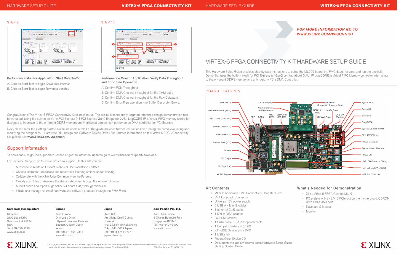
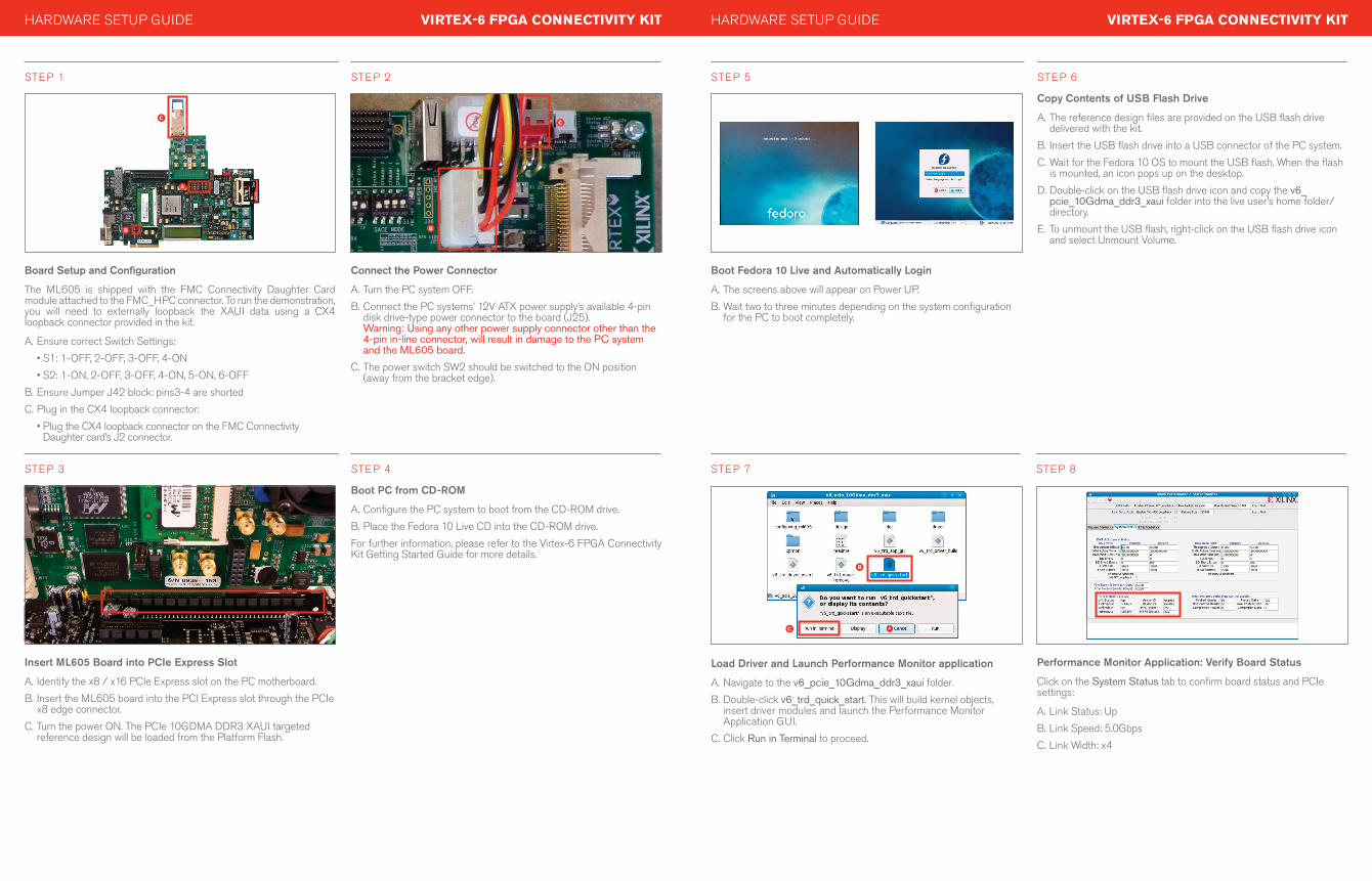
SFP DDR3 FMC (LPC) FMC (HPC) Connectivity Daughter Card Clock Generator and Synthesizer CX4 Connector USB 2.0 (Host) 12V Wall Power 12V ATX Power USB 2.0 (Device) Push Buttons (SW5-SW9) MGT Port (J26-J29) 16x2 LCD Character Display X8 PCI Express Ethernet System ACE Prog (SW4) Switch S1 Switch S2 SystemACE RST (SW3) CPU RST (SW10) PMBus Controller System Monitor Headers PMBus (J3) GPIO DIP Switch (SW1) MGT Clock (J30 & J31) USB to UART (J21) USB JTAG (J22) Platform Flash (U27) DVI Output User Clock (J55-J58) BPI Flash (U4) GPIO LEDs FOR MORE INFORMATION GO TO WWW.XILINX.COM/V6CONNKIT This Hardware Setup Guide provides step-by-step instructions to setup the ML605 board, the FMC daughter card, and run the pre-built Demo that uses the built-in block for PCI Express (x4Gen2 configuration), XAUI IP LogiCORE, a Virtual FIFO Memory controller interfacing to the on-board DDR3 memory and a third-party PCIe DMA Controller. Kit Contents ML605 board and FMC Connectivity Daughter Card CX4 Loopback Connector Universal 12V power supply 2 USB A / Mini-B cables 1 ethernet Cat5 cable 1 DVI-to-VGA adapter Four SMA cables 1 SATA cable, 1 SATA loopback cable 1 CompactFlash card (2GB) Xilinx ISE Design Suite DVD 1 USB stick Fedora Core 10 Live CD Documents include a welcome letter, Hardware Setup Guide, Getting Started Guide What’s Needed for Demonstration Xilinx Virtex-6 FPGA Connectivity Kit PC system with a x8/x16 PCIe slot on the motherboard, CDROM drive and a USB port Keyboard & Mouse Monitor VIRTEX-6 FPGA CONNECTIVITY KIT VIRTEX-6 FPGA CONNECTIVITY KIT HARDWARE SETUP GUIDE HARDWARE SETUP GUIDE VIRTEX-6 FPGA CONNECTIVITY KIT HARDWARE SETUP GUIDE BOARD FEATURESXXXXXXXXXXXXXXXXXXXXXXXXXXXXXXXXXXXXXXXXXXXXXXXXXXXXXXXXXXX Congratulations! The Virtex-6 FPGA Connectivity Kit is now set up. The pre-built connectivity targeted reference design demonstration has been tested, using the built-in block for PCI Express (x4 PCI Express Gen2 Endpoint), XAUI LogiCORE IP, a Virtual FIFO memory controller designed to interface to the on-board DDR3 memory, and Northwest Logic’s high performance DMA controller for PCI Express. Next, please refer the Getting Started Guide included in this kit. The guide provides further instructions on running the demo, evaluating and modifying the design files – Hardware RTL design and Software Device Driver. For updated information on this Virtex-6 FPGA Connectivity Kit, please visit www.xilinx.com/v6connkit. Support Information To download Design Tools, generate license or get the latest tool updates go to www.xilinx.com/support/download. For Technical Support, go to www.xilinx.com/support. On this site you can: Subscribe to Alerts on Product Technical Documentation updates Choose instructor-led classes and recorded e-learning options under Training Collaborate with the Xilinx User Community on the Forums Quickly scan titles of Answers Database categories through the Answer Browser Submit cases and report bugs online 24 hours a day through WebCase Initiate and manage return of hardware and software products through the RMA Portal © Copyright 2010 Xilinx, Inc. XILINX, the Xilinx logo, Virtex, Spartan, ISE and other designated brands included herein are trademarks of Xilinx in the United States and other countries. All other trademarks are the property of their respective owners. Printed in the U.S.A. Xilinx Part Number: PN0402827-02 Corporate Headquarters Xilinx, Inc. 2100 Logic Drive San Jose, CA 95124 USA Tel: 408-559-7778 www.xilinx.com Europe Xilinx Europe One Logic Drive Citywest Business Campus Saggart, County Dublin Ireland Tel: +353-1-464-0311 www.xilinx.com Japan Xilinx K.K. Art Village Osaki Central Tower 4F 1-2-2 Osaki, Shinagawa-ku Tokyo 141-0032 Japan Tel: +81-3-6744-7777 japan.xilinx.com Asia Pacific Pte. Ltd. Xilinx, Asia Pacific 5 Changi Business Park Singapore 486040 Tel: +65-6407-3000 www.xilinx.com STEP 10 IIIIIIIIIIIIIIIIIIIIIIIIIIIIIIIIIIIIIIIIIIIIIIIIIIIIIIIIIIIIIIIIIIIII Performance Monitor Application: Verify Data Throughput and Error Free Operation A. Confirm PCIe Throughput. B. Confirm DMA Channel throughput for the XAUI path. C. Confirm DMA Channel throughput for the Raw Data path. D. Confirm Error Free operation - no Buffer Descriptor Errors. STEP 9 IIIIIIIIIIIIIIIIIIIIIIIIIIIIIIIIIIIIIIIIIIIIIIIIIIIIIIIIIIIIIIIIIIIIII Performance Monitor Application: Start Data Traffic A. Click on Start Test to begin XAUI data transfer. B. Click on Start Test to begin Raw data transfer.
Transcript

SFP DDR3FMC(LPC)

FMC (HPC)Connectivity Daughter Card

Clock Generatorand Synthesizer

CX4 Connector

USB 2.0(Host)

12V Wall Power

12V ATX Power

USB 2.0(Device)

Push Buttons (SW5-SW9)

MGT Port (J26-J29)

16x2 LCD Character Display

X8 PCI Express

Ethernet

System ACE

Prog (SW4)

Switch S1

Switch S2

SystemACE RST (SW3)

CPU RST (SW10)

PMBus Controller

System Monitor Headers

PMBus (J3)

GPIO DIP Switch (SW1)

MGT Clock (J30 & J31)

USB to UART (J21)

USB JTAG (J22)

Platform Flash (U27)

DVI Output

User Clock(J55-J58)

BPI Flash (U4)

GPIO LEDs

FOR MORE INFORMATION GO TO WWW.XILINX.COM/V6CONNKIT

This Hardware Setup Guide provides step-by-step instructions to setup the ML605 board, the FMC daughter card, and run the pre-built Demo that uses the built-in block for PCI Express (x4Gen2 configuration), XAUI IP LogiCORE, a Virtual FIFO Memory controller interfacing to the on-board DDR3 memory and a third-party PCIe DMA Controller.

Kit Contents• ML605 board and FMC Connectivity Daughter Card• CX4 Loopback Connector• Universal 12V power supply• 2 USB A / Mini-B cables• 1 ethernet Cat5 cable• 1 DVI-to-VGA adapter• Four SMA cables• 1 SATA cable, 1 SATA loopback cable• 1 CompactFlash card (2GB)• Xilinx ISE Design Suite DVD• 1 USB stick• Fedora Core 10 Live CD• Documents include a welcome letter, Hardware Setup Guide,

Getting Started Guide

What’s Needed for Demonstration• Xilinx Virtex-6 FPGA Connectivity Kit• PC system with a x8/x16 PCIe slot on the motherboard, CDROM

drive and a USB port• Keyboard & Mouse• Monitor

VIRTEX-6 FPGA CONNECTIVITY KITVIRTEX-6 FPGA CONNECTIVITY KIT HARDWARE SETUP GUIDEHARDWARE SETUP GUIDE

VIRTEX-6 FPGA CONNECTIVITY KIT HARDWARE SETUP GUIDE

BOARD FEATURESXXXXXXXXXXXXXXXXXXXXXXXXXXXXXXXXXXXXXXXXXXXXXXXXXXXXXXXXXXXXXX

Congratulations! The Virtex-6 FPGA Connectivity Kit is now set up. The pre-built connectivity targeted reference design demonstration has been tested, using the built-in block for PCI Express (x4 PCI Express Gen2 Endpoint), XAUI LogiCORE IP, a Virtual FIFO memory controller designed to interface to the on-board DDR3 memory, and Northwest Logic’s high performance DMA controller for PCI Express.

Next, please refer the Getting Started Guide included in this kit. The guide provides further instructions on running the demo, evaluating and modifying the design files – Hardware RTL design and Software Device Driver. For updated information on this Virtex-6 FPGA Connectivity Kit, please visit www.xilinx.com/v6connkit.

Support InformationTo download Design Tools, generate license or get the latest tool updates go to www.xilinx.com/support/download.

For Technical Support, go to www.xilinx.com/support. On this site you can:

• Subscribe to Alerts on Product Technical Documentation updates• Choose instructor-led classes and recorded e-learning options under Training• Collaborate with the Xilinx User Community on the Forums• Quickly scan titles of Answers Database categories through the Answer Browser• Submit cases and report bugs online 24 hours a day through WebCase• Initiate and manage return of hardware and software products through the RMA Portal

© Copyright 2010 Xilinx, Inc. XILINX, the Xilinx logo, Virtex, Spartan, ISE and other designated brands included herein are trademarks of Xilinx in the United States and other countries. All other trademarks are the property of their respective owners. Printed in the U.S.A. Xilinx Part Number: PN0402827-02

Corporate Headquarters

Xilinx, Inc.2100 Logic DriveSan Jose, CA 95124USATel: 408-559-7778www.xilinx.com

Europe

Xilinx EuropeOne Logic DriveCitywest Business CampusSaggart, County DublinIrelandTel: +353-1-464-0311www.xilinx.com

Japan

Xilinx K.K.Art Village Osaki Central Tower 4F1-2-2 Osaki, Shinagawa-kuTokyo 141-0032 JapanTel: +81-3-6744-7777japan.xilinx.com

Asia Pacific Pte. Ltd.

Xilinx, Asia Pacific5 Changi Business ParkSingapore 486040Tel: +65-6407-3000www.xilinx.com

STEP 10I I I I I I I I I I I I I I I I I I I I I I I I I I I I I I I I I I I I I I I I I I I I I I I I I I I I I I I I I I I I I I I I I I I I I

Performance Monitor Application: Verify Data Throughput and Error Free Operation

A. Confirm PCIe Throughput.B. Confirm DMA Channel throughput for the XAUI path.C. Confirm DMA Channel throughput for the Raw Data path.D. Confirm Error Free operation - no Buffer Descriptor Errors.

STEP 9I I I I I I I I I I I I I I I I I I I I I I I I I I I I I I I I I I I I I I I I I I I I I I I I I I I I I I I I I I I I I I I I I I I I I I

Performance Monitor Application: Start Data Traffic

A. Click on Start Test to begin XAUI data transfer.B. Click on Start Test to begin Raw data transfer.

STEP 2I I I I I I I I I I I I I I I I I I I I I I I I I I I I I I I I I I I I I I I I I I I I I I I I I I I I I I I I I I I I I I I I I I I I I I STEP 6I I I I I I I I I I I I I I I I I I I I I I I I I I I I I I I I I I I I I I I I I I I I I I I I I I I I I I I I I I I I I I I I I I I I I I

STEP 4I I I I I I I I I I I I I I I I I I I I I I I I I I I I I I I I I I I I I I I I I I I I I I I I I I I I I I I I I I I I I I I I I I I I I I STEP 8I I I I I I I I I I I I I I I I I I I I I I I I I I I I I I I I I I I I I I I I I I I I I I I I I I I I I I I I I I I I I I I I I I I I I I

Connect the Power Connector

A. Turn the PC system OFF.B. Connect the PC systems’ 12V ATX power supply’s available 4-pin

disk drive-type power connector to the board (J25). Warning: Using any other power supply connector other than the 4-pin in-line connector, will result in damage to the PC system and the ML605 board.

C. The power switch SW2 should be switched to the ON position (away from the bracket edge).

Performance Monitor Application: Verify Board Status

Click on the System Status tab to confirm board status and PCIe settings:

A. Link Status: UpB. Link Speed: 5.0GbpsC. Link Width: x4

Load Driver and Launch Performance Monitor application

A. Navigate to the v6_pcie_10Gdma_ddr3_xaui folder.B. Double-click v6_trd_quick_start. This will build kernel objects,

insert driver modules and launch the Performance Monitor Application GUI.

C. Click Run in Terminal to proceed.

Copy Contents of USB Flash Drive

A. The reference design files are provided on the USB flash drive delivered with the kit.

B. Insert the USB flash drive into a USB connector of the PC system.C. Wait for the Fedora 10 OS to mount the USB flash. When the flash

is mounted, an icon pops up on the desktop.D. Double-click on the USB flash drive icon and copy the v6_

pcie_10Gdma_ddr3_xaui folder into the live user’s home folder/directory.

E. To unmount the USB flash, right-click on the USB flash drive icon and select Unmount Volume.

Boot PC from CD-ROM

A. Configure the PC system to boot from the CD-ROM drive.B. Place the Fedora 10 Live CD into the CD-ROM drive.For further information, please refer to the Virtex-6 FPGA Connectivity Kit Getting Started Guide for more details.

VIRTEX-6 FPGA CONNECTIVITY KITVIRTEX-6 FPGA CONNECTIVITY KIT HARDWARE SETUP GUIDEHARDWARE SETUP GUIDE

STEP 1I I I I I I I I I I I I I I I I I I I I I I I I I I I I I I I I I I I I I I I I I I I I I I I I I I I I I I I I I I I I I I I I I I I I I I I STEP 5I I I I I I I I I I I I I I I I I I I I I I I I I I I I I I I I I I I I I I I I I I I I I I I I I I I I I I I I I I I I I I I I I I I I I I I

STEP 3I I I I I I I I I I I I I I I I I I I I I I I I I I I I I I I I I I I I I I I I I I I I I I I I I I I I I I I I I I I I I I I I I I I I I I I STEP 7I I I I I I I I I I I I I I I I I I I I I I I I I I I I I I I I I I I I I I I I I I I I I I I I I I I I I I I I I I I I I I I I I I I I I I

Board Setup and Configuration

The ML605 is shipped with the FMC Connectivity Daughter Card module attached to the FMC_HPC connector. To run the demonstration, you will need to externally loopback the XAUI data using a CX4 loopback connector provided in the kit.

A. Ensure correct Switch Settings:•S1: 1-OFF, 2-OFF, 3-OFF, 4-ON•S2: 1-ON, 2-OFF, 3-OFF, 4-ON, 5-ON, 6-OFF

B. Ensure Jumper J42 block: pins3-4 are shortedC. Plug in the CX4 loopback connector:

•Plug the CX4 loopback connector on the FMC Connectivity Daughter card’s J2 connector.

Boot Fedora 10 Live and Automatically Login

A. The screens above will appear on Power UP.B. Wait two to three minutes depending on the system configuration

for the PC to boot completely.

Insert ML605 Board into PCIe Express Slot

A. Identify the x8 / x16 PCIe Express slot on the PC motherboard.B. Insert the ML605 board into the PCI Express slot through the PCIe

x8 edge connector.C. Turn the power ON. The PCIe 10GDMA DDR3 XAUI targeted

reference design will be loaded from the Platform Flash.


Recommended