64
Virtex-7 FPGA VC7222 GTH and GTZ Transceiver Characterization Board User Guide UG965 (v1.4) February 11, 2015

Virtex-7 FPGA VC7222 GTH and GTZ Transceiver Characterization BoardUser Guide
UG965 (v1.4) February 11, 2015
VC7222 Transceiver Characterization Board www.xilinx.com UG965 (v1.4) February 11, 2015
DISCLAIMER
The information disclosed to you hereunder (the “Materials”) is provided solely for the selection and use of Xilinx products. To the maximum extent permitted by applicable law: (1) Materials are made available "AS IS" and with all faults, Xilinx hereby DISCLAIMS ALL WARRANTIES AND CONDITIONS, EXPRESS, IMPLIED, OR STATUTORY, INCLUDING BUT NOT LIMITED TO WARRANTIES OF MERCHANTABILITY, NON-INFRINGEMENT, OR FITNESS FOR ANY PARTICULAR PURPOSE; and (2) Xilinx shall not be liable (whether in contract or tort, including negligence, or under any other theory of liability) for any loss or damage of any kind or nature related to, arising under, or in connection with, the Materials (including your use of the Materials), including for any direct, indirect, special, incidental, or consequential loss or damage (including loss of data, profits, goodwill, or any type of loss or damage suffered as a result of any action brought by a third party) even if such damage or loss was reasonably foreseeable or Xilinx had been advised of the possibility of the same. Xilinx assumes no obligation to correct any errors contained in the Materials or to notify you of updates to the Materials or to product specifications. You may not reproduce, modify, distribute, or publicly display the Materials without prior written consent. Certain products are subject to the terms and conditions of Xilinx’s limited warranty, please refer to Xilinx’s Terms of Sale which can be viewed at www.xilinx.com/legal.htm#tos; IP cores may be subject to warranty and support terms contained in a license issued to you by Xilinx. Xilinx products are not designed or intended to be fail-safe or for use in any application requiring fail-safe performance; you assume sole risk and liability for use of Xilinx products in such critical applications, please refer to Xilinx’s Terms of Sale which can be viewed at www.xilinx.com/legal.htm#tos.
© Copyright 2013–2015 Xilinx, Inc. Xilinx, the Xilinx logo, Artix, ISE, Kintex, Spartan, Virtex, Vivado, Zynq, and other designated brands included herein are trademarks of Xilinx in the United States and other countries. All other trademarks are the property of their respective owners.
Revision HistoryThe following table shows the revision history for this document.
Date Version Revision
01/25/2013 1.0 Initial Xilinx release.
01/30/2013 1.0.1 Corrected callout links located throughout the body text back to Table 1-1, page 7. Added answer record link in References, page 61.
07/23/2013 1.1 In Table 1-4, changed nominal voltage to 1.075 V. In Figure 1-3, changed MGTZAVCC and MGTZVCCL voltages to 1.075V. Added a footnote about critical signals to Table 1-20 and Table 1-21. In Appendix C, replaced user constraints file (UCF) with Xilinx Design Constraints (XDC) information. Updated links.
09/20/2013 1.1.1 Updated the Virtex-7 FPGA VC7222 IBERT Getting Started Guide (Vivado Design Suite) (UG971) link in Appendix D, Additional Resources.
12/18/2013 1.2 Revised Table 1-7 through Table 1-12, Table 1-18, and Table 1-19. Rearranged rows in Table 1-21. Updated references in Appendix D, Additional Resources. Updated the Declaration of Conformity link in Appendix E, Regulatory and Compliance Information.
08/21/2014 1.3 The number of 7 series GTH power modules from third-party vendors supplied with the VC7222 board changed from four to two. Appendix C was renamed Master Constraints File Listing. Intersil and Lineage vendors were removed from References, page 61.
02/11/2015 1.4 Two power modules are provided with the VC7222 board—Texas Instruments PMP6577 and Bellnix BPE-37 (for 7 Series GTH Transceiver Power Module, page 13 and 7 Series GTZ Transceiver Power Module, page 15. Updated VC7222 Board XDC Listing, page 47.

VC7222 Transceiver Characterization Board www.xilinx.com 3UG965 (v1.4) February 11, 2015
Revision History . . . . . . . . . . . . . . . . . . . . . . . . . . . . . . . . . . . . . . . . . . . . . . . . . . . . . . . . . . . . . 2
Chapter 1: VC7222 Board Features and OperationVC7222 Board Features . . . . . . . . . . . . . . . . . . . . . . . . . . . . . . . . . . . . . . . . . . . . . . . . . . . . . . . 5Detailed Description . . . . . . . . . . . . . . . . . . . . . . . . . . . . . . . . . . . . . . . . . . . . . . . . . . . . . . . . . 6
Appendix A: Default Jumper and Switch Settings
Appendix B: VITA 57.1 FMC Connector Pinouts
Appendix C: Master Constraints File ListingVC7222 Board XDC Listing . . . . . . . . . . . . . . . . . . . . . . . . . . . . . . . . . . . . . . . . . . . . . . . . . . 47
Appendix D: Additional ResourcesXilinx Resources . . . . . . . . . . . . . . . . . . . . . . . . . . . . . . . . . . . . . . . . . . . . . . . . . . . . . . . . . . . . 61Solution Centers . . . . . . . . . . . . . . . . . . . . . . . . . . . . . . . . . . . . . . . . . . . . . . . . . . . . . . . . . . . . 61References . . . . . . . . . . . . . . . . . . . . . . . . . . . . . . . . . . . . . . . . . . . . . . . . . . . . . . . . . . . . . . . . . . 61
Appendix E: Regulatory and Compliance InformationDeclaration of Conformity . . . . . . . . . . . . . . . . . . . . . . . . . . . . . . . . . . . . . . . . . . . . . . . . . . 63Directives . . . . . . . . . . . . . . . . . . . . . . . . . . . . . . . . . . . . . . . . . . . . . . . . . . . . . . . . . . . . . . . . . . . 63Standards . . . . . . . . . . . . . . . . . . . . . . . . . . . . . . . . . . . . . . . . . . . . . . . . . . . . . . . . . . . . . . . . . . . 63Markings . . . . . . . . . . . . . . . . . . . . . . . . . . . . . . . . . . . . . . . . . . . . . . . . . . . . . . . . . . . . . . . . . . . 64
Table of Contents
Send Feedback

4 www.xilinx.com VC7222 Transceiver Characterization BoardUG965 (v1.4) February 11, 2015
Send Feedback

VC7222 Transceiver Characterization Board www.xilinx.com 5UG965 (v1.4) February 11, 2015
Chapter 1
VC7222 Board Features and Operation
This chapter describes the components, features, and operation of the Virtex®-7 FPGA VC7222 GTH and GTZ Transceiver Characterization Board. The VC7222 board provides the hardware environment for characterizing and evaluating the GTH and GTZ transceivers available on the Virtex-7 XC7VH580T-G2HCG1155E FPGA. The VC7222 board schematic, bill-of-material (BOM), layout files, and reference designs are available online at the Virtex-7 FPGA VC7222 Characterization Kit documentation website.
VC7222 Board Features• Virtex-7 XC7VH580T-G2HCG1155E FPGA
• Onboard power supplies for all necessary voltages
• Terminal blocks for optional use of external power supplies
• Digilent USB JTAG programming port
• System ACE™ SD controller
• Power module supporting Virtex-7 FPGA GTH transceiver power requirements
• Power module supporting Virtex-7 FPGA GTZ transceiver power requirements
• A fixed, 200 MHz 2.5V LVDS oscillator wired to multi-region clock capable (MRCC) inputs
• Two pairs of differential MRCC inputs with SMA connectors
• SuperClock-2 module supporting multiple frequencies
• Six Samtec BullsEye connector pads for the GTH transceivers and reference clocks
• Two Samtec BullsEye connector pads for the GTZ transceivers and two pairs of SMA connectors for GTZ transceiver reference clocks
• Power status LEDs
• General purpose DIP switches, LEDs, pushbuttons, and test I/O
• Two VITA 57.1 FPGA mezzanine card (FMC) high pin count (HPC) connectors
• USB-to-UART bridge
• I2C bus
• PMBus connectivity to onboard digital power supplies
• Active cooling for the FPGA
Send Feedback

6 www.xilinx.com VC7222 Transceiver Characterization BoardUG965 (v1.4) February 11, 2015
Chapter 1: VC7222 Board Features and Operation
The VC7222 board block diagram is shown in Figure 1-1.
Detailed DescriptionFigure 1-2 shows the VC7222 board described in this user guide. Each numbered feature that is referenced in Figure 1-2 is described in Table 1-1 and later sections.
The VC7222 board can be damaged by electrostatic discharge (ESD). Follow standard ESD prevention measures when handling the board.
Caution! Do not remove the rubber feet from the board. The feet provide clearance to prevent short circuits on the back side of the board.
Note: Figure 1-2 is for reference only and might not reflect the current revision of the board.
X-Ref Target - Figure 1-1
Figure 1-1: VC7222 Board Block Diagram
UG965_c1_01_070313
Push Buttons,DIP Switches,
and LEDs
SuperClock-2 ModuleInterface
GTH Transceivers
Virtex-7 FPGAXC7VH580T-G2HCG1155E
Select I/O Terminationand VTT Jacks
Analog/DigitalConverter (XADC)
FMC1 InterfaceHigh-Performance I/O
USB to UARTBridge
FMC2 InterfaceHigh-Performance I/O
I2C BusManagement
7 SeriesGTH Power Module
Interface
12V
PMBus
5V3.3V
User Clocks
System ACE SDController
Power In12VDC
PMBus
FPGA Power SourceOn-board Regulation:
VCCINT 1.0V, 20AVCCBRAM 1.0V, 10AVCCAUX 1.8V, 10AVCCAUX_IO 1.8V, 10AVCCO_HP 1.8V, 10AVCCO_0 1.8V, 7.5A
Board Utility PowerOn-board Regulation:
5.0V, 10A3.3V, 18A2.5V, 18A
GTH and GTZPower Monitoring
VCCO_HP
5V3.3V2.5V
QUAD 113QUAD 114QUAD 115QUAD 213QUAD 214QUAD 215
7 SeriesGTZ Power Module
Interface
12V
PMBus
5V3.3V
GTZ TransceiversOCTAL 300AOCTAL 300B
Send Feedback

VC7222 Transceiver Characterization Board www.xilinx.com 7UG965 (v1.4) February 11, 2015
Detailed Description
X-Ref Target - Figure 1-2
Figure 1-2: VC7222 Board Features. Callouts Listed in Table 1-1
UG965_c1_02_070313
2
3
32
1
29
3534
5 4
14
10
28 12 119
13
25
26
33
30
31
19
27
222423
17
16
18
66
7
15 36
36
37
8
20
21
Table 1-1: VC7222 Board Feature Descriptions
Figure 1-2Callout
ReferenceDesignator
FeatureDescription
1 U1 Virtex-7 XC7VH580T-G2HCG1155E FPGA
2 SW1 Power switch
3 J2 12V Mini-Fit connector
4 J131 12V ATX Connector
5 J12 12V Euro-Mag Connector
6J28, J85, J86,
J158, J159, J241GTH transceiver connector pads Q113, Q114, Q115, Q213, Q214 and Q215
7 J18, J25 GTZ transceiver connector pads O300A and O300B
8 J46, J47, J56, J57 GTZ transceiver reference clock SMAs
9 U57 USB JTAG connector (micro-B receptacle)
10 J1JTAG connector (alternate access for programming cables)
11 J30 System ACE SD card connector (back-side of board)
12 SW8 System ACE SD configuration address DIP switches
Send Feedback

8 www.xilinx.com VC7222 Transceiver Characterization BoardUG965 (v1.4) February 11, 2015
Chapter 1: VC7222 Board Features and Operation
13 SW7 System ACE SD RESET button
14 SuperClock-2 module
15 U35 200 MHz 2.5V LVDS oscillator
16 DS21 FPGA DONE status LED
17 DS25 FPGA INIT_B status LED
18 SW3 FPGA PROG_B pushbutton
19 DS11 12V power status LED
20
DS1, DS2, DS3, DS4,DS5, DS6, DS7, DS8,
DS9, DS10, DS26,DS27, DS28, DS29,
DS30
Status LEDS for FPGA logic, transceiver and utility power
21 SW10 Core power regulation enable switches
22 J75 Core power terminal block
23 J72 GTH transceiver power terminal block
24 J73 GTZ transceiver power terminal block
25 GTH transceiver power supply module
26 GTZ transceiver power supply module
27 J26 PMBUS connector
28 J79 Connector for USB to UART bridge (mini-B receptacle)
29 J121 Power connector for active heatsink
30DS13, DS14, DS15,DS16, DS17, DS18,
DS19, DS20User LEDs (active high)
31 SW4, SW5 User pushbuttons (active high)
32 SW2 User DIP switches (active high)
33 J125 User I/O header
34 JA2 FMC1 connector
35 JA3 FMC2 connector
36 J98, J99, J100, J101 SMA connectors to differential MRCC pins on FPGA
37 J141, J142, R233Jumpers and potentiometer for XADC referenceand analog supply set-up
Table 1-1: VC7222 Board Feature Descriptions (Cont’d)
Figure 1-2Callout
ReferenceDesignator
FeatureDescription
Send Feedback

VC7222 Transceiver Characterization Board www.xilinx.com 9UG965 (v1.4) February 11, 2015
Detailed Description
Power Management
Board 12V Input Power
VC7222 board receives 12V main power through J2 (callout 3, Figure 1-2) using the 12V AC adapter that ships with the board. J2 is a 6-pin (2 x 3), right angle, Mini-Fit connector.
Caution! When supplying 12V through J2, use only the power supply provided for use with this board (Xilinx part number 3800033).
Caution! Do NOT use a 6-pin, PC ATX power supply connector with J2. The pinout of the 6-pin, PC ATX connector is not compatible J2 and the board will be damaged if an attempt is made to power it from a PC ATX power supply connector.
12V power can also be provided through:
• Connector J131 which accepts an ATX hard drive, 4-pin, power plug
• Euro-Mag terminal block J12 which can be connected to a bench-top power supply
Caution! Because terminal block J12 provides no reverse polarity protection, use a power supply with a current limit set at 6A max.
Caution! Do NOT apply 12V power to more than a single input source. For example, do not apply power to J2 and J131 at the same time.
Power Switch
Main board power is turned on or off using switch SW1 (callout 2, Figure 1-2). When the switch is in the ON position, power is applied to the board and green LED DS11 illuminates (callout 19, Figure 1-2).
Onboard Power Regulation
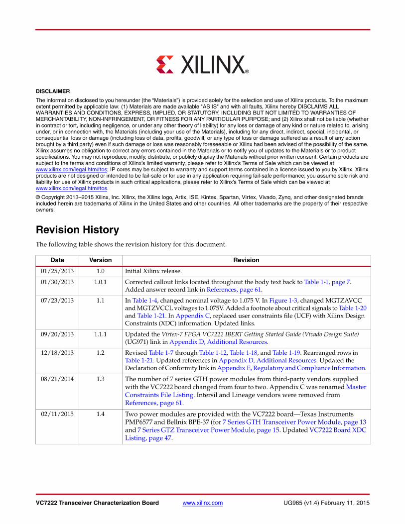
Figure 1-3 shows the onboard power supply architecture.
Send Feedback
10 www.xilinx.com VC7222 Transceiver Characterization BoardUG965 (v1.4) February 11, 2015
Chapter 1: VC7222 Board Features and Operation
The VC7222 board uses power regulators and PMBus compliant digital PWM system controllers from Texas Instruments to supply the FPGA logic and utility voltages listed in
X-Ref Target - Figure 1-3
Figure 1-3: VC7222 Board Power Supply Block Diagram
UG965_c1_03_070313
MGTZVCCH
MGTZVCCL
MGTZAVCC
VCCAUX
VCCINT
VCCAUX_IO
VCCBRAM
VCCO_0
VCCO_HP
Power Supply
12V PWR INJ2 or J12or J131 Power Controller 1
UCD9248PFCU9
Switching Regulator (2 Phases)1.0V at 40A max
U5, U51
Switching Regulator5.0V at 10A max
U2
Switching Regulator3.3V at 18A max
U13
UTIL_5V0
UTIL_3V3
Switching Regulator2.5V at 18A max
U52 UTIL_2V5
Switching Regulator1.8V at 10A max
U6
Switching Regulator1.0V at 10A max
Power Controller 2
Switching Regulator1.8V at 10A max
U46
Switching Regulator1.8V at 10A max
U50
Switching Regulator1.8V at 10A max
U10UCD9248PFC
7 Series GTH Power Module
MGTAVCC: 1.05V at 12.0A max
MGTAVTT: 1.2V at 8.0A max
MGTVCCAUX: 1.8V at 2.6A max
7 Series GTZ Power Module
MGTZAVCC: 1.075V at 6.0A max
MGTZVCCL: 1.075V at 1.3A max
MGTZVCCH: 1.8V at 0.3A max
MGTVCCAUX
MGTAVTT
MGTAVCC
Send Feedback

VC7222 Transceiver Characterization Board www.xilinx.com 11UG965 (v1.4) February 11, 2015
Detailed Description
Table 1-2. The board can also be configured to use an external bench power supply for each voltage. See Using External Power Sources.
Table 1-2: Onboard Power System Devices
DeviceReference
Designator(s)Description
Power RailNet Name
Voltage
Core Power
UCD9248PFC U9 PMBus compliant digital PWM system controller (address = 52)
PTD08A020W U5, U51Adjustable(1) switching regulator, 40A (two phases at 20A/phase), 0.6V to 3.6V VCCINT 1.0V
PTD08D210W(VOUTA)
U6
Adjustable(1) switching regulator, Dual 10A, 0.6V to 3.6VVCCAUX 1.8V
PTD08D210W(VOUTB)
Adjustable(1) switching regulator, Dual 10A, 0.6V to 3.6VVCCBRAM 1.0V
UCD9248PFC U10 PMBus compliant digital PWM system controller (address = 53)
PTD08D210W(VOUTA)
U50
Adjustable(1) switching regulator, Dual 10A, 0.6V to 3.6VVCCAUX_IO 1.8V
PTD08D210W(VOUTB)
Adjustable(1) switching regulator, Dual 10A, 0.6V to 3.6VVCCO_HP 1.8V
PTD08A006W U46 Adjustable(1) switching regulator, 10A, 0.6V to 3.6V VCCO_0 1.8V
GTH Transceivers (monitoring only)
UCD9248PFC(2) U11 PMBus compliant digital PWM system controller (address = 54)
GTZ Transceivers (monitoring only)
UCD9248PFC(3) U18 PMBus compliant digital PWM system controller (address = 55)
Utility
PTH12060W U2 Fixed switching regulator, 10A UTIL_5V0 5.0V
PTH12020W U13 Fixed switching regulator, 18A UTIL_3V3 3.3V
PTH12020W U52 Fixed switching regulator, 18A UTIL_2V5 2.5V
XADC((4)
ADP123 U43 Fixed LDO regulator VCCADC_ADP 1.8V
REF3012 U45 Fixed LDO regulator VREFP_3012 1.25V
System ACE SD
ADP123 U21 Fixed LDO Regulator VCC1V2 1.2V
Notes: 1. The output voltages of regulators controlled by a UCD9248 can be reprogrammed using the Texas Instruments Fusion Digital Power
Designer application (www.ti.com/tool/fusion_digital_power_designer). However, extreme caution must be taken when attempting to modify any of the onboard regulators. An incorrectly programmed regulator can damage onboard components.
2. The UCD9248PFC (U11) at Address 54 monitors MGTAVCC, MGTAVTT, and MGTVCCAUX rail voltage and current levels which can be observed in real time using the Texas Instruments Fusion Digital Power Designer application (see Monitoring Voltage and Current, page 13). Transceiver supply voltages cannot be changed from this controller.
3. The UCD9248PFC (U18) at Address 55 monitors MGTZAVCC, MGTZVCCL, and MGTZVCCH rail voltage and current levels which can be observed in real time using the Texas Instruments Fusion Digital Power Designer application (see Monitoring Voltage and Current, page 13). Transceiver supply voltages cannot be changed from this controller.
4. For information on XADC see 7 Series FPGAs and Zynq-7000 All Programmable SoC XADC Dual 12-Bit 1 MSPS Analog-to-Digital Converter User Guide (UG480) [Ref 1].
Send Feedback

12 www.xilinx.com VC7222 Transceiver Characterization BoardUG965 (v1.4) February 11, 2015
Chapter 1: VC7222 Board Features and Operation
Using External Power Sources
The maximum output current rating for each power regulator is listed in Table 1-2. If a design exceeds this value on any core power rail, power for that rail must be supplied externally through the 14-position core power terminal block J75 shown in Figure 1-4 (callout 22, Figure 1-2) using a supply capable of providing the required current.
Caution! The SW10 power regulator enable switch (callout 21, Figure 1-2) (see Disabling Onboard Power) must be set to the OFF position before turning ON the main power switch (SW1) and applying external power to the corresponding rail input pin on the core power terminal block J75 (callout 22, Figure 1-2).
Caution! The core power terminal block J75 has a maximum load current contact rating of 24A.
X-Ref Target - Figure 1-4
Figure 1-4: Core Power Terminal Block J75
UG965_c1_04_121812
Send Feedback

VC7222 Transceiver Characterization Board www.xilinx.com 13UG965 (v1.4) February 11, 2015
Detailed Description
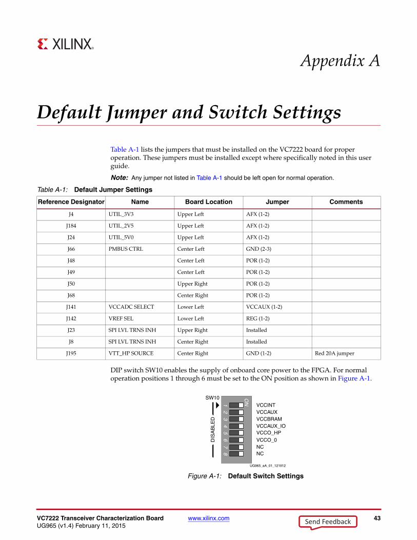
Disabling Onboard Power
Each core power regulator can be disabled through the 8-position regulator enable DIP switch, SW10 as shown in Figure 1-5. A switch in the ON position means the rail is supplied by an onboard regulator. Setting a switch in the opposite (OFF) position disables onboard power for that rail. SW10 is shown in Figure 1-2 as callout 21.
Default Jumper and Switch Positions
A list of jumpers and switches and their required positions for normal board operation is provided in Appendix A, Default Jumper and Switch Settings.
Monitoring Voltage and Current
Voltage and current monitoring and control are available for FPGA core and transceiver power rails through Texas Instruments' Fusion Digital Power graphical user interface (GUI). The four onboard TI power controllers (U9 at PMBUS address 52, U10 at PMBUS address 53, U11 at PMBUS address 54, and U18 at PMBUS address 55) are wired to the same PMBus. The PMBus connector, J26 (callout 27, Figure 1-2), is provided for use with the TI USB Interface Adapter PMBus pod and associated TI GUI.
References
More information about the power system components used by the VC7222 board are available from the Texas Instruments digital power website [Ref 2].
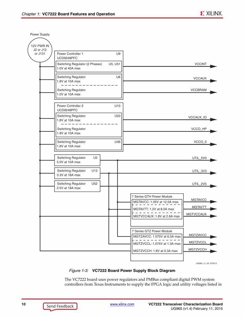
7 Series GTH Transceiver Power Module
The 7 series GTH transceiver power module (callout 25, Figure 1-2) supplies MGTAVCC, MGTAVTT and MGTVCCAUX voltages to the FPGA GTH transceivers. Two 7 series GTH power modules from third-party vendors are provided with the VC7222 board for evaluation, Texas Instruments PMP6577 and Bellnix BPE-37. Either of the two GTH modules can be plugged into connectors J29 and J102 in the outlined and labeled power module location shown in Figure 1-6.
X-Ref Target - Figure 1-5
Figure 1-5: Core Power Regulator Enable Switches SW10
UG965_c1_05_121812
Send Feedback
14 www.xilinx.com VC7222 Transceiver Characterization BoardUG965 (v1.4) February 11, 2015
Chapter 1: VC7222 Board Features and Operation
Caution! To ensure proper operation, do not plug a GTZ power module into the GTH power module location shown in Figure 1-6. Pay close attention when connecting the GTH or the GTZ power modules to the board. Both power modules have the same mechanical footprint and can be plugged into either the GTH or GTZ board interface.
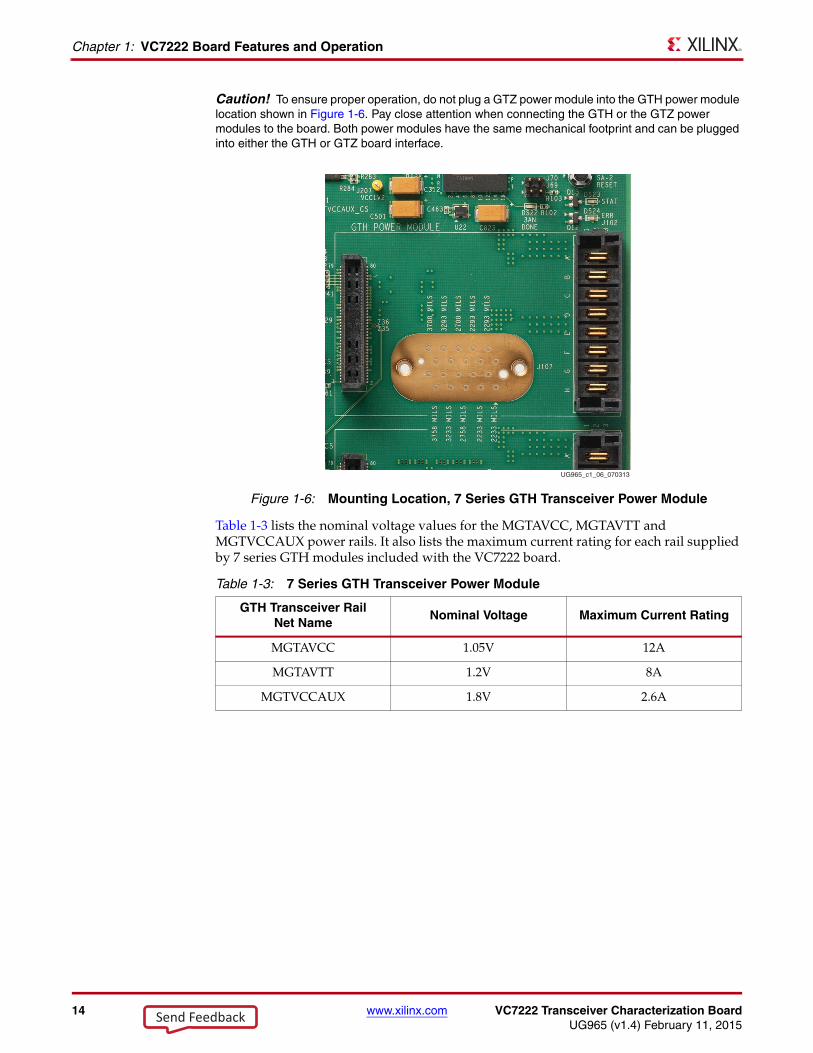
Table 1-3 lists the nominal voltage values for the MGTAVCC, MGTAVTT and MGTVCCAUX power rails. It also lists the maximum current rating for each rail supplied by 7 series GTH modules included with the VC7222 board.
X-Ref Target - Figure 1-6
Figure 1-6: Mounting Location, 7 Series GTH Transceiver Power Module
Table 1-3: 7 Series GTH Transceiver Power Module
GTH Transceiver RailNet Name
Nominal Voltage Maximum Current Rating
MGTAVCC 1.05V 12A
MGTAVTT 1.2V 8A
MGTVCCAUX 1.8V 2.6A
UG965_c1_06_070313
Send Feedback

VC7222 Transceiver Characterization Board www.xilinx.com 15UG965 (v1.4) February 11, 2015
Detailed Description
The GTH transceiver power rails also have corresponding inputs on the GTH transceiver power terminal block J72 as shown in Figure 1-7 to supply each voltage independently from a bench-top power source. J72 is shown in Figure 1-2 as callout 23.
Caution! The 7 series GTH module MUST be removed when providing external power to the GTH transceiver rails.
Information about the 7 series GTH power supply modules included with the VC7222 Characterization Kit is available from the vendor websites [Ref 3].
7 Series GTZ Transceiver Power Module
The 7 series GTZ transceiver power module (callout 26, Figure 1-2) supplies MGTZAVCC, MGTZVCCL and MGTZVCCH voltages to the FPGA GTZ transceivers. Two 7 series GTZ power modules from third-party vendors are provided with the VC7222 board for evaluation, Texas Instruments PMP6577 and Bellnix BPE-37. Either of the two GTZ modules can be plugged into connectors J5 and J71 in the outlined and labeled power module location shown in Figure 1-8.
X-Ref Target - Figure 1-7
Figure 1-7: GTH Transceiver Power Terminal Block J72
UG965_c1_07_121912
Send Feedback

16 www.xilinx.com VC7222 Transceiver Characterization BoardUG965 (v1.4) February 11, 2015
Chapter 1: VC7222 Board Features and Operation
Caution! To ensure proper operation, do not plug a GTH power module into the GTZ power module location shown in Figure 1-8. Pay close attention when connecting the GTH or the GTZ power modules to the board. Both power modules have the same mechanical footprint and can be plugged into either the GTH or GTZ board interface.
Table 1-4 lists the nominal voltage values for the MGTZAVCC, MGTZVCCL and MGTZVCCH power rails. It also lists the maximum current rating for each rail supplied by 7 series GTZ modules included with the VC7222 board.
X-Ref Target - Figure 1-8
Figure 1-8: Mounting Location, 7 Series GTZ Transceiver Power Module
Table 1-4: 7 Series GTZ Transceiver Power Module
GTZ Transceiver RailNet Name
Nominal Voltage Maximum Current Rating
MGTZVCC 1.075V 6A
MGTZVCCL 1.075V 1.3A
MGTZVCCH 1.8V 0.300A
UG965_c1_08_121912
Send Feedback

VC7222 Transceiver Characterization Board www.xilinx.com 17UG965 (v1.4) February 11, 2015
Detailed Description
The GTZ transceiver power rails also have corresponding inputs on the GTZ transceiver power terminal block J73 as shown in GTZ Transceiver Power Terminal Block J73 Figure 1-9 to supply each voltage independently from a bench-top power source. J73 is shown in Figure 1-2 as callout 24.
Caution! The 7 series GTZ module MUST be removed when providing external power to the GTZ transceiver rails.
Caution! The GTZ transceiver power terminal block J73 has a maximum load current contact rating of 24A.
Information about the two 7 series GTZ power supply modules included with the VC7222 kit is available from the vendor websites [Ref 3].
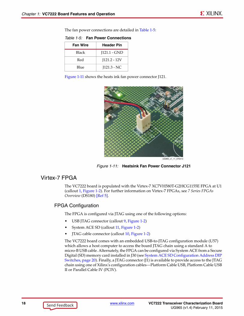
Active Heat Sink Power Connector
Callout 29, Figure 1-2
An active heat sink (Figure 1-10) is provided for the FPGA. A 12V fan is affixed to the heats ink and is powered from the 3-pin friction lock header J121 (Figure 1-11).
X-Ref Target - Figure 1-9
Figure 1-9: GTZ Transceiver Power Terminal Block J73
UG965_c1_09_121912
X-Ref Target - Figure 1-10
Figure 1-10: Active FPGA Heatsink
UG965_c1_10_070313
Send Feedback
18 www.xilinx.com VC7222 Transceiver Characterization BoardUG965 (v1.4) February 11, 2015
Chapter 1: VC7222 Board Features and Operation
The fan power connections are detailed in Table 1-5:
Figure 1-11 shows the heats ink fan power connector J121.
Virtex-7 FPGAThe VC7222 board is populated with the Virtex-7 XC7VH580T-G2HCG1155E FPGA at U1 (callout 1, Figure 1-2). For further information on Virtex-7 FPGAs, see 7 Series FPGAs Overview (DS180) [Ref 5].
FPGA Configuration
The FPGA is configured via JTAG using one of the following options:
• USB JTAG connector (callout 9, Figure 1-2)
• System ACE SD (callout 11, Figure 1-2)
• JTAG cable connector (callout 10, Figure 1-2)
The VC7222 board comes with an embedded USB-to-JTAG configuration module (U57) which allows a host computer to access the board JTAG chain using a standard A to micro-B USB cable. Alternately, the FPGA can be configured via System ACE from a Secure Digital (SD) memory card installed in J30 (see System ACE SD Configuration Address DIP Switches, page 20). Finally, a JTAG connector (J1) is available to provide access to the JTAG chain using one of Xilinx's configuration cables—Platform Cable USB, Platform Cable USB II or Parallel Cable IV (PCIV).
Table 1-5: Fan Power Connections
Fan Wire Header Pin
Black J121.1 - GND
Red J121.2 - 12V
Blue J121.3 - NC
X-Ref Target - Figure 1-11
Figure 1-11: Heatsink Fan Power Connector J121
UG965_c1_11_070313
Send Feedback
VC7222 Transceiver Characterization Board www.xilinx.com 19UG965 (v1.4) February 11, 2015
Detailed Description
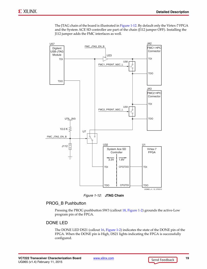
The JTAG chain of the board is illustrated in Figure 1-12. By default only the Virtex-7 FPGA and the System ACE SD controller are part of the chain (J112 jumper OFF). Installing the J112 jumper adds the FMC interfaces as well.
PROG_B Pushbutton
Pressing the PROG pushbutton SW3 (callout 18, Figure 1-2) grounds the active-Low program pin of the FPGA.
DONE LED
The DONE LED DS21 (callout 16, Figure 1-2) indicates the state of the DONE pin of the FPGA. When the DONE pin is High, DS21 lights indicating the FPGA is successfully configured.
X-Ref Target - Figure 1-12
Figure 1-12: JTAG Chain
UG965_c1_12_070313
FMC1_PRSNT_M2C_L
FMC2_PRSNT_M2C_L
FMC1 HPCConnector
TDI
TDO
JA2
FMC2 HPCConnector
TDI
TDO
JA3
U23
Virtex-7FPGA
TDI
TDO
U1
U57
DigilentUSB-JTAG
Module
TDI
TDO
System Ace SDController
TDI
TDO
U32
CFGTDO
CFGTDI
U59
U58
FMC_JTAG_EN_B
U7
3.3V 1.8V
UTIL_3V3
10.0 K
J112
FMC_JTAG_EN_B
Send Feedback

20 www.xilinx.com VC7222 Transceiver Characterization BoardUG965 (v1.4) February 11, 2015
Chapter 1: VC7222 Board Features and Operation
INIT LED
The dual-color INIT LED DS25 (callout 17, Figure 1-2) indicates the FPGA initialization status. During FPGA initialization the INIT LED illuminates RED. When FPGA initialization has completed the LED illuminates GREEN.
System ACE SD ControllerThe onboard System ACE SD controller U32 allows storage of multiple configuration files on a Secure Digital (SD) card. These configuration files can be used to program the FPGA. The SD card connects to the SD card connector J30 (callout 11, Figure 1-2) located directly below the System ACE SD controller on the back side of the board.
System ACE SD Controller Reset
Pressing the SASD RESET pushbutton SW7 (callout 13, Figure 1-2) resets the System ACE SD controller. The reset pin is an active-Low input.
System ACE SD Configuration Address DIP Switches
DIP switch SW8 shown in Figure 1-13 selects one of the eight configuration bitstream addresses in the SD memory card. A switch is in the ON position if set to the far right and in the OFF position if set to the far left. The MODE bit (switch position 4) is not used and can be set either ON or OFF. SW8 is shown in Figure 1-2 as callout 12.
The switch settings for selecting each address are shown in Table 1-6.
X-Ref Target - Figure 1-13
Figure 1-13: Configuration Address DIP Switch (SW8)
Table 1-6: SW8 DIP Switch Configuration
Configuration Bitstream Address ADR2 ADR1 ADR0
0 ON ON ON
1 ON ON OFF
2 ON OFF ON
3 ON OFF OFF
4 OFF ON ON
5 OFF ON OFF
6 OFF OFF ON
7 OFF OFF OFF
UG965_c1_13_070313
ADR0ADR1ADR2
23
4
SW8
1
MODE
ON
SYSACE-2 CFG
Send Feedback

VC7222 Transceiver Characterization Board www.xilinx.com 21UG965 (v1.4) February 11, 2015
Detailed Description
200 MHz 2.5V LVDS OscillatorU35 (callout 15, Figure 1-2).
The VC7222 board has one 200 MHz 2.5V LVDS oscillator (U35) connected to multi-region clock capable (MRCC) inputs on the FPGA. Table 1-7 lists the FPGA pin connections to the LVDS oscillator.
Table 1-7
Differential SMA MRCC Pin InputsCallout 36, Figure 1-2.
The VC7222 board provides two pairs of differential SMA transceiver clock inputs that can be used for connecting to an external function generator. The FPGA MRCC pins are connected to the SMA connectors as shown in Table 1-8.
SuperClock-2 ModuleCallout 14, Figure 1-2.
The SuperClock-2 module connects to the clock module interface connector (J82) and provides a programmable, low-noise and low-jitter clock source for the VC7222 board. The clock module maps to FPGA I/O by way of 24 control pins, 3 LVDS pairs, 1 regional clock pair, and 1 reset pin. Table 1-9 shows the FPGA I/O mapping for the SuperClock-2 module interface. The VC7222 board also supplies UTIL_5V0, UTIL_3V3, UTIL_2V5 and VCCO_HP input power to the clock module interface.
Table 1-7: LVDS Oscillator MRCC Connections
FPGA (U1) SchematicNet Name
Device (U35)
Pin Function Direction IOSTANDARD Pin Function Direction
AL24 SYSTEM CLOCK_P Input LVDS LVDS_OSC_P 4 200 MHz LVDS oscillator Output
AL25 SYSTEM CLOCK_N Input LVDS LVDS_OSC_N 5 201 MHz LVDS oscillator Output
Table 1-8: Differential SMA Clock Connections
FPGA (U1)Schematic Net Name SMA Connector
Pin Function Direction IOSTANDARD
AK32 USER CLOCK_1_P Input LVDS CLK_DIFF_1_P J99
AL32 USER CLOCK_1_N Input LVDS CLK_DIFF_1_N J100
AK3 USER CLOCK_2_P Input LVDS CLK_DIFF_2_P J98
AL3 USER CLOCK_2_N Input LVDS CLK_DIFF_2_N J101
Send Feedback

22 www.xilinx.com VC7222 Transceiver Characterization BoardUG965 (v1.4) February 11, 2015
Chapter 1: VC7222 Board Features and Operation
Table 1-9: SuperClock-2 FPGA I/O Mapping
FPGA (U1) SchematicNet Name
J82 Pin
Pin Function Direction IOSTANDARD Pin Function Direction
AK8 Clock recovery Input LVDS CM_LVDS1_P 1 Clock recovery Output
AL8 Clock recovery Input LVDS CM_LVDS1_N 3 Clock recovery Output
AE6 Clock recovery Input LVDS CM_LVDS2_P 9 Clock recovery Output
AF5 Clock recovery Input LVDS CM_LVDS2_N 11 Clock recovery Output
AG1 Clock recovery Output LVDS CM_LVDS3_P 17 Clock recovery Input
AH1 Clock recovery Output LVDS CM_LVDS3_N 19 Clock recovery Input
AJ11 Regional clock Input LVDS CM_GCLK_P 25 Global clock Output
AJ10 Regional clock Input LVDS CM_GCLK_N 27 Global clock Output
AF8 Control I/O In/Out LVCMOS18 CM_CTRL_0 61 NC -
AH9 Control I/O In/Out LVCMOS18 CM_CTRL_1 63 NC -
AH8 Control I/O In/Out LVCMOS18 CM_CTRL_2 65 NC -
AJ9 Control I/O Output LVCMOS18 CM_CTRL_3 67 DEC Input
AJ8 Control I/O Output LVCMOS18 CM_CTRL_4 69 INC Input
AM10 Control I/O Output LVCMOS18 CM_CTRL_5 71 ALIGN Input
AM9 Control I/O In/Out LVCMOS18 CM_CTRL_6 73 NC -
AF12 Control I/O In/Out LVCMOS18 CM_CTRL_7 75 NC -
AF9 Control I/O In/Out LVCMOS18 CM_CTRL_8 77 NC -
AG9 Control I/O In/Out LVCMOS18 CM_CTRL_9 79 LOL
AG12 Control I/O Output LVCMOS18 CM_CTRL_10 81 INT_ALRM Input
AH12 Control I/O Output LVCMOS18 CM_CTRL_11 83 C1B Input
AP10 Control I/O Output LVCMOS18 CM_CTRL_12 85 C2B Input
AP9 Control I/O Output LVCMOS18 CM_CTRL_13 87 C3B Input
AK12 Control I/O Output LVCMOS18 CM_CTRL_14 89 C1A Input
AL12 Control I/O Output LVCMOS18 CM_CTRL_15 91 C2A Input
AN12 Control I/O In/Out LVCMOS18 CM_CTRL_16 93 NC -
AN11 Control I/O Output LVCMOS18 CM_CTRL_17 95 CS0_C3A Input
AN9 Control I/O Output LVCMOS18 CM_CTRL_18 97 CS1_C4A Input
Send Feedback
VC7222 Transceiver Characterization Board www.xilinx.com 23UG965 (v1.4) February 11, 2015
Detailed Description
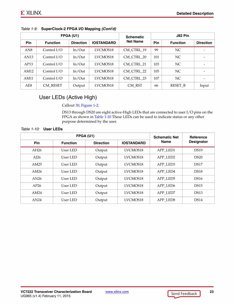
User LEDs (Active High)Callout 30, Figure 1-2.
DS13 through DS20 are eight active-High LEDs that are connected to user I/O pins on the FPGA as shown in Table 1-10 These LEDs can be used to indicate status or any other purpose determined by the user.
AN8 Control I/O In/Out LVCMOS18 CM_CTRL_19 99 NC -
AN13 Control I/O In/Out LVCMOS18 CM_CTRL_20 101 NC -
AP13 Control I/O In/Out LVCMOS18 CM_CTRL_21 103 NC -
AM12 Control I/O In/Out LVCMOS18 CM_CTRL_22 105 NC -
AM11 Control I/O In/Out LVCMOS18 CM_CTRL_23 107 NC -
AE8 CM_RESET Output LVCMOS18 CM_RST 66 RESET_B Input
Table 1-9: SuperClock-2 FPGA I/O Mapping (Cont’d)
FPGA (U1) SchematicNet Name
J82 Pin
Pin Function Direction IOSTANDARD Pin Function Direction
Table 1-10: User LEDs
FPGA (U1) Schematic Net Name
Reference DesignatorPin Function Direction IOSTANDARD
AH26 User LED Output LVCMOS18 APP_LED1 DS19
AJ26 User LED Output LVCMOS18 APP_LED2 DS20
AM25 User LED Output LVCMOS18 APP_LED3 DS17
AM26 User LED Output LVCMOS18 APP_LED4 DS18
AN26 User LED Output LVCMOS18 APP_LED5 DS16
AP26 User LED Output LVCMOS18 APP_LED6 DS15
AM24 User LED Output LVCMOS18 APP_LED7 DS13
AN24 User LED Output LVCMOS18 APP_LED8 DS14
Send Feedback

24 www.xilinx.com VC7222 Transceiver Characterization BoardUG965 (v1.4) February 11, 2015
Chapter 1: VC7222 Board Features and Operation
User DIP Switches (Active High) and I/O HeaderCallout 32, Figure 1-2.
The DIP switch SW2 provides a set of eight active-High switches that are connected to user I/O pins on the FPGA as shown in Table 1-11. These pins can be used to set control pins or any other purpose determined by the user. Six of the eight I/Os also map to 2 x 6 test header J125 providing external access for these pins (callout 33, Figure 1-2.).
Figure 1-14 Shows the user test I/O connector J125 (Callout 26, Figure 1-2).
User Pushbuttons (Active High)Callout 31, Figure 1-2.
SW4 and SW5 are active-High user pushbuttons that are connected to user I/O pins on the FPGA as shown in Table 1-12. These switches can be used for any purpose determined by the user.
Table 1-11: User DIP Switches
FPGA (U1) SchematicNet Name
SW2 DIP Switch Pin
J125 Test Header PinPin Function Direction IOSTANDARD
AD26 User switch Input LVCMOS18 USER_SW1 1 2
AE26 User switch Input LVCMOS18 USER_SW2 2 4
AC26 User switch Input LVCMOS18 USER_SW3 3 6
AC27 User switch Input LVCMOS18 USER_SW4 4 8
AE27 User switch Input LVCMOS18 USER_SW5 5 10
AF27 User switch Input LVCMOS18 USER_SW6 6 12
AG27 User switch Input LVCMOS18 USER_SW7 7 -
AH27 User switch Input LVCMOS18 USER_SW8 8 -
X-Ref Target - Figure 1-14
Figure 1-14: User Test I/O
UG965_c1_14_070313
USER_SW1
98765432
10
1
1211
J125
GND
USER_SW2USER_SW3USER_SW4USER_SW5USER_SW6
Table 1-12: User Pushbuttons
FPGA (U1) SchematicNet Name
Reference DesignatorPin Function Direction IOSTANDARD
AL22 User pushbutton Input LVCMOS18 USER_PB1 SW5
AM22 User pushbutton Input LVCMOS18 USER_PB2 SW4
Send Feedback
VC7222 Transceiver Characterization Board www.xilinx.com 25UG965 (v1.4) February 11, 2015
Detailed Description
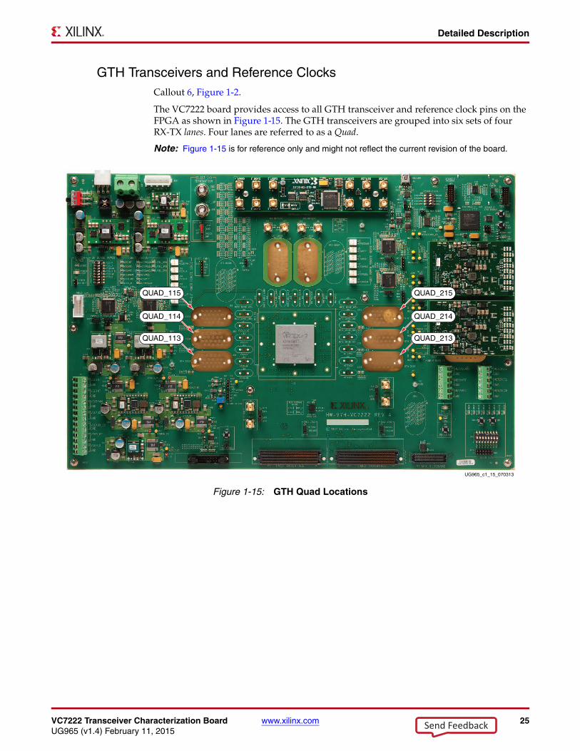
GTH Transceivers and Reference ClocksCallout 6, Figure 1-2.
The VC7222 board provides access to all GTH transceiver and reference clock pins on the FPGA as shown in Figure 1-15. The GTH transceivers are grouped into six sets of four RX-TX lanes. Four lanes are referred to as a Quad.
Note: Figure 1-15 is for reference only and might not reflect the current revision of the board.X-Ref Target - Figure 1-15
Figure 1-15: GTH Quad Locations
UG965_c1_15_070313
QUAD_115
QUAD_114
QUAD_113
QUAD_214
QUAD_213
QUAD_215
Send Feedback

26 www.xilinx.com VC7222 Transceiver Characterization BoardUG965 (v1.4) February 11, 2015
Chapter 1: VC7222 Board Features and Operation
Each GTH Quad and its associated reference clocks (CLK0 and CLK1) are brought out to a connector pad which interfaces with Samtec BullsEye connectors used with the Samtec HDR-155805-01-BEYE cable assembly. Contact Samtec, Inc. for information about this or other cable assemblies. Figure 1-16 A shows the connector pad. Figure 1-16 B shows the connector pinout.
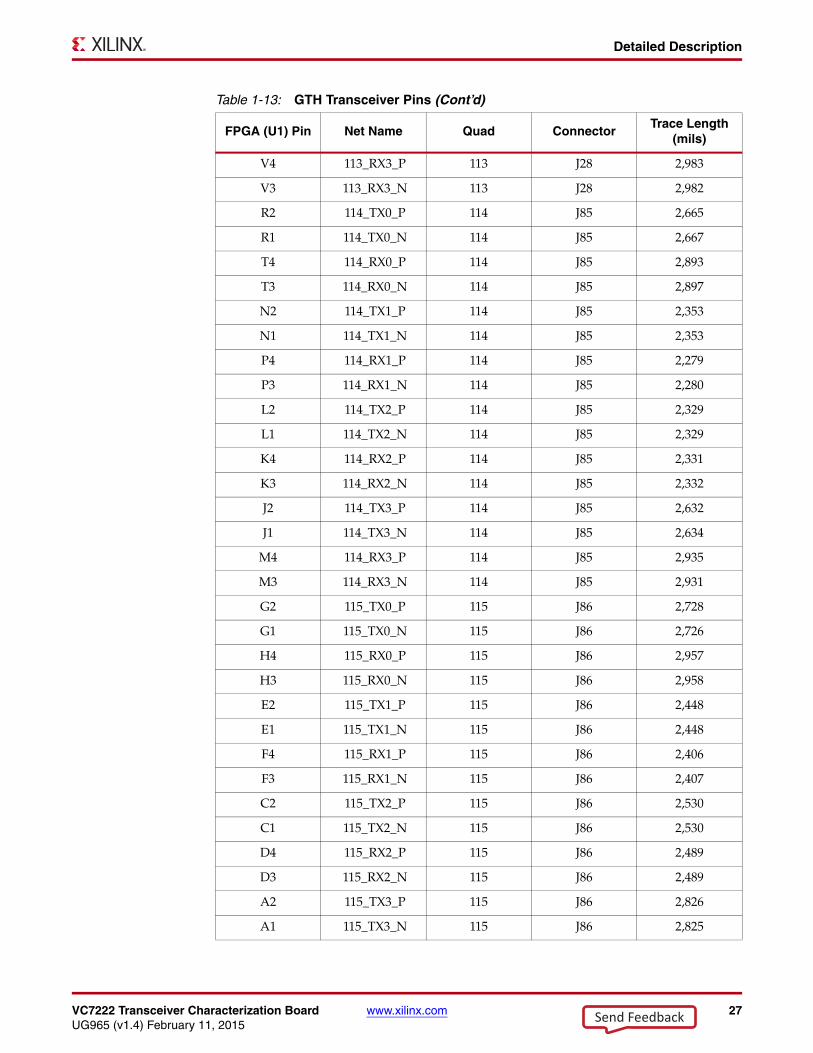
Information for each GTH transceiver pin is shown in Table 1-13.
X-Ref Target - Figure 1-16
Figure 1-16: A – GTH Connector Pad. B – GTH Connector Pinout
Table 1-13: GTH Transceiver Pins
FPGA (U1) Pin Net Name Quad ConnectorTrace Length
(mils)
AC2 113_TX0_P 113 J28 2,831
AC1 113_TX0_N 113 J28 2,833
Y4 113_RX0_P 113 J28 3,115
Y3 113_RX0_N 113 J28 3,118
AA2 113_TX1_P 113 J28 2,554
AA1 113_TX1_N 113 J28 2,554
AD4 113_RX1_P 113 J28 2,447
AD3 113_RX1_N 113 J28 2,448
W2 113_TX2_P 113 J28 2,472
W1 113_TX2_N 113 J28 2,472
AB4 113_RX2_P 113 J28 2,365
AB3 113_RX2_N 113 J28 2,365
U2 113_TX3_P 113 J28 2,768
U1 113_TX3_N 113 J28 2,763
UG965_c1_16_070313
BGTH
GTH Connector Pinout
P
P
P
P
P
P
P
P
P
P
N
N
N
N
NN
N
N
N
N
RX1
TX1
TX2
RX2TX0
CLK1
RX3
TX3
CLK0
RX0
A
GTH Connector Pad
Send Feedback
VC7222 Transceiver Characterization Board www.xilinx.com 27UG965 (v1.4) February 11, 2015
Detailed Description
V4 113_RX3_P 113 J28 2,983
V3 113_RX3_N 113 J28 2,982
R2 114_TX0_P 114 J85 2,665
R1 114_TX0_N 114 J85 2,667
T4 114_RX0_P 114 J85 2,893
T3 114_RX0_N 114 J85 2,897
N2 114_TX1_P 114 J85 2,353
N1 114_TX1_N 114 J85 2,353
P4 114_RX1_P 114 J85 2,279
P3 114_RX1_N 114 J85 2,280
L2 114_TX2_P 114 J85 2,329
L1 114_TX2_N 114 J85 2,329
K4 114_RX2_P 114 J85 2,331
K3 114_RX2_N 114 J85 2,332
J2 114_TX3_P 114 J85 2,632
J1 114_TX3_N 114 J85 2,634
M4 114_RX3_P 114 J85 2,935
M3 114_RX3_N 114 J85 2,931
G2 115_TX0_P 115 J86 2,728
G1 115_TX0_N 115 J86 2,726
H4 115_RX0_P 115 J86 2,957
H3 115_RX0_N 115 J86 2,958
E2 115_TX1_P 115 J86 2,448
E1 115_TX1_N 115 J86 2,448
F4 115_RX1_P 115 J86 2,406
F3 115_RX1_N 115 J86 2,407
C2 115_TX2_P 115 J86 2,530
C1 115_TX2_N 115 J86 2,530
D4 115_RX2_P 115 J86 2,489
D3 115_RX2_N 115 J86 2,489
A2 115_TX3_P 115 J86 2,826
A1 115_TX3_N 115 J86 2,825
Table 1-13: GTH Transceiver Pins (Cont’d)
FPGA (U1) Pin Net Name Quad ConnectorTrace Length
(mils)
Send Feedback
28 www.xilinx.com VC7222 Transceiver Characterization BoardUG965 (v1.4) February 11, 2015
Chapter 1: VC7222 Board Features and Operation
B4 115_RX3_P 115 J86 3,092
B3 115_RX3_N 115 J86 3,091
AC33 213_TX0_P 213 J158 2,854
AC34 213_TX0_N 213 J158 2,855
Y31 213_RX0_P 213 J158 2,915
Y32 213_RX0_N 213 J158 2,914
AA33 213_TX1_P 213 J158 3,111
AA34 213_TX1_N 213 J158 3,111
AD31 213_RX1_P 213 J158 3,477
AD32 213_RX1_N 213 J158 3,473
W33 213_TX2_P 213 J158 3,163
W34 213_TX2_N 213 J158 3,164
AB31 213_RX2_P 213 J158 3,641
AB32 213_RX2_N 213 J158 3,641
U33 213_TX3_P 213 J158 2,965
U34 213_TX3_N 213 J158 2,961
V31 213_RX3_P 213 J158 2,798
V32 213_RX3_N 213 J158 2,796
R33 214_TX0_P 214 J159 2,709
R34 214_TX0_N 214 J159 2,709
T31 214_RX0_P 214 J159 2,624
T32 214_RX0_N 214 J159 2,624
N33 214_TX1_P 214 J159 2,919
N34 214_TX1_N 214 J159 2,919
P31 214_RX1_P 214 J159 3,212
P32 214_RX1_N 214 J159 3,212
L33 214_TX2_P 214 J159 3,037
L34 214_TX2_N 214 J159 3,039
K31 214_RX2_P 214 J159 3,200
K32 214_RX2_N 214 J159 3,203
J33 214_TX3_P 214 J159 2,667
J34 214_TX3_N 214 J159 2,667
Table 1-13: GTH Transceiver Pins (Cont’d)
FPGA (U1) Pin Net Name Quad ConnectorTrace Length
(mils)
Send Feedback

VC7222 Transceiver Characterization Board www.xilinx.com 29UG965 (v1.4) February 11, 2015
Detailed Description
Information for each GTH transceiver clock input is shown in Table 1-14.
M31 214_RX3_P 214 J159 2,636
M32 214_RX3_N 214 J159 2,638
G33 215_TX0_P 215 J241 2,804
G34 215_TX0_N 215 J241 2,804
H31 215_RX0_P 215 J241 2,784
H32 215_RX0_N 215 J241 2,786
E33 215_TX1_P 215 J241 3,122
E34 215_TX1_N 215 J241 3,118
F31 215_RX1_P 215 J241 3,203
F32 215_RX1_N 215 J241 3,204
C33 215_TX2_P 215 J241 3,072
C34 215_TX2_N 215 J241 3,070
D31 215_RX2_P 215 J241 3,342
D32 215_RX2_N 215 J241 3,342
A33 215_TX3_P 215 J241 2,821
A34 215_TX3_N 215 J241 2,821
B31 215_RX3_P 215 J241 2,780
B32 215_RX3_N 215 J241 2,781
Table 1-14: GTH Transceiver Reference Clock Inputs
FPGA (U1) Pin Net Name Quad Connector
AC6 113_REFCLK0_P 113 J28
AC5 113_REFCLK0_N 113 J28
AA6 113_REFCLK1_P 113 J28
AA5 113_REFCLK1_N 113 J28
W6 114_REFCLK0_P 114 J85
W5 114_REFCLK0_N 114 J85
U6 114_REFCLK1_P 114 J85
U5 114_REFCLK1_N 114 J85
N6 115_REFCLK0_P 115 J86
N5 115_REFCLK0_N 115 J86
R6 115_REFCLK1_P 115 J86
Table 1-13: GTH Transceiver Pins (Cont’d)
FPGA (U1) Pin Net Name Quad ConnectorTrace Length
(mils)
Send Feedback

30 www.xilinx.com VC7222 Transceiver Characterization BoardUG965 (v1.4) February 11, 2015
Chapter 1: VC7222 Board Features and Operation
R5 115_REFCLK1_N 115 J86
AC29 213_REFCLK0_P 213 J158
AC30 213_REFCLK0_N 213 J158
AA29 213_REFCLK1_P 213 J158
AA30 213_REFCLK1_N 213 J158
W29 214_REFCLK0_P 214 J159
W30 214_REFCLK0_N 214 J159
U29 214_REFCLK1_P 214 J159
U30 214_REFCLK1_N 214 J159
N29 215_REFCLK0_P 215 J241
N30 215_REFCLK0_N 215 J241
R29 215_REFCLK1_P 215 J241
R30 215_REFCLK1_N 215 J241
Table 1-14: GTH Transceiver Reference Clock Inputs (Cont’d)
FPGA (U1) Pin Net Name Quad Connector
Send Feedback
VC7222 Transceiver Characterization Board www.xilinx.com 31UG965 (v1.4) February 11, 2015
Detailed Description
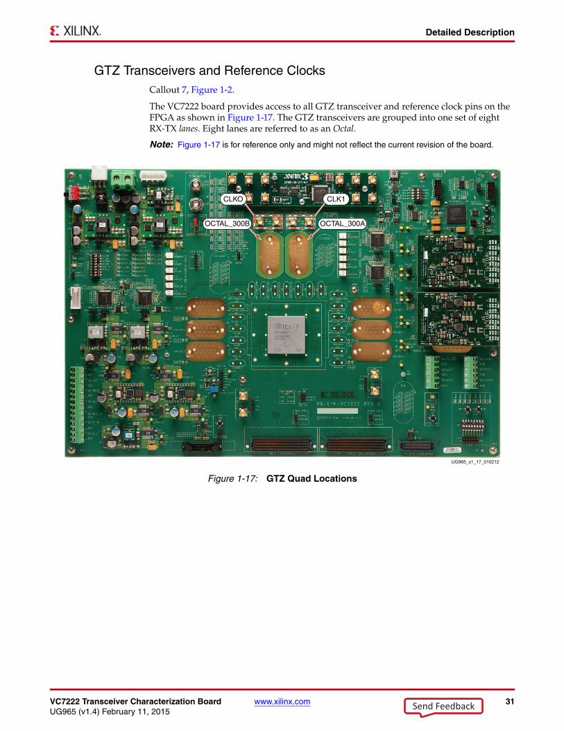
GTZ Transceivers and Reference ClocksCallout 7, Figure 1-2.
The VC7222 board provides access to all GTZ transceiver and reference clock pins on the FPGA as shown in Figure 1-17. The GTZ transceivers are grouped into one set of eight RX-TX lanes. Eight lanes are referred to as an Octal.
Note: Figure 1-17 is for reference only and might not reflect the current revision of the board.X-Ref Target - Figure 1-17
Figure 1-17: GTZ Quad Locations
UG965_c1_17_010212
OCTAL_300B OCTAL_300A
CLKO CLK1
Send Feedback
32 www.xilinx.com VC7222 Transceiver Characterization BoardUG965 (v1.4) February 11, 2015
Chapter 1: VC7222 Board Features and Operation
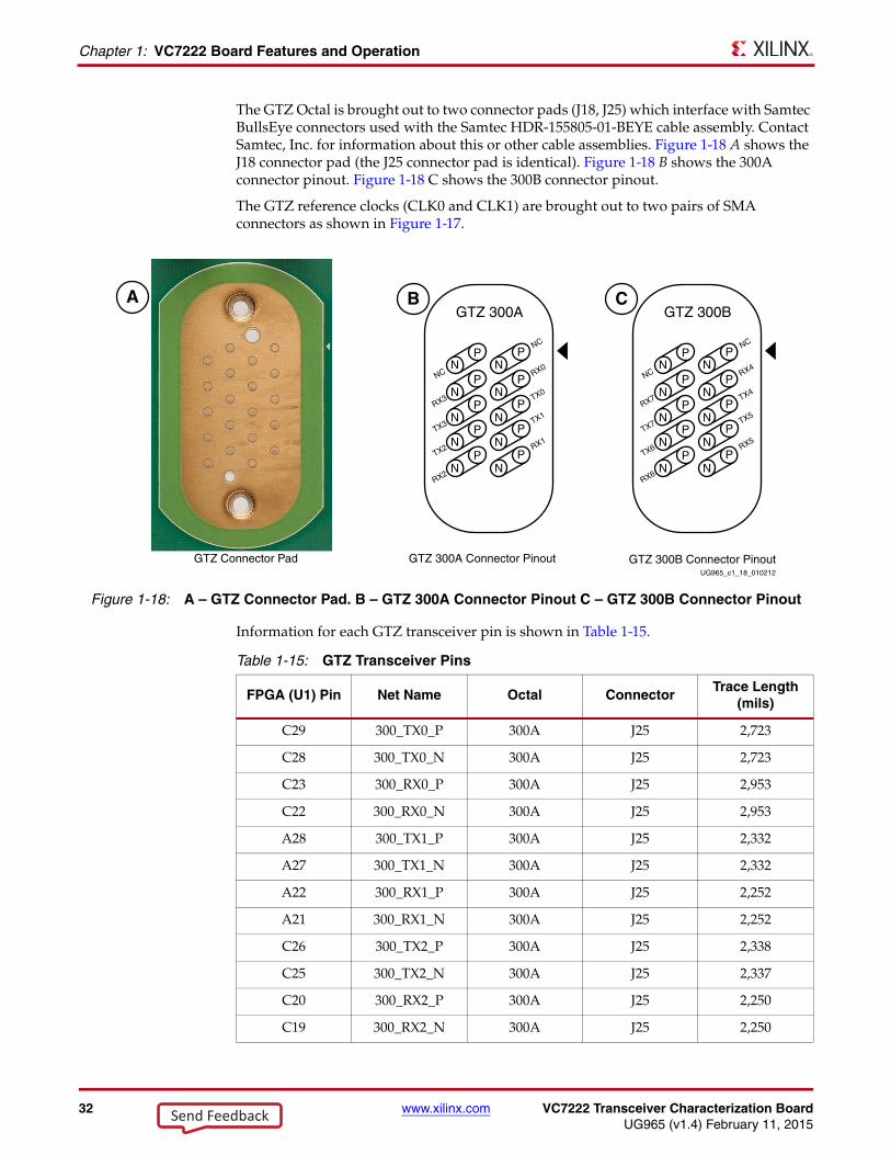
The GTZ Octal is brought out to two connector pads (J18, J25) which interface with Samtec BullsEye connectors used with the Samtec HDR-155805-01-BEYE cable assembly. Contact Samtec, Inc. for information about this or other cable assemblies. Figure 1-18 A shows the J18 connector pad (the J25 connector pad is identical). Figure 1-18 B shows the 300A connector pinout. Figure 1-18 C shows the 300B connector pinout.
The GTZ reference clocks (CLK0 and CLK1) are brought out to two pairs of SMA connectors as shown in Figure 1-17.
Information for each GTZ transceiver pin is shown in Table 1-15.
X-Ref Target - Figure 1-18
Figure 1-18: A – GTZ Connector Pad. B – GTZ 300A Connector Pinout C – GTZ 300B Connector Pinout
GTZ 300A Connector Pinout
A
GTZ Connector PadUG965_c1_18_010212
GTZ 300B Connector Pinout
CGTZ 300B
N
N
N
N
N
P
P
P
P
P
N
N
N
N
NP
P
P
P
P
RX6
TX6
TX5
RX5TX7
NC
RX4
TX4
NC
RX7
BGTZ 300A
N
N
N
N
N
P
P
P
P
P
N
N
N
N
NP
P
P
P
P
RX2
TX2
TX1
RX1TX3
NC
RX0
TX0
NC
RX3
Table 1-15: GTZ Transceiver Pins
FPGA (U1) Pin Net Name Octal ConnectorTrace Length
(mils)
C29 300_TX0_P 300A J25 2,723
C28 300_TX0_N 300A J25 2,723
C23 300_RX0_P 300A J25 2,953
C22 300_RX0_N 300A J25 2,953
A28 300_TX1_P 300A J25 2,332
A27 300_TX1_N 300A J25 2,332
A22 300_RX1_P 300A J25 2,252
A21 300_RX1_N 300A J25 2,252
C26 300_TX2_P 300A J25 2,338
C25 300_TX2_N 300A J25 2,337
C20 300_RX2_P 300A J25 2,250
C19 300_RX2_N 300A J25 2,250
Send Feedback

VC7222 Transceiver Characterization Board www.xilinx.com 33UG965 (v1.4) February 11, 2015
Detailed Description
Information for each GTZ transceiver clock input is shown in Table 1-16.
A25 300_TX3_P 300A J25 2,540
A24 300_TX3_N 300A J25 2,540
A19 300_RX3_P 300A J25 2,696
A18 300_RX3_N 300A J25 2,696
C17 300_TX4_P 300B J18 2,738
C16 300_TX4_N 300B J18 2,737
C11 300_RX4_P 300B J18 2,776
C10 300_RX4_N 300B J18 2,776
A16 300_TX5_P 300B J18 2,412
A15 300_TX5_N 300B J18 2,412
A10 300_RX5_P 300B J18 2,181
A9 300_RX5_N 300B J18 2,181
C14 300_TX6_P 300B J18 2,646
C13 300_TX6_N 300B J18 2,645
C8 300_RX6_P 300B J18 2,311
C7 300_RX6_N 300B J18 2,311
A13 300_TX7_P 300B J18 2,844
A12 300_TX7_N 300B J18 2,844
A7 300_RX7_P 300B J18 2,839
A6 300_RX7_N 300B J18 2,839
Table 1-16: GTZ Transceiver Reference Clock Inputs
FPGA (U1) Pin Net Name SMA Connector
E17 300_REFCLK0_P J57
E16 300_REFCLK0_N J56
E21 300_REFCLK1_P J46
E20 300_REFCLK1_N J47
Table 1-15: GTZ Transceiver Pins (Cont’d)
FPGA (U1) Pin Net Name Octal ConnectorTrace Length
(mils)
Send Feedback

34 www.xilinx.com VC7222 Transceiver Characterization BoardUG965 (v1.4) February 11, 2015
Chapter 1: VC7222 Board Features and Operation
USB-to-UART BridgeCallout 28, Figure 1-2.
A USB-to-UART bridge (U34, Silicon Laboratories CP2103) is provided for serial communication between a host computer and the FPGA over a USB cable. The USB connector on the board is a mini-B receptacle (J79) and its pinout is shown in Table 1-17.
The CP2103 supports an IO voltage range of 1.8V to 3.3V. Xilinx UART IP is expected to be implemented in the FPGA fabric. The FPGA supports the USB-to-UART bridge using four signal pins:
• Transmit (TX)
• Receive (RX)
• Request to Send (RTS)
• Clear to Send (CTS)
Connections of these signals between the FPGA and the CP2103 are listed in Table 1-18.
The bridge device also provides as many as 4 GPIO signals that can be defined by the user for status and control information (Table 1-19).
Table 1-17: USB Mini-B Receptacle Pin Assignments and Signals
J79 Pin Signal Name Description
1 VBUS+5V into the CP2103 USB-to-UART bridge at U34.Used to sense USB network connection.
2 USB_DATA_N Bidirectional differential serial data (N-side).
3 USB_DATA_P Bidirectional differential serial data (P-side).
4 GROUND Signal ground.
Table 1-18: FPGA to UART Connections
FPGA (U1) SchematicNet Name
Device (U34)
Pin Function Direction IOSTANDARD Pin Function Direction
AG11 RTS Output LVCMOS18 USB_CTS_I_B 22 CTS Input
AL9 CTS Input LVCMOS18 USB_RTS_0_B 23 RTS Output
AL10 TX Output LVCMOS18 USB_RXD_I 24 RXD Input
AK10 RX Input LVCMOS18 USB_TXD_0 25 TXD Output
Table 1-19: CP2103 USB-to-UART Bridge User GPIO
FPGA (U1) SchematicNet Name
Device (U34)
Pin Function Direction IOSTANDARD Pin Function Direction
AD10 SelectIO In/Out LVCMOS18 USB_GPIO_0 19 GPIO In/Out
AC8 SelectIO In/Out LVCMOS18 USB_GPIO_1 18 GPIO In/Out
AD8 SelectIO In/Out LVCMOS18 USB_GPIO_2 17 GPIO In/Out
AK11 SelectIO In/Out LVCMOS18 USB_GPIO_3 16 GPIO In/Out
Send Feedback

VC7222 Transceiver Characterization Board www.xilinx.com 35UG965 (v1.4) February 11, 2015
Detailed Description
A royalty-free software driver named Virtual COM Port (VCP) is available from Silicon Laboratories. This driver permits the CP2103 USB-to-UART bridge to appear as a COM port to the host computer communications application software (for example, HyperTerminal or TeraTerm). The VCP driver must be installed on the host computer prior to establishing communications with the VC7222 board.
FPGA Mezzanine Card HPC InterfaceCallout 34 and 35, Figure 1-2.
The VC7222 board features two high pin count (HPC) connectors as defined by the VITA 57.1 FPGA Mezzanine card (FMC) specification. The FMC HPC connector is a 10 x 40 position socket. See Appendix B, VITA 57.1 FMC Connector Pinouts for a cross-reference of signal names to pin coordinates.
FMC1 HPC connector JA2 provides connectivity for:
• 34 differential user defined pairs:
• 34 LA pairs
• 4 differential clocks
FMC2 HPC connector JA3 provides connectivity for:
• 57 differential user defined pairs:
• 34 LA pairs
• 12 HA pairs
• 11 HB pairs
• 2 differential clocks
Note: The VADJ voltage on the three FMC HPC connectors tracks VCCO_HP.
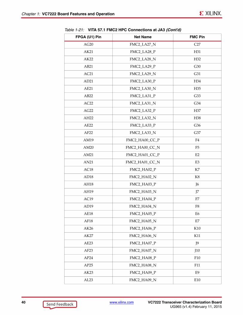
The FMC HPC connectors on the VC7222 board are identified as FMC1 at JA2 and FMC2 at JA3. The connections for each of these connectors are listed in Table 1-20 and Table 1-21, respectively.
Table 1-20: VITA 57.1 FMC1 HPC Connections at JA2
FPGA (U1) Pin Net Name FMC Pin
AK2 FMC1_CLK0_M2C_P H4
AL2 FMC1_CLK0_M2C_N H5
AJ15 FMC1_CLK1_M2C_P G2
AK15 FMC1_CLK1_M2C_N G3
AK3 FMC1_CLK2_BIDIR_P(1) K4
AL3 FMC1_CLK2_BIDIR_N(1) K5
AL15 FMC1_CLK3_BIDIR_P J2
AL14 FMC1_CLK3_BIDIR_N J3
AJ5 FMC1_LA00_CC_P(1) G6
AK5 FMC1_LA00_CC_N G7
AJ4 FMC1_LA01_CC_P D8
Send Feedback

36 www.xilinx.com VC7222 Transceiver Characterization BoardUG965 (v1.4) February 11, 2015
Chapter 1: VC7222 Board Features and Operation
AJ3 FMC1_LA01_CC_N D9
AG6 FMC1_LA02_P H7
AG5 FMC1_LA02_N H8
AH6 FMC1_LA03_P G9
AJ6 FMC1_LA03_N G10
AG7 FMC1_LA04_P H10
AH7 FMC1_LA04_N H11
AE7 FMC1_LA05_P D11
AF7 FMC1_LA05_N D12
AK7 FMC1_LA06_P C10
AK6 FMC1_LA06_N C11
AF4 FMC1_LA07_P H13
AG4 FMC1_LA07_N H14
AH4 FMC1_LA08_P G12
AH3 FMC1_LA08_N G13
AG2 FMC1_LA09_P D14
AH2 FMC1_LA09_N D15
AM2 FMC1_LA10_P C14
AN2 FMC1_LA10_N C15
AM1 FMC1_LA11_P H16
AN1 FMC1_LA11_N H17
AJ1 FMC1_LA12_P G15
AK1 FMC1_LA12_N G16
AN3 FMC1_LA13_P D17
AP3 FMC1_LA13_N D18
AM6 FMC1_LA14_P C18
AM5 FMC1_LA14_N C19
AL7 FMC1_LA15_P H19
AM7 FMC1_LA15_N H20
AM4 FMC1_LA16_P G18
AN4 FMC1_LA16_N G19
AM16 FMC1_LA17_CC_P D20
AM15 FMC1_LA17_CC_N D21
Table 1-20: VITA 57.1 FMC1 HPC Connections at JA2 (Cont’d)
FPGA (U1) Pin Net Name FMC Pin
Send Feedback

VC7222 Transceiver Characterization Board www.xilinx.com 37UG965 (v1.4) February 11, 2015
Detailed Description
AM14 FMC1_LA18_CC_P C22
AN14 FMC1_LA18_CC_N C23
AB17 FMC1_LA19_P H22
AC17 FMC1_LA19_N H23
AG17 FMC1_LA20_P G21
AH17 FMC1_LA20_N G22
AD16 FMC1_LA21_P H25
AE16 FMC1_LA21_N H26
AB16 FMC1_LA22_P G24
AC16 FMC1_LA22_N G25
AE17 FMC1_LA23_P D23
AF17 FMC1_LA23_N D24
AG16 FMC1_LA24_P H28
AH16 FMC1_LA24_N H29
AK17 FMC1_LA25_P G27
AL17 FMC1_LA25_N G28
AN16 FMC1_LA26_P D26
AP16 FMC1_LA26_N D27
AM17 FMC1_LA27_P C26
AN17 FMC1_LA27_N C27
AP15 FMC1_LA28_P H31
AP14 FMC1_LA28_N H32
AJ16 FMC1_LA29_P G30
AK16 FMC1_LA29_N G31
AD15 FMC1_LA30_P H34
AE15 FMC1_LA30_N H35
AK13 FMC1_LA31_P G33
AL13 FMC1_LA31_N G34
AF15 FMC1_LA32_P H37
AG15 FMC1_LA32_N H38
AH14 FMC1_LA33_P G36
Table 1-20: VITA 57.1 FMC1 HPC Connections at JA2 (Cont’d)
FPGA (U1) Pin Net Name FMC Pin
Send Feedback

38 www.xilinx.com VC7222 Transceiver Characterization BoardUG965 (v1.4) February 11, 2015
Chapter 1: VC7222 Board Features and Operation
AJ14 FMC1_LA33_N G37
AP1 FMC1_PRSNT_M2C_L H2
Notes: 1. This signal is connected to additional components and is not recommended for critical signals. See the
VC7222 schematic for additional information.
Table 1-21: VITA 57.1 FMC2 HPC Connections at JA3
FPGA (U1) Pin Net Name FMC Pin
AH31 FMC2_CLK0_M2C_P H4(1)
AJ31 FMC2_CLK0_M2C_N H5(1)
AK33 FMC2_CLK1_M2C_P G2
AL33 FMC2_CLK1_M2C_N G3
AK32 FMC2_LA00_CC_P G6(1)
AL32 FMC2_LA00_CC_N G7(1)
AK30 FMC2_LA01_CC_P D8
AK31 FMC2_LA01_CC_N D9
AE28 FMC2_LA02_P H7
AF28 FMC2_LA02_N H8
AJ29 FMC2_LA03_P G9
AJ30 FMC2_LA03_N G10
AF29 FMC2_LA04_P H10
AG29 FMC2_LA04_N H11
AH28 FMC2_LA05_P D11
AH29 FMC2_LA05_N D12
AJ28 FMC2_LA06_P C10
AK28 FMC2_LA06_N C11
AL28 FMC2_LA07_P H13
AL29 FMC2_LA07_N H14
AF30 FMC2_LA08_P G12
AG30 FMC2_LA08_N G13
AG31 FMC2_LA09_P D14
AG32 FMC2_LA09_N D15
AH32 FMC2_LA10_P C14(1)
AH33 FMC2_LA10_N C15
Table 1-20: VITA 57.1 FMC1 HPC Connections at JA2 (Cont’d)
FPGA (U1) Pin Net Name FMC Pin
Send Feedback
VC7222 Transceiver Characterization Board www.xilinx.com 39UG965 (v1.4) February 11, 2015
Detailed Description
AG34 FMC2_LA11_P H16
AH34 FMC2_LA11_N H17
AM32 FMC2_LA12_P G15(1)
AN32 FMC2_LA12_N G16
AL34 FMC2_LA13_P D17
AM34 FMC2_LA13_N D18
AJ33 FMC2_LA14_P C18
AJ34 FMC2_LA14_N C19
AN33 FMC2_LA15_P H19
AP33 FMC2_LA15_N H20
AM29 FMC2_LA16_P G18
AN29 FMC2_LA16_N G19
AJ20 FMC2_LA17_CC_P D20
AK20 FMC2_LA17_CC_N D21
AA20 FMC2_LA18_CC_P C22
AB20 FMC2_LA18_CC_N C23
AF19 FMC2_LA19_P H22
AG19 FMC2_LA19_N H23
AK18 FMC2_LA20_P G21
AL18 FMC2_LA20_N G22
AP20 FMC2_LA21_P H25
AP21 FMC2_LA21_N H26
AN19 FMC2_LA22_P G24
AP19 FMC2_LA22_N G25
AN18 FMC2_LA23_P D23
AP18 FMC2_LA23_N D24
AJ18 FMC2_LA24_P H28
AJ19 FMC2_LA24_N H29
AD20 FMC2_LA25_P G27
AE20 FMC2_LA25_N G28
AH21 FMC2_LA26_P D26
AJ21 FMC2_LA26_N D27
AF20 FMC2_LA27_P C26
Table 1-21: VITA 57.1 FMC2 HPC Connections at JA3 (Cont’d)
FPGA (U1) Pin Net Name FMC Pin
Send Feedback
40 www.xilinx.com VC7222 Transceiver Characterization BoardUG965 (v1.4) February 11, 2015
Chapter 1: VC7222 Board Features and Operation
AG20 FMC2_LA27_N C27
AK21 FMC2_LA28_P H31
AK22 FMC2_LA28_N H32
AB21 FMC2_LA29_P G30
AC21 FMC2_LA29_N G31
AD21 FMC2_LA30_P H34
AE21 FMC2_LA30_N H35
AB22 FMC2_LA31_P G33
AC22 FMC2_LA31_N G34
AG22 FMC2_LA32_P H37
AH22 FMC2_LA32_N H38
AE22 FMC2_LA33_P G36
AF22 FMC2_LA33_N G37
AM19 FMC2_HA00_CC_P F4
AM20 FMC2_HA00_CC_N F5
AM21 FMC2_HA01_CC_P E2
AN21 FMC2_HA01_CC_N E3
AC18 FMC2_HA02_P K7
AD18 FMC2_HA02_N K8
AH18 FMC2_HA03_P J6
AH19 FMC2_HA03_N J7
AC19 FMC2_HA04_P F7
AD19 FMC2_HA04_N F8
AE18 FMC2_HA05_P E6
AF18 FMC2_HA05_N E7
AK26 FMC2_HA06_P K10
AK27 FMC2_HA06_N K11
AE23 FMC2_HA07_P J9
AF23 FMC2_HA07_N J10
AP24 FMC2_HA08_P F10
AP25 FMC2_HA08_N F11
AK23 FMC2_HA09_P E9
AL23 FMC2_HA09_N E10
Table 1-21: VITA 57.1 FMC2 HPC Connections at JA3 (Cont’d)
FPGA (U1) Pin Net Name FMC Pin
Send Feedback

VC7222 Transceiver Characterization Board www.xilinx.com 41UG965 (v1.4) February 11, 2015
Detailed Description
AN23 FMC2_HA10_P K13
AP23 FMC2_HA10_N K14
AL19 FMC2_HA17_CC_P K16
AL20 FMC2_HA17_CC_N K17
AH24 FMC2_HB00_CC_P K25
AJ24 FMC2_HB00_CC_N K26
AC23 FMC2_HB01_P J24
AD23 FMC2_HB01_N J25
AD24 FMC2_HB02_P F22
AD25 FMC2_HB02_N F23
AB24 FMC2_HB03_P E21
AC24 FMC2_HB03_N E22
AM27 FMC2_HB04_P F25
AN27 FMC2_HB04_N F26
AL30 FMC2_HB05_P E24(1)
AM30 FMC2_HB05_N E25
AJ25 FMC2_HB06_CC_P K28
AK25 FMC2_HB06_CC_N K29
AP29 FMC2_HB07_P J27
AP30 FMC2_HB07_N J28
AM31 FMC2_HB08_P F28
AN31 FMC2_HB08_N F29
AN28 FMC2_HB09_P E27
AP28 FMC2_HB09_N E28
AG25 FMC2_HB17_CC_P K37
AG26 FMC2_HB17_CC_N K38
AN34 FMC2_PRSNT_M2C_L H2
Notes: 1. This signal is connected to additional components and is not recommended for critical signals. See the
VC7222 schematic for additional information.
Table 1-21: VITA 57.1 FMC2 HPC Connections at JA3 (Cont’d)
FPGA (U1) Pin Net Name FMC Pin
Send Feedback

42 www.xilinx.com VC7222 Transceiver Characterization BoardUG965 (v1.4) February 11, 2015
Chapter 1: VC7222 Board Features and Operation
XADCCallout 37, Figure 1-2.
The 7 series FPGAs provide an Analog Front End (XADC) block. The XADC block includes a dual 12-bit, 1 MSPS Analog-to-Digital Convertor (ADC) and on-chip sensors. See 7 Series FPGAs and Zynq-7000 All Programmable SoC XADC Dual 12-Bit 1 MSPS Analog-to-Digital Converter User Guide (UG480) [Ref 1] for details on the capabilities of the analog front end.
The VC7222 board provides two options for providing power (VCCADC) to the analog circuitry in the XADC. Either option can be selected by placing a shunt in one of two positions on the 3-pin VCCADC SELECT header, J141 (callout 31, Figure 1-2):
• Pins 1-2 (VCCAUX): In this configuration VCCADC is provided from VCCAUX through a low pass filter network.
• Pin 2-3 (REG): In this configuration VCCADC is provided by an onboard regulator, U43 (Analog Devices P/N ADP123AUJZ-R7). The output voltage of the regulator VCCADC can be adjusted using the potentiometer R233.
In addition, the VC7222 board provides two options for providing the reference voltage for the analog-to-digital converter. Either option can be selected by placing a shunt in one of two positions on the 3-pin VREF SEL header J142 (callout 31, Figure 1-2):
• Pins 1-2 (REG): In this configuration the ADC reference voltage is provided by an onboard, low-temperature coefficient 1.25V reference, U45 (Texas Instruments P/N REF3012AIDBZT)
• Pin 2-3 (AGND): In this configuration the VREFP on XADC is connected to analog ground and the ADC uses an on-chip reference.
I2C Bus ManagementThe I2C bus is controlled through U39, an 8-channel I2C-bus multiplexer (NXP Semiconductor PCA9547). The FPGA communicates with the multiplexer through I2C data and clock signals mapped to FPGA pins AG24 and AF24, respectively. The I2C idcode for the PCA9547 device is 0x70. The bus hosts four components:
• SuperClock-2 module
• 7 series GTH transceiver power supply module
• 7 series GTZ transceiver power supply module
• FMC1
• FMC2
An I2C component can be accessed by selecting the appropriate channel through the control register of the MUX as shown in Table 1-22.
Table 1-22: I2C Channel Assignments
U39 Channel I2C Component
0 SuperClock-2 module
1 7 series GTH transceiver power supply module
2 FMC1
3 FMC2
4 7 series GTZ transceiver power supply module
Send Feedback
VC7222 Transceiver Characterization Board www.xilinx.com 43UG965 (v1.4) February 11, 2015
Appendix A
Default Jumper and Switch Settings
Table A-1 lists the jumpers that must be installed on the VC7222 board for proper operation. These jumpers must be installed except where specifically noted in this user guide.
Note: Any jumper not listed in Table A-1 should be left open for normal operation.
DIP switch SW10 enables the supply of onboard core power to the FPGA. For normal operation positions 1 through 6 must be set to the ON position as shown in Figure A-1.
Table A-1: Default Jumper Settings
Reference Designator Name Board Location Jumper Comments
J4 UTIL_3V3 Upper Left AFX (1-2)
J184 UTIL_2V5 Upper Left AFX (1-2)
J24 UTIL_5V0 Upper Left AFX (1-2)
J66 PMBUS CTRL Center Left GND (2-3)
J48 Center Left POR (1-2)
J49 Center Left POR (1-2)
J50 Upper Right POR (1-2)
J68 Center Right POR (1-2)
J141 VCCADC SELECT Lower Left VCCAUX (1-2)
J142 VREF SEL Lower Left REG (1-2)
J23 SPI LVL TRNS INH Upper Right Installed
J8 SPI LVL TRNS INH Center Right Installed
J195 VTT_HP SOURCE Center Right GND (1-2) Red 20A jumper
X-Ref Target - Figure A-1
Figure A-1: Default Switch Settings
SW10
12
34
5
NCNCVCCO_0VCCO_HPVCCAUX_IO
ON
67
8
VCCBRAMVCCAUXVCCINT
DIS
AB
LED
UG965_aA_01_121912
Send Feedback

44 www.xilinx.com VC7222 Transceiver Characterization BoardUG965 (v1.4) February 11, 2015
Appendix A: Default Jumper and Switch Settings
Send Feedback

VC7222 Transceiver Characterization Board www.xilinx.com 45UG965 (v1.4) February 11, 2015
Appendix B
VITA 57.1 FMC Connector Pinouts
Figure B-1 provides a cross-reference of signal names to pin coordinates for the VITA 57.1 FMC HPC connector.
X-Ref Target - Figure B-1
Figure B-1: FMC HPC Connector Pinout
UG957_aB_01_070313
123456789
10111213141516171819202122232425262728293031323334353637383940
VREF_B_M2CGNDGND
CLK2_M2C_PCLK2_M2C_N
GNDHA02_PHA02_N
GNDHA06_PHA06_N
GNDHA10_PHA10_N
GNDHA17_P_CCHA17_N_CC
GNDHA21_PHA21_N
GNDHA23_PHA23_N
GNDHB00_P_CCHB00_N_CC
GNDHB06_P_CCHB06_N_CC
GNDHB10_PHB10_N
GNDHB14_PHB14_N
GNDHB17_P_CCHB17_N_CC
GNDVIO_B_M2C
GNDCLK3_M2C_PCLK3_M2C_N
GNDGND
HA03_PHA03_N
GNDHA07_PHA07_N
GNDHA11_PHA11_N
GNDHA14_PHA14_N
GNDHA18_PHA18_N
GNDHA22_PHA22_N
GNDHB01_PHB01_N
GNDHB07_PHB07_N
GNDHB11_PHB11_N
GNDHB15_PHB15_N
GNDHB18_PHB18_N
GNDVIO_B_M2C
GND
VREF_A_M2CPRSNT_M2C_L
GNDCLK0_M2C_PCLK0_M2C_N
GNDLA02_PLA02_N
GNDLA04_PLA04_N
GNDLA07_PLA07_N
GNDLA11_PLA11_N
GNDLA15_PLA15_N
GNDLA19_PLA19_N
GNDLA21_PLA21_N
GNDLA24_PLA24_N
GNDLA28_PLA28_N
GNDLA30_PLA30_N
GNDLA32_PLA32_N
GNDVADJ
GNDDP1_M2C_PDP1_M2C_N
GNDGND
DP2_M2C_PDP2_M2C_N
GNDGND
DP3_M2C_PDP3_M2C_N
GNDGND
DP4_M2C_PDP4_M2C_N
GNDGND
DP5_M2C_PDP5_M2C_N
GNDGND
DP1_C2M_PDP1_C2M_N
GNDGND
DP2_C2M_PDP2_C2M_N
GNDGND
DP3_C2M_PDP3_C2M_N
GNDGND
DP4_C2M_PDP4_C2M_N
GNDGND
DP5_C2M_PDP5_C2M_N
GND
RES1GNDGND
DP9_M2C_PDP9_M2C_N
GNDGND
DP8_M2C_PDP8_M2C_N
GNDGND
DP7_M2C_PDP7_M2C_N
GNDGND
DP6_M2C_PDP6_M2C_N
GNDGND
GBTCLK1_M2C_PGBTCLK1_M2C_N
GNDGND
DP9_C2M_PDP9_C2M_N
GNDGND
DP8_C2M_PDP8_C2M_N
GNDGND
DP7_C2M_PDP7_C2M_N
GNDGND
DP6_C2M_PDP6_C2M_N
GNDGNDRES0
GNDDP0_C2M_PDP0_C2M_N
GNDGND
DP0_M2C_PDP0_M2C_N
GNDGND
LA06_PLA06_N
GNDGND
LA10_PLA10_N
GNDGND
LA14_PLA14_N
GNDGND
LA18_P_CCLA18_N_CC
GNDGND
LA27_PLA27_N
GNDGNDSCLSDAGNDGNDGA0
12P0VGND
12P0VGND3P3VGND
PG_C2MGNDGND
GBTCLK0_M2C_PGBTCLK0_M2C_N
GNDGND
LA01_P_CCLA01_N_CC
GNDLA05_PLA05_N
GNDLA09_PLA09_N
GNDLA13_PLA13_N
GNDLA17_P_CCLA17_N_CC
GNDLA23_PLA23_N
GNDLA26_PLA26_N
GNDTCKTDITDO
3P3VAUXTMS
TRST_LGA13P3VGND3P3VGND3P3V
GNDHA01_P_CCHA01_N_CC
GNDGND
HA05_PHA05_N
GNDHA09_PHA09_N
GNDHA13_PHA13_N
GNDHA16_PHA16_N
GNDHA20_PHA20_N
GNDHB03_PHB03_N
GNDHB05_PHB05_N
GNDHB09_PHB09_N
GNDHB13_PHB13_N
GNDHB19_PHB19_N
GNDHB21_PHB21_N
GNDVADJGND
PG_M2CGNDGND
HA00_P_CCHA00_N_CC
GNDHA04_PHA04_N
GNDHA08_PHA08_N
GNDHA12_PHA12_N
GNDHA15_PHA15_N
GNDHA19_PHA19_N
GNDHB02_PHB02_N
GNDHB04_PHB04_N
GNDHB08_PHB08_N
GNDHB12_PHB12_N
GNDHB16_PHB16_N
GNDHB20_PHB20_N
GNDVADJ
GNDCLK1_M2C_PCLK1_M2C_N
GNDGND
LA00_P_CCLA00_N_CC
GNDLA03_PLA03_N
GNDLA08_PLA08_N
GNDLA12_PLA12_N
GNDLA16_PLA16_N
GNDLA20_PLA20_N
GNDLA22_PLA22_N
GNDLA25_PLA25_N
GNDLA29_PLA29_N
GNDLA31_PLA31_N
GNDLA33_PLA33_N
GNDVADJGND
K J H G F E D C B A
Send Feedback

46 www.xilinx.com VC7222 Transceiver Characterization BoardUG965 (v1.4) February 11, 2015
Appendix B: VITA 57.1 FMC Connector Pinouts
Send Feedback

VC7222 Transceiver Characterization Board www.xilinx.com 47UG965 (v1.4) February 11, 2015
Appendix C
Master Constraints File Listing
The VC7222 board master Xilinx design constraints (XDC) file template is provided for designs targeting the VC7222 Virtex®-7 FPGA GTH and GTZ Transceiver Characterization Board. Net names in the constraints listed below correlate with net names on the VC7222 board schematic. Users must identify the appropriate pins and replace the net names below with net names in the user RTL. See Vivado Design Suite User Guide: Using Constraints (UG903) [Ref 4] for more information.
VC7222 Board XDC Listing#FMC1set_property PACKAGE_PIN AP1 [get_ports FMC1_PRSNT_M2C_L]set_property IOSTANDARD LVCMOS18 [get_ports FMC1_PRSNT_M2C_L]set_property PACKAGE_PIN AK2 [get_ports FMC1_CLK0_M2C_P]set_property IOSTANDARD LVCMOS18 [get_ports FMC1_CLK0_M2C_P]set_property PACKAGE_PIN AL2 [get_ports FMC1_CLK0_M2C_N]set_property IOSTANDARD LVCMOS18 [get_ports FMC1_CLK0_M2C_N]set_property PACKAGE_PIN AJ15 [get_ports FMC1_CLK1_M2C_P]set_property IOSTANDARD LVCMOS18 [get_ports FMC1_CLK1_M2C_P]set_property PACKAGE_PIN AK15 [get_ports FMC1_CLK1_M2C_N]set_property IOSTANDARD LVCMOS18 [get_ports FMC1_CLK1_M2C_N]set_property PACKAGE_PIN AK3 [get_ports FMC1_CLK2_BIDIR_P]set_property IOSTANDARD LVDS [get_ports FMC1_CLK2_BIDIR_P]set_property PACKAGE_PIN AL3 [get_ports FMC1_CLK2_BIDIR_N]set_property IOSTANDARD LVDS [get_ports FMC1_CLK2_BIDIR_N]set_property PACKAGE_PIN AL15 [get_ports FMC1_CLK3_BIDIR_P]set_property IOSTANDARD LVCMOS18 [get_ports FMC1_CLK3_BIDIR_P]set_property PACKAGE_PIN AL14 [get_ports FMC1_CLK3_BIDIR_N]set_property IOSTANDARD LVCMOS18 [get_ports FMC1_CLK3_BIDIR_N]#FMC1 LAset_property PACKAGE_PIN AJ5 [get_ports FMC1_LA00_CC_P]set_property IOSTANDARD LVCMOS18 [get_ports FMC1_LA00_CC_P]set_property PACKAGE_PIN AK5 [get_ports FMC1_LA00_CC_N]set_property IOSTANDARD LVCMOS18 [get_ports FMC1_LA00_CC_N]set_property PACKAGE_PIN AJ4 [get_ports FMC1_LA01_CC_P]set_property IOSTANDARD LVCMOS18 [get_ports FMC1_LA01_CC_P]set_property PACKAGE_PIN AJ3 [get_ports FMC1_LA01_CC_N]set_property IOSTANDARD LVCMOS18 [get_ports FMC1_LA01_CC_N]set_property PACKAGE_PIN AG6 [get_ports FMC1_LA02_P]set_property IOSTANDARD LVCMOS18 [get_ports FMC1_LA02_P]set_property PACKAGE_PIN AG5 [get_ports FMC1_LA02_N]set_property IOSTANDARD LVCMOS18 [get_ports FMC1_LA02_N]set_property PACKAGE_PIN AH6 [get_ports FMC1_LA03_P]set_property IOSTANDARD LVCMOS18 [get_ports FMC1_LA03_P]set_property PACKAGE_PIN AJ6 [get_ports FMC1_LA03_N]
Send Feedback

48 www.xilinx.com VC7222 Transceiver Characterization BoardUG965 (v1.4) February 11, 2015
Appendix C: Master Constraints File Listing
set_property IOSTANDARD LVCMOS18 [get_ports FMC1_LA03_N]set_property PACKAGE_PIN AG7 [get_ports FMC1_LA04_P]set_property IOSTANDARD LVCMOS18 [get_ports FMC1_LA04_P]set_property PACKAGE_PIN AH7 [get_ports FMC1_LA04_N]set_property IOSTANDARD LVCMOS18 [get_ports FMC1_LA04_N]set_property PACKAGE_PIN AE7 [get_ports FMC1_LA05_P]set_property IOSTANDARD LVCMOS18 [get_ports FMC1_LA05_P]set_property PACKAGE_PIN AF7 [get_ports FMC1_LA05_N]set_property IOSTANDARD LVCMOS18 [get_ports FMC1_LA05_N]set_property PACKAGE_PIN AK7 [get_ports FMC1_LA06_P]set_property IOSTANDARD LVCMOS18 [get_ports FMC1_LA06_P]set_property PACKAGE_PIN AK6 [get_ports FMC1_LA06_N]set_property IOSTANDARD LVCMOS18 [get_ports FMC1_LA06_N]set_property PACKAGE_PIN AF4 [get_ports FMC1_LA07_P]set_property IOSTANDARD LVCMOS18 [get_ports FMC1_LA07_P]set_property PACKAGE_PIN AG4 [get_ports FMC1_LA07_N]set_property IOSTANDARD LVCMOS18 [get_ports FMC1_LA07_N]set_property PACKAGE_PIN AH4 [get_ports FMC1_LA08_P]set_property IOSTANDARD LVCMOS18 [get_ports FMC1_LA08_P]set_property PACKAGE_PIN AH3 [get_ports FMC1_LA08_N]set_property IOSTANDARD LVCMOS18 [get_ports FMC1_LA08_N]set_property PACKAGE_PIN AG2 [get_ports FMC1_LA09_P]set_property IOSTANDARD LVCMOS18 [get_ports FMC1_LA09_P]set_property PACKAGE_PIN AH2 [get_ports FMC1_LA09_N]set_property IOSTANDARD LVCMOS18 [get_ports FMC1_LA09_N]set_property PACKAGE_PIN AM2 [get_ports FMC1_LA10_P]set_property IOSTANDARD LVCMOS18 [get_ports FMC1_LA10_P]set_property PACKAGE_PIN AN2 [get_ports FMC1_LA10_N]set_property IOSTANDARD LVCMOS18 [get_ports FMC1_LA10_N]set_property PACKAGE_PIN AM1 [get_ports FMC1_LA11_P]set_property IOSTANDARD LVCMOS18 [get_ports FMC1_LA11_P]set_property PACKAGE_PIN AN1 [get_ports FMC1_LA11_N]set_property IOSTANDARD LVCMOS18 [get_ports FMC1_LA11_N]set_property PACKAGE_PIN AJ1 [get_ports FMC1_LA12_P]set_property IOSTANDARD LVCMOS18 [get_ports FMC1_LA12_P]set_property PACKAGE_PIN AK1 [get_ports FMC1_LA12_N]set_property IOSTANDARD LVCMOS18 [get_ports FMC1_LA12_N]set_property PACKAGE_PIN AN3 [get_ports FMC1_LA13_P]set_property IOSTANDARD LVCMOS18 [get_ports FMC1_LA13_P]set_property PACKAGE_PIN AP3 [get_ports FMC1_LA13_N]set_property IOSTANDARD LVCMOS18 [get_ports FMC1_LA13_N]set_property PACKAGE_PIN AM6 [get_ports FMC1_LA14_P]set_property IOSTANDARD LVCMOS18 [get_ports FMC1_LA14_P]set_property PACKAGE_PIN AM5 [get_ports FMC1_LA14_N]set_property IOSTANDARD LVCMOS18 [get_ports FMC1_LA14_N]set_property PACKAGE_PIN AL7 [get_ports FMC1_LA15_P]set_property IOSTANDARD LVCMOS18 [get_ports FMC1_LA15_P]set_property PACKAGE_PIN AM7 [get_ports FMC1_LA15_N]set_property IOSTANDARD LVCMOS18 [get_ports FMC1_LA15_N]set_property PACKAGE_PIN AM4 [get_ports FMC1_LA16_P]set_property IOSTANDARD LVCMOS18 [get_ports FMC1_LA16_P]set_property PACKAGE_PIN AN4 [get_ports FMC1_LA16_N]set_property IOSTANDARD LVCMOS18 [get_ports FMC1_LA16_N]set_property PACKAGE_PIN AM16 [get_ports FMC1_LA17_CC_P]set_property IOSTANDARD LVCMOS18 [get_ports FMC1_LA17_CC_P]set_property PACKAGE_PIN AM15 [get_ports FMC1_LA17_CC_N]set_property IOSTANDARD LVCMOS18 [get_ports FMC1_LA17_CC_N]set_property PACKAGE_PIN AM14 [get_ports FMC1_LA18_CC_P]set_property IOSTANDARD LVCMOS18 [get_ports FMC1_LA18_CC_P]
Send Feedback

VC7222 Transceiver Characterization Board www.xilinx.com 49UG965 (v1.4) February 11, 2015
VC7222 Board XDC Listing
set_property PACKAGE_PIN AN14 [get_ports FMC1_LA18_CC_N]set_property IOSTANDARD LVCMOS18 [get_ports FMC1_LA18_CC_N]set_property PACKAGE_PIN AB17 [get_ports FMC1_LA19_P]set_property IOSTANDARD LVCMOS18 [get_ports FMC1_LA19_P]set_property PACKAGE_PIN AC17 [get_ports FMC1_LA19_N]set_property IOSTANDARD LVCMOS18 [get_ports FMC1_LA19_N]set_property PACKAGE_PIN AG17 [get_ports FMC1_LA20_P]set_property IOSTANDARD LVCMOS18 [get_ports FMC1_LA20_P]set_property PACKAGE_PIN AH17 [get_ports FMC1_LA20_N]set_property IOSTANDARD LVCMOS18 [get_ports FMC1_LA20_N]set_property PACKAGE_PIN AD16 [get_ports FMC1_LA21_P]set_property IOSTANDARD LVCMOS18 [get_ports FMC1_LA21_P]set_property PACKAGE_PIN AE16 [get_ports FMC1_LA21_N]set_property IOSTANDARD LVCMOS18 [get_ports FMC1_LA21_N]set_property PACKAGE_PIN AB16 [get_ports FMC1_LA22_P]set_property IOSTANDARD LVCMOS18 [get_ports FMC1_LA22_P]set_property PACKAGE_PIN AC16 [get_ports FMC1_LA22_N]set_property IOSTANDARD LVCMOS18 [get_ports FMC1_LA22_N]set_property PACKAGE_PIN AE17 [get_ports FMC1_LA23_P]set_property IOSTANDARD LVCMOS18 [get_ports FMC1_LA23_P]set_property PACKAGE_PIN AF17 [get_ports FMC1_LA23_N]set_property IOSTANDARD LVCMOS18 [get_ports FMC1_LA23_N]set_property PACKAGE_PIN AG16 [get_ports FMC1_LA24_P]set_property IOSTANDARD LVCMOS18 [get_ports FMC1_LA24_P]set_property PACKAGE_PIN AH16 [get_ports FMC1_LA24_N]set_property IOSTANDARD LVCMOS18 [get_ports FMC1_LA24_N]set_property PACKAGE_PIN AK17 [get_ports FMC1_LA25_P]set_property IOSTANDARD LVCMOS18 [get_ports FMC1_LA25_P]set_property PACKAGE_PIN AL17 [get_ports FMC1_LA25_N]set_property IOSTANDARD LVCMOS18 [get_ports FMC1_LA25_N]set_property PACKAGE_PIN AN16 [get_ports FMC1_LA26_P]set_property IOSTANDARD LVCMOS18 [get_ports FMC1_LA26_P]set_property PACKAGE_PIN AP16 [get_ports FMC1_LA26_N]set_property IOSTANDARD LVCMOS18 [get_ports FMC1_LA26_N]set_property PACKAGE_PIN AM17 [get_ports FMC1_LA27_P]set_property IOSTANDARD LVCMOS18 [get_ports FMC1_LA27_P]set_property PACKAGE_PIN AN17 [get_ports FMC1_LA27_N]set_property IOSTANDARD LVCMOS18 [get_ports FMC1_LA27_N]set_property PACKAGE_PIN AP15 [get_ports FMC1_LA28_P]set_property IOSTANDARD LVCMOS18 [get_ports FMC1_LA28_P]set_property PACKAGE_PIN AP14 [get_ports FMC1_LA28_N]set_property IOSTANDARD LVCMOS18 [get_ports FMC1_LA28_N]set_property PACKAGE_PIN AJ16 [get_ports FMC1_LA29_P]set_property IOSTANDARD LVCMOS18 [get_ports FMC1_LA29_P]set_property PACKAGE_PIN AK16 [get_ports FMC1_LA29_N]set_property IOSTANDARD LVCMOS18 [get_ports FMC1_LA29_N]set_property PACKAGE_PIN AD15 [get_ports FMC1_LA30_P]set_property IOSTANDARD LVCMOS18 [get_ports FMC1_LA30_P]set_property PACKAGE_PIN AE15 [get_ports FMC1_LA30_N]set_property IOSTANDARD LVCMOS18 [get_ports FMC1_LA30_N]set_property PACKAGE_PIN AK13 [get_ports FMC1_LA31_P]set_property IOSTANDARD LVCMOS18 [get_ports FMC1_LA31_P]set_property PACKAGE_PIN AL13 [get_ports FMC1_LA31_N]set_property IOSTANDARD LVCMOS18 [get_ports FMC1_LA31_N]set_property PACKAGE_PIN AF15 [get_ports FMC1_LA32_P]set_property IOSTANDARD LVCMOS18 [get_ports FMC1_LA32_P]set_property PACKAGE_PIN AG15 [get_ports FMC1_LA32_N]set_property IOSTANDARD LVCMOS18 [get_ports FMC1_LA32_N]set_property PACKAGE_PIN AH14 [get_ports FMC1_LA33_P]
Send Feedback

50 www.xilinx.com VC7222 Transceiver Characterization BoardUG965 (v1.4) February 11, 2015
Appendix C: Master Constraints File Listing
set_property IOSTANDARD LVCMOS18 [get_ports FMC1_LA33_P]set_property PACKAGE_PIN AJ14 [get_ports FMC1_LA33_N]set_property IOSTANDARD LVCMOS18 [get_ports FMC1_LA33_N]#FMC2set_property PACKAGE_PIN AN34 [get_ports FMC2_PRSNT_M2C_L]set_property IOSTANDARD LVCMOS18 [get_ports FMC2_PRSNT_M2C_L]set_property PACKAGE_PIN AH31 [get_ports FMC2_CLK0_M2C_P]set_property IOSTANDARD LVCMOS18 [get_ports FMC2_CLK0_M2C_P]set_property PACKAGE_PIN AJ31 [get_ports IO_L11N_T1_SRCC_14]set_property IOSTANDARD LVCMOS18 [get_ports IO_L11N_T1_SRCC_14]set_property PACKAGE_PIN AK33 [get_ports FMC2_CLK1_M2C_P]set_property IOSTANDARD LVCMOS18 [get_ports FMC2_CLK1_M2C_P]set_property PACKAGE_PIN AL33 [get_ports FMC2_CLK1_M2C_N]set_property IOSTANDARD LVCMOS18 [get_ports FMC2_CLK1_M2C_N]#FMC2 LAset_property PACKAGE_PIN AK32 [get_ports FMC2_LA00_CC_P]set_property IOSTANDARD LVDS [get_ports FMC2_LA00_CC_P]set_property PACKAGE_PIN AL32 [get_ports FMC2_LA00_CC_N]set_property IOSTANDARD LVDS [get_ports FMC2_LA00_CC_N]set_property PACKAGE_PIN AK30 [get_ports FMC2_LA01_CC_P]set_property IOSTANDARD LVCMOS18 [get_ports FMC2_LA01_CC_P]set_property PACKAGE_PIN AK31 [get_ports FMC2_LA01_CC_N]set_property IOSTANDARD LVCMOS18 [get_ports FMC2_LA01_CC_N]set_property PACKAGE_PIN AE28 [get_ports FMC2_LA02_P]set_property IOSTANDARD LVCMOS18 [get_ports FMC2_LA02_P]set_property PACKAGE_PIN AF28 [get_ports FMC2_LA02_N]set_property IOSTANDARD LVCMOS18 [get_ports FMC2_LA02_N]set_property PACKAGE_PIN AJ29 [get_ports FMC2_LA03_P]set_property IOSTANDARD LVCMOS18 [get_ports FMC2_LA03_P]set_property PACKAGE_PIN AJ30 [get_ports FMC2_LA03_N]set_property IOSTANDARD LVCMOS18 [get_ports FMC2_LA03_N]set_property PACKAGE_PIN AF29 [get_ports FMC2_LA04_P]set_property IOSTANDARD LVCMOS18 [get_ports FMC2_LA04_P]set_property PACKAGE_PIN AG29 [get_ports FMC2_LA04_N]set_property IOSTANDARD LVCMOS18 [get_ports FMC2_LA04_N]set_property PACKAGE_PIN AH28 [get_ports FMC2_LA05_P]set_property IOSTANDARD LVCMOS18 [get_ports FMC2_LA05_P]set_property PACKAGE_PIN AH29 [get_ports FMC2_LA05_N]set_property IOSTANDARD LVCMOS18 [get_ports FMC2_LA05_N]set_property PACKAGE_PIN AJ28 [get_ports FMC2_LA06_P]set_property IOSTANDARD LVCMOS18 [get_ports FMC2_LA06_P]set_property PACKAGE_PIN AK28 [get_ports FMC2_LA06_N]set_property IOSTANDARD LVCMOS18 [get_ports FMC2_LA06_N]set_property PACKAGE_PIN AL28 [get_ports FMC2_LA07_P]set_property IOSTANDARD LVCMOS18 [get_ports FMC2_LA07_P]set_property PACKAGE_PIN AL29 [get_ports FMC2_LA07_N]set_property IOSTANDARD LVCMOS18 [get_ports FMC2_LA07_N]set_property PACKAGE_PIN AF30 [get_ports FMC2_LA08_P]set_property IOSTANDARD LVCMOS18 [get_ports FMC2_LA08_P]set_property PACKAGE_PIN AG30 [get_ports FMC2_LA08_N]set_property IOSTANDARD LVCMOS18 [get_ports FMC2_LA08_N]set_property PACKAGE_PIN AG31 [get_ports FMC2_LA09_P]set_property IOSTANDARD LVCMOS18 [get_ports FMC2_LA09_P]set_property PACKAGE_PIN AG32 [get_ports FMC2_LA09_N]set_property IOSTANDARD LVCMOS18 [get_ports FMC2_LA09_N]set_property PACKAGE_PIN AH32 [get_ports FMC2_LA10_N]set_property IOSTANDARD LVCMOS18 [get_ports FMC2_LA10_N]set_property PACKAGE_PIN AH33 [get_ports FMC2_LA10_N]set_property IOSTANDARD LVCMOS18 [get_ports FMC2_LA10_N]
Send Feedback

VC7222 Transceiver Characterization Board www.xilinx.com 51UG965 (v1.4) February 11, 2015
VC7222 Board XDC Listing
set_property PACKAGE_PIN AG34 [get_ports FMC2_LA11_P]set_property IOSTANDARD LVCMOS18 [get_ports FMC2_LA11_P]set_property PACKAGE_PIN AH34 [get_ports FMC2_LA11_N]set_property IOSTANDARD LVCMOS18 [get_ports FMC2_LA11_N]set_property PACKAGE_PIN AM32 [get_ports FMC2_LA12_P]set_property IOSTANDARD LVCMOS18 [get_ports FMC2_LA12_P]set_property PACKAGE_PIN AN32 [get_ports FMC2_LA12_N]set_property IOSTANDARD LVCMOS18 [get_ports FMC2_LA12_N]set_property PACKAGE_PIN AL34 [get_ports FMC2_LA13_P]set_property IOSTANDARD LVCMOS18 [get_ports FMC2_LA13_P]set_property PACKAGE_PIN AM34 [get_ports FMC2_LA13_N]set_property IOSTANDARD LVCMOS18 [get_ports FMC2_LA13_N]set_property PACKAGE_PIN AJ33 [get_ports FMC2_LA14_P]set_property IOSTANDARD LVCMOS18 [get_ports FMC2_LA14_P]set_property PACKAGE_PIN AJ34 [get_ports FMC2_LA14_N]set_property IOSTANDARD LVCMOS18 [get_ports FMC2_LA14_N]set_property PACKAGE_PIN AN33 [get_ports FMC2_LA15_P]set_property IOSTANDARD LVCMOS18 [get_ports FMC2_LA15_P]set_property PACKAGE_PIN AP33 [get_ports FMC2_LA15_N]set_property IOSTANDARD LVCMOS18 [get_ports FMC2_LA15_N]set_property PACKAGE_PIN AM29 [get_ports FMC2_LA16_P]set_property IOSTANDARD LVCMOS18 [get_ports FMC2_LA16_P]set_property PACKAGE_PIN AN29 [get_ports FMC2_LA16_N]set_property IOSTANDARD LVCMOS18 [get_ports FMC2_LA16_N]set_property PACKAGE_PIN AJ20 [get_ports FMC2_LA17_CC_P]set_property IOSTANDARD LVCMOS18 [get_ports FMC2_LA17_CC_P]set_property PACKAGE_PIN AK20 [get_ports FMC2_LA17_CC_N]set_property IOSTANDARD LVCMOS18 [get_ports FMC2_LA17_CC_N]set_property PACKAGE_PIN AA20 [get_ports FMC2_LA18_CC_P]set_property IOSTANDARD LVCMOS18 [get_ports FMC2_LA18_CC_P]set_property PACKAGE_PIN AB20 [get_ports FMC2_LA18_CC_N]set_property IOSTANDARD LVCMOS18 [get_ports FMC2_LA18_CC_N]set_property PACKAGE_PIN AF19 [get_ports FMC2_LA19_P]set_property IOSTANDARD LVCMOS18 [get_ports FMC2_LA19_P]set_property PACKAGE_PIN AG19 [get_ports FMC2_LA19_N]set_property IOSTANDARD LVCMOS18 [get_ports FMC2_LA19_N]set_property PACKAGE_PIN AK18 [get_ports FMC2_LA20_P]set_property IOSTANDARD LVCMOS18 [get_ports FMC2_LA20_P]set_property PACKAGE_PIN AL18 [get_ports FMC2_LA20_N]set_property IOSTANDARD LVCMOS18 [get_ports FMC2_LA20_N]set_property PACKAGE_PIN AP20 [get_ports FMC2_LA21_P]set_property IOSTANDARD LVCMOS18 [get_ports FMC2_LA21_P]set_property PACKAGE_PIN AP21 [get_ports FMC2_LA21_N]set_property IOSTANDARD LVCMOS18 [get_ports FMC2_LA21_N]set_property PACKAGE_PIN AN19 [get_ports FMC2_LA22_P]set_property IOSTANDARD LVCMOS18 [get_ports FMC2_LA22_P]set_property PACKAGE_PIN AP19 [get_ports FMC2_LA22_N]set_property IOSTANDARD LVCMOS18 [get_ports FMC2_LA22_N]set_property PACKAGE_PIN AN18 [get_ports FMC2_LA23_P]set_property IOSTANDARD LVCMOS18 [get_ports FMC2_LA23_P]set_property PACKAGE_PIN AP18 [get_ports FMC2_LA23_N]set_property IOSTANDARD LVCMOS18 [get_ports FMC2_LA23_N]set_property PACKAGE_PIN AJ18 [get_ports FMC2_LA24_P]set_property IOSTANDARD LVCMOS18 [get_ports FMC2_LA24_P]set_property PACKAGE_PIN AJ19 [get_ports FMC2_LA24_N]set_property IOSTANDARD LVCMOS18 [get_ports FMC2_LA24_N]set_property PACKAGE_PIN AD20 [get_ports FMC2_LA25_P]set_property IOSTANDARD LVCMOS18 [get_ports FMC2_LA25_P]set_property PACKAGE_PIN AE20 [get_ports FMC2_LA25_N]
Send Feedback

52 www.xilinx.com VC7222 Transceiver Characterization BoardUG965 (v1.4) February 11, 2015
Appendix C: Master Constraints File Listing
set_property IOSTANDARD LVCMOS18 [get_ports FMC2_LA25_N]set_property PACKAGE_PIN AH21 [get_ports FMC2_LA26_P]set_property IOSTANDARD LVCMOS18 [get_ports FMC2_LA26_P]set_property PACKAGE_PIN AJ21 [get_ports FMC2_LA26_N]set_property IOSTANDARD LVCMOS18 [get_ports FMC2_LA26_N]set_property PACKAGE_PIN AF20 [get_ports FMC2_LA27_P]set_property IOSTANDARD LVCMOS18 [get_ports FMC2_LA27_P]set_property PACKAGE_PIN AG20 [get_ports FMC2_LA27_N]set_property IOSTANDARD LVCMOS18 [get_ports FMC2_LA27_N]set_property PACKAGE_PIN AK21 [get_ports FMC2_LA28_P]set_property IOSTANDARD LVCMOS18 [get_ports FMC2_LA28_P]set_property PACKAGE_PIN AK22 [get_ports FMC2_LA28_N]set_property IOSTANDARD LVCMOS18 [get_ports FMC2_LA28_N]set_property PACKAGE_PIN AB21 [get_ports FMC2_LA29_P]set_property IOSTANDARD LVCMOS18 [get_ports FMC2_LA29_P]set_property PACKAGE_PIN AC21 [get_ports FMC2_LA29_N]set_property IOSTANDARD LVCMOS18 [get_ports FMC2_LA29_N]set_property PACKAGE_PIN AD21 [get_ports FMC2_LA30_P]set_property IOSTANDARD LVCMOS18 [get_ports FMC2_LA30_P]set_property PACKAGE_PIN AE21 [get_ports FMC2_LA30_N]set_property IOSTANDARD LVCMOS18 [get_ports FMC2_LA30_N]set_property PACKAGE_PIN AB22 [get_ports FMC2_LA31_P]set_property IOSTANDARD LVCMOS18 [get_ports FMC2_LA31_P]set_property PACKAGE_PIN AC22 [get_ports FMC2_LA31_N]set_property IOSTANDARD LVCMOS18 [get_ports FMC2_LA31_N]set_property PACKAGE_PIN AG22 [get_ports FMC2_LA32_P]set_property IOSTANDARD LVCMOS18 [get_ports FMC2_LA32_P]set_property PACKAGE_PIN AH22 [get_ports FMC2_LA32_N]set_property IOSTANDARD LVCMOS18 [get_ports FMC2_LA32_N]set_property PACKAGE_PIN AE22 [get_ports FMC2_LA33_P]set_property IOSTANDARD LVCMOS18 [get_ports FMC2_LA33_P]set_property PACKAGE_PIN AF22 [get_ports FMC2_LA33_N]set_property IOSTANDARD LVCMOS18 [get_ports FMC2_LA33_N]#FMC2 HAset_property PACKAGE_PIN AM19 [get_ports FMC2_HA00_CC_P]set_property IOSTANDARD LVCMOS18 [get_ports FMC2_HA00_CC_P]set_property PACKAGE_PIN AM20 [get_ports FMC2_HA00_CC_N]set_property IOSTANDARD LVCMOS18 [get_ports FMC2_HA00_CC_N]set_property PACKAGE_PIN AM21 [get_ports FMC2_HA01_CC_P]set_property IOSTANDARD LVCMOS18 [get_ports FMC2_HA01_CC_P]set_property PACKAGE_PIN AN21 [get_ports FMC2_HA01_CC_N]set_property IOSTANDARD LVCMOS18 [get_ports FMC2_HA01_CC_N]set_property PACKAGE_PIN AC18 [get_ports FMC2_HA02_P]set_property IOSTANDARD LVCMOS18 [get_ports FMC2_HA02_P]set_property PACKAGE_PIN AD18 [get_ports FMC2_HA02_N]set_property IOSTANDARD LVCMOS18 [get_ports FMC2_HA02_N]set_property PACKAGE_PIN AH18 [get_ports FMC2_HA03_P]set_property IOSTANDARD LVCMOS18 [get_ports FMC2_HA03_P]set_property PACKAGE_PIN AH19 [get_ports FMC2_HA03_N]set_property IOSTANDARD LVCMOS18 [get_ports FMC2_HA03_N]set_property PACKAGE_PIN AC19 [get_ports FMC2_HA04_P]set_property IOSTANDARD LVCMOS18 [get_ports FMC2_HA04_P]set_property PACKAGE_PIN AD19 [get_ports FMC2_HA04_N]set_property IOSTANDARD LVCMOS18 [get_ports FMC2_HA04_N]set_property PACKAGE_PIN AE18 [get_ports FMC2_HA05_P]set_property IOSTANDARD LVCMOS18 [get_ports FMC2_HA05_P]set_property PACKAGE_PIN AF18 [get_ports FMC2_HA05_N]set_property IOSTANDARD LVCMOS18 [get_ports FMC2_HA05_N]set_property PACKAGE_PIN AK26 [get_ports FMC2_HA06_P]
Send Feedback
VC7222 Transceiver Characterization Board www.xilinx.com 53UG965 (v1.4) February 11, 2015
VC7222 Board XDC Listing
set_property IOSTANDARD LVCMOS18 [get_ports FMC2_HA06_P]set_property PACKAGE_PIN AK27 [get_ports FMC2_HA06_N]set_property IOSTANDARD LVCMOS18 [get_ports FMC2_HA06_N]set_property PACKAGE_PIN AE23 [get_ports FMC2_HA07_P]set_property IOSTANDARD LVCMOS18 [get_ports FMC2_HA07_P]set_property PACKAGE_PIN AF23 [get_ports FMC2_HA07_N]set_property IOSTANDARD LVCMOS18 [get_ports FMC2_HA07_N]set_property PACKAGE_PIN AP24 [get_ports FMC2_HA08_P]set_property IOSTANDARD LVCMOS18 [get_ports FMC2_HA08_P]set_property PACKAGE_PIN AP25 [get_ports FMC2_HA08_N]set_property IOSTANDARD LVCMOS18 [get_ports FMC2_HA08_N]set_property PACKAGE_PIN AK23 [get_ports FMC2_HA09_P]set_property IOSTANDARD LVCMOS18 [get_ports FMC2_HA09_P]set_property PACKAGE_PIN AL23 [get_ports FMC2_HA09_N]set_property IOSTANDARD LVCMOS18 [get_ports FMC2_HA09_N]set_property PACKAGE_PIN AN23 [get_ports FMC2_HA10_P]set_property IOSTANDARD LVCMOS18 [get_ports FMC2_HA10_P]set_property PACKAGE_PIN AP23 [get_ports FMC2_HA10_N]set_property IOSTANDARD LVCMOS18 [get_ports FMC2_HA10_N]set_property PACKAGE_PIN AL19 [get_ports FMC2_HA17_CC_P]set_property IOSTANDARD LVCMOS18 [get_ports FMC2_HA17_CC_P]set_property PACKAGE_PIN AL20 [get_ports FMC2_HA17_CC_N]set_property IOSTANDARD LVCMOS18 [get_ports FMC2_HA17_CC_N]#FMC2 HBset_property PACKAGE_PIN AH24 [get_ports FMC2_HB00_CC_P]set_property IOSTANDARD LVCMOS18 [get_ports FMC2_HB00_CC_P]set_property PACKAGE_PIN AJ24 [get_ports FMC2_HB00_CC_N]set_property IOSTANDARD LVCMOS18 [get_ports FMC2_HB00_CC_N]set_property PACKAGE_PIN AC23 [get_ports FMC2_HB01_P]set_property IOSTANDARD LVCMOS18 [get_ports FMC2_HB01_P]set_property PACKAGE_PIN AD23 [get_ports FMC2_HB01_N]set_property IOSTANDARD LVCMOS18 [get_ports FMC2_HB01_N]set_property PACKAGE_PIN AD24 [get_ports FMC2_HB02_P]set_property IOSTANDARD LVCMOS18 [get_ports FMC2_HB02_P]set_property PACKAGE_PIN AD25 [get_ports FMC2_HB02_N]set_property IOSTANDARD LVCMOS18 [get_ports FMC2_HB02_N]set_property PACKAGE_PIN AB24 [get_ports FMC2_HB03_P]set_property IOSTANDARD LVCMOS18 [get_ports FMC2_HB03_P]set_property PACKAGE_PIN AC24 [get_ports FMC2_HB03_N]set_property IOSTANDARD LVCMOS18 [get_ports FMC2_HB03_N]set_property PACKAGE_PIN AM27 [get_ports FMC2_HB04_P]set_property IOSTANDARD LVCMOS18 [get_ports FMC2_HB04_P]set_property PACKAGE_PIN AN27 [get_ports FMC2_HB04_N]set_property IOSTANDARD LVCMOS18 [get_ports FMC2_HB04_N]set_property PACKAGE_PIN AL30 [get_ports FMC2_HB05_P]set_property IOSTANDARD LVCMOS18 [get_ports FMC2_HB05_P]set_property PACKAGE_PIN AM30 [get_ports FMC2_HB05_N]set_property IOSTANDARD LVCMOS18 [get_ports FMC2_HB05_N]set_property PACKAGE_PIN AJ25 [get_ports FMC2_HB06_CC_P]set_property IOSTANDARD LVCMOS18 [get_ports FMC2_HB06_CC_P]set_property PACKAGE_PIN AK25 [get_ports FMC2_HB06_CC_N]set_property IOSTANDARD LVCMOS18 [get_ports FMC2_HB06_CC_N]set_property PACKAGE_PIN AP29 [get_ports FMC2_HB07_P]set_property IOSTANDARD LVCMOS18 [get_ports FMC2_HB07_P]set_property PACKAGE_PIN AP30 [get_ports FMC2_HB07_N]set_property IOSTANDARD LVCMOS18 [get_ports FMC2_HB07_N]set_property PACKAGE_PIN AM31 [get_ports FMC2_HB08_P]set_property IOSTANDARD LVCMOS18 [get_ports FMC2_HB08_P]set_property PACKAGE_PIN AN31 [get_ports FMC2_HB08_N]
Send Feedback

54 www.xilinx.com VC7222 Transceiver Characterization BoardUG965 (v1.4) February 11, 2015
Appendix C: Master Constraints File Listing
set_property IOSTANDARD LVCMOS18 [get_ports FMC2_HB08_N]set_property PACKAGE_PIN AN28 [get_ports FMC2_HB09_P]set_property IOSTANDARD LVCMOS18 [get_ports FMC2_HB09_P]set_property PACKAGE_PIN AP28 [get_ports FMC2_HB09_N]set_property IOSTANDARD LVCMOS18 [get_ports FMC2_HB09_N]set_property PACKAGE_PIN AG25 [get_ports FMC2_HB17_CC_P]set_property IOSTANDARD LVCMOS18 [get_ports FMC2_HB17_CC_P]set_property PACKAGE_PIN AG26 [get_ports FMC2_HB17_CC_N]set_property IOSTANDARD LVCMOS18 [get_ports FMC2_HB17_CC_N]#SuperClock2_MODULEset_property PACKAGE_PIN AE8 [get_ports CM_RST]set_property IOSTANDARD LVCMOS18 [get_ports CM_RST]set_property PACKAGE_PIN AF8 [get_ports CM_CTRL_0]set_property IOSTANDARD LVCMOS18 [get_ports CM_CTRL_0]set_property PACKAGE_PIN AH9 [get_ports CM_CTRL_1]set_property IOSTANDARD LVCMOS18 [get_ports CM_CTRL_1]set_property PACKAGE_PIN AH8 [get_ports CM_CTRL_2]set_property IOSTANDARD LVCMOS18 [get_ports CM_CTRL_2]set_property PACKAGE_PIN AJ9 [get_ports CM_CTRL_3]set_property IOSTANDARD LVCMOS18 [get_ports CM_CTRL_3]set_property PACKAGE_PIN AJ8 [get_ports CM_CTRL_4]set_property IOSTANDARD LVCMOS18 [get_ports CM_CTRL_4]set_property PACKAGE_PIN AM10 [get_ports CM_CTRL_5]set_property IOSTANDARD LVCMOS18 [get_ports CM_CTRL_5]set_property PACKAGE_PIN AM9 [get_ports CM_CTRL_6]set_property IOSTANDARD LVCMOS18 [get_ports CM_CTRL_6]set_property PACKAGE_PIN AF12 [get_ports CM_CTRL_7]set_property IOSTANDARD LVCMOS18 [get_ports CM_CTRL_7]set_property PACKAGE_PIN AF9 [get_ports CM_CTRL_8]set_property IOSTANDARD LVCMOS18 [get_ports CM_CTRL_8]set_property PACKAGE_PIN AG9 [get_ports CM_CTRL_9]set_property IOSTANDARD LVCMOS18 [get_ports CM_CTRL_9]set_property PACKAGE_PIN AG12 [get_ports CM_CTRL_10]set_property IOSTANDARD LVCMOS18 [get_ports CM_CTRL_10]set_property PACKAGE_PIN AH12 [get_ports CM_CTRL_11]set_property IOSTANDARD LVCMOS18 [get_ports CM_CTRL_11]set_property PACKAGE_PIN AP10 [get_ports CM_CTRL_12]set_property IOSTANDARD LVCMOS18 [get_ports CM_CTRL_12]set_property PACKAGE_PIN AP9 [get_ports CM_CTRL_13]set_property IOSTANDARD LVCMOS18 [get_ports CM_CTRL_13]set_property PACKAGE_PIN AK12 [get_ports CM_CTRL_14]set_property IOSTANDARD LVCMOS18 [get_ports CM_CTRL_14]set_property PACKAGE_PIN AL12 [get_ports CM_CTRL_15]set_property IOSTANDARD LVCMOS18 [get_ports CM_CTRL_15]set_property PACKAGE_PIN AN12 [get_ports CM_CTRL_16]set_property IOSTANDARD LVCMOS18 [get_ports CM_CTRL_16]set_property PACKAGE_PIN AN11 [get_ports CM_CTRL_17]set_property IOSTANDARD LVCMOS18 [get_ports CM_CTRL_17]set_property PACKAGE_PIN AN9 [get_ports CM_CTRL_18]set_property IOSTANDARD LVCMOS18 [get_ports CM_CTRL_18]set_property PACKAGE_PIN AN8 [get_ports CM_CTRL_19]set_property IOSTANDARD LVCMOS18 [get_ports CM_CTRL_19]set_property PACKAGE_PIN AN13 [get_ports CM_CTRL_20]set_property IOSTANDARD LVCMOS18 [get_ports CM_CTRL_20]set_property PACKAGE_PIN AP13 [get_ports CM_CTRL_21]set_property IOSTANDARD LVCMOS18 [get_ports CM_CTRL_21]set_property PACKAGE_PIN AM12 [get_ports CM_CTRL_22]set_property IOSTANDARD LVCMOS18 [get_ports CM_CTRL_22]set_property PACKAGE_PIN AM11 [get_ports CM_CTRL_23]
Send Feedback
VC7222 Transceiver Characterization Board www.xilinx.com 55UG965 (v1.4) February 11, 2015
VC7222 Board XDC Listing
set_property IOSTANDARD LVCMOS18 [get_ports CM_CTRL_23]set_property PACKAGE_PIN AK8 [get_ports CM_LVDS1_P]set_property IOSTANDARD LVDS [get_ports CM_LVDS1_P]set_property PACKAGE_PIN AL8 [get_ports CM_LVDS1_N]set_property IOSTANDARD LVDS [get_ports CM_LVDS1_N]set_property PACKAGE_PIN AE6 [get_ports CM_LVDS2_P]set_property IOSTANDARD LVDS [get_ports CM_LVDS2_P]set_property PACKAGE_PIN AF5 [get_ports CM_LVDS2_N]set_property IOSTANDARD LVDS [get_ports CM_LVDS2_N]set_property PACKAGE_PIN AG1 [get_ports CM_LVDS3_P]set_property IOSTANDARD LVDS [get_ports CM_LVDS3_P]set_property PACKAGE_PIN AH1 [get_ports CM_LVDS3_N]set_property IOSTANDARD LVDS [get_ports CM_LVDS3_N]set_property PACKAGE_PIN AJ11 [get_ports CM_GCLK_P]set_property IOSTANDARD LVDS [get_ports CM_GCLK_P]set_property PACKAGE_PIN AJ10 [get_ports CM_GCLK_N]set_property IOSTANDARD LVDS [get_ports CM_GCLK_N]#SWITCHESset_property PACKAGE_PIN AD26 [get_ports USER_SW1]set_property IOSTANDARD LVCMOS18 [get_ports USER_SW1]set_property PACKAGE_PIN AE26 [get_ports USER_SW2]set_property IOSTANDARD LVCMOS18 [get_ports USER_SW2]set_property PACKAGE_PIN AC26 [get_ports USER_SW3]set_property IOSTANDARD LVCMOS18 [get_ports USER_SW3]set_property PACKAGE_PIN AC27 [get_ports USER_SW4]set_property IOSTANDARD LVCMOS18 [get_ports USER_SW4]set_property PACKAGE_PIN AE27 [get_ports USER_SW5]set_property IOSTANDARD LVCMOS18 [get_ports USER_SW5]set_property PACKAGE_PIN AF27 [get_ports USER_SW6]set_property IOSTANDARD LVCMOS18 [get_ports USER_SW6]set_property PACKAGE_PIN AG27 [get_ports USER_SW7]set_property IOSTANDARD LVCMOS18 [get_ports USER_SW7]set_property PACKAGE_PIN AH27 [get_ports USER_SW8]set_property IOSTANDARD LVCMOS18 [get_ports USER_SW8]#BUTTONSset_property PACKAGE_PIN AL22 [get_ports USER_PB1]set_property IOSTANDARD LVCMOS18 [get_ports USER_PB1]set_property PACKAGE_PIN AM22 [get_ports USER_PB2]set_property IOSTANDARD LVCMOS18 [get_ports USER_PB2]#SMAsset_property PACKAGE_PIN AK32 [get_ports CLK_DIFF_1_P]set_property IOSTANDARD LVDS [get_ports CLK_DIFF_1_P]set_property PACKAGE_PIN AL32 [get_ports CLK_DIFF_1_N]set_property IOSTANDARD LVDS [get_ports CLK_DIFF_1_N]set_property PACKAGE_PIN AK3 [get_ports CLK_DIFF_2_P]set_property IOSTANDARD LVDS [get_ports CLK_DIFF_2_P]set_property PACKAGE_PIN AL3 [get_ports CLK_DIFF_2_N]set_property IOSTANDARD LVDS [get_ports CLK_DIFF_2_N]#SYSTEM CLOCKSset_property PACKAGE_PIN AL24 [get_ports LVDS_OSC_P]set_property IOSTANDARD LVDS [get_ports LVDS_OSC_P]set_property PACKAGE_PIN AL25 [get_ports LVDS_OSC_N]set_property IOSTANDARD LVDS [get_ports LVDS_OSC_N]#LEDsset_property PACKAGE_PIN AH26 [get_ports APP_LED1]set_property IOSTANDARD LVCMOS18 [get_ports APP_LED1]set_property PACKAGE_PIN AJ26 [get_ports APP_LED2]set_property IOSTANDARD LVCMOS18 [get_ports APP_LED2]set_property PACKAGE_PIN AM25 [get_ports APP_LED3]
Send Feedback

56 www.xilinx.com VC7222 Transceiver Characterization BoardUG965 (v1.4) February 11, 2015
Appendix C: Master Constraints File Listing
set_property IOSTANDARD LVCMOS18 [get_ports APP_LED3]set_property PACKAGE_PIN AM26 [get_ports APP_LED4]set_property IOSTANDARD LVCMOS18 [get_ports APP_LED4]set_property PACKAGE_PIN AN26 [get_ports APP_LED5]set_property IOSTANDARD LVCMOS18 [get_ports APP_LED5]set_property PACKAGE_PIN AP26 [get_ports APP_LED6]set_property IOSTANDARD LVCMOS18 [get_ports APP_LED6]set_property PACKAGE_PIN AM24 [get_ports APP_LED7]set_property IOSTANDARD LVCMOS18 [get_ports APP_LED7]set_property PACKAGE_PIN AN24 [get_ports APP_LED8]set_property IOSTANDARD LVCMOS18 [get_ports APP_LED8]#IICset_property PACKAGE_PIN AF24 [get_ports DUT_I2C_SCL]set_property IOSTANDARD LVCMOS18 [get_ports DUT_I2C_SCL]set_property PACKAGE_PIN AG24 [get_ports DUT_I2C_SDA]set_property IOSTANDARD LVCMOS18 [get_ports DUT_I2C_SDA]#PMBUSset_property PACKAGE_PIN AE25 [get_ports DUT_PMB_ALERT]set_property IOSTANDARD LVCMOS18 [get_ports DUT_PMB_ALERT]set_property PACKAGE_PIN AF25 [get_ports DUT_PMB_CTRL]set_property IOSTANDARD LVCMOS18 [get_ports DUT_PMB_CTRL]set_property PACKAGE_PIN AH23 [get_ports DUT_PMB_CLK]set_property IOSTANDARD LVCMOS18 [get_ports DUT_PMB_CLK]set_property PACKAGE_PIN AJ23 [get_ports DUT_PMB_DATA]set_property IOSTANDARD LVCMOS18 [get_ports DUT_PMB_DATA]#USB_GPIOsset_property PACKAGE_PIN AD10 [get_ports USB_GPIO_0]set_property IOSTANDARD LVCMOS18 [get_ports USB_GPIO_0]set_property PACKAGE_PIN AC8 [get_ports USB_GPIO_1]set_property IOSTANDARD LVCMOS18 [get_ports USB_GPIO_1]set_property PACKAGE_PIN AD8 [get_ports USB_GPIO_2]set_property IOSTANDARD LVCMOS18 [get_ports USB_GPIO_2]set_property PACKAGE_PIN AK11 [get_ports USB_GPIO_3]set_property IOSTANDARD LVCMOS18 [get_ports USB_GPIO_3]#UARTset_property PACKAGE_PIN AK10 [get_ports USB_TXD_0]set_property IOSTANDARD LVCMOS18 [get_ports USB_TXD_0]set_property PACKAGE_PIN AL10 [get_ports USB_RXD_I]set_property IOSTANDARD LVCMOS18 [get_ports USB_RXD_I]set_property PACKAGE_PIN AL9 [get_ports USB_RTS_0_B]set_property IOSTANDARD LVCMOS18 [get_ports USB_RTS_0_B]set_property PACKAGE_PIN AG11 [get_ports USB_CTS_I_B]set_property IOSTANDARD LVCMOS18 [get_ports USB_CTS_I_B]#SYSTEMACEset_property PACKAGE_PIN AE11 [get_ports SA2_SDHOST_D0]set_property IOSTANDARD LVCMOS18 [get_ports SA2_SDHOST_D0]set_property PACKAGE_PIN AE10 [get_ports SA2_SDHOST_D1]set_property IOSTANDARD LVCMOS18 [get_ports SA2_SDHOST_D1]set_property PACKAGE_PIN AF10 [get_ports SA2_SDHOST_D3]set_property IOSTANDARD LVCMOS18 [get_ports SA2_SDHOST_D3]set_property PACKAGE_PIN AG10 [get_ports SA2_SDHOST_D2]set_property IOSTANDARD LVCMOS18 [get_ports SA2_SDHOST_D2]set_property PACKAGE_PIN AH11 [get_ports SA2_SDHOST_CMD]set_property IOSTANDARD LVCMOS18 [get_ports SA2_SDHOST_CMD]set_property PACKAGE_PIN AE12 [get_ports SA2_SDHOST_CLK]set_property IOSTANDARD LVCMOS18 [get_ports SA2_SDHOST_CLK]#SPI - MGT PWR MODULEset_property PACKAGE_PIN AC12 [get_ports MGT_MOD_SPI_SCK]set_property IOSTANDARD LVCMOS18 [get_ports MGT_MOD_SPI_SCK]
Send Feedback

VC7222 Transceiver Characterization Board www.xilinx.com 57UG965 (v1.4) February 11, 2015
VC7222 Board XDC Listing
set_property PACKAGE_PIN AC11 [get_ports MGT_MOD_SPI_D]set_property IOSTANDARD LVCMOS18 [get_ports MGT_MOD_SPI_D]set_property PACKAGE_PIN AC9 [get_ports MGT_MOD_SPI_Q]set_property IOSTANDARD LVCMOS18 [get_ports MGT_MOD_SPI_Q]set_property PACKAGE_PIN AD9 [get_ports GTH_MOD_SPI_CS]set_property IOSTANDARD LVCMOS18 [get_ports GTH_MOD_SPI_CS]set_property PACKAGE_PIN AD11 [get_ports GTZ_MOD_SPI_CS]set_property IOSTANDARD LVCMOS18 [get_ports GTZ_MOD_SPI_CS]#MGTsset_property PACKAGE_PIN AC6 [get_ports 113_REFCLK0_P]set_property PACKAGE_PIN AC5 [get_ports 113_REFCLK0_N]set_property PACKAGE_PIN AA6 [get_ports 113_REFCLK1_P]set_property PACKAGE_PIN AA5 [get_ports 113_REFCLK1_N]set_property PACKAGE_PIN U2 [get_ports 113_TX3_P]set_property PACKAGE_PIN U1 [get_ports 113_TX3_N]set_property PACKAGE_PIN V4 [get_ports 113_RX3_P]set_property PACKAGE_PIN V3 [get_ports 113_RX3_N]set_property PACKAGE_PIN W2 [get_ports 113_TX2_P]set_property PACKAGE_PIN AB4 [get_ports 113_RX2_P]set_property PACKAGE_PIN W1 [get_ports 113_TX2_N]set_property PACKAGE_PIN AB3 [get_ports 113_RX2_N]set_property PACKAGE_PIN AA2 [get_ports 113_TX1_P]set_property PACKAGE_PIN AD4 [get_ports 113_RX1_P]set_property PACKAGE_PIN AA1 [get_ports 113_TX1_N]set_property PACKAGE_PIN AD3 [get_ports 113_RX1_N]set_property PACKAGE_PIN AC2 [get_ports 113_TX0_P]set_property PACKAGE_PIN Y4 [get_ports 113_RX0_P]set_property PACKAGE_PIN AC1 [get_ports 113_TX0_N]set_property PACKAGE_PIN Y3 [get_ports 113_RX0_N]set_property PACKAGE_PIN W6 [get_ports 114_REFCLK0_P]set_property PACKAGE_PIN W5 [get_ports 114_REFCLK0_N]set_property PACKAGE_PIN U6 [get_ports 114_REFCLK1_P]set_property PACKAGE_PIN U5 [get_ports 114_REFCLK1_N]set_property PACKAGE_PIN J2 [get_ports 114_TX3_P]set_property PACKAGE_PIN J1 [get_ports 114_TX3_N]set_property PACKAGE_PIN M4 [get_ports 114_RX3_P]set_property PACKAGE_PIN M3 [get_ports 114_RX3_N]set_property PACKAGE_PIN L2 [get_ports 114_TX2_P]set_property PACKAGE_PIN L1 [get_ports 114_TX2_N]set_property PACKAGE_PIN K4 [get_ports 114_RX2_P]set_property PACKAGE_PIN K3 [get_ports 114_RX2_N]set_property PACKAGE_PIN N2 [get_ports 114_TX1_P]set_property PACKAGE_PIN N1 [get_ports 114_TX1_N]set_property PACKAGE_PIN P4 [get_ports 114_RX1_P]set_property PACKAGE_PIN P3 [get_ports 114_RX1_N]set_property PACKAGE_PIN R2 [get_ports 114_TX0_P]set_property PACKAGE_PIN R1 [get_ports 114_TX0_N]set_property PACKAGE_PIN T4 [get_ports 114_RX0_P]set_property PACKAGE_PIN T3 [get_ports 114_RX0_N]set_property PACKAGE_PIN N6 [get_ports 115_REFCLK0_P]set_property PACKAGE_PIN N5 [get_ports 115_REFCLK0_N]set_property PACKAGE_PIN R6 [get_ports 115_REFCLK1_P]set_property PACKAGE_PIN R5 [get_ports 115_REFCLK1_N]set_property PACKAGE_PIN A2 [get_ports 115_TX3_P]set_property PACKAGE_PIN A1 [get_ports 115_TX3_N]set_property PACKAGE_PIN B4 [get_ports 115_RX3_P]set_property PACKAGE_PIN B3 [get_ports 115_RX3_N]set_property PACKAGE_PIN C2 [get_ports 115_TX2_P]set_property PACKAGE_PIN C1 [get_ports 115_TX2_N]
Send Feedback

58 www.xilinx.com VC7222 Transceiver Characterization BoardUG965 (v1.4) February 11, 2015
Appendix C: Master Constraints File Listing
set_property PACKAGE_PIN D4 [get_ports 115_RX2_P]set_property PACKAGE_PIN D3 [get_ports 115_RX2_N]set_property PACKAGE_PIN E2 [get_ports 115_TX1_P]set_property PACKAGE_PIN E1 [get_ports 115_TX1_N]set_property PACKAGE_PIN F4 [get_ports 115_RX1_P]set_property PACKAGE_PIN F3 [get_ports 115_RX1_N]set_property PACKAGE_PIN G2 [get_ports 115_TX0_P]set_property PACKAGE_PIN G1 [get_ports 115_TX0_N]set_property PACKAGE_PIN H4 [get_ports 115_RX0_P]set_property PACKAGE_PIN H3 [get_ports 115_RX0_N]set_property PACKAGE_PIN AC29 [get_ports 213_REFCLK0_P]set_property PACKAGE_PIN AC30 [get_ports 213_REFCLK0_N]set_property PACKAGE_PIN AA29 [get_ports 213_REFCLK1_P]set_property PACKAGE_PIN AA30 [get_ports 213_REFCLK1_N]set_property PACKAGE_PIN U33 [get_ports 213_TX3_P]set_property PACKAGE_PIN U34 [get_ports 213_TX3_N]set_property PACKAGE_PIN V31 [get_ports 213_RX3_P]set_property PACKAGE_PIN V32 [get_ports 213_RX3_N]set_property PACKAGE_PIN W33 [get_ports 213_TX2_P]set_property PACKAGE_PIN W34 [get_ports 213_TX2_N]set_property PACKAGE_PIN AB31 [get_ports 213_RX2_P]set_property PACKAGE_PIN AB32 [get_ports 213_RX2_N]set_property PACKAGE_PIN AA33 [get_ports 213_TX1_P]set_property PACKAGE_PIN AA34 [get_ports 213_TX1_N]set_property PACKAGE_PIN AD31 [get_ports 213_RX1_P]set_property PACKAGE_PIN AD32 [get_ports 213_RX1_N]set_property PACKAGE_PIN AC33 [get_ports 213_TX0_P]set_property PACKAGE_PIN AC34 [get_ports 213_TX0_N]set_property PACKAGE_PIN Y31 [get_ports 213_RX0_P]set_property PACKAGE_PIN Y32 [get_ports 213_RX0_N]set_property PACKAGE_PIN W29 [get_ports 214_REFCLK0_P]set_property PACKAGE_PIN W30 [get_ports 214_REFCLK0_N]set_property PACKAGE_PIN U29 [get_ports 214_REFCLK1_P]set_property PACKAGE_PIN U30 [get_ports 214_REFCLK1_N]set_property PACKAGE_PIN J33 [get_ports 214_TX3_P]set_property PACKAGE_PIN J34 [get_ports 214_TX3_N]set_property PACKAGE_PIN M31 [get_ports 214_RX3_P]set_property PACKAGE_PIN M32 [get_ports 214_RX3_N]set_property PACKAGE_PIN L33 [get_ports 214_TX2_P]set_property PACKAGE_PIN L34 [get_ports 214_TX2_N]set_property PACKAGE_PIN K31 [get_ports 214_RX2_P]set_property PACKAGE_PIN K32 [get_ports 214_RX2_N]set_property PACKAGE_PIN N33 [get_ports 214_TX1_P]set_property PACKAGE_PIN N34 [get_ports 214_TX1_N]set_property PACKAGE_PIN P31 [get_ports 214_RX1_P]set_property PACKAGE_PIN P32 [get_ports 214_RX1_N]set_property PACKAGE_PIN R33 [get_ports 214_TX0_P]set_property PACKAGE_PIN R34 [get_ports 214_TX0_N]set_property PACKAGE_PIN T31 [get_ports 214_RX0_P]set_property PACKAGE_PIN T32 [get_ports 214_RX0_N]set_property PACKAGE_PIN N29 [get_ports 215_REFCLK0_P]set_property PACKAGE_PIN N30 [get_ports 215_REFCLK0_N]set_property PACKAGE_PIN R29 [get_ports 215_REFCLK1_P]set_property PACKAGE_PIN R30 [get_ports 215_REFCLK1_N]set_property PACKAGE_PIN A33 [get_ports 215_TX3_P]set_property PACKAGE_PIN A34 [get_ports 215_TX3_N]set_property PACKAGE_PIN B31 [get_ports 215_RX3_P]set_property PACKAGE_PIN B32 [get_ports 215_RX3_N]set_property PACKAGE_PIN C33 [get_ports 215_TX2_P]
Send Feedback

VC7222 Transceiver Characterization Board www.xilinx.com 59UG965 (v1.4) February 11, 2015
VC7222 Board XDC Listing
set_property PACKAGE_PIN C34 [get_ports 215_TX2_N]set_property PACKAGE_PIN D31 [get_ports 215_RX2_P]set_property PACKAGE_PIN D32 [get_ports 215_RX2_N]set_property PACKAGE_PIN E33 [get_ports 215_TX1_P]set_property PACKAGE_PIN E34 [get_ports 215_TX1_N]set_property PACKAGE_PIN F31 [get_ports 215_RX1_P]set_property PACKAGE_PIN F32 [get_ports 215_RX1_N]set_property PACKAGE_PIN G33 [get_ports 215_TX0_P]set_property PACKAGE_PIN G34 [get_ports 215_TX0_N]set_property PACKAGE_PIN H31 [get_ports 215_RX0_P]set_property PACKAGE_PIN H32 [get_ports 215_RX0_N]set_property PACKAGE_PIN E17 [get_ports 300_REFCLK0_P]set_property PACKAGE_PIN E16 [get_ports 300_REFCLK0_N]set_property PACKAGE_PIN E21 [get_ports 300_REFCLK1_P]set_property PACKAGE_PIN E20 [get_ports 300_REFCLK1_N]set_property PACKAGE_PIN C29 [get_ports 300_TX0_P]set_property PACKAGE_PIN C28 [get_ports 300_TX0_N]set_property PACKAGE_PIN A28 [get_ports 300_TX1_P]set_property PACKAGE_PIN A27 [get_ports 300_TX1_N]set_property PACKAGE_PIN C26 [get_ports 300_TX2_P]set_property PACKAGE_PIN C25 [get_ports 300_TX2_N]set_property PACKAGE_PIN A25 [get_ports 300_TX3_P]set_property PACKAGE_PIN A24 [get_ports 300_TX3_N]set_property PACKAGE_PIN C17 [get_ports 300_TX4_P]set_property PACKAGE_PIN C16 [get_ports 300_TX4_N]set_property PACKAGE_PIN A16 [get_ports 300_TX5_P]set_property PACKAGE_PIN A15 [get_ports 300_TX5_N]set_property PACKAGE_PIN C14 [get_ports 300_TX6_P]set_property PACKAGE_PIN C13 [get_ports 300_TX6_N]set_property PACKAGE_PIN A13 [get_ports 300_TX7_P]set_property PACKAGE_PIN A12 [get_ports 300_TX7_N]set_property PACKAGE_PIN C23 [get_ports 300_RX0_P]set_property PACKAGE_PIN C22 [get_ports 300_RX0_N]set_property PACKAGE_PIN A22 [get_ports 300_RX1_P]set_property PACKAGE_PIN A21 [get_ports 300_RX1_N]set_property PACKAGE_PIN C20 [get_ports 300_RX2_P]set_property PACKAGE_PIN C19 [get_ports 300_RX2_N]set_property PACKAGE_PIN A19 [get_ports 300_RX3_P]set_property PACKAGE_PIN A18 [get_ports 300_RX3_N]set_property PACKAGE_PIN C11 [get_ports 300_RX4_P]set_property PACKAGE_PIN C10 [get_ports 300_RX4_N]set_property PACKAGE_PIN A10 [get_ports 300_RX5_P]set_property PACKAGE_PIN A9 [get_ports 300_RX5_N]set_property PACKAGE_PIN C8 [get_ports 300_RX6_P]set_property PACKAGE_PIN C7 [get_ports 300_RX6_N]set_property PACKAGE_PIN A7 [get_ports 300_RX7_P]set_property PACKAGE_PIN A6 [get_ports 300_RX7_N]
Send Feedback

60 www.xilinx.com VC7222 Transceiver Characterization BoardUG965 (v1.4) February 11, 2015
Appendix C: Master Constraints File Listing
Send Feedback

VC7222 Transceiver Characterization Board www.xilinx.com 61UG965 (v1.4) February 11, 2015
Appendix D
Additional Resources
Xilinx ResourcesFor support resources such as Answers, Documentation, Downloads, and Forums, see the Xilinx Support website.
For continual updates, add the Answer Record to your myAlerts.
Solution CentersSee the Xilinx Solution Centers for support on devices, software tools, and intellectual property at all stages of the design cycle. Topics include design assistance, advisories, and troubleshooting tips.
ReferencesThe most up to date information related to the VC7222 kit and its documentation is available on these websites.
Virtex-7 FPGA VC7222 Characterization Kit
Virtex-7 FPGA VC7222 Characterization Kit documentation
Virtex-7 FPGA VC7222 Characterization Kit Master Answer Record (AR 54015)
These Xilinx documents and sites provide supplemental material useful with this guide:
1. 7 Series FPGAs and Zynq-7000 All Programmable SoC XADC Dual 12-Bit 1 MSPS Analog-to-Digital Converter User Guide (UG480)
2. Information about the power system components used by the VC7222 board is available from the Texas Instruments digital power website at:
www.ti.com/ww/en/analog/digital-power/index.html
3. Information about the 7 series GTH and GTZ power supply modules included with the VC7222 Characterization Kit is available from the following vendors:
Texas Instruments: www.ti.com/tool/pmp6577.1
Bellnix: www.bellnix.com/gold/BPE-37.html
4. Vivado Design Suite User Guide: Using Constraints (UG903)
5. 7 Series FPGAs Overview (DS180)
6. Virtex-7 T and XT FPGAs Data Sheet: DC and Switching Characteristics (DS183)
7. 7 Series FPGAs Configuration User Guide (UG470)
8. 7 Series FPGAs SelectIO Resources User Guide (UG471)
Send Feedback

62 www.xilinx.com VC7222 Transceiver Characterization BoardUG965 (v1.4) February 11, 2015
Appendix D: Additional Resources
9. 7 Series FPGAs Clocking Resources User Guide (UG472)
10. 7 Series FPGAs Configurable Logic Block User Guide (UG474)
11. 7 Series FPGAs Packaging and Pinout Product Specification (UG475)
12. 7 Series FPGAs GTX/GTH Transceivers User Guide (UG476)
13. 7 Series FPGAs GTZ Transceivers Advance Specification User Guide (UG478)
14. HW-CLK-101-SCLK2 SuperClock-2 Module User Guide (UG770)
15. Virtex-7 FPGA VC7222 IBERT Getting Started Guide (Vivado Design Suite) (UG971)
16. 7 Series FPGAs Integrated Block for PCI Express v1.8 User Guide (PG054)
17. Information about GTZ Transceivers is available in the 7 Series FPGAs GTZ Transceivers Lounge.
Send Feedback

VC7222 Transceiver Characterization Board www.xilinx.com 63UG965 (v1.4) February 11, 2015
Appendix E
Regulatory and Compliance Information
This product is designed and tested to conform to the European Union directives and standards described in this section.
Declaration of ConformitySee the Virtex-7 FPGA VC7222 Declaration of Conformity.
Directives2006/95/EC, Low Voltage Directive (LVD)
2004/108/EC, Electromagnetic Compatibility (EMC) Directive
StandardsEN standards are maintained by the European Committee for Electrotechnical Standardization (CENELEC). IEC standards are maintained by the International Electrotechnical Commission (IEC).
Electromagnetic CompatibilityEN 55022:2010, Information Technology Equipment Radio Disturbance Characteristics – Limits and Methods of Measurement
EN 55024:2010, Information Technology Equipment Immunity Characteristics – Limits and Methods of Measurement
This is a Class A product and can cause radio interference. In a domestic environment, the user might be required to take adequate corrective measures.
SafetyIEC 60950-1:2005, Information technology equipment – Safety, Part 1: General requirements
EN 60950-1:2006, Information technology equipment – Safety, Part 1: General requirements
Send Feedback

64 www.xilinx.com VC7222 Transceiver Characterization BoardUG965 (v1.4) February 11, 2015
Appendix E: Regulatory and Compliance Information
Markings
This product complies with Directive 2002/96/EC on waste electrical and electronic equipment (WEEE). The affixed product label indicates that the user must not discard this electrical or electronic product in domestic household waste.
This product complies with Directive 2002/95/EC on the restriction of hazardous substances (RoHS) in electrical and electronic equipment.
This product complies with CE Directives 2006/95/EC, Low Voltage Directive (LVD) and 2004/108/EC, Electromagnetic Compatibility (EMC) Directive.
Send Feedback


