1 Introduction Visualization of optical phenomena caused by multilayer films based on wave optics H. Hirayama 1 , K. Kaneda 1 , H. Yamashita 1 , Y. Yamaji 1 , Y. Monden 2 1 Faculty of Engineering, Hiroshima University, 1-4-1 Kagamiyama, Higashi-hiroshima, 739-8527, Japan 2 Interdisciplinary Faculty of Science and Engineering, Shimane University, 1060 Nishikawatsu, Matsue, 690-8504, Japan email: {hira,kin,yama,san}@eml.hiroshima-u.ac.jp [email protected]This paper proposes a method for render- ing objects coated with multilayer thin films, taking into consideration multiple reflec- tion and refraction, interference, and absorp- tion of light inside the films. The proposed method is based on wave optics, and it can accurately visualize the optical effects of multilayer films consisting of not only di- electric materials, but also metallic and semi- conductive materials. Optical properties of a SiO 2 film coating on a silicon base, and several kinds of multilayer films coating windowpanes, glasses, or teapots are visu- alized to demonstrate the usefulness of the proposed method. Key words: Multilayer thin film – Multi- ple reflection and refraction – Interference – Complex refractive index – Composite re- flectance and transmittance Correspondence to: H. Hirayama Visual effects caused by multilayer thin films can be exquisite. Rainbow colors appear on a lens coated with multilayer thin films due to interference of light within the films. Multilayer thin films are also used in industry, for example, for optical lenses, optical filters, windowpanes, and surfaces of cars. They are designed to have good optical efficiency or a pleasant appearance. It is necessary to evaluate optical properties of multilayer films in the design process. Traditionally, reflectance and transmittance of the films are displayed in graph format to evaluate their optical properties (Fig. 8). However, understanding the properties of the graphs has proved difficult, as the properties change considerably with both chang- ing direction and wavelength of light. Added to this is the fact that much experience and knowledge are required to understand the graphs. For these rea- sons, it is desirable to visualize the optical effects of multilayer films with the technique of computer graphics, and many researchers have thus tried to render the optical phenomena generated by such thin films. Research on realistic rendering of optical phenom- ena began in early 1980s. A method based on wave optics was developed to render the diffraction of light [14]. Methods for rendering metals [2] and transparent objects [9, 22] with the Fresnel formu- lae were also developed. Furthermore, the disper- sion of light [21] was taken into account for ren- dering optical phenomena caused by transparent ob- jects, such as a prism, and the scattering of light inside transparent objects [23] was taken into ac- count for rendering chatoyancies of gems. Meth- ods for rendering optical phenomena caused by thin films or layered objects have been developed since 1990. Thin film or various kinds of objects coated with films have been rendered, including soap bub- bles [3, 13, 20], Newton’s rings [4, 19], skin (scat- tering of light inside layers under the skin [10] was taken into account), optical effects of paints [8], met- als coated with multilayer media [5], pearls (inter- ference of light inside multilayer media [15] was dealt with), and rough surfaces coated with a thin film [12]. The main purpose of the rendering methods de- scribed is to develop an efficient illumination model to render optical effects caused by specific objects such as those of a transparent nature. Each ren- dering algorithm is specified to render a particular kind of object. Therefore, these methods cannot The Visual Computer (2001) 17:106–120 c Springer-Verlag 2001
Transcript
1 Introduction
Visualization of opticalphenomena causedby multilayer films basedon wave optics
H. Hirayama1, K. Kaneda1,H. Yamashita1, Y. Yamaji1,Y. Monden2
This paper proposes a method for render-ing objects coated with multilayer thin films,taking into consideration multiple reflec-tion and refraction, interference, and absorp-tion of light inside the films. The proposedmethod is based on wave optics, and it canaccurately visualize the optical effects ofmultilayer films consisting of not only di-electric materials, but also metallic and semi-conductive materials. Optical properties ofa SiO2 film coating on a silicon base, andseveral kinds of multilayer films coatingwindowpanes, glasses, or teapots are visu-alized to demonstrate the usefulness of theproposed method.
Key words: Multilayer thin film – Multi-ple reflection and refraction – Interference– Complex refractive index – Composite re-flectance and transmittance
Correspondence to: H. Hirayama
Visual effects caused by multilayer thin films can beexquisite. Rainbow colors appear on a lens coatedwith multilayer thin films due to interference oflight within the films. Multilayer thin films are alsoused in industry, for example, for optical lenses,optical filters, windowpanes, and surfaces of cars.They are designed to have good optical efficiencyor a pleasant appearance. It is necessary to evaluateoptical properties of multilayer films in the designprocess.Traditionally, reflectance and transmittance of thefilms are displayed in graph format to evaluate theiroptical properties (Fig. 8). However, understandingthe properties of the graphs has proved difficult, asthe properties change considerably with both chang-ing direction and wavelength of light. Added to thisis the fact that much experience and knowledge arerequired to understand the graphs. For these rea-sons, it is desirable to visualize the optical effectsof multilayer films with the technique of computergraphics, and many researchers have thus tried torender the optical phenomena generated by such thinfilms.Research on realistic rendering of optical phenom-ena began in early 1980s. A method based on waveoptics was developed to render the diffraction oflight [14]. Methods for rendering metals [2] andtransparent objects [9, 22] with the Fresnel formu-lae were also developed. Furthermore, the disper-sion of light [21] was taken into account for ren-dering optical phenomena caused by transparent ob-jects, such as a prism, and the scattering of lightinside transparent objects [23] was taken into ac-count for rendering chatoyancies of gems. Meth-ods for rendering optical phenomena caused by thinfilms or layered objects have been developed since1990. Thin film or various kinds of objects coatedwith films have been rendered, including soap bub-bles [3, 13, 20], Newton’s rings [4, 19], skin (scat-tering of light inside layers under the skin [10] wastaken into account), optical effects of paints [8], met-als coated with multilayer media [5], pearls (inter-ference of light inside multilayer media [15] wasdealt with), and rough surfaces coated with a thinfilm [12].The main purpose of the rendering methods de-scribed is to develop an efficient illumination modelto render optical effects caused by specific objectssuch as those of a transparent nature. Each ren-dering algorithm is specified to render a particularkind of object. Therefore, these methods cannot
H. Hirayama et al.: Visualization of optical phenomena caused by multilayer films based on wave optics 107
be used to render scenes involving different typesof optical phenomena. Furthermore, in the indus-trial design of optical filters, half mirrors, and thelike, it is necessary to accurately visualize opticalproperties. Illumination models proposed in var-ious articles [10, 12, 15, 19, 20], however, do notconsider multiple reflection and refraction of lightinside the films. Illumination models proposed inother articles [3, 4, 8, 13] take into account multi-ple reflection and refraction inside a film, but cannothandle multilayered films. The illumination mod-els proposed by Dorsey and Hanrahan [5] considermultiple reflection and refraction inside multilayerfilms, but cannot render the effects of interference,as their method does not consider the phase of lightwaves.To accurately visualize optical phenomena causedby various kinds of objects, we need a generalizedillumination model based on wave optics that cancompute multiple reflections and refraction of lightinside multilayer films, and can also take into ac-count light wave phases. Furthermore, the illumina-tion model must be able to compute, not RGB colorcomponents, but spectral distributions of light, as re-flection, refraction, and interference of light insidemultilayer films that greatly depend on light wave-length. The spectral distributions are subsequentlyconverted into RGB color components for display ona color monitor, bearing human spectral tristimulusvalues in mind.This paper proposes a rendering method to visu-alize optical properties of multilayer thin films,taking into account multiple reflection and refrac-tion of light inside the multilayer thin films. Ourmethod is based on wave optics described by Bornand Wolf [1], and visualizes optical phenomenacaused not only by dielectric multilayer films [11],but also by multilayer films consisting of metal-lic and/or semiconductive materials, that absorblight and have complex refractive indices. It isvery important to visualize metallic and semicon-ductive films, since they are utilized in a widevariety of optical products such as half mirrors.The proposed method makes it possible to visu-alize optical properties of numerous optical prod-ucts with multilayer films consisting of differentkinds of materials such as dielectrics, metals, andsemiconductors.In the following section, we describe a proposedmethod for calculating a composite reflectance andtransmittance of the system of multilayer thin films,
taking into account multiple reflection and refrac-tion, interference, and absorption of light insidethe films. In Sect. 3, we implement a method us-ing a raytracer called a multilayer film raytracer.Finally, in Sect. 4, interference colors of a SiO2film, and coated windowpanes or teapots with dif-ferent kinds of films are visualized by the ray-tracer to demonstrate the usefulness of the proposedmethod.
2 Calculating reflectances andtransmittances of multilayer films
The method proposed by Hirayama et al. [11] cancalculate reflectance and transmittance of dielec-tric multilayer films, but cannot calculate those ofmetallic or semiconductive multilayer films. A greatdifference between dielectric and metallic materi-als is the absorption of light; i.e., a light passingthrough a metallic film is attenuated by absorp-tion, while dielectric materials do not absorb itat all.We have extended the method of Hirayama et al. tobe able to calculate reflectances and transmittancesof multilayer films consisting of materials with com-plex refractive indices. The method can calculatereflectance and transmittance of both dielectric andmetallic multilayer films, and takes into accountmultiple reflection and refraction, interference, andabsorption of light inside the films.
2.1 Preconditions
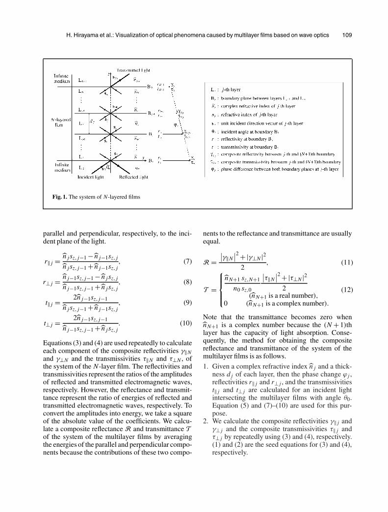
To visualize a light reflected on or passing throughmultilayer films consisting of dielectric, metallic,and/or semiconductive materials, it is necessaryto calculate a composite reflectance and transmit-tance of the multilayer film system based on waveopticsNow we consider the system of the multilayer filmsthat has N layers; the films are placed between twomedia (Fig. 1). The media extend infinitely in the op-posite directions of the interfaces of the films. Weassume the following preconditions for the multi-layer film system.
1. Each boundary plane between the layers is smoothand parallel to the xy plane in a local coordinatesystem, and each layer may have a different thick-ness. Based on this precondition, light reflects in
108 H. Hirayama et al.: Visualization of optical phenomena caused by multilayer films based on wave optics
the direction of mirror reflection, and transmitsin the direction obeying Snell’s law at the bound-aries between layers.
2. The media of each layer are homogeneous andisotropic. If the index of refraction changes con-tinuously inside a layer, the layer is further di-vided until it can be considered homogeneous.
3. Light comes in parallel to the zx plane from the0th layer, and intersects the boundary plane B1between the L0 and L1 layers. As a result of mul-tiple reflection and refraction of light inside thesystem of the multilayer films, the light is re-flected to the 0th layer and is transmitted to the(N + 1)th layer. A refractive index of the 0thlayer should be a real value, i.e., there is no ab-sorption in the 0th layer, since we assume the0th layer extends infinitely. If the layer has ab-sorption, light does not reach the boundary planeat all.
In the rendering process, incident light and films de-fined in world coordinates are transformed into localcoordinates defined in the preconditions, and com-posite reflectance and transmittance of the systemof the multilayer films are calculated by a recursivecomposition method, which is described in the nextsection.
2.2 Recursive composition method
We consider the system of multilayer films shownin Fig. 1. Specifying a thickness and a refractive in-dex for each layer, we can calculate reflectivity andtransmissivity of each boundary plane based on waveoptics [1]. Reflectivity and transmissivity are ratiosof amplitudes of incident electromagnetic waves ver-sus reflected and transmitted electromagnetic waves,respectively. Taking into consideration phase differ-ences between both boundaries of layers, we makea composite of the reflectivity and transmissivity inthe order of the boundary planes from BN+1 to B1.Finally, the composite reflectivity and transmissiv-ity are converted into reflectance and transmittance,which represent ratios of the energies of electromag-netic waves.Assuming that the thickness and complex refrac-tive index of jth layer are d j and n̂ j , respectively,the composite reflectivity and transmissivity be-tween the BN+1 and B j+1 boundaries are γN− j andτN− j , respectively. The composite reflectivity γ0 andthe transmissivity τ0 are those of the last boundary
planes BN+1. The seed equations at the BN+1 bound-ary plane are
γ0 = rN+1, (1)τ0 = tN+1, (2)
where rN+1 and tN+1 are the reflectivity and trans-missivity at a single boundary BN+1. After we com-pute the composite reflectivity γN− j and the trans-missivity τN− j , the composite reflectivity and trans-missivity of the next boundary plane under the condi-tion of multiple reflection and refraction can be cal-culated with the following recurrence equations [1,11] (see Appendix).
γN− j+1 = r j +γN− j e2iϕ j
1+r j γN− j e2iϕ j, (3)
τN− j+1 = t jτN− j eiϕ j
1+r j γN− j e2iϕ j, (4)
where i denotes an imaginary number, r j and t j arethe reflectivity and transmissivity at a single bound-ary B j , respectively. ϕ j is the phase difference be-tween boundary planes B j and B j+1, and is ex-pressed by the following equation.
ϕ j = 2π
λn̂ jd jsz, j, (5)
where λ is the wavelength of light in a vacuum, d jis the thickness of jth layer, sz, j is a z componentof the unit vector s j that indicates the direction oflight in jth layer, and n̂ j is the complex refractiveindex consisting of a refractive index n j and an ex-tinction coefficient κ j , (̂n j = n j + i κ j). The unit di-rection vector s j = (sx, j, sy, j, sz, j), is derived fromSnell’s law.
sx, j = n0 sin θ0
n̂ j, sy, j = 0, sz, j =
√1− s2
x, j . (6)
Note that the unit direction vector s j of each layer isderived from the refractive index n0 the incident an-gle θ0 of the 0th layer, and the complex refractive in-dex n̂ j of each layer, as we consider a system of mul-tilayer films with boundary planes that are parallel toeach other. The reflectivity r j and the transmissivityt j at boundary plane B j are derived by Fresnel for-mulae. They are represented by a component ‖ anda component ⊥ of the electromagnetic waves that are
H. Hirayama et al.: Visualization of optical phenomena caused by multilayer films based on wave optics 109
Fig. 1. The system of N-layered films
parallel and perpendicular, respectively, to the inci-dent plane of the light.
r‖ j = n̂ j sz, j−1 − n̂ j−1sz, j
n̂ j sz, j−1 + n̂ j−1sz, j, (7)
r⊥ j = n̂ j−1sz, j−1 − n̂ j sz, j
n̂ j−1sz, j−1 + n̂ j sz, j, (8)
t‖ j = 2̂n j−1sz, j−1
n̂ j sz, j−1 + n̂ j−1sz, j, (9)
t⊥ j = 2̂n j−1sz, j−1
n̂ j−1sz, j−1 + n̂ j sz, j. (10)
Equations (3) and (4) are used repeatedly to calculateeach component of the composite reflectivities γ‖Nand γ⊥N and the transmissivities τ‖N and τ⊥N , ofthe system of the N-layer film. The reflectivities andtransmissivities represent the ratios of the amplitudesof reflected and transmitted electromagnetic waves,respectively. However, the reflectance and transmit-tance represent the ratio of energies of reflected andtransmitted electromagnetic waves, respectively. Toconvert the amplitudes into energy, we take a squareof the absolute value of the coefficients. We calcu-late a composite reflectance R and transmittance Tof the system of the multilayer films by averagingthe energies of the parallel and perpendicular compo-nents because the contributions of these two compo-
nents to the reflectance and transmittance are usuallyequal.
R =∣∣γ‖N
∣∣2 +|γ⊥N |22
, (11)
T =
n̂N+1 sz,N+1
n0 sz,0
∣∣τ‖N∣∣2 +|τ⊥N |2
2(̂nN+1 is a real number),
0 (̂nN+1 is a complex number).
(12)
Note that the transmittance becomes zero whenn̂N+1 is a complex number because the (N + 1)thlayer has the capacity of light absorption. Conse-quently, the method for obtaining the compositereflectance and transmittance of the system of themultilayer films is as follows.
1. Given a complex refractive index n̂ j and a thick-ness d j of each layer, then the phase change ϕ j ,reflectivities r‖ j and r⊥ j , and the transmissivitiest‖ j and t⊥ j are calculated for an incident lightintersecting the multilayer films with angle θ0.Equation (5) and (7)–(10) are used for this pur-pose.
2. We calculate the composite reflectivities γ‖ j andγ⊥ j and the composite transmissivities τ‖ j andτ⊥ j by repeatedly using (3) and (4), respectively.(1) and (2) are the seed equations for (3) and (4),respectively.
110 H. Hirayama et al.: Visualization of optical phenomena caused by multilayer films based on wave optics
3. We calculate a composite reflectance R anda composite transmittance T of the system of themultilayer films with (11) and (12), respectively.
2.3 Discussion of multiple reflection andrefraction
In this section, we discuss how important the con-sideration of multiple reflections and refractions in-side films is for calculating composite reflectancesand transmittances. Figure 2 shows the simulationresults of reflectances and transmittances under theconditions of limited numbers of multiple reflectionsand refractions. We calculate these reflectances andtransmittances with (11), (12), (14), and (15), chang-ing the number of reflections and refractions m (seeFig. 11). In the simulation, the dielectric mediumwith a refractive index of 2.0 is coated with a 10 nmgold film.As shown in the simulation results (Fig. 2), the num-ber of multiple reflections and refractions of lightplays an important role in the accurate calculationof reflectances and transmittances. Even in the caseof the fifth reflection and refraction, an approxima-tion error remains. To make matters worse, when thenumber of reflections and refractions is small (e.g.,m = 0, 1), the transmittance exceeds 1.0. The largerthe reflectance of multilayer films, the more care-fully the number of multiple reflections and refrac-tions should be taken into account. With the pro-posed method, we can calculated the reflectancesand transmittances of a multilayer film system, tak-ing into account the infinite number of multiple re-flections and refractions at all the boundaries of thesystem.
3 Implementation of the multilayerfilm raytracer
We extend the raytracer proposed by Hirayama etal. [11] to visualize both dielectric multilayers andmultilayers with absorption of light such as thosewith metallic or semiconductive films. In this sec-tion, we discuss the implementation of the multilayerfilm raytracer.Figure 3 shows an algorithm of our raytracer. Theraytracer calculates a composite reflectance andtransmittance for each wavelength of light prior tothe raytracing process. In the raytracing process,
a
bFig. 2a,b. Simulation results of reflectances and transmit-tances: a reflectance of a film; b transmittance of a film.[L0, air, L1, 10 nm gold; L2, dielectric (n = 2.0)]
a spectral distribution of light is calculated for eachray. Finally, spectral distributions of light rays areconverted into RGB values to display a generatedimage on a monitor.
3.1 Calculation of composite reflectancesand transmittances
Reflection and transmission properties of multilayerfilms are determined by refractive indices and thick-nesses consisting of the system of the multilayerfilms. In the modeling process, refractive indicesand thicknesses of each film are specified as sur-face attributes of objects. In the rendering prepro-cess, composite reflectances and transmittances of
H. Hirayama et al.: Visualization of optical phenomena caused by multilayer films based on wave optics 111
the system of multilayer films are calculated by theproposed method, described in Sect. 2, for each sam-pled incident angle and wavelength of light. Thisinformation is then stored in tables. Note that thesetables are two dimensional, as the reflectance andtransmittance depend on both an incident angle anda wavelength of light. Furthermore, two tables arerequired when (1) each side of a multilayer filmfaces different kinds of media, and (2) light rayscome from both sides of the films, as the compos-ite reflectances and transmittances are different ac-cording to the interface with which a light ray firstintersects.If the size of all the tables exceeds the memory ca-pacity of a computer, these tables can be compressedwith an advanced compression algorithm, such asa wavelet composition.
3.2 Raytracing process
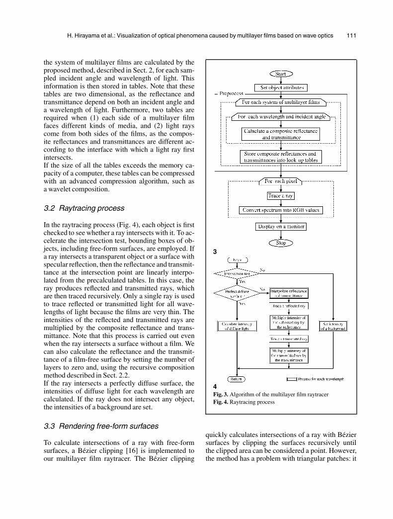
In the raytracing process (Fig. 4), each object is firstchecked to see whether a ray intersects with it. To ac-celerate the intersection test, bounding boxes of ob-jects, including free-form surfaces, are employed. Ifa ray intersects a transparent object or a surface withspecular reflection, then the reflectance and transmit-tance at the intersection point are linearly interpo-lated from the precalculated tables. In this case, theray produces reflected and transmitted rays, whichare then traced recursively. Only a single ray is usedto trace reflected or transmitted light for all wave-lengths of light because the films are very thin. Theintensities of the reflected and transmitted rays aremultiplied by the composite reflectance and trans-mittance. Note that this process is carried out evenwhen the ray intersects a surface without a film. Wecan also calculate the reflectance and the transmit-tance of a film-free surface by setting the number oflayers to zero and, using the recursive compositionmethod described in Sect. 2.2.If the ray intersects a perfectly diffuse surface, theintensities of diffuse light for each wavelength arecalculated. If the ray does not intersect any object,the intensities of a background are set.
3.3 Rendering free-form surfaces
To calculate intersections of a ray with free-formsurfaces, a Bézier clipping [16] is implemented toour multilayer film raytracer. The Bézier clipping
3
4Fig. 3. Algorithm of the multilayer film raytracerFig. 4. Raytracing process
quickly calculates intersections of a ray with Béziersurfaces by clipping the surfaces recursively untilthe clipped area can be considered a point. However,the method has a problem with triangular patches: it
112 H. Hirayama et al.: Visualization of optical phenomena caused by multilayer films based on wave optics
fails to calculate intersections near the degeneratedvertex of a triangular Bézier patch (for example, thetop of the handle of a Utah teapot). This is becausethe surface is clipped repeatedly in (u, v) param-eter space. The method does not converge, as theclipped area does not become smaller in (u, v) pa-rameter space, while it converges enough in (x, y, z)coordinate space. To solve the problem, every timea triangular Bézier patch is clipped, the clipped re-gion of a u or v direction with a degenerated ver-tex is converted into (x, y, z) coordinate space, andthe convergence is judged in (x, y, z) coordinatespace.
3.4 Color representation by spectraldistributions
Conventional raytracers calculate the intensities ofRGB colors corresponding to red, green, and bluemonochromatic light. However, it is necessary to cal-culate the spectrum of light to accurately render opti-cal phenomena. Particularly in reflection, refraction,interference, and absorption of light inside films,the optical characteristics greatly depend on a lightwavelength. For this reason, our multilayer film ray-tracer calculates a spectrum distribution of light.There are several methods for sampling a wavelengthof light. An adaptive sampling is a good method fora lighting model in an interference-free environmentbecause we only take into account spectrum of light.In the interference environment, however, many fac-tors should be considered in the sampling of the lightwavelength, including spectrum of light, incident an-gles of light rays, and the reflectivities and transmis-sivities of boundaries of each layer. In the raytracer,a constant sampling is employed, i.e., the wavelengthof visible light (380 nm to 780 nm) is sampled every5 nm.After calculating reflected and transmitted light frommultilayer films, the light spectra are converted intoRGB values to display on a color monitor with thespectral tristimulus values of the RGB colorimetricsystem [6].
R =∑λ
rλIλ, G =∑λ
gλIλ, B =∑λ
bλIλ,
(13)
where λ is a sampled wavelength, rλ, gλ, and bλ arethe spectral tristimulus values, and Iλ is a spectrumof light for each sampled wavelength.
4 Examples
Interference colors caused by a SiO2 layer on a sil-icon base and a scene containing windowpanescoated with multilayer films were rendered to showthe usefulness of the proposed method. The refrac-tive indices used in these examples were obtained byPalik [18].
4.1 Interference color of a SiO2 layer ona silicon base
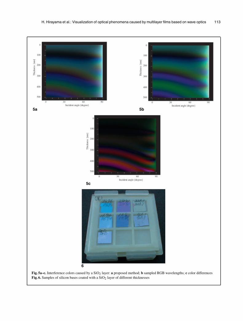
Figure 5a shows interference colors caused by a SiO2layer on a silicon base, and we calculated it withthe proposed method by sampling the wavelength ofvisible light every 5 nm. The horizontal and verticalaxes in Fig. 5 correspond to the incident angle of theviewing ray and the thickness of a SiO2 layer, respec-tively. The spectral distribution of a light source isset to the CIE standard illuminant D65 [7]. Figure 5bshows interference colors calculated by sampling theRGB colors corresponding to red (700 nm), green(545 nm), and blue (435 nm) monochromatic light.The color calculated by the proposed method is ac-curately simulated in the region where the incidentangle of light is nearly 90◦ (the reflectance of theSiO2 layer in this region is almost 1). Furthermore,when we compare the interference colors in thesefigures, we see that the thicker the SiO2 layer, themore the interference color differs. Figure 5c showsthe color differences between Fig. 5a and b, and theintensities of each pixel are multiplied by 3 to clearlyvisualize the differences. The maximal color differ-ences between Fig. 5a and b for the R, G, and B colorcomponents are 47, 33, and 43, respectively, in 256intensity levels.We also compared the interference colors in Fig. 5awith those of seven samples of silicon bases coatedwith SiO2 layers of different thicknesses (Fig. 6). Ifwe observe the samples from different viewing direc-tions, we see that the interference colors we visual-ized are almost the same as those of the samples.
4.2 Simulation of windowpanes coated withmultilayer films
Building windowpanes coated with multilayer filmsare rendered by our multilayer film raytracer. Re-flection and transmission properties of windowpanes
H. Hirayama et al.: Visualization of optical phenomena caused by multilayer films based on wave optics 113
5a 5b
5c
6
Fig. 5a–c. Interference colors caused by a SiO2 layer: a proposed method; b sampled RGB wavelengths; c color differencesFig. 6. Samples of silicon bases coated with a SiO2 layer of different thicknesses
114 H. Hirayama et al.: Visualization of optical phenomena caused by multilayer films based on wave optics
a b
c
d e
Fig. 7a–e. Windowpanes coated with various films: a aluminum film (5 nm); b aluminum film (10 nm); c aluminum film(20 nm); d multilayer metallic films; e dielectric and metallic films
coated with dielectric and metallic films are evalu-ated visually with the proposed method.Images of windowpanes rendered by the multi-layer film raytracer are shown in Fig. 7, and severalgraphs of reflectance distributions for incident an-gles and wavelength of light are shown in Fig. 8.Refractive indices of glass and a dielectric materialused in Fig. 7 are set to 1.6 and 2.0, respectively,for all visible wavelengths of light, and these ma-terials do not absorb any light. Films are coatedon the outside surfaces of the windowpanes, andthe film materials and their thicknesses are shown
in Table 1. Refractive indices of metallic materi-als, such as aluminum and gold, greatly dependon the wavelength of light, and were obtained byPalik [18]. The spectral distribution of the skycolor was calculated with an atmospheric scatteringmodel [17], and the spectral distribution of cloudswas considered as white light with an equal-energyspectrum.Figure 7a–c shows views of windowpanes coatedwith aluminum films of various thicknesses. Com-paring the panels of the figure, the thicker the alu-minum films, the more the sky is reflected in the
H. Hirayama et al.: Visualization of optical phenomena caused by multilayer films based on wave optics 115
a b
c
Fig. 8a–c. Graphs of reflectance distributions – windowpanes in: a Fig. 7b; b Fig. 7d; c Fig. 7e
windowpanes. In Fig. 7c, the inside of the building ishardly seen through the windowpanes, while the in-side can be seen in Fig. 7a. This is because the thickerthe film, the larger the reflectance of the window-panes coated with an aluminum film becomes. Theabsorption of light inside the aluminum films also in-creases, and the transmittance of the windowpanesbecomes smaller.Figure 7d shows windowpanes coated with mul-tilayer films consisting of gold and aluminum.The blue sky is not reflected much in the win-dowpanes, while clouds are reflected clearly. Thisis because the reflectance of light with a shortwavelength is lower than that with a long wave-length (Fig. 8b). Figure 7e shows windowpanes
coated with both dielectric and metallic films. Thecolor of clouds reflected in the windowpanes areyellow or purple, because of the interference in-side the dielectric films. The reflectance distribu-tion of the windowpanes in Fig. 7e is shown inFig. 8c.The size of the rendered images in Fig. 7 is 1000×600 pixels, and it took 5 min to render each im-age on an Alpha CPU (633 MHz) workstation, in-cluding the computation time for the preprocess ofrendering.These figures visualize the properties of reflectanceand transmittance of windowpanes coated with vari-ous kinds of films, and provide easy understanding ofthe optical properties of multilayer films.
116 H. Hirayama et al.: Visualization of optical phenomena caused by multilayer films based on wave optics
a b
c
Fig. 9a–c. Glasses coated with: a dielectric multilayer films; b 300 nm dielectric and 5 nm aluminum films; c 300 nmdielectric and 10 nm aluminum films
4.3 Glasses and teapots coated with films
To show the usefulness of our raytracer for designingvarious kinds of industrial products having free-formsurfaces, several images of glasses and teapots mod-eled with Bézier surfaces were rendered.In Fig. 9a, glasses are coated with six-layered filmsconsisting of two kinds of 100 nm dielectric filmswith refractive indices of 2.0 and 1.6 alternately,while, in Fig. 9b and c, glasses are coated withmultilayer films consisting of a dielectric with a re-fractive index of 2.0 and an aluminum film. Lensesof the glasses are modeled with 24 Bézier patches,and are made of dielectric media with refractive in-dices of 1.6. A point light source with the sepectraldistribution of the CIE standard illuminant D65 [7]is set above the glasses. With dielectric multilayerfilms, light is almost transmitted through the lenses
(Fig. 9a), while the checkered plate reflected into thelenses with a metallic film can be observed in Fig. 9b,and the lenses look bluish because of light absorp-tion due to an aluminum layer. The thicker the alu-minum film, the less the light is transmitted throughthe lenses, and light is almost reflected on the lensesas shown in Fig. 9c.Figure 10a shows a teapot made of silicon coatedwith a 500 nm SiO2 film. Figure 10b shows a glassteapot coated with a 20 nm gold film, while Fig. 10cshows a glass teapot coated with 10 nm aluminum,20 nm gold, and 500 nm dielectric films. A check-ered plate under the teapot is made of silver and cop-per, except in Fig. 10d. A point light source with thesepectral distribution of the CIE standard illuminantD65 [7] is set above the teapot.Color changes of interference inside a SiO2 film ap-pear on the surface of the teapot in Fig. 10a. In
H. Hirayama et al.: Visualization of optical phenomena caused by multilayer films based on wave optics 117
a b
c d
Fig. 10a–d. Silicon teapot coated with a SiO2 film; b glass teapot with gold film; c glass teapot with aluminum, gold anddielectric films; d silicon teapot with SiO2 film, copper cylinder with a gold film, and copper sphere with a silver film
Fig. 10b, absorption of light occurs inside a gold filmdue to the complex refraction index of gold, but somelight is transmitted by the teapot because the goldfilm is very thin. In Fig. 10c, both interference andabsorption of light are observed, and the surface ofthe teapot is reddish due to interference of light in-side the dielectric film.In Fig. 10d, a silicon teapot, a copper cylinder,and a copper sphere are coated with a 500 nmSiO2 film, a 50 nm silver film, and a 50 nm goldfilm, respectively. The checkered plate under theteapot is a diffuse surface. To visualize the ef-fects of the thickness of each film, two kinds ofanimations are generated, so that the thickness ofeach film changes from 1 nm to 50 nm for thesilver and gold films, and from 1 nm to 500 nmfor the SiO2 film (see http://www.eml.hiroshima-u.ac.jp/gallery/Animation/film/index.html).
5 Conclusions
In this paper, we have proposed a method for ren-dering objects coated with multilayer films consist-ing of dielectric, metallic and/or semiconductivematerials, taking into consideration complex refrac-tive indices. We implemented the proposed methodin a raytracer called the multilayer film raytracer,and rendered objects coated with different kindsof multilayer thin films to show the usefulness ofthe method. The proposed method makes it possi-ble to visualize accurate reflectance and transmit-tance properties of objects coated with multilayerfilms.The proposed method can handle only ideal smoothsurfaces coated with multilayer films. One of thefuture studies is developing a method for handlingrough surfaces coated with multilayer films.
118 H. Hirayama et al.: Visualization of optical phenomena caused by multilayer films based on wave optics
Acknowledgements. The authors thank Dr. Seiichi Miyazaki and Dr. At-sushi Kohno for their discussions and for providing the samples ofa SiO2 layer.
References
1. Born M, Wolf E (1997) Principles of optics. CambridgeUniversity Press, United Kingdom
2. Cook RL, Torrance KE (1982) A reflectance model forcomputer graphics. ACM Trans Graph 1:7–24
3. Dias ML (1991) Ray tracing interference color. IEEE Com-put Graph Appl 11:54–60
4. Dias ML (1994) Ray tracing interference color: visualizingnewton’s rings. IEEE Comput Graph Appl 14:17–20
5. Dorsey J, Hanrahan P (1996) Modeling and rendering ofmetallic paints. Proc. SIGGRAPH ’96 Annual ConferenceSeries on Computer Graphics, ACM SIGGRAPH, pp 387–396
6. Glassner AS (1995a) Principles of digital image synthesis1. Morgan Kaufmann, San Francisco, Calif, pp 44–51
7. Glassner AS (1995b) Principles of digital image synthesis2. Morgan Kaufmann, San Francisco, Calif, pp 1172–1175
8. Gondek JS, Meyer GW, Newman JG (1994) Wavelengthdependent reflectance functions. Proc. SIGGRAPH ’94 An-nual Conference Series on Computer Graphics, ACM SIG-GRAPH, pp 213–220
9. Hall RA, Greenberg DP (1983) A testbed for realistic imagesynthesis. IEEE Comput Graph Appl 3:10–20
10. Hanrahan P, Wolfgang K (1993) Reflection from layerd sur-faces due to subsurfaces scattering. Proc. SIGGRAPH ’93Annual Conference Series on Computer Graphics, ACMSIGGRAPH, pp 165–174
11. Hirayama H, Monden Y, Kaneda K, Yamashita H (1998)Scientific visualization of wave scattering phenomena oftransparent optical systems. (in Japanese) J Institute ImageElectronics Eng Japan 27:306–317
12. Icart I, Arques D (1999) An illumination model for a sys-tem of isotropic substrate-isotropic thin film with identicalrough boundaries. Proceedings of the 10th EurographicsWorkshop on Rendering, Granada, Spain, pp 261–272
13. Li J, Peng Q (1996) A new illumination model for scenescontaining thin film interference. Chinese J Electronics5:18–24
14. Moravec, HP (1981) 3D graphics and the wave theory.(SIGGRAPH ’81) Comput Graph 15:289–296
15. Nagata N, Dobashi T, Manabe Y, Usami T, Inokuchi S(1997) Modeling and visualization for a pearl-quality eval-uation simulator. IEEE Trans Vis Comput Graph 3:307–315
16. Nishita T, Sederberg TW, Kakimoto M (1990) Ray tracingtrimmed rational surface patches. (SIGGRAPH ’90) Com-put Graph 24(4):337–345
17. Nishita T, Sirai T, Tadamura K, Nakamae E (1993) Dis-play of the earth taking into account atmospheric scattering.(SIGGRAPH ’93) Annual Conference Series on ComputerGraphics, ACM SIGGRAPH, pp 175–182
18. Palik ED (1985) Handbook of optical constants of solids.Academic Press, Orlando
19. Smits BE, Meyer GW (1990) Newton’s colors: Simulatinginterference phenomena in realistic image synthesis. Pro-
ceedings of Eurographics Workshop on Photosimulation,Realism and Physics. Comput Graph pp 185–194
20. Suzuki N, Yokoi S, Toriwaki J (1993) Study on color com-putation in computer graphics and it’s application to render-ing color caused by light interference. (in Japanese) IEICETechnical Report of Japan 88:41–48
21. Thomas SW (1986) Dispersive refraction in ray tracing. Vi-sual Comput 2:3–8
22. Yasuda T, Yokoi S, Toriwaki J, Tsuruoka S, Miyake Y(1984) An improved ray tracing algorithm for renderingtransparent objects. (in Japanese) Trans Inform Process SocJapan 25:953–959
Recurrence equations of compositereflectivity and transmissivity
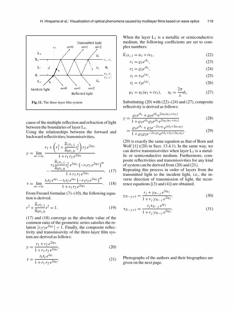
Let us consider a three-layer film system consistingof dielectric or metallic films (Fig. 11). The general-ized recurrence equations of the film system can bederived from complex refractive indicies. In the caseof a dielectric film, the recurrence equations are ob-tained by simply replacing the complex number witha real number.In Fig. 11, light comes from layer L0, and is transmit-ted to layer L2 with multiple reflection and refractioninside layer L1. Assuming that the forward reflectiv-ity and transmissivity at boundary B1 are r1 and t1,respectively, and the backward reflectivity and trans-missivity, i.e., those which light travels from layerL1 to layer L0 are r ′
1 and t′1, respectively, then thecomposite reflectivity γ and transmissivity τ of thethree-layer system are expressed as follows:
γ = r1 +∞∑
m=1
r2t1t′1e2iϕ1(
r ′1r2e2iϕ1
)m−1, (14)
τ =∞∑
m=0
t1t2eiϕ1(
r ′1r2e2iϕ1
)m, (15)
where ϕ1 is the phase difference between the bound-aries of layer L1,
ϕ1 = 2π
λn̂1d1sz,1, (16)
where λ is the wavelength of light in a vacuum, andn̂1 is the complex refractive index, d1 is the thick-ness, and sz,1 is a z component of the unit vector s1that indicates the direction of light in layer L1. Notethat (14) and (15) are infinite geometric series be-
H. Hirayama et al.: Visualization of optical phenomena caused by multilayer films based on wave optics 119
Fig. 11. The three-layer film system
cause of the multiple reflection and refraction of lightbetween the boundaries of layer L1.Using the relationships between the forward andbackward reflectivities/transmissivities,
γ = limm→∞
r1 +(
r21 + n̂1sz,1
n̂0sz,0t21
)r2 e2iϕ1
1+r1 r2 e2iϕ1
−r2
n̂1sz,1
n̂0sz,0t21 e2iϕ1
(−r1r2 e2iϕ1)m
1+r1 r2 e2iϕ1, (17)
τ = limm→∞
t1t2 eiϕ1 − t1t2 eiϕ1(−r1r2 e2iϕ1
)m
1+r1 r2 e2iϕ1. (18)
From Fresnel formulae (7)–(10), the following equa-tion is derived.
r2 + n̂1sz,1
n̂0sz,0t2 = 1. (19)
(17) and (18) converge as the absolute value of thecommon ratio of the geometric series satisfies the re-lation
∣∣r1r2e2iϕ1∣∣ < 1. Finally, the composite reflec-
tivity and transmissivity of the three-layer film sys-tem are derived as follows:
γ = r1 +r2 e2iϕ1
1+r1 r2 e2iϕ1, (20)
τ = t1t2 eiϕ1
1+r1 r2 e2iϕ1. (21)
When the layer L1 is a metallic or semiconductivemedium, the following coefficients are set to com-plex numbers:
n̂1sz,1 = u1 + iv1, (22)
r1 = �1eiδ1, (23)
r2 = �2eiδ2, (24)
t1 = τ1eiχ1, (25)
t2 = τ2eiχ2, (26)
ϕ1 = η1(u1 + iv1), η1 = 2π
λd1. (27)
Substituting (20) with (22)–(24) and (27), compositereflectivity is derived as follows:
γ = �1eiδ1 +�2eiδ2e2iη1(u1+iv1)
1+�1eiδ1�2eiδ1e2iη1(u1+iv1)(28)
= �1eiδ1 +�2e−2v1η1ei(δ2+2u1η1)
1+�1�2e−2v1η1ei(δ1+δ2+2u1η1). (29)
(29) is exactly the same equation as that of Born andWolf [1] ((20) in Sect. 13.4.1). In the same way, wecan derive transmissivities when layer L1 is a metal-lic or semiconductive medium. Furthermore, com-posite reflectivities and transmissivities for any kindof system can be derived from (20) and (21).Repeating this process in order of layers from thetransmitted light to the incident light, i.e., the in-verse direction of transmission of light, the recur-rence equations [(3) and (4)] are obtained.
γN− j+1 = r j +γN− j e2iϕ j
1+r j γN− j e2iϕ j, (30)
τN− j+1 = t jτN− j eiϕ j
1+r j γN− j e2iϕ j. (31)
Photographs of the authors and their biographies aregiven on the next page.
120 H. Hirayama et al.: Visualization of optical phenomena caused by multilayer films based on wave optics
HIDEKI HIRAYAMA is cur-rently a PhD candidate at theGraduate School of Engineer-ing, Hiroshima University, Hi-roshima Japan. He received hisBSc and MSc in Computer Sci-ence from Shimane University,Japan, in 1996 and 1998, re-spectively. His research interestsinclude scientific visualizationof physical phenomena and an-imation of human motions. Heis a member of the InformationProcessing Society of Japan and
the Institute of Electronics, Information and CommunicationEngineers.
KAZUFUMI KANEDA isan Associate Professor in theFaculty of Engineering at Hi-roshima University. He workedat Chugoku Electric Power,Japan, from 1984 to 1986. Hejoined Hiroshima University in1986. He was a Visiting Re-searcher in Engineering Com-puter Graphics Laboratory atBrigham Young University in1991. He received his BE, ME,and DE in 1982, 1984, and 1991,respectively, from Hiroshima
University. His research interests include computer graphics,scientific visualization, and image processing. He is a memberof the ACM, the IPSJ, the IEICE, and the IEEJ.
HIDEO YAMASHITA hasbeen a Professor at the De-partment of Electrical Engineer-ing, Hiroshima University, Hi-roshima, Japan since 1992. Hereceived his BE and ME inElectrical Engineering from Hi-roshima University, in 1964 and1968, respectively, and a PhDin Electrical Engineering fromWaseda University, Tokyo, Japan,in 1977. His interests includeelectric and magnetic fields,analysis of electric machinery by
finite element analysis, and visualization of 3D magnetic fieldsby computer graphics. He is a member of the Institute of Elec-trical Engineering of Japan and the IEEE.
YOSHIKI YAMAJI is cur-rently a graduate student at theGraduate School of Engineering,Hiroshima University, Japan.He received his BE in Electri-cal Engineering from HiroshimaUniversity, Hiroshima, Japan,in 1998. His research interestsinclude modeling and visualiza-tion. He is a member of Informa-tion Processing Society of Japan.
YOSHIMI MONDEN wasborn in Hiroshima, Japan, in1943 and is now with the Fac-ulty of Science and Engineering,Shimane University. His currentresearch interests are in alge-braic algorithms of system the-ory, discrete modeling of physi-cal systems, and scientific visu-alization of physical phenomena.Dr. Monden is a member ofthe Institute of Electronics, In-formation and CommunicationEngineering of Japan, the Infor-
mation Processing Society of Japan, the Institute of ImageElectronics Engineers of Japan, the IEEE, and the ACM.