VITA 62 DC-DC Converter Rev 1.5 Page 1 of 29 08/2021 VITA 62 DC-DC Converter VITA 62 Power Supply VIT270wxx600yzzz Note: Product images may not highlight current product markings. Features & Benefits • OpenVPX™ – VITA 62 • 180 – 420V input voltage range • 600W output power • 3U OpenVPX power supply • Conduction cooled • 6 outputs • I 2 C™ monitoring and control • Remote voltage sense: VS1, VS2, VS3 • Parallel operation capable with proprietary wireless current sharing • Overcurrent, overvoltage and overtemperature protections • IPC 610 class 3 • No aluminum electrolytic capacitors • Enable, inhibit, system reset and power fail controls • Military standard compliance: [a] MIL-STD-704F MIL-STD-461F MIL-STD-810G Typical Applications • VPX power modules • Avionics • Shipborne electronics Product Description The Vicor VITA 62 power supply is a COTs power supply that is designed for 3U OpenVPX systems. The module utilizes Vicor proprietary technology to enable high efficiency and power density for this highly rugged, conduction-cooled model. Up to four power supplies can be paralleled to increase output power capability of VS1, VS2, VS3 outputs with proprietary wireless current sharing. Conventional current-share pins are eliminated. Current share accuracy is ±1A. [a] See detailed specifications
Transcript
VITA 62 DC-DC Converter Rev 1.5Page 1 of 29 08/2021
VITA 62 DC-DC Converter
VITA 62 Power SupplyVIT270wxx600yzzz
Note: Product images may not highlight current product markings.
Features & Benefits
• OpenVPX™ – VITA 62
• 180 – 420V input voltage range
• 600W output power
• 3U OpenVPX power supply
• Conduction cooled
• 6 outputs
• I2C™ monitoring and control
• Remote voltage sense: VS1, VS2, VS3
• Parallel operation capable with proprietary wireless current sharing
• Overcurrent, overvoltage and overtemperature protections
• IPC 610 class 3
• No aluminum electrolytic capacitors
• Enable, inhibit, system reset and power fail controls
• Military standard compliance: [a]
� MIL-STD-704F� MIL-STD-461F� MIL-STD-810G
Typical Applications
• VPX power modules
• Avionics
• Shipborne electronics
Product Description
The Vicor VITA 62 power supply is a COTs power supply that is designed for 3U OpenVPX systems. The module utilizes Vicor proprietary technology to enable high efficiency and power density for this highly rugged, conduction-cooled model.
Up to four power supplies can be paralleled to increase output power capability of VS1, VS2, VS3 outputs with proprietary wireless current sharing. Conventional current-share pins are eliminated. Current share accuracy is ±1A.
[a] See detailed specifications
VITA 62 DC-DC Converter Rev 1.5Page 2 of 29 08/2021
VIT270wxx600yzzz
3U P0 Connector
P1 P2 LP1
1 2 3 4 5 6 7 8
P3 P4 P5 LP2 P6
ROWSSIGNAL
POWER POWER
DCBA
Connector Pin Configuration
Note: See mechanical drawing on page 28 for connector information.
VITA 62 DC-DC Converter Rev 1.5Page 3 of 29 08/2021
VIT270wxx600yzzz
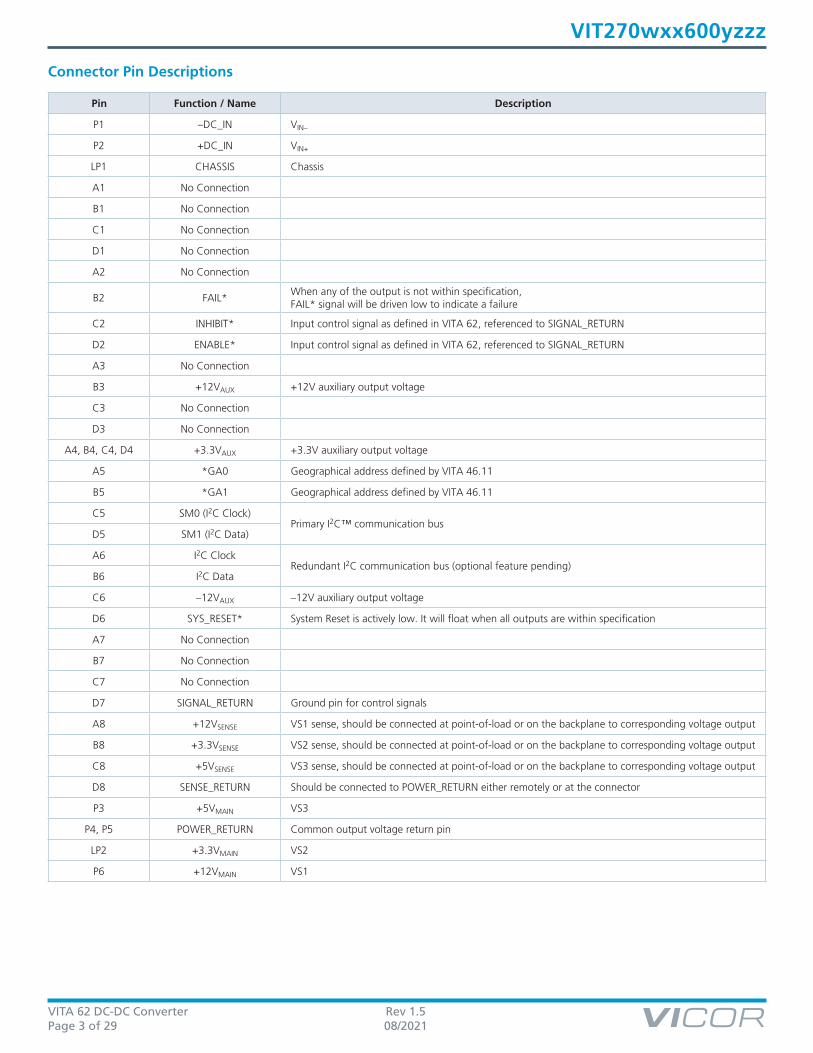
Connector Pin Descriptions
Pin Function / Name Description
P1 –DC_IN VIN–
P2 +DC_IN VIN+
LP1 CHASSIS Chassis
A1 No Connection
B1 No Connection
C1 No Connection
D1 No Connection
A2 No Connection
B2 FAIL*When any of the output is not within specification, FAIL* signal will be driven low to indicate a failure
C2 INHIBIT* Input control signal as defined in VITA 62, referenced to SIGNAL_RETURN
D2 ENABLE* Input control signal as defined in VITA 62, referenced to SIGNAL_RETURN
A3 No Connection
B3 +12VAUX +12V auxiliary output voltage
C3 No Connection
D3 No Connection
A4, B4, C4, D4 +3.3VAUX +3.3V auxiliary output voltage
A5 *GA0 Geographical address defined by VITA 46.11
B5 *GA1 Geographical address defined by VITA 46.11
C5 SM0 (I2C Clock)Primary I2C™ communication bus
D5 SM1 (I2C Data)
A6 I2C ClockRedundant I2C communication bus (optional feature pending)
B6 I2C Data
C6 –12VAUX –12V auxiliary output voltage
D6 SYS_RESET* System Reset is actively low. It will float when all outputs are within specification
A7 No Connection
B7 No Connection
C7 No Connection
D7 SIGNAL_RETURN Ground pin for control signals
A8 +12VSENSE VS1 sense, should be connected at point-of-load or on the backplane to corresponding voltage output
B8 +3.3VSENSE VS2 sense, should be connected at point-of-load or on the backplane to corresponding voltage output
C8 +5VSENSE VS3 sense, should be connected at point-of-load or on the backplane to corresponding voltage output
D8 SENSE_RETURN Should be connected to POWER_RETURN either remotely or at the connector
P3 +5VMAIN VS3
P4, P5 POWER_RETURN Common output voltage return pin
LP2 +3.3VMAIN VS2
P6 +12VMAIN VS1
VITA 62 DC-DC Converter Rev 1.5Page 4 of 29 08/2021
VIT270wxx600yzzz
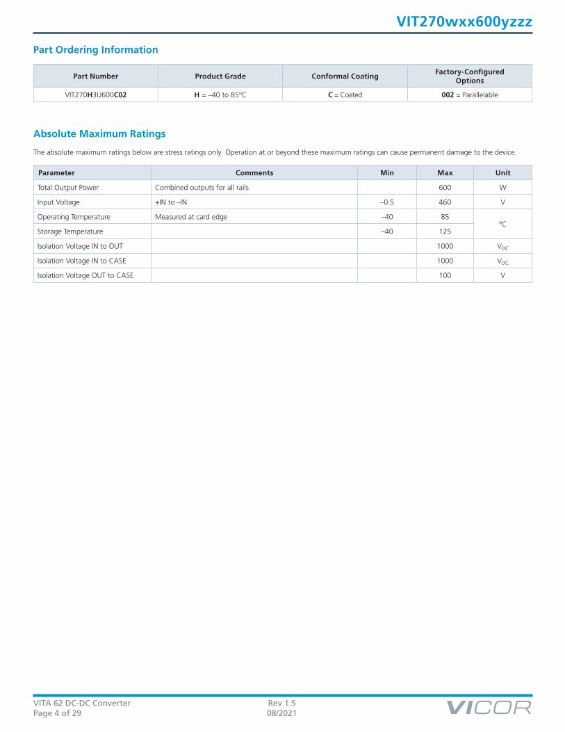
Part Ordering Information
Absolute Maximum Ratings
The absolute maximum ratings below are stress ratings only. Operation at or beyond these maximum ratings can cause permanent damage to the device.
Parameter Comments Min Max Unit
Total Output Power Combined outputs for all rails 600 W
Input Voltage +IN to –IN –0.5 460 V
Operating Temperature Measured at card edge –40 85ºC
Storage Temperature –40 125
Isolation Voltage IN to OUT 1000 VDC
Isolation Voltage IN to CASE 1000 VDC
Isolation Voltage OUT to CASE 100 V
Part Number Product Grade Conformal CoatingFactory-Configured
Options
VIT270H3U600C02 H = –40 to 85°C C = Coated 002 = Parallelable
VITA 62 DC-DC Converter Rev 1.5Page 5 of 29 08/2021
VIT270wxx600yzzz
Electrical Characteristics
All data at nominal line and nominal load unless otherwise specified.
Attribute Symbol Conditions / Notes Min Typ Max Unit
Overall System Characteristics
System Efficiency
Nominal line, 20% aggregate loads 83
%Nominal line, 50% aggregate loads 89
Nominal line, 100% aggregate loads 89
Power Input Characteristics
Operating Input Voltage Range Full load 180 270 420 V
Transient 450 V
Input Current (No Load)270V Input, enable asserted (input on), inhibit de-asserted (output on)
30 75 mA
Inrush Current Peak no load, high line 1.4 5 A
Main Outputs
+12V Output
Output Voltage Set Point Nominal line, nominal load 11.9 12 12.1 V
Line Regulation 50% load 0.12 0.2 %
Load Regulation Nominal line 0.5 %
Output Ripple / Noise (Peak-to-Peak) Nominal line over load range, 20MHz BW 50.4 120 mVP-P
Maximum Capacitive Load External 9000 µF
Output Current Range 0 40 A
Output Overvoltage Protection Two consecutive OVP events to trip 13.2 V
Output Overcurrent Protection Three consecutive OCP events to trip 48 A
+5V Output
Output Voltage Set Point Nominal line, nominal load 4.93 5.0 5.07 V
Line Regulation 50% load 0.15 %
Load Regulation Nominal line 0.5 1.1 %
Output Ripple / Noise (Peak-to-Peak) Nominal line over load range, 20MHz BW 20 50 mVP-P
Maximum Capacitive Load External 9000 µF
Output Current Range 0 30 A
Output Overvoltage Protection Two consecutive OVP events to trip 5.6 V
Output Overcurrent Protection Three consecutive OCP events to trip 40 A
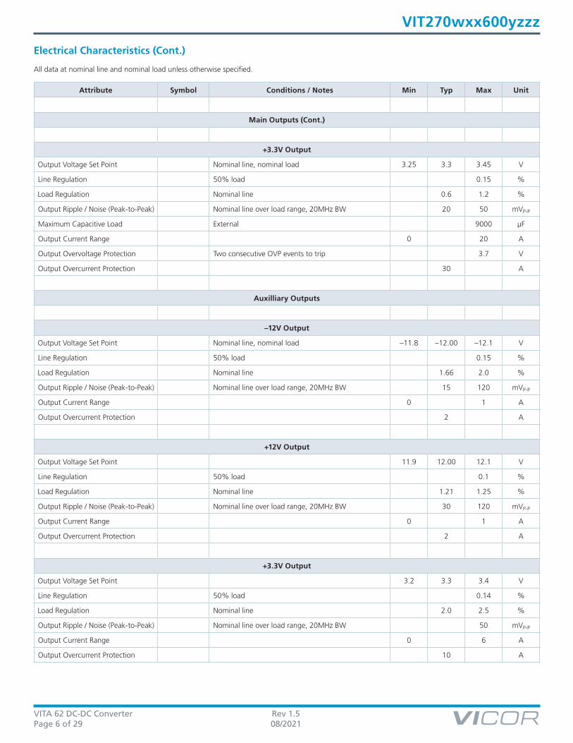
VITA 62 DC-DC Converter Rev 1.5Page 6 of 29 08/2021
VIT270wxx600yzzz
Attribute Symbol Conditions / Notes Min Typ Max Unit
Main Outputs (Cont.)
+3.3V Output
Output Voltage Set Point Nominal line, nominal load 3.25 3.3 3.45 V
Line Regulation 50% load 0.15 %
Load Regulation Nominal line 0.6 1.2 %
Output Ripple / Noise (Peak-to-Peak) Nominal line over load range, 20MHz BW 20 50 mVP-P
Maximum Capacitive Load External 9000 µF
Output Current Range 0 20 A
Output Overvoltage Protection Two consecutive OVP events to trip 3.7 V
Output Overcurrent Protection 30 A
Auxilliary Outputs
–12V Output
Output Voltage Set Point Nominal line, nominal load –11.8 –12.00 –12.1 V
Line Regulation 50% load 0.15 %
Load Regulation Nominal line 1.66 2.0 %
Output Ripple / Noise (Peak-to-Peak) Nominal line over load range, 20MHz BW 15 120 mVP-P
Output Current Range 0 1 A
Output Overcurrent Protection 2 A
+12V Output
Output Voltage Set Point 11.9 12.00 12.1 V
Line Regulation 50% load 0.1 %
Load Regulation Nominal line 1.21 1.25 %
Output Ripple / Noise (Peak-to-Peak) Nominal line over load range, 20MHz BW 30 120 mVP-P
Output Current Range 0 1 A
Output Overcurrent Protection 2 A
+3.3V Output
Output Voltage Set Point 3.2 3.3 3.4 V
Line Regulation 50% load 0.14 %
Load Regulation Nominal line 2.0 2.5 %
Output Ripple / Noise (Peak-to-Peak) Nominal line over load range, 20MHz BW 50 mVP-P
Output Current Range 0 6 A
Output Overcurrent Protection 10 A
Electrical Characteristics (Cont.)
All data at nominal line and nominal load unless otherwise specified.
VITA 62 DC-DC Converter Rev 1.5Page 7 of 29 08/2021
VIT270wxx600yzzz
Signal Characteristics
All of the following plots are at nominal line and 600W aggregate load unless otherwise noted.
ENABLE*: Enable*
• The ENABLE* pin or control register bit enables and disables the +3.3V AUX output of the power supply.• The ENABLE* pin has an internal pull-up to VCC and is referenced to the Signal Return pin of the power supply.
Signal Type State Attribute Symbol Conditions / Notes Min Typ Max Unit
Digital Input
Any
ENABLE* Enable Threshold VENABLE-EN 0.8 V
ENABLE* Disable Threshold
VENABLE-DIS 2.0 V
Internally Generated VCC VCC 3.21 3.30 3.39 V
ENABLE* Internal Pull-Up Resistance to VCC
RENABLE-INT 49 51 52 kΩ
ENABLE* Enable Debounce Delay
tD-EN-E 3 5 ms
ENABLE* Disable Debounce Delay
tD-EN-D 3 5 ms
INHIBIT*: Inhibit*
• The INHIBIT* pin enables and disables all outputs except +3.3VAUX if VENABLE-EN threshold has been met.• The INHIBIT* pin has an internal pull up to VCC and is referenced to the Signal Return pin of the power supply.
Signal Type State Attribute Symbol Conditions / Notes Min Typ Max Unit
Digital Input
Any
INHIBIT* Enable Threshold VINHIBIT-EN Status register bit 4 should be 0 (default) for digital input control line to have priority
2.0 V
INHIBIT* Disable Threshold VINHIBIT-DIS 0.8 V
Internally Generated VCC VCC 3.21 3.30 3.39 V
INHIBIT* Internal Pull-Up Resistance to VCC
RDISABLE-INT 49 51 52 kΩ
INHIBIT* Enable Debounce Delay after ENABLE*
tD-IN-E 3 5 ms
INHIBIT* Disable Debounce Delay
tD-IN-D 3 5 ms
Lockout Delay Between Consecutive INHIBIT* Enables
tD-IN-L 3 5 ms
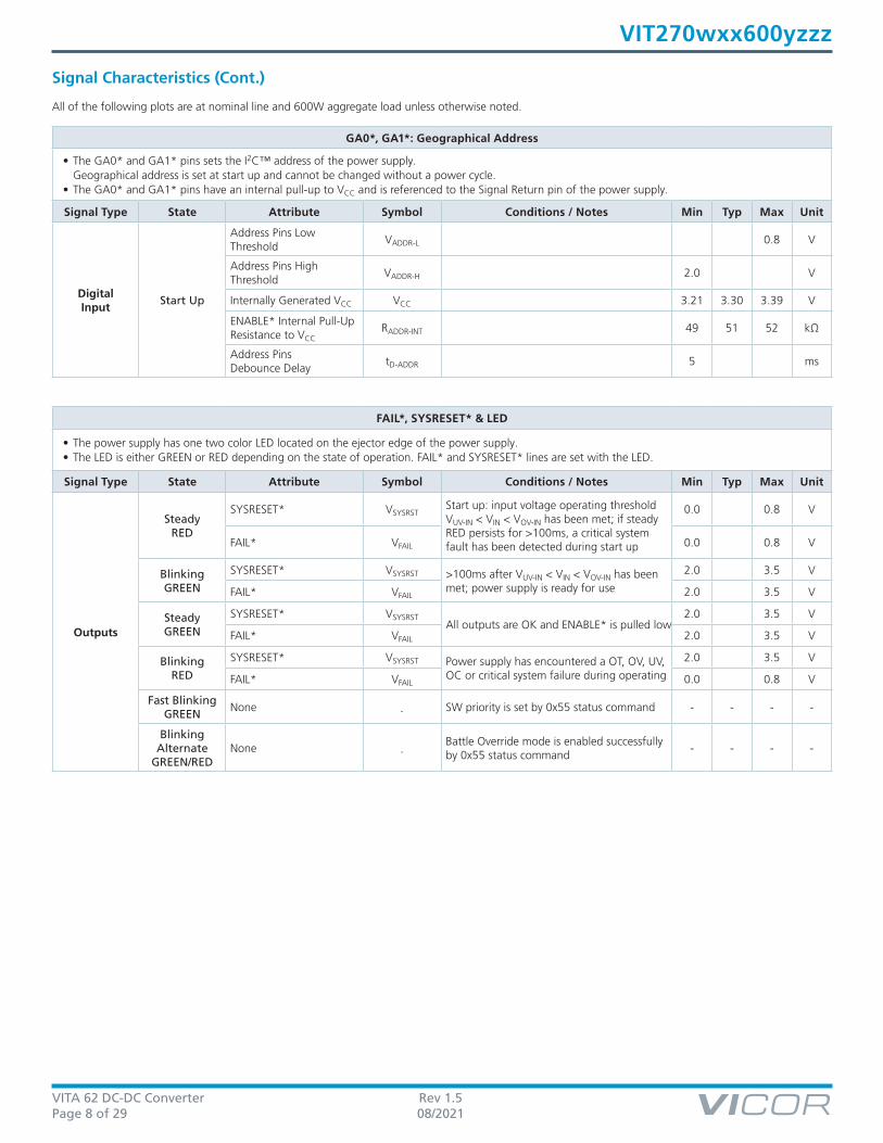
VITA 62 DC-DC Converter Rev 1.5Page 8 of 29 08/2021
VIT270wxx600yzzz
Signal Characteristics (Cont.)
All of the following plots are at nominal line and 600W aggregate load unless otherwise noted.
GA0*, GA1*: Geographical Address
• The GA0* and GA1* pins sets the I2C™ address of the power supply. Geographical address is set at start up and cannot be changed without a power cycle.
• The GA0* and GA1* pins have an internal pull-up to VCC and is referenced to the Signal Return pin of the power supply.
Signal Type State Attribute Symbol Conditions / Notes Min Typ Max Unit
Digital Input
Start Up
Address Pins Low Threshold
VADDR-L 0.8 V
Address Pins High Threshold
VADDR-H 2.0 V
Internally Generated VCC VCC 3.21 3.30 3.39 V
ENABLE* Internal Pull-Up Resistance to VCC
RADDR-INT 49 51 52 kΩ
Address Pins Debounce Delay
tD-ADDR 5 ms
FAIL*, SYSRESET* & LED
• The power supply has one two color LED located on the ejector edge of the power supply.• The LED is either GREEN or RED depending on the state of operation. FAIL* and SYSRESET* lines are set with the LED.
Signal Type State Attribute Symbol Conditions / Notes Min Typ Max Unit
Outputs
Steady RED
SYSRESET* VSYSRSTStart up: input voltage operating threshold VUV-IN < VIN < VOV-IN has been met; if steady RED persists for >100ms, a critical system fault has been detected during start up
0.0 0.8 V
FAIL* VFAIL 0.0 0.8 V
Blinking GREEN
SYSRESET* VSYSRST >100ms after VUV-IN < VIN < VOV-IN has been met; power supply is ready for use
2.0 3.5 V
FAIL* VFAIL 2.0 3.5 V
Steady GREEN
SYSRESET* VSYSRSTAll outputs are OK and ENABLE* is pulled low
2.0 3.5 V
FAIL* VFAIL 2.0 3.5 V
Blinking RED
SYSRESET* VSYSRST Power supply has encountered a OT, OV, UV, OC or critical system failure during operating
2.0 3.5 V
FAIL* VFAIL 0.0 0.8 V
Fast BlinkingGREEN
None - SW priority is set by 0x55 status command - - - -
Blinking Alternate
GREEN/REDNone -
Battle Override mode is enabled successfully by 0x55 status command
- - - -
VITA 62 DC-DC Converter Rev 1.5Page 9 of 29 08/2021
VIT270wxx600yzzz
Application Characteristics
Figure 1 — Turn-on and turn-off characteristics at nominal line and nominal load, to main outputs
Figure 2 — Turn-on and turn-off time from enable to outputs
VITA 62 DC-DC Converter Rev 1.5Page 10 of 29 08/2021
Telcordia Issue 2 - Method I Case III; 25°C Ground Benign, Controlled
709,585 Hrs
General Characteristics
VITA 62 DC-DC Converter Rev 1.5Page 14 of 29 08/2021
VIT270wxx600yzzz
GA0* GA1*
SYSRESET*
50kΩ
From IPMC
FAIL*
50kΩ
From IPMC
ENABLE* INHIBIT*
Signal Return
SW SW SW SW
5kΩ
VCC
50kΩ
RPU
VCC
RPU
I2C Clock
I2C Data
Buffers
IPMC
Signal Return
To IPMC
5kΩ
VCC
50kΩ
To IPMC
5kΩ
VCC
50kΩ
To IPMC
5kΩ
VCC VCC VCC
50kΩ
To IPMC
Typical External Circuits for Signal Pins (ENABLE*, INHIBIT*, GA0*, GA1*, SYSRESET*, FAIL* and I2C Channels)
Signal Pin Functions
ENABLE* & INHIBIT*
Enable and Inhibit pins express active low logic. Table 1 has the truth table for the output state of the power supply. It is necessary to avoid the indeterminate output state where 0.8 – 2.0V is applied to the ENABLE* or INHIBIT* pins.
A digital debounce filter is present on the signals of both pins to prevent false transitions. The ENABLE* and INHIBIT* also have a minimum delay between successive output enable transitions to prevent repeated starts into high capacitance loads. See detailed specifications for delays time limits.
Geographical Address: GA0* & GA1*
Geographical address pins also exhibit active low logic. Table 2 has the truth table for the output state of the power supply. It is necessary to avoid the indeterminate state where 0.8 – 2.0V is applied to either address pins. A digital debounce filter is present on the signals of both pins to incorrect address assignment.
The geographical address is static and set on power up. The power supply’s address cannot not change until power has been cycled and the states of the address pins have been modified before power up.
I2C Ports:
Both primary and redundant I2C™ ports have the same address set by the Geographical Address pins and identical functionality. There is a bidirectional buffer on both clock and data lines with internal pull ups on the IPMC and external pulls on the back plane to +3.3V are required.
FAIL*
This signal line is open drain and tracks SYSRESET* when the unit is powering up or pulled down to SIGNAL_RETURN when any of the outputs are out of specification. A pull up resistor is expected on the backplane per section 4.6.3.7 of VITA 62.
SYSRESET*
This signal line is open drain and is pulled down to SIGNAL_RETURN when the unit is powering up. The line is released when the power supply is ready for control. Appropriate pull-up/pull-down resistors are expected on the back plane per VITA 46 section 7.3.9.
SIGNAL RETURN
SIGNAL RETURN is used as the reference for signals pin connections and is to be tied to POWER_RETURN on the backplane per section 4.6.3.10-1 of VITA 62.
Table 1 — ENABLE & INHIBIT logic
Table 2 — Geographical address assignment
ENABLE* Pin INHIBIT* Pin Output State and Notes
< 0.8V, Logic 0 > 2.0V or NO, Logic 1 All outputs available
0.8V > VENABLE* < 2.0V 0.8V > VINHIBIT* < 2.0VIndeterminate state and must be avoided
GA1* GA0* Power Supply Address
> 2.0V or NO, Logic 1 > 2.0V or NO, Logic 1 20h
> 2.0V or NO, Logic 1 < 0.8V, Logic 0 21h
< 0.8V, Logic 0 > 2.0V or NO, Logic 1 22h
< 0.8V, Logic 0 < 0.8V, Logic 0 23h
0.8V > VGA1* < 2.0V 0.8V > VGA0* < 2.0VIndeterminate state and must be avoided
VITA 62 DC-DC Converter Rev 1.5Page 15 of 29 08/2021
VIT270wxx600yzzz
Card Edge Temperature Sensors
The PCBA card edge temperature sensor internal to the power supply is mounted on the edge of the PCBA card edge. Consequently, the temperature sensor measures a temperature that is generally higher than the heat-sink-to-rail mounting interface and lower than the hot spot of the internal converters in the power supply.
Response from the power supply to I2C™ command 0x21 provides the temperature measured by the internal sensor that reads the higher temperature. This temperature can exceed 85°C. I2C command 0x92 will respond with both PCB mounted temperature sensors.
Fault Operation
See Table 5 for nonrecoverable fault thresholds which trigger a fault and shut down/restart of the outputs of the supply.
Input Voltage Protection (IOVP)
If the input voltage to the power supply drops below VUV-IN or exceeds VOV-IN for at least 1ms, the power supply will shut down all outputs and digital communication lines until input voltage is within operating range VIN. Triggering IOVP has the same effect as power cycling the power supply. Supply currents and voltages are sampled every 200µs.
Output Voltage Protection (OOVP)
The power supply measures voltage from the remote-sense lines as well as the voltages on the VITA connector which do not include remote sense drop.
The FAIL* line will be asserted (pulled low) when output voltage at the connector of the power supply is greater than the nonrecoverable limit of any output. OVP will also shut down the outputs until the output voltage of the converter is within specification. The power supply will automatically restart the outputs every 1s until the fault clears.
Overcurrent Protection (OCP)*
During an overcurrent fault on any output, all outputs will shut off and the FAIL* line will be asserted. The power supply will automatically try to restart outputs every 1s if the fault has cleared.
Overtemperature Protection (OTP)
The power supply will go into overtemperature protection and shut down all outputs when either internal temperature sensor measures 95°C. The power converter will recover for normal operation when the internal temperature has dropped by 20°C.
At 85°C the Bit-5 of the Status Register (0x55) will clear if the system manager sets Bit-5 to 1 which will indicate the power supply is within 10°C from shutting down.
VITA 62 DC-DC Converter Rev 1.5Page 16 of 29 08/2021
VIT270wxx600yzzz
Parallel Operation
For proper load regulation and paralleling of like power supplies, a single kelvin connection between each sense pin and load is required. Under normal parallel power supply operation, each supply’s PoL regulated output will be at different voltage with respect to its own backplane connector to compensate for transmission voltage drop. Figure 32a depicts an instance of a backplane with three power supplies where the point-of-load (PoL) sense pins on each power supply are connected.
It is not recommended to connect the PoL sense pins in a manner depicted in Figure 32b where each supply’s PoL sense pins are connected to each other and also to each power supply’s own PoL voltage output. In this case the system may appear to function normally temporarily but load regulation and sharing are not guaranteed due to the lack of a kelvin connection between the supplies and a single load point.
All six outputs can be connected in parallel with the same output from other power supplies with the same part number. Only VS1, VS2 and VS3 support load sharing. The combined current output of paralleled AUX outputs is limited to the ampacity of respective individual AUX outputs of a single power supply.
Figure 9 — Sense pin connection arrangement connects all supplies to the backplane of the array
Required Sense pin connections on the backplane
of a three-unit parallel array
(a)
Not Recommended Connecting sense pins to each other and to each supply's own PoL voltage output
(b)
x
V
^Y
oooo
oooo
oooo
o
x
x
^Y
V
x
^Y
V
^Y
V
oo
o
Payload N
Payload 2
A8B8C8
A7B7C7
A7B7C7
A7B7C7
D8
VS1 Sense
VS3 SenseVS2 Sense
GND Sense
A8B8C8D8
A8B8C8D8
Payload 1
Supply 1
Supply 2
Supply 3
P6
LP2
P3P4, P5
P6
LP2
P3P4, P5
P6
LP2
P3P4, P5
oooo
oooo
oooo
x
x
^Y
V
x
^Y
V
^Y
V
Payload N
Payload 2
A8B8C8
A7B7C7
A7B7C7
A7B7C7
D8
A8B8C8D8
A8B8C8D8
Payload 1
Supply 1
Supply 2
Supply 3
P6
LP2
P3P4, P5
P6
LP2
P3P4, P5
P6
LP2
P3P4, P5
OutputMax Current vs. Paralleled Supplies
Unit1 2 3 4
VS1 (+12V) 40 72 108 144 A
VS2 (+3.3V) 20 36 54 72 A
VS3 (+5V) 30 54 81 108 A
VAUX1 (–12V) 1 1 1 1 A
VAUX2 (+3.3V) 6 6 6 6 A
VAUX3 (+12V) 1 1 1 1 A
Table 3 — Maximum current rating by output for parallel arrays
VITA 62 DC-DC Converter Rev 1.5Page 17 of 29 08/2021
VIT270wxx600yzzz
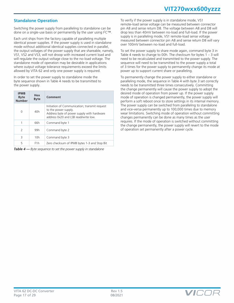
Standalone Operation
Switching the power supply from paralleling to standalone can be done on a single-use basis or permanently by the user using I2C™.
Each unit ships from the factory capable of paralleling multiple identical power supplies. If the power supply is used in standalone mode without additional identical supplies connected in parallel, the output voltages of the power supply that are shareable, namely, VS1, VS2 and VS3, will not droop with increased current load and will regulate the output voltage close to the no-load voltage. The standalone mode of operation may be desirable in applications where output voltage tolerance requirements exceed the limits allowed by VITA 62 and only one power supply is required.
In order to set the power supply to standalone mode the byte sequence shown in Table 4 needs to be transmitted to the power supply.
To verify if the power supply is in standalone mode, VS1 remote-load sense voltage can be measured between connector pin A8 and sense return D8. The voltage between A8 and D8 will drop less than 40mV between no-load and full-load. If the power supply is in paralleling mode, VS1 remote-load sense voltage measured between connector pin A8 and sense return D8 will vary over 100mV between no-load and full-load.
To set the power supply to share mode again, command byte 3 in Table 4 needs to change to 00h. The checksum for bytes 1 – 3 will need to be recalculated and transmitted to the power supply. The sequence will need to be transmitted to the power supply a total of 3 times for the power supply to permanently change its mode at power up to support current share or paralleling.
To permanently change the power supply to either standalone or paralleling mode, the sequence in Table 4 with byte 3 set correctly needs to be transmitted three times consecutively. Committing the change permanently will cause the power supply to adopt the desired mode of operation from power up. If the power supply mode of operation is changed permanently, the power supply will perform a soft reboot once to store settings in its internal memory. The power supply can be switched from paralleling to standalone and vice-versa permanently up to 100,000 times due to memory wear limitations. Switching mode of operation without committing changes permanently can be done as many times as the user requires. If the mode of operation is switched without committing the change permanently, the power supply will revert to the mode of operation set permanently after a power cycle.
IPMB Byte
Number
Hex Byte
Comment
0 40h
Initiation of Communication; transmit request to the power supply. Address byte of power supply with hardware address 0x20 and LSB read/write low.
1 66h Command byte 1
2 99h Command byte 2
3 10h Command byte 3
5 F1h Zero checksum of IPMB bytes 1-3 and Stop Bit
Table 4 — Byte sequence to set the power supply in standalone
VITA 62 DC-DC Converter Rev 1.5Page 18 of 29 08/2021
VIT270wxx600yzzz
Conducted Emissions Testing
Professional Testing, EMI, IncMIL-STD-461, CE102, Conducted Emissions, Power LeadsLine 1 Measured Emissions
Frequency10K 100K 1M 10M
10
20
30
40
50
60
70
80
90
100
110
Am
plit
ud
e (d
BµV
)
Client: Freedom Power Systems
Project Number: 20125-10
EUT Name: 01-739-0003 Power Supply
Current Time -12:19:02 PM, Monday, July 09, 2018
Operator: Michael Anthony
Line Under Test: Power 270VDC input EUT Mode: FULL Load Note:
Limit Level
Ambient Scan
Measured Value
Professional Testing, EMI, IncMIL-STD-461, CE102, Conducted Emissions, Power LeadsLine 2 Measured Emissions
Frequency10K 100K 1M 10M
10
20
30
40
50
60
70
80
90
100
110
Am
plit
ud
e (d
BµV
)
Client: Freedom Power Systems
Project Number: 20125-10
EUT Name: 01-739-0003 Power Supply
Current Time -12:16:57 PM, Monday, July 09, 2018
Operator: Michael Anthony
Line Under Test: Return EUT Mode: FULL Load Note:
Limit Level
Ambient Scan
Measured Value
Figure 10 — Conducted emissions of 270VDC input at full load
Figure 11 — Conducted emissions of power return at full load
VITA 62 DC-DC Converter Rev 1.5Page 19 of 29 08/2021
VIT270wxx600yzzz
Conducted Emissions Testing (Cont.)
Professional Testing, EMI, IncMIL-STD-461, CE102, Conducted Emissions, Power LeadsLine 1 Measured Emissions
Frequency10K 100K 1M 10M
10
20
30
40
50
60
70
80
90
100
110
Am
plit
ud
e (d
BµV
)
Client: Freedom Power Systems
Project Number: 20125-10
EUT Name: 01-739-0003 Power Supply
Current Time -12:26:02 PM, Monday, July 09, 2018
Operator: Michael Anthony
Line Under Test: Power 270VDC input EUT Mode: NO Load Note:
Limit Level
Ambient Scan
Measured Value
Professional Testing, EMI, IncMIL-STD-461, CE102, Conducted Emissions, Power LeadsLine 2 Measured Emissions
Frequency10K 100K 1M 10M
10
20
30
40
50
60
70
80
90
100
110
Am
plit
ud
e (d
BµV
)
Client: Freedom Power Systems
Project Number: 20125-10
EUT Name: 01-739-0003 Power Supply
Current Time -12:28:31 PM, Monday, July 09, 2018
Operator: Michael Anthony
Line Under Test: Return EUT Mode: NO Load Note:
Limit Level
Ambient Scan
Measured Value
Figure 12 — Conducted emissions of 270VDC input at no load
Figure 13 — Conducted emissions of power return at no load
VITA 62 DC-DC Converter Rev 1.5Page 20 of 29 08/2021
Pass40g, 11ms, terminal saw tooth shock pulses in all three axes
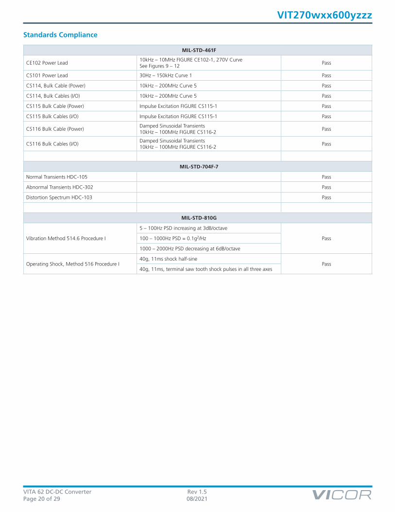
Standards Compliance
VITA 62 DC-DC Converter Rev 1.5Page 21 of 29 08/2021
VIT270wxx600yzzz
I2C™ Sensor Commands
Commands are sent by SMBus-compatible packets over the I2C physical interface. The I2C bus will communicate at 100kHz. Pull-up resistors to +3.3V are expected on the system backplane.
Two pins, labeled *GA1 and *GA0 are provided at each power supply slot, where *GA1 and *GA0 are defined to be active (SET) when low. The power supply will respond to I2C address 010 00[GA1][GA0].
The power supply supports commands to read sensor data from the power supply without utilizing VITA 46.11 or IPMI. The commands are similar to register reads in from I2C memory and function in a parent/child configuration. Unlike VITA 46.11 which is a multi-parent protocol, commands defined in this section are parent-write and parent-read.
Table 5 shows the following transmission pattern for reading power supply rail temperatures with command 0x92 using the parent-write/parent-read transmission format. In all non-VITA 46.11 commands, the parent requests the data from the child, which is the power supply.
Checksum bytes are 2's complement checksum of bytes in the request excluding the address byte or between the previous checksum and next checksum excluding the address byte.
8-bit checksum algorithm:
1. Initialize checksum to 0.
2. For each applicable byte, checksum = (checksum + byte) modulo 256.
3. Then checksum = – checksum.
Verification
When the checksum and the bytes are added together, modulo 256, the result should be 0.
Example of the checksum for the data returned by the power supply in Table 5.
Verification:
IPMB Byte
Number
Hex Byte
Clock Pulses Generated By
Data Pulses Generated By
Comment Real Value
1 40h Requestor RequestorInitiation of Communication; transmit request to the power supply; Address byte of power supply with hardware address 0x20 and LSB read/write low
2 92h Requestor Requestor Command to read power supply temperatures
3 6Eh Requestor RequestorZero checksum generated from IPMB byte 2 (or all bytes after Address Byte up to the checksum byte)
4 41h Requestor RequestorRead response from the power supply; Address byte of power supply with hardware address 0x20 and LSB read/write high
5 92h Requestor Power Supply Response byte 1 Echo of the command from the reques
VITA 62 DC-DC Converter Rev 1.5Page 22 of 29 08/2021
VIT270wxx600yzzz
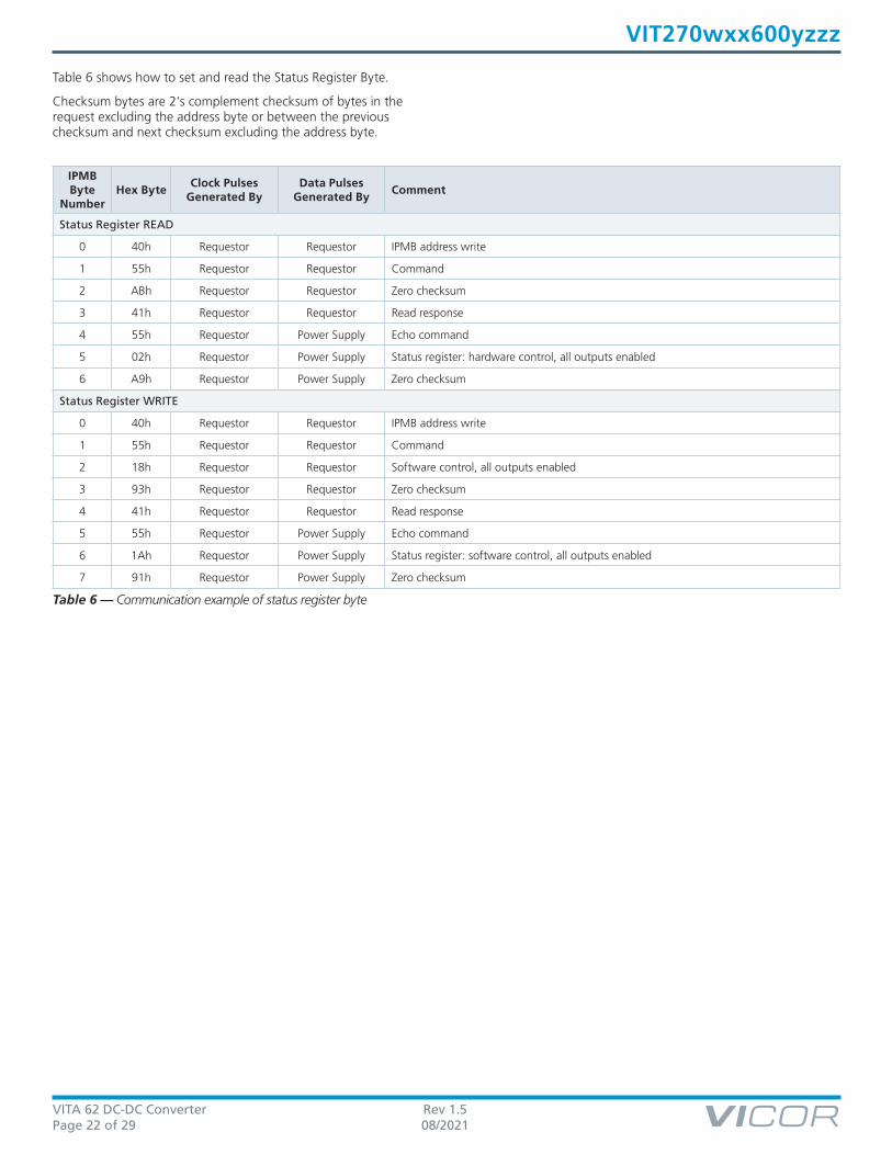
Table 6 shows how to set and read the Status Register Byte.
Checksum bytes are 2's complement checksum of bytes in the request excluding the address byte or between the previous checksum and next checksum excluding the address byte.
IPMB Byte
NumberHex Byte
Clock Pulses Generated By
Data Pulses Generated By
Comment
Status Register READ
0 40h Requestor Requestor IPMB address write
1 55h Requestor Requestor Command
2 ABh Requestor Requestor Zero checksum
3 41h Requestor Requestor Read response
4 55h Requestor Power Supply Echo command
5 02h Requestor Power Supply Status register: hardware control, all outputs enabled
6 A9h Requestor Power Supply Zero checksum
Status Register WRITE
0 40h Requestor Requestor IPMB address write
1 55h Requestor Requestor Command
2 18h Requestor Requestor Software control, all outputs enabled
3 93h Requestor Requestor Zero checksum
4 41h Requestor Requestor Read response
5 55h Requestor Power Supply Echo command
6 1Ah Requestor Power Supply Status register: software control, all outputs enabled
7 91h Requestor Power Supply Zero checksum
Table 6 — Communication example of status register byte
VITA 62 DC-DC Converter Rev 1.5Page 23 of 29 08/2021
VIT270wxx600yzzz
Non-VITA 46.11 Recognized by Power Supply
0x44: Firmware Date (Read Only) [e]
• 22 byte response in ASCII form.
Byte Number
Contents Format Typical Value/Comment
0 0x44 Byte Echo of the command
1 – 20 Date ASCII[20] ‘NOV 28 14:32:54 2018’
21 Zero Checksum ByteSum(Bytes 0:21) mod 256 = 0
0x45: Hardware Address (Read Only) [e]
Byte Number
Contents Format Typical Value/Comment
0 0x45 Byte
1 I2C Address Byte0x23, set by *GA1, *GA0
2 Zero Checksum ByteSum(Bytes 0:2) mod 256 = 0
0x55: Status Command (Read/Write) [e]
Byte Number
Contents Format Typical Value/Comment
0 0x55 Byte
1 Status Byte Byte 0x18 = All outputs ON
2 Zero Checksum ByteSum(Bytes 0:2) mod 256 = 0
0x90: All Voltages in mV (Read Only) [e]
Byte Number
Contents Format Scaling/Comment
0 0x90 Byte Echo of the command
1, 2 +12V SENSE UINT16 10mV/bit
3, 4 +3.3V SENSE UINT16 10mV/bit
5, 6 +5V SENSE UINT16 10mV/bit
7, 8 +3.3VAUX SENSE UINT16 10mV/bit
9, 10 +12VAUX VSENSE UINT16 10mV/bit
11, 12 –12VAUX VSENSE UINT16 –10mV/bit
13, 14 Input Voltage UINT16 10mV/bit
15 Zero Checksum ByteSum(Bytes 0:15) mod 256 = 0
[e] Most-significant bit of each byte is transmitted first. Most-significant byte of UINT16 and UINT32 transmitted first.
Commands Recognized by Power Supply
[d] Most-significant bit of each byte is transmitted first. Most-significant byte of UINT16 and UINT32 transmitted first.
0x21: Sensor Data (Read Only) [d]
Byte Number
Contents Format Scaling
0 0x21 Byte Echo of the command
1 Status Reg ByteSee below, same as used by command 0x55
2, 3 PCBA Temperature °C INT16 16384 = 100°C
4, 5 +12V VSENSE UINT16 16384 = 12.0V
6, 7 +3.3V VSENSE UINT16 16384 = 3.3V
8, 9 +5V VSENSE UINT16 16384 = 5.0V
10, 11 +3.3VAUX VSENSE UINT16 16384 = 3.3V
12, 13 +12VAUX VSENSE UINT16 16384 = 12.0V
14, 15 –12VAUX VSENSE UINT1616384 = –12.0V, absolute value
16, 17 +12V IOUT UINT16 16384 = 40A
18, 19 +3.3V IOUT UINT16 16384 = 20A
20, 21 +5V IOUT UINT16 16384 = 30A
22, 23 +3.3VAUX IOUT UINT16 16384 = 6A
24, 25 +12VAUX IOUT UINT16 16384 = 1A
26, 27 –12VAUX IOUT UINT1616384 = –1A, absolute value
28, 29 INT REFERENCE UINT16 16384 = 2.50V
30, 31 Factory Use Only UINT16 N/A: factory use only
32 – 51 Part Number CHAR[20]no 0 term, padded with 0x20
52 – 55 Serial Number UINT32
Unsigned 32-bit integer; last 9 digits of the serial number of the unit on the label
56, 57 Factory Use Only UINT16 N/A: factory use only
58, 59 Hardware Rev CHAR[2]
60, 61 Firmware Rev CHAR[2]
62 Input Current UINT8 255 = 60A
63 Zero Checksum ByteSum(Bytes 0:63) mod 256 = 0
VITA 62 DC-DC Converter Rev 1.5Page 24 of 29 08/2021
VIT270wxx600yzzz
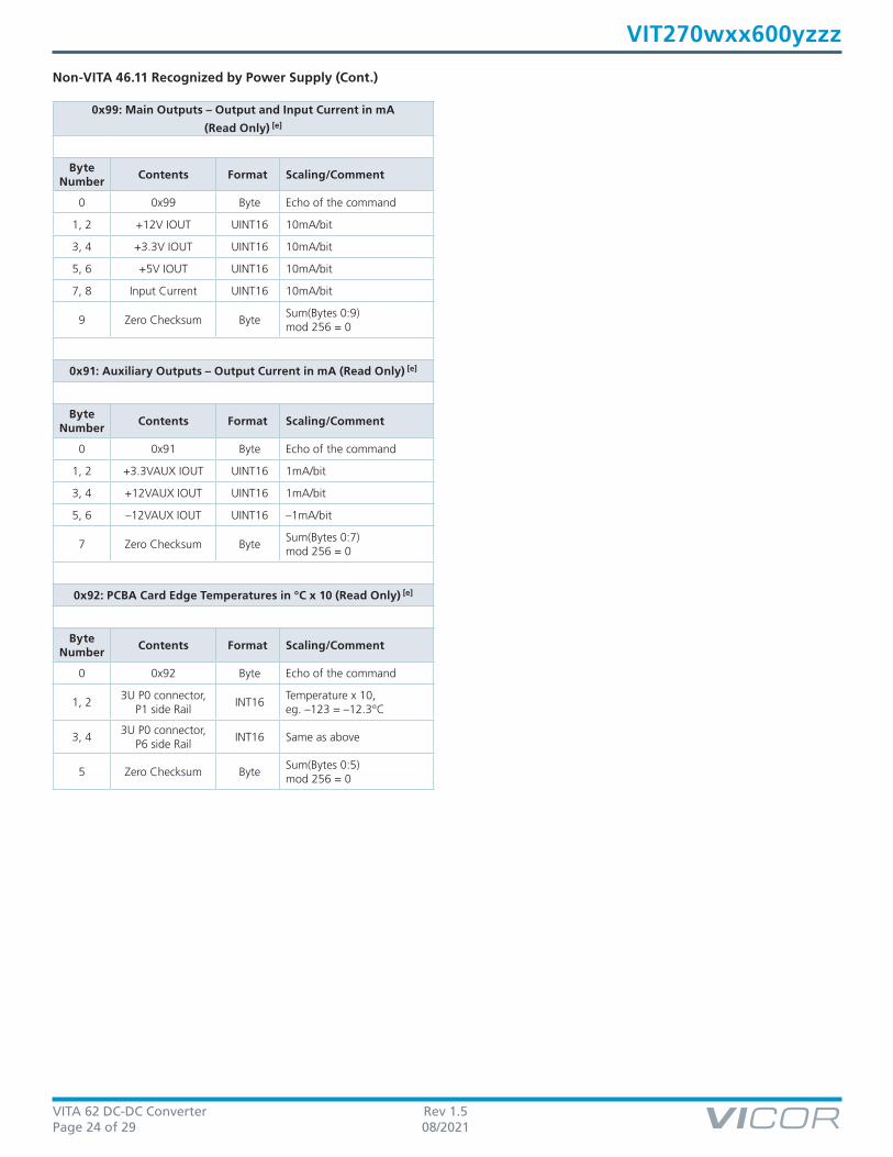
Non-VITA 46.11 Recognized by Power Supply (Cont.)
0x99: Main Outputs – Output and Input Current in mA
(Read Only) [e]
Byte Number
Contents Format Scaling/Comment
0 0x99 Byte Echo of the command
1, 2 +12V IOUT UINT16 10mA/bit
3, 4 +3.3V IOUT UINT16 10mA/bit
5, 6 +5V IOUT UINT16 10mA/bit
7, 8 Input Current UINT16 10mA/bit
9 Zero Checksum ByteSum(Bytes 0:9) mod 256 = 0
0x91: Auxiliary Outputs – Output Current in mA (Read Only) [e]
Byte Number
Contents Format Scaling/Comment
0 0x91 Byte Echo of the command
1, 2 +3.3VAUX IOUT UINT16 1mA/bit
3, 4 +12VAUX IOUT UINT16 1mA/bit
5, 6 –12VAUX IOUT UINT16 –1mA/bit
7 Zero Checksum ByteSum(Bytes 0:7) mod 256 = 0
0x92: PCBA Card Edge Temperatures in °C x 10 (Read Only) [e]
Byte Number
Contents Format Scaling/Comment
0 0x92 Byte Echo of the command
1, 23U P0 connector,
P1 side RailINT16
Temperature x 10, eg. –123 = –12.3°C
3, 43U P0 connector,
P6 side RailINT16 Same as above
5 Zero Checksum ByteSum(Bytes 0:5) mod 256 = 0
VITA 62 DC-DC Converter Rev 1.5Page 25 of 29 08/2021
VIT270wxx600yzzz
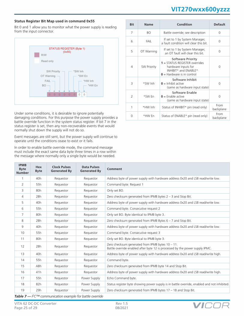
Status Register Bit Map used in command 0x55
Bit 0 and 1 allow you to monitor what the power supply is reading from the input connector.
Under some conditions, it is desirable to ignore potentially damaging conditions. For this purpose the power supply provides a battle override function in the system status register. If bit 7 in the status register is set, then any non-recoverable events that would normally shut down the supply will not do so.
Event messages are still sent, but the power supply will continue to operate until the conditions cease to exist or it fails.
In order to enable battle override mode, the command message must include the exact same data byte three times in a row within the message where normally only a single byte would be needed.
*HW En*HW Inh
*SW En
*SW Inh
BOFAIL
OT Warning
SW Priority
Read only
7 6 5 4 3 2 1 0
0 0 0 0 0 00 0
STATUS REGISTER (Byte 1)(0x55)
R/W
Bit Name Condition Default
7 BO Battle override; see description 0
6 FAILIf set to 1 by System Manager,
a fault condition will clear this bit.0
5 OT WarningIf set to 1 by System Manager, an OT fault will clear this bit.
0
4 SW Priority
Software Priority1 = STATUS REGISTER overrides
hardware inputs for INHIBIT* and ENABLE*
0 = Hardware is in control
0
3 *SW lnhSoftware Inhibit
0 = Inhibit active (same as hardware input state)
0
2 *SW EnSoftware Enable
0 = Enable active (same as hardware input state)
0
1 *HW lnh Status of INHIBIT* pin (read only)From
backplane
0 *HW En Status of ENABLE* pin (read only)From
backplane
IPMB Byte
Number
Hex Byte
Clock Pulses Generated By
Data Pulses Generated By
Comment
1 40h Requestor Requestor Address byte of power supply with hardware address 0x20 and LSB read/write low.
2 55h Requestor Requestor Command byte. Request 1
3 80h Requestor Requestor Only set BO.
4 2Bh Requestor Requestor Zero checksum generated from IPMB bytes 2 – 3 and Stop Bit.
5 40h Requestor Requestor Address byte of power supply with hardware address 0x20 and LSB read/write low.
11 80h Requestor Requestor Only set BO. Byte identical to IPMB byte 3.
12 2Bh Requestor RequestorZero checksum generated from IPMB bytes 10 – 11. Battle override enabled after byte 12 is processed by the power supply IPMC.
13 40h Requestor Requestor Address byte of power supply with hardware address 0x20 and LSB read/write high.
14 55h Requestor Requestor Command byte.
15 ABh Requestor Requestor Zero checksum generated from IPMB byte 14 and Stop Bit.
16 41h Requestor Requestor Address byte of power supply with hardware address 0x20 and LSB read/write high.
17 55h Requestor Power Supply Echo Command byte.
18 82h Requestor Power Supply Status register byte showing power supply is in battle override, enabled and not inhibited.
19 29h Requestor Power Supply Zero checksum generated from IPMB bytes 17 – 18 and Stop Bit.
Table 7 — I2C™ communication example for battle override
VITA 62 DC-DC Converter Rev 1.5Page 26 of 29 08/2021
VIT270wxx600yzzz
Table 8 — Sensor list and coefficients
IPMI Interface
The data interface is compliant with the requirements of VITA 46.11, VITA 62 -2016 and the IPMI v2.0 specifications. This section shows product specific information such as a sensor list and their coefficients.
Data Format
Four constants are used to calculate a real world value from the single byte variable returned in the response. The four constants are used in the equation Interpreting Received Values
Where:
y the converted reading
x the raw sensor reading
M the signed integer multiplier
B the signed additive offset
K1 signed exponent for constant B (sets decimal point for B)
K2 signed result exponent (sets decimal point for y)
Sensors and Constants
The list of sensors and coefficients can also be retrieved by the chassis manager by querying the “Sensor Data Record” (See VITA 46.11).
y = (Mx + (B • 10K1)) • 10K2
Sensor Number
Hex Sensor NameType Code
DescriptionSI
UnitsM B K1 K2
2 02h FRU Health F2h 04h - Predictive Failure Discrete
3 03h FRU Voltage 02h 05h - Limit Exceeded Discrete
4 04h FRU Temperature F3h 6Fh - Sensor Specific Discrete
7 07h Input Voltage Not Supported
8 08h VS1, +12V Voltage 02h
01h - Threshold
V 20 90 2 –3
9 09h VS2, +3.3V Voltage 02h V 10 20 2 –3
10 0Ah VS3, +5V Voltage 02h V 10 35 2 –3
11 0Bh AUX2, +3.3VAUX Voltage 02h V 10 20 2 –3
12 0Ch AUX3, +12VAUX Voltage 02h V 20 90 2 –3
13 0Dh AUX1, –12VAUX Voltage 02h V –20 –90 2 –3
14 0Eh Input Current Not Supported
15 0Fh iS1, +12V Current 03h
01h - Threshold
A 20 0 0 –2
16 10h iS2, +3.3V Current 03h A 20 0 0 –2
17 11h iS3, +5V Current 03h A 20 0 0 –2
18 12h Card Edge Temp towards P6 01h K 1 20 1 0
19 13h Card Edge Temp towards P1 01h K 1 20 1 0
21 15h Input Power Consumption Not Supported
22 16h VS1, +12V Power Consumption 0Bh
01h - Threshold
W 25 0 0 –1
23 17h VS2, +3.3V Power Consumption 0Bh W 4 0 0 –1
24 18h VS3, +5V Power Consumption 0Bh W 10 0 0 –1
25 19h iAUX2, +3.3VAUX Current 03h A 50 0 0 –3
26 1Ah iAUX3, +12VAUX Current 03h A 20 0 0 –3
27 1Bh iAUX1, –12VAUX Current 03h A 20 0 0 –3
28 1Ch AUX Power Consumption 0Bh W 8 0 0 –1
33 21h Output Power Consumption 0Bh W 30 0 0 –1
VITA 62 DC-DC Converter Rev 1.5Page 27 of 29 08/2021
VIT270wxx600yzzz
Table 9 — Sensor thresholds
Thresholds
Upper and lower limits of the sensors are shown in Table 5. Exceeding the nonrecoverable or critical limits will trigger a system event message and set the appropriate bits in the warning sensor registers (Sensors 2, 3 and 4). They reflect a degradation of the power supply towards its operational limits but are still within operating norms.
Exceeding nonrecoverable limits of the power supply will cause the power supply to shut down all outputs except the 3.3V internal supply which powers the microcontroller and bus interface. The system will try to recover from all nonrecoverable faults after 1s shut down of all outputs.
The high non-recoverable threshold of the input voltage is set to 255h (60V) since the unit is capable of operating through MIL-STD-1275E surges. The surge protection circuit inside the power supply will limit the input voltage to be inside the units allowable range during a surge. If a surge exceeding the maximum allowable limits persists, the unit will shut down for at least 25s and attempt auto-recovery.
22 VS1, +12V Power Consumption 192 480W 220 550W 6
23 VS2, +3.3V Power Consumption 165 66W 195 78W 6
24 VS3, +5V Power Consumption 130 130W 172 172W 6
25 iAUX2, +3.3VAUX Current 130 6.5A 165 8.25A 5
26 iAUX3, +12VAUX Current 45 0.9A 70 1.4A 5
27 iAUX1, –12VAUX Current 45 0.9A 70 1.4A 5
28 AUX Power Consumption 123 98.4W 140 112W 5
33 Output Power 192 576W 215 645W 4
VITA 62 DC-DC Converter Rev 1.5Page 28 of 29 08/2021
VIT270wxx600yzzz
Mechanical Drawing
3.937
3.197
6.634
3.335 .301
THERMAL SEATING PLANE
.951
.257
.393
.495 NOMINAL,WEDGE-LOCKEXPANDS TO.545 MAX.
1 2 3
DIMENSION ARE IN INCHES
Connector Components
Item # Description Manufacturer Manufacturer Part Number
1 VITA46 0 DEG Guide Socket TE Connectivity 1-1469492-1
2 VITA62 Connector Plug TE Connectivity 6450849-7
3 VITA46 315 DEG Guide Socket TE Connectivity 1-1469492-8
VITA 62 DC-DC Converter Rev 1.5Page 29 of 29 08/2021
VIT270wxx600yzzz
Revision History
Revision Date Description Page Number(s)
1.0 08/21/18 Initial release n/a
1.1 10/15/18
Updated features & benefits, product descriptionUpdated connector pin descriptionsUpdated current specs for main +3.3V outputUpdated 0x21 tableUpdated command 0x55 table
1361516
1.2 05/30/19Updated output ripple/noise specs for –12V and +12V outputsUpdated MIL-STD-461F CS114 standards compliance to “pass”
614
1.3 08/12/20 Updated terminology 15
1.4 06/30/21
Expanded input voltage rangeRemoved B and 001 optionsAdded signal characteristics, signal pin functions, typical external circuits, card edge temperature sensors, fault operation, parallel operation, standalone operation sectionsUpdated I2C sensor commands sectionUpdated sensor thresholds
1, 54
8 – 9, 14 – 17
21 – 2527
1.5 08/26/21Typo correction for 0x90 Byte 0Updated sensor thresholds for sensors 25 – 28, added sensor 33
2327
Contact Us: http://www.vicorpower.com/contact-us
Vicor Corporation25 Frontage Road
Andover, MA, USA 01810Tel: 800-735-6200Fax: 978-475-6715