Page 1
DEPARTMENT OF ELECTRONICS & INSTRUMENTATION
ENGINEERING
Post-Graduate programme M.Tech.(VLSI & EMBEDDED SYSTEMS)
Rules, Regulations, Scheme of Instruction & Evaluation and Syllabi
KAKATIYA INSTITUTE OF TECHNOLOGY & SCIENCE::
WARANGAL-506015
KAKATIYA UNIVERSITY,WARANGAL
The course structure and scheme of Evaluation (Semester wise) for the
Post-Graduate programme
Page 2
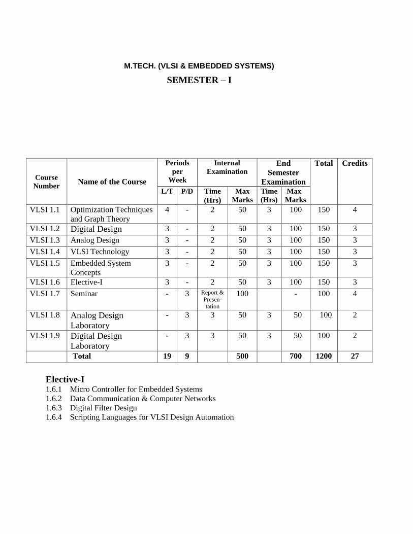
M.TECH. (VLSI & EMBEDDED SYSTEMS)
SEMESTER – I
Course
Number Name of the Course
Periods
per
Week
Internal
Examination End
Semester
Examination
Total Credits
L/T P/D Time
(Hrs)
Max
Marks
Time
(Hrs)
Max
Marks
VLSI 1.1 Optimization Techniques
and Graph Theory
4 - 2 50 3 100 150 4
VLSI 1.2 Digital Design 3 - 2 50 3 100 150 3
VLSI 1.3 Analog Design 3 - 2 50 3 100 150 3
VLSI 1.4 VLSI Technology 3 - 2 50 3 100 150 3
VLSI 1.5 Embedded System
Concepts
3 - 2 50 3 100 150 3
VLSI 1.6 Elective-I 3 - 2 50 3 100 150 3
VLSI 1.7 Seminar - 3 Report &
Presen-
tation
100 - 100 4
VLSI 1.8 Analog Design
Laboratory
- 3 3 50 3 50 100 2
VLSI 1.9 Digital Design
Laboratory
- 3 3 50 3 50 100 2
Total 19 9 500 700 1200 27
Elective-I 1.6.1 Micro Controller for Embedded Systems
1.6.2 Data Communication & Computer Networks
1.6.3 Digital Filter Design
1.6.4 Scripting Languages for VLSI Design Automation
Page 3
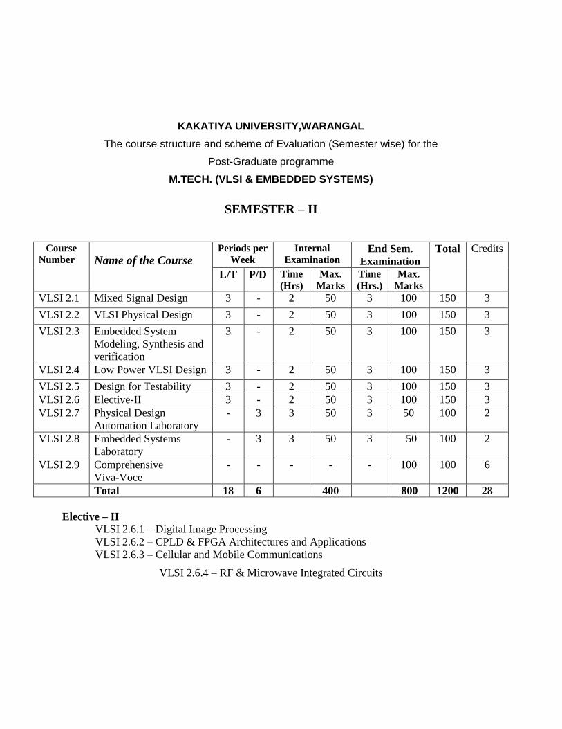
KAKATIYA UNIVERSITY,WARANGAL
The course structure and scheme of Evaluation (Semester wise) for the
Post-Graduate programme
M.TECH. (VLSI & EMBEDDED SYSTEMS)
SEMESTER – II
Course
Number Name of the Course Periods per
Week Internal
Examination End Sem.
Examination
Total Credits
L/T P/D Time
(Hrs) Max.
Marks Time
(Hrs.) Max.
Marks
VLSI 2.1 Mixed Signal Design 3 - 2 50 3 100 150 3
VLSI 2.2 VLSI Physical Design 3 - 2 50 3 100 150 3
VLSI 2.3 Embedded System
Modeling, Synthesis and
verification
3 - 2 50 3 100 150 3
VLSI 2.4 Low Power VLSI Design 3 - 2 50 3 100 150 3
VLSI 2.5 Design for Testability 3 - 2 50 3 100 150 3
VLSI 2.6 Elective-II 3 - 2 50 3 100 150 3
VLSI 2.7 Physical Design
Automation Laboratory
- 3 3 50 3 50 100 2
VLSI 2.8 Embedded Systems
Laboratory
- 3 3 50 3 50 100 2
VLSI 2.9 Comprehensive
Viva-Voce
- - - - - 100 100 6
Total 18 6 400 800 1200 28
Elective – II
VLSI 2.6.1 – Digital Image Processing
VLSI 2.6.2 – CPLD & FPGA Architectures and Applications
VLSI 2.6.3 – Cellular and Mobile Communications
VLSI 2.6.4 – RF & Microwave Integrated Circuits
Page 4
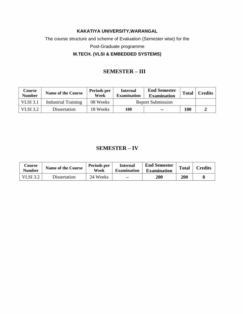
KAKATIYA UNIVERSITY,WARANGAL
The course structure and scheme of Evaluation (Semester wise) for the
Post-Graduate programme
M.TECH. (VLSI & EMBEDDED SYSTEMS)
SEMESTER – III
Course
Number Name of the Course
Periods per
Week Internal
Examination End Semester
Examination Total Credits
VLSI 3.1 Industrial Training 08 Weeks Report Submission
VLSI 3.2 Dissertation 18 Weeks 100 -- 100 2
SEMESTER – IV
Course
Number Name of the Course
Periods per
Week Internal
Examination End Semester
Examination Total Credits
VLSI 3.2 Dissertation 24 Weeks -- 200 200 8
Page 5
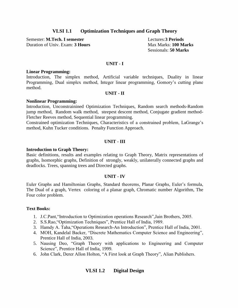
VLSI 1.1 Optimization Techniques and Graph Theory
Semester: M.Tech. I semester Lectures:3 Periods
Duration of Univ. Exam: 3 Hours Max Marks: 100 Marks
Sessionals: 50 Marks
UNIT - I
Linear Programming:
Introduction, The simplex method, Artificial variable techniques, Duality in linear
Programming, Dual simplex method, Integer linear programming, Gomory’s cutting plane
method.
UNIT - II
Nonlinear Programming: Introduction, Unconstrainined Optimization Techniques, Random search methods-Random
jump method, Random walk method, steepest descent method, Conjugate gradient method-
Fletcher Reeves method, Sequential linear programming.
Constrained optimization Techniques, Characteristics of a constrained problem, LaGrange’s
method, Kuhn Tucker conditions. Penalty Function Approach.
UNIT - III
Introduction to Graph Theory:
Basic definitions, results and examples relating to Graph Theory, Matrix representations of
graphs, Isomorphic graphs, Definition of strongly, weakly, unilaterally connected graphs and
deadlocks. Trees, spanning trees and Directed graphs.
UNIT - IV
Euler Graphs and Hamiltonian Graphs, Standard theorems, Planar Graphs, Euler’s formula,
The Dual of a graph, Vertex coloring of a planar graph, Chromatic number Algorithm, The
Four color problem.
Text Books:
1. J.C.Pant,“Introduction to Optimization operations Research”,Jain Brothers, 2005.
2. S.S.Rao,“Optimization Techniques”, Prentice Hall of India, 1989.
3. Hamdy A. Taha,“Operations Research-An Introduction”, Prentice Hall of India, 2001.
4. MOH, Kandelal Backer, “Discrete Mathematics Computer Science and Engineering”,
Prentice Hall of India, 2003.
5. Nausing Deo, “Graph Theory with applications to Engineering and Computer
Science”, Prentice Hall of India, 1999.
6. John Clark, Derer Allon Holton, “A First look at Graph Theory”, Alian Publishers.
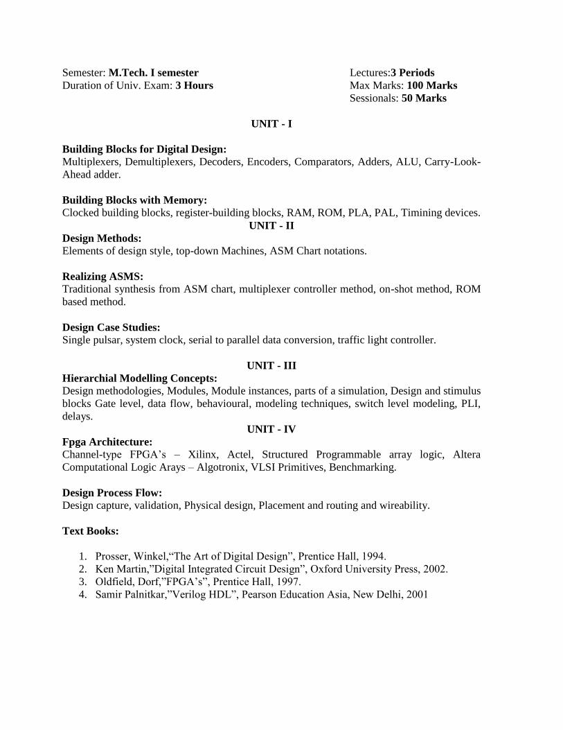
VLSI 1.2 Digital Design
Page 6
Semester: M.Tech. I semester Lectures:3 Periods
Duration of Univ. Exam: 3 Hours Max Marks: 100 Marks
Sessionals: 50 Marks
UNIT - I
Building Blocks for Digital Design: Multiplexers, Demultiplexers, Decoders, Encoders, Comparators, Adders, ALU, Carry-Look-
Ahead adder.
Building Blocks with Memory: Clocked building blocks, register-building blocks, RAM, ROM, PLA, PAL, Timining devices.
UNIT - II
Design Methods: Elements of design style, top-down Machines, ASM Chart notations.
Realizing ASMS: Traditional synthesis from ASM chart, multiplexer controller method, on-shot method, ROM
based method.
Design Case Studies: Single pulsar, system clock, serial to parallel data conversion, traffic light controller.
UNIT - III
Hierarchial Modelling Concepts:
Design methodologies, Modules, Module instances, parts of a simulation, Design and stimulus
blocks Gate level, data flow, behavioural, modeling techniques, switch level modeling, PLI,
delays.
UNIT - IV
Fpga Architecture: Channel-type FPGA’s – Xilinx, Actel, Structured Programmable array logic, Altera
Computational Logic Arays – Algotronix, VLSI Primitives, Benchmarking.
Design Process Flow: Design capture, validation, Physical design, Placement and routing and wireability.
Text Books:
1. Prosser, Winkel,“The Art of Digital Design”, Prentice Hall, 1994.
2. Ken Martin,”Digital Integrated Circuit Design”, Oxford University Press, 2002.
3. Oldfield, Dorf,”FPGA’s”, Prentice Hall, 1997.
4. Samir Palnitkar,”Verilog HDL”, Pearson Education Asia, New Delhi, 2001
Page 7
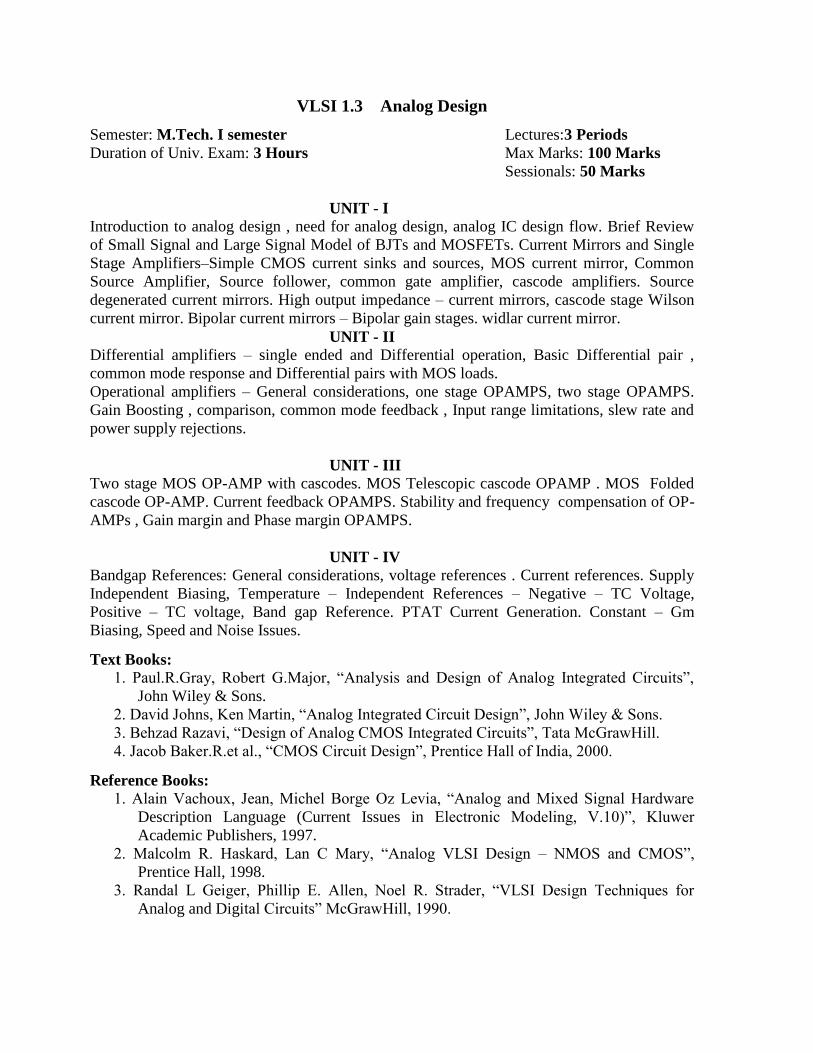
VLSI 1.3 Analog Design
Semester: M.Tech. I semester Lectures:3 Periods
Duration of Univ. Exam: 3 Hours Max Marks: 100 Marks
Sessionals: 50 Marks
UNIT - I
Introduction to analog design , need for analog design, analog IC design flow. Brief Review
of Small Signal and Large Signal Model of BJTs and MOSFETs. Current Mirrors and Single
Stage Amplifiers–Simple CMOS current sinks and sources, MOS current mirror, Common
Source Amplifier, Source follower, common gate amplifier, cascode amplifiers. Source
degenerated current mirrors. High output impedance – current mirrors, cascode stage Wilson
current mirror. Bipolar current mirrors – Bipolar gain stages. widlar current mirror.
UNIT - II
Differential amplifiers – single ended and Differential operation, Basic Differential pair ,
common mode response and Differential pairs with MOS loads.
Operational amplifiers – General considerations, one stage OPAMPS, two stage OPAMPS.
Gain Boosting , comparison, common mode feedback , Input range limitations, slew rate and
power supply rejections.
UNIT - III
Two stage MOS OP-AMP with cascodes. MOS Telescopic cascode OPAMP . MOS Folded
cascode OP-AMP. Current feedback OPAMPS. Stability and frequency compensation of OP-
AMPs , Gain margin and Phase margin OPAMPS.
UNIT - IV
Bandgap References: General considerations, voltage references . Current references. Supply
Independent Biasing, Temperature – Independent References – Negative – TC Voltage,
Positive – TC voltage, Band gap Reference. PTAT Current Generation. Constant – Gm
Biasing, Speed and Noise Issues.
Text Books:
1. Paul.R.Gray, Robert G.Major, “Analysis and Design of Analog Integrated Circuits”,
John Wiley & Sons.
2. David Johns, Ken Martin, “Analog Integrated Circuit Design”, John Wiley & Sons.
3. Behzad Razavi, “Design of Analog CMOS Integrated Circuits”, Tata McGrawHill.
4. Jacob Baker.R.et al., “CMOS Circuit Design”, Prentice Hall of India, 2000.
Reference Books:
1. Alain Vachoux, Jean, Michel Borge Oz Levia, “Analog and Mixed Signal Hardware
Description Language (Current Issues in Electronic Modeling, V.10)”, Kluwer
Academic Publishers, 1997.
2. Malcolm R. Haskard, Lan C Mary, “Analog VLSI Design – NMOS and CMOS”,
Prentice Hall, 1998.
3. Randal L Geiger, Phillip E. Allen, Noel R. Strader, “VLSI Design Techniques for
Analog and Digital Circuits” McGrawHill, 1990.
Page 8
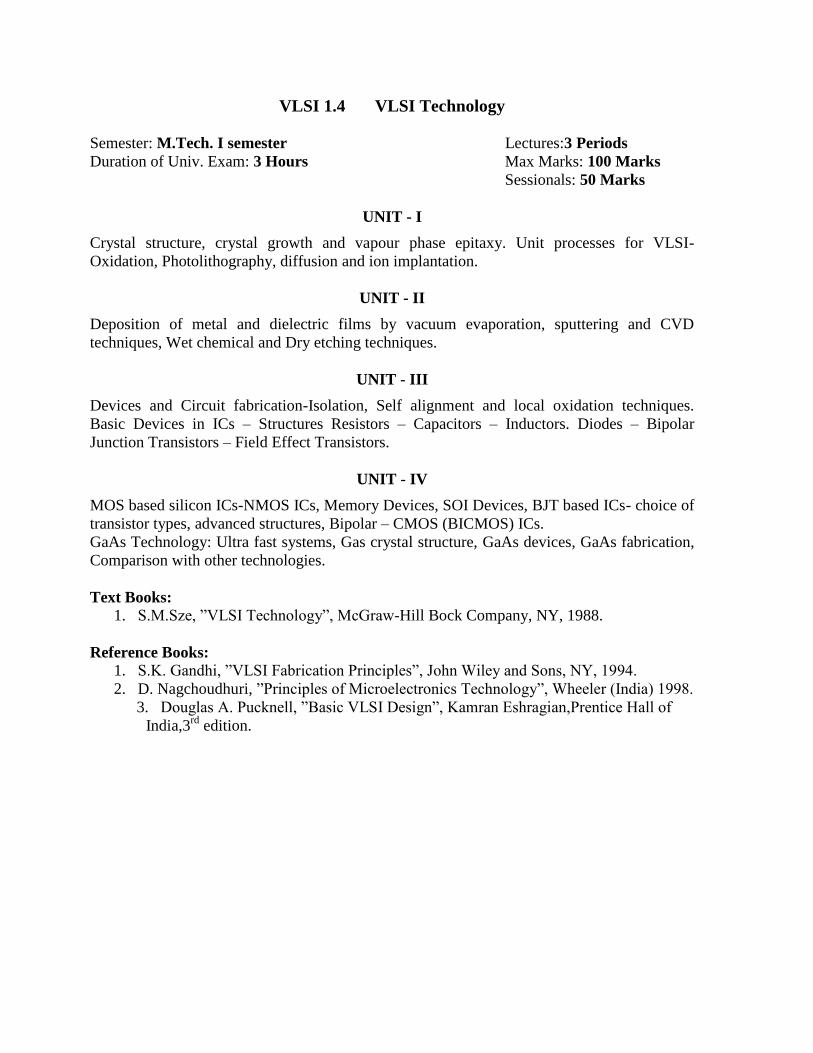
VLSI 1.4 VLSI Technology
Semester: M.Tech. I semester Lectures:3 Periods
Duration of Univ. Exam: 3 Hours Max Marks: 100 Marks
Sessionals: 50 Marks
UNIT - I
Crystal structure, crystal growth and vapour phase epitaxy. Unit processes for VLSI-
Oxidation, Photolithography, diffusion and ion implantation.
UNIT - II
Deposition of metal and dielectric films by vacuum evaporation, sputtering and CVD
techniques, Wet chemical and Dry etching techniques.
UNIT - III
Devices and Circuit fabrication-Isolation, Self alignment and local oxidation techniques.
Basic Devices in ICs – Structures Resistors – Capacitors – Inductors. Diodes – Bipolar
Junction Transistors – Field Effect Transistors.
UNIT - IV
MOS based silicon ICs-NMOS ICs, Memory Devices, SOI Devices, BJT based ICs- choice of
transistor types, advanced structures, Bipolar – CMOS (BICMOS) ICs.
GaAs Technology: Ultra fast systems, Gas crystal structure, GaAs devices, GaAs fabrication,
Comparison with other technologies.
Text Books:
1. S.M.Sze, ”VLSI Technology”, McGraw-Hill Bock Company, NY, 1988.
Reference Books: 1. S.K. Gandhi, ”VLSI Fabrication Principles”, John Wiley and Sons, NY, 1994.
2. D. Nagchoudhuri, ”Principles of Microelectronics Technology”, Wheeler (India) 1998.
3. Douglas A. Pucknell, ”Basic VLSI Design”, Kamran Eshragian,Prentice Hall of
India,3rd
edition.
Page 9
VLSI 1.5 Embedded System Concepts
Semester: M.Tech. I semester Lectures:3 Periods
Duration of Univ. Exam: 3 Hours Max Marks: 100 Marks
Sessionals: 50 Marks
UNIT - I
Introduction to Embedded Systems:
Characteristics, Different Types of Embedded Systems, Components of Embedded System,
Hardware Architecture, Processor, Peripheral Devices, Embedded Software Architecture,
Need of Real Time Operating Systems and Different Application Areas.
Processor and Memory Selection:
Different Types of Processor Technologies, Processor Selection for an Embedded
System, Different Types of Memory Devices, Memory Selection for an Embedded System.
UNIT-II
Communication Interfacing: Communication protocol concepts, Microprocessor
interfacing: I/O addressing, Port and Bus based, I/O, Memory Mapped I/O, Standard I/O
interrupts, Direct memory access, Serial Communication Protocols I2C, CAN, Parallel
Communication Protocols PCI bus, PCI-X and Wireless protocol IrDA, blue tooth.
Device Drivers and Interrupts Servicing Mechanism: Different types of Interrupts, Interrupt Servicing Mechanism, Device Servicing using ISR,
Device Drivers, Parallel Port and Serial Port Device Drivers and Device driver Programming
UNIT - III
Software Engineering Practices in the Embedded Software Development Process:
Software Development Life Cycle and its Models, Real Time Programming Issues during
the Software Development Process.
Embedded Software Programming: Assembly Language, C, C++ and Java
Programming models for Single and Multiprocessor Systems: DFG, CDFG
FSM, Petrinets, SDFG, HSDF, APEG and MTG
UNIT-IV
Real Time Operating Systems
Basics of Operating Systems, Differences between General Purpose and Real-Time
Operating Systems, Features of Real Time Operating Systems,RTOS Kernel Structure,
Issues in multitasking– task assignment, scheduling, InterProcess Communication and
Synchronization, Interrupt routines in RTOS Environment and Real Time Task Scheduling.
Commercial Real-Time Operating Systems: uCOS-II, RTLinux, LYNXOS, PSOS,
QNX//Neutrino, VX Works
Text Books:
1. Raj Kamal, “Embedded Systems”, Tata McGraw Hill, 2003.
2. Frankvahid/Tony Givargis, “Embedded System Design- A Unified
Hardware/software Introduction”.
3. Real Time Systems, Jane W.S. LIU., Pearson Education, Asia, 2001.
4. Dream Tech Software Team, “Programming Embedded Systems”, John Wiley Pub,
2004.
Page 10
Reference Books:
1.C.M. Krishna and G. Shin, “. Real Time Systems” Mc Graw-Hill International
Editions,1997.
2Daniel W.Lewis, “Fundamentals of Embedded Software-where C and Assembly meet”,
Pearson Education, 2002
Page 11
VLSI 1.6.1 Micro Controllers for Embedded Systems
Semester: M.Tech. I semester Lectures:3 Periods
Duration of Univ. Exam: 3 Hours Max Marks: 100 Marks
Sessionals: 50 Marks
UNIT - I
Introduction to Embedded Systems:
Review of Microprocessors and their Features. 8 & 16 Bit Micro Controller Families (of Intel
8051 & 8097; Motorola 68HC11; Micro Chips PIC 16C6X & 16C7X) and Micro controller
hardware. Brief ideas on Embedded RISC Processor Architectures –ARM7TDMI/
ARM9TDMI/10TDMI (Advanced RISC Machines Limited’s) and Motorola 680HX
Processor IP Cores, their Features for Embedded Applications.
UNIT - II
Micro Controller Interfacing:
Using 8051, 68HC11 & PIC-16C7X - External Memory Interfacing – Memory Management
Unit, Instruction and data cache, memory controller. On Chip Counters, Timers, Serial I/O,
Interrupts and their use.
Software Development:
Modular Software development, Layered software systems. Product Design Cycle, Challenges
in Embedded System Design and system partitioning, Programming model, exception
handling and processing. Device drivers, Object oriented interfacing. Threads and Interfacing
methods.
UNIT - III
Programming: Instruction sets and assembly language program concepts and programming the 8051,
68HC11, PIC-16C7X Micro controllers & ARM7TDMI Core.
Interrupt synchronization – Interrupt vectors & priority, external interrupt design. Threads –
Multi threaded preemptive scheduler & semaphores. Serial I/O Devices - RS232
Specifications, RS422/Apple Talk/RS 423/RS435 & other communication protocols. Serial
communication controller - UART, HDLC.
UNIT – IV
Ethernet Protocol, SDMA, Channels and IDMA Simulation, CPM Interrupt Controller and
CPM Timers, power controls, External BUS Interface system Development and Debugging.
Case Studies: Design of Embedded Systems using the micro controllers - 8051/ARM7TDMI, for
applications in the area of Communications, Automotives.
Text Books:
Page 12
1. M.A. Mazadi, J.G. Mazidi, “The 8051 Micro Controller & Embedded Systems”, Pearson
Education, Asia 2000.
2. John B. Peatman, “Designing with PIC Micro Controllers”, Pearson Education.
3. Jonathan W. Valvano, “Embedded Microcomputer systems, Real Time Interfacing”,
Brookes/Cole, Thomas learning, 1999.
4. S. Fuber, “ARM System on – Chip Architecture”, 2nd
Edition, Addison Wesley, Great
Briton, 2000.
Reference Books:
1. Frank Vahid, Tony Givargis, Embedded System Design, “A Unified Hardware/Software
Introduction”, John Wiley and Sons, Asia pvt. Ltd., 2002.
2. Kenneth Hintz, Danial Tabak, “Micro controllers Architecture, Implementation &
Programming”, McGraw Hill, 1992.
3. Arnold Berger, “Embedded System Design: An Introduction to Processes, Tools and
Techniques”, CMP Books 2001.
4. Wayne Wolf, “Computers as Components: Principles of Embedded Computer System
Design”, Morgan-Kaufman, 2000.
5. Motorola, “ The Programming Environment for 32 bit ps – Motorola MPC 860 manual,
Motorola Inc.
6. Cathey May and Silha (Ed), “The Power PC Architecture”, Morgan Kauffman Press,1998.
7. Craig Hollabaugh, Embedded Linux, Hardware, Software and Interfacing, Pearson
Education.
8. Daniel W. Lewis, “Fundamentals of Embedded Software, Where C and Assembly Meet”,
Pearson Education.
Page 13
VLSI 1.6.2 Data Communications and Computer Networks
Semester: M.Tech. I semester Lectures:3 Periods
Duration of Univ. Exam: 3 Hours Max Marks: 100 Marks
Sessionals: 50 Marks
UNIT - I
Introduction to Network components, switching technologies, topologies, transmission media,
protocols & routing.
WAN, NAN, LAN. Queuing theory models and applications computer networks, Data
communication concepts – asynchronous & synchronous transmission, error correction codes
& detectors.
UNIT - II
Transmission Protocols: STOP – START, BSC, SDLC, HDLC, Retransmission techniques. LAN – components,
Topologies, Access techniques, IEEE 802 standards, switched and Fast Ethernet, FDDI &
SONET.
UNIT - III
Network Protocols – concepts, layers, Architecture, OSI model – X.25, TCP/IP layers –
addressing & routing in an Internet, Major application layers, near services: a mail, w.w.w.,
F.T.P., Telnet. Backbone networks / Inter-networking – Devices: Switches, Hubs, Bridges,
routers, gateways and choice for implementation.
UNIT - IV
Broad band Networks – ISDN, ATM, Protocol. Quality of service & Traffic management
concepts, VSAT Networks. Brief ideas on network security and management.
Text Books:
1. Black. U, “Computer Networks, Protocols, Standards and Interfaces”, Prentice Hall of
India 1997.
2. Tahenbanm S.A., “Computer Networks”, Prentice Hall of India, 1996.
3. Stalling W., “High Speed Networks: TCP/IP and ATM Design principles”, Prentice
Hall of India, 1998.
Reference Books:
1. Shanmugam A, Rajeev S, “Computer Communication Networks”, ISTE learning
material center, 2001.
2. Stalling. W, “ISDN and Broadband ISDN with Frame Relay and ATM”,3rd
Edition,
Prentice Hall of India, 1998.
3. Charles.P.Pleegar, “Security in Computing”, Prentice Hall of India, 1998.
Page 14
VLSI 1.6.3 Digital Filter Design
Semester: M.Tech. I semester Lectures:3 Periods
Duration of Univ. Exam: 3 Hours Max Marks: 100 Marks
Sessionals: 50 Marks
UNIT - I
Multirate Digital Signal Processing:
Introduction – Decimation by integer factor. Interpolation by an integer factor. Sampling rate
conversion by non-integer factors. Multistage approach to sampling rate conversion. Design
of practical sampling-rate converters. Software implementation of interpolators and
decimators. Sample rate conversion using polyphase filter structure. Examples of applications
of multirate DSP.
UNIT - II
Linear Prediction and Optimum Linear Filters:
Representation of a stationary random process. Rational power spectra-A. R, M.A & ARMA
processes. Relationship between the filter parameters and Auto-correlation sequence.
Forward and Backward linear prediction
UNIT - III
Optimum reflection coefficients for the Lattice forward and backward predictors. A.R.
process and linear prediction. Solution of Normal equations. Levinson-Durbin algorithm.
The Schur algorithm. Pipelined architecture for implementing the Schur algorithm
UNIT - IV
Properties of Linear Prediction error filters. AR Lattice and ARMA Lattice-Ladder filters.
Wiener filters for filtering and prediction. Orthogonality principle in Linear Mean-Square
Estimation.
Text Books:
1. E.C. Ifeachor et.al., “Digital Signal Processing” Pearson Education Asia Publication,
2nd
Edn. (2002).
2. John G.Proakis, C.M. Radar et.al., “Algorithms for Statistical Signal Processing” by
Pearson Education Asia Publication, 2nd
Edn. (2002).
Reference Books
Dimitris G. Manolakis et.al., “Statistical & Adaptive Signal Processing”, Mc.
GrawHill International Edn. (2000).
VLSI 1.6.4 Scripting Languages for VLSI Design Automation
Page 15
Semester: M.Tech. I semester Lectures:3 Periods
Duration of Univ. Exam: 3 Hours Max Marks: 100 Marks
Sessionals: 50 Marks
UNIT - I
Overview of Scripting Languages-PERL, CGI, VB Script, Java Script.
UNIT - II
PERL: Operators, Statements Pattern Matching etc. Data Structures, Modules, Objects, Tied
Variables.
UNIT - III
Inter process Communication Threads, Compilation & Line Interfacing.
UNIT - IV
Debugger Internal & Externals Portable Functions. Extensive Exercises for Programming in
PERL.
Other Languages:
Broad Details of CGI, VB Script, Java Script with Programming Examples.
Text Books:
1. Randal L, Schwartz Tom Phoenix, “Learning PERL”.
2. Larry Wall, Tom Christiansen, John Orwant, “Programming PERL”.
Page 16
VLSI 1.7 Seminar
Class : M.Tech I Semester Practicals: 1 Period
Internal Examination: 100 Marks
Note: Each student has to give independent seminars on the topics covering the following:
1. A Seminar Topic covering the state-of-the-art technical topics relevant up to the
second Semester theory subjects, which would supplement and complement the
programme are to be assigned to each student.
Guidelines:
1. The Students of M.Tech. I semester are to register a relevant topic with in 4 weeks of
commencement of semester class work and submit the same to the department.
2. Evaluation of seminar consists of two components namely Report (50 marks) and
Presentation (50 marks)
(a) Report: Students are required to submit a report on the chosen seminar topic as per
the prescribed format and last date specified by the Departmental Post Graduate
Review Committee (DPGRC)
(b) Presentation: The students are required to deliver the seminar before the DPGRC
as per the schedule notified by the department.
DPGRC will decide the course of action on the students who fail to submit the report
and present the seminar.
Page 17
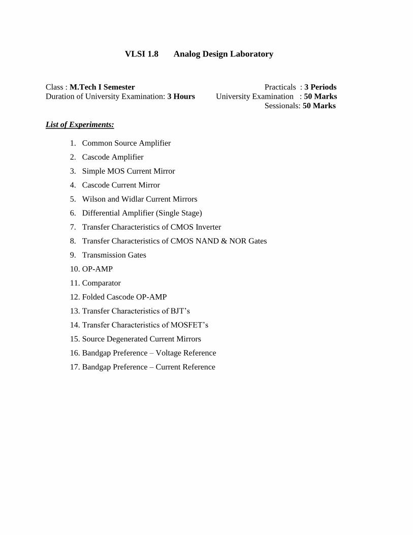
VLSI 1.8 Analog Design Laboratory
Class : M.Tech I Semester Practicals : 3 Periods
Duration of University Examination: 3 Hours University Examination : 50 Marks
Sessionals: 50 Marks
List of Experiments:
1. Common Source Amplifier
2. Cascode Amplifier
3. Simple MOS Current Mirror
4. Cascode Current Mirror
5. Wilson and Widlar Current Mirrors
6. Differential Amplifier (Single Stage)
7. Transfer Characteristics of CMOS Inverter
8. Transfer Characteristics of CMOS NAND & NOR Gates
9. Transmission Gates
10. OP-AMP
11. Comparator
12. Folded Cascode OP-AMP
13. Transfer Characteristics of BJT’s
14. Transfer Characteristics of MOSFET’s
15. Source Degenerated Current Mirrors
16. Bandgap Preference – Voltage Reference
17. Bandgap Preference – Current Reference
Page 18
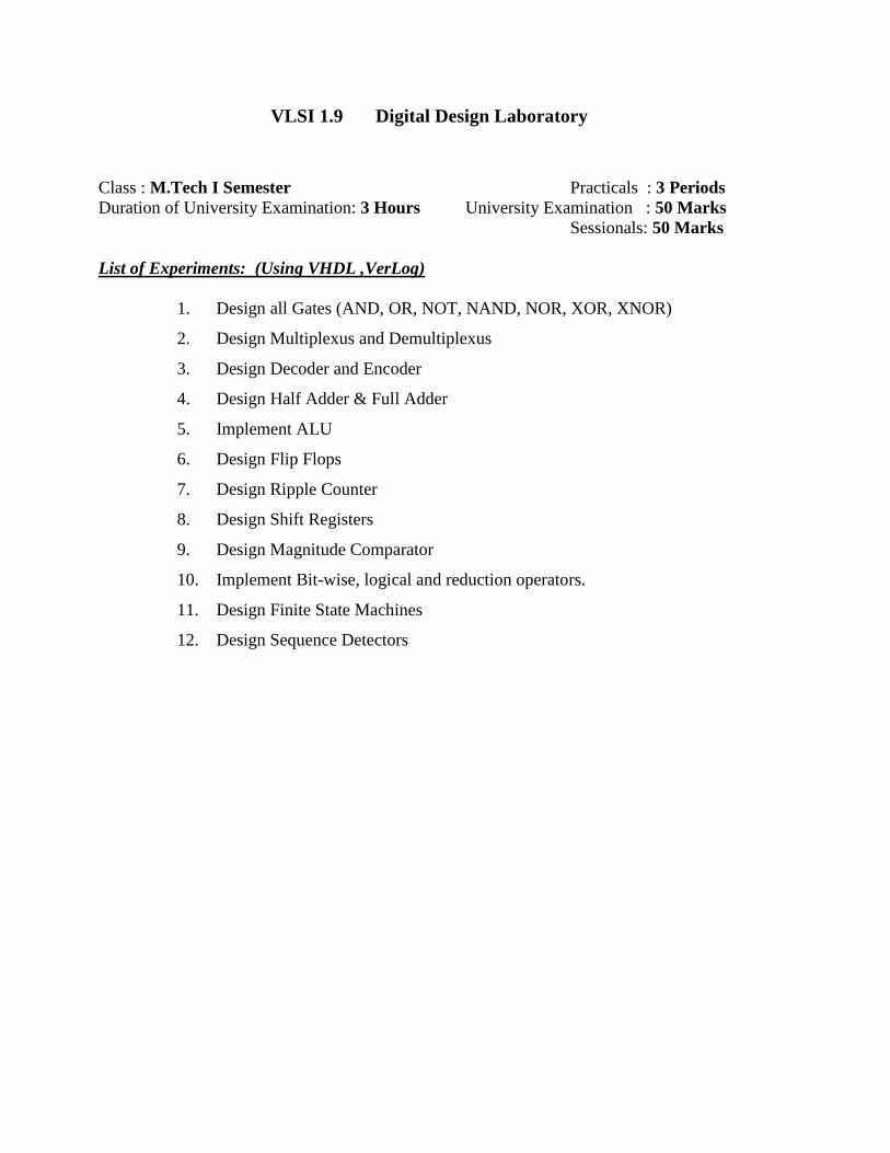
VLSI 1.9 Digital Design Laboratory
Class : M.Tech I Semester Practicals : 3 Periods
Duration of University Examination: 3 Hours University Examination : 50 Marks
Sessionals: 50 Marks
List of Experiments: (Using VHDL ,VerLog)
1. Design all Gates (AND, OR, NOT, NAND, NOR, XOR, XNOR)
2. Design Multiplexus and Demultiplexus
3. Design Decoder and Encoder
4. Design Half Adder & Full Adder
5. Implement ALU
6. Design Flip Flops
7. Design Ripple Counter
8. Design Shift Registers
9. Design Magnitude Comparator
10. Implement Bit-wise, logical and reduction operators.
11. Design Finite State Machines
12. Design Sequence Detectors
Page 19
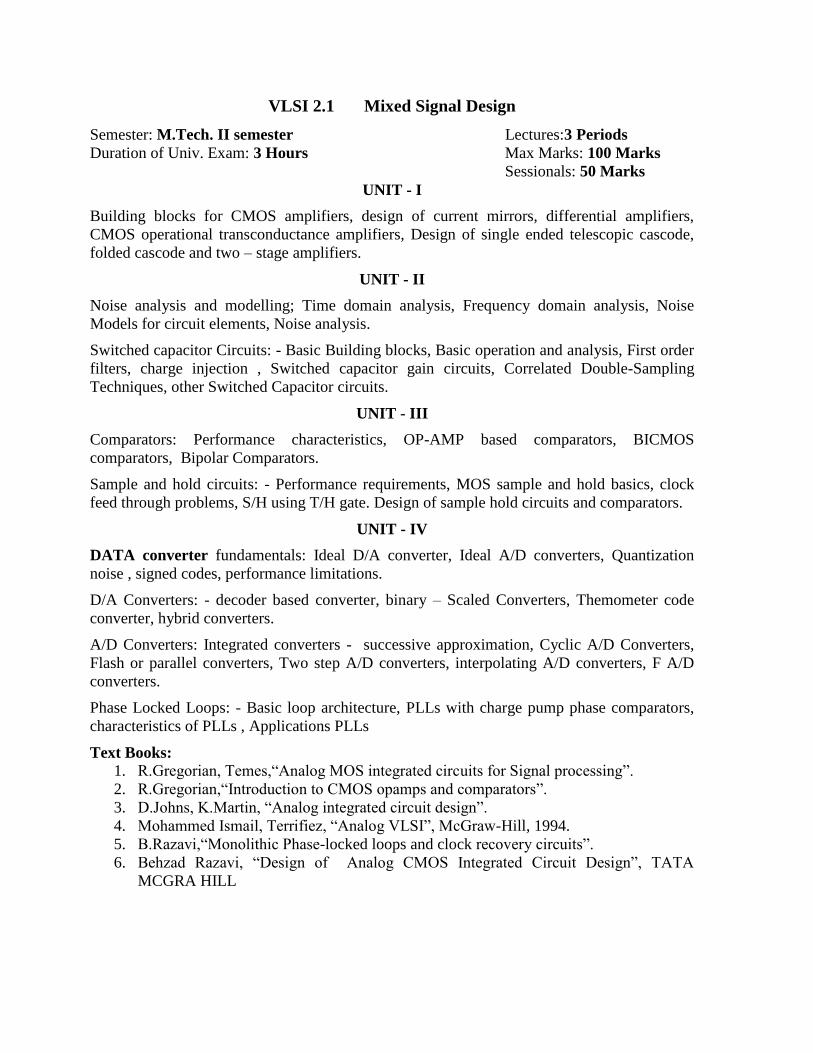
VLSI 2.1 Mixed Signal Design
Semester: M.Tech. II semester Lectures:3 Periods
Duration of Univ. Exam: 3 Hours Max Marks: 100 Marks
Sessionals: 50 Marks
UNIT - I
Building blocks for CMOS amplifiers, design of current mirrors, differential amplifiers,
CMOS operational transconductance amplifiers, Design of single ended telescopic cascode,
folded cascode and two – stage amplifiers.
UNIT - II
Noise analysis and modelling; Time domain analysis, Frequency domain analysis, Noise
Models for circuit elements, Noise analysis.
Switched capacitor Circuits: - Basic Building blocks, Basic operation and analysis, First order
filters, charge injection , Switched capacitor gain circuits, Correlated Double-Sampling
Techniques, other Switched Capacitor circuits.
UNIT - III
Comparators: Performance characteristics, OP-AMP based comparators, BICMOS
comparators, Bipolar Comparators.
Sample and hold circuits: - Performance requirements, MOS sample and hold basics, clock
feed through problems, S/H using T/H gate. Design of sample hold circuits and comparators.
UNIT - IV
DATA converter fundamentals: Ideal D/A converter, Ideal A/D converters, Quantization
noise , signed codes, performance limitations.
D/A Converters: - decoder based converter, binary – Scaled Converters, Themometer code
converter, hybrid converters.
A/D Converters: Integrated converters - successive approximation, Cyclic A/D Converters,
Flash or parallel converters, Two step A/D converters, interpolating A/D converters, F A/D
converters.
Phase Locked Loops: - Basic loop architecture, PLLs with charge pump phase comparators,
characteristics of PLLs , Applications PLLs
Text Books:
1. R.Gregorian, Temes,“Analog MOS integrated circuits for Signal processing”.
2. R.Gregorian,“Introduction to CMOS opamps and comparators”.
3. D.Johns, K.Martin, “Analog integrated circuit design”.
4. Mohammed Ismail, Terrifiez, “Analog VLSI”, McGraw-Hill, 1994.
5. B.Razavi,“Monolithic Phase-locked loops and clock recovery circuits”.
6. Behzad Razavi, “Design of Analog CMOS Integrated Circuit Design”, TATA
MCGRA HILL
Page 20
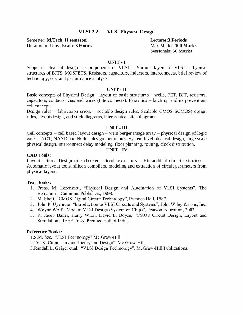
VLSI 2.2 VLSI Physical Design
Semester: M.Tech. II semester Lectures:3 Periods
Duration of Univ. Exam: 3 Hours Max Marks: 100 Marks
Sessionals: 50 Marks
UNIT - I Scope of physical design – Components of VLSI – Various layers of VLSI – Typical
structures of BJTS, MOSFETS, Resistors, capacitors, inductors, interconnects, brief review of
technology, cost and performance analysis.
UNIT - II Basic concepts of Physical Design - layout of basic structures – wells, FET, BJT, resistors,
capacitors, contacts, vias and wires (Interconnects). Parasitics – latch up and its prevention,
cell concepts.
Design rules – fabrication errors – scalable design rules. Scalable CMOS SCMOS) design
rules, layout design, and stick diagrams, Hierarchical stick diagrams.
UNIT - III
Cell concepts – cell based layout design – wein berger image array – physical design of logic
gates – NOT, NAND and NOR – design hierarchies. System level physical design, large scale
physical design, interconnect delay modeling, floor planning, routing, clock distribution.
UNIT - IV
CAD Tools: Layout editors, Design rule checkers, circuit extractors – Hierarchical circuit extractors –
Automatic layout tools, silicon compilers, modeling and extraction of circuit parameters from
physical layout.
Text Books:
1. Preas, M. Lorenzatti, “Physical Design and Automation of VLSI Systems”, The
Benjamin – Cummins Publishers, 1998.
2. M. Shoji, “CMOS Digital Circuit Technology”, Prentice Hall, 1987.
3. John P. Uyemura, “Introduction to VLSI Circuits and Systems”, John Wiley & sons, Inc.
4. Woyne Wolf, “Modern VLSI Design (System on Chip)”, Pearson Education, 2002.
5. R. Jacob Baker, Harry W.Li., David E. Boyce, “CMOS Circuit Design, Layout and
Simulation”, IEEE Press, Prentice Hall of India.
Reference Books:
1.S.M. Sze, “VLSI Technology” Mc Graw-Hill.
2.“VLSI Circuit Layout Theory and Design”, Mc Graw-Hill.
3.Randall L. Geiger et.al., “VLSI Design Technology”, McGraw-Hill Publications.
Page 21
VLSI 2.3 Embedded System Design Modeling, Synthesis and Verification
Semester: M.Tech. II semester Lectures:3 Periods
Duration of Univ. Exam: 3 Hours Max Marks: 100 Marks
Sessionals: 50 Marks
UNIT-I
Introduction: System-Design Challenges, Abstraction Levels, System Design Methodology,
System- Level Models, Platform Design, System Design Tools
System Level Design Methodologies: Bottom-up Methodology, Top-down Methodology,
Meet-in-the-middle Methodology, Platform Methodology, FPGA Methodology, System-level
Synthesis, Processor Synthesis
UNIT-II
Modeling: Models of Computation, System Design Languages, System Modeling, Processor
Modeling, Communication Modeling, Speciation Model, Network TLM, Protocol TLM Bus
Cycle-Accurate Model, Cycle-Accurate Model
System Synthesis: System Design Trends, TLM Based Design, Automatic TLM Generation,
Automatic Mapping, Platform Synthesis
UNIT-III
Software Synthesis: Preliminaries, Target Languages for Embedded Systems, RTOS,
Software Synthesis Overview from TLM, Code Generation, Multi-Task Synthesis, Internal
Communication, External Communication Start up Code, Binary Image Generation,
Execution
Hardware Synthesis: RTL Architecture, Input Models, Estimation and Optimization,
Register Sharing, Functional Unit Sharing, Connection Sharing, Register Merging, Chaining
and Multi-Cycling, Functional-Unit Pipelining, Data path Pipelining, Control and Data path
Pipelining, Scheduling, Interface Synthesis
UNIT-IV
Verification: Simulation Based Methods, Formal Verification Methods, Comparative
Analysis of Verification Methods, System Level Verication
A Unified Embedded Co- design Methodology using UML and SystemC
Refined design methodology, SystemC 2.0, UML 2.0 Diagrams, UML Profile for SystemC,
Modeling and generating test cases for Transactional Level SystemC design
Text Book
1. Embedded System Design Modeling, Synthesis and Verification, Gajski, D.D;
Abdi,S;Gerstlauer,A;Schirner,G;,Springer publications, ISBN:978-1-4419-0503-1
2. J.Basker,“A SystemC Primer”, Star Galaxy Publishing, 2002.
Reference Book
1. Frankvahid/Tony Givargis, “Embedded System Design- A Unified
Hardware/software Introduction”.
Page 22
VLSI 2.4 Low Power VLSI Design
Semester: M.Tech. II semester Lectures:3 Periods
Duration of Univ. Exam: 3 Hours Max Marks: 100 Marks
Sessionals: 50 Marks
UNIT - I
Introduction and need of low power design sources of power dissipation and design strategies
for low power. Physics of power dissipation in CMOS-low power VLSI design limits. Power
estimation at circuit level – modeling of signals, signal probability calculations, statistical
techniques, input vector compaction, circuit reliability. Synthesis for low power – behaviour
level transforms, logic and circuit level optimization.
UNIT – II Design styles and testing – low voltage CMOS circuit design styles, leakage current in deep
submission transitions and design issues, minimization of short channel effects (SCE) and hot
carrier effects. Testing of deep sub micron ICs with elevated intrinsic leakage.
UNIT - III Low power architectures – MOS static RAM cells, banked organization SRAMS, reducing
voltage swing on bit lines, write lines, driver circuits and sense amplifier circuits. Energy
computing and recovery techniques – energy dissipation using an RC model, energy recovery
circuit design, design with partially reversible logic and supply clock generation.
UNIT - IV
Software design for low power - dedicated hardware Vs software implementation, power
dissipation, estimation and optimization. Automated power code generation and co design for
low power.
Text Books:
1. Kaushik Roy, Sharad Prasad, “Low Power CMOS VLSI Circuit Design”, John Wiley
& Sons, 2000.
2. A.P. Chandrakasan, R.W. Broderson, “Low Power design”, IEEE Press, 1998.
3. J.B. Kuo, J.H. Juo, “Low Voltage VLSI Circuits”, John Wiley & Sons.
Page 23
VLSI 2.5 Design for Testability
Semester: M.Tech. II semester Lectures:3 Periods
Duration of Univ. Exam: 3 Hours Max Marks: 100 Marks
Sessionals: 50 Marks
UNIT - I
Introduction to Test and Design fro Testability (DFT) Fundamentals.
Modeling: Modeling digital circuits at logic level, register level and structural models. Levels of
modeling. Logic Simulation: Types of simulation, Delay models, Element evaluation, Hazard
detection, Gate level event driven simulation. Fault Modeling – Logic fault models, Fault
detection and redundancy, Fault equivalence and fault location. Single stuck and multiple
stuck – Fault models. Fault simulation applications, General techniques for Combinational
circuits.
UNIT - II
Testing for single stuck faults (SSF) – Automated test pattern generation (ATPG/ATG) for
SSFs in combinational and sequential circuits, Functional testing with specific fault models.
Vector simulation – ATPG vectors, formats, Compaction and compression, Selecting ATPG
Tool.
UNIT - III
Design for testability – testability trade-offs, techniques. Scan architectures and testing –
controllability and absorbability, generic boundary scan, full integrated scan, storage cells for
scan design. Board level and system level DFT approaches. Boundary scan standards.
Compression techniques – different techniques, syndrome test and signature analysis.
UNIT - IV Built-in self-test (BIST) – BIST Concepts and test pattern generation. Specific BIST
Architectures – CSBL, BEST, RTS, LOCST, STUMPS, CBIST, CEBS, RTD, SST, CATS,
CSTP, BILBO. Brief ideas on some advanced BIST concepts and design for self-test at board
level.
Memory BIST (MBIST): Memory test architectures and techniques – Introduction to memory test, Types of memories
and integration, Embedded memory testing model. Memory test requirements for MBIST.
Brief ideas on embedded core testing.
Text Books:
1. Miron Abramovici, Melvin A. Breur, Arthur D. Friedman, “Digital Systems Testing
and Testable Design”, Jaico Publishing House, 2001.
2. Alfred Crouch, “Design for Test for Digital ICs & Embedded Core Systems”, Prentice
Hall.
3. Robert J. Feugate, Jr., Steven M. Mentyn, “Introduction to VLSI Testing”, Prentice
Hall, 1998.
Page 24
VLSI 2.6.1 Digital Image Processing
Semester: M.Tech. II semester Lectures:3 Periods
Duration of Univ. Exam: 3 Hours Max Marks: 100 Marks
Sessionals: 50 Marks
UNIT - I
Introduction:
Fundamental Steps in Digital Image Processing, Components of an Image Processing System.
Digital Image Fundamentals:
Elements of Visual Perception, Image Sensing and Acquisition, Image Sampling and
Quantization, Basic Relationships between Pixels
UNIT - II
Image Enhancement in the Spatial Domain:
Some Basic Gray Level Transformations, Histogram Processing, Enhancement Using
Arithmetic/Logic Operations, Basics of Spatial Filters.
Image Enhancement Sharpening Spatial Filters. Domain in the Frequency:
An Introduction to the Fourier Transform and the Frequency Domain, Smoothing Frequency -
Domain Filters, Sharpening Frequ4ency Domain Filters, Implementation.
UNIT - III
Image Restoration:
Noise Models, Restoration in the Presence of Noise Only-Spatial Filtering, Periodic Noise
Reduction by Frequency Domain Filtering, Linear Position - Invariant Degradations
Estimating the degradation Function, Inverse Filtering, Minimum Mean square Error filtering,
Geometric Mean Filter and Transformations.
Image Compression: Fundamentals, Image Compression Models, Elements of Information Theory, Error-Free
Compression, Lossy Compression, Image Compression Standards.
UNIT - IV
Image Segmentation:
Detection of Discontinuities, Edge Linking and Boundary Detection, Thresholding, Region
Based Segmentation, Segmentation by Morphological Watersheds, The Use of Motion in
Segmentation.
Representation and Description:
Representation, Boundary Descriptions, Regional descriptors.
Text Books:
1. Rafael C.Gonzalez, Richard E.Woods, “Digital Image Processing”, Pearson Education,
Second Edition, 2002.
VLSI 2.6.2 CPLD and FPGA Architectures and Applications
Page 25
Semester: M.Tech. II semester Lectures:3 Periods
Duration of Univ. Exam: 3 Hours Max Marks: 100 Marks
Sessionals: 50 Marks
UNIT - I
Programmable Logic: Read Only Memory (ROM), Programmable Logic Array (PLA)/Programmable Array Logic
(PAL). Sequential Programmable Logic Devices (PLDs). Programmable Gate Arrays (PGAs)
– Features, Programming and applications using Complex Programmable Logic Devices
(CPLDs) - Altera series – Max 5000/7000 Series and ALTERA FLEX Logic – 10000 Series
CPLDs. AMD’s – CPLD (Mach 1 to 5); Cypres FLASH 370 Device Technology, Lattice
pLSI’s Architectures – 3000 Series – Speed Performance and in system programmability.
FPGAs: Field Programmable Gate Arrays – Logic blocks, routing architecture, Design flow,
Technology Mapping for FPGAs, Case studies – Xilinx XC4000 & ALTERA’s FLEX
8000/10000 FPGAs: AT & T – ORCA’s (Optimized Reconfigurable Cell Array): ACTEL’s –
ACT-1, 2, 3 and their speed performance.
UNIT - II
Finite State Machines (FSM): Top Down Design - State Transition Table, state assignments for FPGAs. Problem of initial
state assignment for one hot encoding. Derivations of state machine charts. Realization of
state machine charts with a PAL. Alternative realization for state machine chart using
microprogramming. Linked state machines. One – Hot state machine, Petrinetes for state
machines – basic concepts, properties. Extended petrinetes for parallel controllers. Finite State
Machine – Case Study, Meta Stability, Synchronization. HDL Simulation Using
VHDL/Verilog – Different Descriptions, Simulation Cycles, Process, Loops, Delay models,
Library functions, Procedures, Synthesis, Test bench.
UNIT - III
FSM Architectures and Systems Level Design: Architectures centered around non-registered PLDs. State machine designs centered around
shift registers. One – Hot design method. Use of ASMs in One – Hot design. Application of
One – Hot method. System level design – controller, data path and functional partition. PLD:
SPLDs, Programming, Applications - Case Studies using MAX 7000, Design flow, Timing.
Place And Root (PAR)
UNIT - IV
Page 26
Digital Front End Digital Design Tools for FPGAs & ASICs: Using Mentor Graphics EDA Tool (“FPGA Advantage”) - Design Flow Using FPGAs -
Guidelines and Case Studies of parallel adder cell, parallel adder sequential circuits, counters,
multiplexers, parallel controllers.
Text Books:
1. P.K. Chan, S. Mourad, “Digital Design Using Field Programmable Gate Array”, Prentice
Hall, 1994.
2. S. Trimberger, “Field Programmable Gate Array Technology”, Kluwer Academic
Publications, 1994.
3. J. Old Field, R. Dorf, “Field Programmable Gate Arrays”, John Wiley and Sons,
Newyork, 1995.
4. S. Brown, R. Francis, J. Rose, Z.Vransic, “Field Programmable Gate array”, Kluwer
Academic Publication, 1992.
Reference Books:
1. The Programmable Logic Data Books, Xilinx, 1994.
2. PLD & FPGAs from Xilinx, Altera, AMD.
Page 27
VLSI 2.6.3 Cellular and Mobile Communications
Semester: M.Tech. II semester Lectures:3 Periods
Duration of Univ. Exam: 3 Hours Max Marks: 100 Marks
Sessionals: 50 Marks
UNIT - I
Introduction to Cellular Mobile Systems: Operation performance and planning of cellular-analog and digital systems. System design-
concepts of frequency reuse, Co-channel interference reduction, Hand-off mechanism, Cell
splitting & Components of cellular system.
UNIT - II
Co-channel Interference, Real time interference & reduction, Power measurement at mobile
receiver and service area calculations, and interference between systems. Frequency
management: Spectrum utilization, channel, co-channel assignment and call blocking
algorithms.
UNIT - III
Hand-off and dropped calls queuing and introduction to dropped cell rate. Review of digital
communication techniques-ARQ techniques, Digital speech & multiple access schemes for
mobile telephonic.
UNIT - IV
Digital Cellular Systems: Important concepts of - GSM, TDMA, CDMA, PDC, DECT, CDPD, PCN and PCS Systems.
CDMA cellular radio networks, brief ideas on intelligent networks for wireless
communication - AIN, SS7, ISDN, FPLMTS and ATM Networks.
Text Books:
1. William C.Y. Lee, “Mobile Cellular Telecommunications-Analog Digital Systems”,
2nd
Edition, Mc Graw Hill, 2001.
2. Mike Gallagher, Randy Snyder, “Mobile Telecommunication Networks with IS 41”,
Mc Graw Hill, 1997.
Reference Books
1. William C.Y. Lee, “Mobile Communication Engineering”, McGraw Hill, 2001.
Page 28
VLSI 2.6.4 RF and Microwave Integrated Circuits
Semester: M.Tech. II semester Lectures:3 Periods
Duration of Univ. Exam: 3 Hours Max Marks: 100 Marks
Sessionals: 50 Marks
UNIT - I Analysis and design of RF and microwave lines – Review of transmission lines, parallel plate
transmission line, low frequency solution, high frequency solution, strip line and micro strip
transmission lines, low frequency solution, high frequency properties of microslot line, co
planer wave guides, coupled microstrip lines, spiral inductors – capacitors.
UNIT - II
Microstrip / Stripline based filters. Resonators, phase shifters, micro strip based gyrators,
circulators and isolators, directional couplers.
UNIT - III
Microwave active devices – microwave transistors, Gaas FETS (Structures, equivalent
circuit), Low noise amplifiers, power amplifiers, oscillators, detectors, mixers, modulators and
switches.
UNIT - IV
Technology of MICS: Deposition techniques – vacuum evaporation – Vacuum sputtering ion
plating, MBE (Molecular Beam Epitaxy) – photo lithography, mask preparation, thick film
technology, GaAs technology. MIC Packaging: Component attachment, bonding techniques,
solder reflow techniques, input/output terminations, testing.
Text Books:
1. I. Kneppo, J. Fabian, ”Microwave Integrated Circuit”, London: Chapman & Hall,
1994.
2. M. W. Medley, “Microwave and RF Circuit: Analysis, Synthesis and Design”, Artech
House, 1993.
3. R. Goyal, “Monolithic Microwave Integrated Circuits: Technology & Design”, Artech
House, 1989.
4. R.E. Collin, “Foundations for Microwave Engineering”, McGrawHill Publications,
1992.
Reference Books:
1. Y. Konishi, “Microwave Integrated Circuit”, Dekker, New York: Marcel Dekker,
1991.
2. I. Kasa, “Microwave Integrated Circuit”, Elsevier, 1991.
Page 29
VLSI 2.7 Physical Design Automation Laboratory
Class : M.Tech II Semester Practicals : 3 Periods
Duration of University Examination: 3 Hours University Examination : 50 Marks
Sessionals: 50 Marks
List of Experiments:
1. Layout of Basic Devices
2. Partitioning Algorithms
3. Place and Route Algorithms
4. Floor Planning and Pin Assignment
5. Routing
6. Clock distribution
7. Interconnect Delay modeling
8. Modeling and Extraction of circuit parameters from Physical layout.
9. Automatic layout tools
10. Silicon Compilers.
11. Design rule checkers.
Page 30
VLSI 2.8 Embedded Systems Laboratory
Class: M.Tech II Semester Practicals: Periods
Duration of University Examination: 3 Hours University Examination : 50 Marks
Sessionals: 50 Marks
List of Experiments:
1. Design All Basic Logic Gates Using SystemC
2. Design Finite State Machines and Sequence Detector Using SystemC
3. Simple Bus Model using SystemC
4. System level Modeling and Design using UML 2.0 Profile
i. Composite Structure Diagrams
ii. Interaction Overview Diagrams
iii. Sequence Diagrams
iv. State hart Diagrams
v. Timing Diagrams
vi. Class Diagrams
vii. Code Generation from Class Diagrams and State hart Diagrams
5. Implementing IPC Mechanisms using SystemC
6. Serial Communication Programming
7. Writing Device Drivers
8. RTOS Programming
Page 31
VLSI 3.1 Industrial Training
Class : M.Tech III Semester
Guidelines for Industrial Training:
1. M.Tech. Coordinator in consultation with the Training & Placement
section has to procure training-cum-dissertation slots, for the students
before the last day of instruction of II semester.
2. The students are to confirm their training slot by the last day of II
semester.
3. The students after 8 weeks of Industrial Training shall submit a
certificate, and the last date specified and a report in prescribed format
by the DPGRC.
The DPGRC will decide the course of action on the students who fail to
submit the training certificate and report.
Page 32
VLSI 3.1 Industrial Training
Class : M.Tech III Semester
Guidelines for Industrial Training:
4. M.Tech. Coordinator in consultation with the Training & Placement
section has to procure training-cum-dissertation slots, for the students
before the last day of instruction of II semester.
5. The students are to confirm their training slot by the last day of II
semester.
6. The students after 8 weeks of Industrial Training shall submit a
certificate, and the last date specified and a report in prescribed format
by the DPGRC.
The DPGRC will decide the course of action on the students who fail to
submit the training certificate and report.
Page 33
VLSI 3.2 Dissertation
Class : M.Tech IV Semester
Guidelines for Dissertation :
The Department Post-Graduate Review committee is to be constituted with 5
members i.e. Chairman – Head of the Department, Convenor – M.Tech. Coordinator
and 3 other faculty members including supervisor.
The committee is to evaluate the progress of the Dissertation conducting 2
presentations in third semester and monthly presentations in fourth semester.
III – Semester Total Marks – 100
50 marks for presentations
50 marks for regular evaluation by supervisor.
1st presentation (Registration Seminar) after 6 weeks from the commencement of
the semester for 25 marks
2nd
presentation (Progress Seminar) after 12 weeks from the commencement of the
semester for 25 marks
Registration Seminar : Project proposal (problem specification, expected out come)
IV – Semester Total Marks – 200
Progress Seminar : Status of the dissertation – work already carried out, balance of
work to be carried out – Progress seminars are to be carried out every month between
1st and 5
th.
Synopsis Seminar: Together with synopsis a presentation to be made and the
dissertation should be demonstrated two weeks before the submission date.
Supervisors are to evaluate the Dissertation regularly, based on the progress report
submitted by the students in every week and the same should be recorded.
Project work will be carried out in III and IV semesters under the supervision of a
faculty member from within the respective department. Students may be permitted to
work under the joint guidance of two members of the faculty – in which case, one of
the guides may be from an allied department.
A student may, however, be permitted by the Head of the Department concerned to
work on a project in an Industrial / Research organization, in the project semesters. In
Page 34
such case, the faculty guiding the student shall be called the internal guide and the
scientist / manager guiding, the student (at site) shall be called the external guide.
No student will be allowed to submit the project report before 48 weeks and after 52
weeks from commencement of III semester.
The DPGRC will decide the course of action on the students who fail to submit the
dissertation.