tcvlsi.org VLSI Circuits and Systems Letter Volume 1, Issue 1, April 2015 Founding Editorial Features • Anirban Sengupta and Vipul Kumar Mishra, A Methodology for Comprehensive Schedule Delay Estimation during Design space Exploration in Architectural Synthesis • David Pan, Standard Cell Pin Access Planning and Regular Routing for Self-Aligned Double Patterning Opinions • Yier Jin, Hardware Security: Past, Current, and Future • Theocharis Theocharides, Intelligent Embedded Systems: Trends and Opportunities • Prasun Ghosal and Mayukh Sarkar, Beyond Silicon: Is DNA Computer Going to be the Future? • Amlan Ganguly, Naseef Mansoor and Md Shahriar Shamim, New Frontiers in Wireless Network-on-Chip Designs • Chen Zhuo, Emerging Technologies at Post-CMOS Era Updates • Upcoming conferences and workshops • Call for papers and proposals • Funding Opportunities • Job Openings Outreach and Community Call for Contributions
Transcript
tcvlsi.org
VLSI Circuits and Systems Letter
Volume 1, Issue 1, April 2015
Founding Editorial
Features • Anirban Sengupta and Vipul Kumar Mishra, A Methodology for Comprehensive Schedule Delay Estimation
during Design space Exploration in Architectural Synthesis • David Pan, Standard Cell Pin Access Planning and Regular Routing for Self-Aligned Double Patterning
Opinions • Yier Jin, Hardware Security: Past, Current, and Future • Theocharis Theocharides, Intelligent Embedded Systems: Trends and Opportunities • Prasun Ghosal and Mayukh Sarkar, Beyond Silicon: Is DNA Computer Going to be the Future? • Amlan Ganguly, Naseef Mansoor and Md Shahriar Shamim, New Frontiers in Wireless Network-on-Chip
Designs • Chen Zhuo, Emerging Technologies at Post-CMOS Era
Updates • Upcoming conferences and workshops • Call for papers and proposals • Funding Opportunities • Job Openings
Outreach and Community
Call for Contributions
1
VLSI Circuits and Systems Letter Volume 1 – Issue 1 April 2015
Founding Editorial
The continuous scaling of integrated circuit (IC) technologies has been driving the semiconductor industry for several decades. Nowadays, even though the scaling of mainstream CMOS technologies is starting to slow down, the field of VLSI circuits and systems continues its remarkable growth with numerous opportunities along two complementary avenues: (1) development of post-silicon devices, circuits and systems (e.g., carbon nanotube, graphene, memristor, etc.), and (2) discovery of emerging application domains (e.g., biomedical electronics, internet of things, etc.). The VLSI Circuits and Systems Letter, published twice a year, aims to report recent advances in VLSI technology, education and opportunities and, consequently, grow the research and education activities in the area.
This letter is affiliated with the Technical Committee on VLSI (TCVLSI) under the IEEE Computer Society. TCVLSI covers the design methodologies for advanced VLSI circuit and systems, including digital circuits and systems, analog and radio-frequency circuits, as well as mixed-signal circuits and systems. The emphasis of TCVLSI falls on integrating the design, computer-aided design, fabrication, application, and business aspects of VLSI while encompassing both hardware and software.
TCVLSI sponsors a number of premium conferences and workshops, including, but not limited to, ASAP, ASYNC, ISVLSI, IWLS, SLIP, and ARITH. Emerging research topics and state-of-the-art advances on VLSI circuits and systems are reported at these events on a regular basis. Best paper awards are selected at these conferences to promote the high-quality research work each year. In addition to these research activities, TCVLSI also supports a variety of educational activities related to TCVLSI. Several student travel grants are sponsored by TCVLSI in the following meetings: ASAP 2015, ISVLSI 2015, IWLS 2015, and SLIP 2015. Funds are provided to compensate student travels to these meetings as well as attract more student participation. The organizing committees of these meetings undertake the task of selecting right candidates for these awards.
This issue of the VLSI Circuits and Systems Letter showcases the state-of-the-art developments covering several emerging areas: hardware security, intelligent embedded system, DNA computer, wireless network-on-chip, design for manufacturability, etc. Professional articles are solicited from technical experts to provide an in-depth review of these areas. The articles can be found in the sections of “Features” and “Opinions”. In the section of “Updates”, upcoming conferences/workshops (including their call for papers), funding opportunities and job openings are summarized. Finally, a dedicated section of “Outreach and Community” discusses the motivations and approaches for K-20 education.
We would like to express our great appreciation to all Associate Editors (Mike Borowczak, Prasun Ghosal, Shiyan Hu and Helen Li) for their dedicated effort and strong support in organizing this letter. We are thankful to our web chair Mike Borowczak, for his professional service to make the letter publically available on the Internet. We wish to thank Anirban Sengupta, Vipul Kumar Mishra, David Z. Pan, Yier Jin, Theocharis Theocharides, Prasun Ghosal, Mayukh Sarkar, Amlan Ganguly, Naseef Mansoor, Md Shahriar Shamim and Cheng Zhuo who have contributed their professional articles to this issue. Finally, please allow us to welcome all of you to the founding issue of the Circuits and Systems Letter from TCVLSI. We hope that you will have an enjoyable moment when reading the letter! The call for contributions for the next issue is available at the end of this issue and we encourage you to submit articles, news, etc. to an associate editor covering that scope.
Saraju Mohanty
Chair TCVLSI and Editor University of North Texas
Xin Li TCVLSI Editor
Carnegie Mellon University.
2
VLSI Circuits and Systems Letter Volume 1 – Issue 1 April 2015
Features
A Methodology for Comprehensive Schedule Delay Estimation during Design space Exploration in Architectural Synthesis Anirban Sengupta and Vipul Kumar Mishra Department of Computer Science and Engineering, Indian Institute of Technology, Indore, India
Abstract – This letter presents a novel improved delay estimation methodology during scheduling in high level synthesis (HLS) for application specific computing. In general during delay estimation from scheduling during HLS, only functional unit delay is considered. However for current generation of complex digital systems, interconnects (switching elements) also play a very vital role in effective delay evaluation. Thus consideration of interconnect/storage delay during delay estimation from scheduling during HLS becomes very significant, as inaccurate delay estimation inevitably misguides the exploration process during HLS. Motivating from this fact, this letter proposes an improved schedule delay estimation methodology divided into two phases: (a) process of identifying the operations that contribute to the effective delay of the operation chaining based scheduling (b) process of estimating schedule delay considering delay of interconnect (multiplexer unit) and storage elements (latches and final output register) besides regular functional units (FU). The proposed approach more comprehensively estimates the schedule delay than existing practice. Our results on various benchmarks confirm that proposed approach yields estimated delay more comprehensively (reported later) than current standard practice.
1. Introduction During optimization of design architecture in HLS, accurate estimation of schedule delay is highly significant. Thus,
comprehensively estimating the schedule delay during design space exploration process in HLS leads to high quality design with better precision. As the current technology has moved into deep submicron range, the interconnect delay has started playing a major role in overall system delay. Thus considering interconnect delay becomes extremely important during a comprehensive schedule delay estimation while making design tradeoff evaluation (i.e. in design space exploration (DSE) in high level synthesis). The process of DSE maintains tradeoff between conflicting parameters such as power/area and delay during exploration and is expected to generate an optimal solution as final output based on the user constraints. Therefore the comprehensive delay estimation process during scheduling plays pivotal role during DSE process [1, 2, 3]. Lack of all-encompassing schedule delay estimation process may lead to sub-optimal solution as result of exploration which may not be actually satisfying the delay constraint of the user. Therefore, delay estimation after allocation and binding (which considers interconnect delay) gives more realistic estimate of schedule delay than evaluating delay by only considering FU. Owing to the aforesaid motivations, a novel algorithm that considers interconnect delay during DSE in HLS is proposed in this letter. This letter presents a novel schedule delay estimation method that is more comprehensive and yields a value that is more realistic measure of the delay of the datapath. The contribution of the letter as follows: a) a novel algorithm for more accurate delay estimation after allocation and binding process which considers the impact of multiplexer and latches delay during delay calculation; b) considering size (complexity) of multiplexer during DSE process as operational delay of multiplexers increase with size of the multiplexer (i.e. operation delay of 4: 1 multiplexer is generally greater than 2: 1 multiplexer).
2. Related Work A very rich literature is available on DSE in HLS, however, none of the previous work aimed at incorporating
interconnect and storage element delay during schedule delay estimation. Some authors have considered interconnect delay while describing the timing sequence of the controller for its register transfer level (RTL) circuit however not during scheduling (and thereby not during DSE) [3,4,5,8]. In addition, a genetic algorithm (GA) based DSE methodology was presented in [3, 5] which did not consider mux, demux and latch delay during delay evaluation of scheduling (only considered functional unit during schedule delay estimation however, considered interconnect/storage element besides
3
VLSI Circuits and Systems Letter Volume 1 – Issue 1 April 2015
functional unit during area calculation). Moreover, in [4], suggested a time constrained scheduling based on GA technique. The function of list decoder has been made to decode a chromosome encode by permutation of operations into a valid schedule. The drawback of the model is that it did not consider the impact of allocation and binding in the delay estimation (ignoring interconnect units). The execution time model therefore did not consider interconnect & storage (such as mux, demux, and latch) element delay which plays a substantial role due to large resource sharing during binding in HLS. Moreover in [1], only functional unit during delay estimation was considered during DSE. Furthermore, the authors in [6, 7] have also not considered interconnects during delay evaluation/estimation.
Figure 1: The general flow is shown for our proposed approach.
3. Proposed Approach Schedule delay estimation through the proposed approach is performed in two phases as shown in Figure 1. The
proposed approach is valid for operation chaining based scheduling technique. The first phase is identification of the operations which participate in effective delay estimation. The effective contribution to delay is only made by those operations that do not lie within the lifetime of the other larger delay operations i.e. operations that lie (or overlap) within the lifetime of the other larger delay operations are ignored and do not effectively contribute in the delay estimation. Therefore, the output of the first phase produces a list L[k] containing the operations that effectively contribute to the delay. The second phase calls the list L[k] operation wise to comprehensively estimate schedule delay with consideration of interconnect and storage elements delays of those corresponding operations. Detailed description of the algorithms is given in subsequent sub-sections. For the sake of demonstration of the proposed approach, the scheduled CDFG with chaining/multicycling of JPEG benchmark with resource constraints 1 (+), 2(*) is used, as shown in Figure 2.
A. Operation Identification The proposed algorithm for operation identifier is given in Figure 3. The input of the algorithm is a scheduled CDFG
(based on resource constraints). After taking the input, the algorithm traverses entire scheduled CDFG control step by step to produce the list of operations (which is responsible for effective delay contribution) and the overlapping control steps that occurs between operations which effectively contribute to the delay. In step 3, algorithm determines the number of operation starting in the current control step and then decides to jump to any of the following three conditions: (a) if n=1 (Step 4); (b) if n>1 (step 5); (c) if n=0 (step 6).
Let us demonstrate with an example. First, according to step 3, the value of ‘n’ is determined. (a) If n = 1 then the algorithm jumps to step 4 which directly adds the respective operation to list L[k] and adds its
corresponding CSdelay(Oi) to update the CS count. (Note that the definition of the variables is provided in Figure3.) More specifically, say in Figure 2 at CS14 only one operation (opn 2) is starting (i.e. n=1). Therefore the algorithm jumps to step 4 and directly adds CS of opn 2 (which is CS14) to update the CS count. Further opn 2 is added into the list L[k].
Final realistic schedule delayInput Block
L [k] CSoverlap
Methodology for Operation Identifier contributing to
effective delay
Method for comprehensive schedule delay estimation
Allocation and Binding information
(interconnect details through library)
Operation chaining based scheduled graph
(for a resource configuration (Rx)
4
VLSI Circuits and Systems Letter Volume 1 – Issue 1 April 2015
Figure 2: Schedule DFG of JPEG benchmark is shown with resource constraints (1(+), 2(*)).
(b) If n>1 then the algorithm first determines the operation with maximum delay and adds CSDelay (Oi) of the respective operation to update the CS. Further, the corresponding operation Oi is added into the list L[k]. More specifically, say in Figure 2, at CS 378 two operations (opn 28 and 29) are starting (i.e. n=2). Therefore the algorithm jumps to step 5 to first determine the operation with maximum delay (which is opn 29) to update the CS by 550 counts (as CSDelay(O29)) = 550 CS). Further, the O29 is added into the list L[k].
(c) If n=0 then the algorithm first determines the number of operation currently executing in particular control step (says ‘m’). Next determines operation with maximum end time (Oi) and adds CSDelay (Oi) of the respective operation to update the CS. Further, the corresponding operation Oi is added to the list L[k]. After that determines overlap delay between operations (Oi) and the operation which is recently added to the list (i.e. Oj). More specifically, say in Figure 2, at CS 928, no operation is starting at this control step (i.e. n=0) Therefore the algorithm jumps to step 6 and determines the number of operations currently executing. The algorithm finds two operations (opn 29 and 30) are already currently executing (i.e. m=2). Therefore the algorithm determines the operation with maximum end time (which is opn30). Further, the O30 is added into the list L[k]. Then algorithm determine overlap delay between opn29 and opn30 which is CSoverlap= 928-392= 536 CS. The algorithm then updates CS count by 14 (as CSDelay(O30)- CSoverlap = 550-536= 14 CS).
VLSI Circuits and Systems Letter Volume 1 – Issue 1 April 2015
Figure 3: Algorithm is shown to identify operation during delay estimation.
B. Proposed Delay Estimation Methodology The proposed delay estimation algorithm is presented in Figure 4. Initially, delay estimation algorithm calls the
proposed operation identifier algorithm which returns the list of operations L[k] and CSoverlap. Subsequently the algorithm first adds mux delay and latch delay for the initial operation, followed by traversing the operation list L[k] and checking whether delay (FU[i] > (mux delay (FU[i+1]) + latch delay). i.e. the delay of resource/FU executing ith operation is greater than the combined multiplexer delay of resource/FU executing i+1th operation and input latch delay. If the condition is found true then delay (FU[i] is added to the TotalDelay, else add mux delay (FU[i+1]) + latch delay to the final delay. Finally the overlapDelay (in nanoseconds) is subtracted from the TotalDelay. The demonstration of the
Operation identifier algorithm: Identifying operations whichcontribute to the effective schedule delayInput: Scheduled graph based on resource configuration Rx = (a
Adders, b Multipliers ,.. z subtractor)Output: resource list, CSoverlapBegin1. CS=1; k=02.While (End of DFG not reached)Do{3. Determination of ‘n’= number of operation starts in current control
step4. if (n=1)4.1. CS =CS + CSDelay(Oi) //update CS
// add current control step by number of control steps consumedby operation Oi //
4.2. Add opn (Oi) in list L[k];5. Else if (n>1)
// O1, O2, ... On are the operations which start in the currentcontrol step //
5.1 Oi = MaxDelay (O1, O2, ... On)5.2 CS =CS + CSDelay (Oi)5.3 Add opn (Oi) in list L[k];6. Elseif (n = 0)6.1 Determination of ‘m’= number of operations currently
executing in that CS// O1, O2, ... Om are operations, which are executing in thecurrent control step//
6.2 Oi = MaxEndTime (O1, O2, ... Om)6.3 Remove (Ok) if lifetime* of Ok lies between lifetime of Oi6.4 CS = CS - CSDelay(Ok)6.4 CSoverlap = CSoverlap + [CSoverlap (Oi & Oj)] // a variable to hold
the total overlapping delay //6.5 Effective CSDelay = CSDelay (Oi) – [CSoverlap (Oi & Oj)]6.6 CS= CS+ Effective CSDelay; //updating the CS
//determines the effective CS delay between Oi and Oj, so that itcan be added to update the CS//
6.7 Add (Oi) in list L[k];}END* lifetime of an operation refers to start and endtime of its computationL[k] – Resource list for delay estimationOi – Selected operation for processingOj – Last finished operationCS – Current control stepCSDelay - Number of control step to be added in CSCSDelay(Oi)- Number of control step needed to complete operation OiCSDelay(Oj)- Number of control step needed to complete operation OjCSoverlap = Total number of overlap control step between selected
resources for delay estimation.
6
VLSI Circuits and Systems Letter Volume 1 – Issue 1 April 2015
algorithm with JPEG benchmark (shown in Figure 2) is as follows: First create an operation list L[k] using operation identifier algorithm (shown in Figure 3):L [k] = 1 (+), 2 (+), 3 (+), 4 (+), 5 (+), 6 (+),7 (+),8 (+), 9 (+), 10 (+),11 (+), 12 (+),13 (+),14 (+),15 (+),16 (+),17 (+),18 (+),19 (+),20 (+),21 (+),22 (+),23 (+),12 (+),24 (+),25 (+),26 (+),27 (+), 29 (*), 30 (*),31 (*), 32 (+), 33 (+).
Figure 4: Methodology is shown for accurate delay estimation.
Next, traversal of the list is performed and the corresponding delay in each CS is determined. When traversing operation i, the following is checked: FUDelay[i] > (MuxDelay[i+1]+LatchDelay). The resultant factor which is greater is added to the TotalDelay. For example in Figure 5, in case of opn2, FUDelay(2) < MuxDelay[3]+LatchDelay, i.e. 280ns < (320+20)ns, so algorithm adds (320+20) ns into TotalDelay which covers FUDelay(2).
Methodology for schedule delay estimationInput: FU information, multiplexer size corresponding to each FU,
scheduled graph, Operation Identifier ( ) containing list L[k].Output: TotalDelay (Latency) of scheduling operations
1. Begin2. Operation Identifier ( ) // Function call returns list of operations L[k]
and total no of overlap control steps.//3. i= 0 //i is the pointer that traverses the list L[k] and is initialized to
zero//4. FU [0] = FU_ Performed (L[0] ) // identify the FU that performed the
first operation of list L[k] //5. TotalDelay = MuxDelay (FU[0]) + Latch Delay // adds the delay of
mux and latch corresponding to the FU that performed the firstoperation of list L[k] //
6. While (i<size (L[k])) Do // traverse list L[k]{
6.1. FU[i] = FU_Performed (L[i]); // identifies the FU whichperformed L[i] operation//
6.2. If (Delay (FU[i]) ≥ (MuxDelay (FU[i+1])+LatchDelay)TotalDelay = TotalDelay + Delay (FU[i]); //add the delayof FU[i]to the existing delay//
ElseTotalDelay = TotalDelay + [muxDelay (FU[i+1])+ latchDelay] //add the delay of mux and latch corresponding toFU[i+1]to the existing delay//
6.3. i++;}
7. TotalDelay = TotalDelay – (overlapCSDelay* delay in one CS) +Delay of o/p latch; // subtract overlap delay from total delay.Overlapping of the operation occurs when more than oneoperation are in list L, executed in same control step.//
8. End.FU- functional unitTotalDelay- Latency of DFG include control delayDelay (FU) - Delay of functional unit in ns.muxDelay (FU) – multiplexer delay corresponding to FUlatch Delay – Delay of latch
7
VLSI Circuits and Systems Letter Volume 1 – Issue 1 April 2015
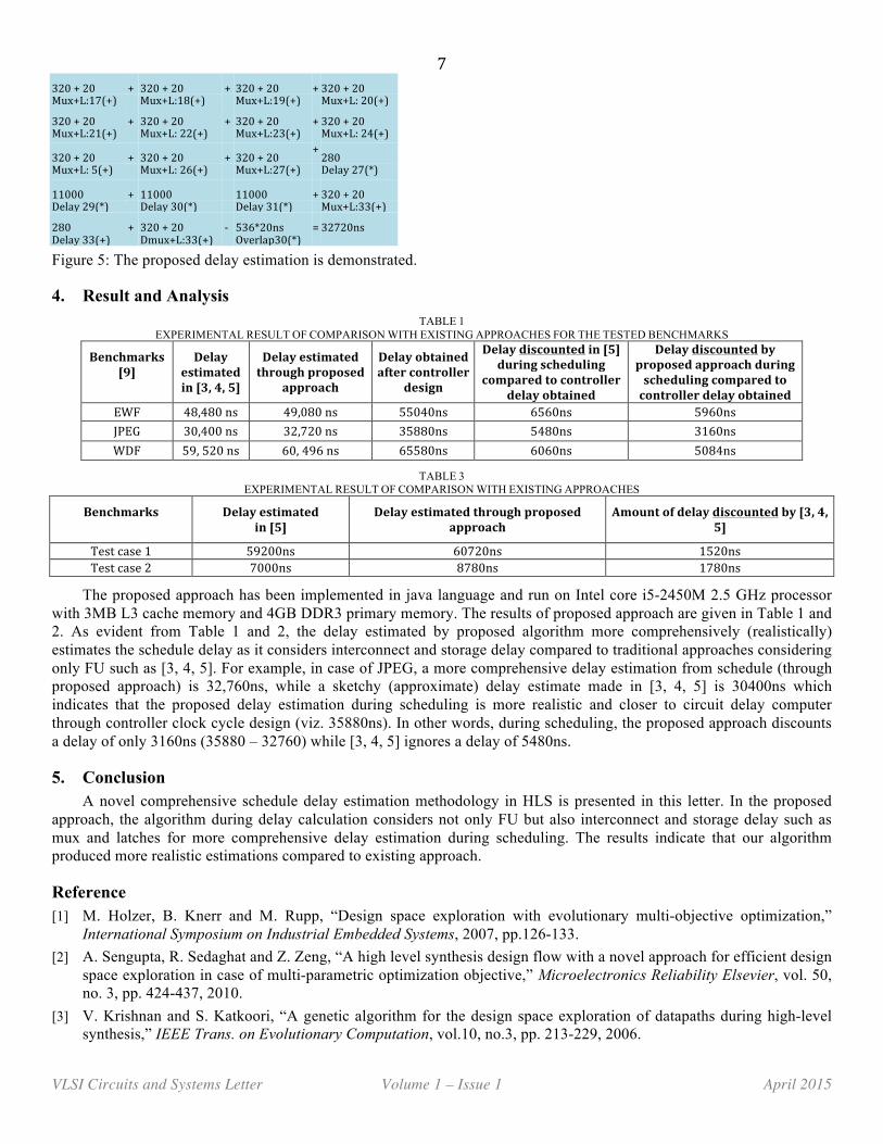
TABLE 3 EXPERIMENTAL RESULT OF COMPARISON WITH EXISTING APPROACHES
Benchmarks
Delay estimated in [5]
Delay estimated through proposed approach
Amount of delay discounted by [3, 4, 5]
Test case 1 59200ns 60720ns 1520ns Test case 2 7000ns 8780ns 1780ns
The proposed approach has been implemented in java language and run on Intel core i5-2450M 2.5 GHz processor with 3MB L3 cache memory and 4GB DDR3 primary memory. The results of proposed approach are given in Table 1 and 2. As evident from Table 1 and 2, the delay estimated by proposed algorithm more comprehensively (realistically) estimates the schedule delay as it considers interconnect and storage delay compared to traditional approaches considering only FU such as [3, 4, 5]. For example, in case of JPEG, a more comprehensive delay estimation from schedule (through proposed approach) is 32,760ns, while a sketchy (approximate) delay estimate made in [3, 4, 5] is 30400ns which indicates that the proposed delay estimation during scheduling is more realistic and closer to circuit delay computer through controller clock cycle design (viz. 35880ns). In other words, during scheduling, the proposed approach discounts a delay of only 3160ns (35880 – 32760) while [3, 4, 5] ignores a delay of 5480ns.
5. Conclusion A novel comprehensive schedule delay estimation methodology in HLS is presented in this letter. In the proposed
approach, the algorithm during delay calculation considers not only FU but also interconnect and storage delay such as mux and latches for more comprehensive delay estimation during scheduling. The results indicate that our algorithm produced more realistic estimations compared to existing approach.
Reference [1] M. Holzer, B. Knerr and M. Rupp, “Design space exploration with evolutionary multi-objective optimization,”
International Symposium on Industrial Embedded Systems, 2007, pp.126-133. [2] A. Sengupta, R. Sedaghat and Z. Zeng, “A high level synthesis design flow with a novel approach for efficient design
space exploration in case of multi-parametric optimization objective,” Microelectronics Reliability Elsevier, vol. 50, no. 3, pp. 424-437, 2010.
[3] V. Krishnan and S. Katkoori, “A genetic algorithm for the design space exploration of datapaths during high-level synthesis,” IEEE Trans. on Evolutionary Computation, vol.10, no.3, pp. 213-229, 2006.
8
VLSI Circuits and Systems Letter Volume 1 – Issue 1 April 2015
[4] V. Heijlingers, L. Cluitmans and J. Jess, “High-level synthesis scheduling and allocation using genetic algorithms”, Asia South Pacific Design Automation Conference, pp.61-66, 1995.
[5] A. Sengupta, R. Sedaghat and P. Sarkar, “A multi structure genetic algorithm for integrated design space exploration of scheduling and allocation in high level synthesis for DSP kernels,” Swarm and Evolutionary Computation, pp. 35-46, 2012.
[6] R. Harish., M. Bhuvaneswari and S. Prabhu, “A novel framework for applying multiobjective GA and PSO based approaches for simultaneous area, delay, and power optimization in high level synthesis of datapaths,” VLSI Design, Article ID 273276, 2012.
[7] A. Sllame, “Design space exploration methodology for high-performance system-on-a-chip hardware cores,” IEEE International Workshop on System-on-Chip for Real-Time Applications, pp. 216-221, 2003.
[8] G. Shanghua, et al., “Interconnect-aware pipeline synthesis for array-based architectures,” IEICE Trans. on Fundamentals of Electronics, Communications and Computer Sciences, vol. 92, no. 6, pp. 1464-1475, 2009.
[9] S. Mohanty, N. Ranganathan, E. Kougianos and P. Patra, Low-Power High-Level Synthesis for Nanoscale CMOS Circuits, Springer, 2008.
Standard Cell Pin Access Planning and Regular Routing for Self-Aligned Double Patterning David Z. Pan Department of Electrical and Computer Engineering, University of Texas at Austin, Austin, TX, US
Abstract – Pin access has become one of the most difficult challenges for detailed routing in 14nm technology node and beyond, where double patterning lithography has to be used for manufacturing lower metal layers with tight pitches. Self-aligned double patterning (SADP) provides better control on the line edge roughness and overlay but it has very restrictive design constraints and prefers regular layout patterns. This work presents a comprehensive pin access planning and regular routing framework (PARR) for SADP friendliness. The key techniques include pre-computation of both intra-cell and inter-cell pin accessibility, as well as local and global pin access planning to enable the handshaking between standard cell level pin access and detailed routing under the SADP constraints. Our experimental results demonstrate that PARR can achieve substantially improved routability and overlay control compared to the previous approaches.
1. Problem and Motivation In advanced technology nodes, standard cell (SC) input/output (I/O) pin access has become one of the most
challenging issues during physical design. For 14nm technology and beyond, self-aligned double patterning (SADP) is expected to be used for the lower metal layers with tight pitches. In spite of better control on overlay and line edge roughness, SADP prefers regular layout patterns and imposes a new set of layout constraints. Pin access has become much more difficult under these restrictions. Meanwhile, the density and area scaling for each technology node requires standard cells be compacted into a limited number of routing tracks, i.e., the fixed standard cell height. The access points of each I/O pin are thus limited and they interfere with each other under complex DFM rules.
The pin access problem is directly related to both standard cell design and detailed routing scheme. The access point selection and the routing order of nets play an important role in the ultimate pin accessibility or routability. A typical example is shown in Figure 1. The routed M2 wires in Figure 1(a) block the I/O pin of Cell 1 and the remaining net is not routable. In Figure 1(b), different access points are selected for net A and the failed net in Figure 1(a) is routed first, which leads to the successful routing of all the nets.
9
VLSI Circuits and Systems Letter Volume 1 – Issue 1 April 2015
Figure 1: Pin access for routing: (a) one net failure, and (b) success.
2. Proposed Solution
Figure 2: Single row PAG: (a) a row of cells with pre-routed M2 wires, and (b) PAG with blocked intra-cell pin access.
To systematically deal with the pin access issue, we propose a holistic pin-access planning and regular routing (PARR) framework, which consists of two stages: SC level pin accessibility prediction and detailed routing level pin access planning. At the SC level, intra-cell as well as inter-cell pin accessibility is pre-computed and stored. The intra-cell pin access computation yields a 2-D set of M2 wires for all valid hit-point combinations of each cell within the library. To quantify the pin access interference when cells are placed next to each other, inter-cell pin accessibility information is also computed and stored in a look-up table (LUT). Line-end extension and optimization are performed to ensure the SADP compliance. The LUT is constructed only on critical pin-access cells.
Our pin access planning strategies involve both local access point selection for the single-net routing and global net deferring during the sequential routing for multiple nets. The local access point selection scheme builds on the dynamic access point scoring from the intra-cell pin accessibility prediction. To efficiently enable net deferring, the single row pin access graph (PAG) is constructed for each row of placed cells, e.g. as shown in Figure 2. A path from the virtual source (s) to target (t) denotes the pin accessibility of the associated cells. We dynamically maintain the source-to-target path existence of each component of the PAG and compute the routing order. The PARR algorithms have been used to guide SADP-aware regular (1D) routing. Our experimental results have shown much better pin accessibility and SADP-friendliness compared to a state-of-the-art academic SADP-aware 2D router.
3. Future Work As this work is the first effort, to our best knowledge, to systematically enable the handshaking between standard cell
level and routing level pin access planning and co-optimization with consideration of SADP, we expect a lot of future research can be done, e.g., better standard cell I/O pin design itself, consideration of other multiple patterning and critical layer constraints, and monolithic 3D-IC pin access.
10
VLSI Circuits and Systems Letter Volume 1 – Issue 1 April 2015
Reference [1] X. Xu, B. Yu, J.-R. Gao, C.-L. Hsu and D. Z. Pan, “PARR: pin access planning and regular routing for self-aligned
double patterning,” Design Automation Conference, 2015 [2] X. Xu, B. Cline, G. Yeric, B. Yu and D. Z. Pan, “Self-aligned double patterning aware pin access and standard cell
layout co-optimization,” International Symposium on Physical Design, pp. 101-108, 2014.
11
VLSI Circuits and Systems Letter Volume 1 – Issue 1 April 2015
Opinions
Hardware Security: Past, Current, and Future Yier Jin Department of Electrical Engineering and Computer Science, University of Central Florida, Orlando, FL, USA
1. Hardware Security – Origination While research in security and its implementation in hardware has been ongoing for many decades, the concept of
hardware security was not formally introduced until the emergence of hardware Trojans and their detection methods. At its early stage, hardware security was solely referred to hardware Trojan designs, categorization, detection, and isolation.
Unlike software virus and software Trojans, hardware Trojans cannot be easily eliminated through firmware updating and therefore, are more harmful to computer systems. Hardware Trojans are designed by attackers to add unwanted functionality to the design and there is no standard procedure to design hardware Trojans, as its design is reliant upon the attackers goals and available resources. Despite this, hardware security researchers have categorized different Trojans. For example, authors in [1] divided Trojans into implicit payload and explicit payload based on the Trojan activities when triggered. A more detailed Trojan taxonomy can be found in [2], [3]. Various Trojan designs were also proposed based on the stealth of hardware Trojans and the impact they may cause [4]–[7]. While most of these Trojans are inserted at the RT-level, Trojan insertion is also possible through dopant manipulation [8].
As existing testing methods fall short in detecting malicious logic, dedicated hardware Trojan detection methods and trusted integrated circuit design have been developed in recent years [9]. A large body of hardware Trojan detection and prevention methods have been proposed, which can be divided into four main categories: (i) enhanced functional testing [10], (ii) side-channel fingerprinting [11], (iii) Trojan prevention and (iv) circuit hardening [12].
Enhanced functional testing method is based on the idea that hardware Trojans often rely on rarely triggered events. Therefore, researchers propose to either include those rare events in the testing patterns to trigger the Trojan during the testing stage [13], or analyze all rare events at the gate-level netlists to identify suspicious nodes which may serve as triggers [14]. This method suffers from the limitation that no standard definition for rare events exists, leaving a huge gap between standard testing patterns and rare event patterns.
Side-channel fingerprinting is another popular solution. Even though a hardware Trojan cannot be triggered easily during the testing stage and, thus, can evade functional testing, the inserted Trojan has to alter the parametric profile of a contaminated circuit [2], [15], [16]. The effectiveness of this method relies on the capability to differentiate side-channel signals of Trojan-infected circuits from Trojan-free circuits. Thus, advanced data analysis methods are utilized to help generate side-channel fingerprints by eliminating the increasing process variation and measurement noise [11], [17]. Various side-channel parameters and their combinations are chosen for fingerprint generation and Trojan detection, which include global power traces [11], local power traces [18], [19], path delays [1], [20], etc. Side-channel fingerprinting-based Trojan detection has been widely used for its non-intrusive property, but this method is developed based on the assumption that a golden model should be available for comparison, which is not often possible.
Trojan prevention and circuit hardening techniques try to modify the circuit’s structure with extra logic either to eliminate rare/suspicious events [12], [21], or to make the target circuit more sensitive to malicious modifications [22]. These methods are often combined with other Trojan detection methods to increase the detection accuracy or to lower testing cost. Even though circuit co-design techniques are used to lower the impact of additional logic in the target design, the extra protection logic will still impact circuit performance. Furthermore, the hardening structure can itself be target of hardware Trojans [23].
2. Hardware Security – Current Research For most of existing Trojan detection methods, scalability becomes a concern. Therefore, researchers started to look
into post-deployment methods leveraging post-deployment side-channel fingerprinting and on-chip equivalence checking. The key idea here was that stealthy hardware Trojans may easily evade detection methods during testing stage but, if triggered, they will cause large impact to side-channel fingerprinting or to circuit functionality.
12
VLSI Circuits and Systems Letter Volume 1 – Issue 1 April 2015
Towards this direction, a post-deployment trust evaluation structure is proposed [24]. But this trusted evaluation process has the limitation that it will only be triggered externally through primary inputs halting the normal operation and leaving plenty of time for attackers to trigger and mute the Trojans during the testing intervals. To overcome the shortage of this method, a real-time trust evaluation structure is proposed that can constantly monitor the operational status of the target circuit and report circuit abnormalities instantly [25]. Concurrent on-chip parity checking leveraging on resistive RAM is also developed for run-time hardware Trojan detection [26].
Besides hardware Trojan detection and prevention, the cur- rent research in hardware security domain is further expanded from fabricated chips to pre-silicon designs, mostly relying on formal methods where proof-carrying hardware (PCH) is a leading example. Proof-carrying hardware (PCH) is a newly proposed methodology to prevent malicious code insertion in third-party IP modules [27]. Following the PCH framework, IP consumers provide IP vendors with the functional specification and a set of security properties. Besides the register transfer (RT) level code, IP vendors will also prepare a proof to verify that the delivered IP core meets all security properties. Upon receiving the IP cores, IP users will validate the proof of security property by providing the code and the property proof to an automatic proof checker. This method has proved successful in protecting cryptographic circuits [28], [29] to microprocessors [30] hardware IP cores. Even though the PCH framework provides high level protection and adds trivial workload on IP consumers, it adds computational burden on IP providers, which increases IP development cost. Therefore, the PCH framework is currently suitable for military chips and chips in critical infrastructure where security is of highest priority.
Realizing the severity of counterfeit chips in critical systems, hardware security researchers started investigating into this area, hoping to detect faked or illegally marked chips before their deployment. Data analysis and machine learning methods have been used for recovered chip identification [31], [32]. On-chip aging sensor is another popular solution for counterfeit chip isolation [33]. Another emerging problem is IC overproduction and IP piracy [34]–[37], which occurs primarily because of lack of oversight and/or direct involvement in fabrication after passing the design over to the foundry. Effectively, there is no feasible solution to determine if the foundry is producing exactly what the consumer ordered, or if they have over-produced the chips. To solve this problem the idea of split manufacturing was proposed [38], [39], which enabled IP vendors to rely on overseas manufacturing services and not send the entire design information. In this method, front-end of the line (FEOL) which requires advanced technology is fabricated overseas but the back-end of the line (BEOL) is added in domestic foundries such that the overseas foundries only learn partial design data. However, the effectiveness of this method is still under discussion [40], [41].
Orthogonal to these hardware security areas is the development of security primitives, which is investigated due to its high efficiency and low cost compared to software solutions. The leading example is the physically unclonable function (PUF) which leverages process variations to generate unique identities for each chip [42]. The main criterion in PUF design is to include randomness, uniqueness, and enhance security. A large amount of work has been proposed recently to improve these metrics using error correction algorithms [43] and non- MOSFET technologies [44], [45].
3. Hardware Security – The Future While existing hardware security methods are mostly in the areas of chip manufacturing, circuit designing, and
circuit testing, the future trends will cover broader area to grant hardware active roles in system level protection. Specifically, two hardware security research areas will be introduced to show that hardware security from single layer to cross layers.
Researchers in emerging devices are currently investigating their applications in broader security areas. Due to the availability of large number of emerging device models such as graphene transistors, atomic switches, memristors, MOTT FET, spin FET, nanomagnetic and all-spin logic, spin wave devices, OST-RAM, magnetoresistive random-access memory (MRAM), spintronic devices, etc. [46], two fundamental questions have recently been raised related to their applications in the hardware security domain: 1) Can emerging technology provide a more efficient hardware infrastructure than CMOS technology in countering hardware Trojans and IP piracy? 2) What properties should the emerging technology - based hardware infrastructure provide so that software level protection schemes can be better supported? Most work in emerging technologies for security purposes to date has been in Physical Unclonable Functions (PUFs) [45] and crypto- graphic primitives. However, PUFs essentially leverage device-to-device process variation. In some sense this suggests that noisier devices are more useful. Orthogonal to these efforts, researchers try to leverage the unique properties of emerging technologies, other than relying on noisy devices, for IP protection and hardware attack prevention [47].
Another challenge stems from treating security as an afterthought, or something to only be addressed as problems are encountered. Currently, hardware level security policies are not enforced. Instead, hardware design focuses on
13
VLSI Circuits and Systems Letter Volume 1 – Issue 1 April 2015
functionality and performance. That is, the job of the underlying hardware processor is to simply implement the ISA effectively and consistently, offering performance improvements where possible, and keeping costs to a minimum. This is most likely due to the difficulty of specifying attack models accurately enough to cover all possible corner cases and the ease with which security solutions can be applied at the software level. Hardware security for software-level protection is more complex and time consuming to implement, and is potentially unprofitable if the secure hardware is easily circumventable. However, literature has recently been published demonstrating that, through hardware-supported solutions, the system can more efficiently protect itself from advanced software attacks such as return oriented programming [48] and malicious kernel extensions [49], [50]. More work towards this direction is expected in the future.
4. Conclusion We summarized the evolution process of hardware security and the past, the current and the emerging research topics
in this area. This summary provides a reference of hardware security research and, hopefully, would be a clear guide for researchers to join this area and push the boundary further.
Acknowledgement This work was supported in part by the National Science Foundation grant (CNS-1319105).
Reference [1] Y. Jin and Y. Makris, “Hardware Trojan detection using path delay fingerprint,” International Workshop on
Hardware-Oriented Security and Trust, pp. 51-57, 2008. [2] M. Tehranipoor and F. Koushanfar, “A survey of hardware Trojan taxonomy and detection,” Design Test of
Computers, vol. 27, pp. 10-25, 2010. [3] https://www.trust-hub.org/. [4] S. King, J. Tucek, A. Cozzie, C. Grier, W. Jiang and Y. Zhou, “Designing and implementing malicious hardware,”
USENIX Workshop on Large-Scale Exploits and Emergent Threats, pp. 1-8, 2008. [5] Y. Jin, N. Kupp and Y. Makris, “Experiences in hardware Trojan design and implementation,” International
Workshop on Hardware-Oriented Security and Trust, pp. 50-57, 2009. [6] Sturton, M. Hicks, D. Wagner and S. King, “Defeating UCI: Building stealthy and malicious hardware,” Symposium
on Security and Privacy, pp. 64-77, 2011. [7] J. Zhang and Q. Xu, “On hardware Trojan design and implementation at register-transfer level,” International
Symposium on Hardware-Oriented Security and Trust, pp. 107-112, 2013. [8] G. Becker, F. Regazzoni, C. Paar and W. Burleson, “Stealthy dopant-level hardware Trojans,” Cryptographic
Hardware and Embedded Systems, pp. 197-214. 2013. [9] R. Karri, J. Rajendran, K. Rosenfeld and M. Tehranipoor, “Trustworthy hardware: Identifying and classifying
hardware Trojans,” IEEE Computer, vol. 43, no. 10, pp. 39-46, 2010. [10] J. Rajendran, V. Jyothi and R. Karri, “Blue team red team approach to hardware trust assessment,” International
Conference on Computer Design, pp. 285-288, 2011. [11] Agrawal, S. Baktir, D. Karakoyunlu, P. Rohatgi and B. Sunar, “Trojan detection using IC fingerprinting,” Symposium
on Security and Privacy, pp. 296-310, 2007. [12] H. Salmani, M. Tehranipoor and J. Plusquellic, “New design strategy for improving hardware Trojan detection and
reducing Trojan activation time,” International Workshop on Hardware-Oriented Security and Trust, pp. 66-73, 2009.
[13] Wolff, C. Papachristou, S. Bhunia and R. Chakraborty, “Towards Trojan-free trusted ICs: problem analysis and detection scheme,” Design Automation and Test in Europe, pp. 1362-1365, 2008.
[14] A. Waksman, M. Suozzo and S. Sethumadhavan, “FANCI: identification of stealthy malicious logic using boolean functional analysis,” ACM SIGSAC Conference on Computer and Communications Security, pp. 697-708, 2013.
[15] Y. Jin and Y. Makris, “Hardware Trojans in wireless crypto-graphic ICs,” IEEE Design and Test of Computers, vol. 27, pp. 26-35, 2010.
[16] M. Li, A. Davoodi and M. Tehranipoor, “A sensor-assisted self-authentication framework for hardware Trojan detection,” Design, Automation Test in Europe Conference Exhibition, pp. 1331-1336, 2012.
[17] R. Chakraborty, F. Wolff, S. Paul, C. Papachristou and S. Bhunia, “MERO: a statistical approach for hardware Trojan detection,” Cryptographic Hardware and Embedded Systems, pp. 396-410, 2009.
14
VLSI Circuits and Systems Letter Volume 1 – Issue 1 April 2015
[18] R. Rad, X. Wang M. Tehranipoor and J. Plusquellic, “Power supply signal calibration techniques for improving detection resolution to hardware Trojans,” International Conference on Computer-Aided Design, pp. 632-639, 2008.
[19] R. Rad, J. Plusquellic and M. Tehranipoor, “Sensitivity analysis to hardware Trojans using power supply transient signals,” International Workshop on Hardware-Oriented Security and Trust, pp. 3-7, 2008.
[20] C. Lamech, R. Rad, M. Tehranipoor and J. Plusquellic, “An experimental analysis of power and delay signal-to-noise requirements for detecting Trojans and methods for achieving the required detection sensitivities,” IEEE Trans. on Information Forensics and Security, vol. 6, no. 3, pp. 1170- 1179, 2011.
[21] M. Hicks, M. Finnicum, S. T. King, M. M. K. Martin, and J. M. Smith, “Overcoming an untrusted computing base: Detecting and removing malicious hardware automatically,” Symposium on Security and Privacy, pp. 159-172, 2010.
[22] Y. Jin, N. Kupp and M. Makris, “DFTT: design for Trojan test,” International Conference on Electronics Circuits and Systems, pp. 1175-1178, 2010.
[23] Y. Jin and Y. Makris, “Is single Trojan detection scheme enough?,” International Conference on Computer Design, pp. 305-308, 2011.
[24] Y. Jin, D. Maliuk and Y Makris, “Post-deployment trust evaluation in wireless cryptographic ICs,” Design, Automation Test in Europe Conference Exhibition, pp. 965-970, 2012.
[25] Y. Jin and D. Sullivan, “Real-time trust evaluation in integrated circuits,” Design, Automation and Test in Europe Conference and Exhibition, pp. 1-6, 2014.
[26] Y. Liauw, Z. Zhang, W. Kim, A. Gamal, and S. Wong, “Nonvolatile 3d-fpga with monolithically stacked RRAM-based configuration memory,” International Solid-State Circuits Conference, pp. 406-408, 2012.
[27] Love, Y. Jin and Y. Makris, “Proof-carrying hardware intellectual property: A pathway to trusted module acquisition,” IEEE Trans. on Information Forensics and Security, vol. 7, no. 1, pp. 25-40, 2012.
[28] Y. Jin and Y. Makris, “Proof carrying-based information flow tracking for data secrecy protection and hardware trust,” VLSI Test Symposium, pp. 252-257, 2012.
[29] Y. Jin, B. Yang and Y. Makris, “Cycle-accurate information assurance by proof-carrying based signal sensitivity tracing,” International Symposium on Hardware-Oriented Security and Trust, pp. 99-106, 2013.
[30] Y. Jin and Y. Makris, “A proof-carrying based frame- work for trusted microprocessor IP,” International Conference on Computer-Aided Design, pp. 824-829, 2013.
[31] K. Huang, J. Carulli and Y. Makris, “Parametric counterfeit ic detection via support vector machines,” International Symposium on Defect and Fault Tolerance in VLSI and Nanotechnology Systems, pp. 7-12, 2012.
[32] X. Zhang, K. Xiao and M. Tehranipoor, “Path-delay fingerprinting for identification of recovered ICs,” International Symposium on Defect and Fault Tolerance in VLSI and Nanotechnology Systems, pp. 13-18, 2012.
[33] X. Wang, L. Winemberg, D. Su, D. Tran, S. George, S. Palosh, N. Amed, A. Dobin and M. Tehranipoor, “Aging adaption in integrated circuits using a novel built-in sensor,” IEEE Trans. on Computer-Aided Design of Integrated Circuits and Systems, , vol. 34, no. 1, pp. 109-121, 2015.
[34] J. Roy, F. Koushanfar and I. Markov, “Epic: ending piracy of integrated circuits,” Design, Automation and Test in Europe, pp. 1069-1074, 2008.
[35] J. Rajendran, Y. Pino, O. Sinanoglu and R. Karri, “Logic encryption: A fault analysis perspective,” Design, Automation and Test in Europe, pp. 953-958, 2012.
[36] J. Rajendran, H. Zhang, C. Zhang, G. Rose, Y. Pino, O. Sinanoglu and R. Karri, “Fault analysis-based logic encryption,” IEEE Trans. on Computers, vol. PP, no. 99, 2013.
[37] S. Dupuis, P. Ba, G. Natale, M. Flottes and B. Rouzeyre, “A novel hardware logic encryption technique for thwarting illegal overproduction and hardware Trojans,” International On-Line Testing Symposium, pp. 49-54, 2014.
[38] Imeson, A. Emtenan, S. Garg and M. Tripunitara, “Securing computer hardware using 3d integrated circuit (IC) technology and split manufacturing for obfuscation,” USENIX Security Symposium, pp. 495-510, 2013.
[39] K. Vaidyanathan, B. Das and L. Pileggi, “Detecting reliability attacks during split fabrication using test-only BEOL stack,” Design Automation Conference, 2014.
[40] J. Rajendran, O. Sinanoglu and R. Karri, “Is split manufacturing secure?,” Design, Automation Test in Europe Conference Exhibition, pp. 1259-1264, 2013.
[41] M. Jagasivamani, P. Gadfort, M. Sika, M. Bajura and M. Fritze, “Split-fabrication obfuscation: metrics and techniques,” International Symposium on Hardware-Oriented Security and Trust, pp. 7-12, 2014.
[42] Suh and S. Devadas, “Physical unclonable functions for device authentication and secret key generation,” Design Automation Conference, pp. 9-14, 2007.
[43] M. Hofer and C. Boehm, “An alternative to error correction for SRAM-like PUFs,” Cryptographic Hardware and Embedded Systems, pp. 335-350. 2010.
15
VLSI Circuits and Systems Letter Volume 1 – Issue 1 April 2015
[44] W. Che, J. Plusquellic and S. Bhunia, “A non-volatile memory based physically unclonable function without helper data,” International Conference on Computer-Aided Design, pp. 148-153, 2014.
[45] A. Iyengar, K. Ramclam and S. Ghosh, “DWM-PUF: a low- overhead, memory-based security primitive,” International Symposium on Hardware-Oriented Security and Trust, pp. 154-159, 2014.
[46] International Technology Roadmap for Semiconductor (ITRS), http://www.itrs.net/. [47] Y. Bi, P. Gaillardon, X. Hu, M. Niemier, J. Yuan and Y. Jin, “Leveraging emerging technology for hardware security
- case study on silicon nanowire FETs and graphene SymFETs,” Asian Test Symposium, pp. 342-347, 2014. [48] L. Davi, P. Koeberl and A. Sadeghi, “Hardware-assisted fine-grained control-flow integrity: towards efficient
protection of embedded systems against software exploitation,” Design Automation Conference, 2014. [49] Y. Jin and D. Oliveira, “Trustworthy SOC architecture with on-demand security policies and HW-SW cooperation,”
Workshop on SoCs, Heterogeneous Architectures and Workloads, 2014. [50] D. Oliveira, J. Navarro, N. Wetzel, and M. Bucci, “Ianus: Secure and holistic coexistence with kernel ex tensions - an
immune system-inspired approach,” ACM Symposium on Applied Computing, pp. 1672-1679, 2014.
Intelligent Embedded Systems: Trends and Opportunities Theocharis Theocharides Department of Electrical and Computer Engineering, University of Cyprus, Nicosia, Cyprus
Smart networked embedded systems (or cyber-physical systems (CPS)) can be described as smart systems that encompass computational (i.e., hardware and software) and physical components, seamlessly integrated and closely interacting to sense the changing state of the real world (i.e. humans, environment, etc.). These systems involve a high degree of complexity at numerous spatial and temporal scales and highly networked communications integrating computational and physical components. These new technologies are enabling a new generation of ‘smart systems’ – and the economic impacts are enormous [1]. The disruptive technologies emerging from combining the cyber and physical worlds could provide an innovation engine for a broad range of industries, creating entirely new markets and platforms for growth. New products and services will bring the creation and retention of jobs, and the world will also benefit through greater energy and security, enhanced industrial competitiveness, and improved quality of life for citizens. In particular, cyber-physical systems (CPS) are characterized by a diverse group of systems used to physically manipulate critical infrastructure, such as power, water and oil/natural gas pipelines, industrial systems, transportation systems, medical devices, security systems, building automation, emergency management, and many other systems vital to our well-being. When these systems malfunction or fail, the operation of corresponding systems in the real world can impair physical safety or trigger loss of life, cause enormous economic damage, and thwart the vital missions of businesses, cities, and even entire nations. Typical systems are designed to meet the following criteria: process large amount of data; employ (mostly) hardware and software as a system components; run online continuously; and possibly maintain an operator-in-the-loop because of human judgment and accountability requirements for safety-critical systems. Systems that meet these criteria include among others energy systems, automotive and transportation systems, biomedical systems, and many more. These systems do not operate in a controlled environment, and must be robust to unexpected conditions and adaptable to subsystem failures. It is often not possible to perform robust testing of these systems prior to actual deployment because the physical devices are so expensive that they cannot be replicated in the testing lab, or at least not for large-scale operation.
16
VLSI Circuits and Systems Letter Volume 1 – Issue 1 April 2015
Figure 1: Towards intelligent embedded systems: from sensors to sense.
Over the last few years in particular, cyber-physical systems feature high-bandwidth wired and wireless communication, and sensors such as extremely sensitive but accurate gyroscopes, high-resolution cameras and microphones, and other sensors that can virtually emulate the way humans sense their environment. The sensor technology being developed allows computing devices to flawlessly receive context information much like humans use their five senses: touch interfaces, smart cameras featuring vision capabilities such as detection and recognition, microphones and speech recognition are already present in many devices [4]. Furthermore, chemical sensors, which when coming in contact with various substances react and produce certain current levels which can then be associated with the substance, let that be gas or liquid, can be used to enable systems to smell and taste! These ground breaking sensing technologies, already integrated in modern embedded systems, provide them with all the information necessary to help them become aware of their context. A very simple, yet highly efficient example involves Samsung’s SmartScrollTM
technology integrated into its mobile devices, where an eye-tracking sensor recognizes when the user looks at the screen, and engages automatic text scrolling responding to the user’s viewpoint to ease the user’s reading effort. Similarly, the eye sensor can be used to raise or lower the LCD’s brightness, turning it up whenever the user is looking at the screen, or lowering it whenever the user looks elsewhere. While the first example seemingly appears as a gimmick, the second one has significant impact on power savings, prolonging battery life.
As the amount of data processed by the system (sensors to processing nodes) increases drastically, traditional approaches and algorithms used for context-awareness are required to elevate their performance over a much larger and broader spectrum of information understanding, with the complexity rising exponentially. Overall, software-based context-awareness algorithms have been used successfully in such scenarios, with their performance being satisfactory so far; such software, running on general-purpose microprocessors that modern embedded computing systems are equipped, can perform relatively close to real-time context recognition and have been used extensively on embedded systems so far. However, with the emergence of improved and novel sensing technologies, and the targeted portability of such systems, and with the associated implications in low energy consumption and extreme thermal constraints, software-based solutions are not adequate anymore. Software-based algorithms require high-end general processors to provide marginal real-time performance and continue provide context awareness to emerging embedded devices. Moreover, software implementations of data mining, data fusion and pattern recognition algorithms (that enable the system to gather data, process it in real-time and decide what action to take next) demand high processing capabilities, and thus require high-end general-purpose processors. Thus, over the latest years, special-purpose, custom VLSI architectures have been proposed to accelerate these algorithms, and the initial research outcomes are more than promising: special purpose hardware can accelerate computer vision applications, which traditionally feature such complicated algorithms used in context awareness, achieving real-time performance with minor compensations in accuracy [5-8].
At the same time, research in reconfigurable hardware systems is yielding encouraging results; partial and dynamic reconfiguration of the hardware fabric while the host system is running is gradually used in a wide range of reconfigurable applications and is also available in commercial state-of-the-art Field-Programmable Gate Arrays (FPGAs). Programmable on-chip interconnects have also been proposed for multi-core CPUs. Partial reconfiguration currently is strongly application-driven, and ongoing research investigates issues such as granularity, tools, runtime software issues,
17
VLSI Circuits and Systems Letter Volume 1 – Issue 1 April 2015
etc. The initially-optimistic evolutionary and adaptive hardware vision proposed almost 20 years ago [3] is now feasible [8], as the on-going research is producing a large number of experimental prototypes. While evolutionary and adaptive hardware has been in the background for quite some time now, only recently we are seeing some applied results. Typically, reconfiguration is event-triggered, and the system is pre-configured with certain operational parameters that can be dynamically adjusted at run-time depending on the event that triggered the reconfiguration. Alternatively, the system learns to adapt on its own through information passed to it either through sensors, or the user. Evolvable hardware design integrates evolutionary algorithms that encapsulate reconfigurable hardware (aided by dynamic, partial reconfiguration facilitated in modern FPGAs), artificial intelligence and fault-tolerance, in an effort to aid a system to autonomously alter its system hardware architecture and behaviour dynamically to adapt and interact to its environment. Recent work proposes the use of Artificial Neural Networks as a predictive mechanism to forecast context changes (such as for predictive traffic hotspots or extremely low utilization of communication links within a network-connected chip multi-processor) within a system-on-chip and adjust the hardware operational parameters (such as turning off certain communication links, or switch to an adaptive flow-control algorithm that can prevent “bad” traffic hotspots from happening [7-8]. The obtained results are also encouraging and indicate that even a simple intelligent algorithm that can operate in real time (embedded within the system hardware), can potentially forecast the operational context in which a system might be entering, and enable the system to reconfigure its hardware to prevent certain bad scenarios from happening, or take advantage of potential good scenarios that might be arising. The opportunities stemming from these capabilities could be enormous; much like a human uses the five senses to learn and adapt to its environment, these systems could be designed to learn from their environment, reconfigure themselves and adapt (and possibly evolve) to address emerging changing states of their operation, and operate reliably, efficiently, and with the lowest energy consumption possible. As such, the vision of the late Mark Weiser [2] is now starting to become true.
Reference [1] “The future of enterprise computing: preparing for the compute continuum”, Intel White Paper, May 2011. [2] M. Weiser, “The computer for the twenty-first century”, Scientific American, vol. 265, no. 3, pp.94-104, 1991. [3] A. Thompson, “Hardware evolution: automatic design of electronic circuits in reconfigurable hardware by artificial
evolution”, Distinguished Dissertations, Springer, 1998. [4] M. Baldau, S. Dustdar and F. Rosenberg, “A survey on context-aware systems”, International Journal of Ad Hoc and
Ubiquitous Computing, vol. 2, no. 4, pp. 263-277, 2007. [5] Kyrkou and T. Theocharides, “A flexible parallel hardware architecture for AdaBoost-based real-time object
detection," IEEE Trans. on Very Large Scale Integration Systems, vol.19, no.6, pp.1034-1047, June 2011. [6] Kyrkou, and T. Theocharides, “A parallel hardware architecture for real-time object detection with support vector
machines,” IEEE Trans. on Computers, vol.61, no.6, pp.831-842, June 2012. [7] Kakoulli, V. Soteriou and T. Theocharides, “Intelligent hotspot prediction for network-on-chip-based multicore
systems,” IEEE Trans. on Computer-Aided Design of Integrated Circuits and Systems, vol.31, no.3, pp.418-431, March 2012.
[8] V. Soteriou, T. Theocharides and E. Kakoulli, “A holistic approach towards intelligent hotspot prevention in network-on-chip-based multicores”, IEEE Trans. on Computers, 2015.
Beyond Silicon: Is DNA Computer Going to be the Future? Prasun Ghosal and Mayukh Sarkar Indian Institute of Engineering Science and Technology, Shibpur, India
As chip designers are working relentlessly towards the development of newer high performance processors and / or other hardware components to cater the need of next generation computing, technologists are equally eager to find out newer materials and technologies to overcome the death threat towards the CMOS industry. With current growth in VLSI technology, the integration density of the transistors has reached billions, pushing the silicon technology towards its limits of transistor size, energy consumption etc. In reality, whatever be the pace and efficiency, we must have to face the wall very soon as per the ITRS (International Technology Roadmap for Semiconductors) prediction. Therefore, groups of researchers are continuously searching for an unconventional but perfect replacement of this technology / material in
18
VLSI Circuits and Systems Letter Volume 1 – Issue 1 April 2015
parallel to develop future generation computers. As a result, emergence of new computing technologies, viz. computing using the principles of quantum mechanics, or computing at molecular levels using DNA and RNA has introduced a new paradigm. Though in not so mature form, success of DNA Computing (also known as Bio-molecular Computing) in solving several very hard, computationally intensive problems have shown the way of perfect replacement of tomorrow’s high performance computing needs. Recent researches on DNA Computing to prove it’s applicability on conventional computing problems too with comparative performance have raised the question of whether this new technology can entirely replace the conventional silicon technology in fruitful way. Promising success in research on implementing the operations in a Bio-molecular laboratory has fortified the claim.
1. DNA Structure and Operations The DNA (Deoxyribonucleic acid), found in the living cells, is composed of four bases, viz. Adenine(A),
Guanine(G), Thiamine(T), and Cytosine(C). The order of these bases is unique in each individual, and determines the unique characteristics of that particular individual. Each base is attached to its neighboring base in the sequence via phosphate bonding. Two DNA sequences bond with each other via hydrogen bonding between each Watson-Crick complementary base pairs (A with T, and C with G), forming DNA double helix. Each DNA strand has two ends: 5’-end and 3’-end, that determine the polarity of the DNA strand. During the formation of DNA double strand, two complementary single strands bond with each other in anti-parallel fashion.
Following operations are possible to perform on DNA solution in a bio-molecular laboratory. • Anneal: On cooling up a solution, complementary DNA strands join with each other to form double strands. • Denature: When a solution is heated enough to break the hydrogen bonds between the complementary pairs forming
the double strands, the double strands break to form single strands. • Cut: Several restriction enzymes detect particular restriction sites of a DNA strand, and cut between them to form
two separate strands. • Separate by string: To separate DNA strands having particular string, magnetic bead with the corresponding
complementary strand is used to attract the desired strands. • Separate by length: Gel Electrophoresis method is used to separate the DNA strands by their length. • Ligase: Ligation enzyme is used to append one DNA strand with another.
2. Emergence of DNA Computing The introduction as well as success story of DNA Computing has started just a couple of decades back when in 1994,
Adleman [1] showed the way to solve computational problems using DNA molecules by solving the Hamiltonian Circuit Path problem (or Travelling Salesman Problem) in linear time, which is, otherwise, a computationally hard problem for conventional computers. The very next year, Lipton [2] solved the SAT problem, in a very similar manner as Adleman, by representing all possible combinations of values in a graph. Lipton’s DNA algorithm for solving the SAT problem was a linear one, which is impossible for a conventional computer at this stage. In the same year, Boneh et al. [3] broke DES using DNA. In 1997, Ouyang et. al. [4] solved the maximal clique problem given a six-vertex graph. Along with these experiments, several other NP-complete problems, e.g. Graph Coloring [5], Bin Packing [6] etc. have been solved using DNA computing.
3. Advantages of DNA Computer Primary reason behind the fact that the so-called computationally hard problems can be solved on a DNA computer
in reasonable time is manifold. Here are some of the salient points. • Information density: The information density of DNA is huge over silicon. Estimated storage capacity of 2.2 PB per
gram of DNA has been reported in [7]. • Massively parallel operation: A single gram of DNA solution can contain nearly 1018 DNA molecules of 2000bp,
and all operations performed on a solution of DNA molecules affect all the molecules at the same time. So, it may be considered as 1018 operations are performed in parallel in a DNA solution, i.e. 1018 processors work in parallel.
• Energy efficiency: Nearly 1019 operations can be performed per Joule that simply makes a DNA computer nearly billion times more energy efficient than a silicon computer.
4. Challenges and Promises
19
VLSI Circuits and Systems Letter Volume 1 – Issue 1 April 2015
DNA computer is already proven as a powerful technology for computationally hard problems that requires search over a huge search space. But one interesting point is the DNA algorithms does not simplify original algorithms but huge information density and massively parallel operations are what allows DNA computer to search over the huge search space in linear or polynomial time. For example, Adleman's original experiment would require huge amount of DNA with the increase of nodes in the graph. So, it is encouraged to find out a way to improve the algorithms over the conventional ones for DNA computer in parallel to solve more computationally hard problems.
DNA computer is proven to be better for computationally hard problem with brute-force search over huge search space. To make conventional silicon computer completely replaceable by the DNA computer other problems those are solvable on the conventional computer should also be made to be solvable on the DNA computer. A complete ALU unlike conventional computer is needed for the same. So, challenge lies in implementing arithmetic and logic operations using DNA molecules with similar DNA structure for input and output so that they are easy to implement and can be used in an automated DNA computer. Removing human intervention during the operation of a DNA computer is still a challenge.
Not only in solving computationally hard problems but DNA computing, since its inception, has seen several other areas to get applied. Most of them are still in their infancy e.g. DNA cryptography, and Steganography. During last few years this area has seen some real advancement and still needs to be explored. But even in its first stage it proved to be groundbreaking in the future of cryptography. For example, the simplest procedure to hide data using DNA using PCR with 20-mer primers at both ends (the data DNA strand is hidden in several other dummy DNA strands in a solution and the primers act as the keys to amplify and get the correct data DNA to the receiver) is proven to be powerful than 56-bit DES technology, because, brute-force search of two 20-mer primers needs the search space of 440 , whereas the search space of 56-bit DES is only 256. So, designing more powerful DNA Cryptography and Steganography techniques may be considered as another challenge as well as future promise from DNA computing.
Reference [1] L. Adleman, “Molecular computation of solutions to combinatorial problems,” Science, vol. 266, pp. 1021-1024,
Nov. 1994. [2] R. Lipton, “DNA solution of hard computational problems,” Science, vol. 268, pp. 542-545, Apr. 1995. [3] Boneh, C. Dunworth and R. Lipton, “Breaking DES using a molecular computer.” DIMACS workshop on DNA
computing, 1995. [4] Q. Ouyang, P. Kaplan, S. Liu and A. Libchaber, “DNA solution of the maximal clique problem.” Science, vol. 278,
pp. 446-449, Oct. 1997. [5] Y. Liu, J. Xu, L. Pan and S. Wang, “DNA solution of a graph coloring problem.” J Chem Inf Comput Sci., vol. 42,
pp. 524-528, May-Jun 2002. [6] Sanches and N. Y. Soma, “A polynomial-time DNA computing solution for the bin-packing problem,” Applied
Mathematics and Computation, vol. 215, pp. 2055-2062, 2009. [7] N. Goldman, P. Bertone, S. Chen, C. Dessimoz, E. LeProust, B. Sipos and E. Birney, “Towards practical, high-
capacity, low-maintenance information storage in synthesized DNA,” Nature, vol. 494, pp. 77-80, Feb. 2013.
New Frontiers in Wireless Network-on-Chip Designs Amlan Ganguly, Naseef Mansoor and Md Shahriar Shamim Rochester Institute of Technology, Rochester, NY, USA
20
VLSI Circuits and Systems Letter Volume 1 – Issue 1 April 2015
Figure 1: An architecture example is shown for wireless NoCs.
Modern and future multicore chips will integrate hundreds to thousands of computing elements on the same die. The designs will vary from homogeneous tile based architectures to heterogeneous integrations involving disparate technologies or differentiated processing modules. One common design challenge in all these otherwise architecturally different systems is the interconnection backbone for the large system. The rapidly scaling system sizes aggravates the problem by making traditional shared bus architectures obsolete. Scalable packet-switched Network-on-Chip provides a solution in which design complexity does not increase with size [1]. However, that causes, increase in latencies and energy consumption coupled with decrease in data throughput in such on-chip network environments. However, the timing and energy overheads in on-chip communication have to adhere to stringent budget constraints while achieving high reliability and nearly lossless packet transfer. Such conflicting goals are impossible to achieve with traditional metal/dielectric based interconnection systems in existence today. Consequently, emerging interconnect technologies like photonic, wireless and RF paradigms are envisioned to replace or augment existing systems. While these emerging technologies present new challenges they promise orders of magnitude improvements in latency and energy consumption in on-chip data communication if successfully adopted in multicore chips with several hundred processing elements. Wireless interconnects (WIs) [2] in particular bring an additional degree of freedom eliminating the need for physical interconnect layout potentially paving the way for reconfigurable low latency and energy efficient NoC topologies which will find use due to the scenarios discussed below: • Unbalanced workloads, thermal emergencies and dynamic task mappings: Multicore chips will experience
dynamically variable workloads depending on several factors. From uneven workload distribution to temperature-aware dynamic thread migrations due to thermal emergencies can result in uneven bandwidth and latency demands from the underlying NoC fabric. Heterogeneous multicore chips integrating CPUs, GPUs, FPGA fabrics and memories inherently have unequal bandwidth demands from the NoC. Moreover, all task threads may not benefit to the same extent from higher bandwidth. This implies that naively deploying excess bandwidth to all communication pairs on the chip will cause wasted resources and energy consumption. To minimize such wastage and maximize resource utilization, dynamic policies for distribution of the wireless bandwidth and interconnect resources need to be investigated. It is recognized that a distributed, asynchronous policy enabling multiple transceiver pairs to access and fairly share the wireless bandwidth depending on their instantaneous needs is necessary to maximize utilization and minimize wastage.
• Inter and Intra chip wireless communication: Inter-chip communication is limited by the speed and bandwidth of the inter-chip interconnections. Traditional high speed serial I/O modules suffer from low density due to high crosstalk and large form factors. Also, power hungry transceiver circuits are necessary for the required signal conditioning on such inter-chip interconnects. More recently optical inter-chip interconnections are being investigated. While such links have higher bandwidth their integration with CMOS chips remain a challenge. The issues of inter-channel crosstalk also plague photonic interconnects. Wireless interconnects can be used to seamlessly establish networked connections between communicating pairs both on-chip as well as across multiple chips. Nodes in different chips can communicate with direct low latency and low power wireless links. This eliminates the need for
21
VLSI Circuits and Systems Letter Volume 1 – Issue 1 April 2015
multi-hop data transfer from source to the peripheral I/O modules and switching between on-chip and off-chip protocols. Thus direct inter and intra-chip wireless networks can reduce communication latency and energy consumption significantly. New research establishing the benefits and feasibility of such inter and intra-chip wireless networks need to be undertaken. Inter-chip networks may span systems-in-packages to boards, racks and even full warehouse scale datacenters. The technology requirements for enabling such wireless data centers need to be established through thorough research.
Reference [1] L. Benini and G. Micheli, “Networks on chips: a new SoC paradigm,” IEEE Computer, vol. 35, no. 1, pp. 70-78,
January 2002. [2] A. Ganguly, K. Chang, S. Deb, P. Pande, B. Belzer and C. Teuscher, “Scalable hybrid wireless network-on-chip
architectures for multicore systems,” IEEE Trans. on Computers, vol. 60, no. 10, pp. 1485-1502, 2011.
Emerging Technologies at Post-CMOS Era Cheng Zhuo Intel Corporation, Portland, OR, USA
1. Overview In the past few decades, the semiconductor industry has been fighting to keep Moore’s Law alive by numer- ous
innovations in silicon-based complementary metal-oxide- semiconductor (CMOS) field-effect transistor (FET) [1]–[3]. The Moore’s Law predicts that, under a similar cost, the number of transistors placed on an integrated circuit (IC) chip would approximately double every two years. Such continuous scaling delivers economical products with higher computation efficiency, lower cost per function, and smaller dimension, as compared with their predecessors [1]–[3]. This is also the primary driver for the semiconductor industry to bring CMOS ICs to our daily life, ranging from wearable devices to high performance PCs.
However, with the technology node shrinking further down to below 14nm, the CMOS feature size is approaching the quantum physics boundaries. This prevents the Moore’s Law from continuing in its conventional way. Even if CMOS tran- sistor dimension could continue shrinking down, the benefits of scaling are disappearing and issues are arising: • Computation efficiency of conventional CMOS is limited by the subthreshold slope of 60 mV/dec at room tem-‐ perature
[2]–[4]. The supply voltage cannot be scaled as aggressively as before without increasing the leakage or reducing the drive current.
• More stringent power consumption constraints prohibit simultaneous turning on of all the transistors, thereby leaving more transistors remaining passive or idle [5].
• Increased electrical field inside the transistors may result in reliability issues and mobility degradations [2], [3]. • Last but not the least, variability and yield challenges render the cost per transistor prohibitively expensive.
In order to address all these issues and concerns, much research effort have been carried out to deliver long-term continued scaling with increasing computational performance and decreasing cost at post-CMOS era, ranging from material, device to architecture and system. In recent years, research on non-CMOS paradigms have proven to be a promising alternative to extending Moore’s Law [3], [6]–[9]. Unlike conventional CMOS, some of these novel devices do not operate under the principles of thermionic emission and use electron charge to store and transfer information. Thus, we are presented with new challenges and research opportunities to investigate these unusual responses from device, transportation to architecture and system for future high-performance com- puting. This paper will provide a brief overview and discuss both the favorable attributes and challenges of a few represen- tative emerging technologies at post-CMOS era, which can be further categorized into the following three topics: 1) Carbon nanotube based circuits; 2) Spin logic and memory; 3) TSV- inductor.
2. Carbon Nanotube Based Circuits Carbon nanotubes (CNT) are hollow, seamless, cylindrical nano-structures of carbon atoms [7], [10], [11].
Depending on how the sheets of carbon are rolled up during growth, its structure can possess different properties,
22
VLSI Circuits and Systems Letter Volume 1 – Issue 1 April 2015
semiconductor or metal. Thus, a single or an array of CNTs can be used as channel materials in a conventional MOSFET structure, which was first demonstrated in 1998 [13], [14]. Due to its small size and one dimension characteristic, compared with conven- tional MOSFET, CNTFET is found to have better Ion/Ioff ratio, higher transconductance, higher mobility, and higher integration density [6], [7], [15], [16]. Moreover, the metal and semiconductor properties in CNT indicate a possibility for a fully-CNT-based circuit design or even processor, with metal CNT for interconnect and semiconductor CNT for device.
Due to its promising material properties, many experts, from chemists to circuit designers, have been actively involved in its development. Various circuit architectures, ranging from simple logic gate, ring oscillator to decoder and sensor in- terface, have been built [17]–[22]. A CNT global router to facilitate the system design has been presented to integrate copper and CNT interconnect routing [23]. However, many fundamental problems still exist and are extremely difficult to address before CNTFET can be widely applied in commercial products [7], [20], [21], [24], [25]. A lot of effort are focused on isolation between semiconductor CNT and metal CNT, which have very similar diameters and physical structure, in order to achieve desired purity. On the device side, the device variation is a big concern (similar to conventional MOSFET) due to alignment, positioning and growth variabilities. In order to overcome some of the aforementioned issues, fault tolerant circuit architectures are proposed and studied, which comes at a cost of area, power and speed. Based on that, reference [26] proposes and implements the first full-CNT computer running a multitasking operation system. The processor uses 178 CNTFETs with each comprising 10-200 CNTs [26]. This milestone convincingly establishes CNTFET as one of the most promising candidates for future nanoelectronics, though there is still a long way to go for mass production with high yield and reasonable cost [6], [7].
3. Spin Logic and Memory Unlike electron based CNTFET discussed in the previous section, spintronics uses and controls the spin to represent
information in ferromagnetic thin films based devices [6], [8], [27]–[30]. Since the discovery of magnetic tunneling junction (MTJ), the spin based circuits including both memory and logic have been actively exploited [8], [27], [31], [32]. The two states (high and low resistance) of MTJ need to be controlled by either magnetic field or a spin polarized current to enable information storage and transfer. The proposal of spin transfer torque (STT) resolves the issue of large current demands for MTJ control and instead, only requires a small bidirectional current [33]–[37]. This not only reduces power consumption but also increases the integration density, thereby making spin based IC a promising alternative to CMOS [36], [37].
Spin-based logic and memory have many appealing and competitive features, including low power and cost, high integration density, good compatibility, as well as the added bonus of non-volatility [6], [8], [27], [28]. Many prototypes have been proposed and implemented in the past decade from both academia and industry, including magneto-resistive RAM (MRAM), hybrid MTJ/CMOS logic, all-spin logic, spin- FET and domain wall based logic/memory, etc. [29], [30], [39]–[47]. However, there are still many remaining challenges preventing its immediate application, e.g., reliability, clock control, gain circuitry and manufacturability [6], [8], [27]– [30]. Even with the maturity of devices, the architecture study falls behind [6], [8]. In other words, it is highly desired to realize new architectures, which take full advantage of these non-CMOS devices for non-volatile operation, low energy- delay products and satisfactory logical efficiency. A lack of comprehensive supporting tools for synthesis, analysis and physical design also prevents designers from further explor- ing spintronics for post-CMOS computing, where numerous research opportunities lie for the CAD and design community [48].
4. TSV Inductor 3D ICs are another promising alternative beyond Moore’s Law [9]. Instead of making transistors smaller, it utilizes
vertical dimension for higher integration density, shorter wire length, smaller footprint, higher speed, lower power consump- tion, and, more importantly, full compatibility with current technology. The through-silicon-via (TSV) is a critical en- abling element for 3D ICs, which forms vertical signal, power and thermal paths [49], [50]. A very large number of TSVs are inserted into the design to perform desired functions, and provide redundancy to ensure manufacturability [49], [50]. To alleviate the cost of redundancy, there have been effort in the literature to make use of those dummy TSVs for alternative purposes. One promising application is to use TSVs towards on-chip inductors, which are critical components in various microelectronic applications, e.g. on-chip voltage regulators, resonant clocking, voltage control oscillators, power amplifiers and radio frequency (RF) circuits, etc. [51]–[59].
Conventional implementation of on-chip inductors uses the multi-turn planar spiral structure. This structure occupies a significantly large area and may require special process for higher quality factor. For example, reference [60] reported
23
VLSI Circuits and Systems Letter Volume 1 – Issue 1 April 2015
an inductor occupying 78400 µm2, equivalent to the area of 62K gates in 45 nm technology. In 3D ICs, however, it is feasible to utilize TSVs to flip the inductor plane and build vertical inductors. This approach may save more than 70% area to achieve similar inductance compared to the spiral inductor [55], [56].
On the other hand, due to the substrate loss, the TSV- inductor loses its competitiveness at higher frequency range [55], [56]. Both the inductance and quality factor may start to degrade after giga or tens of giga Hz depending on the inductor dimension and structure. Thus, TSV-inductor is more favorable to low frequency applications, such as inductive DC-DC converters and LC resonant clocking. References [55] and [57] present applications of TSV-inductor in an on-chip regulator and global resonant clocking, and report 70-85% area saving without performance loss compared to the conventional spiral inductor design. In summary, TSV-inductor has proved to be a potential candidate for future on-chip inductor implementation for post-CMOS designs. However, more research effort are demanded on its AC loss, reliability and manufacturability.
5. Conclusion We discussed and summarized several emerging technolo- gies at post-CMOS era, including CNTFET, spin logic
and memory, and TSV-inductor. Each of these novel structures has its own potential to continue the future long-term scal- ing, but also confronts its own limitations from materials to manufacturability. This summary serves as a reference of these technologies and, hopefully, provides interesting and inspiring topics for researchers from circuit and CAD communities for the upcoming post-CMOS era.
Reference [1] S. Thompson and S. Parthasarathy, “Moore’s law: the future of Si microelectronics,” Elsevier Materials Today, vol.
9, no. 6, pp. 20-25, 2006. [2] M. Bohr, “A 30 year retrospective on Dennard’s MOSFET scaling paper,” IEEE Solid-State Circuits Society
Newsletter, vol. 12, no. 1, pp. 11-13, 2007. [3] M. Bohr, “The new era of scaling in an SoC world,” Available at: http://cseweb.ucsd.edu/classes/wi10/
cse241a/slides/Bohr.pdf. [4] K. Cheung, “On the 60 mV/dec @300 K limit for MOSFET subthreshold swing,” VLSI-TSA, pp. 72-73, 2010. [5] H. Esmaeilzadeh, et.al., “Dark silicon and the end of multicore scaling,” ISCA, pp. 365-376, 2011. [6] K. Bernstein, K. Cavin, A. Seabaugh and J. Welser, “Device and architecture outlook for beyond CMOS switches,”
Proceedings of The IEEE, vol. 98, no. 12, pp. 2169-2184, 2010. [7] J. Appenzeller, “Carbon nanotubes for high-performance electronics - progress and prospect,” Proceedings of The
IEEE, vol. 96, no. 2, pp. 201-211, 2008. [8] S. Sugahara and J. Nitta, “Spin-transistor electronics: an overview and outlook,” Proceedings of The IEEE, vol. 98,
no. 12, pp. 2124-2154, 2010. [9] P. Franzon, W. Davis and T. Thorolffson, “Creating 3D specific systems: architecture, design and CAD,” DATE, pp.
1684-1688, 2010. [10] P. Ajayan and T. Ebbesen, “Nanometre-size tubes of carbon,” Reports on the Progress of Physics, vol. 60, pp. 1025-
1062, 1997. [11] A. Javey, et.al., “Ballistic carbon nanotube field-effect transistors,” Nature, vol. 424, pp. 654-657, 2003. [12] A. Kanwal, “A review of carbon nanotube field effect transistors,” Available at:
http://www.eng.auburn.edu/a˜grawvd/TALKS/nanotube v3.1.pdf. [13] S. Tans, A. Verschueren and C. Dekker, “Room-temperature transistor based on a single carbon nanotube,” Nature,
vol. 393, pp. 49-52, 1998. [14] R. Martel, T. Schmidt, H. Shea, T. Hertel and P. Avouris, “Single- and multi-wall carbon nanotube field-effect
transistors,” Applied Physics Letters, vol. 73, 1998. [15] A. Franklin and Z. Chen, “Length scaling of carbon nanotube transistors,” Nature Nanotechnology, vol. 5, pp. 858-
862, 2010. [16] A. Franklin, et.al., “Sub-10 nm carbon nanotube transistor,” Nano Letters, vol. 12, no.2, pp. 758-762, 2012. [17] Z. Chen, et.al., “An integrated logic circuit assembled on a single carbon nanotube,” Science, vol. 311, no. 5768,
2006.
24
VLSI Circuits and Systems Letter Volume 1 – Issue 1 April 2015
[20] N. Patil, et.al., “Scalable carbon nanotube computational and storage circuits immune to metallic and mispositioned carbon nanotubes,” IEEE TNANO, vol. 10, no. 4, pp. 744-750, 2011.
[21] H. Wei, et.al., “Carbon nanotube circuits: opportunities and challenges,” DATE, pp. 619-624, 2013. [22] M. Shulaker, et.al., “Experimental demonstration of a fully digital capacitive sensor interface built entirely using
carbon-nanotube FETs,” ISSCC, pp. 112-113, 2013. [23] L. Liu, Y. Zhou and S. Hu, “Buffering single-walled carbon nanotubes bundle interconnects for timing optimization,”
ISVLSI, pp. 362-367, 2014. [24] S. Kang, et.al., “High-performance electronics using dense, perfectly aligned arrays of single-walled carbon
nanotubes,” Nature Nanotechnology, vol. 2, pp. 230-236, 2007. [25] M. Arnold, et.al., “Sorting carbon nanotubes by electronic structure using density differentiation,” Nature
Nanotechnology, vol. 1, pp. 60-65, 2006. [26] M. Shulaker, et.al., “Carbon nanotube computer,” Nature, vol. 501, pp. 526-530, 2013. [27] S. Wolf, Y. Chtchelkanova and D. Treger, “Spintronics - a retrospective and perspective,” IBM Journal of Research
and Development, vol. 50, no. 1, pp. 101-110, 2006. [28] W. Kang, et.al., “An overview of spin-based integrated circuits,” ASPDAC, pp. 676-683, 2014. [29] C. Chappert, A. Fert and F. Dau, “The emergence of spin electronics in data storage,” Nature Materials, vol. 6, pp.
813-823, 2007. [30] H. Dery, P. Dalal, L. Cywinski and L. Sham, “Spin-based logic in semiconductors for reconfigurable large-scale
circuits,” Nature, vol. 447, no. 7144, pp. 573-576, 2007. [31] S. Maekawa and U. Gafvert, “Electron tunneling between ferromagnetic films,” IEEE TMAG, vol. 18, no. 2, pp. 707-
708, 1982. [32] J. Moodera, L. Kinder, T. Wong and R. Meservey, “Large magnetoresistance at room temperature in ferromagnetic
thin film tunnel junctions,” Phys. Rev. Lett., vol. 74, pp. 3273-3276, 1995. [33] B. Engel, et.al., “A 4-Mb toggle MRAM based on a novel bit and switching method,” IEEE TMAG, vol. 41, no. 1,
pp. 132-136, 2005. [34] L. Berger, “Emission of spin waves by a magnetic multilayer traversed by a current,” Phys. Rev. B, vol. 41, no. 18,
pp. 9353-9358, 1996. [35] J. Slonczewski, “Current-driven excitation of magnetic multilayers,” Journal of Magnetism and Magnetic Materials,
vol. 159, no. 1-2, pp. 1-7, 1996. [36] D. Ralph and M. Stiles, “Spin transfer torques, “Journal of Magnetism and Magnetic Materials, vol. 320, no. 7, pp.
1190-1216, 2008. [37] B. Faber, et.al., “Dynamic compact model of spin-transfer torque based magnetic tunnel junction (MTJ),” ICDTIS,
pp. 130-135, 2009. [38] L. Savtchenko, et.al., “Method of writing to scalable magnetoresistance random access memory element,” US Patent,
US6545906B1, 2003. [39] G. Jeong, et.al., “A 0.24-um 2.0-V 1T1MTJ 16-kb nonvolatile magne- toresistance RAM with self-reference sensing
scheme,” IEEE JSSC, vol. 38, no. 11, pp. 1906-1910, 2003. [40] Z. Sun, H. Li, Y. Chen and X. Wang, “Voltage driven nondestructive self- reference sensing scheme of spin-transfer
torque memory,” IEEE TVLSI, vol. 20, no. 11, pp. 2020-2030, 2012. [41] I. Prejbeanu, et.al., “Thermally assisted MRAM, “ Jour. Phys. Conden. Matter, vol. 19, no. 16, 2007. [42] S. Parkin, M. Hayashi and L. Thomas, “Magnetic domain-wall racetrack memory,” Science, vol. 320, no. 5873, pp.
190-194, 2008. [43] D. Allwood, et.al., “Magnetic domain wall logic,” Science, vol. 309, no. 5741, pp. 1688-1692, 2005. [44] H.-P. Trinh, et.al., “Domain wall motion based magnetic adder,” Electronics Letters, vol. 48, no. 17, pp. 1049-1051,
2012. [45] B. Behin-Aein, D. Datta, S. Salahuddin and S. Datta, “Proposal for an all-spin logic device with built-in memory,”
Nature Nanotechnology, vol. 5, pp. 266-270, 2010. [46] W. Zhao, et.al., “High performance SoC design using magnetic logic and memory,” VLSI-SoC: Advanced Res. Syst.
Chip, vol. 379, pp. 10-33, 2012.
25
VLSI Circuits and Systems Letter Volume 1 – Issue 1 April 2015
[47] J. Schliemann, J. Egues and D. Loss, “Non-ballistic spin field-effect transistor,” Phys. Rev. Lett., vol. 90, 2003. [48] S. Manipatruni, D. Nikonov and I. Young, “Methods and apparatus for modeling and simulating spintronic integrated
circuits,” US Patent, US20140142915, 2014. [49] I. Loi, F. Angiolini, S. Fujita, S. Mitra and L. Benini, “Characterization and implementation of fault-tolerant vertical
links for 3-D networks-on- chip,” IEEE TCAD, vol. 30, no. 1, pp. 124-134, 2011. [50] D. Kim, et.al., “3D-MAPS: 3D massively parallel processor with stacked memory,” ISSCC, pp. 188-190, 2012. [51] B. Zhang, et.al., “3D TSV transformer design for DC-DC/AC-DC converter,” ECTC, pp. 1653-1656, 2010. [52] M. Chang and D. Huang, “Interleaved three-dimensional on-chip differential inductors and transformers,” US Patent,
US20080272875, 2007. [53] G. VanAckern, Design Guide for CMOS Process On-Chip 3D Inductor Using Thru-Wafer Vias, Master Thesis, Boise
State University, 2011. [54] Y. Bontzios, M. Dimopoulos and A. Hatzopoulos, “Prospects of 3D inductors on through silicon vias processes for
3D ICs,” ICVLSI- SOC, pp. 90-93, 2011. [55] U. Tida, C. Zhuo and Y. Shi, “Novel through-silicon-via inductor based on-chip DC-DC converter designs in 3D
ICs,” ACM JETC, vol. 11, no. 2, 2014. [56] U. Tida, C. Zhuo and Y. Shi, “Through-silicon-via inductor: Is it real or just a fantasy,” ASPDAC, pp. 837-842, 2014. [57] U. Tida, V. Mittapalli, C. Zhuo and Y. Shi, “Opportunistic through- silicon-via inductor utilization in LC resonant
clocks: concept and algorithms,” ICCAD, pp. 750-757, 2014. [58] U. Tida, V. Mittapalli, C. Zhuo and Y. Shi, “Green on-chip inductors in three-dimensional integrated circuits,”
ISVLSI, pp. 571-576, 2014. [59] U. Tida, R. Yang, C. Zhuo and Y. Shi, “On the efficacy of through-silicon-via inductors,” IEEE TVLSI, to appear. [60] X. Bian, et.al., “Simulation and modeling of wafer level silicon-base spiral inductor,” ICEPT-HDP, pp. 29-31, 2012.
26
VLSI Circuits and Systems Letter Volume 1 – Issue 1 April 2015
Updates
Upcoming Conferences/Workshops • The 21st IEEE International Symposium on Asynchronous Circuits and Systems (ASYNC), Mountain View,
California, USA, May 4-6, 2015. • The 25th edition of GLSVLSI, Pittsburgh, PA, USA, May 20-22, 2015. • The IEEE International Symposium on Circuits and Systems (ISCAS), Lisbon, Portugal, May 24-27, 2015. • Design Automation Conference (DAC), San Francisco, CA, USA, June 7-11, 2015. • The Design Automation Summer School (DASS) is a one-day intensive course on research and development in
design automation (DA). It will be co-hosted by DAC RNYS program (https://dac.com/content/richard-newton-young-student-fellow-program-0) and will be held on Sunday June 7, 2015 at Moscone Center (http://www.moscone.com/) in San Francisco, CA.
• The 17th ACM/IEEE System Level Interconnect Prediction (SLIP) 2015 workshop, San Francisco, CA, June 6, 2015.
• IEEE Computer Society Annual Symposium on VLSI (ISVLSI), Montpellier, France, July 8-11, 2015 • The 24th International Workshop on Logic & Synthesis (IWLS), Mountain View, CA, USA, June 12-13, 2015. • The 22nd IEEE Symposium on Computer Arithmetic (ARITH 22), Lyon, France, June 22-24, 2015. • The International Symposium on Low Power Electronics and Design (ISLPED), Rome, Italy, July 22-24, 2015 • The 26th IEEE International Conference on Application-specific Systems, Architectures and Processors (ASAP),
Toronto, Canada, July 27-29, 2015.
Call for Papers/Proposals • Leading Edge Embedded NVM Workshop 2015, September 28-30, Gardanne, France. Abstract due on April 2, 2015.
www.e-nvm.org • The 10th IEEE International Conference on Networking, Architecture, and Storage (NAS 2015), August 6−7,
Boston, USA. Paper submission due on April 3, 2015. http://www.nas-conference.org/ • The 28th IEEE International SoC Conference (SOCC2015), September 8-11, 2015, Beijing, China.
Workshop/tutorial proposal submission deadline: April 8th, 2015; Design Track abstract due: April 14th, 2015. www.ieee-socc.org
• The IEEE SOI-3D-Subthreshold Microelectronics Technology Unified Conference (S3S), October 5-8, Rohnert Park, CA. Paper submission due on April 15, 2015. http://s3sconference.org/
• International Conference on Computer-Aided Design (ICCAD), November 2-6, 2015, Austin, TX. Abstract Deadline: Friday, April 17, 2015; Paper Deadline: Friday, April 24, 2015; Special Session Proposal Deadline: Thursday, April 30, 2015; Workshop Proposal Deadline: Thursday, April 30, 2015.
• JETCAS Special issue on Emerging Memories - Technology, Architecture & Applications. Submission deadline: April 30, 2015. http://jetcas.polito.it/call_paper.html
• ESWeek 2015, to be held in Amsterdam, Netherlands, seeks to extend the technical program with several tutorials that are of interest to the embedded systems community. Topics can be on either traditional embedded systems and software or emerging application areas. Tutorials can be given in the form of lectures, mini-workshops or hands-on exercises. The length of a tutorial is either full day or half day. Proposals should be submitted at the latest by May 1st, 2015, 11:59pm EST, by email to ESWEEK 2015 Tutorial Chair: X. Sharon Hu, University of Notre Dame, Notre Dame, IN, at [email protected].
Funding Opportunities
27
VLSI Circuits and Systems Letter Volume 1 – Issue 1 April 2015
• DARPA invites proposals for its Young Faculty Award for Research and Development in the Areas of Interest to DARPA. Research areas of interest are described in the announcement. Multiple awards are anticipated. Eligibility is unrestricted domestically. Proposals are due Apr 13. More information regarding DARPA-RA-15-32 is available at: https://www.fbo.gov/spg/ODA/DARPA/CMO/DARPA-RA-15-32/listing.html.
• DARPA invites proposals for the Future Arctic Sensing Technologies (FAST) Program for low-cost, rapidly deployable, environmentally friendly, unmanned sensor systems, including deployment and data reach-back from above the Arctic Circle that can detect, track and identify air, surface and subsurface targets. Multiple awards are anticipated. Eligibility is unrestricted domestically. Proposals are due Apr 14. More information regarding DARPA-BAA-15-28 is available at: https://www.fbo.gov/spg/ODA/DARPA/CMO/DARPA-BAA-15-28/listing.html.
• Multiple entities within NSF invite proposals for the Critical Techniques and Technologies for Advancing Foundations and Applications of Big Data Science & Engineering (BIGDATA) Program. Approximately $26.5 million may be made available to support up to 35 awards. Eligibility is unrestricted domestically. Proposals are due May 20. More information regarding NSF-15-544 is available at: http://www.nsf.gov/pubs/2015/nsf15544/nsf15544.htm?WT.mc_id=USNSF_25&WT.mc_ev=click.
• National Science Foundation: The Directorate for Computer & Information Science & Engineering invites proposals for the Cybersecurity Innovation for Cyberinfrastructure (CICI) Program to support the development and deployment of hardware and software technologies and techniques to protect research cyberinfrastructure across every stage of the scientific workflow. Approximately $11 million may be made available to support up to 13 awards. Eligibility is restricted to institutions of higher education and nonprofit organizations. Proposals are due Jun 2. More information regarding NSF-15-549 is available at: http://www.nsf.gov/publications/pub_summ.jsp?ods_key=nsf15549.
• National Science Foundation: Multiple entities within NSF invite proposals for the Enhancing Access to the Radio Spectrum (EARS) to support interdisciplinary research that increases the efficiency of the radio spectrum, expanding the access to wireless-enabled services for all Americans. Approximately $15 million may be made available to support up to 25 awards. Eligibility is restricted to institutions of higher education and nonprofit organizations. Proposals are due Jun 2. More information regarding NSF-15-550 is available at: http://www.nsf.gov/publications/pub_summ.jsp?ods_key=nsf15550.
• National Science Foundation: The Directorate for Education & Human Resources invites nominations for Presidential Awards for Excellence in Science, Mathematics and Engineering Mentoring (PAESMEM) to recognize individuals and organizations for their mentoring of persons from underrepresented racial and ethnic groups, women, persons with disabilities, and persons from disadvantaged socioeconomic backgrounds. Approximately $160,000 may be made available to support up to 16 awards. Eligibility requirements are described in the announcement. Nominations are due Jun 19. More information regarding NSF-15-551 is available at: http://www.nsf.gov/publications/pub_summ.jsp?ods_key=nsf15551.
• The Directorate for Engineering announced the solicitation of Phase I Proposals for the Small Business Technology Transfer (STTR) Program. Approximately $11.3 million may be made available to support up to 50 awards. Eligibility is restricted to U.S. small businesses. Proposals are due Jun 18. More information regarding NSF-15-545 is available at: http://www.nsf.gov/pubs/2015/nsf15545/nsf15545.htm?WT.mc_id=USNSF_25&WT.mc_ev=click.
• The Directorate for Engineering announced the solicitation of Phase I Proposals for the Small Business Innovation Research (SBIR) Program. Approximately $30 million may be made available to support up to 200 awards. Eligibility is restricted to U.S. small businesses. Proposals are due Jun 16. More information regarding NSF-15-546 is available at: http://www.nsf.gov/pubs/2015/nsf15546/nsf15546.htm?WT.mc_id=USNSF_25&WT.mc_ev=click.
• The Missile Defense Agency invites whitepapers to support Advanced Technology Development Projects in 11 Technical Areas Related to Missile Defense. Multiple awards may be made. Eligibility is unrestricted domestically. Whitepapers are due Feb 28, 2017. More information regarding HQ0147-15-ATI-BAA is available at: https://www.fbo.gov/spg/ODA/MDA/MDA-DACV/HQ0147-15-ATI-BAA/listing.html.
• AFRL invites proposals to support R&D Projects on technologies and systems for use in a Full Spectrum Targeting System for the Air Force. Research areas of interest are described in the announcement. Approximately $2.9 million may be made available to support multiple awards. Eligibility is unrestricted domestically. Proposals are due May 1. More information regarding BAA-RIK-14-01 is available at: https://www.fbo.gov/spg/USAF/AFMC/AFRLRRS/BAA-RIK-14-01/listing.html.
28
VLSI Circuits and Systems Letter Volume 1 – Issue 1 April 2015
Job Openings • Faculty position in computer engineering focusing on embedded systems, computer architecture, low power design,
big data computing and green computing for Fall 2015. Department of Electrical and Computer Engineering, George Mason University
• Faculty Position in Cybersecurity and Assured Systems, Embry Riddle Aeronautical University Daytona-Beach, Coll. of Engr., Dept. of Electrical, Computer, Software, Daytona Beach, FL
• Tenure-Track Asst. Professor/Associate Prof. Nanyang Technological University, School of Electrical and Electronic Engineering, Singapore
• Engineering Rank Open Tenure Track, University of St. Thomas, School of Engineering, St. Paul, MN • Asst. Professor in Electrical Engineering (AA9769), University of Washington-Bothell Campus, Div. of Engr. and
Mathematics, School of Science, Technol..., Bothell, WA • Assistant Professor of Electrical and Computer Engr., University of Missouri--Kansas City, School of Computing
and Engineering (SCE), Kansas City, MO
Outreach and Community
K-20 Education Mike Borowczak Erebus Labs & Consulting LLC, Laramie, WY, USA Andrea C. Burrows Department of Secondary Education, University of Wyoming, Laramie, WY, USA
Floorplanning is a quintessential VLSI topic - but, believe it or not, it can be related to K-20 physics, history, biology, math, art as well as many other subjects! The purpose of this section - now and in future editions - is to show you, a VLSI expert, why you should care about K-20 educational connections and outreach. So, what is outreach and why is it a foundational part to the mission of the Technical Committee on VLSI? In this inaugural issue of the TCVLSI newsletter the authors focus on answering these questions from an editorial opinion lens. We’ll provide some of our peer reviewed sources at the end of the section for those interested in the current STEM education and outreach research landscape.
In future issues the authors will promote and discuss the impact of outreach; choose a VLSI topic and discuss potential connections to other K-20 subjects; and highlight some of your outreach experiences. As a bonus, most of the outreach sections will end with a VLSI-based puzzle which you can share amongst your peers colleagues and students - plus - correct entries sent to the section editor will be placed in a drawing for a prize and/or recognized on the TCLVSI website - located at www.tcvlsi.org.
So - while every National Science Foundation RFP asks for broader impacts - NSF tends to promote research that has meaningful outreach - especially in K-12 settings. So, what is outreach - and why is it critical to the mission and future of TCVLSI? In it’s simplest form, outreach is sharing a knowledge with others in an informal setting - it could be technical expertise, passions, stories, experiences - anything!
Sounds easy - right? And it could be easy to do - if you were talking to someone just like you. The point of outreach is connecting with others, and especially those others that have different backgrounds and experiences. As engineers and scientists we fit a stereotype - most of us are considered introverts - and communicating with others is generally not our strong suit. A foundational piece of the TCVLSI vision is focused on outreach in order to 1) build a diverse base of teachers, researchers, academics, and practicing VLSI experts and 2) develop the skill set of the current VLSI expert base to communicate with “novice” audiences.
We need to tap into our future by motivating and exciting future engineers and scientists (a.ka. promoting a STEM pipeline). The makeup of our future VLSI/STEM population won’t be like those of today or yesterday. While there will be those few clear “math & science standouts” our future relies as much on the creative standouts as well as all those students that continue to ask why and “when would I ever use this” rather than “what’s the next formula.”
29
VLSI Circuits and Systems Letter Volume 1 – Issue 1 April 2015
How do we tap into the future? VLSI experts should focus (and continue to focus) attention on partnering with educators in our local communities. Partnering is not a one-way street - it’s likely not a street at all, but rather some complex graph of mutual benefit between active participants. We’ll let that sink in. You shouldn’t see K-12 interactions as a pure service to others - you should get something out of the interactions too since that’s the only way to have an effective long-term partnership.
What could you get out of a discussion with a group of early elementary students? Maybe they’ll ask the questions no one dares ask? The questions that most assume to be foundational? Finding mutual benefit out of an experience requires a conversation with all parties involved - if you’re invited to a classroom or outreach event - take time to get on the same page as your host - don’t assume they want you to dive deeply into your research - perhaps it’s of greater benefit for you to relate your research to a specific content area. Perhaps it would benefit the outreach situation to have 2 or 3 “take-away” content ideas instead of a set of overwhelming facts.
Wait. What? My research clearly doesn’t relate to any other area - “it’s advanced,” “it’s special,” “it’s just not possible to relate my research to anything a host asks me to do.”
While some of the points above might be true, the point of this section of the newsletter, in this edition was motivation to pursue and sustain outreach especially in K-12 situations. This edition was meant to prompt discussion where future editions will attempt to give you, active VLSI experts, the skillset and fundamental knowledge required to connect your research to any host’s specific content requests. In the next edition, the authors will focus on an area that’s known across all VLSI - floorplanning - and how you can tie that into any subject or grade level. Take some time to think about how floor planning might extend to other subjects and area!
To get you started, consider that floorplanning in VLSI takes many forms but at it’s core it’s about placing objects in a bounded space given some set of constraints. Have you thought about how that might relate to a high school physics class? Does force-directed-placement come to mind? In biology - the idea of genetics and evolution come to mind as the the foundations of genetic algorithms. In history we see similar patterns of “placing” populations strategically to reach specific end-goals (typically political).
If you have an idea for future VLSI areas that you would like the authors to focus on for K-12/K-20 outreach - send us an email including some papers highlighting your research - we’ll highlight you in a future issue!
Are you interested in ways that STEM and K-12 outreach can intermingle? The authors of this sections have: combined doctorates in Secondary Science Education and Computer Science & Engineering; led countless teacher professional developments focused on computing & STEM in K-12 classrooms; authored several peer-reviewed journal articles on STEM integration; and numerous conference publications on the same topic. A selected sampling of the authors’ educational research writing is provided for those interested in grounded partnership and outreach work.
Reference [1] C. Burrows, A. R. Kukreti, C. Clinton, K. Cross, R. Lamendella, F. Mtshiya, A. Safwat and G. Wickizer, “STEPing
to sustainability in a graduate K-12 partnership,” Frontiers in Education Conference, pp. 1-6, Oct. 2009. [2] A. C. Burrows, Secondary Teacher and University Partnerships: Does Being in a Partnership Create Teacher
Partners?, Doctoral Dissertation, University of Cincinnati, 2011. [3] A. C. Burrows, M. Borowczak, T. F. Slater and J. C. Haynes, “Teaching computer science & engineering through
robotics: science & art form,” Problems of Education in the 21st Century, vol. 47, pp. 6-15, 2012. [4] A. Burrows, G. Wickizer, H. Meyer and M. & Borowczak, “Enhancing pedagogy with context and partnerships:
science in hand,” Problems of Education in the 21st Century, vol. 54, pp. 7-13, 2013. [5] A. Burrows, S. Herfat, P. Truesdell and R. Miller, “More than tolerance for engineering lessons,” Technology and
Engineering Teacher, vol. 72, no. 7, pp. 13-18, 2013. [6] C. Sabo, A. Burrows and L. Childers, “Shaking up pre-calculus: incorporating engineering into K-12 curricula,”
Advances in Engineering Education, vol. 4, no. 2, 2014.
A Puzzle for All Mike Borowczak Erebus Labs & Consulting LLC, Laramie, WY, USA
A group of five “VLSI experts” walk to lunch together while attending at a conference - each is curious about the others research and what to have one on one discussions with each other. Each one on one discussion takes eight minutes
30
VLSI Circuits and Systems Letter Volume 1 – Issue 1 April 2015
and there’s a minimum of one minute between discussions. Assume that multiple discussions occur simultaneously - but any expert can only be involved in one conversation at a time. • What is the minimum amount of time needed for all of the experts to talk to one another? • Define an algorithm for the pairing sequence of experts given the conditions above. • Is it possible to generalize the algorithm for any given number N of VLSI experts? • Bonus Question: How does this question relate to your area of VLSI? Send solutions or ideas for future puzzles to [email protected] and get credited in future editions.
Call for Contributions
The VLSI Circuits and Systems Letter aims to provide timely updates on technologies, educations and opportunities related to VLSI circuits and systems for TCVLSI members. The letter will be published twice a year and it contains the following sections: • Features: selective short papers within the technical scope of TCVLSI, “What is” section to introduce interesting
topics related to TCVLSI, and short review/survey papers on emerging topics in the areas of VLSI circuits and systems.
• Opinions: Discussions and book reviews on recent VLSI/nanoelectronic/emerging circuits and systems for nano computing, and “Expert Talks” to include the interviews of eminent experts for their concerns and predictions on cutting-edge technologies.
• Updates: Upcoming conferences/workshops of interest to TCVLSI members, call for papers of conferences and journals for TCVLSI members, funding opportunities and job openings in academia or industry relevant to TCVLSI members, and TCVLSI member news.
• Outreach and Community: The “Outreach K20” section highlights integrating VLSI computing concepts with activities for K-4, 4-8, 9-12 and/or undergraduate students. It also features student fellowship information as well a “Puzzle” section for our readership.
We are soliciting contributions to all these four sections. Please directly contact the editors and/or associate editors by email to submit your contributions.
Submission Deadline: All contributions must be submitted by September 1, 2015 in order to be included in the October issue of the letter.
Editors: • Saraju Mohanty, University of North Texas, USA, [email protected] • Xin Li, Carnegie Mellon University, USA, [email protected]
Associate Editors: • Features: Shiyan Hu, Michigan Technological University, USA, [email protected] • Opinions: Prasun Ghosal, Indian Institute of Engineering Science and Technology, India, [email protected] • Updates: Helen Li, University of Pittsburg, USA, [email protected] • Outreach and Community: Mike Borowczak, Erebus Labs & Consulting LLC, USA, [email protected]