VLSI DESIGN (EE-330-F) DEPARTMENT OF ELECTRICAL AND ELECTRONICS ENGINEERING DRONACHARY COLLEGE OF ENGINEERINGPage 1 VLSI DESIGN LAB (EE-330-F) VI SEMESTER Electrical and Electronics Engineering DEPARTMENT OF ELECTRICAL & ELECTRONICS DRONACHARAY COLLEGE OF ENGINEERING KHENTAWAS, GURGAON-123506
Transcript
VLSI DESIGN (EE-330-F)
DEPARTMENT OF ELECTRICAL AND ELECTRONICS ENGINEERING DRONACHARY COLLEGE OF ENGINEERINGPage 1
VLSI DESIGN LAB
(EE-330-F)
VI SEMESTER
Electrical and Electronics Engineering
DEPARTMENT OF ELECTRICAL & ELECTRONICS DRONACHARAY COLLEGE OF ENGINEERING
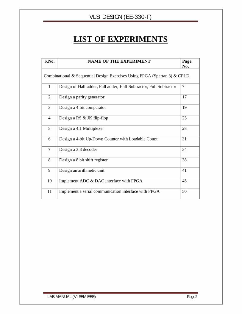
1 Design of Half adder, Full adder, Half Subtractor, Full Subtractor
7
2 Design a parity generator
17
3 Design a 4-bit comparator
19
4 Design a RS & JK flip-flop
23
5 Design a 4:1 Multiplexer
28
6 Design a 4-bit Up/Down Counter with Loadable Count
31
7 Design a 3:8 decoder
34
8 Design a 8 bit shift register
38
9 Design an arithmetic unit
41
10 Implement ADC & DAC interface with FPGA
45
11 Implement a serial communication interface with FPGA
50
VLSI DESIGN (EE-330-F)
LAB MANUAL (VI SEM EEE) Page3
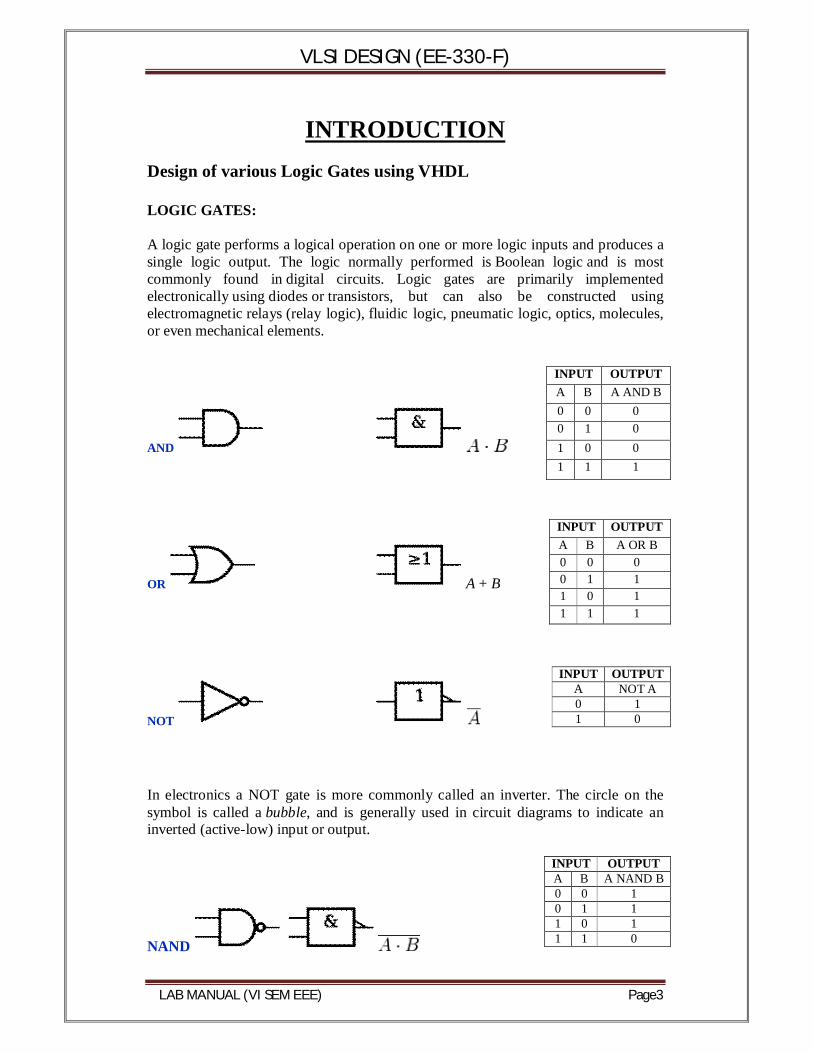
INTRODUCTION Design of various Logic Gates using VHDL LOGIC GATES: A logic gate performs a logical operation on one or more logic inputs and produces a single logic output. The logic normally performed is Boolean logic and is most commonly found in digital circuits. Logic gates are primarily implemented electronically using diodes or transistors, but can also be constructed using electromagnetic relays (relay logic), fluidic logic, pneumatic logic, optics, molecules, or even mechanical elements.
AND
OR A + B
NOT In electronics a NOT gate is more commonly called an inverter. The circle on the symbol is called a bubble, and is generally used in circuit diagrams to indicate an inverted (active-low) input or output.
NAND
INPUT OUTPUT A B A AND B 0 0 0 0 1 0 1 0 0 1 1 1
INPUT OUTPUT A B A OR B 0 0 0 0 1 1 1 0 1 1 1 1
INPUT OUTPUT A NOT A 0 1 1 0
INPUT OUTPUT A B A NAND B 0 0 1 0 1 1 1 0 1 1 1 0
VLSI DESIGN (EE-330-F)
LAB MANUAL (VI SEM EEE) Page4
NOR
XOR
XNOR or
INPUT OUTPUT A B A NOR B 0 0 1 0 1 0 1 0 0 1 1 0
INPUT OUTPUT A B A XOR B 0 0 0 0 1 1 1 0 1 1 1 0
INPUT OUTPUT A B A XNOR B 0 0 1 0 1 0 1 0 0 1 1 1
VLSI DESIGN (EE-330-F)
LAB MANUAL (VI SEM EEE) Page5
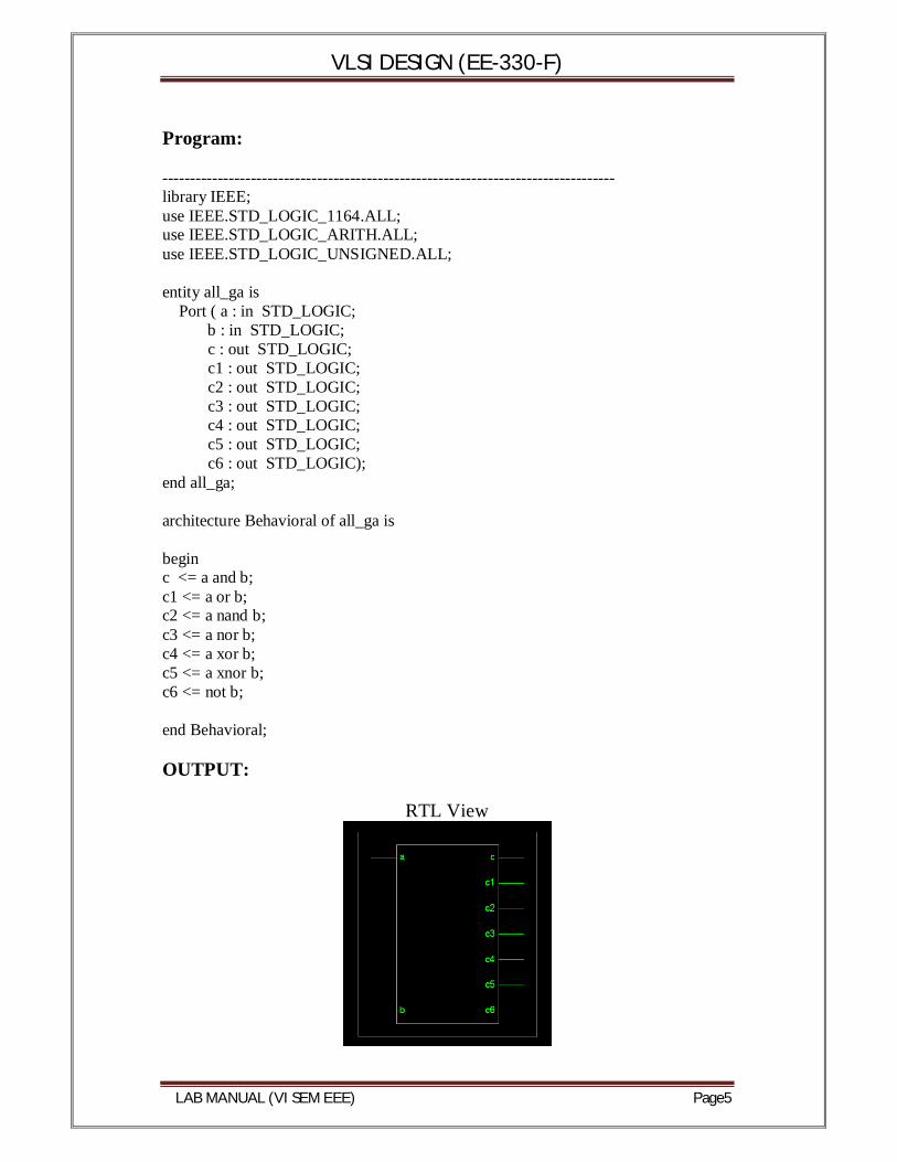
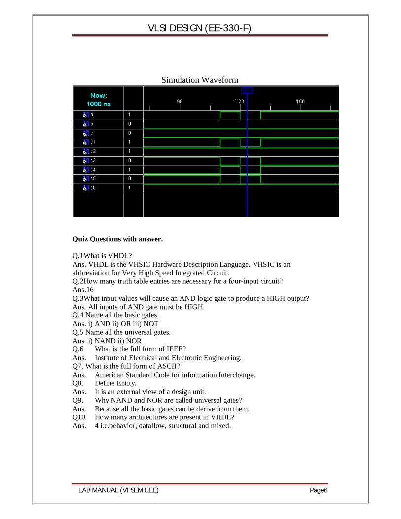
Program: ---------------------------------------------------------------------------------- library IEEE; use IEEE.STD_LOGIC_1164.ALL; use IEEE.STD_LOGIC_ARITH.ALL; use IEEE.STD_LOGIC_UNSIGNED.ALL; entity all_ga is Port ( a : in STD_LOGIC; b : in STD_LOGIC; c : out STD_LOGIC; c1 : out STD_LOGIC; c2 : out STD_LOGIC; c3 : out STD_LOGIC; c4 : out STD_LOGIC; c5 : out STD_LOGIC; c6 : out STD_LOGIC); end all_ga; architecture Behavioral of all_ga is begin c <= a and b; c1 <= a or b; c2 <= a nand b; c3 <= a nor b; c4 <= a xor b; c5 <= a xnor b; c6 <= not b; end Behavioral; OUTPUT:
RTL View
VLSI DESIGN (EE-330-F)
LAB MANUAL (VI SEM EEE) Page6
Simulation Waveform
Quiz Questions with answer.
Q.1What is VHDL? Ans. VHDL is the VHSIC Hardware Description Language. VHSIC is an abbreviation for Very High Speed Integrated Circuit. Q.2How many truth table entries are necessary for a four-input circuit? Ans.16 Q.3What input values will cause an AND logic gate to produce a HIGH output? Ans. All inputs of AND gate must be HIGH. Q.4 Name all the basic gates. Ans. i) AND ii) OR iii) NOT Q.5 Name all the universal gates. Ans .i) NAND ii) NOR Q.6 What is the full form of IEEE? Ans. Institute of Electrical and Electronic Engineering. Q7. What is the full form of ASCII? Ans. American Standard Code for information Interchange. Q8. Define Entity. Ans. It is an external view of a design unit. Q9. Why NAND and NOR are called universal gates? Ans. Because all the basic gates can be derive from them. Q10. How many architectures are present in VHDL? Ans. 4 i.e.behavior, dataflow, structural and mixed.
VLSI DESIGN (EE-330-F)
LAB MANUAL (VI SEM EEE) Page7
EXPERIMENT No. 1 Aim:- Design of Half adder, Full adder, Half Subtractor, Full Subtractor. Half adder A half adder is a logical circuit that performs an addition operation on two one-bit binary numbers often written as A and B. The half adder output is a sum of the two inputs usually represented with the signals Cout and S where
Following is the logic table and circuit diagram for half adder:
Inputs Outputs
A B C S
0 0 0 0
0 1 0 1
1 0 0 1
1 1 1 0
VLSI DESIGN (EE-330-F)
LAB MANUAL (VI SEM EEE) Page8
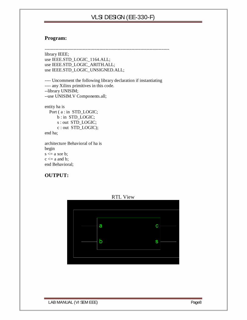
Program: ---------------------------------------------------------------------------------- library IEEE; use IEEE.STD_LOGIC_1164.ALL; use IEEE.STD_LOGIC_ARITH.ALL; use IEEE.STD_LOGIC_UNSIGNED.ALL; ---- Uncomment the following library declaration if instantiating ---- any Xilinx primitives in this code. --library UNISIM; --use UNISIM.V Components.all; entity ha is Port ( a : in STD_LOGIC; b : in STD_LOGIC; s : out STD_LOGIC; c : out STD_LOGIC); end ha; architecture Behavioral of ha is begin s <= a xor b; c <= a and b; end Behavioral; OUTPUT:
RTL View
VLSI DESIGN (EE-330-F)
LAB MANUAL (VI SEM EEE) Page9
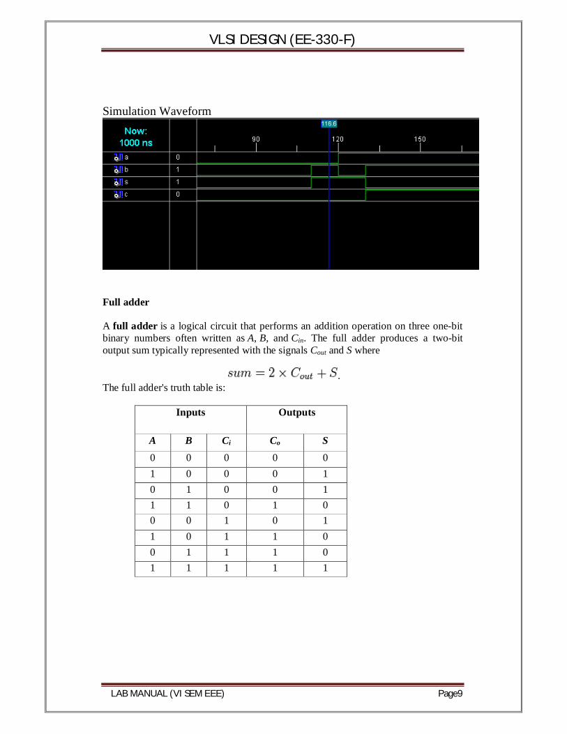
Simulation Waveform
Full adder A full adder is a logical circuit that performs an addition operation on three one-bit binary numbers often written as A, B, and Cin. The full adder produces a two-bit output sum typically represented with the signals Cout and S where
. The full adder's truth table is:
Inputs Outputs
A B Ci Co S 0 0 0 0 0 1 0 0 0 1 0 1 0 0 1 1 1 0 1 0 0 0 1 0 1 1 0 1 1 0 0 1 1 1 0 1 1 1 1 1
VLSI DESIGN (EE-330-F)
LAB MANUAL (VI SEM EEE) Page10
Program: ---------------------------------------------------------------------------------- library IEEE; use IEEE.STD_LOGIC_1164.ALL; use IEEE.STD_LOGIC_ARITH.ALL; use IEEE.STD_LOGIC_UNSIGNED.ALL; ---- Uncomment the following library declaration if instantiating ---- any Xilinx primitives in this code. --library UNISIM; --use UNISIM.VComponents.all; entity fa is Port ( a : in STD_LOGIC; b : in STD_LOGIC; cin : in STD_LOGIC; s : out STD_LOGIC; cout : out STD_LOGIC); end fa; architecture Behavioral of fa is begin s <= (a xor b) xor cin; cout <= (a and b) or (b and cin) or (a and cin); end Behavioral;
VLSI DESIGN (EE-330-F)
LAB MANUAL (VI SEM EEE) Page11
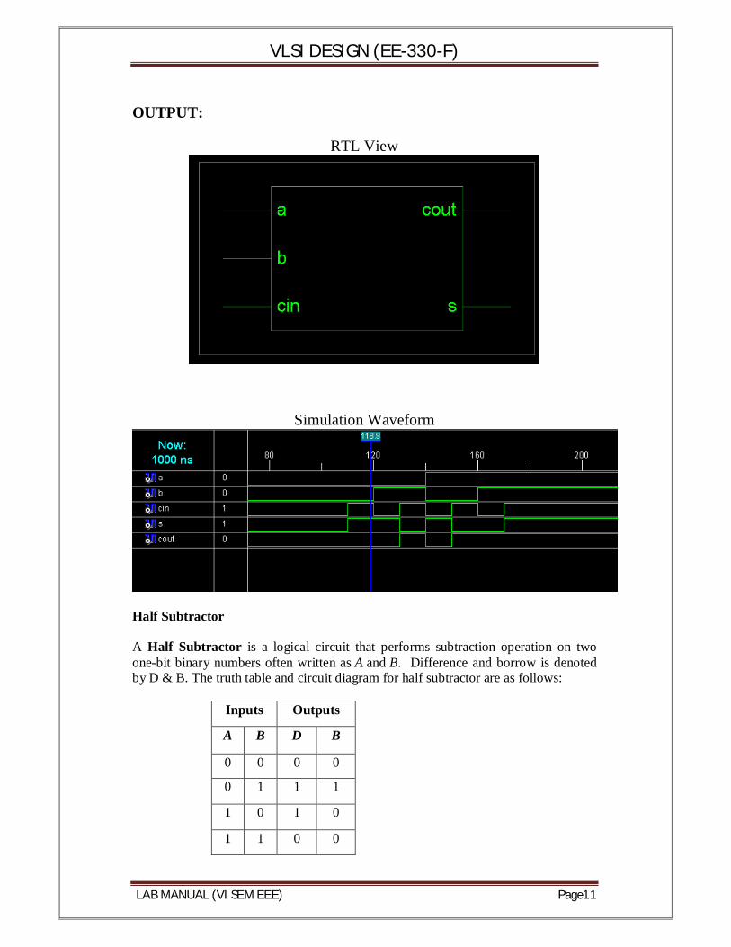
OUTPUT:
RTL View
Simulation Waveform
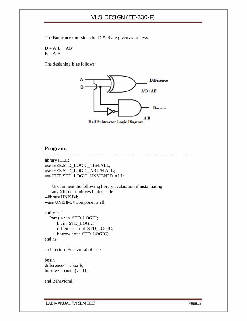
Half Subtractor A Half Subtractor is a logical circuit that performs subtraction operation on two one-bit binary numbers often written as A and B. Difference and borrow is denoted by D & B. The truth table and circuit diagram for half subtractor are as follows:
Inputs Outputs
A B D B
0 0 0 0
0 1 1 1
1 0 1 0
1 1 0 0
VLSI DESIGN (EE-330-F)
LAB MANUAL (VI SEM EEE) Page12
The Boolean expressions for D & B are given as follows: D = A’B + AB’ B = A’B The designing is as follows:
Program: -------------------------------------------------------------------------------------- library IEEE; use IEEE.STD_LOGIC_1164.ALL; use IEEE.STD_LOGIC_ARITH.ALL; use IEEE.STD_LOGIC_UNSIGNED.ALL; ---- Uncomment the following library declaration if instantiating ---- any Xilinx primitives in this code. --library UNISIM; --use UNISIM.VComponents.all; entity hs is Port ( a : in STD_LOGIC; b : in STD_LOGIC; difference : out STD_LOGIC; borrow : out STD_LOGIC); end hs; architecture Behavioral of hs is begin difference<= a xor b; borrow<= (not a) and b; end Behavioral;
VLSI DESIGN (EE-330-F)
LAB MANUAL (VI SEM EEE) Page13
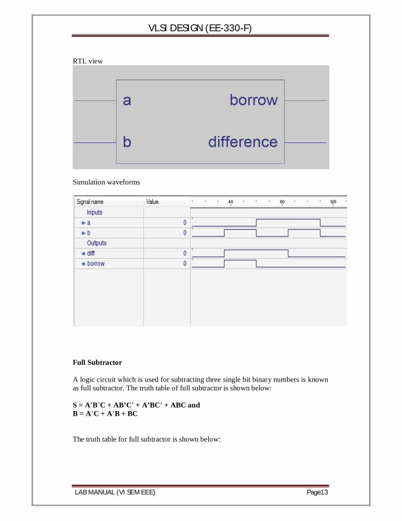
RTL view
Simulation waveforms
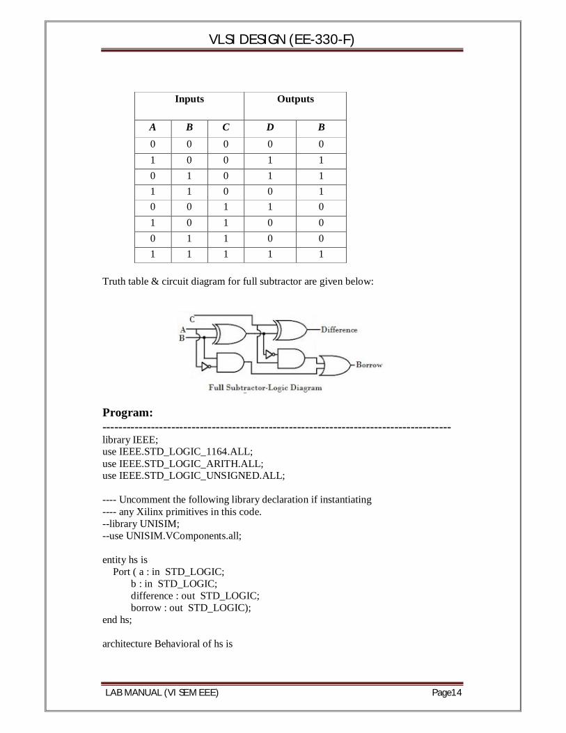
Full Subtractor A logic circuit which is used for subtracting three single bit binary numbers is known as full subtractor. The truth table of full subtractor is shown below: S = A’B’C + AB’C’ + A’BC’ + ABC and B = A’C + A’B + BC The truth table for full subtractor is shown below:
VLSI DESIGN (EE-330-F)
LAB MANUAL (VI SEM EEE) Page14
Inputs Outputs
A B C D B 0 0 0 0 0 1 0 0 1 1 0 1 0 1 1 1 1 0 0 1 0 0 1 1 0 1 0 1 0 0 0 1 1 0 0 1 1 1 1 1
Truth table & circuit diagram for full subtractor are given below:
Program: -------------------------------------------------------------------------------------- library IEEE; use IEEE.STD_LOGIC_1164.ALL; use IEEE.STD_LOGIC_ARITH.ALL; use IEEE.STD_LOGIC_UNSIGNED.ALL; ---- Uncomment the following library declaration if instantiating ---- any Xilinx primitives in this code. --library UNISIM; --use UNISIM.VComponents.all; entity hs is Port ( a : in STD_LOGIC; b : in STD_LOGIC; difference : out STD_LOGIC; borrow : out STD_LOGIC); end hs; architecture Behavioral of hs is
VLSI DESIGN (EE-330-F)
LAB MANUAL (VI SEM EEE) Page15
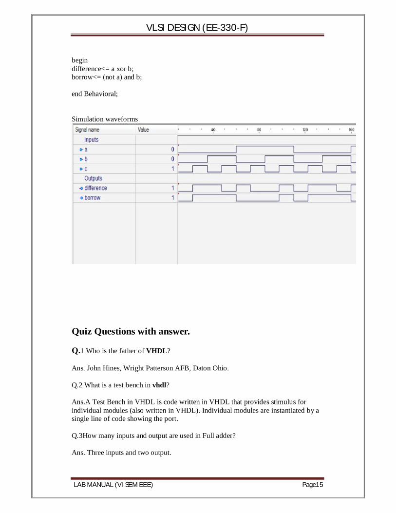
begin difference<= a xor b; borrow<= (not a) and b; end Behavioral; Simulation waveforms
Quiz Questions with answer.
Q.1 Who is the father of VHDL?
Ans. John Hines, Wright Patterson AFB, Daton Ohio.
Q.2 What is a test bench in vhdl?
Ans.A Test Bench in VHDL is code written in VHDL that provides stimulus for individual modules (also written in VHDL). Individual modules are instantiated by a single line of code showing the port.
Q.3How many inputs and output are used in Full adder?
Ans. Three inputs and two output.
VLSI DESIGN (EE-330-F)
LAB MANUAL (VI SEM EEE) Page16
Q.4 What are the advantages of designing?
Ans. Advantages of Designing:
1. Designing is useful in quick implementation, testing and useful in complex circuits.
2. Designing reduces the design cycle.
Q.5 Why HDL is used?
Ans.HDL is used because it is easy to design, implement, test and document increasingly complex digital system.
Q6. How many types of architecture in VHDL?
Ans: 4
Q7. What is the difference between sequential and combinational ckts.?
Ans: Seq ckts have memory cell inside it and combinational has no memory in it.
Q8. Is it possible to construct full adder using half adder?
Ans: Yes, by using two half adders.
Q9. How many i/ps required for half subtractor?
Ans: Two, difference and a borrow.
Q10. Is it possible to construct full subtractor using half subtractor?
Ans: Yes, by using two half subtractor.
VLSI DESIGN (EE-330-F)
LAB MANUAL (VI SEM EEE) Page17
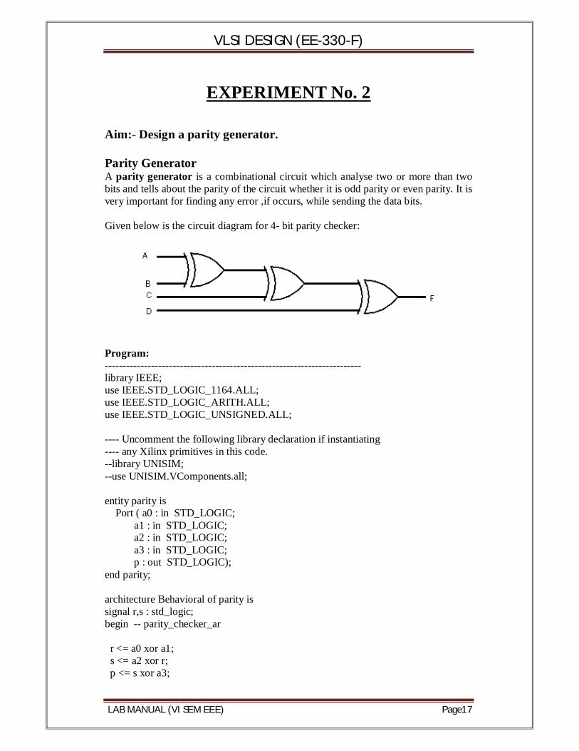
EXPERIMENT No. 2 Aim:- Design a parity generator. Parity Generator A parity generator is a combinational circuit which analyse two or more than two bits and tells about the parity of the circuit whether it is odd parity or even parity. It is very important for finding any error ,if occurs, while sending the data bits. Given below is the circuit diagram for 4- bit parity checker:
Program: ------------------------------------------------------------------------ library IEEE; use IEEE.STD_LOGIC_1164.ALL; use IEEE.STD_LOGIC_ARITH.ALL; use IEEE.STD_LOGIC_UNSIGNED.ALL; ---- Uncomment the following library declaration if instantiating ---- any Xilinx primitives in this code. --library UNISIM; --use UNISIM.VComponents.all; entity parity is Port ( a0 : in STD_LOGIC; a1 : in STD_LOGIC; a2 : in STD_LOGIC; a3 : in STD_LOGIC; p : out STD_LOGIC); end parity; architecture Behavioral of parity is signal r,s : std_logic; begin -- parity_checker_ar r <= a0 xor a1; s <= a2 xor r; p <= s xor a3;
VLSI DESIGN (EE-330-F)
LAB MANUAL (VI SEM EEE) Page18
end Behavioral; RTL View Simulation Waveforms
VLSI DESIGN (EE-330-F)
LAB MANUAL (VI SEM EEE) Page19
EXPERIMENT No. 3
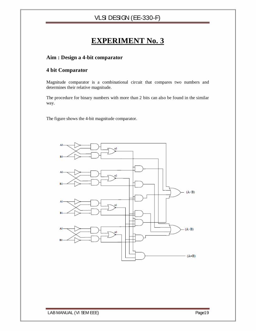
Aim : Design a 4-bit comparator 4 bit Comparator Magnitude comparator is a combinational circuit that compares two numbers and determines their relative magnitude. The procedure for binary numbers with more than 2 bits can also be found in the similar way. The figure shows the 4-bit magnitude comparator.
VLSI DESIGN (EE-330-F)
LAB MANUAL (VI SEM EEE) Page20
The truth table for 4-bit comparator is :
Program ----------------------------------------------------------------------- library IEEE; use IEEE.STD_LOGIC_1164.all; entity comparator_4bit is port( a : in STD_LOGIC_VECTOR(3 downto 0); b : in STD_LOGIC_VECTOR(3 downto 0); equal : out STD_LOGIC; greater : out STD_LOGIC; lower : out STD_LOGIC ); end comparator_4bit; architecture comparator_4bit_arc of comparator_4bit is begin comparator : process (a,b) is begin if (a=b) then equal <= '1'; greater <= '0'; lower <= '0'; elsif (a<b) then equal <= '0'; greater <= '0';
VLSI DESIGN (EE-330-F)
LAB MANUAL (VI SEM EEE) Page21
lower <= '1'; else equal <= '0'; greater <= '1'; lower <= '0'; end if; end process comparator; end comparator_4bit_arc; Simulation Waveforms
QUIZ questions
Q.1 Name the examples of combinational logic circuits. Ans. Examples of common combinational logic circuits include: half adders, full
adders, multiplexers, demultiplexers, encoders and decoders. One OR gate to OR CD and EF and next to OR of G & output of first OR
gate. Q.2 Which device converts BCD to Seven Segment ? Ans. A device which converts BCD to Seven Segment is called DECODER. Q.3 What is BCD to Seven segment decoder? Ans. A binary coded decimal (BCD) to 7-segment display decoder such as the
TTL 74LS47 or 74LS48, have 4 BCD inputs and 7 output lines, one for each LED segment. This allows a smaller 4-bit binary number (half a byte) to be used to display all the ternary numbers from 0 to 9 and by adding two displays together; a full range of numbers from 00 to 99 can be displayed with just a single byte of 8 data bits.
VLSI DESIGN (EE-330-F)
LAB MANUAL (VI SEM EEE) Page22
Q.4 What is decoder? Ans. A Decoder IC, is a device which converts one digital format into another and
the most commonly used device for doing this is the Binary Coded Decimal (BCD) to 7-Segment Display Decoder.
Q5: Q.5 What are the advantages of designing? Ans. Advantages of Designing: 1. Designing is useful in quick implementation, testing and useful in complex
circuits. 2. Designing reduces the design cycle. Q6: Write the applications of Encoder and decoder. Ans: They are used in communication systems. Q7: Name some encoders. Ans Priority encoder , 4:2 encoder and etc. Q8: How many i/ps are in 4:2 encoder? Ans 4 i/ps and 2 o/ps. Q9: How many select lines are present in 2:4 decoder? Ans none. Q10: How many outputs are present in 3:8 decoder? Ans. 8.
VLSI DESIGN (EE-330-F)
LAB MANUAL (VI SEM EEE) Page23
EXPERIMENT No. 4
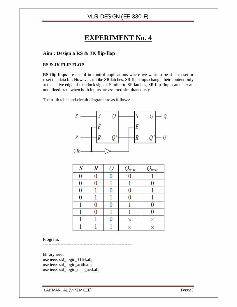
Aim : Design a RS & JK flip-flop RS & JK FLIP-FLOP RS flip-flops are useful in control applications where we want to be able to set or reset the data bit. However, unlike SR latches, SR flip-flops change their content only at the active edge of the clock signal. Similar to SR latches, SR flip-flops can enter an undefined state when both inputs are asserted simultaneously. The truth table and circuit diagram are as follows:
Program: ------------------------------------------------------------- library ieee; use ieee. std_logic_1164.all; use ieee. std_logic_arith.all; use ieee. std_logic_unsigned.all;
VLSI DESIGN (EE-330-F)
LAB MANUAL (VI SEM EEE) Page24
entity SR-FF is PORT( S,R,CLOCK,CLR,PRESET: in std_logic; Q, QBAR: out std_logic); end SR-FF; Architecture behavioral of SR-FF is begin P1: PROCESS(CLOCK,CLR,PRESET) variable x: std_logic; begin if(CLR='0') then x:='0'; elsif(PRESET='0')then x:='1'; elsif(CLOCK='1' and CLOCK'EVENT) then if(S='0' and R='0')then x:=x; elsif(S='1' and R='1')then x:='Z'; elsif(S='0' and R='1')then x:='0'; else x:='1'; end if; end if; Q<=x; QBAR<=not x; end PROCESS; end behavioral; Simulation Waveforms
VLSI DESIGN (EE-330-F)
LAB MANUAL (VI SEM EEE) Page25
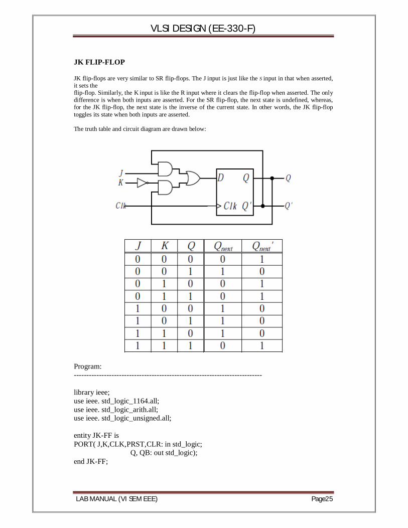
JK FLIP-FLOP JK flip-flops are very similar to SR flip-flops. The J input is just like the S input in that when asserted, it sets the flip-flop. Similarly, the K input is like the R input where it clears the flip-flop when asserted. The only difference is when both inputs are asserted. For the SR flip-flop, the next state is undefined, whereas, for the JK flip-flop, the next state is the inverse of the current state. In other words, the JK flip-flop toggles its state when both inputs are asserted. The truth table and circuit diagram are drawn below:
Program: --------------------------------------------------------------------------- library ieee; use ieee. std_logic_1164.all; use ieee. std_logic_arith.all; use ieee. std_logic_unsigned.all; entity JK-FF is PORT( J,K,CLK,PRST,CLR: in std_logic; Q, QB: out std_logic); end JK-FF;
VLSI DESIGN (EE-330-F)
LAB MANUAL (VI SEM EEE) Page26
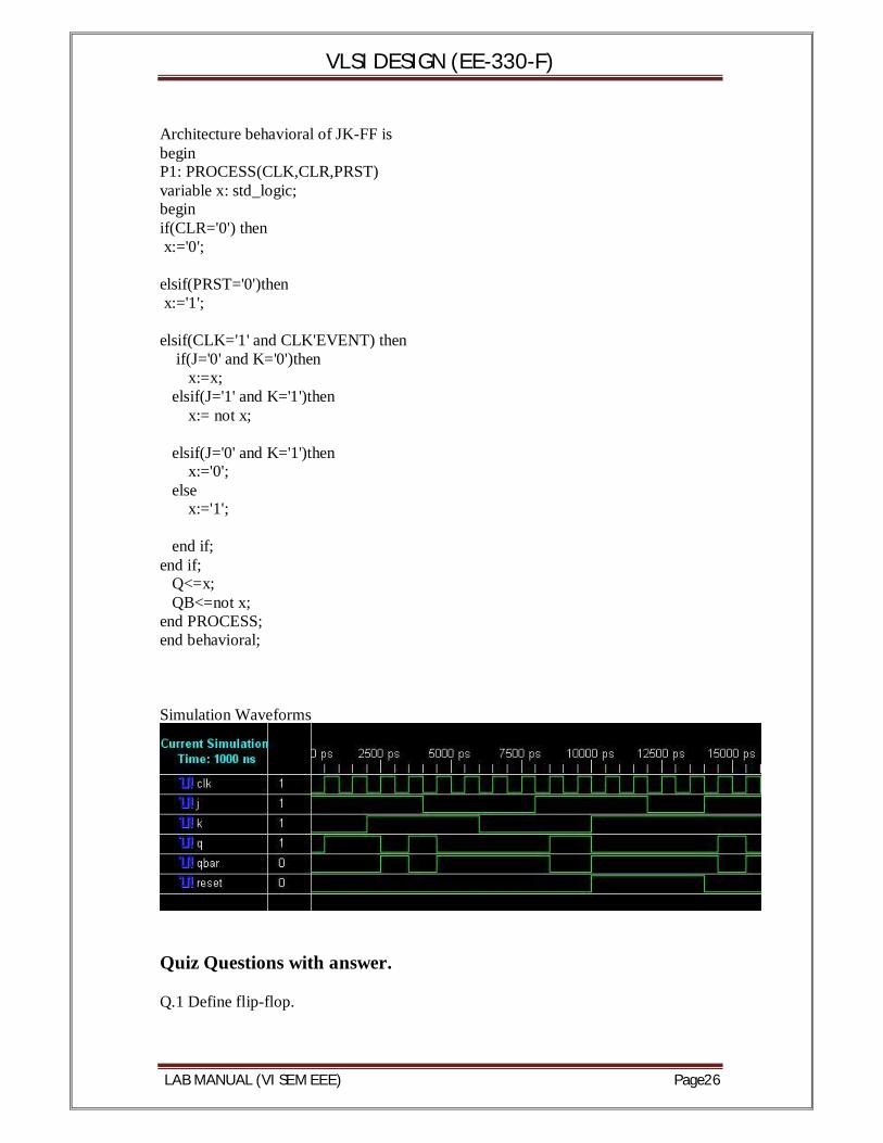
Architecture behavioral of JK-FF is begin P1: PROCESS(CLK,CLR,PRST) variable x: std_logic; begin if(CLR='0') then x:='0'; elsif(PRST='0')then x:='1'; elsif(CLK='1' and CLK'EVENT) then if(J='0' and K='0')then x:=x; elsif(J='1' and K='1')then x:= not x; elsif(J='0' and K='1')then x:='0'; else x:='1'; end if; end if; Q<=x; QB<=not x; end PROCESS; end behavioral; Simulation Waveforms
Quiz Questions with answer. Q.1 Define flip-flop.
VLSI DESIGN (EE-330-F)
LAB MANUAL (VI SEM EEE) Page27
Ans. A flip-flop is a device that can maintain binary information until it is directed by an input signal to change its state. There are several different types of flip-flops, the more commonly used are the D-FF and the JK-FF. Flip-flops are used in sequential circuit design. Q. 2The MSI chip 7474 is Ans. MSI chip 7474 dual edge triggered D Flip-Flop. Q. 3 How many flip-flops are required to construct mod 30 counter? Ans 5 Q.4The output of SR flip flop when S=1, R=0 is Ans As for the SR flip-flop S=set input R=reset input ,when S=1, R=0, Flip-flop will be set. Q.5 The number of flip flops contained in IC 7490 is Ans 2. Q6 What are the I/Ps of JK flip–flop where this race round condition occurs? Ans; .Both the inputs are 1 Q7: .Flip flop is astable or bistable? Ans Bistable. Q8: When RS flip-flop is said to be in a SET state? Ans. When the output is 1 Q9: What is the function of clock signal in flip-flop? Ans. To get the output at known time. Q10: What is the advantage of JK flip-flop over RS flip-flop? Ans. In RS flip-flop when both the inputs are 1 output is undetermined.
VLSI DESIGN (EE-330-F)
LAB MANUAL (VI SEM EEE) Page28
EXPERIMENT No. 5
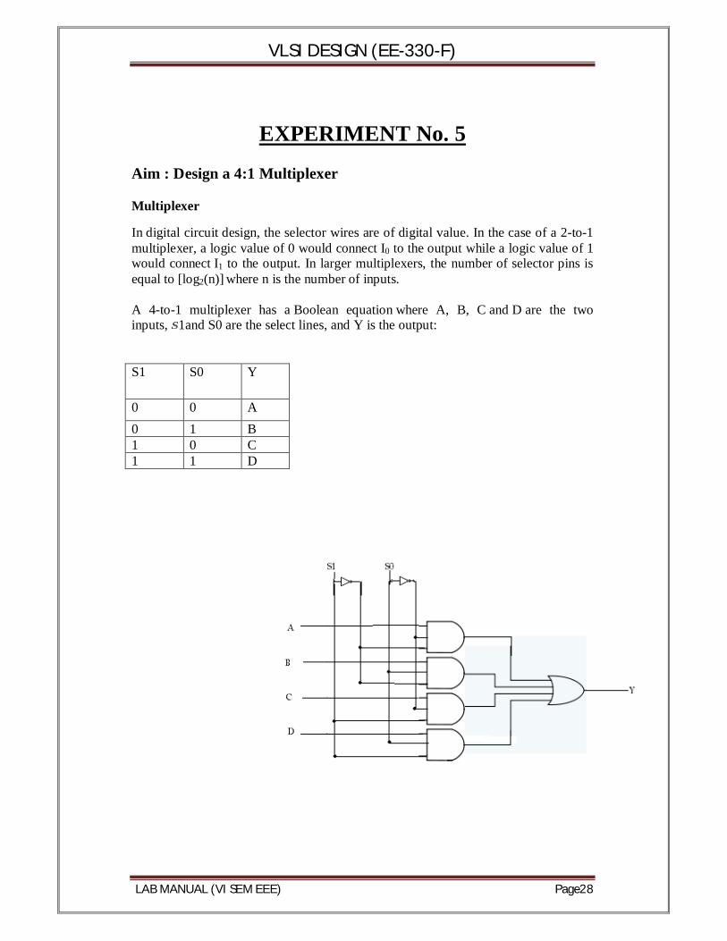
Aim : Design a 4:1 Multiplexer Multiplexer In digital circuit design, the selector wires are of digital value. In the case of a 2-to-1 multiplexer, a logic value of 0 would connect I0 to the output while a logic value of 1 would connect I1 to the output. In larger multiplexers, the number of selector pins is equal to [log2(n)] where n is the number of inputs. A 4-to-1 multiplexer has a Boolean equation where A, B, C and D are the two inputs, 1and S0 are the select lines, and Y is the output: S1 S0 Y
0 0 A 0 1 B 1 0 C 1 1 D
VLSI DESIGN (EE-330-F)
LAB MANUAL (VI SEM EEE) Page29
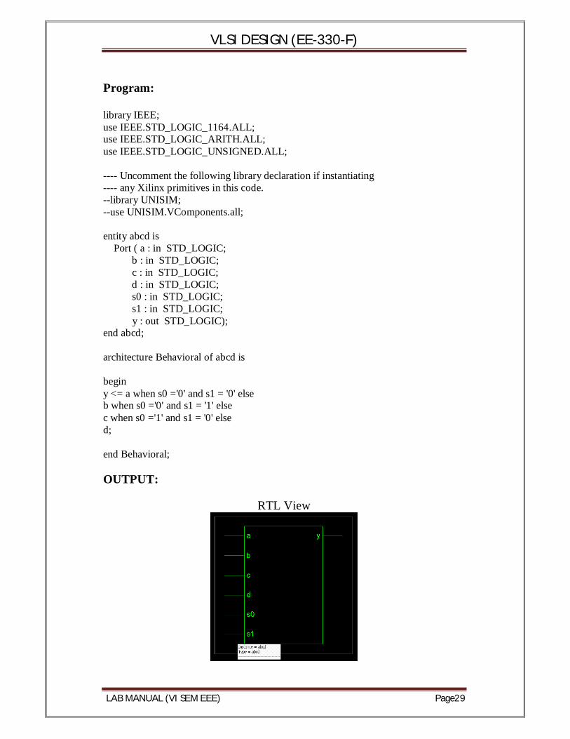
Program: library IEEE; use IEEE.STD_LOGIC_1164.ALL; use IEEE.STD_LOGIC_ARITH.ALL; use IEEE.STD_LOGIC_UNSIGNED.ALL; ---- Uncomment the following library declaration if instantiating ---- any Xilinx primitives in this code. --library UNISIM; --use UNISIM.VComponents.all; entity abcd is Port ( a : in STD_LOGIC; b : in STD_LOGIC; c : in STD_LOGIC; d : in STD_LOGIC; s0 : in STD_LOGIC; s1 : in STD_LOGIC; y : out STD_LOGIC); end abcd; architecture Behavioral of abcd is begin y <= a when s0 ='0' and s1 = '0' else b when s0 ='0' and s1 = '1' else c when s0 ='1' and s1 = '0' else d; end Behavioral; OUTPUT:
RTL View
VLSI DESIGN (EE-330-F)
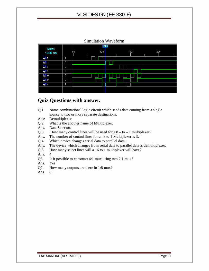
LAB MANUAL (VI SEM EEE) Page30
Simulation Waveform
Quiz Questions with answer. Q.1 Name combinational logic circuit which sends data coming from a single
source to two or more separate destinations. Ans: Demultiplexer Q.2 What is the another name of Multiplexer. Ans. Data Selector. Q.3 How many control lines will be used for a 8 – to – 1 multiplexer? Ans. The number of control lines for an 8 to 1 Multiplexer is 3. Q.4 Which device changes serial data to parallel data . Ans. The device which changes from serial data to parallel data is demultiplexer. Q.5 How many select lines will a 16 to 1 multiplexer will have? Ans. 4 Q6. Is it possible to construct 4:1 mux using two 2:1 mux? Ans. Yes Q7. How many outputs are there in 1:8 mux? Ans 8.
VLSI DESIGN (EE-330-F)
LAB MANUAL (VI SEM EEE) Page31
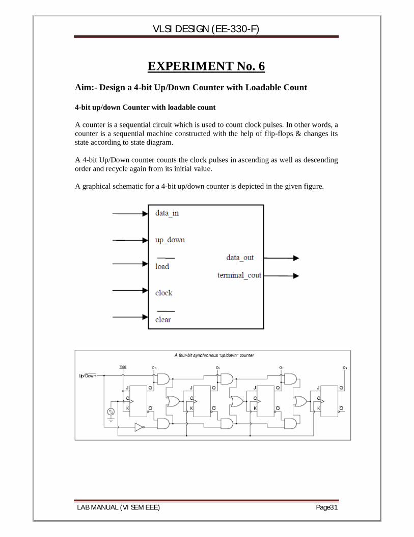
EXPERIMENT No. 6 Aim:- Design a 4-bit Up/Down Counter with Loadable Count 4-bit up/down Counter with loadable count A counter is a sequential circuit which is used to count clock pulses. In other words, a counter is a sequential machine constructed with the help of flip-flops & changes its state according to state diagram. A 4-bit Up/Down counter counts the clock pulses in ascending as well as descending order and recycle again from its initial value. A graphical schematic for a 4-bit up/down counter is depicted in the given figure.
VLSI DESIGN (EE-330-F)
LAB MANUAL (VI SEM EEE) Page32
Program: ----------------------------------------------------------------------------- ENTITY counter_4bit IS PORT( data_in: IN std_logic_vector(3 downto 0); clock: IN std_logic; load: IN std_logic; clear: IN std_logic; up_down: IN std_logic; terminal_count: OUT std_logic; data_out: OUT std_logic_vector (3 downto 0)); END counter_4bit; ARCHITECTURE counter_4bit_arh OF counter_4bit IS SIGNAL count:std_logic_vector(3 downto 0) :="0000"; BEGIN PROCESS (clock) BEGIN IF (clear = '0') THEN count <= "0000"; ELSIF(load = '0') THEN count <= data_in; ELSE IF (clock'EVENT AND clock = '0') AND(clock'LAST_VALUE = '1') THEN IF(up_down = '1') THEN count <= count + 1; END IF; IF(up_down = '0') THEN count <= count - 1; END IF; END IF; END IF; IF (count = "1111") THEN terminal_count <= '1'; ELSE terminal_count <= '0'; END IF; data_out <= count; END PROCESS; END counter_4bit_arh;
VLSI DESIGN (EE-330-F)
LAB MANUAL (VI SEM EEE) Page33
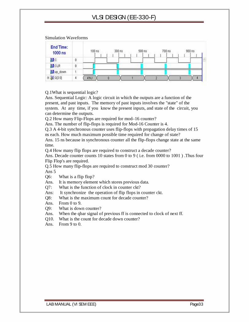
Simulation Waveforms
Q.1What is sequential logic? Ans. Sequential Logic: A logic circuit in which the outputs are a function of the present, and past inputs. The memory of past inputs involves the "state" of the system. At any time, if you know the present inputs, and state of the circuit, you can determine the outputs. Q.2 How many Flip-Flops are required for mod–16 counter? Ans. The number of flip-flops is required for Mod-16 Counter is 4. Q.3 A 4-bit synchronous counter uses flip-flops with propagation delay times of 15 ns each. How much maximum possible time required for change of state? Ans. 15 ns because in synchronous counter all the flip-flops change state at the same time. Q.4 How many flip flops are required to construct a decade counter? Ans. Decade counter counts 10 states from 0 to 9 ( i.e. from 0000 to 1001 ) .Thus four Flip Flop's are required. Q.5 How many flip-flops are required to construct mod 30 counter? Ans 5 Q6: What is a flip flop? Ans. It is memory element which stores previous data. Q7: What is the function of clock in counter ckt? Ans: It synchronize the operation of flip flops in counter ckt. Q8: What is the maximum count for decade counter? Ans. From 0 to 9. Q9: What is down counter? Ans. When the qbar signal of previous ff is connected to clock of next ff. Q10. What is the count for decade down counter? Ans. From 9 to 0.
VLSI DESIGN (EE-330-F)
LAB MANUAL (VI SEM EEE) Page34
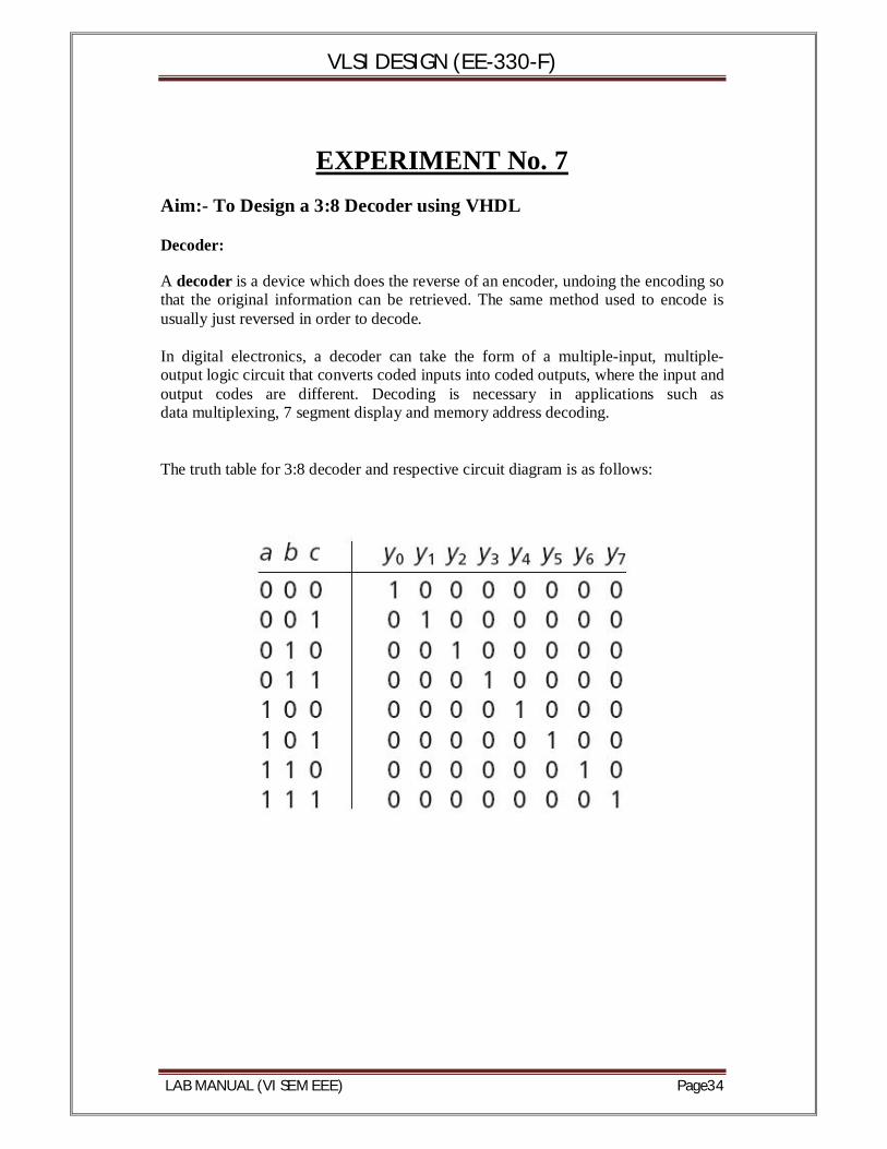
EXPERIMENT No. 7 Aim:- To Design a 3:8 Decoder using VHDL Decoder: A decoder is a device which does the reverse of an encoder, undoing the encoding so that the original information can be retrieved. The same method used to encode is usually just reversed in order to decode. In digital electronics, a decoder can take the form of a multiple-input, multiple-output logic circuit that converts coded inputs into coded outputs, where the input and output codes are different. Decoding is necessary in applications such as data multiplexing, 7 segment display and memory address decoding. The truth table for 3:8 decoder and respective circuit diagram is as follows:
VLSI DESIGN (EE-330-F)
LAB MANUAL (VI SEM EEE) Page35
VLSI DESIGN (EE-330-F)
LAB MANUAL (VI SEM EEE) Page36
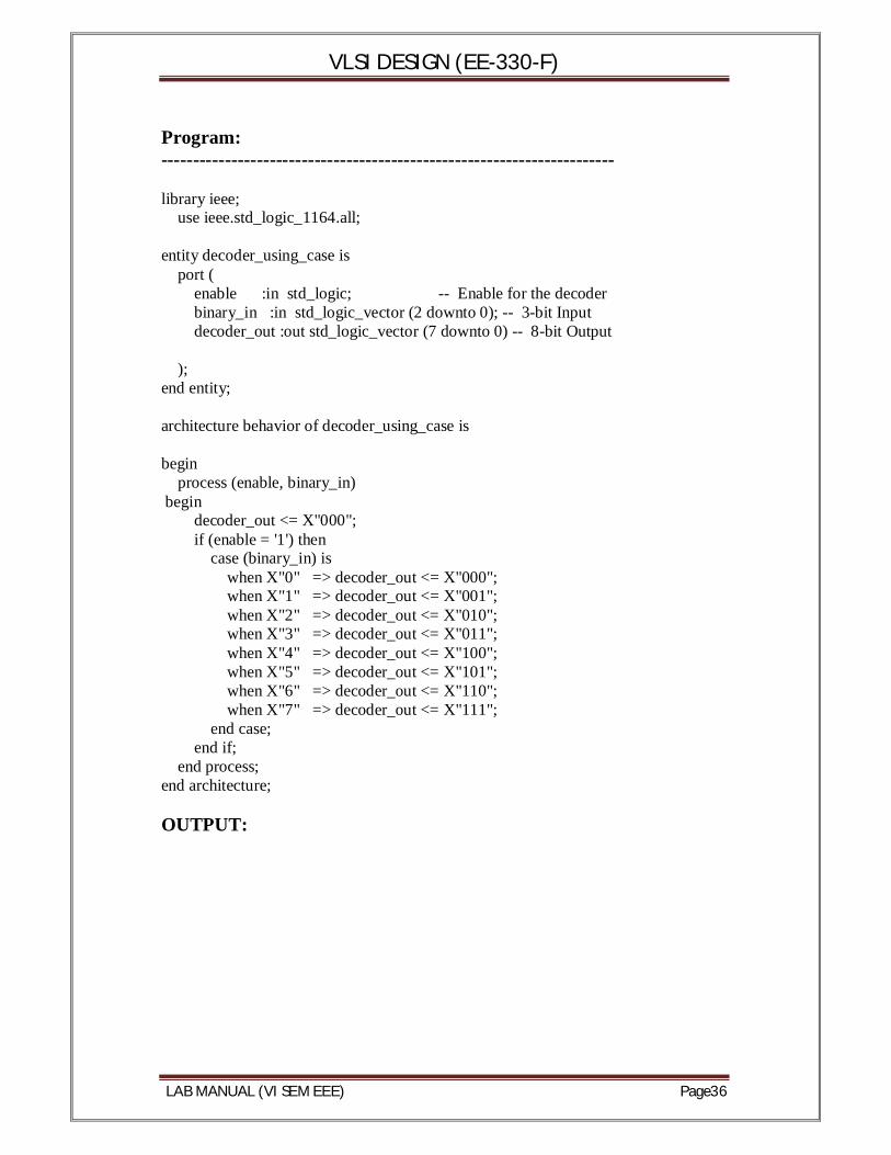
Program: ----------------------------------------------------------------------- library ieee; use ieee.std_logic_1164.all; entity decoder_using_case is port ( enable :in std_logic; -- Enable for the decoder binary_in :in std_logic_vector (2 downto 0); -- 3-bit Input decoder_out :out std_logic_vector (7 downto 0) -- 8-bit Output ); end entity; architecture behavior of decoder_using_case is begin process (enable, binary_in) begin decoder_out <= X"000"; if (enable = '1') then case (binary_in) is when X"0" => decoder_out <= X"000"; when X"1" => decoder_out <= X"001"; when X"2" => decoder_out <= X"010"; when X"3" => decoder_out <= X"011"; when X"4" => decoder_out <= X"100"; when X"5" => decoder_out <= X"101"; when X"6" => decoder_out <= X"110"; when X"7" => decoder_out <= X"111"; end case; end if; end process; end architecture; OUTPUT:
VLSI DESIGN (EE-330-F)
LAB MANUAL (VI SEM EEE) Page37
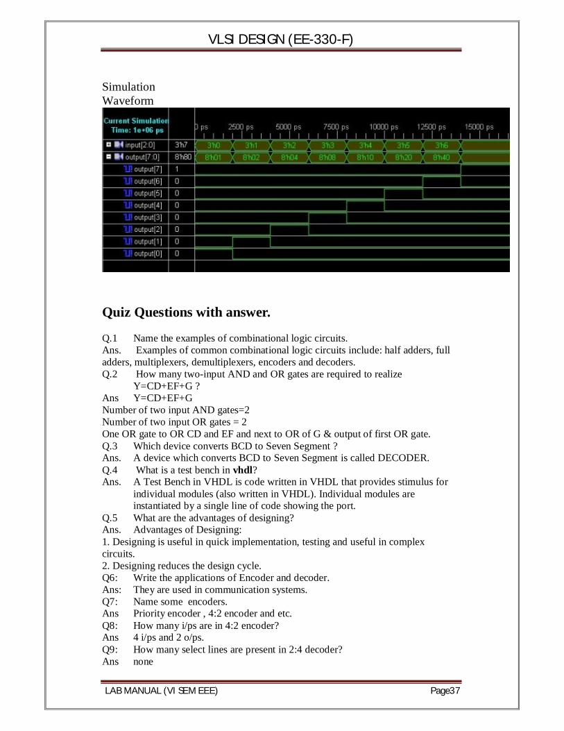
Simulation Waveform
Quiz Questions with answer. Q.1 Name the examples of combinational logic circuits. Ans. Examples of common combinational logic circuits include: half adders, full adders, multiplexers, demultiplexers, encoders and decoders. Q.2 How many two-input AND and OR gates are required to realize
Y=CD+EF+G ? Ans Y=CD+EF+G Number of two input AND gates=2 Number of two input OR gates = 2 One OR gate to OR CD and EF and next to OR of G & output of first OR gate. Q.3 Which device converts BCD to Seven Segment ? Ans. A device which converts BCD to Seven Segment is called DECODER. Q.4 What is a test bench in vhdl? Ans. A Test Bench in VHDL is code written in VHDL that provides stimulus for
individual modules (also written in VHDL). Individual modules are instantiated by a single line of code showing the port.
Q.5 What are the advantages of designing? Ans. Advantages of Designing: 1. Designing is useful in quick implementation, testing and useful in complex circuits. 2. Designing reduces the design cycle. Q6: Write the applications of Encoder and decoder. Ans: They are used in communication systems. Q7: Name some encoders. Ans Priority encoder , 4:2 encoder and etc. Q8: How many i/ps are in 4:2 encoder? Ans 4 i/ps and 2 o/ps. Q9: How many select lines are present in 2:4 decoder? Ans none
VLSI DESIGN (EE-330-F)
LAB MANUAL (VI SEM EEE) Page38
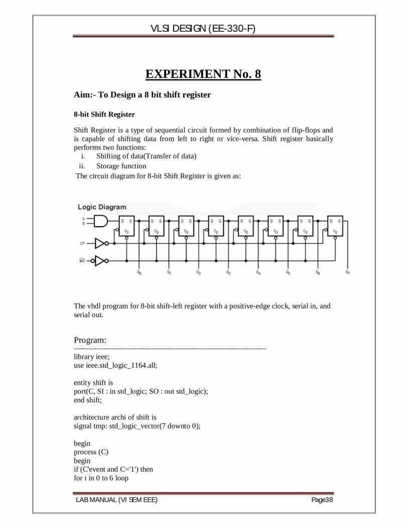
EXPERIMENT No. 8 Aim:- To Design a 8 bit shift register 8-bit Shift Register Shift Register is a type of sequential circuit formed by combination of flip-flops and is capable of shifting data from left to right or vice-versa. Shift register basically performs two functions:
i. Shifting of data(Transfer of data) ii. Storage function
The circuit diagram for 8-bit Shift Register is given as:
The vhdl program for 8-bit shift-left register with a positive-edge clock, serial in, and serial out. Program: -------------------------------------------------------------------------------------------- library ieee; use ieee.std_logic_1164.all; entity shift is port(C, SI : in std_logic; SO : out std_logic); end shift; architecture archi of shift is signal tmp: std_logic_vector(7 downto 0); begin process (C) begin if (C'event and C='1') then for i in 0 to 6 loop
VLSI DESIGN (EE-330-F)
LAB MANUAL (VI SEM EEE) Page39
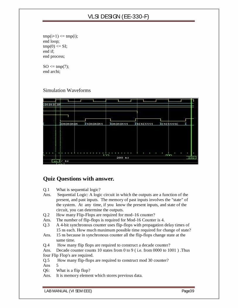
tmp(i+1) <= tmp(i); end loop; tmp(0) <= SI; end if; end process; SO <= tmp(7); end archi; Simulation Waveforms
Quiz Questions with answer. Q.1 What is sequential logic? Ans. Sequential Logic: A logic circuit in which the outputs are a function of the
present, and past inputs. The memory of past inputs involves the "state" of the system. At any time, if you know the present inputs, and state of the circuit, you can determine the outputs.
Q.2 How many Flip-Flops are required for mod–16 counter? Ans. The number of flip-flops is required for Mod-16 Counter is 4. Q.3 A 4-bit synchronous counter uses flip-flops with propagation delay times of
15 ns each. How much maximum possible time required for change of state? Ans. 15 ns because in synchronous counter all the flip-flops change state at the
same time. Q.4 How many flip flops are required to construct a decade counter? Ans. Decade counter counts 10 states from 0 to 9 ( i.e. from 0000 to 1001 ) .Thus four Flip Flop's are required. Q.5 How many flip-flops are required to construct mod 30 counter? Ans 5 Q6: What is a flip flop? Ans. It is memory element which stores previous data.
VLSI DESIGN (EE-330-F)
LAB MANUAL (VI SEM EEE) Page40
Q7: What is the function of clock in counter ckt? Ans: It synchronize the operation of flip flops in counter ckt. Q8: What is the maximum count for decade counter? Ans. From 0 to 9. Q9: What is down counter? Ans. When the qbar signal of previous ff is connected to clock of next ff. Q10. What is the count for decade down counter? Ans. From 9 to 0.
VLSI DESIGN (EE-330-F)
LAB MANUAL (VI SEM EEE) Page41
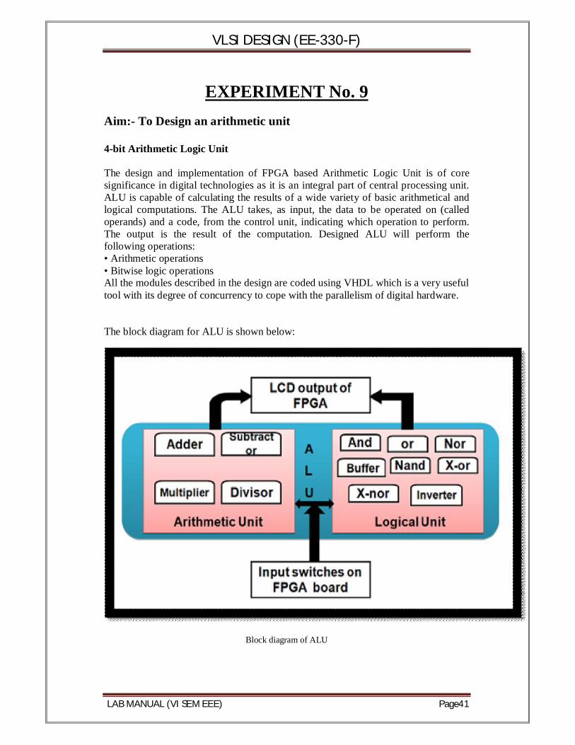
EXPERIMENT No. 9 Aim:- To Design an arithmetic unit 4-bit Arithmetic Logic Unit The design and implementation of FPGA based Arithmetic Logic Unit is of core significance in digital technologies as it is an integral part of central processing unit. ALU is capable of calculating the results of a wide variety of basic arithmetical and logical computations. The ALU takes, as input, the data to be operated on (called operands) and a code, from the control unit, indicating which operation to perform. The output is the result of the computation. Designed ALU will perform the following operations: • Arithmetic operations • Bitwise logic operations All the modules described in the design are coded using VHDL which is a very useful tool with its degree of concurrency to cope with the parallelism of digital hardware. The block diagram for ALU is shown below:
Block diagram of ALU
VLSI DESIGN (EE-330-F)
LAB MANUAL (VI SEM EEE) Page42
There are two kinds of operation which an ALU can perform first part deals with arithmetic computations and is referred to as Arithmetic Unit. It is capable of addition, subtraction, multiplication, division, increment and decrement. The second part deals with the Gated results in the shape of AND, OR, XOR, inverter, rotate, left shift and right shift, which is referred to as Logic Unit. The functions are controlled and executed by selecting operation or control bits. Program: ------------------------------------------------------------------------- library IEEE; use IEEE.STD_LOGIC_1164.ALL; use IEEE.STD_LOGIC_ARITH.ALL; use IEEE.STD_LOGIC_UNSIGNED.ALL; entity alu is Port ( a : in STD_LOGIC_VECTOR (03 downto 0); b : in STD_LOGIC_VECTOR (03 downto 0); opcode : in STD_LOGIC_VECTOR (03 downto 0); y : out STD_LOGIC_VECTOR (03 downto 0)); end alu; Architecture Behavioral of alu is begin with opcode (3 downto 0) select y<= a when "0000", (not a) when "0001", b when "0010", (not b) when "0011", a and b when "0100", a or b when "0101", a nand b when "0110", a nor b when "0111", a xor b when "1000", a+1 when"1001", b+1 when "1010", a+b when "1011", a-1 when "1100", b-1 when "1101", a-b when "1110", a xnor b when "1111", "0000" when others; end Behavioral;
VLSI DESIGN (EE-330-F)
LAB MANUAL (VI SEM EEE) Page43
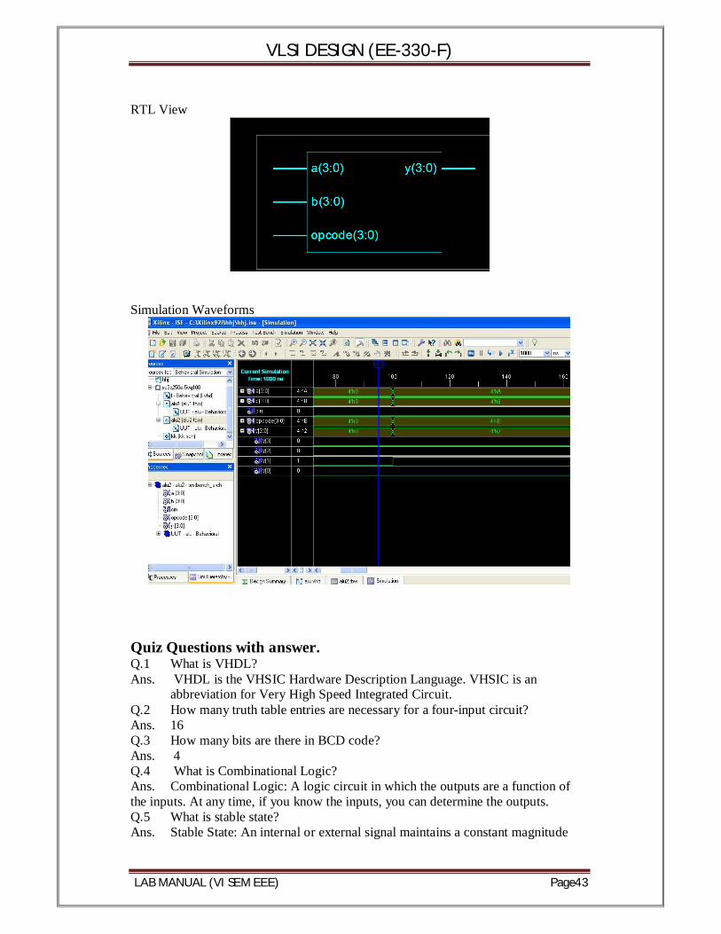
RTL View
Simulation Waveforms
Quiz Questions with answer. Q.1 What is VHDL? Ans. VHDL is the VHSIC Hardware Description Language. VHSIC is an
abbreviation for Very High Speed Integrated Circuit. Q.2 How many truth table entries are necessary for a four-input circuit? Ans. 16 Q.3 How many bits are there in BCD code? Ans. 4 Q.4 What is Combinational Logic? Ans. Combinational Logic: A logic circuit in which the outputs are a function of the inputs. At any time, if you know the inputs, you can determine the outputs. Q.5 What is stable state? Ans. Stable State: An internal or external signal maintains a constant magnitude
VLSI DESIGN (EE-330-F)
LAB MANUAL (VI SEM EEE) Page44
(or specified range or function) for a period of time determined by external input signals. Q6. What is BCD to Gray converter? Ans: The converter which converts bcd code into gray code. Q7: What is the application of above code converter? Ans We use in communication systems. Q8. BCD to Gray converter is a combinational or sequential ckt? Ans. Combinational ckt. Q9: Write down the method of Binary to Gray conversion. Ans: Using the Ex-Or gates Q10: Convert 0101 to Decimal. Ans; 5
VLSI DESIGN (EE-330-F)
LAB MANUAL (VI SEM EEE) Page45
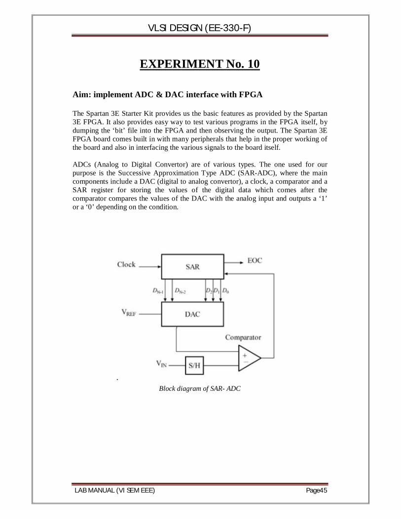
EXPERIMENT No. 10 Aim: implement ADC & DAC interface with FPGA The Spartan 3E Starter Kit provides us the basic features as provided by the Spartan 3E FPGA. It also provides easy way to test various programs in the FPGA itself, by dumping the ‘bit’ file into the FPGA and then observing the output. The Spartan 3E FPGA board comes built in with many peripherals that help in the proper working of the board and also in interfacing the various signals to the board itself. ADCs (Analog to Digital Convertor) are of various types. The one used for our purpose is the Successive Approximation Type ADC (SAR-ADC), where the main components include a DAC (digital to analog convertor), a clock, a comparator and a SAR register for storing the values of the digital data which comes after the comparator compares the values of the DAC with the analog input and outputs a ‘1’ or a ‘0’ depending on the condition.
Block diagram of SAR- ADC
VLSI DESIGN (EE-330-F)
LAB MANUAL (VI SEM EEE) Page46
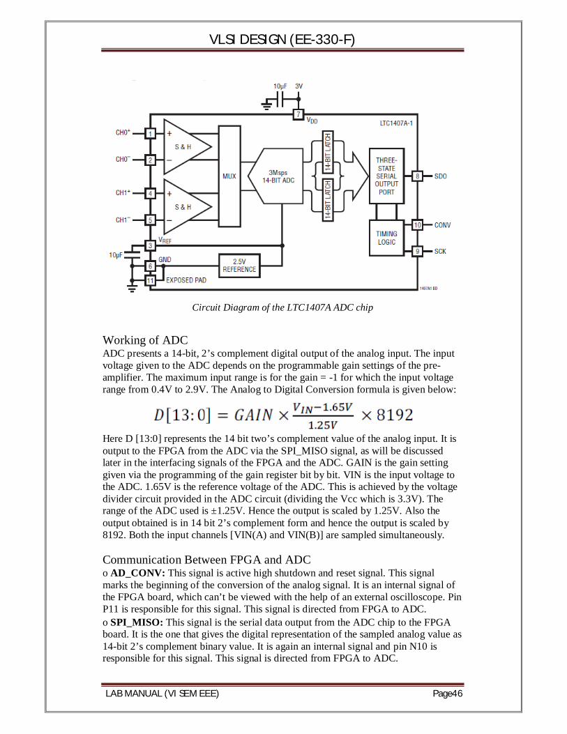
Circuit Diagram of the LTC1407A ADC chip
Working of ADC ADC presents a 14-bit, 2’s complement digital output of the analog input. The input voltage given to the ADC depends on the programmable gain settings of the pre-amplifier. The maximum input range is for the gain = -1 for which the input voltage range from 0.4V to 2.9V. The Analog to Digital Conversion formula is given below:
Here D [13:0] represents the 14 bit two’s complement value of the analog input. It is output to the FPGA from the ADC via the SPI_MISO signal, as will be discussed later in the interfacing signals of the FPGA and the ADC. GAIN is the gain setting given via the programming of the gain register bit by bit. VIN is the input voltage to the ADC. 1.65V is the reference voltage of the ADC. This is achieved by the voltage divider circuit provided in the ADC circuit (dividing the Vcc which is 3.3V). The range of the ADC used is ±1.25V. Hence the output is scaled by 1.25V. Also the output obtained is in 14 bit 2’s complement form and hence the output is scaled by 8192. Both the input channels [VIN(A) and VIN(B)] are sampled simultaneously. Communication Between FPGA and ADC o AD_CONV: This signal is active high shutdown and reset signal. This signal marks the beginning of the conversion of the analog signal. It is an internal signal of the FPGA board, which can’t be viewed with the help of an external oscilloscope. Pin P11 is responsible for this signal. This signal is directed from FPGA to ADC. o SPI_MISO: This signal is the serial data output from the ADC chip to the FPGA board. It is the one that gives the digital representation of the sampled analog value as 14-bit 2’s complement binary value. It is again an internal signal and pin N10 is responsible for this signal. This signal is directed from FPGA to ADC.
VLSI DESIGN (EE-330-F)
LAB MANUAL (VI SEM EEE) Page47
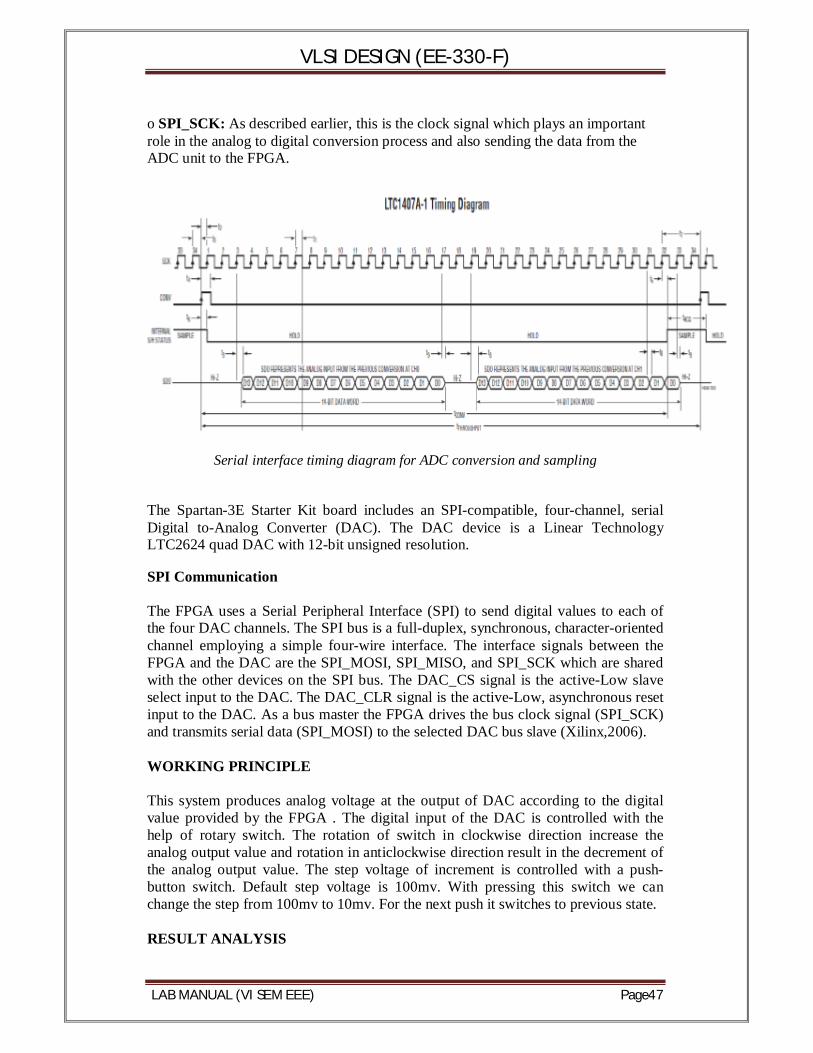
o SPI_SCK: As described earlier, this is the clock signal which plays an important role in the analog to digital conversion process and also sending the data from the ADC unit to the FPGA.
Serial interface timing diagram for ADC conversion and sampling
The Spartan-3E Starter Kit board includes an SPI-compatible, four-channel, serial Digital to-Analog Converter (DAC). The DAC device is a Linear Technology LTC2624 quad DAC with 12-bit unsigned resolution. SPI Communication The FPGA uses a Serial Peripheral Interface (SPI) to send digital values to each of the four DAC channels. The SPI bus is a full-duplex, synchronous, character-oriented channel employing a simple four-wire interface. The interface signals between the FPGA and the DAC are the SPI_MOSI, SPI_MISO, and SPI_SCK which are shared with the other devices on the SPI bus. The DAC_CS signal is the active-Low slave select input to the DAC. The DAC_CLR signal is the active-Low, asynchronous reset input to the DAC. As a bus master the FPGA drives the bus clock signal (SPI_SCK) and transmits serial data (SPI_MOSI) to the selected DAC bus slave (Xilinx,2006). WORKING PRINCIPLE This system produces analog voltage at the output of DAC according to the digital value provided by the FPGA . The digital input of the DAC is controlled with the help of rotary switch. The rotation of switch in clockwise direction increase the analog output value and rotation in anticlockwise direction result in the decrement of the analog output value. The step voltage of increment is controlled with a push-button switch. Default step voltage is 100mv. With pressing this switch we can change the step from 100mv to 10mv. For the next push it switches to previous state. RESULT ANALYSIS
VLSI DESIGN (EE-330-F)
LAB MANUAL (VI SEM EEE) Page48
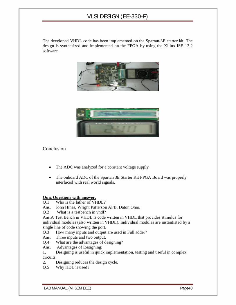
The developed VHDL code has been implemented on the Spartan-3E starter kit. The design is synthesized and implemented on the FPGA by using the Xilinx ISE 13.2 software.
Conclusion
The ADC was analyzed for a constant voltage supply.
The onboard ADC of the Spartan 3E Starter Kit FPGA Board was properly interfaced with real world signals.
Quiz Questions with answer. Q.1 Who is the father of VHDL? Ans. John Hines, Wright Patterson AFB, Daton Ohio. Q.2 What is a testbench in vhdl? Ans.A Test Bench in VHDL is code written in VHDL that provides stimulus for individual modules (also written in VHDL). Individual modules are instantiated by a single line of code showing the port. Q.3 How many inputs and output are used in Full adder? Ans. Three inputs and two output. Q.4 What are the advantages of designing? Ans. Advantages of Designing: 1. Designing is useful in quick implementation, testing and useful in complex circuits. 2. Designing reduces the design cycle. Q.5 Why HDL is used?
VLSI DESIGN (EE-330-F)
LAB MANUAL (VI SEM EEE) Page49
Ans. HDL is used because it is easy to design, implement, test and document increasingly complex digital system. Q6. Give the basic rules for binary addition? Ans. 0+0 = 0; 0+1 = 1 ; 1+1 = 1 0 ; 1+0 = 1. Q7: What is the drawback of half adder? Ans: We can’t add carry bit from previous stage. Q8: What is the difference b/w half adder& half sub tractor? Ans: Half adder can add two bits & half sub tractor can subtract two bits. Q9: Define Nibble? Ans. Combination of four bits
VLSI DESIGN (EE-330-F)
LAB MANUAL (VI SEM EEE) Page50
EXPERIMENT No. 11
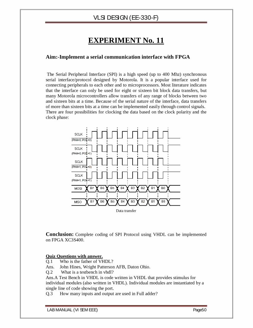
Aim:-Implement a serial communication interface with FPGA The Serial Peripheral Interface (SPI) is a high speed (up to 400 Mhz) synchronous serial interface/protocol designed by Motorola. It is a popular interface used for connecting peripherals to each other and to microprocessors. Most literature indicates that the interface can only be used for eight or sixteen bit block data transfers, but many Motorola microcontrollers allow transfers of any range of blocks between two and sixteen bits at a time. Because of the serial nature of the interface, data transfers of more than sixteen bits at a time can be implemented easily through control signals. There are four possibilities for clocking the data based on the clock polarity and the clock phase:
Data transfer
Conclusion: Complete coding of SPI Protocol using VHDL can be implemented on FPGA XC3S400. Quiz Questions with answer. Q.1 Who is the father of VHDL? Ans. John Hines, Wright Patterson AFB, Daton Ohio. Q.2 What is a testbench in vhdl? Ans.A Test Bench in VHDL is code written in VHDL that provides stimulus for individual modules (also written in VHDL). Individual modules are instantiated by a single line of code showing the port. Q.3 How many inputs and output are used in Full adder?
VLSI DESIGN (EE-330-F)
LAB MANUAL (VI SEM EEE) Page51
Ans. Three inputs and two output. Q.4 What are the advantages of designing? Ans. Advantages of Designing: 1. Designing is useful in quick implementation, testing and useful in complex circuits. 2. Designing reduces the design cycle. Q.5 Why HDL is used? Ans. HDL is used because it is easy to design, implement, test and document increasingly complex digital system. Q6. Give the basic rules for binary addition? Ans. 0+0 = 0; 0+1 = 1 ; 1+1 = 1 0 ; 1+0 = 1. Q7: What is the drawback of half adder? Ans: We can’t add carry bit from previous stage. Q8: What is the difference b/w half adder& half sub tractor? Ans: Half adder can add two bits & half sub tractor can subtract two bits. Q9: Define Nibble? Ans. Combination of four bits