30
VLSI Design Lecture 3a: Nonideal Transistors
| Date post: | 17-Dec-2015 |
| Category: |
Documents |
| Upload: | angel-wright |
| View: | 227 times |
| Download: | 1 times |
VLSI Design
Lecture 3a: Nonideal Transistors
Outline
Transistor I-V Review Nonideal Transistor Behavior
Velocity Saturation Channel Length Modulation Body Effect Leakage Temperature Sensitivity
Process and Environmental Variations Process Corners
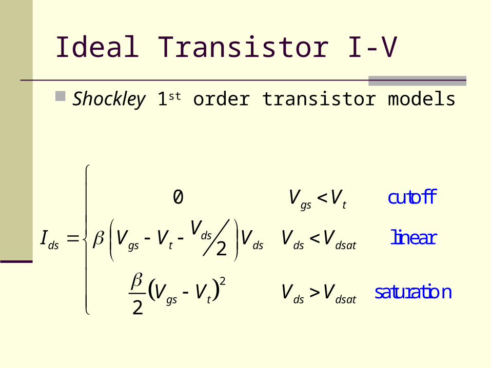
Ideal Transistor I-V
Shockley 1st order transistor models
2
cutoff
linear
saturatio
0
2
2n
gs t
dsds gs t ds ds dsat
gs t ds dsat
V V
VI V V V V V
V V V V
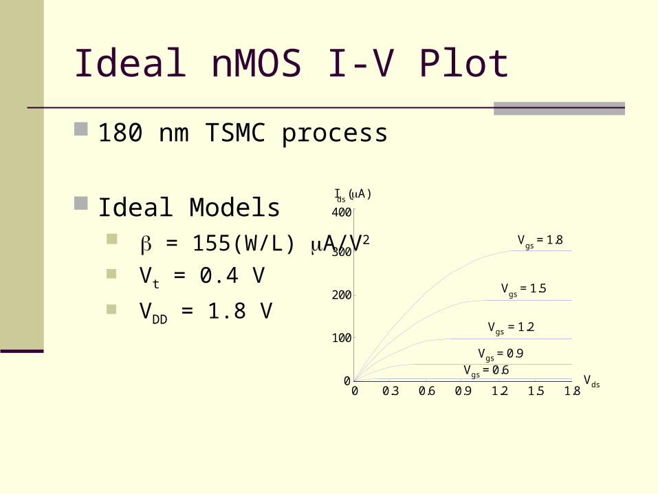
Ideal nMOS I-V Plot
180 nm TSMC process
Ideal Models = 155(W/L) A/V2
Vt = 0.4 V
VDD = 1.8 V
Ids
(A)
Vds0 0.3 0.6 0.9 1.2 1.5 1.8
100
200
300
400
Vgs = 0.6Vgs = 0.9
Vgs = 1.2
Vgs
= 1.5
Vgs
= 1.8
0

Simulated nMOS I-V Plot
180 nm TSMC process BSIM 3v3 SPICE models What differs?
Vds
0 0.3 0.6 0.9 1.2 1.5
Vgs = 1.8
Ids
(A)
0
50
100
150
200
250
Vgs
= 1.5
Vgs
= 1.2
Vgs
= 0.9
Vgs
= 0.6

Simulated nMOS I-V Plot
180 nm TSMC process BSIM 3v3 SPICE models What differs?
Less ON current No square law Current increases
in saturation
Vds
0 0.3 0.6 0.9 1.2 1.5
Vgs = 1.8
Ids
(A)
0
50
100
150
200
250
Vgs
= 1.5
Vgs
= 1.2
Vgs
= 0.9
Vgs
= 0.6
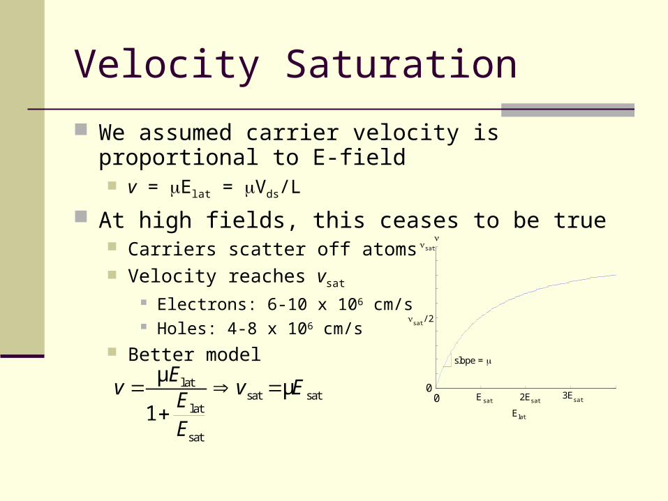
Velocity Saturation
We assumed carrier velocity is proportional to E-field v = Elat = Vds/L
At high fields, this ceases to be true Carriers scatter off atoms Velocity reaches vsat
Electrons: 6-10 x 106 cm/s Holes: 4-8 x 106 cm/s
Better model
Esat00
slope =
Elat
2Esat3E
sat
sat
sat
/ 2
latsat sat
lat
sat
μμ
1
Ev v E
EE
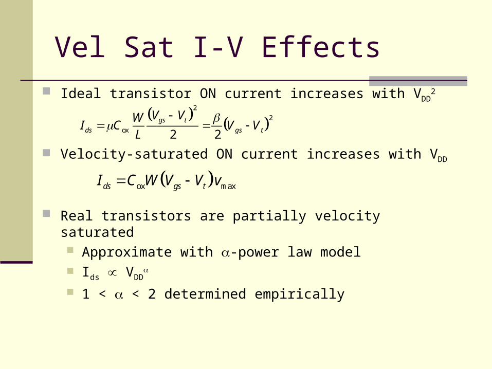
Vel Sat I-V Effects Ideal transistor ON current increases with VDD
2
Velocity-saturated ON current increases with VDD
Real transistors are partially velocity saturated Approximate with -power law model Ids VDD
1 < < 2 determined empirically
2
2
ox 2 2gs t
ds gs t
V VWI C V V
L
ox maxds gs tI C W V V v
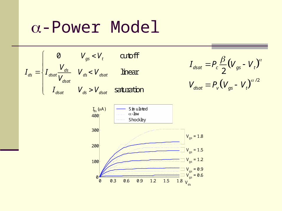
-Power Model
Ids
(A)
Vds
0 0.3 0.6 0.9 1.2 1.5 1.8
100
200
300
400
Vgs
= 0.6V
gs = 0.9
Vgs
= 1.2
Vgs
= 1.5
Vgs = 1.8
0
-lawSimulated
Shockley
0 cutoff
linear
saturation
gs t
dsds dsat ds dsat
dsat
dsat ds dsat
V V
VI I V V
V
I V V
/ 2
2dsat c gs t
dsat v gs t
I P V V
V P V V
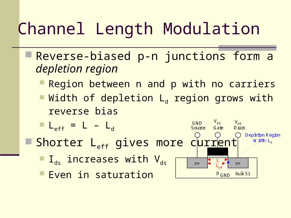
Channel Length Modulation
Reverse-biased p-n junctions form a depletion region Region between n and p with no carriers Width of depletion Ld region grows with reverse bias
Leff = L – Ld
Shorter Leff gives more current Ids increases with Vds
Even in saturation n+
p
GateSource Drain
bulk Si
n+
VDDGND VDD
GND
LL
eff
Depletion RegionWidth: Ld
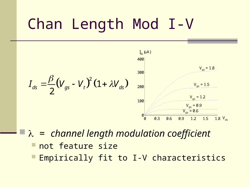
Chan Length Mod I-V
= channel length modulation coefficient not feature size Empirically fit to I-V characteristics
21
2ds gs t dsI V V V
Ids
(A)
Vds0 0.3 0.6 0.9 1.2 1.5 1.8
100
200
300
400
Vgs = 0.6Vgs = 0.9
Vgs
= 1.2
Vgs = 1.5
Vgs = 1.8
0
Body Effect
Vt: gate voltage necessary to invert channel Increases if source voltage increases
because source is connected to the channel Increase in Vt with Vs is called the body effect

Body Effect Model
s = surface potential at threshold
Depends on doping level NA
And intrinsic carrier concentration ni
= body effect coefficient
0t t s sb sV V V
2 ln As T
i
Nv
n
sioxsi
ox ox
2q2q A
A
NtN
C
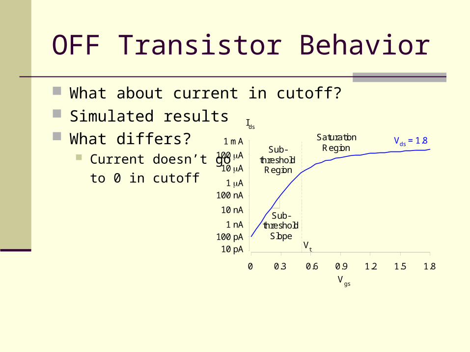
OFF Transistor Behavior
What about current in cutoff? Simulated results What differs?
Current doesn’t go
to 0 in cutoff
Vt
Sub-threshold
Slope
Sub-thresholdRegion
SaturationRegion
Vds = 1.8
Ids
Vgs
0 0.3 0.6 0.9 1.2 1.5 1.8
10 pA100 pA
1 nA
10 nA
100 nA1 A
10 A
100 A
1 mA
Leakage Sources
Subthreshold conduction Transistors can’t abruptly turn ON or OFF
Junction leakage Reverse-biased PN junction diode current
Gate leakage Tunneling through ultrathin gate dielectric
Subthreshold leakage is the biggest source in modern transistors
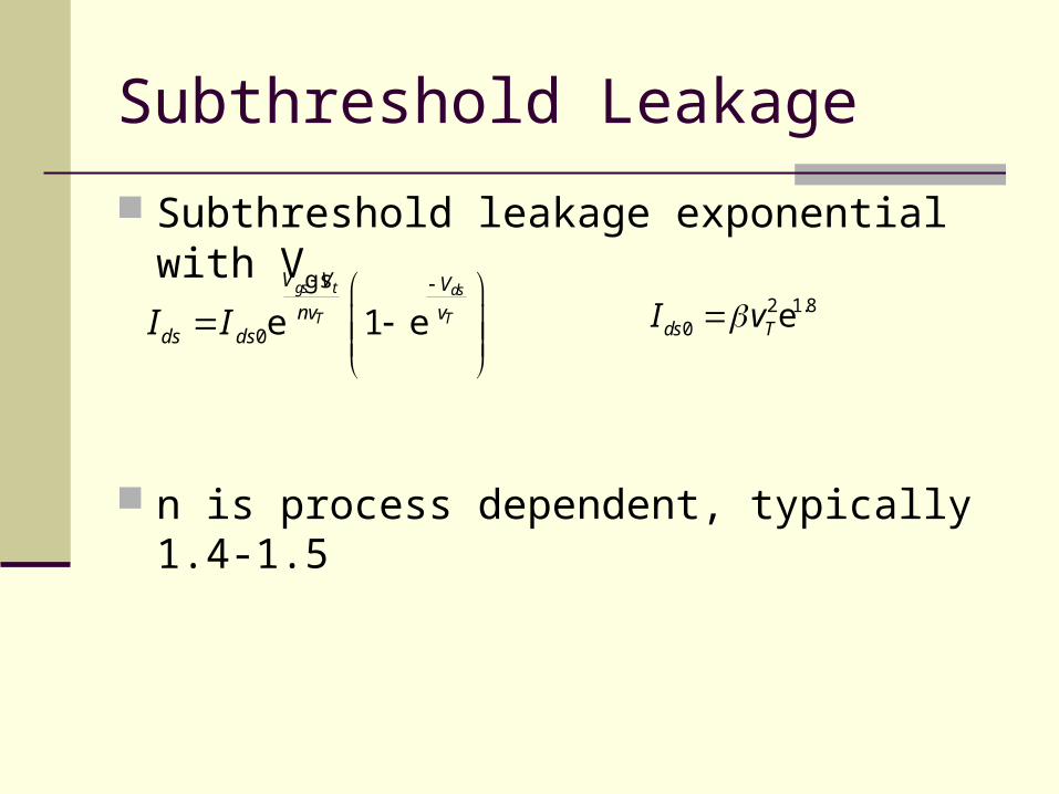
Subthreshold Leakage
Subthreshold leakage exponential with Vgs
n is process dependent, typically 1.4-1.5
0e 1 egs t ds
T T
V V V
nv vds dsI I
2 1.80 eds TI v
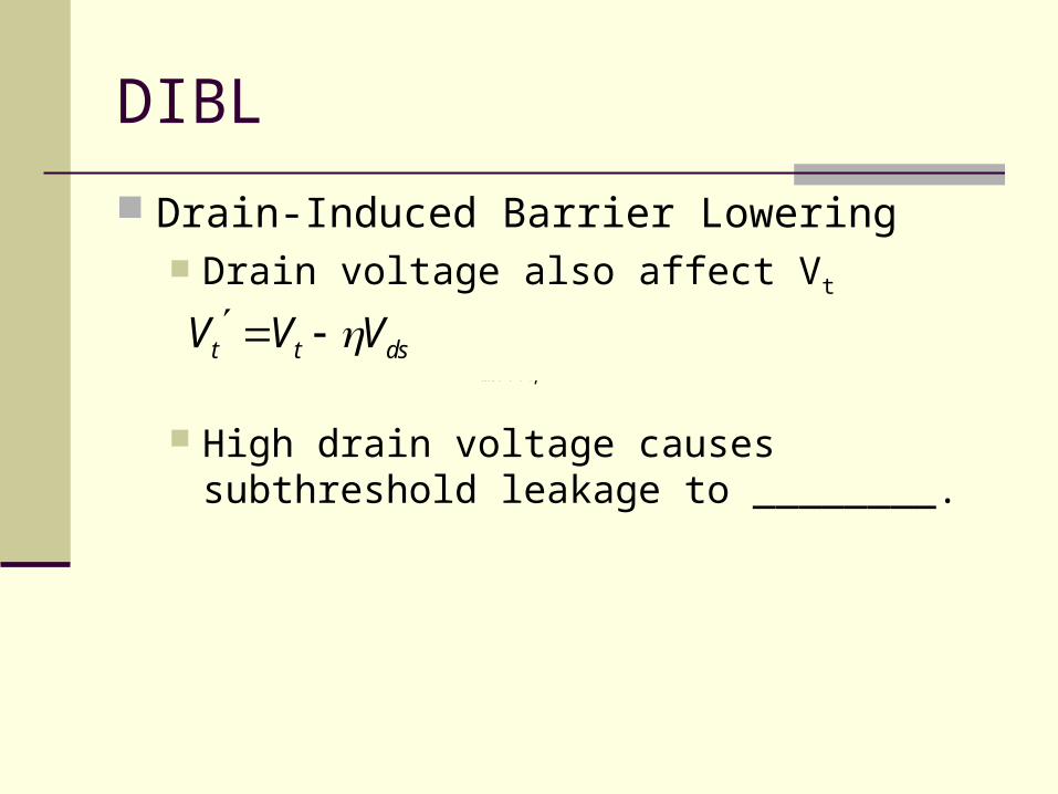
DIBL
Drain-Induced Barrier Lowering Drain voltage also affect Vt
High drain voltage causes subthreshold leakage to ________.
ttdsVVVt t dsV V V
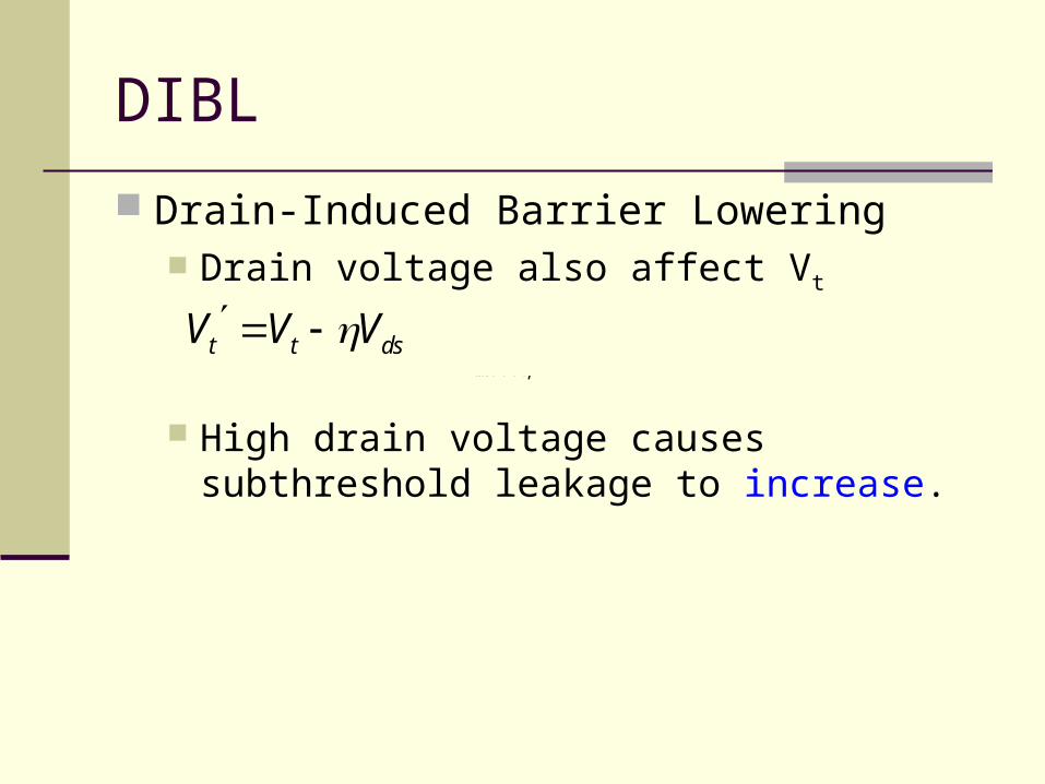
DIBL
Drain-Induced Barrier Lowering Drain voltage also affect Vt
High drain voltage causes subthreshold leakage to increase.
ttdsVVVt t dsV V V
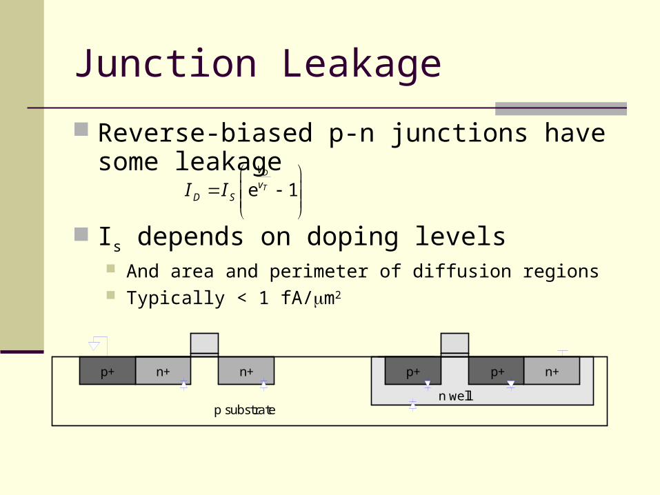
Junction Leakage
Reverse-biased p-n junctions have some leakage
Is depends on doping levels And area and perimeter of diffusion regions Typically < 1 fA/m2
e 1D
T
V
vD SI I
n well
n+n+ n+p+p+p+
p substrate
Gate Leakage
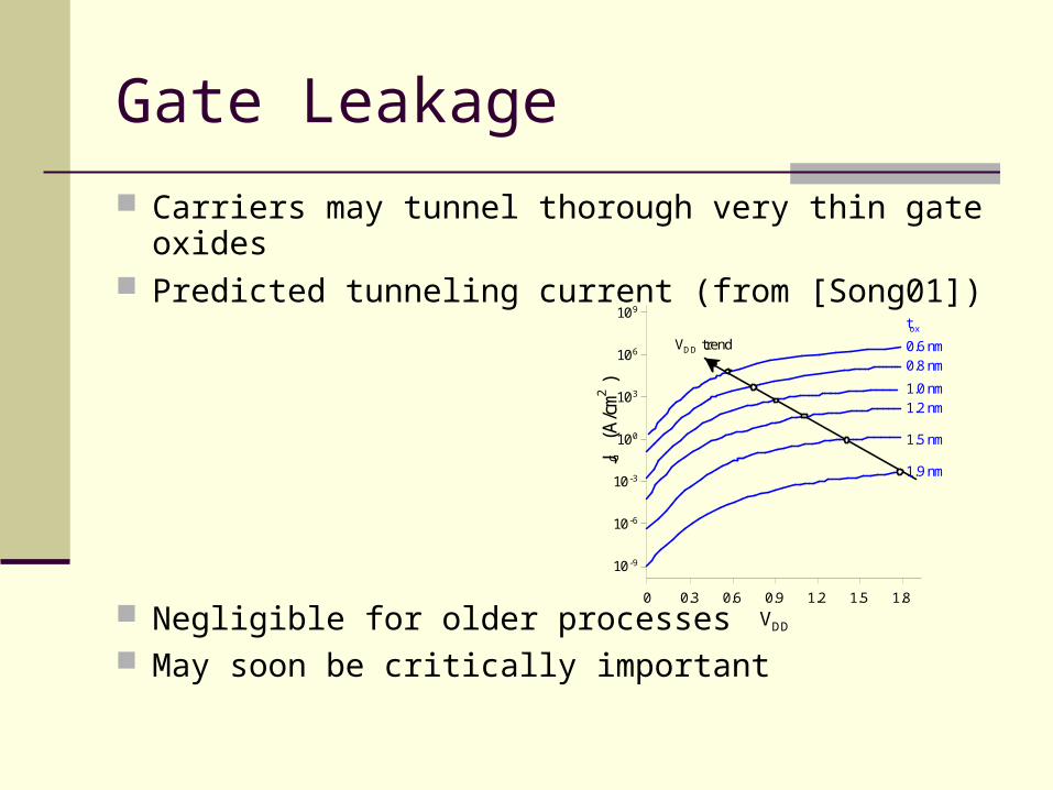
Carriers may tunnel thorough very thin gate oxides Predicted tunneling current (from [Song01])
Negligible for older processes May soon be critically important
VDD
0 0.3 0.6 0.9 1.2 1.5 1.8J G
(A
/cm2
)
10 -9
10 -6
10 -3
100
103
106
109
tox
0.6 nm0.8 nm
1.0 nm1.2 nm
1.5 nm
1.9 nm
VDD trend

Temperature Sensitivity
Increasing temperature Reduces mobility Reduces Vt
ION ___________ with temperature
IOFF ___________ with temperature

Temperature Sensitivity
Increasing temperature Reduces mobility Reduces Vt
ION decreases with temperature
IOFF increases with temperature
Vgs
dsI
increasingtemperature

So What?
So what if transistors are not ideal? They still behave like switches.
But these effects matter for… Supply voltage choice Logical effort Quiescent power consumption Pass transistors Temperature of operation
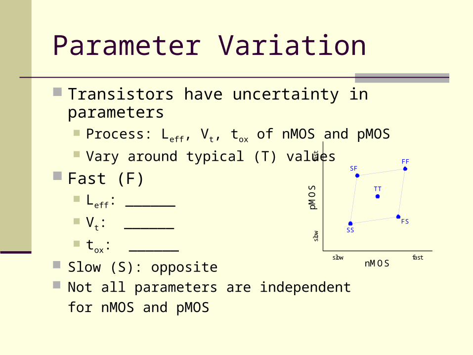
Parameter Variation
Transistors have uncertainty in parameters Process: Leff, Vt, tox of nMOS and pMOS Vary around typical (T) values
Fast (F) Leff: ______
Vt: ______
tox: ______
Slow (S): opposite Not all parameters are independent
for nMOS and pMOS
nMOS
pM
OS
fastslow
slow
fast
TT
FF
SSFS
SF

Parameter Variation
Transistors have uncertainty in parameters Process: Leff, Vt, tox of nMOS and pMOS
Vary around typical (T) values
Fast (F) Leff: short
Vt: low
tox: thin
Slow (S): opposite Not all parameters are independent
for nMOS and pMOS
nMOS
pM
OS
fastslow
slow
fast
TT
FF
SSFS
SF
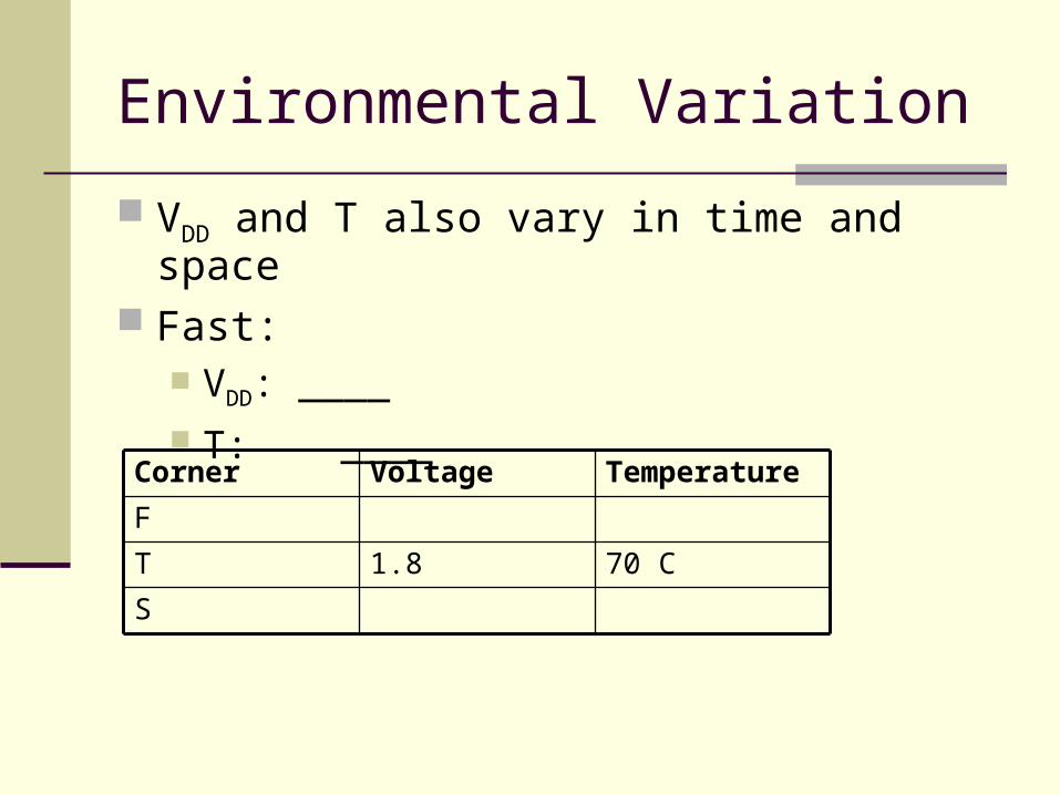
Environmental Variation
VDD and T also vary in time and space Fast:
VDD: ____ T: ____
70 C1.8T
S
F
TemperatureVoltageCorner
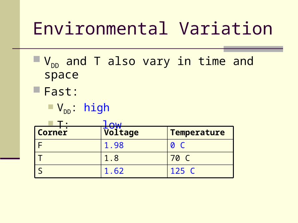
Environmental Variation
VDD and T also vary in time and space Fast:
VDD: high T: low
70 C1.8T
125 C1.62S
0 C1.98F
TemperatureVoltageCorner

Process Corners
Process corners describe worst case variations If a design works in all corners, it will probably
work for any variation.
Describe corner with four letters (T, F, S) nMOS speed pMOS speed Voltage Temperature

Important Corners
Some critical simulation corners include
Pseudo-nMOS
Subthrehold
leakage
Power
Cycle time
TempVDDpMOSnMOSPurpose
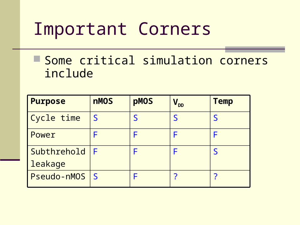
Important Corners
Some critical simulation corners include
??FSPseudo-nMOS
SFFFSubthrehold
leakage
FFFFPower
SSSSCycle time
TempVDDpMOSnMOSPurpose


