Voltage Sensing using MEMS Parallel-Plate Actuation Russell Y. Webb 1 , Noel C. MacDonald 2 1 Electrical and Computer Engineering, University of Canterbury, Christchurch, New Zealand [email protected]2 Department of Mechanical and Environmental Engineering, University of California, Santa Barbara, Santa Barbara, California, USA [email protected]Abstract Microelectromechanical systems (MEMS) have been proposed as DC electrical metrology references. The design reported here is the first to enhance the qualities of a MEMS DC reference with potential tuning and sensing via an isolated and monolithically integrated MEMS technology and, thereby, convert a stable parallel-plate voltage reference to a simple, sensitive, low-burden voltage sensor. This on-chip system reliably measures unknown potentials ranging from -60 V to 60 V with sampling times less than 10 msec. In the initial design, the system is used to measure atto-amp leakage current though 10 P!, suspended, MEMS isolation. Keywords: electrometer, pull-in, MEMS, parallel-plate, voltage reference, metrology, isolation 1 Introduction Quantitative electromechanical measurement of charge and potential was most famously demonstrated by Millikan [1] and simplified in later spring based systems [2]. In the literature, low temperature MEMS electrometers using resonance tuning caused by moving the input charge through a known external magnetic field have recently been demonstrated and studied [3]. General discussion of electrometer design including that of mechanical, spring-balanced electrometers can be found in older literature [4, 5]. Current proposals utilize the stability and precision of MEMS systems for DC and AC electrical metrology references [6, 7, 8]. For voltage sensing, the DC reference characteristics are most relevant. For voltages near 10 V, Rocha and Kärkkäinen found MEMS references based on parallel-plate pull-in can provide 500 μV accuracy, -1 mV/K temperature sensitivity [6], and voltage drift less than 100 μV/V per hour [7]. As is well known, an electrostatic parallel-plate actuator with a linear spring and an initial gap, g 0 , will pull-in (collapse) when actuated quasistatically at a critical voltage, V crit , where the gap has been reduced to 2/3 g 0 . A device combining such an actuator with a displacement or contact sensor and a means to vary the potential on one side of the actuator can be used to accurately measure an unknown potential on the other parallel-plate with minimal disruption of the system being measured. Parallel-plate pull-in time rather than voltage has been used for pressure sensing [9, 10], and one time use of pull-in coupled with stiction has been used for in situ potential measurement in plasmas [11]. In this paper, the following (Figure 1) single-crystal- silicon (SCS) MEMS electrometer is presented and analyzed as an example of on-chip potential sensing using parallel-plate pull-in to measure voltage. To our knowledge, this device is the first reported design to use pull-in as a voltage comparison technique for charge and potential measurement. An adjacent 45 deg mirror has been milled with a focused-ion-beam to provide means for in-plane vibrometer based confirmation of the device motion. Figure 1: On-chip electrometer 2 Pull-In Potential Sensing The pull-in voltage of parallel-plate actuators is used as voltage sensor by varying the potential on one side of the actuator and monitoring pull-in with an integrated or external sensor. Pull-in need not 1st International Conference on Sensing Technology November 21-23, 2005 Palmerston North, New Zealand 106
Transcript
Voltage Sensing using MEMS Parallel-Plate Actuation
Russell Y. Webb1, Noel C. MacDonald2
!1Electrical and Computer Engineering,!
University of Canterbury, Christchurch, New Zealand !
provided accurate, simple, and low burden sensing. A
micrograph of the device with integrated potential
sensing is shown in Figure 1; while, the circuit
corresponding to the measurement setup is shown in
Figure 5.
1st International Conference on Sensing TechnologyNovember 21-23, 2005 Palmerston North, New Zealand
107
Figure 5: On-chip electrometer circuit
The swept voltage used to vary the potential across the
actuator is Vin.
To use parallel-plate instability in a sensor application,
it is important to have a well-defined, stable closing
voltage. Fringing fields and spring non-linearities will
cause the instability point to differ from two thirds the
starting plate separation but will not impact it’s
usefulness as a sensor under the quasistatic actuation
used here. Device asymmetries arise mainly from the
use of bump-stops which cause fringing field
asymmetries, leading to each plate having a different
effective contribution to the potential across the
actuator. Defining the normal closing voltage, Vcrit, to
be the input voltage needed to close the actuator with
the voltage on the fixed plate being the same potential
as the wafer, the following formula relates the input
voltage, Vin, and reference voltage, Vfix, to the normal
closing voltage:
!
Vcrit =Vin "#Vfix , (1)
where ! represents the influence of Vfix relative to Vin.
Ideally !=1, but it is more important to determine its
value for a particular design by stepping Vfix and
measuring its effect on the closing voltage by
sweeping Vin. Such a sweep is shown below for the
extremely asymmetric design of Figure 1 for which
!=0.6345; further accuracy can be obtained by adding
a cubic term, but the correction provided by this term
is less than 1% for voltages between -20 V and 20 V.
Figure 6: Measured linearity
Particularly when using a probe station, measured Vcrit
can drift by up to 10mV per hour. This drift is likely
do to variations in probe contact resistance since after
the first hour the drift rate decreases to less than 2mV
per hour.
Once the parallel-plate actuator is closed the potential
across the actuator must be reduced to release the
plate. A large contact area can result in surface forces
capable of holding the actuator closed with no applied
voltage. To avoid this stiction, small protrusions
(called bump stops or simply stops) are used which
contact before the full plate area. These stops serve to
increase the minimum releasing voltage by reducing
surface interactions and increasing the minimum plate
separation which reduces the force between the plates
for a given voltage and minimize the current spike
caused by the capacitor’s collapse [14]. The simplest
design is to locate the stops on one side of the parallel-
plate. A better arrangement is to design a separate
stop, either grounded or electrically connected to the
moving plate. Because the moving plate will contact
this stop, the moving plate is usually used to carry the
known voltage leaving the unknown and possibly
sensitive potential isolated by an air-gap.
This sensor system needs to approach instability
quasistatically, so its maximum operating frequency
must be significantly below its natural frequency. The
cantilever based systems studied have a resonant
frequency of ~50 kHz and are capable of measuring
potentials with the range ±60 V with 5 mV precision
at a sampling rate of >30 Hz. Because the device is
tested in air, its Q is fairly low (around 20); coupled
with its high resonant frequency this means that the
system will effectively reach equilibrium in less than 2
msec at which point its energy will have damped to
.67% (1/e5) of the initial energy.
The dynamics of the closing and opening of a
threshold actuator are shown in Figure 7. The data was
collected using a commercial vibrometer after cutting
a 45 degree mirror (Figure 1) using a focused ion
beam. The recorded instability point is greater than
one half the total movement because the motion is
limited by a bump-stop (the designed gap between
actuator plates is 4 !m in this design).
Figure 7: Pull-in measured via vibrometry
RefCap Voltage [V]
Clo
sin
g V
olt
ag
e [
V]
Time [sec]
Dis
tan
ce [
µm
]
1st International Conference on Sensing TechnologyNovember 21-23, 2005 Palmerston North, New Zealand
108
4 Operation and Results
The sensor in Figure 5 has several unknown
characteristics which much be determined before
calibrated measurements can be made:
a. Vcrit, the normal pull-in potential of actuator.
b. !, the relative effectiveness of Vfix on the
potential difference.
c. Cfix, the capacitance of the reference.
d. Rfix, the parasitic resistance of the reference.
Vcrit is determined by setting Vfix = 0 and sweeping Vin
until pull-in occurs. ! is determined as described in
Section 3. Since Cfix is fairly large for this application,
it is measured with a commercial LCR meter (HP-
4274A). Rfix is difficult to measure because the
capacitor is a MOS structure with a thermal oxide
guard ring minimizing leakage. Conveniently, Rfix is
the last unknown in an electrometer design so the
device itself can be used to measure Rfix serving as a
demonstration of the device’s usefulness. Once Rfix is
known, small currents applied to Cfix from other
sources can be measured by the voltage change at Vfix.
The procedure for determining Rfix is defined below:
1. Determine Vcrit, !, and Cfix.
2. Apply a known potential, Vknown, to Vfix.
3. Begin recording the Vfix needed to satisfy
equation (1) by sweeping Vin.
4. Remove the known potential from Vfix and
allow Cfix to self-discharge through Rfix.
Using the determined values of Vcrit=39.293 V (note
accurate knowledge of Vcrit is never used), !=0.6345,
and Cfix=2.98 pF, the measured change in Vfix is
graphed in Figure 8 when Vknown = 20 V.
Figure 8 : Discharge of Cfix
By comparing the closing voltage to the known
relationship between capacitor voltage and closing
voltage, the corresponding capacitor voltage is
determined. Comparing this voltage with a pervious
measurement is used to determine the average current
between the measurements:
!
R =Vavg
Iavg=Vavg (t2 " t1)
C#V
Figure 9: Measured parasitic resistance, Rfix
From this analysis, the parasitic resistance of our
charge accumulation capacitor is found to be greater
than 1.5 P" for voltages below 20 V allowing the
system to directly measure averaged currents in the
atto-amp range.
Smaller input currents can be measured if Rfix is
included in the charging model. To illustrate this
process, a charging current was generated by applying
voltage, Viso = 100 V, to a single suspended MEMS
isolation of resistance Riso. The charging equation for
such a system is
!
Vfix =VisoRfix
Riso + Rfix
1" e
" t
C fix
1
Riso+1
R fix
#
$ % %
&
' ( (
#
$
% %
&
'
( (
.
The measured 1700 data points and Mathematica
curve fit with residuals always below 1 V are shown
below. The system charges slightly faster in the
beginning than predicted by the model which is due to
the higher parasitic resistance in the capacitor at small
voltages (as can be seen in Figure 9) not represented
in the model. The curve fit puts both Riso and Rfix
within 2% of 10 P".
Figure 10: Charging via atto-amp current
The fit indicates an internal resistance of 10 P" for
the capacitor, comparable to the value measured by
Time [sec]
Time [sec]
Voltage [V]
Vo
ltag
e [
V]
Cap
acit
or
Vo
ltag
e [
V]
Resi
stan
ce [
Oh
ms]
1st International Conference on Sensing TechnologyNovember 21-23, 2005 Palmerston North, New Zealand
109
monitoring the capacitor discharge directly. Taking
this value as a reasonable approximation and
presumably an accurate value for some voltage
between 0 and 50 V, the resistance of the isolation
segment can be evaluated, using the same incremental
method used above to determine the guarded anchor
resistance, by adding the current drained away by the
internal leakage of the capacitor to the measured
current since the isolation leakage is also supplying
current to make up for the self-discharge of the
capacitor. The result of this analysis is shown Figure
11 with error bands and indicates that a resistance of
10 P" is reasonable.
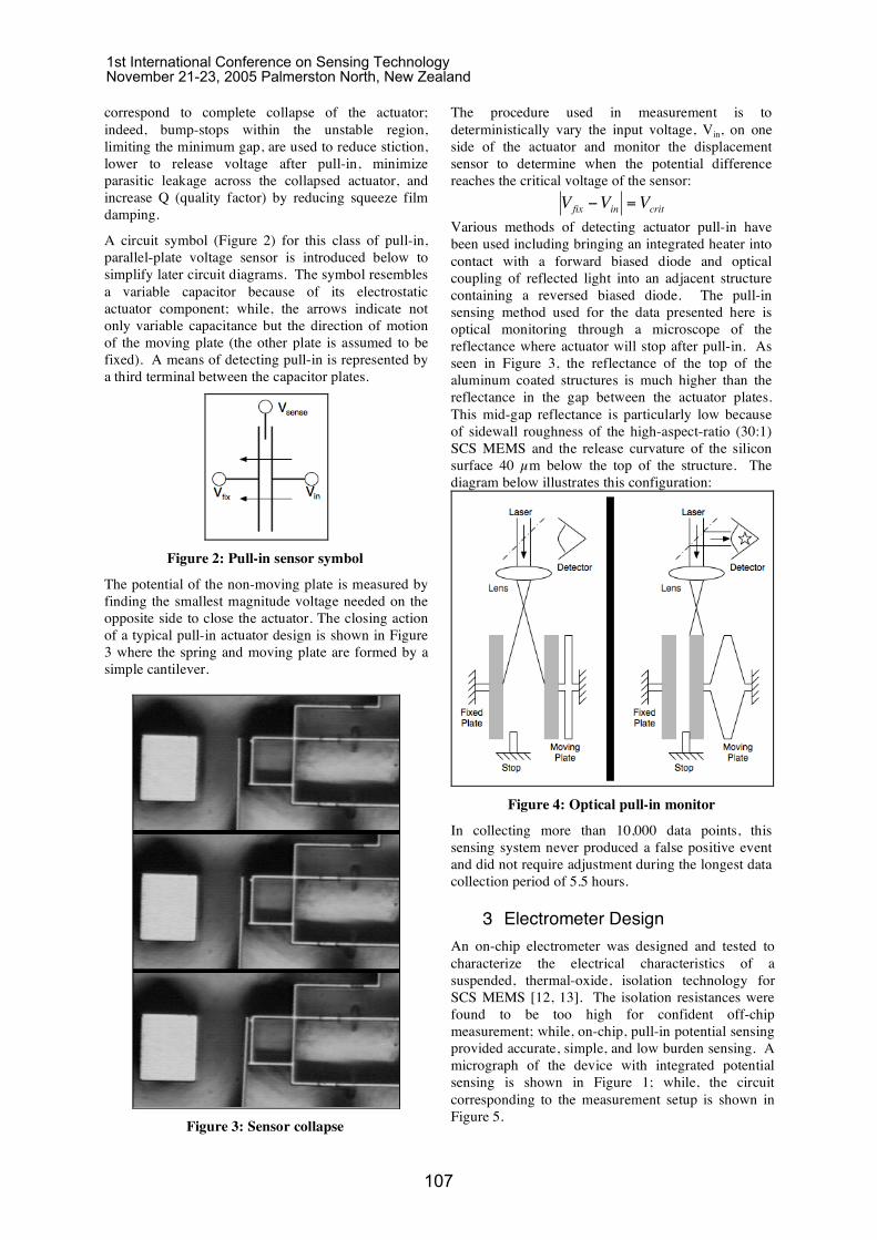
Figure 11: Incremental isolation resistance
As described in Sze [15], the conduction, in steady-
state, through oxide at low field strength (i.e. far from
breakdown) is ohmic, essentially independent of oxide
thickness for a given field strength, and results from
thermally excited electrons hopping between isolated
states. For this 2 µm thick oxide isolation with an area
of 20 µm2 to have a 10 P" resistance, the oxide
resistivity is approximately 1013 "cm which falls in
the range of measured for bulk oxide in the literature
[16].
5 Conclusion and Extensions
This system is distinguished by its simplicity, atto-
amp sensitivity, P" isolation up to 20 V, and large
voltage-sensing range. Sensing fA currents with P"
input resistances is typical of relatively modern
electrometers [17]. Unlike other configurations, since
an air-gap is maintained between the sensing actuator
and charge integrating capacitor, the sensor burden is
relatively independent of sensing frequency.
Since this sensing system is monolithically integrated
with a commercial grade MEMS technology (used in
commercial production at Kionix, Inc. and Calient
networks) with microfluidic capabilities [18], it opens
many avenues for future investigation including:
a. Sensors for level triggering by biasing a
sensor near pull-in.
b. Differential on-chip MEMS actuators and
accelerometers applied to motion
transduction.
c. Further exploration of on-chip sensing
methods.
d. Low temperature detection of ultra-small
charges.
e. Dynamics studies using shaped pulses to
maximize sampling frequency.
f. Integration with on-chip relays for capacitive
discharge allowing self-contained calibrated
potential measurement.
6 Acknowledgements
Many graduate students in the MEMS group at
Cornell University have helped, directly and
indirectly, to achieve the result reported here. This
work was done at the Cornell Nanofabrication Facility
whose staff makes so much research possible. Funding
for this project was provided by DARPA.
7 References
[1] Millikan, R.A., “The Isolation of an Ion, a Precision measurement of its Charge, and the Correction of Stoke’s Law”, The Physical
Review, vol. 22, no. 4, pp. 349-397, April 1911.
[2] Yousef, Y.L., Kamel, R., “A vibrating needle electrometer”, Journal of Scientific Instruments,
vol. 31, pp. 13-15, January (1954).
[3] Cleland, A.N., Roukes, M.L., “A nanometer-scale mechanical electrometer”, Nature, vol. 392, pp. 160-162, 12 March (1998).
[4] Hansen, W. W., “On the General Theory of
Electrometer Design”, Review of Scientific
Instruments, vol. 7, pp. 182-191, April (1936).
[5] Palevsky, H., Swank, R. K., Grenchik, R.,
"Design of Dynamic Condenser Electrometers",
The Review of Scientific Instruments, vol. 18,
no. 5, pp. 298 - 314, May (1947).
[6] Rocha, L.A., Cretu, E., Wolffenbuttel, R.F.,
“Stability of a Micromechanical Pull-In Voltage Reference”, IEEE Transactions on Instrumentation and Measurement, vol. 52. no.
2, pp. 457-460, April (2003).
[7] A. Kärkkäinen, S.A. Awan, A.Oja, J.
Kyynäräinen, A. Manninen, N. Tisnek and H. Seppä, ”Optimized Design and Process for Making a DC Voltage Reference Based on MEMS”, Accepted for publication in the CPEM
2004 Special issue of the IEEE Trans I&M.
[8] A. Kärkkäinen, N. Pesonen, M. Suhonen, J.
Kyynäräinen, A.Oja, A. Manninen*, N. Tisnek* and H.Seppä, “Towards MEMS Based Electrical Metrology”, XXXIV Fysiikan päivät, 17-
19.3.2005, Espoo, Finland.
[9] Gupta, R. K., Hung, E. S., Yang, Y. J.,
Ananthasuresh, G. K., Senturia, S. D., " Pull-In
Voltage on Isolation [V]
Resi
stan
ce [
Oh
ms]
1st International Conference on Sensing TechnologyNovember 21-23, 2005 Palmerston North, New Zealand
110
Dynamics of Electrostatically-Actuated Beams",
Proceedings of the 1996 Solid-State Sensor and
Actuator Workshop, Late News Session, pp. 1 -
2, June 3 - 6, (1996).
[10] Gupta, R. K., Senturia, S. D., "Pull-In Time
Dynamics as a Measure of Absolute Pressure",
Tenth Annual International Workshop on Micro
Electro Mechanical Systems, MEMS 1997, pp.
290 - 294, January 26 - 30, (1997).
[11] Pangal, K., Firebaugh, S. L., Sturm, J. C.,
"Noninvasive measurement of charging in
plasmas using microelectromechanical charge
sensing devices", Applied Physics Letters, vol.
69, no. 10, pp. 1471 - 1473, September 2, (1996).
[12] Webb, R. Y., Adams, S. G., MacDonald, N. C.,
"Suspended Thermal Oxide Trench Isolation for
SCS MEMS", Proceedings of the SPIE - The
International Society for Optical Engineering,
Microrobotics and Micromanipulation, vol. 3519,
pp. 196-199, November 4 - 5 (1998).
[13] Webb, R. Y., "Suspended Thermal Oxide
Isolation for Actuation and Small Current
Measurement in MEMS", Ph.D. Dissertation, Cornell
University, (2000).
[14] Castaner, L. M., Senturia, S. D., “Speed-Energy
Optimization of Electrostatic Actuators Based on
Pull-In”, IEEE Journal of Microelectromech-
anical Systems, vol. 8, no. 3, pp. 290-297,
September (1999).
[15] Sze, S. M., “Current Transport and Maximum
Dielectric Strength of Silicon Nitride Film”, Journal of Applied Physics, vol. 38, no. 7, pp.
2951-2956, June (1967).
[16] Johansen, I. T., “Electrical Conductivity in Evaporated Silicon Oxide Film”, Journal of Applied Physics, vol. 37, no. 2, pp. 499-507,
February (1966).
[17] Cover, K. S., “Construction of a Prototype MOS
Electrometer”, Review of Scientific Instruments,
vol. 60, no. 8, pp. 2733 - 2739, August (1989).
[18] Chong, J. M., "Suspended Channels and Channel
Actuators for Microfluidic Applications", Ph.D.
Dissertation, Cornell University, (2000).
1st International Conference on Sensing TechnologyNovember 21-23, 2005 Palmerston North, New Zealand