Visit analogdialogue.com Performance Optimization of Multichannel Data Acquisition (DAQ) Systems: The Untold Story of the Input Settling Time Moving Up the Stack Challenges for Measurement Engineering at ADI The Refulator: The Capabilities of a 200 mA Precision Voltage Reference iCoupler Isolated Communication Solutions for Essential Monitoring of Solar PV and Energy Storage An Integrated Bidirectional Bridge with Dual RMS Detectors for Return-Loss and VSWR Measurement High Speed Amplifier Testing Involves Enough Math to Make Your Balun Spin! Isolated Gate Drivers—What, Why, and How? LED Driver for High Power Machine Vision Flash 5 10 14 23 27 44 48 52 34 Single, 2 MHz Buck-Boost Controller Drives Entire LED Headlight Cluster Meets CISPR 25 Class 5 EMI Volume 52, Number 2, 2018 Your Engineering Resource for Innovative Design
Transcript
Visit analogdialogue.com
Performance Optimization of Multichannel Data Acquisition (DAQ) Systems: The Untold Story of the Input Settling Time
Moving Up the Stack Challenges for Measurement Engineering at ADI
The Refulator: The Capabilities of a 200 mA Precision Voltage Reference
iCoupler Isolated Communication Solutions for Essential Monitoring of Solar PV and Energy Storage
An Integrated Bidirectional Bridge with Dual RMS Detectors for Return-Loss and VSWR Measurement
High Speed Amplifier Testing Involves Enough Math to Make Your Balun Spin!
Isolated Gate Drivers—What, Why, and How?
LED Driver for High Power Machine Vision Flash
5
10
14
23
27
44
48
52
34 Single, 2 MHz Buck-Boost Controller Drives Entire LED Headlight Cluster Meets CISPR 25 Class 5 EMI
Volume 52, Number 2, 2018 Your Engineering Resource for Innovative Design
Performance Optimization of Multichannel Data Acquisition (DAQ) Systems: The Untold Story of the Input Settling TimeFind out how settling transients at the inputs of the multiplexer, caused by a large scale switching transient at the multiplexer output, requires prolonged acquisition time, effectively decreasing the overall throughput of the multichannel data acquisition system. An untold story about the input settling time.
5
Moving Up the Stack Challenges for Measurement Engineering at ADIHave you thought about the difficulties that test floor measurement engineers face when measuring chip accuracy? When I was a student, the rule was a measurement system needed to be at least 10× better than the device itself—a challenge to achieve nowadays.
10
The Refulator: The Capabilities of a 200 mA Precision Voltage ReferenceReferences have, in many cases, one huge disadvantage: you are not able—or your ability is very limited—to get current out of a reference. If you need a precise voltage but just a bit of a current, then you require an external LDO with external components and space on the PCB. The refulator offers a solution.
14
Rarely Asked Questions—Issue 152: Problem Solver: Multiplying Digital-to-Analog ConverterYou probably know that some DACs contain an R2R network to generate a voltage reference at the output. Those Rs are precise resistors. They are normally used to switch the current based on the digital value sent to the DAC to create a voltage at the output amplifier. With multiplying DACs, the output amplifier is not integrated. This offers an opportunity for unusual applications and using the R2R network as a resistor.
21
iCoupler Isolated Communication Solutions for Essential Monitoring of Solar PV and Energy Storage Even for a private solar installation, communication with dc-to-dc converter(s), house battery, or backup-power among different system components is essential for an optimized system. This article discuss how iCoupler® technology can be used not only in isolated gate drivers for IGBTs, but also in isolated RS-485 communication chips to improve safety and security.
23
Analog Dialogue Volume 52 Number 2 3
An Integrated Bidirectional Bridge with Dual RMS Detectors for Return-Loss and VSWR MeasurementThis article from Eberhard Brunner and Eamon Nash addresses the RF market and introduces a new chip concept. The ADL5920 is an integrated bidirectional bridge with dual rms detectors. Its tiny size allows a drop-in for many applications.
27
Single, 2 MHz Buck-Boost Controller Drives Entire LED Headlight Cluster Meets CISPR 25 Class 5 EMI Our next article addresses a new IC challenge as well. When I owned a VW Beetle many years ago, the only lights were the headlights, brake lights, and blinkers. All individual lamps were traditional Wolfram-based lamps. Today, LEDs have taken over. High beams, low beams, daytime lights, clearance lights, different signal lights, and fancy blinkers are all implemented with LEDs. Ever thought about what it takes to power all those LED clusters?
34
Rarely Asked Questions—Issue 153: High Speed ADC Power Supply DomainsIn our RAQ, Thomas Tzscheetzsch discusses the use of the disable pin of an amplifier. This could dramatically reduce the power requirements in a battery-powered IoT system. The question remaining—does it impact the performance of a design?
40
High Speed Amplifier Testing Involves Enough Math to Make Your Balun Spin!The article is about high speed amplifier testing. Certainly math is involved, but why does a balun spin? Rob Reeder’s article adds a bit of humor, using Balun as a play on words in the title.
44
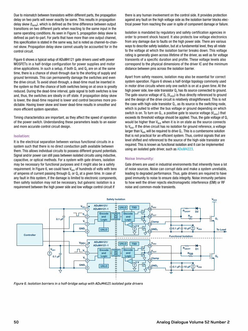
Isolated Gate Drivers—What, Why, and How? You know that an IGBT/MOSFET is a voltage-controlled device that is used as a switching element in power supply circuits and motor drives amongst other systems. The gate is the electrically isolated control terminal for each device. The other terminals of a MOSFET are source and drain, and for an IGBT they are called collector and emitter. So how do you now drive an MOSFET/IGBT? This article will explain
48
Analog Dialogue Volume 52 Number 24
In This Issue
LED Driver for High Power Machine Vision Flash When you need a very fast flash light for your high speed camera inspection system, you know how hard it can be to create that very high current in a very short time (µsec), and over a long period. Creating short and square LED flash waveforms separated by long periods (100 ms to 1 s) of time is not trivial.
52
Rarely Asked Questions—Issue 154: Pocket-Size White Noise Generator for Quickly Testing Circuit Signal Response Do you need a signal with all frequencies present at the same moment in time? A frequency spectrum with no missing frequency? Yes? Why not use a white noise generator with an op amp to do this job? A white noise generator produces all frequencies at the same time.
55
Analog Dialogue is a technical magazine created and
published by Analog Devices. It provides in-depth design
related information on products, applications, technology,
software, and system solutions for analog, digital, and
mixed-signal processing. Published continuously for over
50 years—starting in 1967—it is produced as a monthly
online edition and as a printable quarterly journal featuring
article collections. For history buffs, the Analog Dialogue
archive includes all issues, starting with Volume 1, Number 1,
and four special anniversary editions. To access articles,
the archive, the journal, design resources, and to subscribe,
visit the Analog Dialogue homepage, analogdialogue.com.
Bernhard Siegel, Editor Bernhard became editor of Analog Dialogue in March 2017, when the preceding editor, Jim Surber, decided to retire. Bernhard has been with Analog Devices for over 25 years, starting at the ADI
Munich office in Germany.
Bernhard has worked in various engineering roles including sales, field applications, and product engineering, as well as in technical support and marketing roles.
Residing near Munich, Germany, Bernhard enjoys spending time with his family and playing trombone and euphonium in both a brass band and a symphony orchestra.
ADCs are the most commonly used type of ADC for these applications due to their combination of speed and precision.
High channel density precision DAQ systems for industrial and medical applications aim to compress the largest number of channels into the least possible area. Multiplexed DAQ systems, generally, can achieve high density, high throughput, and good energy efficiency by:
1. Using a high speed precision SAR ADC
2. Using the minimum sampling rate per channel
3. Maximizing the SAR ADC converter utilization where:
SAR ADCConverter Utilization
× 100%n × Sampling Rate Per Channel
SAD ADC Sampling Rate= (1)
with n as the number of channels. The overall throughput of the multichannel data acquisition system, per converter, is given by:
OverallThroughout
(SAR ADC Converter Utilization× SAR ADC Sampling Rate)× Resolution
= (2)
This shows that the overall throughput of the multichannel DAQ system is not only dependent on the speed and resolution of the SAR ADC, but also on how well this converter is utilized.
AbstractIn a multichannel, multiplexed data acquisition system, increasing the number of channels per ADC improves the system’s overall cost, area, and power efficiency. The high throughput and energy efficiency of modern, successive approximation register analog-to-digital converters (SAR ADCs) allow system designers to achieve greater channel density than ever before. This article will describe how settling transients at the inputs of the multiplexer, caused by a large scale switching transient at the multiplexer output, requires prolonged acquisition time, effectively decreasing the overall throughput of the multichannel data acquisition system. It will then focus on design trade-offs when minimizing the input settling time, and improving data throughput and system efficiency.
What Is a Multichannel DAQ and How Do We Measure the Performance of a Multichannel DAQ?A multichannel data acquisition (DAQ) system is a complete signal chain subsystem interfaced to multiple inputs (typically sensors) with the main function of converting the analog signal at the inputs into digital data that a processing unit can comprehend. The main components of a multichannel DAQ system are the analog front-end subsystem (a buffer, a switching ele-ment, and signal conditioning block), the analog-to-digital converter (ADC), and the digital interface. For high speed, precision converters, the switch-ing element (typically a multiplexer) is placed before the ADC driver and the converter itself to exploit the advancing performance of modern ADCs. SAR
Performance Optimization of Multichannel Data Acquisition (DAQ) Systems: The Untold Story of the Input Settling TimeBy Joseph Leandro Peje
MuxFilter and
SignalConditioning
SARADC
Inte
rfac
e
Figure 1. A typical SAR ADC-based, multiplexed data acquisition system block diagram.
How Do Delays Affect the Performance of Multichannel DAQ Systems?In the presence of any settling delays, a term td is added to the actual sampling and conversion period of the ADC, leading to an actual maximum converter sampling rate given by:
SRADC, actual, max = TADC + td 1 Sample
(3)
wherein TADC is the ADC period per sample (typically found in most ADC data sheets and more commonly the inverse of the SAR ADC sampling rate in seconds per sample). The actual maximum sampling rate of the multichannel DAQ system is always less than the sampling rate of the converter for a non-zero delay td, resulting in a converter utilization that is always less than 100%. From this we can see that any delay that is added to the sampling and conversion period reduces converter utilization. When related to an earlier expression for overall throughput, this effectively reduces the maximum number of channels the multichannel DAQ can accommodate. To summarize, any settling delays decrease the channel density and/or the overall throughput of the multichannel DAQ system.
Now, What Is the Multiplexer Input Switching Glitch and Input Settling Time?When a multiplexer switches from one input to another, the output still has a memory of the previous input channel in the form of stored charges in the output load capacitance and the parasitic drain capacitance of the multiplexer. This is more evident for highly capacitive loads such as ADC drivers and the ADCs themselves, since there is no low impedance path these stored charges can go. You can even say that these charges are trapped due to the capacitive nature of the output and high impedance of the multiplexer due to the break-before-make (BBM) mechanism of modern multiplexers; they can only be discharged once switched to the next input.
VA
VB
CA
CB
COUT
VOUT = VBΔVC
VA – ΔV
VB
CA
CB
COUT
VOUT = VA – ΔV
Figure 2. The preswitching state is shown on the left. After switching, charge sharing happens, which causes a quick voltage drop ∆V (right).
After switching, the input capacitance CA will be connected in parallel to the output capacitance COUT. CA and COUT, however, may initially be at different potentials, which will cause charge sharing between CA and COUT. The charge sharing happens almost instantaneously for very high bandwidth multiplexers, causing a high frequency glitch in the input of the multiplexer. The magnitude of this glitch, ΔV, is given by:
∆V = ∆VC + 1
CACOUT
1(4)
where ΔVC is the difference in capacitor voltages before switching. The transient glitch happening at the input side of the multiplexer is a phenomenon more commonly known as the kickback and is more prevalent for switched applications with highly capacitive loads such as ADCs, capacitive DACs, and sampling circuits to name a few. This subject is briefly illustrated in MT-088. The glitch will have to settle to within 1 LSB of the output to produce valid data for the converter and the time it takes for the input to settle to within 1 LSB (and stay in that range!) is the input settling time (tS). tS is a component of the delay td described earlier, and it may have the most significant contribution to this term.
When ADCs weren’t as fast as they are today, these glitches and their respective input settling time were insignificant enough to be ignored. However, as ADCs scale their speed, the converter sampling period becomes shorter and shorter, approaching the order of the input settling time. As described earlier, when the ADC period, TADC, is equal to the input settling time tS (and effectively td), the converter utilization is greatly reduced to 50%. This means we’re using only half of what the converter is capable of! Reiterating its significance, the input settling time should start scaling with the speed of the current technology of precision converters, paving the way to advance the performance of multichannel DAQ systems.
How Do We Minimize Input Settling Time?The switching glitches are usually minimized by using an RC filter between the buffer amplifier and the multiplexer (see CN-0292), known as a snubber network. A signal chain subsystem for a 2-channel, multiplexed analog front-end subsystem and its corresponding switching timing diagram is described in Figure 3.
OPA
OPB
VIN, A
VA
VOUT VIN, A
VA
VIN, A
VIN, B
VIN, A
VIN, BVOUT
SEL
Input
Input GlitchS1
S0
VIN, B
SEL
Figure 3. A 2-channel multiplexed analog front-end subsystem for a multichannel DAQ system and the corresponding timing diagram.
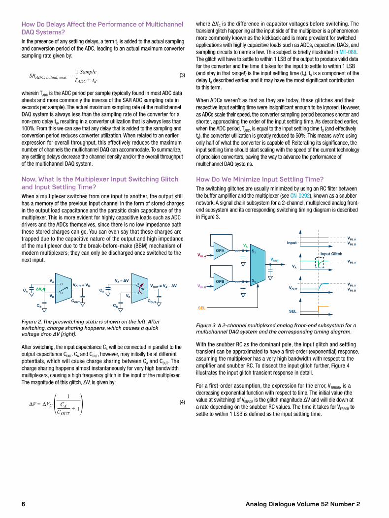
With the snubber RC as the dominant pole, the input glitch and settling transient can be approximated to have a first-order (exponential) response, assuming the multiplexer has a very high bandwidth with respect to the amplifier and snubber RC. To dissect the input glitch further, Figure 4 illustrates the input glitch transient response in detail.
For a first-order assumption, the expression for the error, VERROR, is a decreasing exponential function with respect to time. The initial value (the value at switching) of VERROR is the glitch magnitude ΔV and will die down at a rate depending on the snubber RC values. The time it takes for VERROR to settle to within 1 LSB is defined as the input settling time.
The converter, on the other hand, samples at a period tACQ (also called the acquisition time). At the ADC conversion phase when tACQ elapses, the converter will quantize whatever sampled data is available. This will be problematic if VERROR died down too slow and did not settle to within a certain value (1 LSB to a few LSBs). This will cause the current sample to be corrupted by the previous analog input and resulting in cross-talk between the ADC channels. With the input settling time in mind, it is imperative to assure that the input settling time is less than the converter acquisition time to minimize errors. Moreover, further minimizing tS opens up an opportunity to use faster converters to improve the overall throughput and density of the system.
With some math in our repertoire, the expression for the fastest input settling time can be derived at worst case when ΔVC is the full-scale input range and VERROR reaches at least 1 LSB (multiplexer output is within 1 LSB of the target level). The multichannel DAQ system designer will have two design knobs: the snubber time constant and the CA/COUT ratio, thus resulting in an expression for the input settling time:
tS = τ × η
= −ln + 1
τ, CACOUT
CACOUT
CACOUT
LSB∆VC
η CACOUT
×
(5)
Here we can see that the input settling time is a linear function of the snubber time constant, τ, and η the number of time constants required for VERROR to settle to within 1 LSB. The most straightforward method to reduce input settling time is to use a low time constant snubber network, which makes sense since faster (high bandwidth) snubber networks will result in lower time constants. This method, however, will present a different set of trade-offs involving noise and loading. Alternatively, we can minimize the term η to achieve similar results.
η is a function of the ratio of the snubber capacitor (CA) to the output capacitor (COUT). The expression can be further simplified if 1 LSB is equal to the full-scale input range divided by 2, raised to the number of bits (N) minus one, and ΔVC is equal to the full-scale input range in the worst case.
= –ln + 1CA
COUT
12N – 1η CA
COUT× (6)
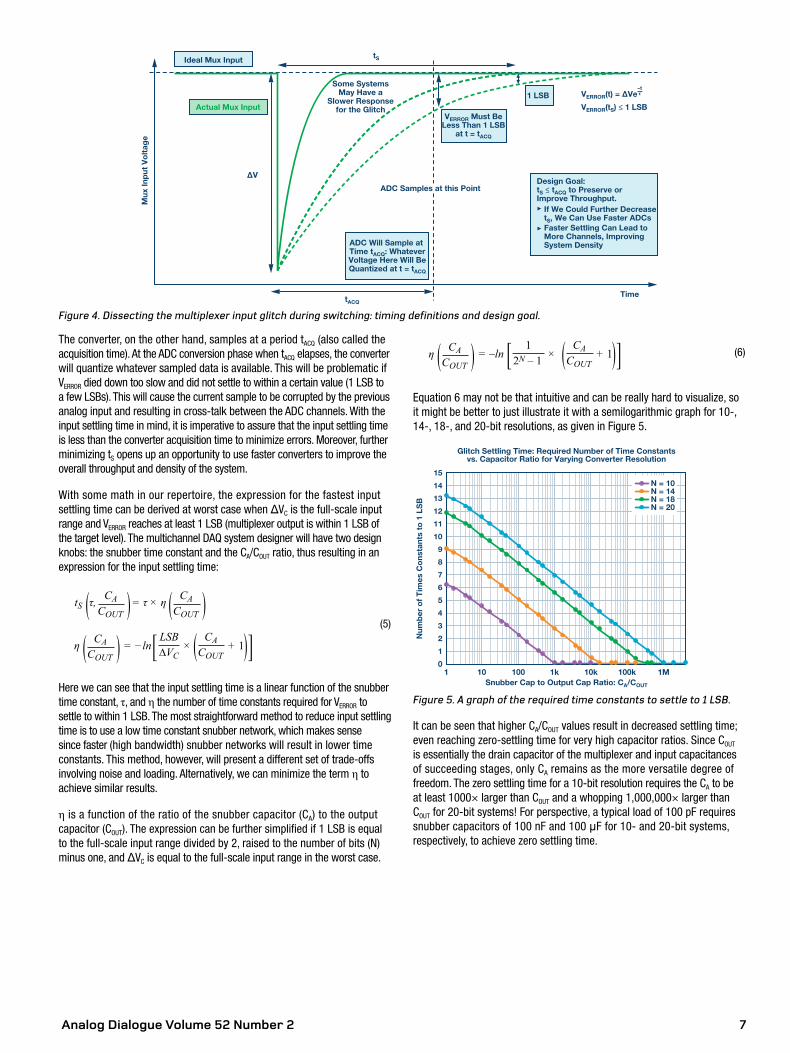
Equation 6 may not be that intuitive and can be really hard to visualize, so it might be better to just illustrate it with a semilogarithmic graph for 10-, 14-, 18-, and 20-bit resolutions, as given in Figure 5.
0
1
2
3
4
5
6
7
8
9
10
11
12
13
14
15
Num
ber
of
Tim
es C
ons
tant
s to
1 L
SB
1 10 100 1k 10k 100k 1MSnubber Cap to Output Cap Ratio: CA/COUT
Glitch Settling Time: Required Number of Time Constantsvs. Capacitor Ratio for Varying Converter Resolution
N = 10N = 14N = 18N = 20
Figure 5. A graph of the required time constants to settle to 1 LSB.
It can be seen that higher CA/COUT values result in decreased settling time; even reaching zero-settling time for very high capacitor ratios. Since COUT is essentially the drain capacitor of the multiplexer and input capacitances of succeeding stages, only CA remains as the more versatile degree of freedom. The zero settling time for a 10-bit resolution requires the CA to be at least 1000× larger than COUT and a whopping 1,000,000× larger than COUT for 20-bit systems! For perspective, a typical load of 100 pF requires snubber capacitors of 100 nF and 100 μF for 10- and 20-bit systems, respectively, to achieve zero settling time.
Ideal Mux Input tS
Some SystemsMay Have a
Slower Responsefor the Glitch
ADC Will Sample at Time tACQ: WhateverVoltage Here Will BeQuantized at t = tACQ
tACQTime
VERROR Must Be Less Than 1 LSB
at t = tACQ
VERROR(t) = ΔVe
VERROR(tS) ≤ 1 LSB1 LSB
–tτ
Design Goal:tS ≤ tACQ to Preserve orImprove Throughput.
ΔV
Actual Mux Input
Mux
Inp
ut V
olt
age
ADC Samples at this Point
If We Could Further Decrease tS, We Can Use Faster ADCsFaster Settling Can Lead to More Channels, Improving System Density
Figure 4. Dissecting the multiplexer input glitch during switching: timing definitions and design goal.
Analog Dialogue Volume 52 Number 28
In summary, minimizing the input settling time can be achieved through two methods:
1. Using high bandwidth for the snubber network
2. Using high values of CA with respect to COUT
High Bandwidth and a Large Snubber Capacitor Minimizes Input Settling Time, So Let’s Just Use the Highest Bandwidth and Largest CapacitorNo! You must consider the RC loading effects and the amplifier’s driving capability! In order to investigate the loading effects of the snubber network to the buffer amplifier, the analog front-end subsystem should be analyzed in the frequency domain.
Since we are building on the idea of first-order response for the input glitch, the snubber network pole should be the most dominant contributor. In other words, the snubber bandwidth should be less than both the buffer amplifier and the multiplexer to avoid multiple poles interacting, ensuring that the first-order approximation will hold.
VIN
VA
VA
ZRC
VOUT
CL
RA
SnubberNetwork
Amplifier
CA
VOUTVIN
ZOUT, AMP RA
CA
ZOUT, AMP(ω)RCL(ω) ZRC(ω)
RA
CL CA
Figure 6. The buffer and snubber equivalent circuit (left) and the equivalent impedance of the amplifier and snubber network (right).
A typical buffer architecture consists of a precision amplifier in a buffer (G = 1) configuration in cascade with the snubber network. Analyzing in the frequency domain, the output of this subsystem depends on the ratio of the snubber input impedance to the sum of the snubber input impedance and amplifier closed-loop output impedance. By inspection, the snubber input impedance should be greater than the amplifier’s closed-loop impedance to avoid loading effects, which is described in Equation 7.
jωRACA + 1jωCA
RCLjωRCLCL + 1
ZRC » ZOUT, AMP
»(7)
That is, to avoid the snubber network loading the buffer amplifier, we should:
1. Increase the snubber time constant, RACA, effectively decreasing the bandwidth
2. Use small snubber capacitor CA
3. Choose an amplifier with very low closed-loop output impedance
The first two options provide us with a clear understanding of the trade-offs between the loading effects and input settling time. This puts a limit
on how high we can go with the snubber bandwidth and capacitor. The third option introduces a performance parameter that should be taken into account when choosing the appropriate precision amplifier. Stability and driving capabilities should also be considered.
Figure 7 shows that for a precision amplifier that has enough bandwidth—say the ADA4096-2 with –3 dB closed-loop bandwidth of about 970 kHz—the results agree with the analysis presented so far, with the exception of a few waveforms. For a snubber bandwidth of 10 kHz, the largest CA resulted in the fastest input settling time. While for a snubber bandwidth of 200 kHz, increasing CA still results in faster settling time until loading takes effect. The underdamped response seen from the results features the minimum glitch magnitude but has longer settling time than the response from the smaller CA, despite higher glitch magnitude. This stresses the importance of carefully investigating how the snubber loads the amplifier, as this should always be taken into account when choosing the components for the system.
Figure 7. Multiplexer input for snubber bandwidth of 10 kHz (top) and 200 kHz (bottom) for ADA4096-2 amplifier model.
As presented earlier, one amplifier parameter to look at is the closed-loop output impedance. An operational amplifier typically has its closed-loop impedance inversely proportional to its open-loop gain A V. We also want a
Joseph Leandro Peje [ [email protected]] received his B.S. degree in computer engineering from the University of the Philippines—Diliman, Quezon City, Philippines, and is finishing up his master’s in electrical engineering, with a concentration in microelectronics, at the same university. He is currently an analog IC design engineer at Analog Devices in General Trias, Philippines, focusing on precision amplifiers and analog and mixed-signal systems verification.
Joseph Leandro Peje
high bandwidth for the snubber network for minimum settling time, requiring the amplifier to have a –3 dB bandwidth even greater than the snubber bandwidth. Aside from low noise, offset, and offset drift, a precision amplifier that is the most suited for use in multiplexed DAQ system for minimum input settling time has two more prioritized attributes: 1) has high bandwidth and 2) has very low closed-loop impedance. However, these do not come without trade-offs and they are in the form of power consumption. As examples, we can look at the closed-loop impedances of both the ADA4096-2, and ADA4522-2, shown in Figure 8.
1k
0.001
0.01
1
100
0.1
10
100 1 k 10k 100k 1M 10M 100M
Out
put
Imp
edan
ce (Ω
)
Frequency (Hz)
AV = 100AV = 10AV = 1
VSY = ±2.5 V to ±27.5 V
Figure 8a. Data sheet plots of the closed-loop impedance for ADA4522-2.
10k
1k
100
10
1
0.1
10 100 1k 10k 100k 1M 10M0.01
ZO
UT (Ω
)
Frequency (Hz)
ADA4096-2VSY = ±15 VTA = 25°C
G = 100
G = 10
G = 1
Figure 8b. Data sheet plots of the closed-loop impedance for ADA4096-2.
From the data sheet plots of the closed-loop output impedances, and with ADA4522-2’s –3 dB closed-loop bandwidth of 6 MHz (at nominal), it is clear that it is the more suitable driver for the application. But when power consumption is prioritized, ADA4096-2’s with supply current of 60 μA per amplifier (typical) is more attractive than ADA4522-2’s 830 μA per amplifier (typical). Nonetheless, both precision amplifiers can be used; it all just boils down on what the application really needs.
Conclusion
Alright, So What’s the Best That We Can Do?To maximize the density and throughput of multichannel DAQ systems, the input settling time should be less than or equal to the ADC acquisition time. Any additional delay diminishes the performance of multichannel DAQ systems. Minimizing the input settling time involves increasing the bandwidth and the capacitor of the snubber network, though care must be exercised when choosing component values due to loading effects in the frequency domain. Finally, selecting the most appropriate precision amplifier involves balancing the trade-off between power, closed-loop output impedance, and the –3 dB bandwidth, prioritizing what the application really requires.
References Corrigan, Theresa. AN-1024 Application Note: How to Calculate the Settling Time and Sampling Rate of a Multiplexer. Analog Devices, Inc., 2009.
Interactive Design Tool: Analog Switch Settling-Time Calculator. Analog Devices, Inc.
MT-088 Tutorial, Analog Switches and Multiplexers Basics. Analog Devices, Inc., 2009.
Acknowledgements Dan Burton, Vicky Wong, Peter Ohlon, Eric Carty, Rob Kiely, May Porley, Jess Espiritu, Jof Santillan, Patrice Legaspi, Peter Hurrell, and Sherwin Almazan.
As we now look to move up the stack with SiPs (system in packages), micromodules, and modules, you the customer are once again presenting us with new and novel measurement challenges—challenges that will force us to refine our measurement methodology and develop novel test and measurement solutions. SiPs leverage complex core technology and go to an unprecedented level of system integration by incorporating pas-sive and active components alongside, in some cases, a central processing unit for configuration and control. This level of integration introduces ever increasing functionality, embedded feature sets, advanced packaging, internal node access issues, embedded software, and system-level calibration to name a few. These solutions simplify the user experience of our complex converter products; but the complexity is handled and the design and measurement barriers are overcome within ADI.
The Past and PresentA prime example of recent test and measurement challenges would be the advancements in our low power Σ-Δ portfolio. To showcase the advancements made, Figure 1 highlights the fact that we have now reached a level of system on chip that is far beyond previous generations of converters. Our latest release in this product family is a low power, low noise, completely integrated analog front end for high precision measurement applications. The degree of signal chain integration in this product demands measurement expertise in the 24-bit, Σ-Δ analog-to-digital converter (ADC) domain, in reference performance and accuracy, in channel sequencing and timing, in digital feature and functionality, and in oscillator performance. Figure 1 compares the 24-bit ADC to a 16-bit predecessor that was considered to have breakthrough performance in its time. for its time. Its challenges have been resolved and today’s technology has progressed by orders of magnitude. Unless the progress in technology is matched by our test and measurement capabilities, then the work to maintain technology leadership in the industry will amount to nothing.
IntroductionMoving up the stack has been an implicit part of ADI’s strategy for many years—but recently, through a focus on delivery of more solutions, this strategy has become explicit. If you consider our roots, there was a time when we supplied only discrete components with data sheets. Our new philosophy is to engage and understand the whole of the problem we are trying to solve for you, our customer. As part of this philosophy, measurement engineering at ADI is going beyond traditional approaches of just testing an IC to testing solutions, including software, signal chain systems in package, micromodules, and other elements. This approach will ensure that we are developing solutions that will create significant value for our customers.
Within ADI, measurement engineering teams are sometimes viewed as the people who develop hardware and software to get product out. However, the measurement function, consisting of test and evaluation engineering, is one of the most challenging engineering disciplines at ADI today. Measurement engi-neers are the people who underpin a company’s contract with customers. They are the ones you trust when looking at guaranteed maximum and minimum device specifications, typical performance, max ratings, and robustness. With ever increasing performance from our design teams, we rely on the experience that measurement engineering has to keep pace with these improvements in performance vectors, be it speed, noise, power, or new integrated features.
The measurement discipline, consisting of test and evaluation engineering, works under the challenges of breakthrough performance, on-time delivery, and increasing quality requirements. Not so long ago we were dealing with simple, single-function ICs (converters) with 10- or 12-bit precision. Today, 20-bit SAR converters, 20-bit DAC converters, and 32-bit Σ-Δ converters show how the measurement challenges have changed as IC technologies have developed over the last number of years. To illustrate the degree of change, we will look at the evolution of our low power Σ-Δ products to help demonstrate the completeness of signal chain integration achieved, and to highlight the demands and advancements this has forced in our measurement capabilities.
Moving Up the Stack Challenges for Measurement Engineering at ADIBy Noel McNamara, Martina Mincica, Dominic Sloan, and David Hanlon
Rail-to-Rail Analog Inputs, Internal Clock Oscillator, Bias Voltage Generator Simultaneous 50 Hz/60 Hz Rejection, Multiple Filter Options Diagnostic Functions, Self and System Calibration, Sensor Burnout Detection Crosspoint Multiplexed Analog Inputs, Automatic Channel Sequencer, Per Channel Configuration Bandgap Reference, Programmable Excitation Currents, Internal Temperature Sensor User Selectable 3× Power Scaling
Pre-2014 2015Vintage
Mea
sure
men
t C
halle
nge
An in-depth understanding of converter architecture and expertise in mixed-signal test circuit design, PCB layout techniques, and measurement software allow us to obtain the optimum performance from these highly integrated converters. This enables the development of SiPs/modules where our experience can be harnessed to solve more of the customers design challenges and to reduce their development time.
The Present and Future
So, as we step forward into solving the problems of tomorrow for our customers, we have a toolbox armed with a wealth of products and mea-surement expertise. Throughout ADI’s history we have consistently achieved breakthroughs in real-world signal processing and are continually expanding our core technologies with on-chip integration. In more recent times we’ve ventured into DSP, RF, and MEMS and are now breaking new ground in emerging fields such as IoT.
The ADI acquisition of Linear Technology pushes this further by combining our strong portfolios and adding industry-leading, high performance analog and power solutions. This reinforces our positioning to integrate these technologies, impacting our customers with solutions that truly demon-strate our capabilities.
Figure 1. Evolution of integration: progression of performance driving innovation.
Analog Dialogue Volume 52 Number 212
Figure 2 shows our progression in amassing technologies on the horizontal and in the vertical, where we are now using these building blocks in SiP/module developments to go beyond silicon. The measurement engineer is enabling this by combining our expertise in these core technologies.
So why do we at ADI think this is necessary? From engaging our customers, we understand that they too are evolving; you are also moving up the stack. The landscape is changing; your mixed-signal design teams may be smaller, you may have focus and expertise elsewhere, and you are looking to shorten your design cycles and time to market. ADI can unburden you from these design challenges by providing you with complete signal chains, and this needs to be underpinned with effective measurement solutions.
Prototyping Module SolutionsThrough early engagement and collaboration with our customers, measurement engineers can leverage our hardware expertise to prototype our SiP/module designs. We can establish a proof of concept for novel ideas and quickly debug, evaluate, and, if necessary, iterate the schematic and layout to achieve the optimum performance. We can employ mission testing, evaluating the customer’s sensors and testing the full system in specific application use cases, as well as analyzing the data to ensure that all requirements are being met prior to the final SiP or module being developed.
Amplifiers
Mission Testing Stimulus
Sig
nal S
tim
ulus
Mission Testing Stimulus
MeasurementInstruments
DataAnalysis
Prototype PCB
VoltageReferences
SwitchesMux
PowerManagement
Converters
SiPs/Modules
Isolators
Processors
Figure 3. Module testing prototype.
These prototypes also allow us to develop our ATE solutions, allowing us to crack the new test challenges that these system-level devices can pose: for example, package form factors, test node access points, or even firm-ware interfacing.
Through our experience with the core technologies of the blocks that compose these products, we can use our component-level know-how to achieve the best performance from these parts and even push the system-level perfor-mance to new levels. The prototype enables us to easily interface with bench stimulus and measurement instruments, and assess where test node access is required for production testing. This prototype can allow us and, indeed, you our customers to begin verification of system-level calibration of the full system signal path.
Mission Testing
Module Prototype
Firmware Access
Figure 4. Example prototype board for module testing.
As SiPs/modules evolve and where a processor is required for configurabil-ity, control, algorithm processing, and to unburden customers of complexity, firmware development may be required. This can begin and evolve with the prototype. Through development and testing of the firmware, measurement engineers apply their troubleshooting mindset to detect bugs and anticipate what could cause issues. This can feedback in o the system design and allow advancement. This prototype can showcase the idea to customers and this can spark feedback that can also determine the module development direction. In this way, the customer can influence the solution from early stages.
ConclusionThe measurement teams at ADI have extended our capabilities over the years as the core technology has continued to grow in complexity and integration. We are now testing so much more than a core converter and integration in the silicon has in turn led to advancement in measurement techniques and technology. Our measurement solutions in the lab and for production testing have advanced along with the technology. Combining our measurement expertise in core converters, sensors, amplifiers, references, power, and digital technology keeps us ahead of what’s possible.
Looking to the future, ADI continues to move up the stack with ongoing development of multichip SiPs, modules, and micromodules. These modules move the technology up the stack to another level presenting new challenges for measurement engineering, whilst simultaneously reducing the engineering burden on our customers. Simplifying the customer application development journey is central to ADI’s technology. We have broadened and continue to broaden the measurement skill base to leverage our expertise in support of these new technologies. Whether it is through prototype PCB design, mission testing, firmware development, or prototype demonstration, the measurement engineers at ADI are key to the success of these products.
As this advancement in our technology offering gathers pace, the ADI measurement community is one step ahead to ensure world-class measurements are delivered alongside world-leading technology.
Analog Dialogue Volume 52 Number 2 13
Noel McNamara [[email protected]] is a test engineer in the Precision Converter Group at Analog Devices in Limerick.
Noel McNamara
Martina Mincica [[email protected]] is a design evaluation engineer in the Precision Convertor Group at Analog Devices in Limerick. She joined in 2011 after receiving her B.S.E.E., M.S.E.E., and Ph.D. in electronic engineering from Univer-sity of Pisa, Pisa, Italy, in 2004, 2007, and 2011, respectively. Her field of interest at the time was radio frequency integrated circuit design. Since then she has been working on precision DAC and ADC bench evaluation.
Martina Mincica
Dominic Sloan [[email protected]] is a design evaluation engineer in the Precision Convertor Group at Analog Devices. He joined ADI in 2007, moving from a role in product design at a medical devices company. He graduated from the Limerick Institute of Technology in 2000 with a City & Guilds advanced technician diploma in electronic engineering, and then worked in a high volume manufacturing environment in the telecommunications industry before going on to receive a bachelor’s of engineering in electronics at the University of Limerick.
Dominic Sloan
David Hanlon [[email protected]] is a test engineer in the Precision Convertor Group at Analog Devices in Limerick. He joined Analog Devices in 1998 after receiving his bachelor’s of engineering from the Dublin Institute of Technology and has been working on high performance mixed-signal converters ever since.
buffers. The band gap and two output buffers are powered separately to provide exceptional isolation. Each output buffer has a Kelvin sense feedback pin for optimum load regulation.
0.1 µF
1 µF
1 µF
1 µF
400 Ω
1 µF
VIN
5 V to 13.2 V
VOUT1_F
VIN1
Bypass
LT6658-2.5
VOUT1_S
VOUT2_F
VIN2
Band Gap VOUT2_S
GNDNR
VOUT22.5 V
50 mA
VOUT12.5 V
150 mA
Figure 1. Typical application.
The noise reduction stage consists of a 400 Ω resistor with a pin provided for an external capacitor. The RC network acts as a low-pass filter, bandlimiting the noise from the band gap stage. The external capacitor can be arbitrarily large, reducing the noise bandwidth to a very low frequency.
Fast and Quiet Response to Load StepsAs a regulator, the LT6658 supplies 150 mA from the VOUT1_F pin with excellent transient response. Figure 2a shows the response to a 1 mA load step transient from 10 mA to 11 mA; Figure 2b shows the response to a 140 mA load step from 10 mA to 150 mA. The source and sink capability of the output buffer enables fast settling of the output. The transient response is short, while excellent load regulation is maintained. Load regulation is typically only 0.1 ppm/mA. The second output, VOUT2_F, has a similar response with a 50 mA maximum load.
Precision analog designers often lean on the quietly humble voltage reference to power their DAC and ADC converters. This job lies outside the fundamental purview of a reference—ostensibly designed to provide a clean, precise stable voltage to an actual power source; namely a power converter’s reference input. With some caveats, references are usually up to the task of providing precise voltage to the converter’s reference input, emboldening designers to ask references to power increasingly higher current applications. After all, if the reference can power the converter, why not the analog signal chain, or another converter, and on down the list?
The choice between precision and power comes up often in any design process. The brute force approach to making this decision suggests using a reference when precision is demanded, and an LDO when milliwatts of power are required. Besides the additional board space and cost, separate signals must be routed, even if their nominal voltages are the same. And if a high precision voltage source is required to provide milliwatts of power, the designer is forced to buffer a reference. The LT6658 solves this dilemma by providing two low noise precision outputs with a combined 200 mA output current and world-class reference specifications.
About the LT6658 Reference Quality Low Drift RegulatorThe LT6658 is a precision low noise, low drift regulator featuring the accuracy specifications of a dedicated reference and the power capability of a linear regulator—combining the traits of both into ADI’s Refulator™ technology. The LT6658 boasts 10 ppm/°C drift and 0.05% initial accuracy, with two outputs that can support 150 mA and 50 mA, respectively, each with 20 mA active sinking capability. To maintain accuracy, load regulation is 0.1 ppm/mA. Line regulation is typically 1.4 ppm/V when the input voltage supply pins are tied together and less than 0.1 ppm/V when the input pins are provided with independent supplies.
To better grasp the LT6658’s features and how it achieves its level of performance, a typical application is shown in Figure 1. The LT6658 consists of a band gap stage, a noise reduction stage, and two output
The Refulator: The Capabilities of a 200 mA Precision Voltage ReferenceBy Michael Anderson
Output TrackingFor applications with multiple converters using different voltage references, the LT6658 outputs track, even if the outputs are set to different voltages—ensuring consistent conversion results. This is possible because the two outputs of the LT6658 are driven from a common voltage source. The output buffers are trimmed, resulting in excellent tracking and low drift. As the load on VOUT1_F increases from 0 mA to 150 mA, the VOUT2 output changes less than 12 ppm as shown in Figure 3. That is, the relationship between the outputs is well maintained even over varying load and operating conditions.
VOUT1 Load Current (mA)
1 10 100 5000
2
4
6
8
10
12
14
16
18
20
VO
UT
2 V
olt
age
Cha
nge
(pp
m)
Figure 3. Channel-to-channel load regulation (effect of heating removed).
Power Supply Rejection and IsolationTo facilitate exceptional power supply rejection and output isolation, the LT6658 provides three power supply pins. The VIN pin supplies power to
the band gap circuit while VIN1 and VIN2 supply power to VOUT1 and VOUT2, respectively. The simplest approach is to connect all three supply pins together, delivering a typical dc power supply rejection of 1.4 ppm/V. When the power supply pins are connected separately and the VIN1 supply is toggled, the dc line regulation for VOUT2 is 0.06 ppm/V.
Table 1 summarizes power supply rejection as each of the power supply pins are changed from 5 V to 36 V. The VIN supply has the most sensitivity, causing a typical 1.4 ppm/V change on the outputs. Supply pins VIN1 and VIN2 have almost no effect. The measurements in the VIN1 and VIN2 columns are at the level of the output noise.
Two examples of ac PSRR are shown in Figure 4. The first example has a 1 μF capacitor on the NR pin while the second example includes a 10 μF capacitor on the NR pin. The larger 10 μF capacitor extends the 107 dB rejection to 2 kHz.
Frequency (kHz)
0.01 10.1 10 1k1000
20
40
60
80
100
120P
SR
R (d
B)
VIN = VIN1 = VIN2 = 6 V
COUT1 = 1 µFILOAD = 0 A
CNR = 1 µFCNR = 10 µF
Figure 4. Power supply ripple rejection.
The ac channel-to-channel power supply isolation from VIN1 to VOUT2 is shown in Figure 5. Here the channel-to-channel power supply isolation is greater than 70 dB beyond 100 kHz when CNR = 10 μF.
Frequency (kHz)
0.01 10.1 10 1000
20
40
60
80
100
120
140
Cha
nnel
-to
-Cha
nnel
Iso
lati
on
(dB
)
COUT2 = 1 µFCNR = 10 µF
COUT1 = 1 µFCOUT1 = 10 µF
Figure 5. Channel-to-channel VOUT1 to VOUT2 isolation.
Analog Dialogue Volume 52 Number 216
Load transients have a minimal effect on the adjacent output. Figure 6a and Figure 6b illustrate channel-to-channel output isolation. One output is wiggled at 50 mV rms, and the change in in the other is plotted.
Frequency (kHz)
0.001 10.1 10 1k1000
20
40
60
80
100
120
140
VO
UT
2 C
hann
el-t
o-C
hann
el Is
ola
tio
n (d
B)
50 mV rms Signal on VOUT1
ILOAD1 = 150 mAILOAD1 = 0 mA
Figure 6a. Channel-to-channel VOUT1 to VOUT2 load isolation.
Frequency (kHz)
0.001 10.1 10 1k1000
20
40
60
80
100
120
140
VO
UT
1 C
hann
el-t
o-C
hann
el Is
ola
tio
n (d
B)
50 mV rms Signal on VOUT2
ILOAD2 = 50 mAILOAD2 = 0 mA
Figure 6b. Channel-to-channel VOUT2 to VOUT1 load isolation.
Extraordinary ac PSRR can be achieved using the circuit shown in Figure 7. The VOUT1 output bootstraps the supplies VIN and VIN2, resulting in a recursive reference.
1 µF
1 µF10 kΩ
10 kΩ
1 µF
10 µF
10 µF
400 Ω
1 µF
VIN
7.5 V to 36 V
VOUT1_F
VIN1
Bypass
LT6658-2.5
VOUT1_S
VOUT2_F
VIN2
Band Gap VOUT2_S
GNDNR
VOUT22.5 V
VOUT15 V
1.5 kΩ1 W
4.7 V1N5230
1N4148
1N4148
Figure 7a. Recursive reference solution (VOUT1 supplies power to VIN and VIN2).
Frequency (kHz)
0.001 0.10.01 1 100100
20
40
60
80
100
120
140
160
180
Po
wer
Sup
ply
Rej
ecti
on
Rat
io (d
B)
VOUT1 VOUT2 Theoretical
Figure 7b. AC PSSR for the recursive reference circuit.
Power Management and ProtectionThe three supply pins help manage the amount of power dissipated in the package. When supplying a large current, lower the supply voltage to minimize the power dissipation in the LT6658. Less voltage will appear across the output device, resulting in less power consumption and higher efficiency.
Output disable pin OD turns off the output buffers and places the VOUT_F pins in a high impedance state. This is useful in the event of a fault condition. For example, a load may become damaged and shorted. This event can be sensed by external circuitry and both outputs can be disabled. This feature can be ignored and a weak pull-up current will enable the output buffers when the OD pin floats or is tied high.
The LT6658 comes in a 16-lead MSE exposed pad package with a θJA as low as 35°C/W. When the supply voltage is high, power efficiency is low, resulting in excessive heat in the package. For example, a 32.5 V supply voltage at full load produces 30 V × 0.2 A of excess power across the output devices. Six watts of excess power would raise the internal die temperature to a dangerous 210°C above ambient. To protect the part, a thermal shutdown circuit disables the output buffers when the die temperature exceeds 165°C.
NoiseFor data converter and other precision applications, noise is an important consideration. The low noise LT6658 can be made even lower with the addition of a capacitor on the NR (noise reduction) pin. A capacitor on the NR pin forms a low-pass filter with an on-chip 400 Ω resistor. A large capacitor lowers the filter frequency and subsequently, the total integrated noise. Figure 8 shows the effect of increasing the values of the capacitor on the NR pin. With a 10 μF capacitor, the noise rolls off to about 7 nV/√Hz.
Frequency (kHz)
0.01 10.1 10 1k 10k1000
25
50
75
100
125
150
175
Out
put
Vo
ltag
e N
ois
e (n
V/√
Hz)
CNR = 0.1 µFCNR = 1 µFCNR = 10 µF
COUT1 = 1 µF
Figure 8. Noise reduction by increasing CNR.
Analog Dialogue Volume 52 Number 2 17
By increasing the output capacitor, the noise can be further reduced. When both the NR and output capacitors are increased, the output noise can be reduced down to a few microvolts. The LT6658 is stable with output capacitance between 1 μF and 50 μF. The output is also stable with large capacitance if a 1 μF ceramic capacitor is placed in parallel. For example, Figure 9a shows a circuit with 1 μF ceramic capacitor in parallel with a 100 μF polyaluminum capacitor. This configuration remains stable while lowering the noise bandwidth. Figure 9b illustrates the noise response for different values of output capacitance. In all three cases, there is a small 1 μF ceramic capacitor in parallel with the larger capacitor.
C11 µF
C2100 µF
LT6658-2.5
VOUT1_F
VOUT1_S
Figure 9a. Noise reduction by increasing C1.
Frequency (kHz)
0.01 10.1 10 1k 10k1000
25
50
75
100
125
150
175
Out
put
Vo
ltag
e N
ois
e (n
V/√
Hz)
C1 = 1 µFC1 = 10 µFC1 = 100 µF
CNR = 1 µF
Figure 9b. Noise reduction by increasing C1.
One drawback of this scheme is the noise peaking, which can add to the total integrated noise. To reduce the noise peaking, a 1 Ω resistor can be inserted in series with the large output capacitor as shown in Figure 10a. The output voltage noise and total integrated noise are shown in Figures 10b and 10c, respectively.
C11 µF
C2100 µF
R11 Ω
LT6658-2.5
VOUT1_F
VOUT1_S
Figure 10a. Reduce noise peaking by adding a 1 Ω resistor in series with C2.
Figure 10b. Reduce noise peaking by adding a 1 Ω resistor in series with C2.
C1 (µF)
1 10 100 3000
2.0
1.5
1.0
0.5
2.5
3.0
3.5
4.0
Inte
gra
ted
No
ise
(µV
rm
s)
Figure 10c. Reduce noise peaking by adding a 1 Ω resistor in series with C2.
ApplicationsThe LT6658 provides quiet, precise power for a number of demanding applications. In the mixed-signal world, data converters are often controlled by microcontrollers or FPGAs. Figure 11 illustrates the general concept. Sensors provide signals to analog processing circuits and converters, all of which need clean power supplies. The microcontroller may have several supply inputs including analog power.
As a general rule, noisy digital supply voltages for the microcontroller should be isolated from the clean, precise analog supply and reference. The two outputs of the LT6658 provide excellent channel-to-channel isolation, power supply rejection, and supply current capability, ensuring clean power to multiple sensitive analog circuits.
Analog Dialogue Volume 52 Number 218
The LT6658 is also well suited to industrial environments since it can operate with noisy supply rails and where load glitches due to conversions on one output have little influence on the adjacent output. Moreover, when a load demands current on one output, the adjacent output continues to track.
A real-world example is shown in Figure 12, where the LTC2379-18 high speed ADC circuit is operated with an LT6658. The Kelvin sense input on VOUT2 is configured to gain up the 2.5 V output to a 4.096 V reference voltage and to provide a common-mode voltage to the input amplifier, LTC6362. VOUT1 is gained up to 5 V, providing power to the LTC6362 and other analog circuits that require a 5 V rail. Both LT6658 outputs have the maximum load at 150 mA and 50 mA on VOUT1 and VOUT2, respectively.
Table 2. Data Acquisition Circuit Example from Figure 12
Parameter 16-Bit SAR 18-Bit SAR
SNR 92.7 dB 97.5 dB
SINAD 92.1 dB 95.9 dB
THD −101.2 dB −101.1 dB
SFDR 101.6 dB 103.2 dB
ENOB 15.01 bits 15.64 bits
The circuit in Figure 13 illustrates how the LT6658 can power noisy digital circuits while maintaining a quiet, precise reference voltage for a precision ADC. In this application, the LT6658 or a separate LDO supplies a 3.3 V rail to a noisy FPGA supply (VCCIO) and some miscellaneous logic on one channel, and 5 V to the reference input of the 20-bit ADC on the other channel.
Mike Anderson [[email protected]] is a senior IC design engineer with Analog Devices and most recently with Linear Technology Corporation, where he works on signal conditioning products such as precision references and amplifiers. He previously worked as a senior member of technical staff and section lead at Maxim Integrated Products, designing ADCs and mixed-signal circuits. Prior to 1997, Mike worked at Symbios Logic as a principle IC design engineer designing high speed fiber channel circuits. He received a B.S.E.E. and an M.S.E.E. from Purdue University. Mike holds 16 patents and occasion-ally publishes articles.
Michael Anderson
LT6658–2.5Regulator
ADC Counts
–12 0–10 –8 –6 –4 –2 2 4 6 8 10 120
50
100
150
200
250
300
350S
amp
les
Figure 14. Histogram test results of the circuit in Figure 13.
By switching the digital supply between the LT6658 and the LDO, we can assess how well the LT6658 isolates digital noise on one channel from the channel driving the quiet reference input of the 20-bit ADC. Using a clean dc source on the input of the ADC, the noise can be inferred as shown in Figure 14. The histogram shows no appreciable difference in results between the LT6658 or the LDO supplying power to the VCCIO pins of the FPGA, demonstrating the LT6658’s robust regulation and isolation.
ConclusionThe LT6658 is the next step in the evolution of references and regulators. The precision performance and ability to provide a combined 200 mA of current from a single package is a paradigm shift for precision analog power. Noise rejection, channel-to-channel isolation, tracking, and load regulation make this product ideal for precision analog reference and power solutions. With this new approach, applications do not need to compromise precision or power.
Figure 1 shows an AD5453 14-bit MDAC with a downstream amplifier that can amplify or weaken the signal based on the DAC’s programmed code.
Circuit CalculationThe output voltage (VOUT) for the circuit is calculated as follows:
D2nVOUT = –Gain × VIN ×
The output voltage is affected or bounded by the operational amplifier’s supply voltage, apart from the gain and the set code D of the DAC. In the case shown, the ADA4637-1 amplifier supplied with ±15 V should output a maximum voltage of ±12 V to leave it an adequately large control range. The gain is determined via the resistors R2 and R3:
R2 + R3
R2Gain =
Question:How could a multiplying DAC be used other than as a DAC?
Answer:Most digital-to-analog converters (DACs) are operated with a fixed positive reference voltage and output voltage or a current that is proportional to the product of the reference voltage and a set digital code. With so-called multiplying digital-to-analog converters (MDACs), this is not the case. Here, the reference voltage can vary, often in the range of ±10 V. The analog output can then be influenced via the reference voltage and the digital code—in both cases dynamically.
ApplicationsWith the corresponding wiring, the module can output a signal that is amplified, damped, or inverted with respect to the reference. This yields applications in the fields of waveform generators, programmable filters, and PGAs (programmable gain amplifiers), as well as many other applications in which offset or gain must be adjusted.
Rarely Asked Questions—Issue 152Problem Solver: Multiplying Digital-to-Analog ConverterBy Thomas Tzscheetzsch
All resistors (R1 to R3) should have the same temperature coefficient of resistance (TCR), which, however, does not have to be the same as the TCR of the DAC’s internal resistors. The resistor R1 is used to adjust the internal resistor (RFB) in the DAC to the resistors R2 and R3 according to the following relationships:
R1 + RFB = RFB + R2 || R3R1 = R2 || R3
The resistors must be selected in such a way that the op amp is still within its operating range at the maximum input voltage (the DAC can handle ±10 V at VREF). It should also be noted that the amplifier’s input bias current (IBIAS) is multiplied by the resistance (RFB + R2 || R3) and that this has a considerable effect on the offset voltage. For this reason, the ADA4637-1 op amp with a very low input bias current and a very low input offset voltage according to the data sheet that was selected. To prevent instabilities in the closed-loop control system or so-called ringing, the 4.7 pF capacitor was inserted between IOUT and RFB; this is especially recommended for fast amplifiers.
As mentioned earlier, the offset voltage of the amplifier is multiplied by the closed-loop gain. When the gain is set with the external resistors changes
by a value corresponding to a digital step, this value is added to the desired value, producing a differential nonlinearity error. If it is large enough, it can lead to nonmonotonic behavior of the DAC. To avoid this effect, it is necessary to select an amplifier with a low offset voltage and a low input bias current.
Advantages over Other CircuitsIn principle, standard DACs can also be used if an external reference is allowed, but there are a few major differences between them and MDACs. Standard DACs can only process unipolar voltages of limited amplitude at the reference input. Apart from the amplitude, the reference input bandwidth is very limited. This is indicated on the data sheet by the multiplying bandwidth value. For the AD5664 16-bit DAC, for example, this value is 340 kHz. Multiplying DACs can use bipolar voltages, which can also be higher than the supply voltage, at the reference input. The bandwidth is also much higher—typically 12 MHz for the AD5453.
ConclusionMultiplying digital-to-analog converters are not that widespread, but they offer numerous possibilities. Apart from the self-built PGA with a high bandwidth, mobile applications are also very suitable applications because of their low power requirements of less than 50 μW.
Also by this Author:
Dynamic Use of the Disable Pin on an Amplifier
Volume 52, Number 1
Thomas Tzscheetzsch [[email protected]] joined Analog Devices in 2010, working as a senior field applications engineer. From 2010 to 2012, he covered the regional customer base in the middle of Germany and, since 2012, has been working in a key account team on a smaller customer base. After the reor-ganization in 2017, he’s leading a team of FAEs in the IHC cluster in CE countries as FAE manager.
At the beginning of his career, he worked as an electronics engineer in a machine building company from 1992 to 1998, as head of the department. After his study of electrical engineering at the University of Applied Sciences in Göttingen, he worked at the Max Planck Institutes for solar system research as a hardware design engineer. From 2004 to 2010, he worked as an FAE in distribution and worked with Analog Devices’ products.
Solar generation, energy storage, and domestic consumption in a typical, 24-hour day is illustrated in Figure 1. Figure 1 is the primary reason why systems are designed for bill management in a solar system. During nighttime when there is no irradiation on the solar panel, energy consumed will be purchased from the grid where the grids are lowest. As soon as the sun rises irradiation appears on the solar panels, power is generated, and domestic self-consumption begins where any solar generation is either used in the household or is diverted to charge the energy storage unit. This allows bill costs to be controlled by reducing the energy drawn from the grid and using solar generated energy where low feed-in tariff areas are available from utility companies.
Figure 1. Solar generation, energy storage, and domestic consumption in a typical 24-hour day.
RS-485 is the communication application of choice for PC screen data updates such as current power, current consumption in the maximum power point trackers, battery charge and health, and CO2 reduction, etc., are available, as can be seen in Figure 2.
New government policy combined with new regulation is driving renewable energy generation, and the solar market is expected to have strong growth in the future. Due to the current increase of power density in solar inverters and the demand for energy storage balancing, this generation of solar power leads to a need to significantly monitor all elements of a solar system. For solar PV applications, RS-485 communications are used due to inherent noise immunity. Adding iCoupler® isolated RS-485 transceivers provides a safe, reliable, and EMC robust solution for solar PV network communication interfaces.
RS-485 has several uses, the primary use being remote monitoring of power generation, power point trackers, and energy storage status (battery storage).
For solar applications like energy storage communications is critical, as it alerts the user of power generation and consumption activities within their solar installation. Several systems strategies may be installed such as bill management, PV self-consumption, demand charge reduction, and backup power. Backup power is the most popular, especially in the U.S., due to the various hurricanes causing havoc in the states of Texas and Florida.
Table 1. Domestic Energy Storage Strategies
Domestic Energy Storage Strategy
Definition
Bill Management Time of Use (TOU)
Minimizes electricity purchases during peak electric-ity consumption hours, while TOU shifts purchases to lower rates behind the meter customers. The goal of this strategy is to reduce the customer’s bill.
PV Self ConsumptionMinimize the export of electricity generated by be-hind-the-meter PV systems to maximize the financial benefits in PV areas where utility rates are high.
Demand Charge Reduction
Reduce costs when utility companies charge excessively during peak times so customers can store energy.
Backup Power
This is a more common strategy and is the charging of any storage capable devices to use when the grid is down or at night time. This is more a backup pow-er strategy, where low utility charges are available at peak times and there are a low feed-in tariffs.
iCoupler Isolated Communication Solutions for Essential Monitoring of Solar PV and Energy StorageBy Richard Anslow and Martin Murnane
Current Power Energy Generation Current Consumption
12°C361 VpK
Grid Voltage Weather Configuration
Figure 2. Typical PV monitoring system data from a PV solar system.
Figure 3 illustrates a typical solar system with input-for-input dc strings, dc-to-ac conversion, energy charging and storage, and battery manage-ment and communications. Analog Devices offers a complete power, ommunications, and control interface signal chain solution for solar PV and energy storage applications. iCoupler isolated gate driver solutions include the ADuM4135 and ADuM4223/ADuM3223; iCoupler isolated communication port solutions include the ADM2795E, ADM2587E, and ADM3054; and mixed-signal processor solutions include the ADSP-CM419.
Why Use RS-485 Transceivers with iCoupler Isolation?iCoupler isolation provides a safe, reliable, and an EMC robust solution for solar PV network communication interfaces.
For solar PV networks the RS-485 or CAN communications interfaces often run over long cables in an electrically noisy environment. RS-485 communications are differential in nature and inherently noise immune. Adding iCoupler isolation increases noise immunity.
X The iCoupler family of digital isolation products has been tested and approved by various regulatory agencies, including UL, CSA, VDE, TÜV, CQC, ATEX, and IECEx. This regulatory agency testing provides a certi-fied level of safety in the presence of high voltage transients and elec-trical surges that can occur in electrically harsh solar PV environments.
X The solar PV communications interface usually operates at low data rates—less than 500 kbps—which is an ideal operating range for RS-485 communications. Alternative implementations such as Ethernet operate at fixed data rates of 10 Mbps/100 Mbps or 1 Gbps, which are clearly overdesigned for the application requirement.
X iCoupler isolation has proven EMC robustness, which reduces field fail-ures. Added EMC robustness reduces design and test time for interface circuits, allowing faster time to market for solar PV networks.
Battery Management System(BMS)
ADSP-CM419BGA
Resonant DC-to-DC Charger
ADuM4223/ADuM3223
VBATT – 1000 V
RS-485CAN
Grid
CAN
PV Boost 3-Phase ANPC Inverter and Safety Disconnect
ADuM4135ADuM4135
Act
ive
Cel
lB
alan
cing
SPI Isolated SPI
1500 V
RS-485
CAN
SPI Isolated CAN
ADuM4223/ADuM3223
ADuM4223/ADuM3223
ADuM4223/ADuM3223
Figure 3. Block diagram of a typical solar system with storage.
Drop-In iCoupler Isolation Solution for Existing Solar PV NetworksFor existing installations of solar inverters, which do not include iCoupler isolation robustness on the communications port, the iCoupler isolated RS-485 repeater is a powerful drop-in solution. The compact, signal, and power iCoupler isolated RS-485 repeater delivers robust isolation protection against electrical noise in electromagnetic capability (EMC) harsh solar environments.
The iCoupler isolated RS-485 repeater design consists of two RS-485 transceivers and two high speed ADCMP600 comparators. The ADM2587E
is a fully integrated signal and power isolated data transceiver with ±15 kV ESD protection, and is suitable for high speed communication on multipoint transmission lines. The ADM2587E includes an integrated, isolated dc-to-dc power supply, which eliminates the need for an external dc-to-dc isolation block. An RS-485 repeater requires flow control, which is essential for controlling the direction of communication on the RS-485 bus. Using the ADCMP600 high speed comparator allows high speed flow control and directionality on the ADM2587E logic pins, which results in a reliable communication system. For complete design guidelines please refer to AN-1458 Application Note: Isolated RS-485 Repeater with Automatic Direction Control.
ADM2587E
TxD
A
B
Y
Z
DE
VCC VISOOUT
VISOIN
RxD
RE
IsolationBarrier
Transceiver
GND1 GND2
Encode
Encode
Decode
Decode
R
D
Decode
Encode
Oscillator Rectifier
Regulator
Digital Isolation iCoupler
RT
ROREDE
A
DI
GND
B
R
D
GNDR
D
A B
RORE DE DI
Flow ControlLogic Circuit
Using ADCMP600
ADM2587E Signal and Power IsolatedRS-485 Transceiver
IsolationBarrier
IsolationBarrier
Signal and Power Isolated RS-485 RepeaterExtends Cable Length and Provides
Robustness for Fieldbus Applications
RT
A
B
GND2
GND2
RD
A B
RORE DE DI
1200 m Cable Length with256 RS-485 Transceivers
1200 m Cable Length with256 RS-485 Transceivers
Flow ControlLogic Circuit
Using ADCMP600
ADM2587E Signal and Power IsolatedRS-485 Transceiver
IsolationBarrier
IsolationBarrier
isoPower® DC-to-DC Converter
ADM2587E
TxD
A
B
Y
Z
DE
VCC VISOOUT
VISOIN
RxD
RE
IsolationBarrier
Transceiver
GND1 GND2
Encode
Encode
Decode
Decode
R
D
Decode
Encode
Oscillator Rectifier
Regulator
Digital Isolation iCoupler
isoPower DC-to-DC Converter
RT
ROREDE
A
DI
GND
B
R
D
GND
DI RODE RE DI RODERE
RT
A
B
GND2
GND2
R RD D
B A B A
Figure 4. Signal and power iCoupler isolated RS-485 repeater.
iCoupler Signal Isolated RS-485 Transceiver with Additional EMC RobustnessWhen designing an EMC communications interface, the circuit designer is often faced with a design and test iterative cycle. The circuit needs to be designed to meet system-level EMC standards and customer requirements. System-level IEC standards, such as IEC 61131-2 for industrial automation, specify varying levels of protection against IEC ESD, EFT, and surge, as well as immunity to radiated, conducted, and magnetic disturbances.
Analog Devices iCoupler signal isolated RS-485 transceivers includes additional certified EMC protection against these noted disturbances, reducing time to market for designs that need to meet strict regulatory targets.
In particular, the ADM2795E RS-485 transceiver integrates isolation robustness and EMC protection, which saves significant printed circuit board (PCB) space for the solar PV communication port interface.
The ADM2795E is a 5 kV rms signal isolated RS-485 transceiver that features up to ±42 V of ac-to-dc, peak bus overvoltage fault protection on the RS-485 bus pins. The device integrates Analog Devices iCoupler technology to combine a 3-channel isolator, RS-485 transceiver, and IEC electromagnetic-compatibility (EMC) transient protection in a single package.
The ADM2795E integrated iCoupler technology is certified by VDE0884-10, UL 1577, CSA, and CQC (pending).
X Working voltage: 849 VPEAK (600 V rms) reinforced approved by VDE0884-10
X Withstand voltage: 5000 V rms approved by UL1577
The ADM2795E performs robustly in several system-level EMC tests, which are certified by an EMC compliance test house (certification is available on request):
X IEC 61000-4-5 surge X IEC 61000-4-4 EFT X IEC 61000-4-2 ESD X IEC 61000-4-6 conducted RF immunity X IEC 61000-4-3 radiated RF immunity X IEC 61000-4-8 magnetic immunity
R
D
RxD
RE
DE
RS-485Transceiver
TxD
A
B
VDD2VDD1
ADM2795E
EMCTransientProtection
Circuit
GND2GND1 IsolationBarrier
Digital Isolator
Figure 5. iCoupler isolated RS-485 transceiver with added IEC 61000-4-5 surge robustness on the A and B bus pins.
ConclusionAnalog Devices offers a complete signal chain solution for solar PV and energy storage applications. iCoupler isolated gate driver solutions include the ADuM4135 and the ADuM4223/ADuM3223, while iCoupler isolated communication port solutions include the ADM2795E and ADM2587E, with the ADSP-CM419 mixed-signal control processor offering a power communication and control interface. iCoupler isolation provides a safe, reliable, and EMC robust solution for solar PV network communication interfaces.
Analog Devices’ interface and isolation portfolio has several options for isolating your RS-485 interface. The ADM2795E provides a complete, system-level EMC solution with compliance to IEC 61000 surge, EFT, and ESD standards, as well as immunity to conducted, radiated, and magnetic disturbances, which are common in harsh solar PV environments. The ADM2795E reduces time to market for designs that need to meet strict regulatory targets.
Signal and power isolated RS-485 transceivers, such as the ADM2587E, provide the most integrated signal and power isolated solution available on the market today. The ADM2587E can be used in a RS-485 repeater design to provide a path to adding iCoupler isolation robustness in designs that are already completed.
Richard Anslow [[email protected]] earned both his B.Eng. and M.Eng. from the University of Limerick, Ireland. He has worked on new product definitions and customer-facing roles related to ADI’s isolated communications portfolio.
Richard Anslow
Also by this Author:
Isolation Technology Helps Integrate Solar Photovoltaic Systems onto the Smart Grid
Volume 46, Number 4
Martin Murnane [[email protected]] is a solar PV systems engi-neer in the Industrial and Instrumentation segment, focusing on energy/solar PV applications. Prior to joining Analog Devices, he held several roles in power electronics in energy recycling systems (Schaffner Systems), Windows-based application software/database development (Dell Computers), and HW/FW prod-uct development using strain gage technology (BMS). Martin has a bachelor’s degree in electronic engineering from the University of Limerick.
Figure 2. A typical RF power measurement system using directional couplers and RF detectors.
Surface-mount directional couplers suffer from a fundamental trade-off between bandwidth and size. While bidirectional directional couplers with one octave of frequency coverage (that is, FMAX is equal to twice FMIN) are commonly available in packages as small as 6 mm2, a multioctave surface-mount directional coupler will be much larger (Figure 3). Broadband connectorized directional couplers have multioctave frequency coverage but are significantly larger than surface-mount devices.
Figure 3. Connectorized directional coupler, surface-mount direc-tional coupler, and ADL5920 integrated IC with directional bridge and dual rms detectors.
Directional couplers are used in a wide variety of applications to sense RF power, and they may appear at multiple points in a signal chain. In this article, we will explore the ADL5920, a new device from Analog Devices that combines a broadband directional bridge-based coupler with two rms responding detectors in a 5 mm × 5 mm surface-mount package. This device offers significant advantages over conventional discrete directional couplers that struggle with the trade-off between size and bandwidth, par-ticularly at frequencies below 1 GHz.
In-line RF power and return loss measurements are typically implemented using directional couplers and RF power detectors.
In Figure 1, a bidirectional coupler is used in a radio or test and measure-ment application to monitor transmitted and reflected RF power. It’s also sometimes desirable to have RF power monitoring embedded in a circuit, with a good example being where two or more sources are being switched into the transmit path (either using an RF switch or with external cables).
PwrDet
PwrDet
PwrDet
PA
ReflectometerDirectional CouplerRF SwitchRadio or
Signal Source
PwrDet
Figure 1. Measuring forward and reflected power in an RF signal chain.
Directional couplers have the valuable characteristic of directivity—that is, the ability to distinguish between incident and reflected RF power. As the incident RF signal travels through the forward path coupler on its way to the load (Figure 2), a small proportion of the RF power (usually a signal that is 10 dB to 20 dB lower than the incident signal) is coupled away and drives an RF detector. Where both forward and reflected power are being measured, a second coupler with reverse orientation compared to the for-ward path coupler is used. The output voltage signals from the two detec-tors will be proportional to the forward and reverse RF power levels.
An Integrated Bidirectional Bridge with Dual RMS Detectors for RF Power and Return-Loss MeasurementBy Eamon Nash and Eberhard Brunner
Figure 3 also shows the evaluation board for the ADL5920, a new RF power detection subsystem with up to 60 dB of detection range, packaged in a 5 mm × 5 mm MLF package (the ADL5920 IC is located between the RF connectors). The block diagram for the ADL5920 is shown in Figure 4.
VRMSFVRMSR
VPOS1
PWDN/TADJS
VPOS2 VDIFF– VDIFF+ VPOS3
CRMSF
VREF
VTGT
VOCM
DECL
TADJI
VTEMP
GND1GND2GND3GND4GND6 GND5
VNEG1 VNEG2
RFIN RFOUT
ADL5920
Directional Bridge
ForwardPathRMS
Detector60 dB
ReversePathRMS
Detector60 dB
TempSensor
EPAD
CHPF+
CHPF-
CRMSR
CHPR+
CHPR-
2427282930
31
32
26
25
23
21
22
16
18
12
10
19
15
20
5
2
3
4
9
7
6
8 13 11 14 17
1
Figure 4. ADL5920 block diagram.
Instead of sensing the forward and reflected signals using directional couplers, the ADL5920 uses a patented directional bridge technology to achieve broadband and compact on-chip signal coupling. To understand how a directional bridge works, we need to first take a step back and look at the Wheatstone bridge.
Wheatstone BridgeThe notion of a directional bridge is based on the Wheatstone bridge (Figure 5) that creates zero differential voltage when balanced. In a Wheat-stone bridge, one resistor in one of the two legs is variable (R2), while two others (R1 and R3) are fixed. There are four resistors in total—R1, R2, R3, and Rx—where Rx is an unknown resistance. If R1 = R3, then when R2 is equal to Rx, VOUT = 0 V. The bridge is considered balanced when the vari-able resistor is of the correct value such that the voltage divide ratios on the left and right side of the bridge are equal and thereby create a zero volt differential signal across the differential sense nodes that produce VOUT.
R1 R3
VOUT
RxR2
Figure 5. Wheatstone bridge.
A Unidirectional BridgeFigure 6 is the schematic of a unidirectional bridge and it best explains the basic operation of such a device. First, it is important to observe that a direc-tional bridge needs to be designed for a particular Zo and that insertion loss is minimized. If RS = RL = R = 50 Ω, then the sense resistor of the bridge is 5 Ω, which is a good compromise between insertion loss (<1 dB) and signal sensing. Calculating ROUT as seen looking back from the load results in an exact 50 Ω port impedance, while calculating RIN will result in 50.8 Ω port impedance (|Γ| = 0.008; RL = –42 dB; VSWR = 1.016). If a signal is applied as shown at RFIP then, since RIN ~50 Ω, the voltage at RFIP is about half of the source voltage. If we assume for a moment that the voltage at RFIP equals 1 V, then the voltage at RFOP will be about 0.902 V.
This voltage is further attenuated by 10/11 = 0.909 such that the negative input of the differencing amplifier is 0.82 V with a resultant differential voltage of (1 – 0.82) = 0.18 V. The effective forward coupling factor (Cpl) of this bridge is
Cpl = 20log10 = 15 dB
0.18 V1 V
(1)
Balanced in the context of the bridge means that when a signal is applied in the reverse direction (RFOP to RFIP), then the VFWD detector (or Cpl port) will ideally see zero differential voltage, while it sees a maximum signal when the signal is applied in the forward direction (RFIP to RFOP). To get maximum directivity in such a structure, precision resistors are of utmost importance and that is why integrating them is beneficial.
In a unidirectional bridge, to determine isolation, which is needed to calculate return loss, one needs to flip the device and then apply the input signal to RFOP. In that case, the bridge is balanced and the plus and minus inputs to the differential amplifier are equal, since the same divide ratios of 0.909 = (10R/(10R + R) = (R/(R + 0.1R)) result in a differential voltage of (V+ minus V–) = 0 V.
A Bidirectional BridgeFigure 7 is a simplified diagram of a bidirectional bridge, similar to the one used in the ADL5920. The unit resistance R is equal to 50 Ω for a 50 Ω environment. So the value of the bridge’s sense resistor is 5 Ω, while the two shunt-networks are each about 1.1 kΩ.
This is a symmetric network, so the input and output resistances, RIN and ROUT, are the same and close to 50 Ω when RS and RL are also equal to 50 Ω.
When the source and load impedance are both 50 Ω, an ohmic analysis of the internal network tells us that VFWD will be quite large compared to VREV. In a real-world application, this corresponds to maximum power transmission from source to load. This results in reflected power that is small, which in turn results in a very small VREV.
Analog Dialogue Volume 52 Number 2 29
Next, let’s consider what happens if RL is either infinite (open circuit) or zero (shorted load). In both cases, if we repeat the ohmic analysis, we find that VFWD and VREV are approximately equal. This mirrors a real-world system where an open or shorted load results in forward and reflected power being equal. A more detailed analysis of these scenarios follows below.
VSWR and Reflection CoefficientA full analysis of errors in network analysis is too complicated and beyond the scope of this article, yet we want to summarize some of the basic concepts here. An excellent resource is the application note by Marki Microwave, Directivity and VSWR Measurements.1
Traveling waves are important concepts to describe the voltages and currents along transmission lines since they are functions of position and time. The general solution of voltages and currents along transmission lines consist of a forward traveling wave and a reverse traveling wave, which are functions of distance x.2
V(x) = V+(x) + V–(x) (2)
V+(x)Z0
I(x) = –V–(x)
Z0 (3)
In Equation 2 and Equation 3, V+(x) represents the voltage wave traveling toward the load, while V–(x) represents the voltage wave reflected from the load due to mismatch, and Z0 is the characteristic impedance of the transmission line. In a lossless transmission line, Z0 is defined by the classic equation:
LCZ0 =
(4)
The most common Z0 is 50 Ω for transmission lines. If such a line is termi-nated with its characteristic impedance, then it appears to a 50 Ω source as an infinite line since any voltage wave traveling down the line will not result in any reflections that can be sensed at the source or anywhere else along the line. However, if the load is different from 50 Ω, then a standing wave will be generated along the line that can be detected and is defined by the voltage standing wave ratio (VSWR).
More generally, the reflection coefficient is defined as:
Г(x) = Г0e2γx (5)
where Γ0 is the load reflection coefficient and γ the propagation constant of the transmission line.
ZL – Z0
ZL + Z0Г0 =
(6)
R + jωLG + jωCZ0 =
(7)
(R + jωL) (G + jωC) γ =
(8)
R, L, G, and C are the resistance, inductance, conductance, and capacitance per unit length of the transmission line.
The return loss (RL) is the negative of the reflection coefficient (Γ) in dB. This is important to point out as reflection coefficient and return loss are frequently confused and used interchangeably.
1|Г0|2–20log10|Г0| = 10log10 RL =
(9)
Another very important definition of return loss in addition to the load mismatch above is in terms of incident and reflected power at an impedance discontinuity. This is given by
10log10RL =
PincidentPreflected
(10)
and extensively used in antenna design. VSWR, RL, and Γ0 are related as follows:
VSWR – 1VSWR + 1
|Г0| =
(11)
|V (x)|max
|V (x)|min
1 + |Г0|1 – |Г0|
VSWR = +1 + 10
RL–20
1 – 10RL–20
=
(12)
–20log10RL =
VSWR – 1VSWR + 1
(13)
Equation 14 and Equation 15 represent the maximum and minimum of the standing wave voltages. VSWR is defined as the ratio of the maximum to the minimum voltage along the wave. The peak and minimum voltages along the line are
|V (x)|max = |A|(1 – |Г0|) (14)
|V (x)|min = |A|(1 – |Г0|) (15)
For example, in a 50 Ω transmission line, if the forward traveling voltage signal has a peak amplitude of A = 1 and the line is matched with a perfect load, then |Γ0| = 0, there is no standing wave (VSWR = 1.00), and the peak voltage along the line is A = 1. However, if RLOAD is 100 Ω or 25 Ω, then |Γ0| = 0.333, RL = 9.542 dB, and VSWR = 2.00, with |V(x)|max = 1.333 and |V(x)|min = 0.666.
Analog Dialogue Volume 52 Number 230
Figure 8 is a replica of Figure 7 but with signals shown in the default forward configuration and with traveling power waves indicated where the reference plane is at the load. At low frequencies where the wavelength is long relative to the physical structure, voltages, and currents are in phase and the circuit can be analyzed according to Ohm’s law.
|VREV| = |VS × (0.905 – 0.909)|= |VS × (–4m)|
|VFWD| = |VS × (1 – 0.905 × 0.909)|= |VS × 0.18|
20 R
Port 3 (Coupled Port)Port 4 (Isolated Port)
ZL2 R
20 R
2 R
VG
VS × 0.909
VL = VS × 0.905
VL × 0.909
50
RFIP (Port 1)
x = –Ld = L
P+ – 2 × IL – RL
P+
P– = P+ – IL – RL
P+ – IL
x = 0d = 0
RFOP (Port 2)0.1 RVS
Figure 8. Simplified bidirectional bridge with signals.
The ports are defined as shown with the input port (Port 1) at RFIP, output port (Port 2) at RFOP, coupled port (Port 3) at VFWD, and isolated port (Port 4) at VREV. Since the structure is symmetric, the ports are reversed when a signal is reflected at ZL or applied to RFOP.
In the case of a matched load, and the generator voltage connected to Port 1 (RFIP), and with ZS = ZL = Z0 = R = 50 Ω,
VL = VS+
= VS+ × 0.905 = VS+ × |S21|
ZOUTZOUT + 0.1R
(16)
2223ZOUT = ZL || (2R + 20R) = R || 22R = R
(17)
and VL/VS+ is the insertion loss, LI, or IL in dB.
IL = –20log10|S21| = –20log10L1 = 0.87 dB (18)
The attenuation factor for the two shunt legs on either side of the main line resistor of 0.1 × R is
2022α = = = 0.909
20R(20R + 2R)
(19)
The equations in Figure 8 for |VREV| and |VFWD| show the values for those voltages with a signal applied in the forward direction. These equations indicate a fundamental directivity limit for the simplified schematic due to nonideal rejection at the isolated port of 33 dB.
20log10 = D =|VCPL||VISO|
= 20log10 = 33 dB|0.18|
|–0.004|
(20)
From Figure 8, one can see that the directivity of the bidirectional bridge in the linear domain is determined by
1 – L1 × αL1 – αDL =
(21)
which shows that to increase directivity, α needs to equal the insertion loss, LI.
In silicon, the peak directivity is typically better than the simplified diagram would indicate (Figure 9).
If ZL is not equal to ZO, as is normally the case, the coupled and isolated port voltages, which are complex, would be
VCPL = VS+[1 – L1 × α] + VL–[L1 – α] (22)
VISO = VL–[1 – L1 × α] + VS+[L1 – α] (23)
where VS+ is the forward voltage at Port 1 (node VS) and VL– is the reflected voltage from the load at Port 2 (node VL). Θ is the unknown phase of the reflected signal,
VL– = VS+ × L1 × |Г0|e jΘ (24)
Substituting (24) for VL– in (22) and (23) and using (21) to simplify the result, plus the fact that
VFWD = VS+[1 – L1 × α] (25)
results in complex output voltages
DL
VCPL = VFWDL1 × |Г0|e jΘ
1 +
(26)
DL
VISO = VFWD1
L1 × |Г0|e jΘ +
(27)
Analog Dialogue Volume 52 Number 2 31
From (26) and (27) we can observe that for DL>>1,
VISO
VCPL=
L1× |Г0|→
max, min
1 + 2L1 × |Г0|
DL
L1 × |Г0|DL
+2
1DL
2± 2
L1 × |Г0|DL
+ (L1 × |Г0|)2
(28)
In the ADL5920, the voltages VREV and VFWD are mapped via two 60 dB range linear-in-dB rms detectors into voltages VRMSR and VRMSF that are (VISO/VSLP) and (VCPL/VSLP) in dB, respectively. So the differential output of the device VDIFF in dB represents
VDIFF
VSLP
VL1 +V|Г0|
VSLP=
VRMSR – VRMSFVSLP
=
(29)
where VSLP, the detector slope, is about 60 mV/dB.
Using the voltage-to-dB mapping of (29) in (28)
20log10VRMSRVSLP
– 20log10 =
20log10(L1) + 20log10|Г0|
VRMSFVSLP
(30)
And using Equation 9 in Equation 30 results in
PREV – PFWD = –IL – RL (31)
RL = PFWD – PREV – IL (32)
0
Dir
ecti
vity
(dB
)
0.01 0.1 1Frequency (GHz)
10
20
30
40
10
Figure 9. ADL5920 directivity vs. frequency. The input level is 20 dBm.
Figure 10 shows the response of the forward power sensing rms detector when the ADL5920 is driven in the forward direction. Each trace corre-sponds to the output voltage vs. frequency for a particular power level applied. While the plot stops at 10 MHz, operation at frequencies down to 9 kHz has been verified. In Figure 11, the same data is presented as output voltage vs. input power with each trace representing a different frequency.
Figure 10. Typical output voltage vs. frequency from forward path detector at multiple input power levels.
–20 –10 0 10 200
VO
UT (V
)
–30 30Pin (dBm)
1
2
3
4
2 GHz3 GHz4 GHz10 MHz100 MHz1 GHz5 GHz6 GHz7 GHz
Figure 11. Typical output voltage vs. input power from forward path detector at multiple frequencies.
When the ADL5920’s RFOUT pin is terminated with a 50 Ω resistor, there should be no reflected signal. Therefore, the reverse path detector should not register any detected reverse power. However, because the directivity of the circuit is nonideal and rolls off vs. frequency, some signal will be detected in the reverse path. Figure 12 shows the voltage measured on the forward and reverse path detectors at 500 MHz when RFIN is swept and RFOUT is terminated with 50 Ω. The vertical separation between these traces relates directly to the directivity of the bridge.
Analog Dialogue Volume 52 Number 232
0
VO
UT (d
B)
–30 –25 –20 –15 –10 –5 0 5 10 15Pin (dBm)
1
2
3
4
20
VRMSRVRMSG
Figure 12. VRMSF and VRMSR output voltage vs. input power at 500 MHz when the bridge is driven from RFIN and RFOUT is terminated with 50 Ω.
Figure 13 shows the effect of varying the load on the measurement of forward power. Defined power levels are applied to the RFIN input and the return loss of the load on RFOUT is varied from 0 dB to 20 dB. As expected, when the return loss is in the 10 dB to 20 dB range, the power measurement accuracy is quite good. But as the return loss is reduced below 10 dB, the power measurement error starts to increase. It is notable that for a return loss of 0 dB, the error is still only in the 1 dB range.
–10
–5
Mea
sure
d F
orw
ard
Po
wer
(dB
m)
0 5Return Loss of Load (dB)
–15
–20
–25
0
5
10
15
20
25
30
10 15 20
Pin = +20 dBmPin = +10 dBmPin = 0 dBm
Pin = –10 dBmPin = –20 dBm
Figure 13. Measured forward power vs. applied power and return loss of load, measured at 1 GHz.
In Figure 14, the ADL5920 is being used to measure the return loss of the load, also at 1 GHz. A known return loss is applied to the RFOUT port. VRMSF and VRMSR are measured and the return loss is back calculated.
10
5
0
15
20
25
30
Mea
sure
d R
etur
n Lo
ss (d
B)
0Return Loss of Load (dB)
5 10 15 20 25 30 35
Pin = +20 dBmPin = +10 dBmPin = 0 dBm
Pin = –10 dBmPin = –20 dBm
Figure 14. Measured return loss vs. applied return loss and RF power, measured at 1 GHz.
There are a number of points to note about this plot. Firstly, it can be seen that the ADL5920’s ability to measure return loss degrades as the return loss improves. This is due to the directivity of the device. Secondly, note how the measurement accuracy degrades as the drive power drops. This is due to the limited detection range and sensitivity of the ADL5920 on-board rms detectors. The third observation relates to the apparent ripple in the traces. This is caused by the fact that each measurement is being taken at a single return loss phase. If the measurement was repeated at all return loss phases, a family of curves would result whose vertical width would be roughly equal to the vertical width of the ripple.
ApplicationsWith the ability to measure inline RF power and return loss, the ADL5920 is useful for multiple applications. Its small size means that it can be dropped into many circuits without having a significant space impact. Typical appli-cations include in-circuit RF power monitoring at RF power levels up to 30 dBm, where insertion loss is not critical. The return loss measurement capability is typically used in applications where an RF load is being mon-itored. This could be a simple circuit to check that an antenna has not been damaged or broken off (that is, catastrophic failure). However, ADL5920 can also be used to measure scalar return loss in materials analysis applications. This is most applicable at frequencies below approximately 2.5 GHz where the directivity (and thereby the measurement accuracy) is greater than 15 dB.
The ADL5920 is available to evaluate in two form factors, as shown in Figure 15. The left side shows the traditional evaluation board where the detector output voltages are available on clip leads and SMA connectors. This evaluation board also includes a calibration path which can be used to calibrate out the insertion loss of the FR4 board.
Analog Dialogue Volume 52 Number 2 33
The right side shows a more integrated evaluation board that includes a 4-channel, 12-bit ADC (AD7091R-4). This evaluation board plugs into the Analog Devices SDP-S USB interface board and includes PC software that calculates RF power and return loss and includes a basic power cali-bration routine.
Figure 15. ADL5920 evaluation board options.
References1 Doug Jorgesen and Christopher Marki. Directivity and VSWR Measurements: Understanding Return Loss Measurements. Marki Microwave, 2012.
3 Eamon Nash. “Understanding, Operating, and Interfacing to Integrated Diode-Based RF Detectors.” Analog Devices, Inc., November 2015.
AcknowledgementsWe would like to thank Steve Boyle for thoughtful discussions and constructive inputs, and Rob Hicks for creation of the evaluation board. Furthermore, we are forever indebted to Peter Kearney for all his measurements.
Eamon Nash [[email protected]] is an applications engineering direc-tor at Analog Devices. He has worked at Analog Devices for 28 years in vari-ous field and factory roles covering mixed signal, precision, and RF products. He currently works in ADI’s RF Products Group, specializing in RF power mea-surement, phased array radar, and millimeter wave imaging. He holds a Bach-elor of Engineering degree in electronics from University of Limerick, Ireland.
Eamon Nash
Eberhard Brunner [[email protected]] is a senior design engi-neer at Analog Devices, with a B.S.E.E. from UC Berkeley (1988) and an M.S.E.E. from Oregon Graduate Institute (1995). He is also an alumnus of Santa Clara University. After graduation from UC Berkeley, he worked for Harris Farinon, a microwave radio company, as a modem design engineer. In 1991 he moved to Oregon and joined Analog Devices’ northwest labs, reporting to ADI Fellow Barrie Gilbert. Since this time, he has worked as a technician and applications engineer, in product engineering support, marketing, and mostly design. His areas of expertise are in nonlinear analog design, RF power detection, med-ical imaging, and microwave design. He currently works in the Power over Ethernet (PoE) design group in Santa Barbara, CA. He has 10 issued patents.
Although the headlight cluster for each automobile make and model may be outfitted with a creative variety of LED currents and voltages, they com-monly top out at 30 W total. With that in mind, there should be a number of drivers that satisfy the power and feature requirements of every string in the cluster. There are not. Such a driver needs to take the relatively wide battery voltage range and, using a buck-boost topology, convert to the wide variety of string voltages. It needs to be small and versatile to fit easily into the space constraints of the cluster, and it must produce little EMI to minimize R&D efforts and eliminate the need for costly metal-shielded EMI cases. It should also be efficient. The Power by Linear® LT8391A 2 MHz buck-boost controller is unique in satisfying all of these requirements, making it possible to drive the entire headlight cluster, and more, with a single controller.
Automobile LED headlight clusters combine high and low beams, daytime running lights, and sometimes signal and clearance lights into a single headlight cluster. The components of the cluster can have vastly different driver requirements, including voltage and current requirements, topol-ogies, power levels, or unique dimming functions. Meeting this range of requirements usually means employing separate driver solutions. Using multiple drivers not only complicates BOMs and production, it can make it difficult to meet EMI standards. Each additional driver adds its high frequency signals to the EMI mix, complicating EMI qualification, trouble-shooting, and mitigation.
Single 2 MHz Buck-Boost Controller Drives Entire LED Headlight Cluster, Meets CISPR 25 Class 5 EMIBy Keith Szolusha
LT8391A 2 MHz Synchronous Controller with Low EMIThe LT8391A is the first of its kind—a 2 MHz buck-boost controller for LED current regulation. The very high 2 MHz switching speed enables the use of a single, small inductor and small overall solution size for high power LED applications. Unlike monolithic converters, whose power switches are contained within the IC package, controllers such as the LT8391A can drive external power switches with much higher peak currents, such as 10 A. Such peak currents would burn up the small IC packages of typical integrated converters. In contrast, a controller with external 3 mm × 3 mm synchronous MOSFETs can deliver much higher power. These MOSFETs can be arranged in tight quarters with hot-loop capacitors for very low EMI. The unique peak switch current sense amplifier architecture places the sense resistor next to the power inductor, which is outside of the critical input and output hot loops—reducing EMI. Optional spread spectrum fre-quency modulation (SSFM) further reduces the controller’s EMI.
The 2 MHz LT8391A 16 V, 1.5 A (24 W) buck-boost LED driver in Figure 1 boasts as high as 93% efficiency with EMI filters and gate resistors, as shown in Figure 2. Efficiency is 1% to 2% higher with the optional EMI components removed. With small 3 mm × 3 mm MOSFETs and a single high power inductor, the temperature rise for this converter is low, even at 24 W. At 12 V input, no component rises more than 25ºC above room temperature. At 6 V input, the hottest component rises less than 50ºC with a standard 4-layer PCB and no heat sink or airflow. It continues to run at full 24 W load in the face of input transients down to 4.3 V; or reduced load current via analog or PWM dimming when the input drops for long periods. The 8 A to 10 A sense resistor makes this high power at low VIN possible.
50
Effi
cien
cy (%
)
0 10 20 30 40 50VIN (V)
75
90
95
85
80
70
65
60
55
100
60
Without FiltersWith Filters
Figure 2. Efficiency of LED driver solution in Figure 1. Measurements made using 16 V, 1.5 A, demonstration circuit DC2575A LED driver with and without optional EMI components.
The LT8391A includes the latest PWM dimming features and open LED fault protection. This synchronous buck-boost regulates current through a string of LEDs with a voltage that may or may not lie within the input voltage range, such as a 9 V to 16 V car battery or a truck battery (18 V to 32 V). It can run down to 4.0 V cold crank input and can withstand up to 60 V input transients. The LT8391A provides up to 2000:1 PWM dimming ratio at 120 Hz and can use its internal PWM dimming generator for up to 128:1 accurate dimming ratio without the need for an externally supplied PWM clock.
CISPR 25 EMI for Automotive ApplicationsThe 2 MHz LT8391A LED driver in Figure 1 is designed for automotive headlights. It uses AEC-Q100 components and meets CISPR 25 Class 5 radiated EMI standards. Spread spectrum frequency modulation (SSFM) reduces EMI and also runs flicker-free simultaneously with PWM dimming. Its small size is highlighted by its small inductor and especially small input and output EMI filters. Large LC filters are not needed for 2 MHz converters and only small ferrite beads are used for high frequency EMI reduction.
Automotive EMI requirements are not easily met by high power converters. High power switches and inductors placed on large PCBs next to large capacitors can create undesirable hot loops, especially when a large sense resistor is included. The unique LT8391A buck-boost architecture removes the sense resistor from both the buck and boost switch-pair hot loops, enabling low EMI.
Figure 3 and Figure 4 show the measured EMI of the 24 W LED driver of Figure 1. Despite this controller’s 2 MHz operating frequency and 24 W of power, this buck-boost passes CISPR 25 Class 5 radiated and conducted EMI. Class 5 is the most stringent requirement and the goal of most auto-motive EMI testing. Converters that cannot pass Class 5 EMI either get designed out of automotive circuits or must be encased in large metallic EMI shields. Even if the bulkiness of the shield does not create assembly issues, adding them is costly.
Buck-Boost for Multibeam ApplicationsLED headlight clusters can be both innovative and artistically creative. High beams and low beams can be wrapped up with nifty and distinctive daytime running lights (DRLs). Because the daytime running lights are only needed when high and low beams are off, a single LED driver can be used to power either the high and low beam LEDs or the daytime running lights. This only works if the LED driver has a flexible input-to-output ratio and can both step-up and step-down the input-to-output voltage. A buck-boost design satisfies this requirement.
The multibeam LT8391A buck-boost LED driver in Figure 5 can drive LED string voltages ranging from 3 V to 34 V. This enables it to drive both a low beam string and create a high beam by adding LEDs to the low beam string. The same driver switches over and drives a higher voltage, yet lower current, DRL. Switching from low beam-only LEDs to a low/high beam combo string generates no spike on the output voltage or LED cur-rent, as shown in Figure 6a. The LT8391A can smoothly transition between boost, 4-switch buck-boost, and buck regions of operation. Changing from a small number of LEDs to a high number of LEDs without an LED spike can be challenging for a converter, but this multibeam circuit does this with ease. Switching back from high and low beams to just low beams is also very clean, without any harmful LED spikes, as shown in Figure 6b.
The same is true when switching to and from the DRL string. Figure 6c demonstrates how the low beam is turned off and the DRL is smoothly connected to the output capacitor. Even the LED current is changed from 1 A (high and low beams) to 700 mA (8 LED DRL) without any issues. Other trim or signal LEDs can be added in as well, and the DRL can be blinked as a signal light. Figure 6d shows how the DRL can be PWM dimmed with the internally set PWM generator and then switched over smoothly to low beams when darkness falls.
Automotive environments require robust solutions in the face of short-cir-cuits and open LEDs. Short- and open-circuit conditions are safely handled by the multibeam solution shown in Figure 6 and reported via the convert-er’s fault flag.
FE and QFN Packages Fit Tight SpotsThe LT8391A is available in a 4 mm × 5 mm, 28-lead QFN to meet small size requirements and a 28-lead TSSOP FE package for automotive designs. Both packages have thermally enhanced GND pads for power dissipation of the internal INTVCC LDO from higher voltages.
The internal LDO INTVCC regulator of these converters can handle driving four synchronous MOSFETs at 2 MHz with about 15 nC gate charge. The small size of the LT8391A FE 2 MHz 16 V, 1.5 A demonstration circuit (DC2575A, based on the design of Figure 1) is shown in Figure 7. Only a single 5 mm × 5 mm inductor is necessary for this high power, versatile application.
Figure 5. LT8391A multibeam LED headlight cluster solution for low, high, and DRL lights.
Analog Dialogue Volume 52 Number 238
ConclusionThe LT8391A 2 MHz, 60 V buck-boost LED driver controller powers LED strings in automotive headlights. Its features include its low EMI 4-switch architecture and spread spectrum frequency modulation for meeting CISPR 25 Class 5 EMI requirements. The unique, high switching frequency allows it to operate above the AM band, requiring very little EMI filtering. Its small size and versatility enable use in headlight cluster LED strings of a variety of voltages and currents.
Low Beam ILED1 A/Div
High Beam ILED1 A/Div
Low Beam ILED1 A/Div
Low Beam ILED1 A/Div
VOUT10 V/Div
VOUT10 V/Div
10 V/Div
VOUT10 V/Div
Drain
Disable
PWMSelect
Drain
DisablePWM
Select
DRL ILED1 A/Div
DRL ILED1 A/Div
1 ms/Diva. Low Beam to High Beam + Low Beam b. High Beam + Low Beam to Low Beam
c. Low Beam to DRL d. DRL 10% PWN to Low Beam
1 ms/Div
2 ms/Div 2 ms/Div
High Beam10 V/Div
Low Beam ILED1 A/Div
High Beam ILED1 A/Div
VOUT10 V/Div
High Beam10 V/Div
10 V/Div
Figure 6. Waveforms show smooth switchover between high and low, low, and DRL LED strings for the LT8391A multibeam application in Figure 5.
Figure 7. Compact solution: 2 MHz demonstration circuit DC2575A, featuring LT8391A, drives 16 V LEDs at 1.5 A.
Analog Dialogue Volume 52 Number 2 39
Keith Szolusha [[email protected]] is an LED drivers applications manager with Analog Devices (formerly Linear Technology) in Milpitas, CA. He received his B.S.E.E. in 1997 and M.S.E.E. in 1998 from MIT in Cambridge, MA with a concentration in technical writing.
Keith Szolusha
5 µs/Div
ILED1A/Div
PWM1 V/Div
VIN = 12 VVLED = 16 VILED = 1.5 ASSFM ON
∞ Persist On
PWM 1.01 V = 1/128 Internal PWM Dimming1 V to 2 V (0% to 100%) Scale488 Hz Internal PWM Frequency
2 µs/Div
ILED1 A/Div
PWM5 V/Div
VIN = 12 VVLED = 16 VILED = 1.5 ASSFM ON
∞ Persist On
1/2000 External PWM Dimming100 Hz PWM Frequency
LT8390 LT8390A LT8391 LT8391A
Voltage Regulator x x x
LED Driver x x
Automotive Input/Output Ranges to 60 V x x 150 kHz to 650 kHz x
Switching Frequency 150 kHz to 650 kHz 600 kHz to 2 MHz x 600 kHz to 2 MHz
Optimized Hot Loop Layout for Low EMI x x x x
Spread Spectrum Frequency Modulation for Low EMI x x 450 W+ x
Output Power 450 W+ 50 W+ 4 mm × 5 mm, 28-lead QFN, 28-lead TSSOP FE 50 W+
Package 4 mm × 5 mm, 28-lead QFN, 28-lead TSSOP FE
4 mm × 5 mm, 28-lead QFN, 28-lead TSSOP FE
4 mm × 5 mm, 28-lead QFN, 28-lead TSSOP FE
Table 1. High power, High Efficiency Synchronous Buck-Boost Controllers for Automotive Power Solutions
Figure 8. PWM dimming using internal and external PWM options; 1% and 0.05%, respectively.
As silicon processing technologies improved, transistor geometries reduced, meaning one could pack more transistors (in other words, features) per mm2. However, the ADCs were still expected to achieve the same (or better) perfor-mance as their earlier generation counterparts. Now, the design of the ADC had taken a multifaceted approach where:
X The sample speeds and analog bandwidths had to be improved X The performance had to be the same as or better than previous generation X There is more on-chip digital processing to aid the digital receive logic
Let us further discuss each of these features and how they pose challenges to the silicon design.
The Need for SpeedIn CMOS technology the most popular way to go faster (bandwidths) is to go smaller (transistor geometries). Using finer geometry CMOS transistors results in reduced parasitics, which aid in the transistor’s speed. Faster transistors mean wider bandwidths. The power in digital circuits has a direct relationship to the switching speed, but a square relationship to the supply voltage. This is shown by the equation below:
P = CLD × V 2 × fSW
where:
P is power dissipated
CLD is load capacitance
V is supply voltage
fSW is switching frequency
Question:Why are there all these power domains for high speed ADCs?
Answer:Today’s radio frequency analog-to-digital converters (RF ADCs) have come a long way in terms of sample rates, as well as serviceable bandwidths. They also pack in a lot more digital processing and have increased in com-plexities when it comes to power supplies. With that said, why are there so many different power rails and domains in today’s RF ADCs?
To understand the proliferation of power domains and supplies, we need to take a trip along ADC history lane. Back in the days when the ADC was just that, an ADC, the sample speeds were slower—in the 10s of MHz—and the amount of digital content was small to nonexistent. The digital portion of the circuit primarily dealt with figuring out how to transmit the bits out to the digital receive logic—either an application-specific integrated circuit (ASIC) or field programmable gate array (FPGA). The process node used to fabricate these circuits was a higher geometry, around 180 nm or more. You could extract adequate performance from a single voltage rail (1.8 V) and just two different domains (AVDD and DVDD for analog and digital domains, respectively).
Going to finer geometries allows circuit designers to implement faster circuits while maintaining the same power per transistor per MHz as the previous generation. As an example, take AD9680 and AD9695, which were designed using the 65 nm and 28 nm CMOS technology, respectively. At 1.25 GSPS and 1.3 GSPS, the AD9680 and AD9695 burn 3.7 W and 1.6 W, respectively. This shows that for the same architecture, give or take, the same circuit can burn about half the power on a 28 nm process as it did on a 65 nm process. The corollary to that is you can run the same circuit at twice the speed on 28 nm process, as you did at 65 nm while burning the same amount of power. The AD9208 illustrates this to a good extent.
Headroom Is EverythingWhile the need for sampling wider bandwidths has necessitated the move to finer geometries, the expectations on data converter performance—like noise and linearity—still stand. This poses a unique challenge to analog design. An unintended side effect of going to smaller geometries is the reduction in supply voltages. This greatly lowers the headroom required to develop the analog circuits needed to operate at the high sample rates and maintain the same noise/linearity performance. To circumvent this limitation, the circuit is designed with different voltage rails to provide the required noise and linearity performance. In the AD9208, for example, the 0.975 V supply provides the power to the circuits needing the fast switching. This includes the comparators and other associated circuitry, as well as the digital and the driver outputs. The 1.9 V supply provides power to the reference and other bias circuits. The 2.5 V supply provides power to the input buffer, which requires the high headroom to function at the high analog frequencies. It is not necessary to have the 2.5 V supply for the buffer; it can operate at 1.9 V as well. This lowering of the voltage rail will result in degraded linearity performance. With digital circuits, there is no need for headroom as the most important parameter is speed. So, digital circuits usually run at the lowest supply voltage to take advantage of the CMOS switching speed and the power dissipation. This is evident in the newer generation ADCs where the lowest voltage rail is as low as 0.975 V. Table 1 below shows some common ADCs across generations.
Isolation Is KeyWith the move to deep submicron technology and high speed switching circuits, the level of integration of features has gone up as well. As an example, take the AD9467 and the AD9208. The AD9467 utilizes the 180 nm BiCMOS process, whereas the AD9208 utilizes the 28 nm CMOS process. Granted, the AD9467 has a noise density of about –157 dBFS/Hz, while the
AD9208 has a noise density of about –152 dBFS/Hz. However, if one were to do a simple data sheet exercise, take the total power (per channel), and divide it by the resolution and sample rate, then you can see that the AD9467 consumes about 330 μW/bit/MSPS, whereas the AD9208 only consumes 40 μW/bit/MSPS. Compared to the AD9467, the AD9208 has much higher sample rate (3 GSPS vs. 250 MSPS), much higher input bandwidth (9 GHz vs. 0.9 GHz), and way more digital features packed into it. The AD9208 does all this and consumes about 1/8th the power per bit, per MSPS. The power per bit, per MSPS is not an industry standard metric and is being used in this case to point out the benefits of utilizing a smaller geometry process in ADC design. When you have ultrafast circuits running in very close proximity, there is always the risk of coupling or chatter between the various blocks. To improve the isolation, the designer must consider the various coupling mechanisms. The most obvious mechanism would be through a shared power supply domain. If the domains are separated as far away from the circuits as possible, the likelihood of the digital circuits chattering with their analog counterparts sharing the same voltage rail (0.975 V in the AD9208’s case) can be minimized. In silicon, the supplies are already separated, as are the grounds. The package is designed to continue this isolated supply domain treatment all the way through. This results in a package that shows a proliferation of supply domains and rails, as shown in the Table 2, with the AD9208 as an example.
Table 2. AD9208 Power and Ground Domains
Voltage Domain Voltage Rail (V) Description
AVDD1 0.975 Analog power supply
AVDD1_SR 0.975 Analog power supply for SYSREF
AVDD2 1.9 Analog power supply
AVDD3 2.5 Analog power supply
DVDD 0.975 Digital power supply
DRVDD1 0.975 Digital driver power supply
DRVDD2 1.9 Digital driver power supply
SPIVDD 1.9 Digital power supply for SPI
AGND — Analog ground return for AVDD1, AVDD1_SR, AVDD2, and AVDD3
AGND1 — Ground reference for the clock domain
AGND2 — Ground reference for SYSREF±
AGND3 — Isolation ground; barrier between analog and digital domains on chip
DGND — Digital ground return for DVDD and SPIVDD
DRGND — Digital driver ground return for DRVDD1 and DRVDD2
A pinout diagram showing the various domains of the AD9208 is shown in Figure 1.
This could be a source of considerable consternation to a systems designer. At first glance, the data sheet gives the impression that these domains need to be treated separately to optimize performance in the system.
Presto! Multiply Your ADC’s Virtual Channel Count with DDC Magic
Volume 51, Number 2
Umesh Jayamohan [[email protected]] is an applications engineer with Analog Devices in the High Speed Converter Group (Greensboro, NC). He has been a part of Analog Devices since 2010. Umesh received his B.S.E.E. from the University of Kerala, India, in 1998, and his M.S.E.E. from Arizona State University in 2002.
Umesh Jayamohan
Is There No End in Sight?The situation is not as dire as it seems. The aim of the data sheet was to merely call attention to the various sensitive domains so the system designer can pay attention to the PDN (power delivery network) design and partition them appropriately. Most of the supply and ground domains that share the same rail can be combined and, thus, the PDN can be simplified. This results in a simplified BOM (bill of material) and layout. Depending on the design constraints, two such approaches to designing the PDN for the AD9208 are shown in Figure 2 and Figure 3.
AVDD10.975 V
DVDD0.975 V
DRVDD10.975 VAVDD2
1.9 VDRVDD2
1.9 VSPIVDD
1.9 V
AVDD32.5 V
AVDD1_SR0.975 V
1.3 V4.5 V to 15 V
1.3 V
2.4 V
3.0 V
AnalogADP1763
ADP7159
ADP5054
LDO
Switcher
Digital
LT3045
Ferrite Bead
SW1
SW2
SW3
SW4
Referenced to AGND
ADP1763
Figure 2. AD9208 pin configuration (top view).
4.0 V to 20 V
Switcher
Ferrite Bead
Referenced to AGND
DVDD0.975 V
DRVDD10.975 V
AVDD21.9 V
AVDD32.5 V
DRVDD21.9 V
SPIVDD1.9 V
AVDD10.975 V
AVDD1_SR0.975 V
LTM4643
VOUT1
VOUT2
VOUT3
VOUT4
Figure 3. AD9208 PDN showing dc-to-dc converter powering all domains.
With adequate filtering and layout separation, the various domains can be laid out in such a way that the performance of the ADC is maximized while the BOM and PDN complexity are lowered. A Kelvin connection approach to the various ground domains also will result in improved isolation. From a netlist standpoint, there will still only be one GND net. The board can be partitioned to various ground domains to provide the adequate isolation. In the AD9208-3000EBZ, which is the evaluation board for the AD9208, the various grounds are partitioned to make a Kelvin connection on Layer 9. The cross section of the AD9208-3000EBZ, which is a 10-layer PCB (printed circuit board) showing the various GND connections, is shown in Figure 4.
A B C D E F G H J K L M N P
L1_TOPL2_GND1L3_PWR1
L4_GND2L5_PWR2
L6_SIGL7_GND3L8_PW 3
L9_GND4L10_BOT
Isolation GND
DGND + DRGND
AGND + AGND_SR
Kelvin GND Connection
on L9
AD9208
Figure 4. AD9208—3000 EBZ PCB cross section under the AD9208.
So, It’s Not the End of the World, Is It?Absolutely not. Just because the data sheet for the AD9208 shows all these domains does not mean that they must all be separated on the system board. Knowing the system performance goals and ADC target performance will go a long way in optimizing the PDN for the ADC. Using smart partitioning on the board with an eye to reducing unnecessary ground loops is key in keeping the cross-talk between various domains to a minimum. Sharing supply domains where applicable but keeping in mind the isolation requirements will result in a simplified PDN and BOM.
AbstractIn most lab environments, signal generators, spectrum analyzers, etc., are single-ended instruments used to measure the distortion of high speed differential amplifier drivers and converters. As a result, measuring even order distortion on the amplifier driver, such as second-harmonic distortion, HD2, and even order intermodulation distortion or IMD2, requires additional components like baluns and attenuators as part of the overall test setup to interface single-ended test instrumentation to the differential inputs and outputs of the amplifier driver. This article reveals the importance of phase imbalance going through the math of mismatched signals and how phase imbalance leads to an increase (meaning worse!) in even order products. It will also demonstrate how the use of trade-offs of several different high performance baluns and attenuators can affect these performance metrics (that is, HD2 and IMD2) of the amplifier under test.
Math Background = Yay!Magnitude and phase imbalance are important specifications to under-stand when testing high speed devices that have differential inputs, such as analog-to-digital converters, amplifiers, mixers, baluns, etc.
Great care must be taken when implementing analog signal chain designs that use 500 MHz frequencies and above as all devices, active or passive, have some sort of inherent imbalance across frequency. Not that 500 MHz is by any means a magic frequency point, it is just that, based on experience, this is where most devices start to deviate in phase balance. Depending on the device, this frequency could be much lower or higher.
Let’s take a closer look in detail using this simple mathematical model below:
y(t)
h(t)
h(t)
x1(t)
+x2(t)
Figure 1. Mathematical model with two signal inputs.
Consider the inputs x(t) to an ADC, amplifier, balun, etc., or any device that converts signals from single-ended to differential, or vice versa. The pair of signals, x1(t) and x2(t), are sinusoidal and, therefore, the differential input signals are of the form below:
If not, even order distortion test results of the ADC can dramatically vary over the operating frequency range directly due to the amount of imbalance in these components.
We can see from Equation 8 that the second harmonic is proportional to the difference of the squares of the magnitude terms k1 and k2, or simply put:
second harmonic α k12 – k22 (9)
Now, let’s assume that the two input signals have a phase imbalance between them with no magnitude imbalance. Then, k1 = k2, and φ ≠ 0.
x1(t) = (k1)sin(wt)x2(t) = (–k1)sin(wt + p)
(10)
Substitute Equation 10 in Equation 3 and simplify—push through, you can do it!
y(t) = a1k1 + 3a3k13
×
4 (sinwt + sinwt ×
a3k13 × (sin3wt + sin3wt × cos3p +
cos3wt × sin3p)4
(cos2wt – cos2wt × cos2p + sin2wt × sin2p) –
a2k12 × 2cosp + coswt × sinp) –
(11)
From Equation 11, we see that the second-harmonic amplitude is proportional to the square of the magnitude term, k.
second harmonic α k12 (12)
If we go back and do a comparison of Equation 9 and Equation 12, and we assume the trigonometry IDs are in good shape, it all boils down to this; the second harmonic is more severely affected by phase imbalance than by magnitude imbalance. Here is why: for phase imbalance, the second harmonic is proportional to the square of k1—again, look at Equation 12, while for magnitude imbalance, the second harmonic is proportional to the difference of the squares of k1 and k2, or Equation 9. Since k1 and k2 are approximately equal, this difference typically ends up being small—especially if you compare it to a number that is squared!
Testing HS AmplifiersNow that we cleared that hump, let’s move onto a use case, as is shown in Figure 2. Here, we see a block diagram that shows a test setup for HD2 distortion testing typically used in the lab of a differential amplifier.
At first glance, this seems pretty straightforward—however, the devil is in the details of this test. If we look at Figure 3, we see a battery of HD2 test results using all the same components in this block diagram, differential amplifier, baluns, attenuators, etc. What was completed in these tests was to show that the simple mismatch in phase, just by flipping the balun orientation in different ways, can produce different results across the HD2 frequency sweep. There are two baluns in this setup, so this can create four possible scenarios by reversing their connections on one or both sides of the setup. The results are shown in Figure 3.
Figure 3. Testing HD2 performance with Vendor 1A balun using differ-ent balun orientations.
The amount of variance in HD2 distortion curves revealed in Figure 3 proves a further look at the balun’s performance is needed, specifically for phase and magnitude imbalance. The following two figures show the phase and magnitude imbalance of several baluns from various manufacturers. A network analyzer was used for the imbalance test measurements.
SignalGenerator
x dB
AttenuationPad
AttenuationPad
SpectrumAnalyzer
External ModuleBalun
1:2 Z Ratio
External ModuleBalun
1:2 Z Ratio
AVDD
x dB
x dB
x dB
DUT
BPF
Figure 2. HS amplifier HD2 test setup.
Analog Dialogue Volume 52 Number 246
The red traces in Figures 4 and Figure 5 correspond to the actual balun used to acquire HD2 distortion data in Figure 3. This particular balun, from Vendor 1A, had one of the highest bandwidths and good pass-band flatness, but worse phase imbalance as compared to the other baluns over the same 10 GHz frequency test band.
The next two figures represent a retest of HD2 distortion using the best balun that had the lowest phase imbalance found in Figure 6 and Figure 7, from Vendor 1B and Vendor 2B, respectively. Notice that with better imbal-ance performance, HD2 distortion variance is reduced accordingly, as seen in Figure 7.
Figure 7. Retesting HD2 performance with Vendor 2B balun using different balun orientations.
To further illustrate how phase imbalances directly affects the performance of even order distortion, Figure 8 shows HD3 distortion over the same con-ditions as the previous HD2 figure. Notice how all four traces are roughly the same, as expected. Therefore, as proven in the mathematical derivation example shown previously, HD3 distortion is not as sensitive to imbalances in the signal chain.
Figure 8. Testing HD3 performance with Vendor 2B balun using dif-ferent balun orientations.
Until this point it should be assumed that the input and output connected attenuator pads, as shown connected in Figure 2, are stationary and did not change during the balun orientation measurements. The next figure represents the same traces shown in Figure 7, testing only Vendor 2B’s balun performance as the attenuators are swapped between the inputs and outputs. This generates another set of four traces, shown as dashed lines in Figure 9. The result is that we are back where we started, as this shows up as more variation in the test measurement. This further under-scores that small amounts of mismatch in either side of a differential signal pair matters at high frequencies. Keep in mind to document your test conditions in detail.
Figure 9. Testing HD2 performance with Vendor 2B balun only using different balun orientations and attenuation pad swaps.
Balancing It All OutIn summary, all things matter when developing fully differential signal chains in the GHz regions; that is, attenuators pads, baluns, cables, traces on a PC board, etc. We have proven this mathematically and in the lab using a high speed differential amplifier as our test bed. So, before we start to blame the part or the vendor, please take extra special care during the PCB layout and lab testing.
Lastly, you might be asking yourself, so how much phase imbalance can I tolerate? When I pick up a balun, for example, and it says x number of degrees of phase imbalance at x GHz, what does that mean in terms of degradation to my part or system? Can I expect a certain amount of loss or degradation in dB’s of linearity performance?
This is a difficult question to answer. In the ideal world, if everything in your signal chain were matched perfectly, there would be no even order distortion to contend with. Second, it would be nice to have a rule of thumb or equation that says for every x° of phase imbalance, one should expect x dBs of loss in linearity (HD2 degradation). However, this just cannot be. Why? Because every component, be it active or passive and differential in nature, has some sort of inherent phase mismatch. There is just no way to perfectly balance an IC design internally, or cut cables with absolute perfectly matched length. So, no matter how small these mismatches are, they become more pronounced as higher and higher frequencies are uti-lized in a system.
Let’s wrap this up by saying we will do our job as best we can by keeping those IC layout mismatches small where fully differential inputs and outputs are used. We hope you do the same when testing our products in the lab.
David Brandon [[email protected]] is a product engineer with Analog Devices, Inc, in the High Speed Amplifier Group in Greensboro, NC. David has been with ADI for 35 years, starting in 1982. He spent more than 20 years as an application engineer in the DDS Group, where he published several application notes, magazines, and articles. David collaborates frequently with Rob Reeder and others evaluating new industry components claims and ac test equipment capabilities. When David isn’t working, he enjoys playing golf and spending quality time with his family. David received an A.S. degree in electrical engineering in 1982 at Guilford Technical Community College in Greensboro, NC
David Brandon
Rob Reeder [[email protected]] is a senior system application engineer with Analog Devices, Inc, in the High Speed Converter and RF Applications Group in Greensboro, NC. He has published numerous articles on converter interfaces, converter testing, and analog signal chain design for a variety of applications. Formerly, Rob was an application engineer for the Aerospace and Defense Group for five years, where he focused on a variety of radar, EW, and instrumentation applications. Previously he was part of the high speed converter product line for nine years. His prior experience also includes test development and analog design engineering for the Multichip Products Group at ADI, where he designed analog signal chain modules for space, military, and high reliability applications for five years. Rob received his M.S.E.E. and B.S.E.E. from Northern Illinois University in DeKalb, IL, in 1998 and 1996, respectively. When Rob isn’t writing articles late at night or in the lab hacking up circuits, he enjoys hanging around at the gym, listening to techno music, building furniture out of old pallets, and, most importantly, chilling out with his family.
Rob Reeder
Also by this Author:
Radically Extending Bandwidth to Crush the X-Band Frequencies Using a Track-and-Hold Sampling Amplifier and RF ADC
Given VDD > VTHQ2, Q2 turns on and can conduct. When IO1 outputs high, Q1 turns on and CGQ2 discharges through Q1. VDSQ1 ~ 0 V such that VGSQ2 < VTHQ2 and, hence, Q2 turns off. One issue with this setup is of power dissipation in R1 during on state of Q1. To overcome this, pMOSFET Q3 can be used as a pull up to operate in a complementary fashion with Q1, as seen in Figure 1b. PMOS has a low on state resistance and with its very high resistance in the off state, power dissipation in the drive circuit is greatly reduced. To con-trol edge rates during gate transition, a small resistor is externally added between drain of Q1 and gate of Q2. Another advantage of using a MOSFET is the ease of fabricating it on a die as opposed to fabricating a resistor. This distinct interface to drive the gate of a power switch can be created in the form of a monolithic IC, which accepts a logic-level voltage and generates a higher power output. This gate driver IC will almost always have additional internal circuits for greater functionality, but it primarily works as a power amplifier and a level shifter.
Key Parameters of a Gate Driver
Drive Strength:The issue of providing appropriate gate voltage is addressed by using a gate driver that does the job of a level shifter. The gate capacitor though, cannot change its voltage instantaneously. Thus, a power FET or IGBT has a non-zero, finite switching interval. During switching, the device may be in high current and high voltage state, which results in power dissipation in the form of heat. Thus, transition from one state to another needs to be fast so as to minimize switching time. To achieve this, a high transient current is needed to charge and discharge the gate capacitor quickly.
2
Tek Run Trig’d
VDS
VGS
T
T
50.0 GSPS
100k Points27.2000 ns
40.0 ns
Value Mean Min Max Std Dev
Frequency ––––.Hz No Period Found
Rise Time 137.9 ns 137.4 n 130.4 n 141.6 n 1.773 n 1
3
2 10.0 V 1.00 V3 3 3.34 VT
SwitchingTransition
Figure. 2. MOSFET turn on transition without a gate driver
A driver that can source/sink higher gate current for a longer time span produces lower switching time and, thus, lower switching power loss within the transistor it drives.
AbstractAn IGBT/power MOSFET is a voltage-controlled device that is used as a switching element in power supply circuits and motor drives, amongst other systems. The gate is the electrically isolated control terminal for each device. The other terminals of a MOSFET are source and drain, and for an IGBT they are called collector and emitter. To operate a MOSFET/IGBT, typically a voltage has to be applied to the gate that is relative to the source/emitter of the device. Dedicated drivers are used to apply voltage and provide drive current to the gate of the power device. This article discusses what these gate drivers are, why they are required, and how their fundamental parameters, such as timing, drive strength, and isolation, are defined.
Need for a Gate DriverThe structure of an IGBT/power MOSFET is such that the gate forms a nonlinear capacitor. Charging the gate capacitor turns the power device on and allows current flow between its drain and source terminals, while discharging it turns the device off and a large voltage may then be blocked across the drain and source terminals. The minimum voltage when the gate capacitor is charged and the device can just about conduct is the threshold voltage (VTH). For operating an IGBT/power MOSFET as a switch, a voltage sufficiently larger than VTH should be applied between the gate and source/emitter terminals.
Consider a digital logic system with a microcontroller that can output a PWM signal of 0 V to 5 V on one of its I/O pins. This PWM would not be enough to fully turn on a power device used in power systems, as its overdrive voltage generally exceeds the standard CMOS/TTL logic volt-age. Thus, an interface is needed between the logic/control circuitry and the high power device. This can be implemented by driving a logic level n-channel MOSFET, which, in turn, can drive a power MOSFET as seen in Figure 1a.
VDD
MCU
To CircuitNode
IO1Q1
Q2
VDD
MCU
To CircuitNode
IO1Q1
Q2
Q3R1
REXT
1(a) 1(b)
G
G
G
G
G
S
S
S
S
S
D
D D
D
D
Figure 1. Power MOSFET driven with inverted logic.
As in Figure 1a, when IO1 sends out a low signal, VGSQ1 < VTHQ1 and, thus, MOSFET Q1 remains off. As a result, a positive voltage is applied at the gate of power MOSFET Q2. The gate capacitor of Q2 (CGQ2) charges through pull-up resistor R1 and the gate voltage is pulled to the rail voltage of VDD.
Isolated Gate Drivers—What, Why, and How?By Sanket Sapre
Rise Time 14.86 ns 14.87 n 14.44 n 15.36 n 288.7 P 3
2 10.0 V 1.00 V3 3 3.82 VT
VDS
Figure 3. MOSFET turn on transition with a gate driver.
The source and sink current rating for the I/O pins of a microcontroller is typically up to tens of milliamps, whereas gate drivers can provide much higher current. In Figure 2, a long switching interval is observed when a power MOSFET is driven by a microcontroller I/O pin at its maximum rated source current. As seen in Figure 3, transition time reduces significantly with an ADuM4121 isolated gate driver, which provides much higher drive current than a microcontroller I/O pin, drives the same power MOSFET. In many cases, driving a larger power MOSFET/IGBT directly with a micro-controller might overheat and damage the control due to a possible current overdraw in the digital circuit. A gate driver with higher drive capability enables fast switching with rise and fall times of a few nanoseconds. This reduces the switching power loss and leads to a more efficient system. Hence, drive current is usually considered to be an important metric in selection of gate drivers.
Corresponding to the drive current rating is the drain-source on-resis-tance (RDS(ON)) of a gate driver. While ideally the RDS(ON) value should be zero for a MOSFET when fully on, it is generally in the range of a few ohms due to its physical structure. This takes into account the total series resistance in the current flow path from drain to source.
RDS(ON) is the true basis for maximum drive strength rating of a gate driver, as it limits the gate current that can be provided by the driver. RDS(ON) of the internal switches determines sink and source current, but external series resistors are used to reduce drive current and, thus, affect edge rates. As seen in Figure 4, high-side on-resistance and the external series resistor REXT form the gate resistor in the charging path, and low-side on-resistance with REXT forms the gate resistor in the discharging path.
RDSONP
RDSONN + REXT
RDSONP + REXT
REXT
CG
VDD
RG
CG
VDD
RG
CG
At Turn Off
At Turn On
RDSONN
Gate Driver
Figure 4. RC circuit model for a gate driver with MOSFET output stage and power device as a capacitor.
RDS(ON) also directly affects power dissipation internal to the driver. For a specific drive current, the lower value of RDS(ON) allows higher REXT to be used. As power dissipation is distributed between REXT and RDS(ON), the higher value of REXT implies more power is dissipated external to the driver. Hence, to improve system efficiency and to relax any thermal regulation requirement within the driver, the lower value of RDS(ON) is preferred for the given die area and size of the IC.
UVLO
Encode
VDD1
VIN
GND1
VDD2
VOUT
GND2
1
2
3
6
5
4
ADuM4120/ADuM4120-1
UVLO TSD
Decodeand
Logic
Encode
VDD1
VIN
GND1
VDD2
VOUT
GND2
1
2
3
6
5
4
ADuM4120/ADuM4120-1
Output 1
Output 2
Input
Output 1
Input
tR
90%
10%
VIH
VIL
tF
tDHLtDHL
Output 2
90%
10%
tSKEW
UVLO TSD
Decodeand
Logic
UVLO
Figure 5. ADuM4120 gate drivers and timing waveforms.
Timing:Gate driver timing parameters are essential to evaluate its performance. A common timing specification for all gate drivers including ADuM4120—shown in Figure 5—is the propagation delay (tD) of the driver, which is defined as the time it takes an input edge to propagate to the output. As in Figure 5, rising propagation delay (tDLH) may be defined as the time between the input edge rising above the input high threshold (VIH) to the output rising above 10% of its final value. Similarly, falling propagation delay (tDHL) can be stated as the time from the input edge falling below input low threshold VIL to the time output falls below 90% of its high level. The propagation delay for output transition can be different for a rising edge and a falling edge.
Figure 5 also shows the rise and fall times of the signal. These edge rates are affected by the drive current that a part can deliver, but they are also dependent on the load being driven and are not accounted for in propagation delay calculation. Another timing parameter is pulse width distortion, which is the difference between rising and falling propagation delay on the same part. Thus, pulse width distortion (PWD) = |tDLH – tDHL|.
Due to mismatch between transistors within different parts, the propagation delay on two parts will never exactly be same. This results in propagation delay skew (tSKEW), which is defined as the time difference between output transitions on two different parts when reacting to the same input in the same operating conditions. As seen in Figure 5, propagation delay skew is defined as part-to-part. For parts that have more than one output channel, this specification is stated in the same way, but is noted as channel-to-chan-nel skew. Propagation delay skew cannot usually be accounted for in the control circuit.
Figure 6 shows a typical setup of ADuM4121 gate drivers used with power MOSFETs in a half-bridge configuration for power supplies and motor drive applications. In such a setup, if both Q1 and Q2 are on at the same time, there is a chance of shoot-through due to the shorting of supply and ground terminals. This can permanently damage the switches and even the drive circuit. To avoid shoot-through, a dead-time must be inserted in the system so that the chance of both switches being on at once is greatly reduced. During the dead-time interval, gate signal to both switches is low and, thus, the switches are ideally in off state. If propagation delay skew is lower, the dead-time required is lower and control becomes more pre-dictable. Having lower skew and lower dead-time results in smoother and more efficient system operation.
Timing characteristics are important, as they affect the speed of operation of the power switch. Understanding these parameters leads to an easier and more accurate control circuit design.
Isolation:It is the electrical separation between various functional circuits in a system such that there is no direct conduction path available between them. This allows individual circuits to possess different ground potentials. Signal and/or power can still pass between isolated circuits using inductive, capacitive, or optical methods. For a system with gate drivers, isolation may be necessary for functional purposes and it might also be a safety requirement. In Figure 6, we could have VBUS of hundreds of volts with tens of amperes of current passing through Q1 or Q2 at a given time. In case of any fault in this system, if the damage is limited to electronic components, then safety isolation may not be necessary, but galvanic isolation is a requirement between the high power side and low voltage control circuit if
there is any human involvement on the control side. It provides protection against any fault on the high voltage side as the isolation barrier blocks elec-trical power from reaching the user in spite of component damage or failure.
Isolation is mandated by regulatory and safety certification agencies in order to prevent shock hazard. It also protects low voltage electronics from any damage due to faults on the high power side. There are various ways to describe safety isolation, but at a fundamental level, they all relate to the voltage at which the isolation barrier breaks down. This voltage rating is generally given across lifetime of the driver, as well as for voltage transients of a specific duration and profile. These voltage levels also correspond to the physical dimensions of the driver IC and the minimum distance between pins across the isolation barrier.
Apart from safety reasons, isolation may also be essential for correct system operation. Figure 6 shows a half-bridge topology commonly used in motor drive circuits where only one switch is on at a given time. At the high power side, low-side transistor Q2 has its source connected to ground. The gate-source voltage of Q2 (VGSQ2) is thus directly referenced to ground and the design of the drive circuit is relatively straightforward. This is not the case with high-side transistor Q1, as its source is the switching node, which is pulled to either the bus voltage or ground depending on which switch is on. To turn on Q1, a positive gate to source voltage (VGSQ1) that exceeds its threshold voltage should be applied. Thus, the gate voltage of Q1 would be higher than VBUS when it is in on state as the source connects to VBUS. If the drive circuit has no isolation for ground reference, a voltage larger than VBUS will be required to drive Q1. This is a cumbersome solution that is not practical for an efficient system. Thus, control signals that are level shifted and referenced to the source of the high-side transistor are required. This is known as functional isolation and it can be implemented using an isolated gate driver, such as ADuM4223.
Noise Immunity:Gate drivers are used in industrial environments that inherently have a lot of noise sources. Noise can corrupt data and make a system unreliable, leading to degraded performance. Thus, gate drivers are required to have good immunity to noise to ensure data integrity. Noise immunity pertains to how well the driver rejects electromagnetic interference (EMI) or RF noise and common-mode transients.
Encodeand
Logic
Decodeand
Logic
GND1 GND24 13
VI- Clamp3 14
VI+ VOUT2 15
VDD1 VDD21 16
ADuM4121/ADuM4121-1
UVLO
UVLO TSD
2 V
Encodeand
Logic
GND1 GND24 13
VI- Clamp3 14
VI+ VOUT2 15
VDD1 VDD21 16
ADuM4121/ADuM4121-1
UVLO
RGA
0.1 µF 10 µF
D2RGAOFF
RGB
0.1 µF 10 µF
D1
VDDB
RGBOFF
To Load
VBUS
VDDA
0.1 µF
0.1 µF
VDD1
Functional Isolation
Safety Isolation
Controller
Q1
Q2
Decodeand
Logic
TSD
2 V
UVLO
+–
+–
Figure 6. Isolation barriers in a half-bridge setup with ADuM4121 isolated gate drivers
EMI is any electrical noise or magnetic interference that disrupts the expected operation of the electronic device. EMI, which affects gate drivers, is a result of high frequency switching circuits and is mainly created due to the magnetic field from large industrial motors. EMI may be radiated or conducted and can couple into other nearby circuits. Hence, immunity to EMI or RF immunity is a metric that refers to the ability of a gate driver to reject electromagnetic interference and maintain robust operation without errors. Having high EMI immunity allows drivers to be used in close proximity to large motors without introducing any faults in data transmission.
As seen in Figure 6, the isolation barrier is expected to provide high voltage isolation across grounds at different potentials. But high frequency switching results in short edges for voltage transitions on the secondary side. These fast transients are coupled from one side to the other due to parasitic capaci-tance between the isolation boundary, which can lead to data corruption. This can be in the form of introducing jitter in the gate drive signal or inverting the signal altogether, leading to poor efficiency or even shoot-through in some cases. Thus, a defining metric for gate drivers is common-mode transient
immunity (CMTI), which quantitatively describes the ability of an isolated gate driver to reject large common-mode transients between its input and output. The immunity of a driver needs to be high if the slew rates in the system are high. Thus, CMTI numbers are particularly significant when operating at high frequencies and large bus voltages.
ConclusionThis article is intended to provide an introduction to gate drivers and, thus, the parameters discussed so far do not form an exhaustive list with regard to isolated gate driver specifications. There are other driver metrics such as supply voltage, allowable temperature, pinout, etc. that are a common consideration as with every electronic part. Some drivers, such as ADuM4135 and ADuM4136, also incorporate protection features or advanced sensing or control mechanisms. The variety of isolated gate drivers available in the market make it imperative for a system designer to understand all these specifications and features to make an informed decision about using appropriate drivers in relevant applications.
Sanket Sapre [[email protected]] is an applications engineer at Analog Devices. He works in the Interface and Isolation Technology Group, and his responsibilities include isolated gate drivers that use iCoupler® technology to achieve isolation. He holds a B.E. in electronics engineering from University of Mumbai and an M.S. in electrical engineering from University of Colorado Boulder.
LED flash requirements for machine vision systems are far more demand-ing than a standard PWM dimming driver can meet. That is, most high end LED drivers are designed to produce PWM dimming brightness control at a PWM frequency of at least 100 Hz. This is because lower frequencies can be perceived by the human eye as an annoying flicker or strobing, even if the LED waveforms are square and repeatable. At 100 Hz, the theoretical maximum off-time is about 10 ms. During the 10 ms off-time, if designed correctly, an LED driver loses minimal output capacitor charge, allowing it to start its control loop in the approximately the same state in which it ended the last PWM ON pulse. A quick response and ramp-up of the induc-tor current and the next LED PWM ON pulse can be quick and repeatable, with minimized start-up time. Longer off-times (for frequencies below 100 Hz) risk output capacitor charge loss due to leakage, preventing a quick response when the LED is turned back on.
Parallel LED Drivers for Higher CurrentLED drivers act as current sources, regulating the current sent out through the light emitting diodes. Since current only flows in a single direction to the output, multiple LED drivers can be placed in parallel and their currents sum through the load. Current sources do not need to be protected against current running backward through one converter or having mismatched outputs. Voltage regulators, on the other hand, are not inherently good at current sharing. If they are all trying to regulate the output voltage to a single point, and there are slight differences in their feedback networks, a regulator may draw reverse current.
An LED driver maintains its output current, regardless of other drivers that may supply additional current summed at the output load. This makes paralleling LED drivers quite simple. For example, the LED flash system of two parallel LT3932 LED drivers shown in Figure 1 efficiently drives 4 LEDs at 3 A with short 10 µs pulses spread out by long periods of time—defined by the machine vision system. Each LT3932 converter sources half of the total string current during PWM on-time and turns off and saves its output state during PWM off-times. The off-time can be short or long, with no effect on the flash waveform repeatability.
Machine vision systems use very short flashes of intense light to produce high speed images used in a wide variety of data processing applications. For instance, fast moving conveyor belts are run through machine vision systems for quick label and defect inspections. IR and laser LED flashes are commonly used for proximity and motion-sensing machine vision. Security systems send out high speed, hard-to-detect LED flashes to sense motion and capture and store security footage.
One challenge in all of these systems is creating the very high current and short-term (microseconds) LED camera flash waveforms, which can be spread out over long periods of time, such as 100 ms to over 1 s. Creating short, square LED flash waveforms separated by long periods of time is nontrivial. As the drive currents for the LEDs (or strings of LEDs) rise above 1 A and the LED on-times shrink to microseconds, the challenge increases. Many LED drivers with high speed PWM capabilities may not efficiently handle long off-times and high currents for short amounts of time without degradation of the square-type waveform needed for proper high speed image processing.
Proprietary LED FlashFortunately, the LT3932 high speed LED driver can provide machine vision camera flash for up to 2 A LED strings, even with long off-times of 1 second, 1 hour, 1 day, or longer. The LT3932’s special camera flash feature allows it to maintain the output capacitor and control loop charge state, even during long off-times. After sampling the state of the output and control loop capacitors, the LT3932 continues to trickle-charge these components during long off-times to compensate for typical leakage currents, which is not accounted for by other LED drivers.
The proprietary flash technology of the LT3932 scales up when drivers are paralleled for increased LED flash current. The desired flash shape and integrity are maintained. Figure 1 shows how easy it is to parallel two drivers for a 3 A camera flash—designs up to 4 A are possible.
LED Driver for High Power Machine Vision FlashBy Keith Szolusha and Kyle Lawrence
Figure 1. Parallel LT3932 1.5 A LED drivers yield 3 A machine vision LED pulses with long off-times relative to standard PWM dimming frequencies.
2 MHz Clock
10 µs LED Pulse
10 ms Between Pulses
2 µs/DIV
ILED
2 A/DIV
SyncClock
2 V/DIV
PWMFlash
2 V/DIV
2 MHz Clock
10 µs LED Pulse
1 s Between Pulses
2 µs/DIV
ILED
2 A/DIV
SyncClock
2 V/DIV
PWMFlash
2 V/DIV
Figure 2. 3 A camera flash waveform of Figure 1’s parallel LED drivers looks the same regardless of the amount of PWM off-time. Waveforms show that a 10 µs pulse after (a) 10 ms and after (b) one second are the same. The LT3932 LED flash also looks the same after a day or longer of PWM off-time.
Analog Dialogue Volume 52 Number 254
Parallel camera flash applications share nearly the same simplicity as single converters during long off-times. The converters observe the shared output voltage at the end of the last PWM on pulse, and keep the output capacitor charged to that state, even during long off-times. Each converter disconnects its PWM MOSFET from the shared load and keeps its output capacitor charged to approximately the last voltage state by sourcing current to that capacitor as it leaks energy. Any leakage experienced by these capacitors over long off-times is overcome by the small amount of maintenance current. When the next PWM on pulse starts, the PWM MOS-FETs of each converter are turned on and the output capacitors start up in approximately the same state as the last pulse, regardless of whether 10 ms has passed or a full day.
Figures 2(a) and 2(b) demonstrate the LT3932 parallel LED drivers driving 4 LEDs at 3 A with a 10 µs machine vision camera pulse. The LED pulse is sharp and fast, regardless of whether there is a 10 ms PWM off-time (100 Hz) or a 1 s PWM off-time (1 Hz), which is ideal for machine vision systems.
Even Higher Current Is PossibleParallel LED drivers are not limited to two converters. Three or more converters can be paralleled to create even higher current waveforms with sharp edges. Since this system does not have a master or slave device, all of the converters source the same amount of current and share the load equally. It is recommended that all of the parallel LED driver converters share the same synchronized clock and remain in-phase. This ensures that all converters have approximately the same phasing on the ripple of their output capacitors so that ripple currents do not flow backward or between the different converters. It is important for the PWM pulse waveform to remain in-phase with the 2 MHz synchronization clock. This ensures that the LED flash waveform remains square and without jitter, producing the best image processing results.
The LT3932 demonstration circuit (DC2286A) is designed to drive 1 A of LED current through one or two LEDs as a step-down LED driver. It can easily be altered and paralleled, as shown in Figure 1, for higher current, higher volt-age, or parallel operation. Figure 4 demonstrates how two of these circuits are easily connected together to drive 10 µs, 3 A pulses through 4 LEDs from 24 V input. For testing purposes, a pulse generator can be used for the synchronized clock signal, as shown in Figure 4. In a production machine vision system, a clock chip can be used to generate the synchronized sync and PWM pulses. For higher current pulses, add more demonstration circuit DC2286A converters using the same parallel scheme.
Camera
Conveyor with Objects~1 ms to 1 s Period
LT3932 Produces Consistent LED OutputRegardless of Period Between Flashes
RoboticsImage
Library andProcessing
LEDFlash~10 µs
LEDFlash~10 µs
LED LED
Figure 3. An example of machine vision on an industrial conveyor belt. Inspection systems move at many different speeds, yet the flash technology must be fast and crisp.
Figure 4. Two DC2286A LT3932 demo circuits are easily connected in parallel to create the 3 A to 4 A machine vision LED flash application shown in Figure 1.
ConclusionMachine vision systems can use parallel LED drivers to create the fast, square, high current waveforms required for automated image process-ing. The LT3932 LED driver’s proprietary camera flash technology can be extended to higher currents by connecting parallel converters. 3 A and higher pulses on the order of microseconds are possible with parallel LT3932 converters, even with long off-times. LED camera flash waveforms remain square and without jitter, no matter how long the off-time between LED flashes may be.
Keith Szolusha [[email protected]] is an LED drivers applications manager with Analog Devices (formerly Linear Technology) in Milpitas, CA. He received his B.S.E.E. in 1997 and M.S.E.E. in 1998 from MIT in Cambridge, MA with a concentration in technical writing.
Keith Szolusha
Kyle Lawrence [[email protected]] is an associate applications engineer at Analog Devices. He is responsible for the design and testing of a variety of dc-to-dc converters, including 4-switch buck-boost voltage regulators and LED drivers targeting low EMI automotive applications. Kyle received his B.S. degree in electrical engineering from the University of California, Santa Cruz in 2014.
behavior such as weird frequency spurs, strange harmonics, and undesir-able frequency response artifacts.
Furthermore, a white noise generator allows a careful engineer to test a tester. Lab equipment that measures frequency response should produce a flat noise profile when measuring a known flat white noise generator.
On the practical side, a white noise generator is easy to use, small enough for compact lab setups, portable for field measurements, and inexpensive. Quality signal generators with myriad settings are attractively versatile. However, versatility can hamper quick frequency response measurements. A well-designed white noise generator requires no controls, yet produces a fully predictable output.
Noisy DiscussionResistor thermal noise, sometimes called Johnson noise or Nyquist noise, arises from thermal agitation of charge carriers inside a resistor. This noise is approximately white, with nearly Gaussian distribution. In electrical terms, the noise voltage density is given by
VNOISE = √4kBTR
where kB is the Boltzmann’s constant, T is the temperature in Kelvin, and R is the resistance. Noise voltage arises from the random movement of charges flowing through the basic resistance, a sort of R × INOISE. Table 1 shows examples at 20°C.
Table 1. Noise Voltage Density of Various Resistors
Resistor Noise Voltage Density
10 Ω 0.402 nV/√Hz
100 Ω 1.27 nV/√Hz
1 k Ω 4.02 nV/√Hz
10 kΩ 12.7 nV/√Hz
100 kΩ 40.2 nV/√Hz
1 MΩ 127 nV/√Hz
10 MΩ 402 nV/√Hz
A 10 MΩ resistor, then, represents a 402 nV⁄√Hz wideband voltage noise source in series with the nominal resistance. A gained up resistor-derived noise source is fairly stable as a lab test noise source, as R and T varia-tions affect noise only by square root. For instance, a change of 6°C from 20°C is a change of 293 kΩ to 299 kΩ. Because noise density is directly proportional to the square root of temperature, a change of 6°C tempera-ture leads to a relatively small 1% noise density change. Similarly, with resistance, a 2% resistance change leads to a 1% noise density change.
Question:Can you produce a frequency spectrum for all frequencies at the same time?
Answer:Noise in electrical circuits is typically the enemy, and any self-respecting circuit should output as little noise as possible. Nevertheless, there are cases where a well-characterized source of noise with no other signal is entirely the desired output.
Circuit characterization is such a case. The outputs of many circuits can be characterized by sweeping the input signal across a range of frequencies and observing the response of the design. Input sweeps can be composed of discrete input frequencies or a swept sine. Extremely low frequency sine waves (below 10 Hz) are difficult to produce cleanly. A processor, DAC, and some complex, precise filtering can produce relatively clean sine waves, but for each frequency step, the system must settle, making slow work of sequential full sweeps featuring many frequencies. Testing fewer discrete frequencies can be faster, but increases the risk of skipping over critical frequencies where high Q phenomena reside.
A white noise generator is simpler and faster than a swept sine wave because it effectively produces all frequencies at the same time with the same amplitude. Imposing white noise at the input of a device under test (DUT) can quickly produce an overview of the frequency response over an entire frequency range. In this case, there is no need for expensive or complex swept sine wave generators. Simply connect the DUT output to a spectrum analyzer and watch. Using more averaging and longer acquisition times produces a more accurate output response across the frequency range of interest.
The expected response of the DUT to white noise is frequency-shaped noise. Using white noise in this fashion can quickly expose unexpected
Rarely Asked Questions—Issue 154Pocket-Size White Noise Generator for Quickly Testing Circuit Signal ResponseBy Aaron Shultz and Peter Haak
Consider Figure 1: a 10 MΩ resistor R1 generates white, Gaussian noise at the positive terminal of an op amp. Resistors R2 and R3 gain the noise voltage to the output. Capacitor C1 filters out chopper amplifier charge glitches. Output is a 10 µV/√Hz white noise signal.
Gain (1 + R2/R3) is high, 21 V/V in this example.
Even if R2 is high (1 MΩ), the noise from R2 compared to the gained up R1 noise is inconsequential.
CXC1
C3
C2
SMBR2R1
R3
LTC2063RS
+
–
V+
V–
Figure 1. Full schematic of white noise generator. Low drift micropo-wer LTC2063 amplifies the Johnson noise of R1.
An amplifier for the circuit must have sufficiently low input-referred voltage noise so as to let R1 dominate as the noise source. The reason: the resistor noise should dominate the overall accuracy of the circuit, not the amplifier. An amplifier for the circuit must have sufficiently low input-referred current noise to avoid (IN × R2) to approach (R1 noise × gain) for the same reason.
How Much Amplifier Voltage Noise Is Acceptable in the White Noise Generator?Table 2 shows the increase in noise from adding independent sources. A change from 402 nV⁄√Hz to 502 nV⁄√Hz is only 1.9 dB in log volts, or 0.96 power dB. With op amp noise ~50% of the resistor noise, a 5% uncertainty in op amp VNOISE changes the output noise density by only 1%.
Table 2. Contribution of Op Amp Noise
RNOISE (nV/√Hz) Amp en Total Input Referred
402 nV/√Hz 300 501.6 nV/√Hz
402 nV/√Hz 250 473.4 nV/√Hz
402 nV/√Hz 200 449.0 nV/√Hz
402 nV/√Hz 150 429.1 nV/√Hz
402 nV/√Hz 100 414.3 nV/√Hz
A white noise generator could employ only an op amp without a noise-generating resistor. Such an op amp must exhibit a flat noise profile at its input. However, the noise voltage is often not accurately defined and has a large spread over production, voltage, and temperature.
Other white noise circuits may operate based on a Zener diode with far less predictable characteristics. Finding an optimal Zener diode for stable noise with µA of current can be difficult, however, particularly at low voltage (<5 V).
Some high end white noise generators are based on a long pseudorandom binary sequence (PRBS) and special filters. Using a small controller and DAC may be adequate; however, making sure that the DAC does not produce settling glitches, harmonics, or intermodulation products is something for experienced engineers. Additionally, choosing the most appropriate PRBS sequence adds complexity and uncertainty.
Low Power Zero-Drift SolutionTwo design goals dominate this project:
X An easy to use white noise generator must be portable; that is, bat-tery-powered, which means micropower electronics.
X The generator must provide uniform noise output even at low frequen-cies—below 0.1 Hz and beyond.
Considering the preceding noise discussion and these critical constraints, the LTC2063 low power zero-drift op amp fits the bill.
Figure 2. Prototype pocket-size white noise generator.
The noise voltage of a 10 MΩ resistor is 402 nV⁄√Hz; LTC2063’s is roughly half. The noise current of a 10 MΩ resistor is 40 fA⁄√Hz; the LTC2063’s is less than half. The LTC2063 fits neatly into a battery application inasmuch as its supply current of 1.4 µA typical, and total supply can go down to 1.7 V (rated at 1.8 V). Since low frequency measurements by definition require long settling times, this generator must remain powered by a battery for extended periods of time.
The noise density of the LTC2063 input is roughly 200 nV⁄√Hz, and noise is predictable and flat over the frequency range (within ±0.5 dB). Assuming that the LTC2063’s noise is 50% of thermal noise and op amp voltage noise changes 5%, output noise density changes only 1%.
Zero-drift op amps do not have zero 1/f noise by design. Some are better than others and, especially for current noise, it is more common that the wideband specification is wrong or that 1/f noise is much higher than sug-gested in the data sheet. For some zero-drift op amps, the data sheet noise plot does not go down to the mHz frequency region, possibly masking 1/f noise. A chopper stabilized op amp could be a solution to keep the noise flat at very low frequency. That said, the high frequency noise bump and switching noise must not spoil the performance. The data shown here supports the use of LTC2063 in the face of these challenges.
Circuit DescriptionThe thin film R1 (Vishay/Beyschlag MMA0204 10 MΩ) generates most of the noise. The MMA0204 is one of few 10 MΩ options to combine high quality with low cost. In principle, R1 could be any 10 MΩ, as signal current is very small, so 1/f noise can be neglected. It is best to avoid low cost thick film chips of questionable accuracy or stability for the primary element of this generator.
For best accuracy and long-term stability, R2, R3, or RS could be 0.1% thin film—for example, TE CPF0603. C2/C3 could be one of most dielectrics; C0G can be used to guarantee low leakage current.
C2C1
C3
CX
RS
R1
R3R2
SMB
Note: Blue Fill SMD Terminals Are GroundedR1 = 10 MΩ MMA0204 (MiniMELF)
Implementation DetailsLoop area R1/C1/R3 should be minimized for best EMI rejection. Addition-ally, R1/C1 should be very well shielded from electrical fields, which will be discussed further in the EMI Considerations section. Although not critical, R1 should be shielded from large temperature changes. With good EMI shielding, thermal shielding is often adequate.
The LTC2063 rail-to-rail input voltage transition region of the VCM range should be avoided, as crossover may result in higher, less stable noise. For best results, use at least 1.1 V for V+ with the input at 0 common mode.
Note that RS of 10 kΩ may seem high, but the micropower LTC2063 pres-ents a high output impedance; even 10 kΩ does not fully decouple the LTC2063 from load capacitance at its output. For this white noise generator circuit, some output capacitance that leads to peaking can be a design feature rather than a hazard.
The output sees 10 kΩ RS and a 50 nF CX to ground. This capacitor CX will interact with the LTC2063 circuit, resulting in some peaking in the fre-quency response. This peaking can be used to extend the flat bandwidth of the generator, in much the same way that port holes in loud speakers attempt to expand the low end. A high-Z load is assumed (>100 kΩ), as a lower-Z load would significantly reduce the output level, and may also affect peaking.
Optional TuningSeveral IC parameters (for example, ROUT and GBW) affect flatness at the high frequency limit. Without access to a signal analyzer, the recommended value for CX is 47 nF, which typically yields 200 Hz to 300 Hz (–1 dB) bandwidth.
Nevertheless, CX can be optimized for either flatness or bandwidth, with CX = 30 nF to 50 nF typical. For wider bandwidth and more peaking, use a smaller CX. For a more damped response, use a larger CX.
Critical IC parameters are related to op amp supply current and parts with low supply current may require a somewhat larger CX, while parts with high supply current most likely require less than 30 nF while achieving wider flat bandwidth.
Plots shown here highlight how CX values affect closed-loop frequency response.
MeasurementsOutput noise density vs. CX (at RS = 10 kΩ, ±2.5 V supply) is reported in Figure 4. The output RC filter is effective in eliminating clock noise. The plot shows output vs. frequency for CX = 0 and CX = 2.2 nF/10 nF/47 nF/68 nF.
30 n
30 µ
10 100 1k 10k
No
ise
Den
sity
(V/√
Hz)
Frequency (Hz)
RS = 10 kΩVSUPPLY = ±2.5 V
CX = 10 nFCX = 2.2 nFCX = 0CX = 68 nFCX = 47 nF
Figure 4. Output noise density of design in Figure 1.
CX = 2.2 nF exhibits mild peaking, while peaking is strongest for CX = 10 nF, gradually decreasing for larger CX. The trace for CX = 68 nF shows no peaking, but has visibly lower flat bandwidth. The best result is for CX ~ 47 nF; clock noise is three orders of magnitude below signal level. Due to limited vertical resolution, it is impossible to judge with fine precision the flatness of output amplitude vs. frequency. This plot was produced using ±2.5 V battery supply, though the design allows the use of two coin cells (about ±1.5 V).
Figure 5 shows flatness magnified on the Y-axis. For many applications, flatness within 1 dB is enough to be useful and <0.5 dB is exemplary. Here, CX = 50 nF is best (RS = 10 kΩ, VSUPPLY ±1.5 V); CX = 45 nF, although 55 nF is acceptable.
–106
–98
–99
–100
–101
–102
–103
–104
–105
10 100 1k
No
ise
Den
sity
(dB
V r
ms/
√Hz)
Frequency (Hz)
43 nF47 nF50 nF56 nFCX = 0
RS = 10 kΩVSUPPLY = ±1.5 VCX ≤ 1%, Selected
Figure 5. Zoomed in view of output noise density of design in Figure 1.
High resolution flatness measurements take time; for this plot (10 Hz to 1 kHz, 1000 averages), about 20 minutes per trace. The standard solution uses CX = 50 nF. The traces shown for 43 nF, 47 nF, and 56 nF, all CS < 0.1% tolerance, show a small but visible deviation from best flatness. The orange trace for CX = 0 was added to show that peaking increases flat bandwidth (for Δ = 0.5 dB, from 230 Hz to 380 Hz).
2× 0.1 µF C0G in series is probably the simplest solution for an accurate 50 nF. 0.1 µF C0G 5% 1206 is easy to procure from Murata, TDK, and Kemet. Another option is a 47 nF C0G (1206 or 0805); this part is smaller, but may not be as commonly available. As stated prior, optimum CX varies with actual IC parameters.
Analog Dialogue Volume 52 Number 258
Flatness was also checked vs. supply voltage; see Figure 6. The standard circuit is ±1.5 V. Changing supply voltage to ±1.0 V or ±2.5 V shows a small change in peaking as well as a small change in the flat level (due to VN changing vs. supply, with thermal noise dominant). Both peaking and flat level change ~0.2 dB over the full range of supply voltage. The plot suggests good amplitude stability and flatness when the circuit is powered from two small batteries.
–106
–98
–99
–100
–101
–102
–103
–104
–105
10 100 1k
No
ise
Den
sity
(dB
V r
ms/
√Hz)
Frequency (Hz)
RS = 10 kΩ
VSUPPLY = ±1 VVSUPPLY = ±1.5 VVSUPPLY = ±2.5 V
Figure 6. Output noise density for various supply voltages.
For this prototype at ±1.5 V supply, flatness was within 0.5 dB up to approx-imately 380 Hz. At ±1.0 V supply, flat level and peaking slightly increase. For ±1.5 V to ±2.5 V supply voltage, the output level does not visibly change. Total V p-p (or V rms) output level depends on the fixed 10 µV⁄√Hz density, as well as on bandwidth. For this prototype, the output signal is ~1.5 mV p-p. At some very low frequency (mHz range), noise density may increase beyond the specified 10 µV⁄√Hz. For this prototype it was verified that at 0.1 Hz, noise density is still flat at 10 µV⁄√Hz.
In stability vs. temperature, thermal noise dominates, so for T = 22(±6)°C, the amplitude change is ±1%, a change that would barely be visible on a plot.
EMI ConsiderationsThe prototype uses a small copper foil with Kapton insulation as a shield. This foil, or flap, is wrapped around the input components (10 M + 22 pF), and soldered to ground on the PCB backside. Changing the position of the flap has significant effect on sensitivity to EMI and risk of low frequency (LF) spurs. Experimentation suggests that LF spurs that occasionally show
are due to EMI, and that spurs can be prevented with very good shielding. With the flap, the prototype gives a clean response in the lab, without any additional mu-metal shielding. No mains noise or other spurs appear on a spectrum analyzer. If excess noise is visible on the signal, additional EMI shielding might be needed.
When an external power supply is used instead of batteries, common-mode current can easily add to the signal. It is recommended to connect the instrument grounds with a solid wire and use a CM choke in the supply wires to the generator.
LimitationsThere are always applications that require more bandwidth, like full audio range or ultrasound range. More bandwidth is not realistic on a few µA of supply current. With approximately 300 Hz to 400 Hz of flat bandwidth, the LTC2063 resistor noise-based circuit could be useful to test some instru-ments for 50 Hz/60 Hz mains frequency, perhaps geophone applications. The range is suitable for testing various VLF applications (for example, sensor systems), as the frequency range extends down to <0.1 Hz.
The output signal level is low (<2 mV p-p). A follow-on LTC2063 configured as a noninverting amplifier with a gain of five and further RC output filter can provide a similarly well-controlled flat wideband noise output to 300 Hz with larger amplitude. In the case that does not maximize the closed-loop frequency range, a capacitor across the feedback resistor can lower the overall bandwidth. In this case, the effects of RS and CX will have less, or even negligible, effect at the edge of the closed-loop response.
Conclusion The white noise generator described here is a small but essential tool. With long measurement times, the norm for LF applications—a simple, reliable, pocketable device that can produce near instantaneous circuit characterization—is a welcome addition to the engineer’s toolbox. Unlike complex instruments with numerous settings, this generator requires no user manual. This particular design features low supply current, essential for battery-powered operation in long duration VLF application measurements. When supply current is very low, there is no need for on/off switches. A generator that works on batteries also prevents com-mon-mode currents.
The LTC2063 low power, zero-drift op amp used in this design is the key to meeting the constraints of the project. Its features enable use of a noise generating resistor gained up by a simple noninverting op amp circuit.
Aaron Schultz [[email protected]] is an applications engineering manager in the LPS business unit. His multiple system engineering roles in both design and applications have exposed him to topics ranging across bat-tery management, photovoltaics, dimmable LED drive circuits, low voltage and high current dc-to-dc conversion, high speed fiber optic communication, advanced DDR3 memory R&D, custom tool development, validation, and basic analog circuits, while over half of his career has been spent in power conver-sion. He graduated from Carnegie Mellon University in 1993 and MIT in 1995. By night he plays jazz piano.
Aaron Shultz
Peter started in electronic development in 1986. Since 1993 he has worked as an independent consultant specializing in sensors and instrumentation. He has worked with many different customers, from small enterprises to large companies and scientific institutions. Peter lives in the center of ’s-Hertogen-bosch in the Netherlands next to St. Jan cathedral and shares his apartment with seven HP3562A signal analyzers.
EngineerZone® Support CommunityEngage with the ADI technology experts in the community to ask your toughdesign questions, browse our rich knowledge base, or hear from our authorsin the Analog Dialogue blog. ez.analog.com, ezchina.analog.com (China)
Stay Connected with Analog Dialogue
twitter.com/ADI_News
facebook.com/AnalogDevicesInc
WeChat (China)
linkedin.com/company/analog-devices
weibo.com/analogdevices
Your Engineering Resource for Innovative DesignBe the first to receive the latest technology, applications, and systems-levelinsights needed to solve real-world design challenges by subscribing toAnalog Dialogue. And be sure to tell a friend! analogdialogue.com
Facebook @ADI_News LinkedIn Sina Weibo (China)
Like Analog Dialogue to discover the latest articles and author insights.facebook.com/analogdialogue
Analog Devices, Inc. Worldwide Headquarters
Analog Devices, Inc. One Technology Way P.O. Box 9106 Norwood, MA 02062-9106 U.S.A. Tel: 781.329.4700 (800.262.5643, U.S.A. only) Fax: 781.461.3113
Analog Devices, Inc. Europe Headquarters
Analog Devices GmbH Otl-Aicher-Str. 60-6480807 München Germany Tel: 49.89.76903.0 Fax: 49.89.76903.157
Analog Devices, Inc. Japan Headquarters
Analog Devices, KK New Pier Takeshiba South Tower Building 1-16-1 Kaigan, Minato-ku, Tokyo, 105-6891 Japan Tel: 813.5402.8200 Fax: 813.5402.1064
Analog Devices, Inc. Asia Pacific Headquarters
Analog Devices 5F, Sandhill Plaza 2290 Zuchongzhi Road Zhangjiang Hi-Tech Park Pudong New District Shanghai, China 201203 Tel: 86.21.2320.8000 Fax: 86.21.2320.8222