FACTA UNIVERSITATIS (NI ˇ S) SER.: ELEC.ENERG. vol. 24, no. 2, August 2011, 169-182 VSI Sliding Mode Control with Regular Multidimensional Switching Dedicated to Professor Slavoljub Aleksi´ c on the occasion of his 60th birthday Sergey Ryvkin Abstract: The novel VSI control is offered. It is characterized by a switching nor- malization of the discontinued control components in a sliding mode due to a special choice of switching surfaces. The suggested design approach allows providing high dynamics and accuracy indexes of the sliding mode system in a combination with the respect of requirements on electromagnetic compatibility. The possible hardware im- plementation is presented. The simulation results confirm a regular structure of VSI phase serial switching Keywords: VSI control; sliding mode system; MOSFET; multidimensional switch- ing 1 Introduction R APID development of power semiconductor technologies and appearance of high-frequency power devices, such as MOSFET and IGBT was a prereq- uisite of the wide using of a sliding mode control technique in electromechanical systems [1–6]. These devices work mainly in “a switching mode” for achieving small power loses [7, 8]. The systems controlled using sliding mode (control based on control components switching on surfaces in plant state space) possess high speed and small sensitivity to changes of parameters and external disturbances. However, modern electromechanical systems are multidimensional ones with the multidimensional control of discontinuous components. And a control problem Manuscript received on Jul 10, 2011. The author is with Trapeznikov Institute of Control Sciences of Russian Academy of Sciences, Laboratory of Adaptive Control System for Dynamics Objects, Profsouznaya, 65, 117997, Moscow, Russia (e-mail: [email protected]). 169
Transcript
FACTA UNIVERSITATIS (NIS)
SER.: ELEC. ENERG. vol. 24, no. 2, August 2011, 169-182
VSI Sliding Mode Control with Regular MultidimensionalSwitching
Dedicated to Professor Slavoljub Aleksic on the occasion of his 60th birthday
Sergey Ryvkin
Abstract: The novel VSI control is offered. It is characterized by a switching nor-malization of the discontinued control components in a sliding mode due to a specialchoice of switching surfaces. The suggested design approach allows providing highdynamics and accuracy indexes of the sliding mode system in acombination with therespect of requirements on electromagnetic compatibility. The possible hardware im-plementation is presented. The simulation results confirm aregular structure of VSIphase serial switching
Keywords: VSI control; sliding mode system; MOSFET; multidimensional switch-ing
1 Introduction
RAPID development of power semiconductor technologies and appearance ofhigh-frequency power devices, such as MOSFET and IGBT was a prereq-
uisite of the wide using of a sliding mode control technique in electromechanicalsystems [1–6]. These devices work mainly in “a switching mode” for achievingsmall power loses [7,8]. The systems controlled using sliding mode (controlbasedon control components switching on surfaces in plant state space) possess highspeed and small sensitivity to changes of parameters and external disturbances.However, modern electromechanical systems are multidimensional ones with themultidimensional control of discontinuous components. And a control problem
Manuscript received on Jul 10, 2011.The author is with Trapeznikov Institute of Control Sciences of Russian Academy of Sciences,
Laboratory of Adaptive Control System for Dynamics Objects, Profsouznaya, 65, 117997, Moscow,Russia (e-mail:[email protected]).
169
170 S. Ryvkin:
arises with the sequence or the structure commuting these components. The ex-istence conditions of a sliding mode, as it is known, are sufficient ones andlooklike inequalities and ambiguously define an algorithm of multidimensional discon-tinuous control. There are various possibilities for control design, whichprovideoccurrence of sliding modes. A variety of sliding mode controls lead to a mixtureof switching sequences.
Moreover, the switching frequency is achieved using modern power switches:insulated gate bipolar transistor (IGBT), metal oxide semiconductor field-effecttransistor (MOSFET), Gate Turn-Off (GTO) thyristor etc [8]. Although their switch-ing frequency can reach tens or even hundreds of kHz, it is nonetheless finite.Therefore, the resulting sliding movement is carried out in the vicinityδ of thecrossing of sliding surfaces. Such sliding movement is named real sliding motionor real sliding mode.
In this sliding motion, dynamic processes of a limit cycle establishment cantake place. Bifurcation changes the sequence of switching components (the tran-sition from one limit cycle to another by arbitrary small variations of parameters).Such processes are characterized by a chaotic of multidimensional control switch-ing [2,9,10]. The control error thus does not exceed defined values, e.g. one definedby the value of the switch hysteresis forming a control component. Howeverthechange dynamics and a chaotic switching lead to deterioration of electrical drivetechnical and economic indicators because of sharp increase of switching losses,admissible excess from a position of electromagnetic compatibility of frequency(> 10 kHz), occurrences of acoustic noise (1-2 kHz) at the expense ofinfluence ofLorentz force on the engine ferromagnetic materials [7].
It is obvious that maintaining regular switching in a real sliding mode allowseliminating the drawbacks mentioned above and, as a consequence, it improves theelectrical drive technical and economic indicators. One from the possiblevariantsof such discontinuous controls will be presented below.
2 Voltage Source Inverter (VSI)
VSI transforms a dc input voltage in three-phase variable voltages of a constant orvariable frequency and/or amplitude [8]. To obtain the needed phase voltage, thevoltage transformation pulse method is used. It is based on the application of aswitch operation mode of power semiconductor devices (switches). They connectany output phase load to positive or negative pole of a constant voltage sourceUin.
One of the most widespread VSI schemes is the three-phase bridge schemewiththe isolated neutral, shown in Fig. 1. It represents a parallel connection of threephases on-off power switchesK j ( j = R, S, T). Depending on a control signalp j
VSI Sliding Mode Control with Regular Multidimensional Switching 171
(p j ∈ {0,1}) each of them connects the VSI output phase load either to a positivepotential, or to the negative one of the constant input voltageUin.
Fig. 1. The simplified schema of the three-phase VSI bridge.
Thus, depending on a control signal each output phase voltageU j0 is equal atany moment or to input constant voltageUin, or zero.
In this case the vector of output voltage VSIUT = (Uα ,Uβ ), in a fixed orthog-onal coordinate system(α, β ), is defined as:
[
UαUβ
]
=23
1 −12
−12
0
√3
2−√
32
UR0
Us0
UT0
(1)
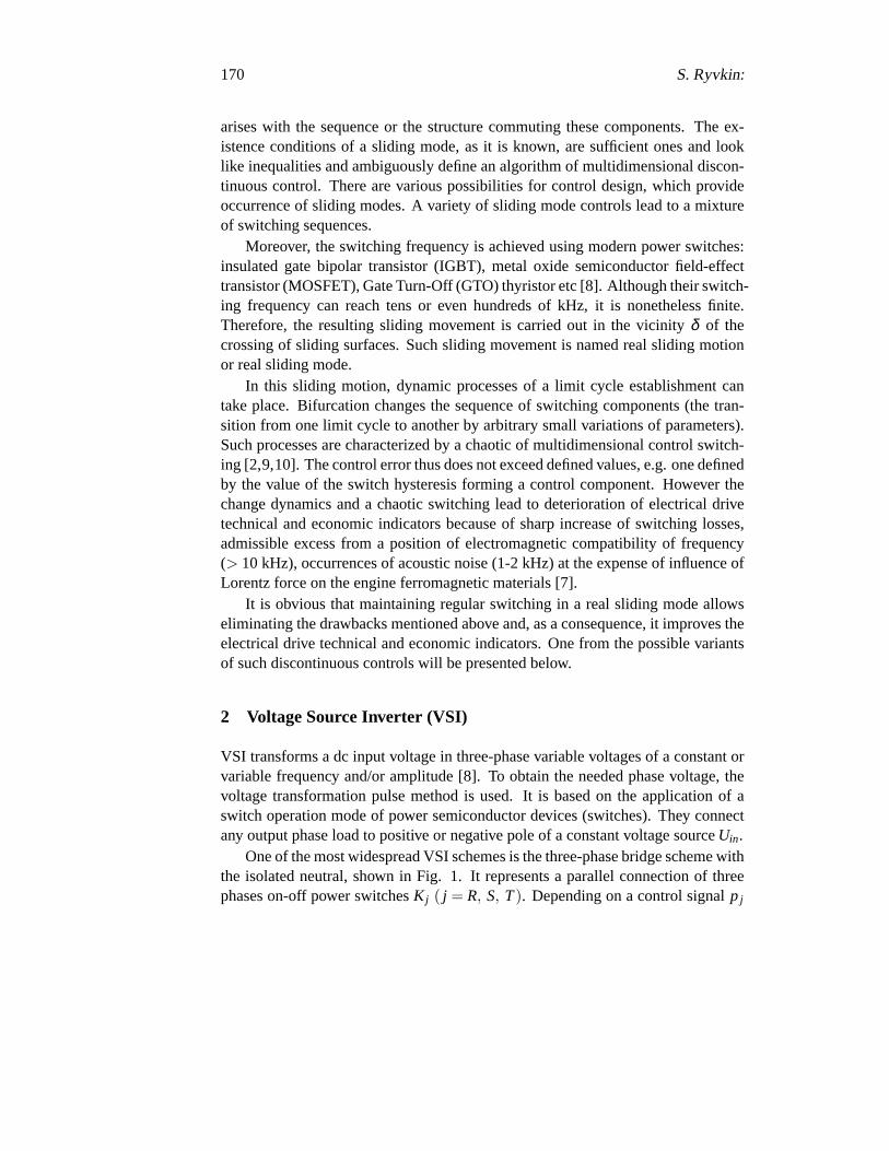
where numerical factors of a transformation matrix are directing the phase loadorts(R, S, T). As phase voltages have relay character the voltage output vector Ucan accept only seven values (Fig. 2): one of which is zeroU0, and other sixUk
(k= 1, . . . ,6) are not zero and also are the tops of the correct hexagon. Its symmetryaxes are directed on the phase load orts.
The module of the above mentioned six nonzero vectors depends on the loadconnection circuit and the value of the input dc line voltageUin. In the load, con-nected as ”star” circuit, it is equal to 2Uin/3. The combinations of phase switches(pR, pS, pT) controls are near the possible vectors of the output voltage Uk pre-sented in Fig. 2. A zero vector corresponds to two combinations of the switchpositions: either all are connected to positive potential (111), or to negative poten-tial (000).
172 S. Ryvkin:
•
•
•
•
• • α
β
U2(1 1 0)U3(0 1 0)
U6(1 0 1)U5(0 0 1)
U1(1 0 0)U4(0 1 1)U0
(0 0 0)
(1 1 1)
Fig. 2. Vectors of VSI momentary output.
3 VSI Control Design
From the viewpoint of noise abating, the regular switching of VSI switches consist-ing in cyclic transitions between the nearest vectors of VSI instant output voltage(Fig. 2) is quite attractive. Such law leads to serial switching of VSI phase switches,and the switching sequence remains invariable by all values of an average(duringmodulation period) voltage vector.
The control design problem consists in working out control of such commandsfor the VSI phase switches, that provide the regulation and desired (in agreementwith Fig. 2) character of the VSI instant output voltage vectors switching in realsliding movement.
When implementing a particular vector of instantaneous voltage, a change ofdirection of the current (or, in the quasi-static mode, at a relatively slow pacedsetting the current direction of change in the current implementation errors), de-termined by the difference vectors of instantaneous voltage and averagevoltagevector. The selecting criterion for the boundaries of switch control is desirableprocess of occurrence of real sliding mode, i.e. the process of establishing the se-quence and the modulation period for arbitrary initial values of the currenterrorvector.
That dynamic process of establishing the limit cycle characterizing the realsliding mode occupies a finit time and comes to an end for the final number ofswitching power switches. It is necessary that that border areas coincide with thetrajectories realized in real sliding mode.
The power switching function of each VSI phase is characterized by symmetric
VSI Sliding Mode Control with Regular Multidimensional Switching 173
“hysteresis” by small values of the VSI output voltage vector (Fig.3).
Fig. 3. Limit cycle for small values ofUeq.
In contrast to the relay phase current regulator in the vector control, theinputof the hysteresis element of each phase receives no error in the current phase, but alinear combination of the current phase errors.
In a central current error area (neighborhood of the zero current error point) dueto hysteresis remain the former values of instant voltage vector control (thecontrolcommand combinations (000) and (111), corresponding to VSI output zero voltageare forbidden). This form of a limiting cycle in the current error space differedfrom a correct hexagon by big values of a VSI output average voltagevector (nearthe maximal value).
As concluded from Fig. 3, the essence of the offered design approach of thevector relay tracking system consists in the formation of control switching areasborders in the current error space. These border directions coincide with ones ofthe difference between the VSI instant voltage vector and the average one, andthey are apart by an equal distance from the origin of coordinates. (This distanceis the parameter defining the switching frequency). In this case the realizationduration of any instant voltage vector in a cycle is not equal to zero. Thus, the samesequence commuting always remains. It is true, if the average voltage vector doesnot overstep the bounds of the realized voltage vector area.
The offered approach allows designing VSI power switch control for the currentclosed loop, which is presented below.
174 S. Ryvkin:
Let us define directing vectors of area borders:
E1 =
√
23
Uin(0,−1)T − (Ueqβ ,−Ueqα)T ,
E2 =
√
23
Uin(
√3
2,−1
2)T − (Ueqβ ,−Ueqα)T ,
E3 =
√
23
Uin(
√3
2,12)T − (Ueqβ ,−Ueqα)T ,
E4 =
√
23
Uin(0,1)T − (Ueqβ ,−Ueqα)T ,
E5 =
√
23
Uin(−√
32
,12)T − (Ueqβ ,−Ueqα)T ,
E6 =
√
23
Uin(−√
32
,−12)T − (Ueqβ ,−Ueqα)T ,
(2)
It is accepted that the characterizing switching surface by a directing ortei
(i = 1, . . . ,6) is orthogonal to the surface (line). To do this, normalize the previousexpressions (2) by dividing them by the absolute value of the orthogonalswitchingsurface vector,ei = Ei/ mod(Ei). Each surface is separated from the origin in thecurrent error space at an equal distance, denoted by the distance symbol δ (Fig.4).
Fig. 4. Formation of the switching surface.
The switching functionsi is formed as the inner product of the current errorvector∆i = (∆iα ,∆iβ ) and the directing ortei (i.e. the∆i projection and the direct-ing ort), with the additive componentδ , characterizing the distance between theswitching surface and the origin:
si = (∆i,ei)−δ = ∆iαeiα +∆iβ eiβ −δ . (3)
VSI Sliding Mode Control with Regular Multidimensional Switching 175
To obtain theδ estimation let us consider a switching cycle for small values ofthe average voltage vector(Ueq= 0). The cycle consists of six motions, the distancemoved by the current error vector for each motion is 2δ/
√3, and the speed of the
current error vector is equal to√
2/3Uin.Therefore, the cycle durationT is T = 12δ/
√2Uin. Hence, by a reference value
of T, the corresponding valueδ is determined by
δ = TUin
√2
12(4)
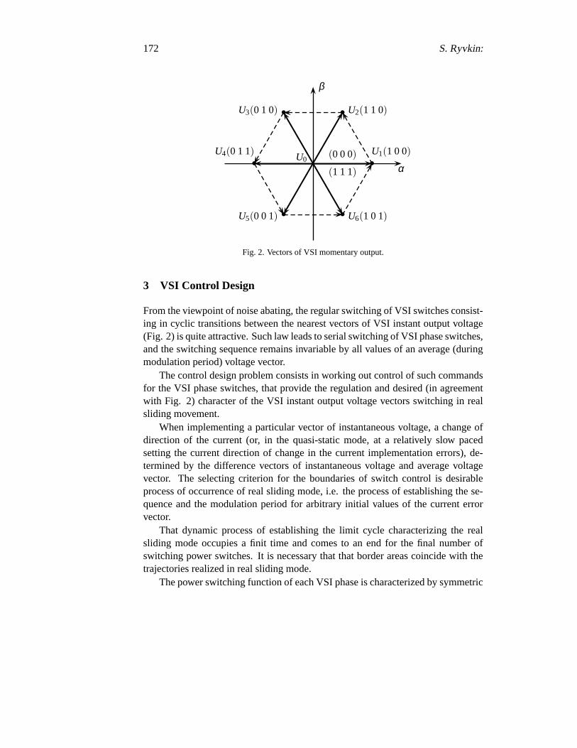
The base method of the control switching area borders formation in real slidingmovement is described above. We assume now that the switching functions sg(si)are generated. According to relay control the signs of these functions (logic signals)in the area must be defined. Required space splitting is defined by crossingthecontrol area borders. The desired partition in sectors is given by the intersection oftwo neighboring borders of switching control, and the sign of the logical functionof one of them is equal to ”1” and the other to ”0”. Possible combinations of logic(sign) functions(sg(s1), . . . ,sg(s6)) for these sectors and sector numbers are shownin Fig. 5 (the values of sign functions that do not influence on the area selection aremarked with an asterisk(∗)).
Fig. 5. Signs combinations of control switching functions.
E.g., the current error vector is in the sector 5. As shown the Fig. 4 the signsof the switching functionss4 ands5, i.e. sg(s4) = 0, sg(s5) = 1, define clearly thevector position in this sector, then the signs of the other switching functions in thissector are arbitrary (may be equal to 0 and 1, depending on the position ofthe affixin a particular area in this sector). In sector 1 sg(s1) = 1, sg(s2) = 0, and the signsof the other four switching functions can be equal to “1” or “0”.
These examples show that in general, to determine the sector in which the cur-rent control error vector is, it is necessary to use the values of two (out of six)
176 S. Ryvkin:
switching functions. The combination of characters is uniquely determined bythesector of the current error vector.
So, if the affix is in one of six sectors out of the area near the origin of co-ordinates possible combinations of switching functions signs are characterized bythe sequence of the values ”1” going successively (with cyclic shift), and “0”, alsogoing successively. The position of last “1” in sequence defines the sector number.However, such control structure is fair only by ”the correct” sector organization,when crossing their borders defines the convex hexagon that is a limit cycle trajec-tory of current error changing. In the presence of uncorrelated noise in switchingfunction signals, the “correct” control structure of the switching functions can bebroken, and an unequivocal definition of sector on the base of two correspondingswitching function signs is impossible. In such cases it is necessary to workout thespecial measures preventing “false” appointments of VSI switch controls.
Control selection should satisfy the following conditions:
• It should provide the desired limit cycle, i.e. the sequential switching of VSIpower switches phases.
• A hitting of the image point on the limit switching cycle should be providedfrom random initial conditions, as well as any changes of the current valueof the current error (accidental, caused by noise measurements, or animple-mentation error, or caused by changes of the current value of the reference).
• The hitting should occur within a finite time and finite number of powerswitchings.
The important condition is also noise immunity of this follow-up control plant:presence of noise in input signals of the comparators defining of switchingfunc-tion signs should not lead to changes of VSI switch control commands, at least bysmall enough noise level. Therefore control selection cannot be unequivocal (onall phases) by an accessory of a current error vector to this or that sector. The pres-ence of inevitable discrepancies and noise by the current measurement could leadto instant (with noise frequency) to switch control command changing. There isa necessity using additional ”hysteresis” in the control loop for ”cutting” noise ofmeasurement noises with small amplitudes.
Using “hysteresis” assumes the presence of VSI control command memory orswitching function memory and implementation of additional conditions of controlcommand selecting similar to switching device hysteresis forming by the scalarrelay control. It is convenient to realize hysteresis in vector follow-up control plantby using VSI control command memory. The control shown in Fig. 6 satisfies theseconditions.
In Fig.6 use of bold type indicates VSI(R, S, T) switch control command phases:1 - to switch-on the line(+), 0 - to switch-on line(−) of a direct current link. The
VSI Sliding Mode Control with Regular Multidimensional Switching 177
Fig. 6. Phase switching control command.
symbol(∗) means that the control command for this phase switch in this sector isnot defined. It could be 0 or 1, e.g. stored previous value. It is not defined in thecentral sector (retain their previous values). The control of all phases, however,control command combinations(0,0,0) or (1,1,1) are forbidden. It avoids the fre-quent change of phase control commands by the current error affix movement inthe neighborhood of any switching control boundary (“vector” hysteresis).
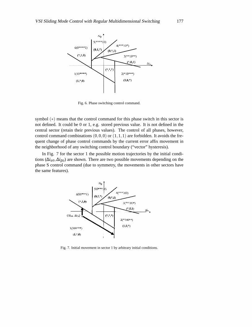
In Fig. 7 for the sector 1 the possible motion trajectories by the initial condi-tions (∆iα0,∆iβ0) are shown. There are two possible movements depending on thephase S control command (due to symmetry, the movements in other sectors havethe same features).
Fig. 7. Initial movement in sector 1 by arbitrary initial conditions.
178 S. Ryvkin:
4 Simplified Control
Switching functions (3) were defined earlier as scalar products of a current errorvector and a directing ort of the corresponding area border. However for controldesign only logic (sign) values of this switching functions sg(si) are used. Obvi-ously, the function signsi will not change, if it is multiplied by a positive numberequal to mod(Ei). Thus, the switching function assumes the following form:
si =(∆iαeiα +∆iβ eiβ ) mod(Ei)−δ mod(Ei)
=(∆iαEiα +∆iβ Eiβ )−δ mod(Ei)(5)
The first term in the equation (5) after substitution of variableEi , could berewritten in the form of the sum of scalar product of a current error vector andthe directing vectors defining directions of VSI output instant voltage vectors andscalar product of a current error vector and average voltage vector:
∆iαEiβ +∆iαEiβ = ∆iαUiα −∆iβUiα −∆iαUeqβ +∆iβUeqα
=
√
23
Uin(∆iαeiβ −∆iβ eiα)−∆iαUeqβ +∆iβUeqα(6)
Since the components of direction instant voltage vectorsei are predeterminedand known, the coefficients before the current error components of the current error∆iα , ∆iβ in the first term can be calculated in advance. And for this term calcula-tion adders of current error components can be used. Scalar product of the errorcurrent vector and the average voltage vector can be calculated by using adders andtwo multiplying digital-analog converters (their digital inputs get slowly changingcomponents of average voltage; their analog inputs get current components). It isvery important that the same scalar product be used in calculations of all sixofswitching functionssi .
For the calculation of switching functions is also necessary to compute (in theprocessor) the values of distances between the switching surfaces andthe origin ofcoordinate, i.e. the module of the difference between the instant voltage vectorsand the average one). It is useful to make a valuation of switching functions bycompleting the multiplication by
√
2/3Uin in the processor part to simplify thehardware.
5 Follow-up current vector control structure
Hardware implementation of vector relay control included a built-in an energy-efficient VSI control. Vector control was has not been widely used mainlydue tothe complexity of setting up this control, but there still remains an urgent design
VSI Sliding Mode Control with Regular Multidimensional Switching 179
problem of an electrical drive with digital, software-implemented system of relay-vector control. Such drive would have robustness to the changing semiconductorpower converter parameters, with the existing physical constraints of speed, as wellas the known advantages of digital control systems, namely: self-testing, auto-tuning, wide front-end and other features.
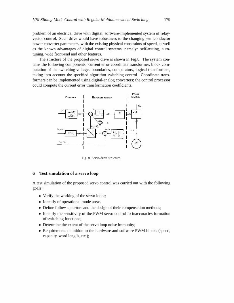
The structure of the proposed servo drive is shown in Fig.8. The systemcon-tains the following components: current error coordinate transformer, block com-putation of the switching voltages boundaries, comparators, logical transformers,taking into account the specified algorithm switching control. Coordinate trans-formers can be implemented using digital-analog converters; the control processorcould compute the current error transformation coefficients.
Fig. 8. Servo drive structure.
6 Test simulation of a servo loop
A test simulation of the proposed servo control was carried out with the followinggoals:
• Verify the working of the servo loop;;
• Identify of operational mode areas;
• Define follow-up errors and the design of their compensation methods;
• Identify the sensitivity of the PWM servo control to inaccuracies formationof switching functions;
• Determine the extent of the servo loop noise immunity;
• Requirements definition to the hardware and software PWM blocks (speed,capacity, word length, etc.);
180 S. Ryvkin:
• Identify possibilities to simplify the hardware;
• Develop proposals for implementing the servo PWM control.
Regarding the use of the servo PWM control in electrical drives, it should benoted that the feed back PWM, or the VSI with a close loop PWM that could benamed controlled current source, is aimed for use in fairly complex driveswithvector control. Electrical drive structure is not important by the PWM control sim-ulation. So it makes sense to conduct simulations for a simplified scheme of thepower unit, reflecting substantial (for a closed loop PWM control design)featuresof the VSI load. Such simplification may be in the representation of VSI three-phase load as two-dimensional one (in the generalized system) and an inductiveload connected in series with it, and a voltage source with two independent com-ponents. The values of the latter are exactly the values of the components oftheequivalent voltage.
This load is connected in series with a voltage source with two independentcomponents. Their values are exactly the values of the components of the equiv-alent voltage. In real electrical drives, the values of fundamental frequency of theVSI output voltages and of the PWM frequency are selected (tens to hundreds ofHz for the first and the units-tens of kHz for the second). It allows by simulationto use a constant (quasi-statically varying) voltage source in the VSI load,as wellas constant (quasi-statically changing) current component references for the closedloop PWM control. These assumptions allow closing the PWM loop without takinginto account the specifically features of the used motor.
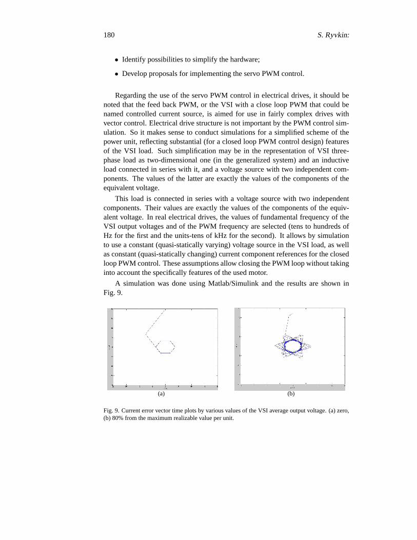
A simulation was done using Matlab/Simulink and the results are shown inFig. 9.
(a) (b)
Fig. 9. Current error vector time plots by various values of the VSI average output voltage. (a) zero,(b) 80% from the maximum realizable value per unit.
VSI Sliding Mode Control with Regular Multidimensional Switching 181
The presented current error vector time plots show that the suggested switchcontrol provides regular structure of VSI phase serial switching and itis not depen-dent on the average value of the VSI output voltage vector. Also, by the small val-ues of a VSI output average voltage, thanks to symmetric ”hysteresis” of the switch-ing functions of each VSI phase power switch a limit cycle of self-oscillations, i.e.a correct hexagon has been established at once. In contraposition to it,large VSIoutput average voltage values of the switching function (3) differ from symmetrichysteresis. The process of establishing a limit cycle is extended, and the limit cyclediffers a little from a correct hexagon.
7 Conclusions
It has been shown that there is a possibility of eliminating one of the disadvan-tages of the real sliding mode control: a chaotic switching of multidimensionalcontrol components.. It is a source of deterioration of electrical drive technicaland economic indicators because of sharp increase of switching losses,admissibleexcess from a position of electromagnetic compatibility of frequency (> 10 kHz),occurrences of acoustic noise (1-2 kHz). The maintaining regular switching in realsliding mode is provided with using the special switching lines. The original VSIcontrol integrates all merits of sliding mode control: a good dynamics behaviorandreducing of the influence of disturbances, and a merit of the fixed switching fre-quency. The commutation and modulation laws for each switch are automaticallyserving in real sliding mode. The possible hardware implementation is presented.The simulation confirms a regular structure of VSI phase serial switching that isnot dependent on the average value of the VSI output voltage vector.
References
[1] G. S. Buja and M. P. Kazmierkowski, “Direct torque control of PWM inverter-fedAC motor - a survey,”IEEE Trans. Ind. Electron, vol. 51, pp. 744–757, 2004.
[2] C. Lascu, I. Boldea, and F. Blaabjerg, “Variable-structure direct torque control - aclass of fast and robust controllers for induction machine drive,” IEEE Trans. Ind.Electron., vol. 51, pp. 785– 792, 2004.
[3] S. Ryvkin, “Sliding mode technique for ac drive,” inProc. 10th Int. Power Electron.& Motion Control Conf., EPE - PEMC 2002, Dubrovnik & Cavtat, Croatia, Sept.2002.
[4] A. Sabanovic, K. Jezernik, and N. Sabanovic, “Sliding mode applications in powerelectronics and electrical drives,” inVariable Structure Systems: Towards the 21 Cen-tury. Berlin, Germany: Springer - Verlag, 2002, pp. 223 –252.
[5] V. Utkin, J. Shi, and J. Gulder,Sliding modes in electromechanical systems. London,UK: Taylor & Francis, 1999.
[6] J. Vittek and S. J. Dodds,Forced dynamics control of electric drives. Zilina: EDIS- Publishing Center of Zilin University, 2003.
182 S. Ryvkin:
[7] J. Holz, “Pulsewidth modulation for electronic power conversion,”IEE Proc., vol. 82,no. 8, pp. 1194–1213, 1994.
[8] N. Mohan, T. M. Underland, and W. P. Robbins,Power electronics: converters, ap-plications and design, 3rd ed. New York, USA: John Wiley & Son Inc., 2003.
[9] I. Nagy, “Improved current controller for PWM inverter drives with the backgroundof chaotic dynamics,” inProc. 20th Int. Conf. Ind. Electron., Control and Instrumen-tation, IECOM’94, Bologna, Italy, Sept. 1994, pp. 561–566.
[10] Z. Suetz, I. Nagy, L. Backhauz, and K. Zaban, “Controlling chaos in current forcedinduction motor,” inProc. 7th Int. Power Electron. & Motion Control Conference,PEMC’96, vol. 3, Budapest, Hungary, Sept. 1996, pp. 282–286.