Page 1
For PI Meeting distribution only, [email protected]
Waferscale Accelerators for High Energy Ions and Electrons
Amit Lal
School of Electrical and Computer Engineering
Cornell University
10/20/2013
ARPA-E Workshop on Fusion Drivers
Berkeley, CA
Page 2
For PI Meeting distribution only, [email protected]
• Electric fields for Ion Manipulation
• Fabrication process flow for wafer-scale accelerators
• Einzel Lens, LINAC
• CMOS Electronic Detection
• Conclusions
Outline
2
Page 3
For PI Meeting distribution only, [email protected]
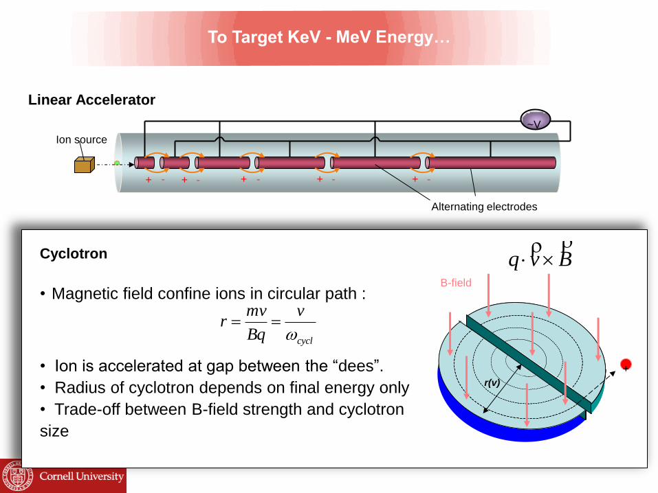
+ + + + + - - - - -
~V
Ion source
Alternating electrodes
B-field
+
Cyclotron
Linear Accelerator
• Magnetic field confine ions in circular path :
• Ion is accelerated at gap between the “dees”.
• Radius of cyclotron depends on final energy only
• Trade-off between B-field strength and cyclotron
size
cycl
v
Bq
mvr
r(v)
Bvq
Page 4
For PI Meeting distribution only, [email protected]
-
Vaccel
~ +
N
S
BvqFmagnetic
EqFelectric
Microtron
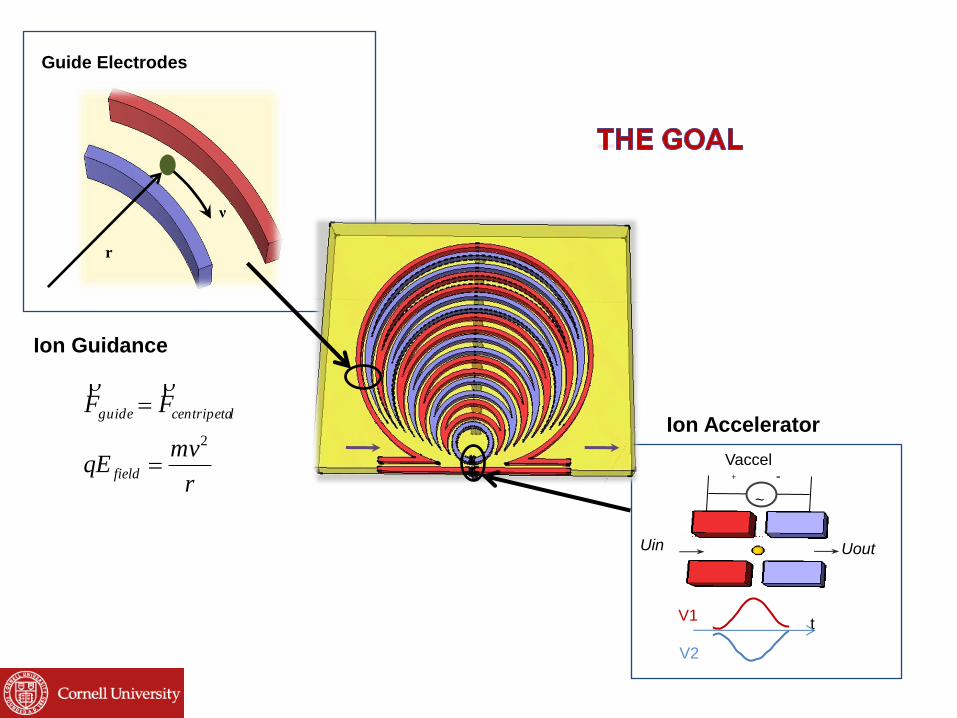
Guide
Electrodes
DC
Page 5
Guide Electrodes
r
ν
+ -
~
Vaccel
Uin Uout
V V1
V2
t
Ion Guidance
Ion Accelerator
r
mvqE
FF
field
lcentripetaguide
2
Page 6
For PI Meeting distribution only, [email protected]
Acce
lera
tion
30
0u
m
200um
Gu
ida
nce/e
nerg
y s
ele
cto
r 30um
Sensor electrode
Driven at 35MHz
Gap gain:20eV
Total gain: 60eV
1
2
3
4
Page 7
For PI Meeting distribution only, [email protected]
4
2
2
3
2
3
0
4
2
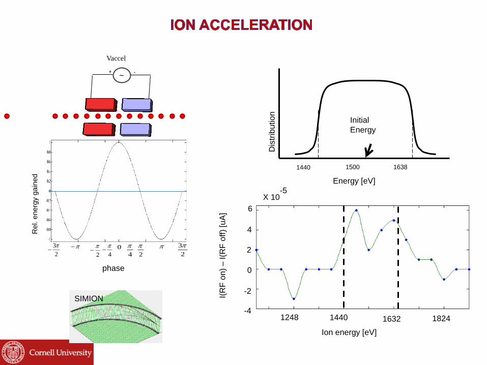
+ - ~
Vaccel
~
phase
Rel. e
nerg
y g
ain
ed
Initial
Energy
SIMION
1248 1440 1632 1824
Ion energy [eV]
-4
-2
0
2
4
6
X 10-5
I(R
F o
n)
– I(R
F o
ff)
[uA
]
1500 1638 1440
Energy [eV]
Dis
trib
utio
n
Page 8
For PI Meeting distribution only, [email protected]
• Electric fields for Ion Manipulation
• Fabrication process flow for wafer-scale accelerators
• Einzel Lens, LINAC
• CMOS Electronic Detection
• Conclusions
Outline
8
Page 9
For PI Meeting distribution only, [email protected]
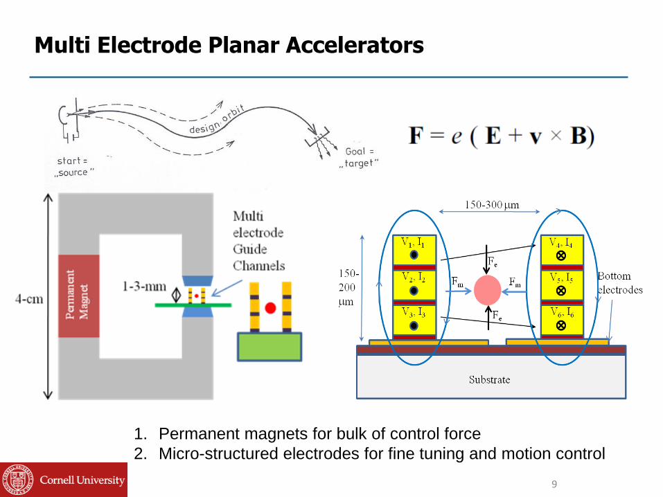
Multi Electrode Planar Accelerators
9
1. Permanent magnets for bulk of control force
2. Micro-structured electrodes for fine tuning and motion control
Page 10
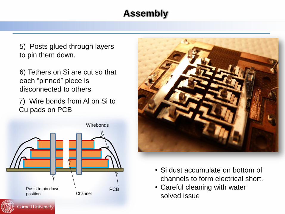
PCB
5) Posts glued through layers
to pin them down.
6) Tethers on Si are cut so that
each “pinned” piece is
disconnected to others
7) Wire bonds from Al on Si to
Cu pads on PCB
Posts to pin down
position Channel PCB
Wirebonds
• Si dust accumulate on bottom of
channels to form electrical short.
• Careful cleaning with water
solved issue
Assembly
Page 11
OPERA (June)
Consecutive Series of Einzel Lens
Page 12
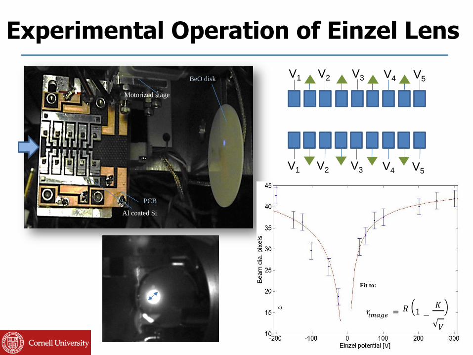
Experimental Operation of Einzel Lens
BeO disk
Motorized stage
PCB
Al coated Si
𝑟𝑖𝑚𝑎𝑔𝑒 = 𝑅 1 −𝐾
𝑉
Fit to:
c)
V1 V2 V3 V4 V5
V1 V2 V3 V4 V5
Page 13
- - + +
Coplanar Waveguide Resonator Accelerator
• RF gen. power = 50W
• Vdrive =10V (for 1000Ω)
• Q can be high ~ 500
• Va ~ 100kV
Amplifier
RF signal generator
Resonator
Wire bonds Linac
Page 14
FARHAN RANA: CORNELL SEMICONDUCTOR OPTOELECTRONICS GROUP
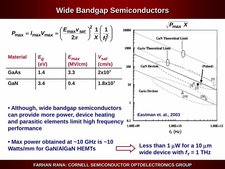
Wide Bandgap Semiconductors
2
2max
maxmaxmax11
2T
sat
fX
vEVIP
Material Eg
(eV)
Emax
(MV/cm)
Vsat
(cm/s)
GaAs 1.4 3.3 2x10⁷
GaN 3.4 0.4 1.8x10⁷
Eastman et. al., 2003
XPmax
HzTf
• Although, wide bandgap semiconductors
can provide more power, device heating
and parasitic elements limit high frequency
performance
• Max power obtained at ~10 GHz is ~10
Watts/mm for GaN/AlGaN HEMTs Less than 1 mW for a 10 mm
wide device with fT = 1 THz
Page 15
For PI Meeting distribution only, [email protected]
Design of Resonator Facilitated Linear Accelerator
Page 16
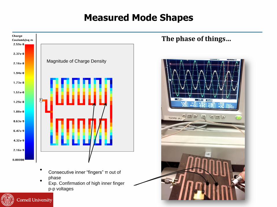
Magnitude of Charge Density
• Consecutive inner “fingers” π out of
phase • Exp. Confirmation of high inner finger
p-p voltages
The phase of things…
Measured Mode Shapes
Page 17
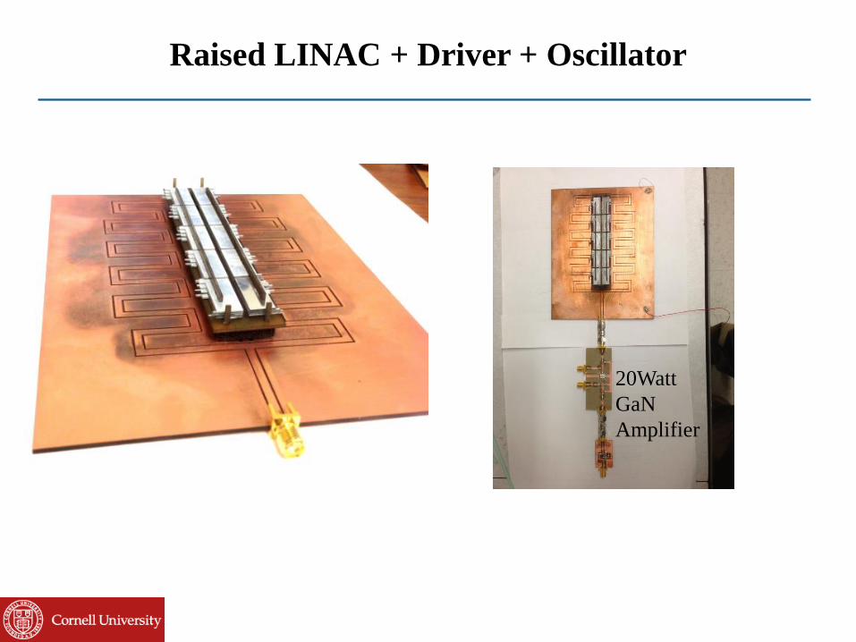
Raised LINAC + Driver + Oscillator
20Watt
GaN
Amplifier
Page 18
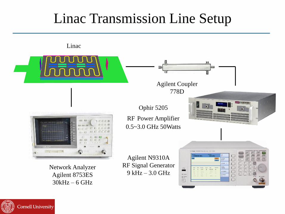
Linac Transmission Line Setup
Linac
Network Analyzer
Agilent 8753ES
30kHz – 6 GHz
Agilent Coupler
778D
Ophir 5205
RF Power Amplifier
0.5~3.0 GHz 50Watts
Agilent N9310A
RF Signal Generator
9 kHz – 3.0 GHz
Page 19
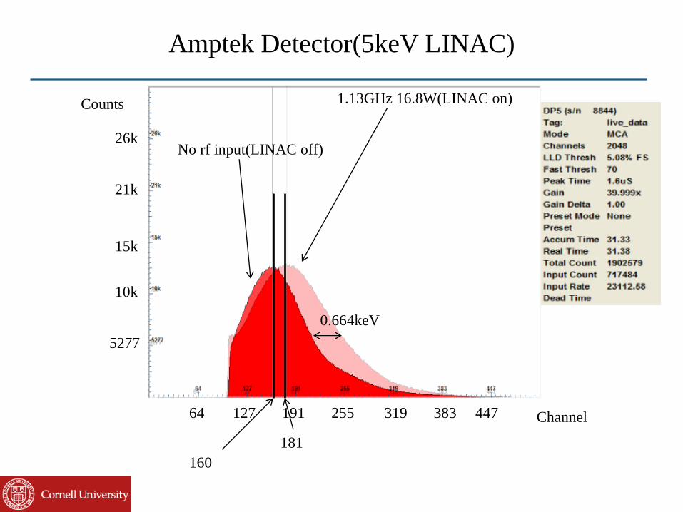
Amptek Detector(5keV LINAC)
No rf input(LINAC off)
1.13GHz 16.8W(LINAC on) Counts
5277
10k
15k
21k
Channel 64 127 191 255 319 383 447
26k
181
160
0.664keV
Page 20
For PI Meeting distribution only, [email protected]
• Electric fields for Ion Manipulation
• Fabrication process flow for wafer-scale accelerators
• Einzel Lens, LINAC
• CMOS Electronic Detection
• Conclusions
Outline
20
Page 21
For PI Meeting distribution only, [email protected]
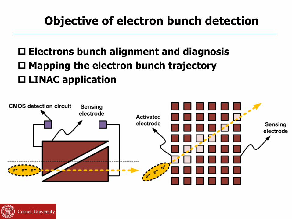
Electrons bunch alignment and diagnosis
Mapping the electron bunch trajectory
LINAC application
Objective of electron bunch detection
Page 22
Sensor Electronics
22
)()( 22121 nvnsignalvvout vAvvAAv
ox
density
ox
density
signalC
q
AC
Aqv
Exposed pad for charge-sensing
Conn. to buried transistors with vias and
intermediate metal layers
Input transistor for charge
to voltage conversion
• Ratio of sensed charge to capacitance i.e. measured
voltage is fixed for given charge concentration •Amplifier with large (~40 dB) gain used for measuring
voltage generated by sensed charge • Input-referred noise of amplifier competes with signal
i.e. it must be suppressed to detect ion-charges. This is
dominated by input transistor so can ignore vn2
Capacitance to substrate that
computes voltage from charge
HzVg
kTv
m
n /4 2
1
Page 23
For PI Meeting distribution only, [email protected]
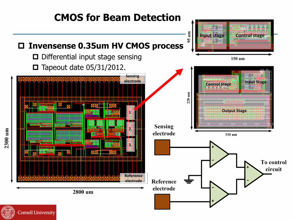
Invensense 0.35um HV CMOS process
Differential input stage sensing
Tapeout date 05/31/2012.
CMOS for Beam Detection
Page 24
For PI Meeting distribution only, [email protected]
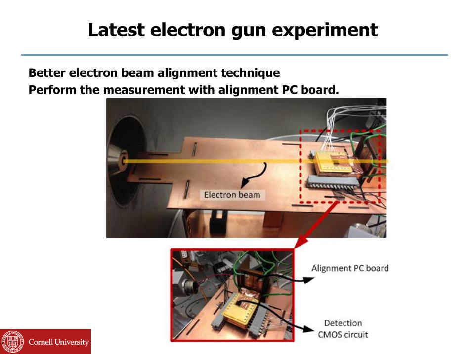
Better electron beam alignment technique
Perform the measurement with alignment PC board.
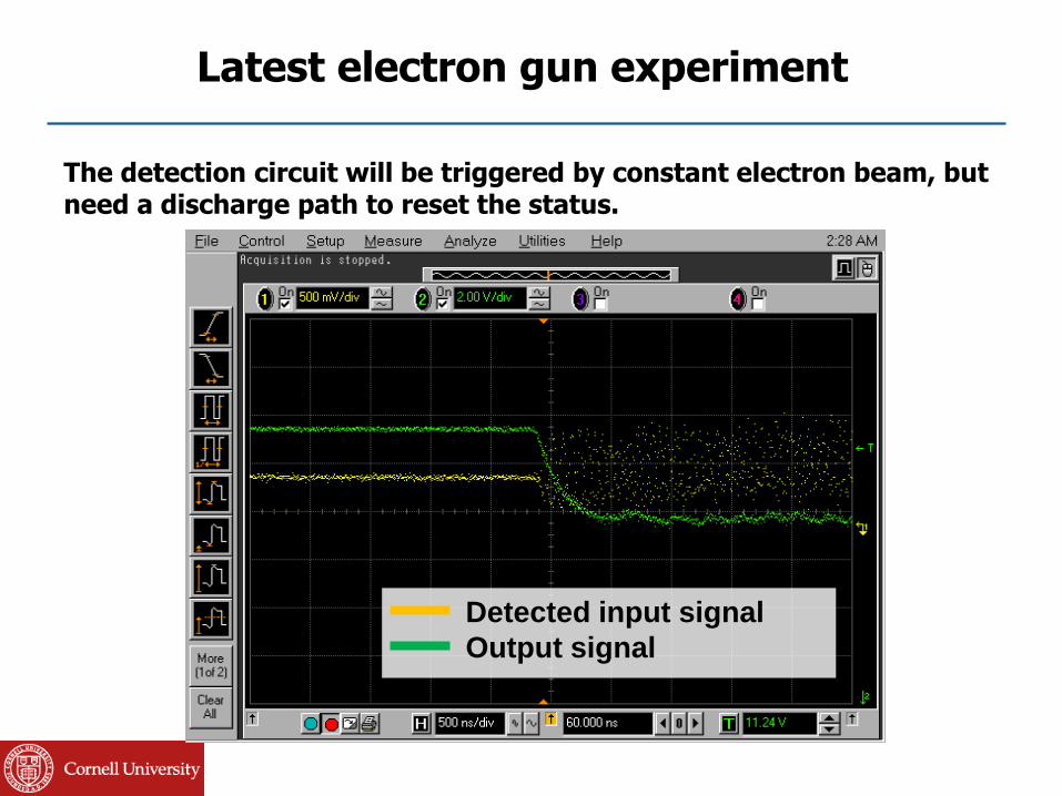
Latest electron gun experiment
Page 25
For PI Meeting distribution only, [email protected]
The detection circuit will be triggered by constant electron beam, but need a discharge path to reset the status.
Latest electron gun experiment
Detected input signal
Output signal
Page 26
[email protected]
Fusion Ion Beam – Potential Design
26
Page 27
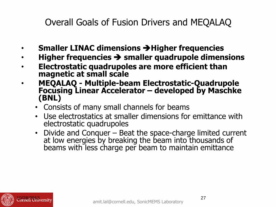
Overall Goals of Fusion Drivers and MEQALAQ
• Smaller LINAC dimensions Higher frequencies • Higher frequencies smaller quadrupole dimensions
• Electrostatic quadrupoles are more efficient than magnetic at small scale
• MEQALAQ - Multiple-beam Electrostatic-Quadrupole Focusing Linear Accelerator – developed by Maschke (BNL)
• Consists of many small channels for beams • Use electrostatics at smaller dimensions for emittance with
electrostatic quadrupoles • Divide and Conquer – Beat the space-charge limited current
at low energies by breaking the beam into thousands of beams with less charge per beam to maintain emittance
10/28/2013 [email protected] , SonicMEMS Laboratory
27
Page 28
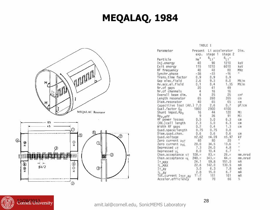
MEQALAQ, 1984
10/28/2013 [email protected] , SonicMEMS Laboratory
28
Page 29
What does MEMS offer?
• Very high smoothness => minimize field emission (Silicon wafers are ~ 2-10nm surface roughness)
• Small drift-tubes can be made in arbitrary patterns using lithography and plasma etching
• Integrated electrostatic actuators to align beam alignment and change function of electrostatic beam manipulators
10/28/2013 [email protected] , SonicMEMS Laboratory
29
Page 30
Integrated Actuators with JFET transistors
30 SonicMEMS
L A B O R A T O R Y
Page 31
Movable Quadrupole Electrodes
31 SonicMEMS
L A B O R A T O R Y
Page 32
4-inch wafer
Holder with RF CPW
resonator GaN RF amplifier –
50W
• Q ~ 700, Z0 = 200 Ohms, P = 50 W = > Peak
voltage = 100kV • Heat removal at 50W/5cm
2
• RF design for equal phase at each beam
channel • Each wafer has its own resonator
Silicon Wafer Held By CPW Resonator: MEMS MEQALAQ
10/28/2013 [email protected] , SonicMEMS Laboratory
32
Page 33
Very Crude Cost Analysis
• Per accelerator wafer
• Amplifier/Power Amplifier - $3
• Wafer ~ $5
• Processing ~$10
• CPW Resonator ~ $1
• Vacuum chamber ~$1
• Total ~ $20/wafer in large quantities
• Assuming 8000 channels per wafer, and 20,000 wafers to get to 2 GeV 200 amu ions
• 200 meter long
• $400K /accelerator at 400 Amps
• 100kA => 250 accelerators => $100M
10/28/2013 [email protected] , SonicMEMS Laboratory
33
Page 34
Summary
• Micromachining and MEMS enables electrostatic quadrupoles at massive densities and low cost due to economies of scale per wafer
• Distributed amplifiers may enable distributed heat dissipation
• Economies of scale of Moore’s law maybe applied for low-cost fusion drivers
34