Page 1
Supporting Information
Waterproof perovskite-hexagonal boron nitride hybrid
nanolasers with low lasing thresholds and high operating
temperature
Haoran Yu, Xing Cheng, Yang Liu, Kexiu Rong, Yilun Wang, Ziling Li, Yi Wan,
Wenting Gong, Kenji Watanabe, Takashi Taniguchi, Shufeng Wang, Jianjun Chen, Yu
Ye* and Lun Dai*
*Corresponding authors, E-mails: [email protected] , [email protected]
Section 1. Growth of CsPbI3 nanoplates (NPs) via chemical vapor deposition
(CVD) method
Schematic diagram illustrates the experimental setup of our home-built CVD system
(Figure S1a), and optical image of the typically synthesized CsPbI3 NPs show regular
rectangle shapes as well as smooth surfaces (Figure S1b). Due to the interference
effect between the top and bottom facets, the CsPbI3 NPs with different thicknesses
show different colors.
Page 2
Figure S1. CVD growth of CsPbI3 NPs. (a) Schematic diagram of the CVD
experimental setup. (b) Optical image of the representative CsPbI3 NPs grown on
muscovite mica substrate. Scale bar: 10 μm.
Section 2. Transfer of hBN capping layer
In order to see the influence of hBN capping on the lasing performance of CsPbI3 NP,
characterization of the pump intensity dependent emission spectra is firstly conducted
on the bare NP (Figure S2a). Afterwards, the hBN capping layer is transferred using
the dry transfer method under the help of a micromanipulator (Figure S2b).1 Firstly,
the hBN flakes are mechanically exfoliated on the viscoelastic PDMS stamp, adhering
to a glass slide. Then, an hBN with proper size and thickness (indicated by its optical
contrast) is selected under the optical microscope. Later, the hBN flake and the
selected NP are aligned under the microscope. The PDMS stamp needs to be pressed
against the target substrate slowly to achieve a bubble-free contact. Finally, the PDMS
stamp is slowly peeled off from the substrate, leaving the hBN capping layer on top of
the CsPbI3 NP (Figure S2c).2 After that, the second pump intensity dependent
Page 3
emission spectra measurement is conducted on the hBN capped CsPbI3 NP.
Figure S2. Transfer of hBN capping layer onto CsPbI3 NP. (a) Optical image of the
bare CsPbI3 NP on muscovite mica, which is used for lasing characterization before
hBN capping. (b) Diagrams of the deterministic transfer steps of the hBN capping
layer. (c) Optical image of the hBN capped CsPbI3 NP, which is used for lasing
characterization after hBN capping. Length of the scale bars in both a and c is 10 μm.
Section 3. AFM characterizations of the hybrid structure
Using atomic force microscopy (AFM), the topography of the CsPbI3 NP-hBN hybrid
structure is measured (Figure S3a). The height profile along the white dashed line
gives the thicknesses of CsPbI3 NP and hBN flake to be about 177 nm and 57 nm,
respectively (Figure S3b).
Page 4
Figure S3. AFM characterizations of the hybrid structure. (a) The topography of the
CsPbI3 NP-hBN hybrid structure measured by AFM. (b) Cross section profile of
height variation along the white dashed line in a.
Section 4. Three-dimensional simulation of WGM electric field distribution
We simulate the three-dimensional electric field distribution of the CsPbI3 NP-hBN
hybrid structure. The dimensional parameters of the hybrid structure are duplicated
from the AFM measurement. Refractive indices of hBN flake, CsPbI3 NP and
muscovite mica substrate are 2.173, 3.284 and 1.58, respectively. The planforms along
z-axis and x-axis (Figure S4) indicate that it is transverse electric (TE with the electric
field component parallel to the surface of CsPbI3 NP) whispering gallery mode
(WGM) supported by the hBN capped CsPbI3 NP.
Page 5
Figure S4. Simulated three-dimensional electric field distribution of the CsPbI3 NP
after hBN capping.
Section 5. Optical images and polarization-dependent emission of the NP above
lasing threshold
The sharp increase of output intensity (‘kink’ behavior in L-L curves) and the sudden
reduction in full-width at half-maximum (FWHM) have confirmed the formation of
high quality WGM nanolaser. To further characterize lasing operation, we take optical
images of the far-field radiation pattern and measure the polarization of the lasing
emission.
Page 6
Figure S5. Optical images of the CsPbI3 NP’s emission. (a) and (b), Optical images
of the far-field radiation pattern from CsPbI3 NP under pump intensity below and
above lasing threshold, respectively. Length of the scale bars in both a and b is 5 μm.
Optical image of the emission below lasing threshold shows uniform spontaneous
emission over the whole CsPbI3 NP (Figure S5a). Above threshold, strong emissions
are observed at the four corners, due to the sharp geometry change. In addition, there
exist clear interference fringes (Figure S5b), indicating the coherent light emission.
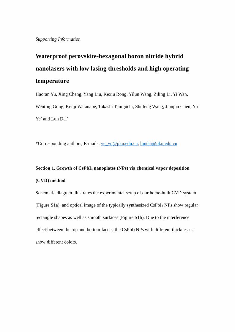
For the measurement of the polarization-dependent lasing intensity of the CsPbI3 NP,
we use a linear polarizer, and a pinhole (~500 μm) placed at the image plane to
achieve the spatial resolution of ~2.5 μm. We selectively collect the scattering light of
the lasing emission at different positions from a CsPbI3 NP (5.06 μm×5.07 μm, see
Figure S6a), including a corner of the NP (point A) and a midpoint of an edge (point
B). The intensity of the lasing peak (Figure S6b for point A; Figure S6c for point B)
shows strong polarization dependence. However, the degree of linear polarization is
limited by the size of the pinhole, since the scattering light from different positions
show distinct polarizations.
Page 7
Figure S6. Polarization-dependent emission of the NP above lasing threshold. (a)
Lasing emission image of the measured NP. The measured points A and B are marked
by dashed circles. (b) and (c), The measured polarization-dependent lasing intensities
at points A and B, respectively.
Section 6. FWHM of the resonant peak above lasing threshold before and after
hBN capping of the NP nanolasers
Lasing emission spectra of CsPbI3 NP taken under identical pump intensity above
lasing threshold (375.44 μJ/cm2) before (Figure S7a) and after (Figure S7b) hBN
capping are fitted by two Gaussian functions. The FWHM (Δλ) of the resonant peak
above the lasing threshold increases from 0.63 nm to 1.17 nm after hBN capping.
Page 8
Figure S7. Fitting of the spectrum before and after hBN capping. (a) Emission
spectrum of CsPbI3 NP before hBN capping. The FWHM of the resonant peak is 0.63
nm. (b) Emission spectrum of CsPbI3 NP after hBN capping The FWHM of the
resonant peak is 1.17 nm.
Section 7. Rate equation analysis
In order to further investigate the influence of hBN capping, we obtain the
spontaneous emission factor, β, of the nanolaser using rate equation analysis.5-7 The
dynamics of the excited electronic state population n and photon number s that couple
into a specific lasing mode can be represented as the following equations:
d𝑛𝑛d𝑡𝑡
= 𝑝𝑝 − 𝐴𝐴𝐴𝐴 − 𝛽𝛽Γ𝐴𝐴𝐴𝐴(𝐴𝐴 − 𝐴𝐴0) (1)
d𝑠𝑠d𝑡𝑡
= 𝛽𝛽𝐴𝐴𝐴𝐴 + 𝛽𝛽Γ𝐴𝐴𝐴𝐴(𝐴𝐴 − 𝐴𝐴0) − 𝛾𝛾𝐴𝐴 (2)
where p is a pumping rate, A is the total spontaneous emission rate into all modes, β is
the spontaneous emission factor, Γ is the optical confinement factor, n0 is the excited
state population at transparency, and γ is the total cavity mode loss rate. For simplicity,
we assume Γ to be one, and n0 to be zero. When it reaches steady state, both d𝐴𝐴 d𝑡𝑡⁄
Page 9
and d𝐴𝐴 d𝑡𝑡⁄ equal zero, which leads to the following relationship.
𝑝𝑝 = 1+𝛽𝛽𝑠𝑠𝛽𝛽(1+𝑠𝑠)
∙ 𝛾𝛾𝐴𝐴 (3)
We take the pump fluence intensity of the excitation as p, and the output intensity of
the oscillation peak as s. The experimental data can be best fitted with a spontaneous
emission factor, β, of 0.0203 (0.0163) before (after) hBN capping (Figure S8).
Figure S8. Curve fittings to the experimental data using rate equation analysis.
Section 8. TRPL measurements of another CsPbI3 NP
For further investigations about the dynamics of lasing in CsPbI3 NPs and the
influences of hBN capping, we conducted time-resolved photoluminescence (TRPL)
measurements using a 517 nm femtosecond laser over a time window of about 1.34 ns
on another CsPbI3 NP (Figure S9). The TRPL is measured four times for a CsPbI3 NP:
(a) excitation intensity below lasing threshold, before hBN capping; (b) excitation
intensity (identical to a) below lasing threshold, after hBN capping; (c) excitation
intensity above lasing threshold, before hBN capping; (d) excitation intensity
(identical to c) above lasing threshold, after hBN capping. Below lasing threshold, we
Page 10
perform mono-exponential fitting to the PL decay curve. Above lasing threshold, we
perform bi-exponential deconvolution fitting to the experimental data. Under low
pump intensity below lasing threshold, the spontaneous emission lifetime increases
from 729.9 ps to 859.2 ps after hBN capping (Figure S10a, b and c). Besides, there
exists a remarkable PL enhancement after hBN capping. Above the lasing threshold,
there is a new fast decay component appears both before (27.20 ps, 85.01%) and after
(28.92 ps, 79.25%) hBN capping, which decays more rapidly than the other
component (386.96 ps, 14.99% before hBN capping; 347.28 ps, 20.75% after hBN
capping, see Figure S10a, d and e). These results are consistent with the data
presented in the main text.
Figure S9. Optical images of another measured sample before and after hBN capping.
(a) Optical image of another CsPbI3 NP before hBN capping. (b) Optical image of the
CsPbI3 NP after hBN capping. Length of the scale bars in both a and b is 10 μm.
Page 11
Figure S10. Time-resolved photoluminescence (TRPL) measurements of another
sample. (a) Typical TRPL decay transients following photo-excitation of another
CsPbI3 NP with pump fluence below and above lasing threshold, before and after
hBN capping. The instrument response function is plotted with the gray dashed line.
(b-e) Images of spectrum vs. time (collected over a time window of about 1.34 ns)
taken under different conditions. (b) Below lasing threshold, before hBN capping; (c)
Below lasing threshold (with identical pump intensity as in B), after hBN capping; (d)
Above lasing threshold, before hBN capping; (e) Above lasing threshold (with
identical pump intensity as in d), after hBN capping.
Here we further analyze the reason behind PL enhancement. The phenomenological
lifetime 𝜏𝜏 depends on the radiative recombination lifetime 𝜏𝜏𝑟𝑟 and the total lifetime
resulted from different nonradiative recombination pathways 𝜏𝜏𝑛𝑛𝑟𝑟 as the following
equation:
𝜏𝜏−1 = 𝜏𝜏𝑟𝑟−1 + 𝜏𝜏𝑛𝑛𝑟𝑟−1 (4)
At room-temperature, since 𝜏𝜏𝑛𝑛𝑟𝑟 ≪ 𝜏𝜏𝑟𝑟 (PL quantum yield ~8.3%8), 𝜏𝜏 is
Page 12
approximately to be equal to 𝜏𝜏𝑛𝑛𝑟𝑟. The PLQY can be estimated by the ratio of radiative
rate to total rate as:
𝑃𝑃𝑃𝑃𝑃𝑃𝑃𝑃 =radiative rate
total rate ~
1𝜏𝜏𝑟𝑟
1𝜏𝜏𝑟𝑟
+ 1𝜏𝜏𝑛𝑛𝑟𝑟
=1
1 + 𝜏𝜏𝑟𝑟𝜏𝜏𝑛𝑛𝑟𝑟
(5)
With the surface passivation brought by hBN capping, surface traps induced
nonradiative recombination rate becomes slower, resulting a longer 𝜏𝜏𝑛𝑛𝑟𝑟, and
accordingly, higher PLQY, which leads to a higher PL emission intensity.
Section 9. Simulation of thermal dissipation
To demonstrate the efficient thermal dissipation induced by hBN capping, we
simulate the whole dissipation process within the first pump cycle, with an initial
temperature set to be 25 ℃ (for both of the device and the environment). To simplify
the calculation, we take the NP as a circular disk, since the shape of the sample will
not change the nature of thermal dissipation. In this way, a two-dimensional
axisymmetric model is set up. The dimension of the model’s geometry is close to the
actual size of the NP, i.e. the radius of the perovskite circular disk is 2.5 μm. The
boundaries are set at 15 μm (30 μm) away from the center of the disk in the vertical
(lateral) direction, which is far enough to be taken as infinity. Temperatures along the
boundaries keep constant at 25 ℃ during the simulation. The laser spot is large
enough (~ 21 μm) to cover the whole NP. So, the heating induced by nonradiative
recombination is approximately uniform in the CsPbI3 NP.9 We assume that the pump
power intensity is constant at 200 kW/cm2 during the 4.5 ns pulse duration. Since both
Page 13
hBN and mica are almost transparent, the absorption can be ignored. We assume that
the energy of the excitation photons will either be converted into the energy of the
emitted photons or into heat.
The relation between heating power intensity 𝑃𝑃ℎ and pump power intensity 𝑃𝑃𝑝𝑝= 200
kW/cm2, can be taken as:
𝑃𝑃ℎ = 𝑃𝑃𝑝𝑝 �1 − 𝑃𝑃𝑃𝑃𝑃𝑃𝑃𝑃 ∙ 𝜆𝜆𝑝𝑝𝜆𝜆𝐸𝐸� (6)
where PLQY is about 8.3% for CsPbI3 NP.8 λp = 532 nm and λE ~ 700 nm are the
wavelengths of excitation laser and the PL emission from the CsPbI3 NP, respectively.
Here, we assume the absorption to be approximately 100% (with absorption
coefficient α ≈ 1.5×105 cm−1 at 532 nm10 and CsPbI3 NP’s thickness of 177 nm). The
mesh for calculation and time steps are set to be identical for the CsPbI3 before and
after hBN capping.
Thicknesses of different layers are given in Figure S3b. The parameters of hBN
capping layer, CsPbI3 NP, and muscovite mica substrate are listed in Table S1. An
anisotropic thermal conductivity of hBN is applied, which is much higher than those
of the air and CsPbI3. Thus, the thermal dissipation is largely improved after hBN
capping, and the clear distinction can be seen in the main text (Figure 3a)
Page 14
The heat flux (at time of 50 ns) inside the structure before (Figure S11a) and after
(Figure S11b) hBN capping, with arrows depicting the magnitude and direction,
clearly shows that the heat dissipates mostly through hBN layer and more rapidly
after hBN capping. Before hBN capping, thermal dissipation is mainly through the
CsPbI3 crystal and mica substrate, since the thermal conductivity of air is very low.
There is a large portion of heat passing through the CsPbI3 NP, increasing the
temperature of the material. However, after hBN capping, heat flux is mostly confined
inside the highly anisotropic thermal conductive hBN layer, with the in-plane
component of the heat flux larger than the out-of-plane component. Since there exists
a new and effective pathway for thermal dissipation after hBN capping, heat conveyed
into the CsPbI3 NP is reduced enormously, leading to a slower temperature increase
and a faster cooling process inside the CsPbI3 NP.
Page 15
Figure S11. The heat flux (at time of 50 ns) inside the hybrid structure before and
after hBN capping. (a) Illustration of heat flux before hBN capping. (b) Illustration of
heat flux after hBN capping.
Section 10. More experimental results of lasing under high temperature
a. Lasing characterization under high temperature before and after hBN capping
of the same CsPbI3 NP
In order to further verify the effect of hBN capping on CsPbI3 NP lasing under high
temperature, we adopt two different samples. Both of them are measured before and
after hBN capping under identical excitation power range, with one sample measured
at 56.8 ℃ (Figure S12a) and the other measured at 60.7 ℃ (Figure S12b).
Figure S12. Lasing characterization under high temperature. (a) Normalized spectral
maps of a CsPbI3 NP before and after hBN capping measured at 56.8 ℃ under
identical excitation range. Before hBN capping, the sample can hardly lase. However,
Page 16
clear lasing behavior can be seen from the sample after it is covered by an hBN flake.
(b) Spectral maps of the other CsPbI3 NP before and after hBN capping measured at
60.7 ℃ under identical excitation range. The amplified spontaneous emission appears
in the sample, after it is covered by an hBN flake.
When the temperature is set at 56.8 ℃, we can see a clear comparison between the
two spectral maps measured before and after hBN capping (Figure S12a). Lasing
behavior is observable after hBN capping. It is noted that the bare CsPbI3 NPs without
hBN capping layer can be damaged by laser irradiation to some extent at high
temperature. These damages, appearing as dark spot on the CsPbI3 NP’s top surface,
can only be discerned in optical images after hBN capping. When the temperature
reaches 60.7 ℃, most of the samples are so badly damaged during the first
measurement before hBN capping, that the lasing behavior can be hardly observed
even after hBN capping (Figure S12b).
b. Temperature-dependent lasing characterization with hBN capping
In the main text, the experiments about lasing under high temperature are done on a
selected sample from the previously measured sixteen ones. In the optical image after
hBN capping, no clear damage is found. In this case, a clear lasing behavior at 75.6 ℃
can be observed.
c. Failure of observation of lasing in three bare CsPbI3 NP at 60 °C
Page 17
Although all-inorganic lead halide perovskites are reported to have better thermal
stability, the bare CsPbI3 NPs without hBN capping can hardly lase when temperature
reaches 60 ℃, even under a pump power intensity which is large enough to damage
the material (Figure S13a, b). In our three measured samples, the resonant peaks are
strongly suppressed and do not show any sign of the super-linear increase with the
input power. Notable, we observe two sharp peaks appearing on the short wavelength
side of the spontaneous emission (Figure S13c) with peak positions of 693.1 nm and
691.9 nm (Figure 13d) from all of these three samples. The peak positions do not shift
as pumping intensity and temperature increase. The origins of these two sharp peaks
are still unknown, which warrant future investigation.
Figure S13. Failure in lasing of three bare CsPbI3 NP at 60 °C. (a) Optical image of a
bare CsPbI3 NP before laser illumination. (b) Optical image of the damaged CsPbI3
NP after being pumped at 60 ℃ with pump intensity increasing but no lasing behavior
occurs. Length of the scale bar in both a and b is 10 μm. (c) Normalized emission
spectral maps of three different bare CsPbI3 NPs at 60 ℃. All these three samples
cannot lase. (d) Spectrum zoom-in with two odd peaks clearly observed.
Page 18
Section 11. Encapsulation of CsPbI3 NPs by hBN flakes and its effective
protection from polar solvents and traditional device fabrication processes
We mechanically exfoliate a bottom hBN flake on a 285 nm SiO2/Si substrate, which
is pre-prepared by oxygen plasma cleaning for five minutes.16 The bottom hBN needs
to be large enough, guaranteeing large enough contact area with the top hBN flake to
form an encapsulation. A PDMS viscoelastic stamp is firstly pressed onto the
muscovite mica substrate with the grown CsPbI3 NPs on its top surface, and then
peeled off rapidly.2 In this way, some CsPbI3 NPs can be occasionally separated from
the mica substrate. Once a CsPbI3 NP is picked up by the stamp, we use a
micromanipulator to transfer it onto the bottom hBN flake prepared earlier (Figure
5a).1,2 The last step is to transfer the top hBN flake to cover the NP1 (see SI Section 2
and Figure 5b). The top hBN flake is the larger the better so as to fully cover the
entire structure.
As for lasing characterization in water, the SiO2/Si substrate, with the hBN
encapsulated CsPbI3 NP on its top, is adhered on a glass slide by a double-sided tape.
A water layer is maintained between the substrate and an upper cover slip. Air bubbles
are carefully removed (Figure S14). The encapsulated nanolaser is then continuously
pumped above lasing threshold for an hour, with emission spectra recorded
simultaneously. After that, we immerse the encapsulated CsPbI3 NP in water for 24
hours. The emission spectra from the sample is collected after being stored in water
for 3, 5, and 24 hours.
Page 19
Figure S14. Experimental setup for the measurement of lasing in water.
Apart from water, we also do the lasing characterizations for the encapsulated hybrid
nanolaser (Figure S15a) in other polar solvents, including isopropanol, glycol, and 38%
dextrose in water (D38W). Clear lasing behavior is observed (Figure S15b) in all
cases, which further confirms the effective protection of hBN encapsulation against
polar solvents.
Figure S15. Lasing characterization of the encapsulated hybrid nanolaser in different
Page 20
polar solvents. (a) Optical image of the encapsulated CsPbI3 NP. Scale bar: 10 μm. (b)
Lasing spectra of the sample in different polar solvents.
Perovskites’ instability in polar solvents is the major obstacle for their practical
applications. Here, an encapsulated CsPbI3 NP is put through a series of traditional
fabrication processes, including electron beam lithography, development,
metallization, and lift-off (Figure S16a). Clear lasing behavior is still observed from
the encapsulated CsPbI3 NP after all these processes (Figure S16b), indicating that the
hybrid structure can survive from complex device fabrication procedures. Our results
promise a bright future for the practical application of perovskite materials.
Figure S16. Lasing characterization of the hBN encapsulated CsPbI3 NP after
traditional device fabrication processes. (a) Optical image of the hBN encapsulated
CsPbI3 NP after device fabrication. The electrodes are fabricated through traditional
methods. Scale bar: 10 μm. (b) Optically pumped lasing spectrum of the sample after
the device fabrication.
Page 21
References:
(1) Castellanos-Gomez, A.; Buscema, M.; Molenaar, R.; Singh, V.; Janssen, L.; van
der Zant, H. S. J.; Steele, G. A. 2D Mater. 2014, 1, 011002.
(2) Meitl, M. A.; Zhu, Z.; Kumar, V.; Lee, K. J.; Feng, X.; Huang, Y. Y.; Adesida, I.;
Nuzzo, R. G.; Rogers, J. A. Nat. Mater. 2005, 5, 33-38.
(3) Madelung, O. Semiconductors-Basic Data (Springer, Berlin Heidelberg, 1996).
(4) Berdiyorov, G. R.; Kachmar, A.; El-Mellouhi, F.; Carignano, M. A.; El-Amine
Madjet, M. J. Phys. Chem. C 2016, 120, 16259-16270.
(5) Ye, Y.; Wong, Z. J.; Lu, X.; Ni, X.; Zhu, H.; Chen, X.; Wang, Y.; Zhang, X. Nat.
Photonics 2015, 9, 733-737.
(6) Saxena, D.; Mokkapati, S.; Parkinson, P.; Jiang, N.; Gao, Q.; Tan, H. H.; Jagadish,
C. Nat. Photonics 2013, 7, 963-968.
(7) Ma, R.; Oulton, R. F.; Sorger, V. J.; Zhang, X. Laser Photonics Rev. 2012, 7, 1-21.
(8) Guo, P.; Hossain, M. K.; Shen, X.; Sun, H.; Yang, W.; Liu, C.; Ho, C. Y.; Kwok, C.
K.; Tsang, S.; Luo, Y. et al. Adv. Opt. Mater. 2017, 6, 1700993.
(9) Cadelano, M.; Sarritzu, V.; Sestu, N.; Marongiu, D.; Chen, F.; Piras, R.; Corpino,
R.; Carbonaro, C. M.; Quochi, F.; Saba, M. et al. Adv. Opt. Mater. 2015, 3,
1557-1564.
(10) Xiao, Z.; Meng, W.; Wang, J.; Mitzi, D. B.; Yan, Y. Mater. Horiz. 2017, 4,
206-216.
(11) Wang, Y.; Xu, L.; Yang, Z.; Xie, H.; Jiang, P.; Dai, J.; Luo, W.; Yao, Y.; Hitz, E.;
Yang, R. et al. Nanoscale 2018, 10, 167-173.
Page 22
(12) Lee, W.; Li, H.; Wong, A. B.; Zhang, D.; Lai, M.; Yu, Y.; Kong, Q.; Lin, E.;
Urban, J. J.; Grossman, J. C. et al. Proc. Natl. Acad. Sci. U.S.A. 2017, 114, 8693-8697.
(13) Kovalsky, A.; Wang, L.; Marek, G. T.; Burda, C.; Dyck, J. S. J. Phys. Chem. C
2017, 121, 3228-3233.
(14) Hsieh, W. P.; Chen, B.; Li, J.; Keblinski, P.; Cahill, D. G. Phys. Rev. B 2009, 80,
180302.
(15) Krupka, K. M.; Robie, R. A.; Hemingway, B. S. Am. Mineral. 1979, 64, 86-101.
(16) Huang, Y.; Sutter, E.; Shi, N. N.; Zheng, J.; Yang, T.; Englund, D.; Gao, H.;
Sutter, P. ACS Nano 2015, 9, 10612-10620.