POLITECNICO DI TORINO SCUOLA DI DOTTORATO Dottorato in Dispositivi Elettronici – XVII ciclo Tesi di Dottorato Waveguide Characterization Methodology on Lossy Silicon Substrates A theoretical and heuristic study Pablo Silvoni Tutore Coordinatore del corso di dottorato Prof. Giovanni Ghione Prof. Carlo Naldi 14 Febbraio 2005
Transcript
POLITECNICO DI TORINO
SCUOLA DI DOTTORATODottorato in Dispositivi Elettronici – XVII ciclo
Tesi di Dottorato
Waveguide CharacterizationMethodology on Lossy Silicon
SubstratesA theoretical and heuristic study
Pablo Silvoni
Tutore Coordinatore del corso di dottoratoProf. Giovanni Ghione Prof. Carlo Naldi
The undersigned hereby certify that they have read and recommend
to the Faculty of Graduate Studies for acceptance a thesis entitled
“Waveguide Characterization Methodology on Lossy Silicon
Substrates” by Pablo Silvoni in partial fulfillment of the requirements
for the degree of Doctor of Philosophy.
Dated: January 2005
External Examiner:Prof. Marco Pirola
Research Supervisor:Prof. Giovanni Ghione
Examing Committee:Prof. Ermanno Di Zitti
Prof. Heinrich Chirstoph Neitzert
ii
POLITECNICO DI TORINO
Date: January 2005
Author: Pablo Silvoni
Title: Waveguide Characterization Methodology on
Lossy Silicon Substrates
Department: Electronics
Degree: Ph.D. Convocation: 14th February Year: 2005
Permission is herewith granted to Politecnico di Torino to circulate andto have copied for non-commercial purposes, at its discretion, the above titleupon the request of individuals or institutions.
Signature of Author
THE AUTHOR RESERVES OTHER PUBLICATION RIGHTS, ANDNEITHER THE THESIS NOR EXTENSIVE EXTRACTS FROM IT MAYBE PRINTED OR OTHERWISE REPRODUCED WITHOUT THE AUTHOR’SWRITTEN PERMISSION.
THE AUTHOR ATTESTS THAT PERMISSION HAS BEEN OBTAINEDFOR THE USE OF ANY COPYRIGHTED MATERIAL APPEARING IN THISTHESIS (OTHER THAN BRIEF EXCERPTS REQUIRING ONLY PROPERACKNOWLEDGEMENT IN SCHOLARLY WRITING) AND THAT ALL SUCH USEIS CLEARLY ACKNOWLEDGED.
iii
To my Love and Inspiration: my dear wife Adriana and
conversions are phase-coherent and the IF signal paths are carefully matched. Each
synchronous detector develops the real (X) and imaginary (Y) values of the reference,
or test signal, by comparing the input with an internally generated 100 kHz sine wave.
This method practically eliminates measurement uncertainty errors resulting from
drift offsets, and circularity. Each X,Y data pair is sequentially converted to digital
values and read by the central processing unit CPU. Accuracy of sampled data is
given by a 19 bit analog to digital conversion.
Digital data processing is performed by the CPU and a Math dedicated micropro-
cessor. Multiple operations, analysis, and data display presentation can be produced.
When error correction is selected, the raw data and error coefficients from the selected
calibration coefficient set are used in appropriate computations by a dedicated vector
math processor.
66
Corrected data are represented in time domain by converting from the frequency
domain to time domain using the inverse Fourier Chirp-Z transform technique. A
dedicated display processor asynchronously converts the formatted data for viewing
at a flicker-free rate on the vector-writing display. A block diagram of the VNA
Digital Signal Processing DSP is shown in Fig. 3.7.
3.6 Systematic error removal and VNA calibration
Vector Network Analyzers (VNA) find very wide application as primary tools in
measuring and characterizing circuits, devices and components. At higher frequencies
measurements pose significantly more difficulties in calibrating the instrumentation
to yield accurate results with respect to a known or desired electrical reference plane.
Characterization of many microwave components is difficult since the devices can-
not easily be connected directly to VNA-supporting coaxial or waveguide media. Of-
ten, the device under test (DUT) is fabricated in a non coaxial or waveguide medium
and thus requires fixturing and additional cabling to enable an electrical connection
to the VNA.
The point at which the DUT connects with the measurement system is defined as
the DUT reference plane and is the point where it is desired that measurements be
referenced. However, any measurement includes not only the DUT, but contributions
from the fixture and cables as well.
By increasing frequency, the electrical contribution of the fixture and cables be-
comes increasingly significant. In addition, practical limitations of the VNA in the
form of limited dynamic range, isolation, imperfect source/load match, and other
imperfections contribute to systematic errors of measurements.
67
A perfect measurement system would have infinite dynamic range, isolation, and
directivity characteristics, no impedance mismatches in any part of the test setup,
and flat frequency response. In practice, this ”perfect” network analyzer is achieved
by measuring the magnitude and phase of known standard devices, using this data
in conjunction with a model of the measurement system to determine error contri-
butions, then measuring a test device and using vector mathematics to compute the
actual response by removing the error terms.
The dynamic range and accuracy of the measurement is then limited by system
noise and the accuracy to which the characteristics of the calibration standards are
known. The following paragraphs describe the source of measurement errors, error
model definitions and error correction.
3.6.1 Measurement Errors
Network analysis measurement errors can be separated into three categories:
• Systematic Errors
• Random Errors
• Drift Errors
Drift errors can be compensated by an accurate project of the electronic and
mechanical parts of the systems and are minimized by a warm up period before to
start a measurement. Random errors are non-repeatable measurement variations
due to factors like system noise, connector repeatability, temperature variations, and
other environment and physical changes in the test setup between the calibration and
the measurement. These errors cannot be modelled and measured with an acceptable
68
degree or certainty, they are unpredictable and therefore cannot be removed from the
measurement, and produce a cumulative ambiguity in the measured data.
Systematic errors are repeatable and arise from imperfections within the VNA.
They include mismatch and leakage terms in the test setup, isolation characteristics
between the reference and test signal paths, and system frequency response. These
errors are the most significant at RF and microwave frequencies and they can be
largely removed by a calibration process. Causes of these errors are very complex and
they will be not discussed here. A full treatment of them is given in [43][47].
Such errors are quantified by measuring characteristics of known devices or stan-
dards. Hence systematic errors can be removed from the resulting measurement. The
choice of calibration standards is not necessarily unique. Selection of a suitable set of
standards is often based on such factors as ease of fabrication in a particular medium,
repeatability, and the accuracy with which the characteristics or the standard can be
determined.
The Systematic error correction process can be divided in:
• Error Model Definition
• Calibration Process
• Measurement of DUT and Error Correction or Deembedding
Error Models can be defined by their causes within the measurement instrument
or through a black box approach. The calibration process involves the actions needed
to identify correctly the error model parameters. Calibration is fully dependent on
the error model and on the number of parameters to be identified.
69
In the frequency domain, all known calibration techniques are based on the inser-
tion of standards or devices with well known electrical behavior on the place of DUT.
Measurement of standards gives the calculation of error model parameters. These
coefficients can be stored into a computer memory or into the VNA firmware to be
used to correct the DUT raw measurements mathematically within a deembedding
process.
In the following paragraphs the two most important approaches of Error Model
definitions will be discussed [43]. Historically the Twelve Terms Error Model is the
best known and it is the Error Model used internally by the VNA. The Error Box
Model approach was developed over the last two decades and it gives a more physical
meaning for the deembedding process, it also permits new and more accurate cali-
bration techniques to be followed by a computer outside the VNA. The last model
presented was adopted in this work and will be discussed with more attention. First
the Twelve Terms Error Model will be presented.
70
3.6.2 Twelve Terms Error Model
Historically the Twelve Terms Error Model was developed from the causes of mea-
surement uncertainties. They can be classified in the following categories:
• Directivity.
• Source Match.
• Load Match.
• Isolation.
• Tracking.
Directivity error is mainly due to the inability of the signal separation device
to absolutely separate incident and reflected waves. Residual reflection effects of
test cables and adapters give their contribution too in this uncertainty. Reflection
measurements are most affected by this error.
Source Match error is given by the inability of the source to maintain absolute
constant power at the test device input and by cable and adapter mismatches and
losses. This error is dependent on the relationship between input impedance of the
device under test DUT and the equivalent match of the source. It affects both trans-
mission and reflection measurements.
Load Match error is due to the effects of impedance mismatches between DUT
output port and the VNA test input. It is dependent on the relationship between the
output impedance of the DUT and the effective match of the VNA return port. It
affects both transmission and reflection measurements.
71
Isolation error is due to crosstalk of the reference and test signal paths, and
signal leakage within both RF and IF sections of the receiver. It affects high loss
transmission measurements.
Tracking error is the vector sum of frequency response, signal separation device,
test cables and adapters, and variations in frequency response between the reference
and test signal paths. It affects both transmission and reflection measurements.
The VNA provides different possibilities to measure these errors and they are de-
veloped in the literature [47][43]. The Full 2-Port Error Model or Twelve Terms Error
Model that provides full directivity, source match, load match , isolation and tracking
error correction for transmission and reflection measurements will be presented.
This model provides measurement accuracy for two-port devices requiring the
measurement of all four S parameters of the two-port device. There are two sets of
error terms, forward and reverse, with each set consisting of six error terms. Error
terms are the following:
• Forward Directivity EDF and Reverse Directivity EDR
• Forward Source Match ESF and Reverse Source Match ESR.
• Forward Load Match ELF and Reverse Load Match ELR.
• Forward Isolation EXF and Reverse Isolation EXR.
• Forward Reflection Tracking ERF and Reverse Reflection Tracking ERR.
• Forward Transmission Tracking ETF and Reverse Transmission Tracking ETR.
Twelve Terms Error Model Forward Set is shown in Fig. 3.8 and Reverse Set is
shown in Fig. 3.9.
72
SijA represent the actual DUT S-parameters and SijM are the measured S-
parameters . After a Calibration process the twelve error terms are calculated and
actual DUT parameters are given by the Error Correction Deembedding equations :
S11A =
[(S11M−EDF
ERF
).
[1+
(S22M−EDR
ERR
).ESR
]]−[(
S21M−EXFETF
).(
S12M−EXRETR
).ELF
]
(Deno)
S21A =
[1+
(S22M−EDR
ERR
).(
ESR−ELF
)].(
S21M−EXFETF
)(Deno)
S12A =
[1+
(S11M−EDF
ERF
).(
ESF−ELR
)].(
S12M−EXRETR
)(Deno)
S22A =
[(S22M−EDR
ERR
).
[1+
(S11M−EDF
ERF
).ESF
]]−[(
S21M−EXFETF
).(
S12M−EXRETR
).ELR
]
(Deno)
(3.6.1)
Deno =
[1 +
(S11M − EDF
ERF
).ESF
].
[1 +
(S22M − EDR
ERR
).ESR
]−
−[1 +
(S21M − EXF
ETF
).(S12M − EXR
ETR
).ELF .ELR
](3.6.2)
73
Figure 3.8: Twelve Terms Error Model Forward Set
Figure 3.9: Twelve Terms Error Model Reverse Set
74
3.6.3 Error Box Model (Eight-Term Error Model)
The most modern formulation of measurement errors is the physical model of system-
atic errors. The concept is based in a Ideal Free Error VNA, connected to the D.U.T
through two ”black boxes”, the Error Boxes A and B where all measurement errors
are concentrated. This concept permits a more systemic vision and error treatment
by becoming independent of their actual causes.
An Ideal Free Error VNA and two fictitious networks named Error Boxes define
the measurement system as shown in Fig. 3.10. The Error Boxes A and B take
into account the systematic error for the two ports in the measurements. Port A
and Port B represent the measurement reference planes, the error boxes contain the
contribution of the systematic errors and Port 1 and Port 2 represent the ideal error
free ports of the network analyzer.
Two basic hypotesis are assumed to define the Error Box Model : the isolation of
the ports and the linearity of the relation between the waves at each port. Isolation
of the ports is intended that the measured waves at each port depend only upon
the real waves at the same port, hence the signal path between the measured waves
a1m, b1m, a2m and b2m lays only inside the D.U.T., and not inside the test set (see
Fig. 3.11). This is quite reasonable and offers a dramatic simplification for the
calibration process. The majority of the calibrations algorithms known are based
on this assumption. Linearity allows to describe the model with standard two-port
parameters by indicating a straightforward relation between all magnitudes.
Based on the Error Box Model shown in Fig. 3.11, a mathematical description
that uses matrix notation is given. They can be defined as the error box S-matrices
EA and EB :
75
Figure 3.10: Ideal Free Error VNA and Error Boxes
[b1m
a1
]= EA ·
[a1m
b1
], with EA =
[e00
A e01A
e10A e11
A
](3.6.3)
[b2m
a2
]= EB ·
[a2m
b2
], with EB =
[e00
B e01B
e10B e11
B
](3.6.4)
In matrix notation, relationships at each port can be written as follows:
[b1m
a1m
]= Ta ·
[b1
a1
]and
[a2m
b2m
]= Tb ·
[a2
b2
](3.6.5)
The Ta is the Error Box A cascading matrix from left to right following the
signal path from Port 1 to Port 2, and Tb is the Error Box B transmission matrix
76
Figure 3.11: An interpretation of the Error Box Model
from right to left from Port 2 to D.U.T. Relationships between error box S-matrices
parameters and cascading and transmission matrices are given by:
Ta =1
e10A
·[−∆A e00
A
−e11A 1
]≡ 1
e10A
·Xa with ∆A = e00A · e11
A − e01A · e10
A (3.6.6)
Tb =1
e10B
·[
1 −e11B
e00B −∆B
]≡ 1
e10B
·Xb with ∆B = e00B · e11
B − e01B · e10
B (3.6.7)
The relationship between D.U.T. and error box parameters is given by equating
the measured and actual power waves through the matrix description of the model
as is shown in Fig. 3.11. The chain of matrices Tm represents the raw measurement
and is given by the following equation:
Tm = Ta · Td ·(Tb
)−1(3.6.8)
77
Thus the deembedding formula that gives Td, the D.U.T. cascading matrix , is obtained
just by inverting (3.6.8) as is shown:
Td =(Ta
)−1 · Tm · Tb = α−1 · (Xa
)−1 · Tm ·Xb (3.6.9)
with
α =e10
B
e10A
(3.6.10)
As can be seen from the above measurement system definition, the eight error terms
are totally defined by the parameters of the Error boxes A and B.
A different notation, as was presented by Ferrero in [19][20], will be used in this
work to describe error boxes in calibration algorithms. It is presented here by rewrit-
ing terms of the error box matrices and the deembedding formula as follows:
Ta = p ·Xa = p ·[
kp· a b
kp
1
], Tb = w ·Xb = w ·
[1 u
w
f uw· g
](3.6.11)
Td = α−1 · (Xa
)−1 · Tm ·Xb with α =p
w(3.6.12)
Chapter 4
Microwave and Millimiter WaveMeasurement Techniques
4.1 Introduction
In this chapter a calibration process will be defined and the more relevant calibration
techniques will be presented and discussed. To understand the calibration problem,
different techniques based in the Error Models definitions will be discussed. Limi-
tations of the different techniques will conduce to use them in diverse environments
(coaxial, microstrip lines, etc.). The deembedding process as the major characteriza-
tion procedure after a calibrated measurement will be presented in all cases.
4.2 VNA Calibration process
VNA Calibration process is intended as the actions needed to determine correctly
the numerical values of all the error model parameters at each frequency of interest.
This process is fully dependent upon the Error Model and the number of parameters
to identify.
78
79
Calibration techniques in frequency domain are based on the insertion of stan-
dard devices, with well known electrical characteristics, at the place of the D.U.T.
The measurement of these standard devices permits the identification of Error Model
parameters. These coefficients can be stored in the instrument’s memory or a re-
mote computer to be used to correct raw measurements through vector mathematics.
Modern VNAs are able to correct raw measurements in real time with a calibration
technique that is in the instrument’s firmware. Practical procedures are explained in
the HP 8510C Programmer’s Handbook [47].
Calibration techniques can be divided in two categories:
• Non redundant methods
• Redundant methods or self calibration
Non redundant methods are used where uncertainties about standard devices are
not admitted. These methods are based on the connection of well known standard
device fabricated specifically and grouped into Calibration Kits. There are different
Calibration Kits with standards as Short, Open, Thru, Line and Match; fabricated
in different technologies that are used in VNAs as coaxial, microstrip line, etc. The
best known non redundant method is SOLT and it is implemented in the commercial
VNA’s firmware.
Self calibration is based on system redundancy where not all parameters of stan-
dard devices need to be known because the number of independent measurements is
greater than number of parameters to be identified. Some electrical characteristics
of standard devices are found from the solution of the calibration process. Different
methods where developed, the most important is the TRL invented by Bianco et al
80
[4], with developments added by Engen and Hoer [11], Speciale [45],[46] and others;
the LRM developed by Eul and Schieck [13], and the modern UTHRU by Ferrero and
Pisani [19]. The following paragraphs will describe the more important calibration
techniques, their field of use and differences between them in terms of accuracy.
4.3 Non Redundant Methods
4.3.1 SOLT Calibration Technique
SOLT (Short-Open-Load-Through) is the earlier calibration technique and it is a pro-
cedure to calculate the Twelve Terms Error Model. Although fabrication techniques
favor SOLT standards in coaxial, it is difficult to implement them precisely in other
media such as microstrip and coplanar. So this calibration technique is suited to be
used with coaxial media. Known standards are short, open, load and through . There
are two kinds of measurements to determine the error terms: 1 - Port or reflection
measurement, and 2 - Port or transmission measurement.
In 1-Port measurements at Port 1 and Port 2 the Directivity, Source Match and
Reflection Tracking errors of backward and forward error models can be determined.
Standards used are a Short, an Open and a Matched Load. If D.U.T. is connected
to Port 1 EDF , ESF and ERF can be determined, instead if it is connected to Port
2 EDR, ESR and ERR can be determined. In Fig. 4.1 the 1 - Port Error model is
shown.
In the above model S11M is the measured reflection coefficient and S11A is the
actual one at Port 1. The relationship between them is given by Mason’s Rules as:
S11M = EDF +S11A · ERF
1− ESF · S11A
(4.3.1)
81
Figure 4.1: 1 - Port Error Model (Port 1)
By connecting standards with reflection coefficients as:
• known Short
• known Open
• known Load
it is possible to obtain a 3 equation system from (4.3.1) and to calculate EDF ,
ESF and ERF . Connecting the standards to Port 2 we have a similar 1 - Port model
as it is shown in Fig. 4.1. It is possible to calculate the error terms EDR, ESR and
ERR with the same assumptions as in Port 1 by the following equation:
S22M = EDR +S22A · ERR
1− ESR · S22A
(4.3.2)
In a 2 - Port measurement, connecting the source at Port 1 and the standard
through (Thru) between the two ports it is possible to determine ETF for the forward
case, and doing the same with the source at Port 2 ETR is obtained. Measured and
actual transmission coefficients are equated by:
82
S21M = S21A · ETF S12M = S12A · ETR (4.3.3)
Isolation terms EXF and EXR are measured by connecting as terminations two
loads at two ports and by placing them at the points at which the D.U.T. will be
connected. Then, with a transmission configuration, the isolation error coefficients
are measured. These terms are the part of incident wave that appears at the receiver
detectors without actually passing through the D.U.T.
Ideal standards with reflection coefficients like Γshort = −1, Γopen = 1 and Γload =
0, and transmission coefficients S21thru = 1 are impossible to achieve. Specially with
increasing frequency it is impossible to fabricate lossless standards and they will ex-
hibit differences from ideal behavior. Effects such as a nonzero length of transmission
line associated with each standard are acknowledged. If the electrical length of the
transmission line associated with the standards is short, losses become small and
attenuation α can be neglected without a significant degradation accuracy. Alterna-
tively, commercial VNAs describe transmission lines in terms of a delay coefficient
with a small resistive loss component. The open standard exhibits further imperfec-
tions and is often described in terms of a frequency-dependent fringing capacitance
expressed as a polynomial expansion. Standard models need to be provided by cali-
bration kits manufacturers.
SOLT Calibration accuracy is rigidly connected to standards behavior. Systematic
errors are removed by deembedding using equation (3.2.1) from the Twelve Terms
Error Model . Uncertainty of measurement is given by a residual systematic error
as non-ideal switching repeatability (switching error), non-infinite dynamic range,
cables stability and by casual errors.
83
4.3.2 QSOLT Calibration Technique
An improvement for the SOLT calibration technique was invented by Pisani and Fer-
rero [18], the QSOLT. This new procedure permits to take only a 1-Port measurement
by compared with the two 1-Port measurements taken in SOLT. A global accuracy
improvement is achieved by reducing the total number of necessary standards. Influ-
ence of uncertainties in standard model definitions can be reduced, by reaching more
repeatable and precise measurements. This technique is a procedure to calculate the
Error Box Model terms. By using the model shown in the Fig. 3.11 and rewriting
equations (3.6.6) and (3.6.7) in a convenient way, the mathematical description of
this solution is given by:
Ta = e01A · 1
t11
·[−∆A e00
A
−e11A 1
]≡ 1
e10A
·Xa (4.3.4)
Tb = e01A · 1
t12
·[
1 −e11B
e00B −∆B
]≡ 1
e10B
·Xb (4.3.5)
with ∆A = e00A · e11
A − e01A · e10
A and ∆B = e00B · e11
B − e01B · e10
B
Where the T Matrix coefficients are expressed as follows:
t11 = e01A e10
A , t12 = e01A e10
B , t21 = e10A e01
B , t22 = e01B e10
B (4.3.6)
with t22 = e01B · e10
B = t21 · t12 · t−111 (4.3.7)
84
Figure 4.2: Ideal VNA and Error Box (Port 1)
Considering a 1-Port measurement as in SOLT but only in one port, Port 1 (Port
2), as indicated in Fig. 4.2, the two ports scheme is reduced to an ideal VNA followed
by an Error Box EA. It is demonstrated [18] that it is not necessary to know all four
Error Box parameters but only three: e00A , e11
A and the product t11 = e10A · e01
A . The
following relationship is given between the measured Γm and the actual Γa standard
reflection coefficients:
Γm = e00A +
e10A · e01
A · Γa
1− e11A · Γa
(4.3.8)
then, by connecting three known standards: short, open and load as in SOLT, it
is possible to have 3 independent equations and to calculate the desired error terms
e00A , e11
A and t11.
QSOLT measures a standard Thru in a 2-Port measurement with a known Tat
transmission matrix. By replacing expressions (4.3.4) and (4.3.5) into equation (3.6.8),
the relationship between the measured (subindex tm) and known Thru matrices with
Error Box terms are found to be:
Ttm = Xa · Tat ·X−1b (4.3.9)
85
then, because Xa was fully defined by the 1-Port measurement, the Error Box
transmission matrix Xb is determined by inverting (4.3.9) as:
Xb = T−1tm ·Xa · Tat (4.3.10)
The Xb Error Box terms are calculated with the following formulae:
e00B = X21
b · (X11b )−1
e11B = −X12
b · (X11b )−1
t22 = det(Xb) · (X11b )−2
t12 = (X11b )−1
t21 = t11 · det(Xb) · (X11b )−1
(4.3.11)
If an ”ideal” Thru (quasi ideal for typical applications as S21thru = S21thru ≈ 1) is
used as two-port device, the following equations apply:
S11tm = e00A + (t11 · e11
B ) · (1− e11A · e11
B )−1
S21tm = t21 · (1− e11A · e11
B )−1
S12tm = t12 · (1− e11A · e11
B )−1
S22tm = e00B + (t22 · e11
A ) · (1− e11A · e11
B )−1
(4.3.12)
Equating (4.3.7) with the above equation system (4.3.12) the Xb Error Box coef-
ficients are encountered:
e11B = (S11tm − e00
A ) · [t11 + e11A · (S11tm − e00
A )]−1
t21 = S21tm · (1− e11A · e11
B )
t12 = S12tm · (1− e11A · e11
B )
t22 = S21tm · S12tm · (1− e11A · e11
B )2 · t−111
e00B = S22tm − t22 · e11
A · (1− e11A · e11
B )−1
(4.3.13)
86
The QSOLT improvement is the reduction of the number of standards to be con-
nected from 7 to 4 without the need to take a Port 2 (Port 1) reflection measurement,
achieving more accuracy and reducing influence of uncertainties. This technique is not
implemented in the VNA firmware and needs to be performed on a remote computer.
87
4.4 Self Calibration or Redundant Methods
4.4.1 TRL technique
TRL (Thru Reflect Line) was invented by Bianco et al [4] and developed by Engen
and Hoer [11] as an improvement of TSD [45]. This technique is used to calculate the
terms of the Error Box model as was presented in Fig. 3.11. This solution is based
upon the measurement of a device in each of the two ports and two bilateral devices
connected between the ports:
• Thru: a piece of line with known length and characteristic impedance connected
to the two ports. Typically a zero length thru with an identity transmission
matrix is assumed.
• Reflect : a load (typically a piece of line opened or shorted) from which it is
only necessary to know the sign (phase) of its reflection coefficient within the
measurement frequency bandwidth. This device is alternatively connected to
Port 1 and Port 2.
• Line: a piece of line with the same characteristic impedance as the Thru but
with different length.
The goal of this solution is that it doesn’t rely on fully known standards and
it uses only three simple connections to completely characterize the error model.
The major problem in non-coaxial media is to separate the transmission medium
effects from the device characteristics. The accuracy of this measurement depends
on the quality of calibration standards. TRL calibration accuracy relies only on
the characteristic impedance of a short transmission line, and for this reason this
88
technique can be applied in dispersive media such as microstrip, coplanar, waveguide,
etc. TRL currently provides the highest accuracy in coaxial measurements available
today. The key advantages by using transmission lines as reference standards are:
a. transmission lines are among the simplest elements to realize in many non-
coaxial media, b. the impedance of transmission lines can be accurately determined
from physical dimensions and materials. Finally the TRL Calibration is the unique
technique that gives the propagation constant γ as a direct result of it. This is the
reason why is widely used to determine transmission line parameters.
Mathematics associated with this solution is based on matrix transmission repre-
sentation as was pointed out in formulae (3.6.6), (3.6.7), (3.6.11) and (3.6.12).
By measuring the Thru and the Line in 2-Port measurements and using (3.6.7),
we obtain:
TmT = Ta · TT ·(Tb
)−1(4.4.1)
TmL = Ta · TL ·(Tb
)−1(4.4.2)
where TmT and TT are the measured and actual Thru transmission matrices; and TmL
and TL the measured and actual Line transmission matrices
By properly equating (4.4.1) and (4.4.2) we have:
RM = TmL.(TmT )−1
= Ta.TL.(Tb)−1[Ta.TT .(Tb)
−1]−1
= Ta.TL.(TT )−1.(Ta)−1
= Ta.RT .(Ta)−1
(4.4.3)
89
andRN = (TmT )−1.TmL
= [Ta.TT .(Tb)−1]−1Ta.TL.(Tb)
−1
= Tb.(TT )−1.TL.(Tb)−1
= Tb.RS.(Tb)−1
(4.4.4)
Matrices RM and RT have the same eigenvalues as RN and RS given by the
following eigenvalue matrix:
Λ =
[λ1 0
0 λ2
](4.4.5)
The RM , RT , RN , RS eigenvector matrices are given by M , T , N and S respec-
tively, then it follows:
RM = M.Λ.M−1 = Ta.T.Λ.(T−1a .T−1) with Ta = M · T−1 (4.4.6)
RN = N.Λ.N−1 = Tb.S.Λ.(T−1b .S−1) with Tb = N · T−1 (4.4.7)
The Line transmission matrix with a length ` and propagation constant γ is given
by:
TL =
[e−γ.` 0
0 e+γ.`
](4.4.8)
By replacing the actual Thru and Line transmission matrices TL and TT in equa-
tion (4.4.3) we have:
RT = TL.T−1T = T.Λ.T−1 =
[e−γ.∆` 0
0 e+γ.∆`
]= Λ (4.4.9)
90
with ∆` = `line − `thru
Similar reasoning applies to eq. (4.4.4) with the same result for RN . Since matrices
RT = RS = Λ are diagonal their eigenvector matrices are equal to identity matrix
T = S = I, then:
Ta = M = p ·Xa = p ·[
a · k/p b
k/p 1
](4.4.10)
Tb = N = w ·Xb = w ·[
1 u/w
f g · u/w
](4.4.11)
The columns of Ta and Tb are the eigenvectors of RM and RN respectively. The
entities a, b, f and g are elements of the normalized eigenvectors. By a knowledge of
the length ∆` and from (4.4.9), the eigenvalues of RM and RN are given by [20]:
λ1 = e−γ.∆` λ2 = eγ.∆` (4.4.12)
being solutions of the characteristic equation of RM (RN):
λ1,2 =1
2·[RM11 + RM22 ±
√4.RM12RM21 + (RM11 −RM22)2
](4.4.13)
The normalized eigenvectors of RM and RN are computed as [30]:
a =RM12
λ1 −RM11
b =RM12
λ2 −RM11
(4.4.14)
91
f =λ1 −RN11
RN12
g =λ2 −RN11
RN12
(4.4.15)
From the measurement of the Reflect Γa at Port 1 (Γm1) and Port 2 (Γm2) the
following relationships are provided:
Γm1 =b + a · Γa · k/p
1 + Γa · k/pΓm2 =
f + g · Γa · u/w
1 + Γa · u/w(4.4.16)
The measured Thru input reflection coefficient SmT11 gives the following equation:
SmT11 =b− a · k/p · u/w
1− k/p · u/w(4.4.17)
By combining equations (4.4.16) and (4.4.17) the TRL algorithm calculates the
actual reflection coefficient Γa of the Reflect as follows:
Γa = ±√
(b− Γm1).(f − Γm2).(SmT11 − a)
(a− Γm1).(g − Γm2).(SmT11 − b)(4.4.18)
Reflect cannot be matched (Γa 6= 0). To solve the sign ambiguity the algorithm
needs a rough knowledge of the reflection phase.
By replacing eq. (4.4.18) in eqs. (4.4.16) and (4.4.17) the following coefficients
are obtained:
k
p=
Γm1 − b
(a− Γm1).Γa
u
w=
Γm2 − f
(g − Γm2).Γa
(4.4.19)
92
The multiplying factors p and w need not to be calculated but only their ratio
α = p/w. This property is clear by combining eqs. (4.4.10) and (4.4.11) into the raw
measurement fundamental equation (3.6.7) obtaining:
Tm = α.Xa.Td.(Xb)−1 =
p
w·[
a · k/p b
k/p 1
]· Td ·
[1 u/w
f g · u/w
]−1
(4.4.20)
From the Thru measurement, the transmission coefficient SmT21 is obtained and
the α coefficient is given by:
α =u/w · (g − f)
(1− u/w · k/p) · SmT21
(4.4.21)
As subproducts of the TRL Calibration the propagation constant γ of the Line
and the actual reflection coefficient Γa of the Reflect are calculated.
There are important features to consider with this technique:
• The reference plane is put in the middle of the Thru.
• The reference impedance of the measurement system is defined by the charac-
teristic impedance of the Line.
• The TRL has frequency limitations and it needs multiple lines to cover a broad-
band. It is necessary that ∆` = `line−`thru 6= n·λ/2 because at these frequencies
the algorithm doesn’t work and produces ill conditioned matrices.
93
Figure 4.3: Thru - Line Setup Measurement Reference Planes
To make a TRL Calibration it is necessary to take into account some practical
considerations:
• The electrical length of the Line section should be λ/4 or 90 in the middle
of the measurement span frequency and a phase difference between 20 and
160 along the same span assures that, the TRL algorithm is in a convergency
bandwidth, sufficiently far from the 6= n · λ/2 frequencies.
• TRL is frequency limited to bandwidths no larger than 8:1. For wider band-
widths, ulterior lines are employed to split the band.
• To measure the Line its position needs to be centered with respect to the center
of the Thru and reference planes will be re-positioned as shown in Fig. 4.3.
• Within a planar measurement with an accurate fixture setup is required to have
the proper position of microprobes with respect to the devices. To assure that
the reference planes will be just besides the edge faces of the D.U.T. a piece of
94
Figure 4.4: D.U.T. Setup Measurement Fixture
Thru with a length of 1/2.`thru has to be added to both sides of the D.U.T.
centering it as shown in Fig. 4.4.
• If the Thru is not ideal then matrix T 6= I. If T matrix is diagonal the
consequence is a different reference plane than ideal. This it is taken into ac-
count with the considerations shown in Fig. 4.4. If T matrix is complete, then
Line and Thru have different characteristic impedances and the reference
impedance of the system will be different from the Line. Heuristic consider-
ations are made to solve this situation by taking a compromise value of the
reference impedance as the geometric mean of the Thru and Line character-
istic impedances Zref ≈√
Zthru · Zline .
95
4.4.2 RSOL (UTHRU) technique
This technique developed by Pisani and Ferrero [19] is an innovative self calibration
solution where the greatest obstacle in modern techniques like TRL or LRM that is
the full knowledge of at least one two-port network, the Thru standard is surpassed.
In many applications this Thru standard can not be completely known. An example
of this is the case where it is not possible to connect directly the two probes, then
it is necessary to have as short as possible Thru that guarantees low losses and easy
modelling. An example of this is the case of two port on-wafer devices with unaligned
ports or having a 90 angle between them as shown in Fig. ??, a very important
situation in today’s actual RF ICs.
RSOL (reciprocal - short - open - load) technique doesn’t requires any particular
Thru knowledge. This procedure is based on the two ports Error Box model where
any reciprocal two-port can be used as Thru . The unique requirement of the Thru
standard is reciprocity and a rough knowledge of its transmission coefficient S21 phase
shift.
Associated mathematics with this solution is given by Error box model equations
(3.6.6), (3.6.7), (3.6.9) and (3.6.10) that are rewritten here for the sake of simplicity:
Ta =1
e10A
·[−∆A e00
A
−e11A 1
]≡ 1
e10A
·Xa with ∆A = e00A · e11
A − e01A · e10
A
Tb =1
e10B
·[
1 −e11B
e00B −∆B
]≡ 1
e10B
·Xb with ∆B = e00B · e11
B − e01B · e10
B
Td =(Ta
)−1.Tm.Tb = α−1.
(Xa
)−1.Tm.Xb with α =
e10B
e10A
96
As in the SOLT calibration technique it is necessary to take two 1-Port Mea-
surements to obtain the error coefficients of Xa and Xb matrices. The relationship
between the measured Γm and the actual Γa standard reflection coefficients at Port
1 is the following:
Γm = e00A +
e10A · e01
A · Γa
1− e00A · Γa
(4.4.22)
and by connecting three known standards: short, open and load , it is possible to
have 3 independent equations and to calculate the desired error terms e00A , e11
A and
the product e10A · e01
A . The same reasoning applied at Port 2 gives the error terms e00B ,
e11B and the product e10
B · e01B . With these error terms it is straightforward to obtain
∆A and ∆B.
Finally, the coefficient α is obtained by connecting a reciprocal unknown two-port
network between the ports. By applying the reciprocity properties, the transmission
matrix of a reciprocal unknown Thru has an unitary determinant. From (3.6.5), it
follows:
det(Tm) = α2 · det(XA) · det(XB)−1 (4.4.23)
therefore,
α = ±√
det(Tm) · det(XB)
det(XA)(4.4.24)
The sign ambiguity is solved as follows. Let
Y = (XA)−1 · Tm ·XB (4.4.25)
97
which is fully known from the above measurements. Then, by applying (3.6.5) the
Thru S21 scattering parameter is given by:
S21thru =α
Y22
(4.4.26)
From the above equation, a rough knowledge of the Thru S21 phase shift is all
that is necessary to solve the α sign ambiguity.
This solution allows to calibrate the two ports although they have identical sex
connectors or different port transitions as coaxial in Port 1 and Port 2 directly an
on-wafer probe, without complicated models for the transitions or elaborated deem-
bedding procedures. Accuracy of this technique is comparable to modern LRM
technique as proven by Pisani and Ferrero [19].
Chapter 5
Calibration & Measurement Tool
5.1 Introduction
As an original contribution, a Calibration and Measurement Tool based on the
TRL algorithm was developed. This tool uses the capacity of the VNA HP8510C to
be connected to a remote computer through an IEEE 488.2 interface. The program
was developed in MATLAB code and it runs in different platforms giving a versatile
use. Interesting features were implemented into this tool. Full TRL calibrations can
be performed through the use of an easy-to-use GUI designed to this effect. Deem-
bedding and plot of results are available for the user. Further, it is possible to perform
the Uploading of Twelve Error coefficients in the VNA. This feature allows a unique
calibration in a remote computer and store it into the measurement instrument, giv-
ing a powerful utility for repetitive measurements. In the following paragraphs a
description of the tool is provided. An example of calibration is presented and is
compared with other calibration techniques. Original equations for the equivalence
between the Twelve Error coefficients and the Error box model are presented for the
first time in literature.
98
99
5.2 MATLAB Calibration & Measurement Tool
This tool exploits the MATLAB Instrument Toolbox by connecting the computer to
a remote measurement instrument through a GPIB card and an IEEE 488.2 bus for
virtual instrumentation. This feature permits to develop a code program in a easy
way through the only configuration of the computer card by the user, without taking
into account low level signals.
A GUI (General User Interface) was implemented to achieve an easy interaction
with the user. All features of the software are performed by interaction with the
GUI and proper callback functions, giving a structured and efficient code. The code
program uses these functions to subdivide tasks in simple routines that pass inputs
and results as function arguments. In the Appendix A a User Guide is provided where
all user actions are fully explained. This particular tool was developed by dividing
the main routines in two functional blocks:
• Environment Values
• Calibration and Measurement
The Environment Values is a block that permits the user to configure a particu-
lar calibration and measurement. The user can define these environment values by
writing the start and stop frequencies, number of samples, source RF power and the
average factor. The average factor is defined because the tool uses the Step Mode of
the VNA by phase locking single sample frequencies and averaging single frequency
measurement. By pressing a button all user’s values are automatically communicated
to the instrument.
100
Calibration and Measurement is the heart of the program and is divided in three
functional parts:
• TRL Calibration
• DUT and Deembedding
• Uploading and calibrated measurement
The TRL Calibration is performed by the measurement of the known Reflect
standard at Port 1 and Port 2 and the LINE and THRU standards. In this block
the user gives the software a rough knowledge of the phase of the Reflect to be used
in the TRL algorithm. When the four standard measurements have been made, the
TRL algorithm is implemented calculating the Error Box parameters.
Once TRL standards have been measured, a DUT measurement of raw data
can be taken. After this, automatically DUT Corrected data are calculated by the
Deembedding procedure as was explained for the TRL algorithm in the last chapter.
Lastly can be performed the uploading of the twelve error terms to the measure-
ment instrument, using an internal routine that calculates the equivalence between
the Error Box model and Twelve Terms that is in the VNA. This equivalence was
developed explicitly for the first time in this work. Once the uploading is achieved, a
calibrated measurement can be performed by using the uploaded twelve terms coef-
ficients.
All standard, DUT, DUT Corrected data and calibrated measurements, are stored
into files in Touchstone format and their names can be changed by the user through
the GUI. The tool permits easy calibration and measurement to be performed as well
101
as deembeded data for characterization. By applying TRL Calibration, the propa-
gation constant γ and the actual Reflect standard Γa are measured. The following
paragraph describes the implementation of the TRL algorithm in the tool as well as
the equivalence between Error Box model and Twelve Terms , with the calculated
terms to be uploaded.
102
5.3 Calibration & Measurement program
The calibration & measurement tool implements the TRL algorithm for calibration.
Formulae used for this algorithm are given. Using the Error Box model as shown in
Fig. 3.10 and Fig. 3.11, a description of the algorithm will be given.
Classical error model representations as given in Marks’ work [36] take into ac-
count unbalanced and imperfect switching by two switch terms, that represent the
reflection coefficients ΓF and ΓR of the port termination in the forward and backward
stimulation configurations as shown in Fig. 5.1.
They represent the switch error contribution (this model is only presented for
convenience and its parameters will be not explained. A total equivalence with our
representation stems from X = Ta, Y = Tb and T = Td. The α and β coefficients are
constants that comprise a different presentation of the same model).
In our work these reflection coefficients are omitted because the Switch Correction
algorithm that permits to minimize (and practically eliminated) the switching error
was implemented.
Implementing the Switch Correction algorithm simplifies the Error model and the
switching error contribution is eliminated. To explain the algorithm’s implementation
a brief explanation of the Switch Correction algorithm as implemented in our program
will be given.
5.3.1 Switch Correction algorithm
The TRL Calibration and DUT measurements are made by applying the Switch
Correction algorithm that calculates the scattering parameters by measuring the 4
power waves.
103
Figure 5.1: R. Marks Error-Box Error Model of a Three-Sampler VNA
The RF source signal is injected at Port 1 and Port 2 alternatively. It allows to
minimize the isolation error, assuming a zero value for the Error Box Model calcu-
lation. The algorithm is applied to a Four-Sampler VNA. When the signal source is
applied to Port 1, as can be seen Fig. 5.2, the relationship between power waves and
the measured scattering matrix [Sm] is given by:
[b′1m
b′2m
]=
[Sm11 Sm12
Sm21 Sm22
]·[
a′1m
a′2m
](5.3.1)
where the′supraindex is a remark for power waves measured with the signal source
applied at Port 1. Then, applying the signal source to Port 2, a second measurement
of the power waves is made and the relationship between these power waves becomes:
[b′′1m
b′′2m
]=
[Sm11 Sm12
Sm21 Sm22
]·[
a′′1m
a′′2m
](5.3.2)
104
Figure 5.2: Measurement System for two 2-Port networks
where the′′
supraindex is a remark for power waves measured with the signal
source applied at Port 2.
The measured scattering parameters matrix [Sm] is now found by combining
(5.3.1) and (5.3.2) as follows:
[Sm11 Sm12
Sm21 Sm22
]=
[b′m1 b
′m2
b′′m1 b
′′m2
]·[
a′m1 a
′m2
a′′m1 a
′′m2
]−1
(5.3.3)
This procedure is followed for all 2-Port devices to be measured, giving the actual
measured S-parameters with the switch error corrected by (5.3.3), balancing the two
ports switching.
105
5.3.2 TRL algorithm and DUT deembedding
The TRL Calibration algorithm is implemented by measuring the 1-Port Reflect at
Port 1 and Port 2, and by the two port measurements of LINE and THRU. All the
measurements performed by the tool are made using the Switch Correction algorithm.
For each frequency sample the following steps are performed.
First the TmT and TmT matrices (eqs. 4.4.1 and 4.4.2) are calculated by trans-
forming the THRU and LINE measured S-matrices to cascade T matrices. Then RM
and RN are obtained as:
RM = TmL.(TmT )−1 RN = (TmT )−1.TmL (5.3.4)
By using the MATLAB function eig, the eigenvectors matrices M and N respec-
tively of RM and RN are calculated and given as:
[M ] = eig(RM) =
[M11 M12
M21 M22
][N ] = eig(RN) =
[N11 N12
N21 N22
](5.3.5)
By using the conclusions of (4.4.9) where matrices RT = RS are diagonal, the
coefficients of Error Box model are given by:
Ta = M = p ·Xa =
[ka pb
k p
]Tb = N = w ·Xb =
[w u
wf ug
](5.3.6)
106
And the a, b, f and g coefficients are calculated as follows:
a =M11
M21
b =M12
M22
f =N21
N11
g =N22
N12
(5.3.7)
From the measurement of the Reflect at Port 1 (Γm1) and Port 2 (Γm2), and the
measured Thru input reflection coefficient SmT11; the actual Reflect Γa is calculated
by solving (5.3.8) as:
Γa = ±√
(b− Γm1).(f − Γm2).(SmT11 − a)
(a− Γm1).(g − Γm2).(SmT11 − b)(5.3.8)
Using the above result and data, the coefficients k/p and u/w are calculated by
the algorithm as:
k
p=
Γm1 − b
(a− Γm1).Γa
u
w=
Γm2 − f
(g − Γm2).Γa
(5.3.9)
Finally from the above results and the measured Thru transmission coefficient
SmT21, the α coefficient is calculated as:
α =u/w · (g − f)(
1− u/w · k/p) · SmT21
(5.3.10)
The above calculations provide all the Error Box model coefficients that are nec-
essary to get the corrected data from the DUT raw data through the deembedding
process.
107
The DUT is measured in the same way as the other two port devices. Once
this measurement is achieved, the software has all the necessary data to perform
the deembedding calculation for the actual DUT data. With the Error Box model
coefficients and the DUT raw data, the deembedding formula is calculated by the
program as:
Td = α−1 · (Xa
)−1 · Tm ·Xb (5.3.11)
5.3.3 Uploading and calibrated measurements
This utility is useful to perform repeated measurements with the same calibration.
It permits the user to do a calibration on a remote computer and to upload the
calculated coefficients to the VNA memory. This feature calculates the equivalent
Twelve terms of the VNA model from the Error Box model coefficients. In our work
an equivalence between the two models was implemented and explicit expressions of
Twelve Terms Error Model are given for the fist time in literature.
The equivalence is based on the Error Model of a four sampler VNA developed
by Marks [36], shown in Fig. 5.2, and another equivalence given in [3]. In this model
the Error Boxes are given by X and Y as cascade matrices respectively, the actual
DUT as the T matrix and the measured raw data as Tm. By combining and equating
properly the presented formulae in this model, the following equation results:
Tm = β/α · 1
ERR
[ERF − EDF .ESF EDF
−ESF 1
]T
[ERR − EDR.ESR ESR
−EDR 1
](5.3.12)
108
Figure 5.3: Error Model of a Four Sampler VNA
where the α coefficient is totally different from the other one given in the above
equation (5.3.11). To show the equivalence between this model with coefficients of
the Twelve Terms Error Model expressed, we first rearrange the equation (4.4.20)
properly and we set Td = T . Then, an equivalent equation to (5.3.12) is found, using
uniquely Error Box model coefficients are written:
Tm =p/w
u/w · (g − f)·[
a · k/p b
k/p 1
]· T ·
[−g · u/w u/w
−f 1
](5.3.13)
Properly equating the terms expressed in (5.3.12) and (5.3.13) we find an equiva-
lence for the first six terms expressed as follows:
EDF = b
EDR = f
ESF = −k/p
ESR = −u/w
ERF = k/p · (a− b)
ERR = u/w · (g − f)
(5.3.14)
To find the equivalence of the last terms from the Twelve Terms Error Model we
109
Figure 5.4: Twelve Terms Error Model - Forward and Backward sets
use the formulae extracted from the model shown in Fig. 5.3 and given by R. Marks
in [36] as follows:
β/α =ETR
ERF + EDF · (ELR − ESF )(5.3.15)
α/β =ETF
ERF + EDR · (ELF − ESR)(5.3.16)
By replacing the results of (5.3.14)in (5.3.15) and (5.3.16) and equating properly
we find that:
ETR = p/w · [k/p · a + b · ELR] (5.3.17)
ETF = (p/w)−1 · [u/w · g + f · ELF ] (5.3.18)
110
With the assumptions made in [36] that switch coefficients do not have any im-
portant influence, (ΓF = ΓR = 0) (fact that is reasonable in our case because the
Switch Correction algorithm was applied to all the two port measurements), we find
the following equivalences:
ELF = ESR and ELR = ESF (5.3.19)
Another important assumption used in all Error Box model formulations is that
the isolation of the error boxes, and thus the forward and reverse isolation terms on
the Twelve Terms Error Model, are assumed to be null EXF = EXR = 0.
Replacing the terms of (5.3.19) in (5.3.17) and (5.3.18) and by equating we find
the last equivalences for ETR and ETF :
ELF = −u/w
ELR = −k/p
ETF = (p/w)−1 · u/w · (g − f)
ETR = (p/w) · k/p · (a− b)
EXF = 0
EXR = 0
(5.3.20)
From the above expressions (5.3.14) and (5.3.20), the software calculates the
Twelve Terms Error Model from the Error Box model coefficients presented in our
work. After that, they can be uploaded into the memory of the instrument by the user
to perform automated calibrated measurements. Therefore with a single calibration,
it is possible to perform repeated calibrated measurements using this utility and the
deembedding process is performed automatically by the VNA using the Twelve Terms
calculated by the user calibration algorithm.
111
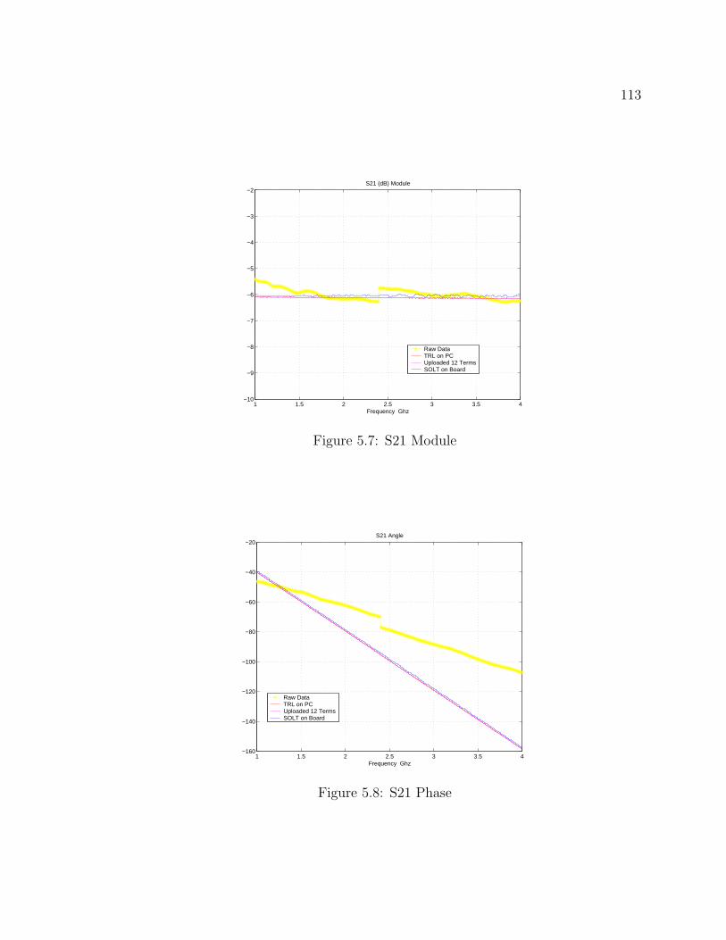
5.4 Coaxial Experimental Results
TRL Calibration and a DUT measurement with a Coaxial Kit were performed and
compared with another on board SOLT Calibration as an example of the automated
features that the software brings.
The selected DUT was a precision 6 dB SMA Coaxial Attenuator. A 30 mm length
Rigid Coaxial SMA connector was used as the LINE. As REFLECT the OPEN Loads
of a Mauryr Coaxial Calibration Kit were used.
With another feature of the program, the attenuation constant α of the LINE and
the ηeff = c/vph coefficient were calculated. Plots of the different magnitudes of Raw
data, Corrected DUT data and the actual Reflect coefficient Γa are provided.
From the plot of the DUT Reflection Coefficient S11 the DUT corrected data from
the TRL Calibration performed by the tool can be seen in a smooth trace. Around
this plot there is the trace (with ”ripple” wave form) of the DUT corrected data given
by the calibration performed with the uploaded 12 error terms calculated by the tool.
The other two calibration performed by the VNA firmware, the on board SOLT have
more irregular traces.
The graph highlights that the phase of DUT transmission coefficient S21 corrected
by the TRL Calibration performed has a linear behavior along the entire bandwidth
as opposed to the same coefficient S21 performed with a SOLT on board calibration
(performed with the same standards as the tool TRL calibration) that has phase skips
in the band.
112
1 1.5 2 2.5 3 3.5 4−80
−70
−60
−50
−40
−30
−20
−10
0S11 (dB) Module
Frequency Ghz
Raw DataTRL on PCUploaded 12 TermsSOLT on Board
Figure 5.5: S11 Module
1 1.5 2 2.5 3 3.5 4−200
−150
−100
−50
0
50
100
150
200S11 Angle
Frequency Ghz
Raw DataTRL on PCUploaded 12 TermsSOLT on Board
Figure 5.6: S11 Phase
113
1 1.5 2 2.5 3 3.5 4−10
−9
−8
−7
−6
−5
−4
−3
−2S21 (dB) Module
Frequency Ghz
Raw DataTRL on PCUploaded 12 TermsSOLT on Board
Figure 5.7: S21 Module
1 1.5 2 2.5 3 3.5 4−160
−140
−120
−100
−80
−60
−40
−20S21 Angle
Frequency Ghz
Raw DataTRL on PCUploaded 12 TermsSOLT on Board
Figure 5.8: S21 Phase
114
The LINE parameters like the attenuation constant α and the refractive index
for the phase velocity ηeff = c/vph are calculated from the measured propagation
constant γ and from the length difference ∆` = `line− `thru. The algorithm calculates
the eigenvalue matrix Λ of matrix (5.3.4) RM = TmL.(TmT )−1, rewritten in the same
way as equation (4.4.9) by doing:
RM = TmL.(TmT )−1 = T.Λ.T−1 =
[e−γ.∆` 0
0 e+γ.∆`
]=
[λ1 0
0 λ2
]= Λ (5.4.1)
By equating the eigenvalues and length difference ∆` properly, we take the mean
value of the attenuation constant α and the refractive index ηeff parameters, that are
calculated by the tool as follows:
〈α〉 = 1/2 · ln |λ1|+ ln |λ2|∆`
(5.4.2)
with
〈ηeff〉 =1
2πf∆`
∣∣∣ arctan[(=(λ1)/<(λ1)
]∣∣∣ +∣∣∣ arctan
[(=(λ2)/<(λ2)
]∣∣∣
(5.4.3)
and
εr = η2eff (5.4.4)
From the above measurement results, the calculated LINE parameters α and ηeff
are shown in Fig. 5.9 and Fig. 5.10:
115
1 1.5 2 2.5 3 3.5 40.002
0.004
0.006
0.008
0.01
0.012
0.014
0.016
0.018
0.02TRL Measurements α (dB/cm) vs Freq
α (d
B/c
m)
Frequency Ghz
Figure 5.9: LINE Attenuation constant
1 1.5 2 2.5 3 3.5 41.001
1.0015
1.002
1.0025
1.003
1.0035
1.004
1.0045
1.005
1.0055
1.006
TRL Measurements ηeff
vs Freq
η eff
Frequency Ghz
Figure 5.10: LINE ηeff coefficient
Chapter 6
Networks characterization andparameter extraction
6.1 Introduction
In this chapter the approaches used to characterize experimentally single two con-
ductors transmission lines and MTLs through the measurement of the Scattering
parameters will be given.
First the relevant methodologies used to extract the different transmission line
parameters R, L, G and C from direct measurements will be discussed. Then an ac-
curate extraction method from Scattering parameters matrix that takes into account
frequency dependency of R(f), L(f), G(f) and C(f) will be presented. An exam-
ple of measurement and extraction will be discussed and compared with theoretical
predictions of a full wave simulation.
Finally different methodologies for the extraction of the multi transmission line
parameter matrices R, L, C and G from Scattering matrix will be presented and the
results of an example will be discussed. Drawbacks and limitations will be highlighted
and discussed.
116
117
The parameter extraction methodologies included in this chapter are directly con-
nected with the useful implementation of different measurements of scattering pa-
rameters with the Measurement & Calibration Tool presented in last chapter.
It is remarked that a useful close set of measurements can be taken by a powerful
tool, and transmission line parameters can be fully and accurately characterized by
the measurements of the Scattering matrix with a single VNA instrument.
118
6.2 Transmission line characterization methods
Different methodologies are used to characterize a transmission line by direct mea-
surements. The more common experimental procedures [40] [26] [32] [33] and their
limitations will be presented. Then, a more accurate methodology [9] [10] that sur-
passes the classical methods’ limitations will be explained and an implementation
through a measurement of Scattering parameters will be discussed.
For any transmission line mode, the per-unit-length circuit parameters R, L, Gand C are defined in terms of the characteristic impedance Zc and the propagation
constant γ by:
γ
Zc
= G + jωC (6.2.1)
γZc = R+ jωL (6.2.2)
Then, if the characteristic impedance Zc and the propagation constant γ are
known, the per-unit-length circuit parameters R, L, G and C are given by:
R = <γZcL = =γZc/ωG = <γ/ZcC = =γ/Zc/ω
(6.2.3)
The problem consists in determining the propagation constant γ and the char-
acteristic impedance Zc through experimental methodologies, and then to solve the
equation system (6.2.3).
The measurement of the propagation constant γ is an easy task using the TRL
calibration, a subproduct of this procedure. Accurate results are given by this method
119
and it is used as the standard for its determination. Instead, one of the more prob-
lematic parameters to be measured is the characteristic impedance Zc and it only can
be estimated.
An approach based on the TRL calibration methodology that permits to estimate
the characteristic impedance Zc was given by J. Kasten et al [26]. This procedure
argues that Zc can be determined from a measurement of the propagation constant
γ and knowledge of the ”free-space capacitance”. The idea is attractive since γ is
readily determined using the TRL calibration.
The method supposes lossless conductors (R¿ ωL), then:
Zc ≈√LC =
1
vphC =1
cC0`(6.2.4)
where vph is the phase velocity, c is the free-space light velocity, C0 is the free-space
per-unit-length capacitance and ` is the transmission line structure length.
The drawback of this methodoloy is that it fails in low frequencies, therefore the
estimation of Zc by this method can be problematic.
Another procedure proposed by Marks and Williams [32] explores the possibility
of an alternative indirect prediction of Zc trough the measurement of γ by TRL
calibration. The method, while approximate, was demonstrated quite precise for
quasi-TEM lines with low substrate losses [31].
This analysis supposes that when the substrate loss is low and the transverse
currents in the conductors are weak, as is typically true at very high frequencies,
then G is negligible (G ¿ ωC). With this approximation the (6.2.1) becomes:
120
γ
Zc
= G + jωC ≈ jωC (6.2.5)
and
Zc ≈ γ
jωC (6.2.6)
In order to predict the value of the characteristic impedance Zc, this method
proposes an experimental measurement of the propagation constant γ and the pul
capacitance C.
There are different methodologies to measure the pul capacitance C and their
goal is the accuracy and complexity of the measurement. Approximate procedures
were presented in [33] with a reasonable complexity. The first one is based on the
measurement of the per-unit-length dc resistance Rdc, an easily measurable quantity.
The procedure takes the imaginary part of the product of (6.2.1) and (6.2.2):
RC + LG = <(
γ2
jω
)(6.2.7)
In the case of low losses substrates G is small at microwaves frequencies and
LG ¿ RC. If R is approximately equal to the per-unit-length DC resistance Rdc,
then equation (6.2.7) becomes:
C ≈ 1
Rdc
<(
γ2
jω
)(6.2.8)
121
These approximate values are expected to deviate significantly from the actual
value except at low frequencies, where the current in the conductors is highly uniform
and the approximation R ≈ Rdc is valid. For this reason, a least squares fit of a
quadratic to the approximation of C is used to extrapolate to DC.
To achieve realistic results in low frequencies, another measurement is proposed
in the same work [33] where a small lumped resistor is measured at low frequencies
giving:
Zc1 + Γload
1− Γload
= Zload ≈ Rload,dc (6.2.9)
where Rload,dc is the dc resistance of the lumped load and Γload is its complex
measured reflection coefficient. Substituting (6.2.9) in (6.2.1) gives:
C[1− j(G/ωC)] ≈ γ
jωRload,dc
1 + Γload
1− Γload
(6.2.10)
In Ref. [33], a least-squares to fit a quadratic to the measured values of C was
used to extrapolate the approximate values of C to dc. Approximate values of G/ω
are also obtained with this technique. Limitations of this technique are that it is
only applicable to quasi-TEM lines but not necessarily to other types of waveguides
mainly in the case of lossy substrates where the approximation G ¿ ωC is not valid.
Added to this, the approximations and complexity of measurements allow for further
errors.
A different approach, based on a single measurement of the Scattering parameters
is shown and used in the following paragraphs of this work. This technique does not
122
assume approximations and uses the full information given by the S-matrix.
123
6.2.1 Circuit parameters extraction from S-Matrix
The above traditional approaches used to extract the per-unit-length circuit parame-
ters R, L, G and C assume resistance and capacitance constant with frequency. These
assumptions are inaccurate when high frequency transmission parameters need to be
extracted because they strongly depend on the frequency.
A different methodology based on the direct extraction of the Telegrapher’s equa-
tion per-unit-length circuit parameters R, L, G and C from S-parameter measurements
was proposed by W. Eisenstadt [9] [10].
This procedure characterizes interconnections and transmission lines using stan-
dard on-chip microwave probing directly from S-parameter measurements. Standard
automated microwave test equipment can be used to obtain results.
The theoretical basis of the method is Telegrapher’s equation taking into account
the frequency dependency of the per-unit-length circuit parameters R(f), L(f), G(f)
and C(f).
The S-parameter responses measured from a lossy unmatched transmission line
with length `, propagation constant γ, characteristic impedance Zc and a controlled
reference impedance Zref are [27]:
[S] =1
DS
[(Z2
c − Z2ref ) sinh(γ`) 2ZcZref
2ZcZref (Z2c − Z2
ref ) sinh(γ`)
](6.2.11)
where
DS = 2ZcZref cosh(γ`) + (Z2c + Z2
ref ) sinh(γ`)
The above matrix is assumed symmetrical and contains two independent linear
equations. This S-parameter matrix is converted to ABCD parameter matrix as:
124
[ABCD] =
[cosh(γ`) Zc sinh(γ`)
Zc sinh(γ`) cosh(γ`)
](6.2.12)
and the relationship between the S-parameters and the ABCD matrix is [7]:
A = (1 + S11 − S22 −∆S)/(2S21)
B = (1 + S11 + S22 + ∆S)Zref/(2S21)
C = (1− S11 − S22 + ∆S)/(2S21Zref )
D = (1− S11 + S22 −∆S)/(2S21)
(6.2.13)
where
∆S = S11S22 − S21S12
Combining equations (6.2.11) to (6.2.13) yields [9]:
e−γ` =
1− S2
11 + S221
(2S21)2±K
−1
(6.2.14)
where
K =
(S2
11 − S221 + 1)2 − (2S11)
2
(2S21)2
1/2
(6.2.15)
and
Z2c = Z2
ref
(1 + S11)2 − S2
21
(1− S11)2 − S221
(6.2.16)
125
Once γ(f) and Zc(f) are determined from (6.2.12)and (6.2.14), Telegrapher’s equa-
tions model per-unit-length circuit parameters R(f), L(f), G(f) and C(f) are given
The procedure converges very well for small length ` segments of transmission
line, being the convergency bandwidths limited by this length `. It is shown that the
procedure is independent of the calibration technique used to extract the calibrated
Scattering matrix parameters.
This procedure was used in our work to extract the per-unit-length circuit param-
eters from the S-parameters matrix measured with a VNA HP8510C of a two port
CPW structure and the results where compared with a Full Wave EM simulation to
validate the experimental performance of the method.
Results of the parameter extraction and calibrated Scattering matrix are given,
and compared with the simulated CPW structure data.
126
6.2.2 On Wafer measurements and characterization
Modern VNAs can easily make accurate measurements in situations where calibration
standards can be connected to the test ports. There are, however, many devices that
cannot be connected directly to the test port of a VNA and require a fixture system or
on-wafer probe to complete the bridge between the DUT and the test instrumentation.
The use of test fixtures presents problems and additional errors are introduced in the
measurement process.
Mainly network analysis, in the general situation, is used to characterize the linear
behavior of a device. The data resulting from the measurements will not be truly
accurate because of imperfections in the instrument and in the hardware used to
connect the device. As was seen in previous chapters, random errors, including drift,
noise and repeatability are difficult to handle but systematic errors can be addressed
by means of calibration techniques.
Some of the problems specific to the fixtured measurements include connection
repeatability and difficulty in providing reference standards. In addition, the nature
of the transmission medium may include dispersion, losses and other problems which
make it difficult to establish a reliable, known characteristic impedance.
A number of factors need to be considered to measure with a microwave test fixture
[42]:
• Compatibility: Many devices have performances which are strongly depen-
dent on the environment in which they are embedded and it is therefore neces-
sary to provide an environment similar to that used in the application. This is
met by arranging for a similar physical geometry in the measurement environ-
ment, ensuring that the field configuration in the vicinity of the device closely
127
matches that of the application and is more likely to give useful data. The
fixture is optimized for the range of impedances being measured and this may
require that the fixture transforms the measurement environment impedance.
• Calibration: The success for fixture design is the calibration technique to be
used. The very nature of a test fixture is such that conventional calibration
techniques are unsuitable because the device to be tested does not have ports
terminated in precision connectors. There are two distinct approaches for de-
embedding device measurements from those of a fixture.
The first method consists in calibrating the VNA system at reference planes of
the device by employing calibration components which replace the DUT within
the fixture. The method is very simple in principle and relies only on the quality
of the calibration components, the repeatability of the fixture and the validity
of the calibration algorithms. In this case all the discontinuities, losses, etc. are
all included in the Error models of the fixture.
The second method uses a model for the fixture and with de-embeds the device.
Such a model may be as simple as a length of transmission line at the test port
or include complications due to multiple discontinuities, losses, etc. There are
many combined possibilities involving calibration at accessible reference planes
which are as close as possible to the device in conjunction with a model with
the minimum complexity. The majority of these imperfections are not included
in the Error models and need to be added to the total fixture to implement the
de-embedding process.
In our measurement the first method was used, then all the imperfections between
128
probe tips and contacts with the transmission line measured where included in the
Error Boxes of the fixture’s Error model.
Measurements were made with reference planes coinciding with the position of the
probe tips in contact with the DUT. Then, differences between measurement values
and simulation values can be attributed to the extraction process methodology used
and/or the accuracy of the simulated model, but no to the imperfections of the fixture.
The extraction methodology [9] presented in the last section, was validated by a
measurement of a Coplanar Waveguide CPW with stratified dielectric that was made
by implementing the calibration techniques and measurement tools presented in the
last chapters. Results were compared with a Full Wave EM simulation [14][15] of the
CPW structure. In Fig. 6.1 the front view of the tested CPW structure1 is shown. A
sample of this CPW structure of a length of 2.585 mm was simulated and measured
within a bandwidth from 1 to 6 Ghz.
As can be seen from Figs. 6.2 and 6.3, the extracted per-unit-length circuit pa-
rameters L(f) and C(f) are in good agreement with the FW simulation model’s
parameters. A disagreement is shown in Figs. 6.4 and 6.5 for the per-unit-length
circuit parameters R(f) and G(f). For the parameter R(f), the simulated model
predicts a lower influence of the skin effect on the structure behavior. The difference
can be explained by the assumption that in the measurement the microwave measure-
ment fixture probe tips were not deembedded, giving an additional contribution for
dispersion losses. The simulated dielectric losses, present in G(f), are greater than
the measured data. Causes for this behavior can be attributed to the assumption of
a highly lossy dielectric synthesized Debye model [1] for the complex permittivity ε.
1CPW structure data were provided by Prof. Franco Fiori of the EMI Microwave Group atPolitecnico di Torino, Italy
129
Figure 6.1: CPW stratified dielectric structure
An excellent match is achieved between the simulated and measured characteristic
impedance Zc as shown in Figs. 6.6 and 6.7, when the differences are attributed to
the microwave measurement fixturing, where the de-embedding process did not include
the probe tips interfaces.
The measured and simulated attenuation constant α shown in Fig. 6.8 are in
excellent agreement, where differences at high frequency becomes evident due to the
over valuated dielectric losses in the simulated model. The measured refractive index
ηeff presents a close behavior to the FW simulated model as is seen in Fig. 6.9.
130
1 2 3 4 5 60
2
4
6
8
10
Frequency, GHz
L, n
Hy/
cmMeasurementFW Simulation
Figure 6.2: per-unit-length Inductance nHy/cm
1 2 3 4 5 62
4
6
8
10
12
14
16
Frequency, GHz
C, p
F/c
m
MeasurementFW Simulation
Figure 6.3: per-unit-length Capacitance pF/cm
131
1 2 3 4 5 60
10
20
30
40
50
Frequency, GHz
R, Ω
/cm
MeasurementFW Simulation
Figure 6.4: per-unit-length Resistance Ω/cm
1 2 3 4 5 60
0.05
0.1
0.15
0.2
Frequency, GHz
G, S
/cm
MeasurementFW Simulation
Figure 6.5: per-unit-length Conductance S/cm
132
1 2 3 4 5 60
10
20
30
40
50
Frequency, GHz
Zc
Mod
ule,
ΩMeasurementFW Simulation
Figure 6.6: Module of the Characteristic Impedance Zc
1 2 3 4 5 6−60
−40
−20
0
20
40
60
Frequency, GHz
Zc
Ang
le, Ω
MeasurementFW Simulation
Figure 6.7: Phase of the Characteristic Impedance Zc
133
1 2 3 4 5 60
5
10
15
20
25
Frequency, GHz
α, d
B/c
mMeasurementFW Simulation
Figure 6.8: Attenuation dB/cm
1 2 3 4 5 61
2
3
4
5
6
7
8
9
10
Frequency, GHz
nef
f
MeasurementFW Simulation
Figure 6.9: Refraction index ηeff
134
6.3 MTL characterization methods
Various parameter extraction techniques for MTL structures were studied and valu-
ated. A brief discussion follows and finally an example in which an accurate technique
without optimization [38] is implemented will be presented.
Groudis and Chang [23] have previously developed a frequency domain method
to extract parameter matrices R, L, C and G from the two-port impedance Z and
admittance Y matrices. This method is based on a combination of the method of
characteristics and the decoupled mode transformation in frequency domain. In this
procedure, the solution of the MTL equations (2.3.12) and (2.3.13) is assumed as
follows:
V = A.exp(−Γz) + B · exp(Γz) (6.3.1)
Y−1C I = A.exp(−Γz)−B.exp(Γz) (6.3.2)
where
Γ = (ZY)1/2 = PγP−1 (6.3.3)
YC = Z−1Γ = YΓ−1 (6.3.4)
P is the eigenvector matrix of Γ. It is also the eigenvector matrix of the ZY prod-
uct, being γ the diagonal eigenvalue matrix of Γ. Applying properties the following
relationship is derived:
exp(−Γz) = Pexp(−γz)P−1 (6.3.5)
135
In the solution it is assumed that the matrix Γ = (ZY)−1 exists and that the
characteristic admittance matrix YC is symmetrical. Following the reasonings given
in [41], a MTL with n+1 conductors of length d can be treated as a 2n-port network,
having n ports on the input end (subindex i) and n ports on the output end (subindex
o). Then, it can be proven [7] that:
[Ii
Io
]=
[YC cothΓd −YC sinh−1 Γd
−YC sinh−1 Γd YC cothΓd
]·[
Vi
Vo
](6.3.6)
with a short-circuit admittance matrix Y2n of the 2n-port network given as:
Y2n =
[YA YB
YB YA
](6.3.7)
where
YA = YC cothΓd
YB = −YC sinh−1 Γd(6.3.8)
and
cothΓd = P(coth γd)P−1
sinh−1 Γd = P(sinh−1 γd)P−1(6.3.9)
And, the open-circuit impedance matrix Z2n is given by:
Z2n =
[ZA ZB
ZB ZA
](6.3.10)
where
ZA = (cothΓd)Y−1C
ZB = (sinh−1 Γd)Y−1C
(6.3.11)
136
Two methods to derive the YC and Γ matrices were proposed in [23]. The first one
is to be used when the transmission line attenuation is small, and it is not interesting
for lossy lines.
The second method is to be used with high attenuation or lossy lines. This case
may occur either because the line is sufficiently long, or because the frequency of
interest is so high that losses due to skin effect and proximity effect are significant.
It involves measurements at both input and output ends of the MTLs.
A brief discussion of this method is provided in the following. From equation
(6.3.7) we have:
−Y−1B YA = coshΓd (6.3.12)
Γd = P(cosh−1 Λ)P−1 (6.3.13)
where P is the eigenvector matrix of Γd and −Y−1B YA. Equations (6.3.3) and
(6.3.13) give:
γd = cosh−1 Λ (6.3.14)
and from (6.3.7) and (6.3.13) the characteristic admittance matrix YC is found
to be:
YC = −YB sinhΓd
= −YBP[sinh(cosh−1 Λ)]P−1(6.3.15)
This, from (6.3.14) the per-unit-length modal attenuation constant αm and per-
unit-length modal phase constant βm are obtained by dividing the real and the imag-
inary parts by d and ωd respectively.
137
Then, the per-unit-length parameters R, L, C and G can be derived by replacing
and equating into (6.3.4) the results Γ and YC respectively obtained from (6.3.13)
and (6.3.16), as follows:
Z = R + jωL = ΓY−1C
Y = G + jωC = YCΓ(6.3.16)
This method was tested by using a Full Wave EM simulation2 on a 4-Ports asym-
metric microstrip line and it was found not to achieve symmetry for the above per-
unit-length parameters R, L, C and G and to produce results without physical
meaning. Reasons for this are that the procedure presupposes symmetries for Z and
Y up to frequencies under the Ghz region, in which their authors have validated it.
As was explained in last chapters, these symmetries are intended to be broken in high
lossy media, as in high frequency, this the procedure needs to be modified to take
asymmetries into account.
A great limitation of the method is that it needs to be optimized by a proper
algorithm. Another drawback is that the convergency bandwidth is limited by the
heuristic rule of thumb `MTL ≤ λ/10, where `MTL is the MTL length in the prop-
agation direction and λ is the wavelength of the EM wave propagating along the
structure.
Another methodology was developed by Knockaert et al [29] to recover lossy MTL
parameters from Scattering matrix. The method is based on a generalization of the
simultaneous diagonalization technique by means of congruence transformations to
the general lossy reciprocal case.
2Simulation was made with the EM simulator EMSight of AWR, that includes a fast Full Waveelectromagnetic solver based in a modified Spectral-domain method of moments.
138
This procedure is based on the symmetry and reciprocity properties of the Z and
Y matrices, and the solution is obtained through the chain parameter matrix Φ(z)
defined in equations (2.3.16) and (2.3.17), that is rewritten as:
Φ(z) = exp
− z
(0 Z
Y 0
)=
[Ω α
β ΩT
]
=
[φ1
(z2ZY
) −zZφ2
(z2ZY
)
−zYφ2
(z2ZY
)φ1
(z2ZY
)] (6.3.17)
where the superscript T indicates Hermitian adjoint matrix (conjugate transpose)
and the entire functions φ1(z) and φ2(z) are defined as:
φ1(z) = cosh(√
z)
φ2(z) = sinh(√
z)/√
z(6.3.18)
Noting that α and β are symmetric, also Ωα and βΩ are symmetric. The authors
of [29] assume that Ω2 = In + αβ (with In is the n× n identity matrix) and that the
following relation needs to be achieved:
[Ω α
β ΩT
]·[
Ω −α
−β ΩT
]=
[In 0
0 In
]= I2n (6.3.19)
With this assumptions, the 2n× 2n Z2n-matrix description of a MTL is given by:
[Vi
Vo
]=
[Z2n
] ·[
Ii
Io
](6.3.20)
139
and based on the symmetry assumption:
Z2n =
[A B
B A
]=
[−β−1ΩT −β−1
α− Ωβ−1ΩT −β−1Ω−1
](6.3.21)
where A and B are symmetric n× n matrices. These relationships follow:
β = −B−1, Ω = AB−1, α = B − AB−1A (6.3.22)
With the matrices A and B given from the Z2n-matrix description, the Z and Y
matrices are recovered from the equations:
AB−1 = φ1
(z2ZY
)
B−1 = −zYφ2
(z2ZY
) (6.3.23)
By assuming that the eigenvalues of AB−1 and ZY are all distinct, the resulting
decompositions are given as:
AB−1 = PδzP−1, ZY = PδtP
−1 (6.3.24)
and the related simultaneous congruence decompositions given by
A = PδaPT , B = PδbP
T , Z = PδrPT , Y = P−T δgP
−1 (6.3.25)
Using the above relationships, the following equations for the δ(·) diagonal matrices
were derived [29]:
δaδ−1b = δz
δrδg = δt
δz = φ1(z2δt)
δ−1b = zδgφ2(z
2δt)
(6.3.26)
140
From the above equations, the MTL parameters can be obtained from the Z2n-
matrix. The following general formula is derived:
δt =1
z2[arg cosh(δz) + j2πδn]2 (6.3.27)
where δn is a diagonal matrix with integer entries that takes into account the
multiple branches of the inverse function of φ1(z) = cosh(√
z).
This algorithm intends to solve (6.3.27) specifying an index vector of integers, the
entries of the diagonal matrix δn, in order to retrieve the correct MTL parameters. It
has a direct connection with the MTL length z, since the method tries to find T from
a matrix exponential exp(zT). For the scalar case this creates phase related problems
to be solved to obtain an estimate for λ, given t = eλz. Approximations for this scalar
case are generalized to the matrix exponential and a general solution, that includes
the generation of the index vectors, was developed in [29].
The author of the present work has tested the mentioned algorithm in a 4-Ports
asymmetric microstrip line simulated with a Full Wave EM simulation3. Limitations
due to convergency problems were encountered in solving (6.3.27), where a difficulty
to reach diagonal matrices needs to be optimized in the original algorithm. In this
procedure, symmetries for Z and Y matrices were assumed, thus high lossy MTL
structures are not properly characterized.
Other approaches are proposed in the literature [25][38][48][49]. The procedure
presented by Arz et al [48] uses statistical measurement methodology based on Marks
algorithm [35] as an enhancement of the TRL algorithm.
3Simulation was made with the EM Full Wave simulator EMSight of AWR.
141
In the present work a procedure that doesn’t require optimization [37][38] and
that gives accurate results was implemented. A discussion of the method, examples
of characterization and limitations are given in the following paragraphs.
142
6.3.1 MTL parameters extraction from S-Matrix
A method for extracting the circuit models for MTLs from black-box parameters
was developed by Martens and Sercu [38]. If the number of conductors in a MTL is
large, the model will have many parameters to be extracted and non physical values
may be obtained or the extraction process does not converge as was seen in previous
paragraphs. Simultaneous optimization requires great computational effort and needs
error estimation routines.
The direct extraction method without optimization is valid for small MTL lengths
compared with wavelengths of propagating waves. If T or Π circuit models are pro-
posed, a direct relation is found between the Z and Y matrices and the circuit
parameters.
A brief explanation is given: an MTL with 2n access ports is considered, then if
two RL sections and one GC section (T-circuit model) or two GC sections and one RL
section (Π-circuit model) are sufficient to obtain an accurate model, no optimization
process is needed to determine the parameter values of the model [38]. They can be
directly calculated from the black-box Scattering parameters.
We consider a (n+1) conductors MTL, the 2n×2n S-matrix consists in four n×n
submatrices as follows [25]:
S =
[Sin,in Sin,out
Sout,in Sout,out
](6.3.28)
Then, we can find the impedance Z2n and admittance Y2n matrices from the
143
Scattering matrix as:
Z2n = Zref · [I+ S][I− S]−1
Y2n = Z−1ref · [I− S][I+ S]
(6.3.29)
where I is the 2n×2n identity matrix. To obtain the parameter values the 2n×2n
Z2n and Y2n are defined as:
Z2n =
[Zin,in Zin,out
Zout,in Zout,out
]and Y2n =
[Yin,in Yin,out
Yout,in Yout,out
](6.3.30)
Then the per-unit-length parameters R, L, C and G of the T-circuit model, as
shown in Fig. 6.10, are related to the above matrices as follows:
R(1) = <(Zin,in − Zin,out)
L(1) = =(Zin,in − Zin,out)/ω
C = =(Z−1in,out)/ω
G = <(Zin,out)
R(2) = <(Zout,out − Zin,out)
L(2) = =(Zout,out − Zin,out)/ω
for T circuit (6.3.31)
where the supraindex (1) indicates the input RL branch of the T-circuit model and
the supraindex (2) indicates the output T-circuit model RL branch.
144
Figure 6.10: MTL T-circuit model
In an analogue way, the per-unit-length parameters R, L, C and G of the Π-circuit
model, as shown in Fig. 6.11, can be found from the following relationships:
G(1) = <(Yin,in + Yout,in)
C(1) = =(Yin,in + Yout,in)/ω
R = <(−Y−1out,in)
L = =(−Y−1out,in)/ω
G(2) = <(Yout,out + Yout,in)
C(2) = =(Yout,out + Yout,in)/ω
for Π circuit (6.3.32)
where the supraindex (1) indicates the input GC branch of the Π-circuit model
and the supraindex (2) indicates the output Π-circuit model GC branch.
Although this methodology was originally developed for small high-speed IC inter-
connections, it was proven to work very well for MTLs with lengths `MTL ≤ λmin/20
being λmin the wavelength for the maximum frequency propagated along the line.
145
Figure 6.11: MTL Π-circuit model
The major advantage of the direct calculation method is that a very accurate
model is obtained quickly. A disadvantage is that the model is only valid for lengths
that are small with respect to the wavelength.
In the next paragraphs the experimental results of a simulation and characteri-
zation of a 4-Ports asymmetric coupled microstrip line structure using the present
methodology will be discussed.
146
6.3.2 MTL simulation and experimental results
A 4-Port asymmetric coupled microstrip line structure was tested through the method
discussed in the last section. It was assumed that the signal paths are connected
from the ground plane to the signal conductors, and coupled modes are intended to
be propagated through the line.
A geometry of the structure with length `MTL = 1 mm is shown in Fig. 6.12
where the 30 µm wide signal conductor on the left is separated from the 200 µm wide
signal conductor on the right by a 50 µm wide gap. The 100 µm thick substrate has
a relative dielectric constant of 12.9. The 0.5 µm thick signal conductors and 5 µm
thick ground plane have a conductivity σ = 3.602× 10⁷ S/m.
Figure 6.12: Asymmetric Coupled Microstrip Line
A Full Wave EM simulation of the structure’s behavior was performed by using the