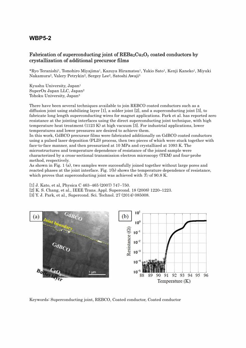
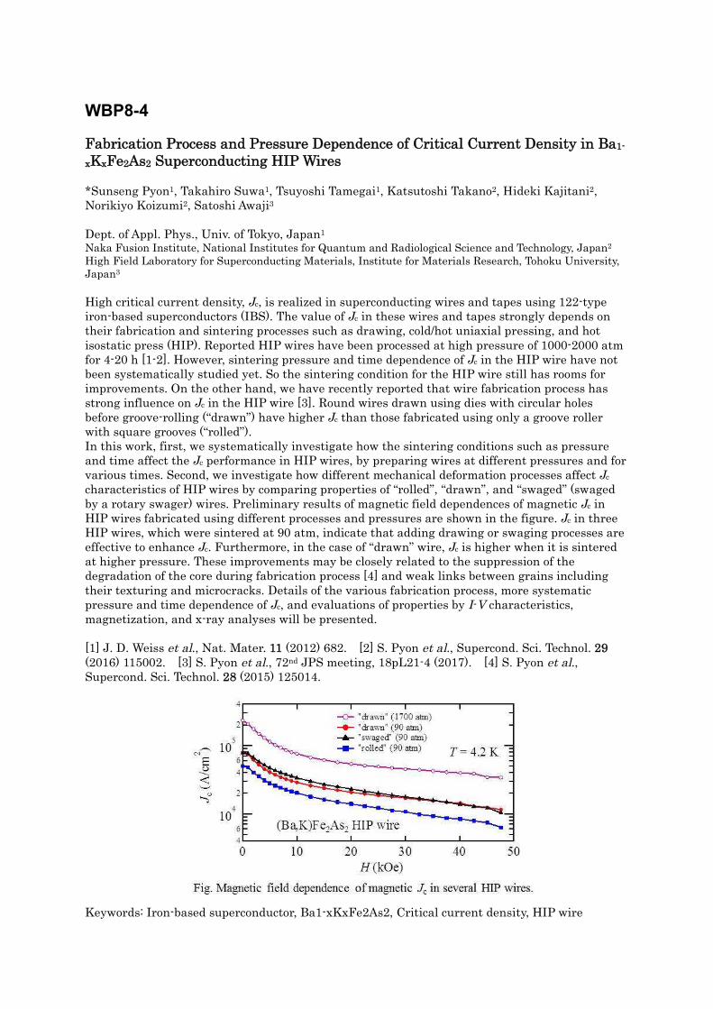
WB1-1-INV Development of BMO-doped REBCO Coated Conductor by Hot-Wall PLD Process on IBAD template *Yasuhiro Iijima 1 Fujikura Ltd. 1 During the past two decades, tremendous R&D efforts were concentrated on development of high- performance and high throughput processing for REBCO coated conductors. We had chosen combined process of vapour-phase production techniques by using large-area ion-beam-assisted- deposition (IBAD), and hot-wall type pulsed-laser-deposition (PLD), which realized quite homogeneous crystalline growth conditions for REBCO by furnace-like, nearly equilibrium substrate heating. As a results, reliable production line of non-doped REBCO tapes with lengths over 500 m was developed with typical Ic performances over 500 A/cm at 77 K in the self-field and over 1000 A/cm (Jc=5-6 MA/cm 2 ) at 30 K in 2 T[1]. Recently we applied the process for introduction of rod-like APC as BaMO3 (BMO, M : Zr or Hf) - doped REBCO conductors, though multiplied deposition parameters come from nano-rod BMO growth should cause narrower process windows. We found a productive process condition of BMO- doped high-performance tapes with good longitudinal homogeneity[2]. 300m long class uniform BaHfO doped EuBCO tapes were formed with productive high growth rate of 20-30 nm/sec, being faster than commercial non-doped conductors, which had also large Ic of 1700-1800A/cm (Jc=7-8 MA/cm 2 ) at 30K, 2T. 600-1000m long run is now on-going. The angular dependence of in-field Jc properties were investigated in wide temperature range, and strongly c-axis correlated flux pinning were observed over 30K, especially in those films with the growth rate limited lower than 5 nm/sec, where the minimum values of Jc were not so different from high growth rate over 20 nm/sec. These results indicate reliable controllability of deposition parameters on high-rate APC introduction by using hot-wall PLD process. This Paper includes the results supported by the New Energy and Industrial Technology Development Organization (NEDO). [1] Y. Iijima, et al., IEEE Tran.s. Appl. Supercond., vol. 25, no. 3 (2015) , Art. no. 6604104. [2] Y. Iijima, et al., IEEE Tran.s. Appl. Supercond., vol. 27, no. 4 (2017) , Art. no. 6602804. Keywords: Coated Conductor, REBCO, Artificial Pining Center, Pulsed Laser Deposition
Transcript
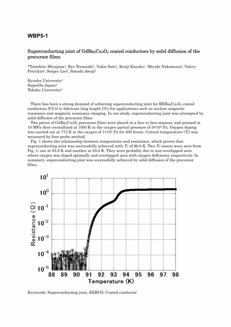
WB1-1-INV Development of BMO-doped REBCO Coated Conductor by Hot-Wall PLD Process on IBAD template *Yasuhiro Iijima1 Fujikura Ltd.1 During the past two decades, tremendous R&D efforts were concentrated on development of high-performance and high throughput processing for REBCO coated conductors. We had chosen combined process of vapour-phase production techniques by using large-area ion-beam-assisted-deposition (IBAD), and hot-wall type pulsed-laser-deposition (PLD), which realized quite homogeneous crystalline growth conditions for REBCO by furnace-like, nearly equilibrium substrate heating. As a results, reliable production line of non-doped REBCO tapes with lengths over 500 m was developed with typical Ic performances over 500 A/cm at 77 K in the self-field and over 1000 A/cm (Jc=5-6 MA/cm2) at 30 K in 2 T[1]. Recently we applied the process for introduction of rod-like APC as BaMO3 (BMO, M : Zr or Hf) -doped REBCO conductors, though multiplied deposition parameters come from nano-rod BMO growth should cause narrower process windows. We found a productive process condition of BMO-doped high-performance tapes with good longitudinal homogeneity[2]. 300m long class uniform BaHfO doped EuBCO tapes were formed with productive high growth rate of 20-30 nm/sec, being faster than commercial non-doped conductors, which had also large Ic of 1700-1800A/cm (Jc=7-8 MA/cm2) at 30K, 2T. 600-1000m long run is now on-going. The angular dependence of in-field Jc properties were investigated in wide temperature range, and strongly c-axis correlated flux pinning were observed over 30K, especially in those films with the growth rate limited lower than 5 nm/sec, where the minimum values of Jc were not so different from high growth rate over 20 nm/sec. These results indicate reliable controllability of deposition parameters on high-rate APC introduction by using hot-wall PLD process. This Paper includes the results supported by the New Energy and Industrial Technology Development Organization (NEDO). [1] Y. Iijima, et al., IEEE Tran.s. Appl. Supercond., vol. 25, no. 3 (2015) , Art. no. 6604104. [2] Y. Iijima, et al., IEEE Tran.s. Appl. Supercond., vol. 27, no. 4 (2017) , Art. no. 6602804. Keywords: Coated Conductor, REBCO, Artificial Pining Center, Pulsed Laser Deposition
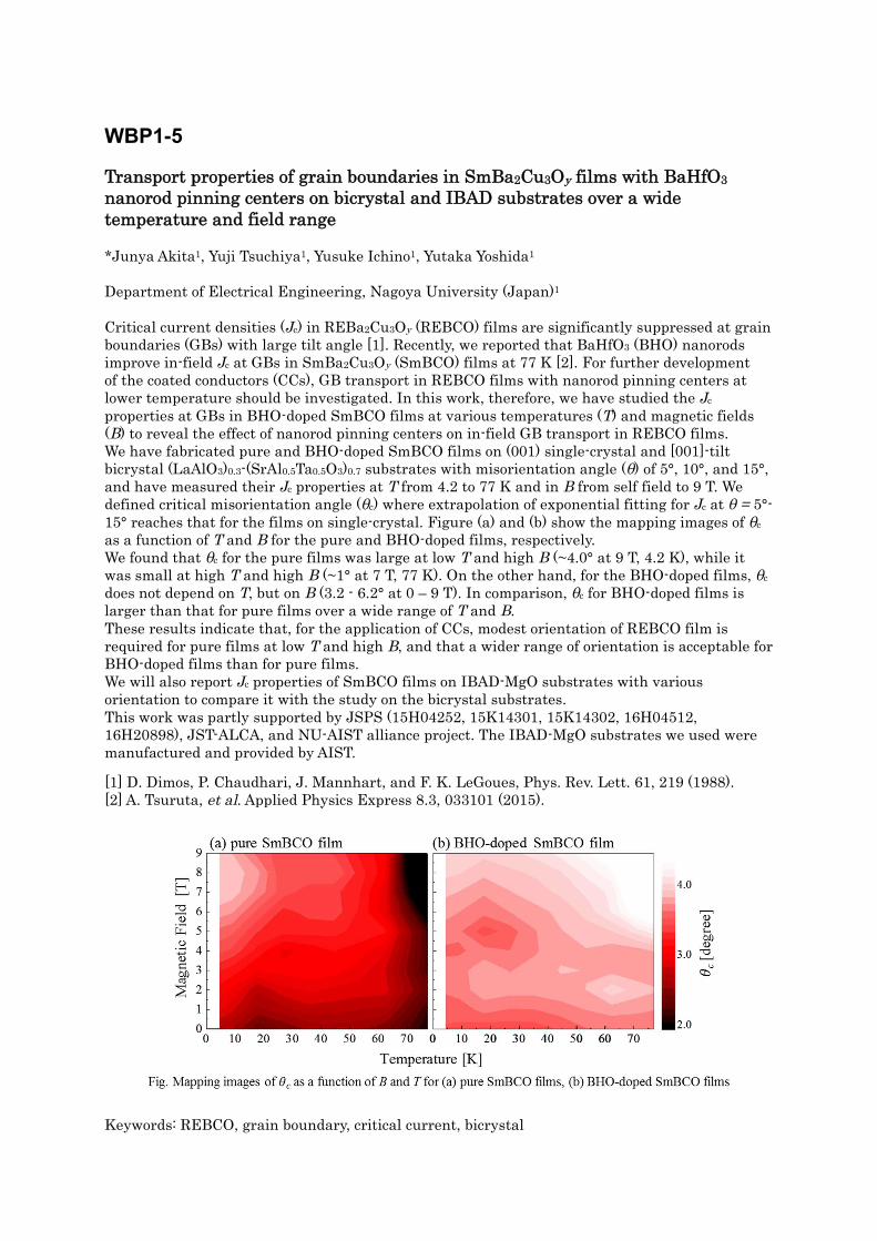
WB1-2-INV Recent progress on the development of RE-123 CCs in SuNAM *Seung Hyun Moon1 SuNAM Co. Ltd., Anseong-Si, Gyeonggi-do, Korea1 SuNAM has been producing long-length coated conductors based on a proprietary process which consists of electron beam co-evaporation of constituent metals and subsequent conversion of precursor film to superconducting phase by carefully controlling temperature and oxygen pressure. After securing stable manufacturing routine for upto 1 km-long wires, with about 10 percent uniformity in critical current enabled by various quality control measures, we tried to further increase critical current above 1,000 A/cm-width. This goal should be achieved by increasing thickness of superconducting layer while retaining critical current density, or even enhancing it. We varied co-evaporation process to enhance composition uniformity, and also modify temperature and pressure profile in heat treatment furnace to better utilize conversion dynamics of GdBa2Cu3O7-x phase formation, and the results will be presented. With these wire, we made 400 mH compact reactor with cryogen free operation. The reactor’s operating current is over 1,500 A at temperature is around 10 K. Detailed design, construction, and operating results will be discussed. And first all HTS CC base commercial 18 T magnet result will be introduced. A 70 mm cold bore high temperature superconducting (HTS) magnet was developed for axion detector system of Center for Axion and Precision Physics (CAPP) research center in Institute for Basic Science (IBS) in the Republic of Korea. A key parameter for axion detector magnet is to generate high and longitudinally uniform magnetic field in RF cavity. Magnetic field strength on -100 mm < z < 100 mm in coil bore space should be larger than 90 % of it at magnet center. Finally we’ll summarize a commercialization & industrialization efforts in Korea, and suggest a key issues to open the true market. This work was supported by the Power Generation & Electricity Delivery Core Technology Program of the Korea Institute of Energy Technology Evaluation and Planning(KETEP) granted financial resource from the Ministry of Trade, Industry & Energy, Republic of Korea (No. 20131010501800).
WB1-3-INV Development and production of advanced 2G HTS wires at SuperOx *Sergey Samoilenkov1, Alexander Molodyk2, Sergey Lee3, Valery Petrykin3 SuperOx, Nauchnyi proezd, 20, bld.2, Moscow, Russia1 S-Innovations, Presnenskaya embankment, 8, bld.1, Moscow, Russia2 SuperOx Japan, SIC-3, 1880-2 Kamimizo, Chuo-ku Sagamihara, Kanagawa 252-0243, Japan3 Applications of high temperature superconductors (HTS) demand a supply of significant amounts of a superconducting wire. The group of SuperOx companies develops a technology route to the future high-volume market of these superconducting materials. We employ highly reproducible and scalable industrial vacuum technologies such as IBAD and PLD to fabricate 2G HTS wire with a superior quality. The advanced chemical processes help us to customize a superconducting wire, making it optimal for particular requirements of each application type. In this talk, the overview of the recent progress will be provided, including the increase of production capacity with the installation of a new production line, description of techniques used in SuperOx for in situ and ex situ quality control, as well as the results of the introduction of artificial pinning centers in SuperOx wire. Some examples of final products made from SuperOx 2G HTS wire will be shown demonstrating the viability of the company’s approach to the advanced 2G HTS wire technology. Finally, the outlook will be given with the directions of a future work to make high quality 2G HTS wires readily available. Keywords: 2G HTS wire, in situ quality control, customization, production
WB1-4-INV Production and Development of ReBCO (2G-HTS) Conductors *Toru Fukushima1, Drew W. Hazelton1, Yifei Zhang1, Aarthi Sundaram1, Satoshi Yamano1, Hiroshi Kuraseko1, Hisaki Sakamoto2, Kengo Nakao2, Ryusuke Nakasaki2, Masayasu Kasahara2 SuperPower Inc.1 Furukawa Electric Co., Ltd.2 The potential applications of Rare-Earth Barium Cupper Oxide (ReBCO), Second-Generation High-Temperature Superconductors (2G-HTS), have been demonstrated in many projects for the last several years. This would indicate the ReBCO conductor is now being considered a robust and feasible solution to advanced devices and systems toward the future. This paper describes recent approaches to improve the design and performance of ReBCO conductors. One of the key challenges is to best-align the design of films in terms of different operating conditions, by taking trade-off of many aspects into account; not only for the performances, but also for the manufacturability and reliability. The other approach is to provide compact and robust profiles to suit the various needs in assembly of high-field coils, or cable-conduit for larger scale devices. Authors will address to those issues and present the recent progress for ReBCO conductors. Keywords: High Temperature Superconductors, ReBCO
WB2-1 Structural, mechanical and electrical characterization of long length REBCO tapes for FCL applications *Sandra Kauffmann-Weiss1, Mayraluna Lao1, Simon Otten1, Veit Große2, Markus Bauer2, Bernhard Holzapfel1, Jens Hänisch1 Institute for Technical Physics, Karlsruhe Institute of Technology, Karlsruhe, Germany1 THEVA Dünnschichttechnik GmbH, Ismaning, Germany2 One promising solution for renewable electricity over long distances is the realization of high voltage DC super-grids, but the management of fault currents remains an issue even if DC circuit breakers have emerged. Superconducting Fault Current Limiters (SCFCLs) using REBCO tapes have proved their outstanding performances for fault current limitation on medium voltage AC systems and it is already demonstrated that these tapes can be produced in the necessary length for FCL applications. However, to realize advanced cost-effective REBCO tapes, first the characteristics of the tapes have to be improved further. The aim of European project FASTGRID (Cost effective FCL using advanced superconducting tapes for future HVDC grids) is the property improvement of the REBCO tapes in order to significantly enhance the electric field limit that leads to economical attractiveness of SCFCL for high voltage DC applications. High critical currents will help to reduce the cost as the absolute length of the tapes is reduced for a given design and the device size will decrease. Furthermore, the metallic stabilization layer has to be suitable for good electrical contact. However, for high electric fields, the thickness of the Ag coating has to be decreased to the minimum. The process and architecture developed on short lengths has to be implemented for the long length production. This presentation focusses on (micro-)structural and electrical characterization of THEVA tapes and shows promising results of structural and electrical homogeneity in combination with a high critical current density (> 1000 A/cm at 65K, self-field). Acknowledgements This project has received funding from the European Union's Horizon 2020 research and innovative program under grant agreement No 721019. Keywords: long-length REBCO-tapes, Superconducting Fault Current Limiters
WB2-2-INV Recent Progress on CORC® Cables and Wires *Danko van der Laan1, Jeremy Weiss1, Ulf Trociewitz2, Ernesto Bosque2, David Larbalestier2, Xiaorong Wang3, Chul Kim5, Sastry Pamidi5, Tim Mulder6, Herman ten Kate6 Advanced Conductor Technologies LLC, Boulder, CO 80301, U.S.A and the Department of Physics, University of Colorado, Boulder, CO 80309, U.S.A1 National High Magnetic Field Laboratory, Florida State University, Tallahassee, FL 32310, U.S.A2 Lawrence Berkeley National Laboratory, Berkeley, CA 94720, U.S.A.3 Center for Advanced Power Systems, Florida State University, Tallahassee, FL 32310, U.S.A.5 CERN, Geneva, Switzerland and the University of Twente, Enschede, the Netherlands6 Advanced Conductor Technologies has been developing Conductor on Round Core (CORC®) cables and wires wound from REBCO coated conductors for use in power transmission systems and in high-field magnets. Over the last 5 years, the in-field performance of CORC® cables and wires has been increased to the level that they’ve become viable candidates for high-field magnets. At the same time, low-resistance cable terminations have been developed resulting in homogeneous injection of currents that now allow CORC® power transmission cables to operate at high currents in pressurized helium gas and enable demountable fusion magnets. An overview of the current status and future plans of CORC® cables and wires is presented, including the latest results of the 80 kA-class 6-around-1 CORC®-CICC that was tested in SULTAN. A 10-meter long 2-pole dc CORC® power transmission cable system cooled by pressurized helium gas was successfully tested, demonstrating an operating current of 8,000 A at 50 K. CORC® Fault Current Limiting (FCL) wires capable of generating a voltage of 70 V/m within several milliseconds after an overcurrent event was introduced. No degradation of the CORC® FCL wire was measured after more than 100 faults in which the wire warmed up to room temperature within milliseconds. CORC® cables and wires have reached a point where they’re viable conductors for fusion, accelerator and other high-field magnets. The next step in CORC® cable and wire development has recently been initiated where CORC®-based insert magnets are being developed. Several of these magnet programs will be discussed, including the development of canted-cosine-theta (CCT) accelerator magnets using CORC® wires and a CORC® wire insert solenoid that would generate about 3 T in a 14 T background field. Acknowledgement This work was in part supported by the US Navy under agreements N00024-14-C-4065 and N00024-16-P-4071, and the US Department of Energy under agreement numbers DE-SC0007891, DE-SC0007660, DE-SC0009545, DE-SC0014009 and DE-SC0015775.
WB2-3 Numerical modelling of dynamic resistance in high-temperature superconducting coated-conductor wires *Mark D Ainslie1, Chris W Bumby2, Zhenan Jiang2, Ryuki Toyomoto3, Naoyuki Amemiya3 Bulk Superconductivity Group, Department of Engineering, University of Cambridge1 Robinson Research Institute, Victoria University of Wellington2 Department of Electrical Engineering, Graduate School of Engineering, Kyoto University3 The use of any superconducting wire within an AC power system is complicated by the dissipative interactions that occur when a superconductor is exposed to an alternating current and/or magnetic field. This gives rise to a superconducting AC loss, caused by the motion of vortices within the superconducting material. In practical applications, a cryogenic cooling system must extract the resulting heat load in order to enable constant temperature operation, and this means a comprehensive understanding of the mechanism and magnitude of AC losses is extremely important to the design and development of new superconducting magnets and rotating machines. AC loss also arises when a superconductor is exposed to an alternating field whilst carrying a constant DC transport current. In this case, a DC electrical resistance is observed, commonly referred to as "dynamic resistance." This situation is relevant to many potential high-temperature superconducting (HTS) applications, including superconducting synchronous machines, NMR magnets and other unshielded DC magnet applications, and this dynamic resistance been identified as the underlying mechanism for HTS flux pump devices. In this presentation, a 2D numerical model implementing the H-formulation is used to calculate the dynamic resistance and total AC loss in a coated-conductor HTS wire carrying an arbitrary transport current and exposed to background AC magnetic fields up to 100 mT. The measured angular dependence of the wire, Jc(B,θ), and n value, n(B,θ), for the E-J power law representing the superconductor's electrical resistivity, are used as input data, and the model is validated using measured experimental data for magnetic fields perpendicular to the top surface of the wire, as well as at angles of 30º and 60º. The model is then used to obtain insights into the particular characteristics of such dynamic resistance, including its relationship with the applied current and field and the threshold field above which dynamic resistance is generated. Keywords: numerical modelling, high-temperature superconductivity, dynamic resistance, coated conductor
WB2-4-INV Progress and Status of 2G-HTS Wire Development in China *Yue Zhao1,2, Xiang Wu1, Jiamin Zhu1, Zhiwei Zhang1,2, Wei Wu1,2 , Zhiyong Hong1,2, Yijie Li12, Zhijian Jin2, Yutaka Yamada2 Shanghai Superconductor Technology Co. Ltd., 200240 Shanghai, People’s Republic of China1 Department of Electrical Engineering, Shanghai JiaoTong University, 200240 Shanghai, People’s Republic of China2 Recently, thanks to the great supports from government and strategic investors, significant progresses on the second generation superconducting tapes (2G-HTS) have been made in China, in terms of both materials upscaling and applications. In this talk, I will first give a brief summary of the R&D of 2G HTS wire fabrication, especially focusing on three major manufactures, Shanghai Superconductor Technology Co., Ltd. (SSTC), Shanghai Creative Superconductor Technology Co. Ltd. (SCST) and Samri. All these companies are using the IBAD substrates, but different REBCO layer deposition techniques. After several years’ R&D, these vendor are capable of offer high performance 2G-HTS tapes up to several hundred meters long. Some of the performance of the 2G-HTS tapes are comparable with those offered by the word-leading companies but with much lower price. In particular, SSTC co-established in 2011 with Shanghai Jiao Tong University has already commercially delivered the products to domestic and international customers, e.g., Chinese academy of science, Tsinghua University, SECRI, KIT, etc. So far, average Ic value (at 77 K, self field) of higher than 350 A/cm-width is achieved, while excellent superconducting performance of Ic exceeds 1000 A/cm-width at 4.2 K, 12 T due to the presence of instinct pinning centers. Moreover, an advanced lamination techniques have been developed in order to meet the requirements of mechanical performance for the practical applications. Additionally, in order to provide standardization procedures to characterize the superconducting performance on long-length 2G-HTS tapes for the manufactures and users in China, several efforts have also been made leading by National Standardization Committee. At the end of my talk, several ongoing and potential application cases based on 2G-HTS tapes are also mentioned, such as magnet, fault current limiters and transmission cables.
WB2-5-INV Recent progress on the development of Bi2223 in SEI *Tomoyuki Okada1, Shin-ichi Kobayashi, Goro Osabe1, Masashi Kikuchi1, Satoru Yamade1, Takayoshi Nakashima1, Soichiro Takeda1, Kenta Niki1, Kazuhiko Hayashi1, Takeshi Kato1 Sumitomo Electric Industries, Ltd., Japan1 Sumitomo Electric Industries, Ltd. (SEI) has been developing silver-sheathed Bi2223 multi-filamentary wires, DI-BSCCO. The wires have been improved various properties in response to growing demands from application products and projects.
For high magnetic field application, DI-BSCCO wires need to endure the intense hoop stress and maintain high engineering critical current (Je). Lamination with Ni alloy tapes has proved to be a more feasible way to solve these challenges. Combination of the thin (30 m-thick) Ni alloy tapes and the lamination technique with “pre-tension” has significantly enhanced the mechanical properties of the DI-BSCCO wires. For example, critical double bending diameter at room temperature ~ 35 mm, critical tensile stress at 77 K ~ 440 MPa, and critical tensile strain at 77 K ~ 0.5 %. The DI-BSCCO wires laminated with the Ni alloy tapes are commercialized as Type HT-NX (2015~). In terms of more practical use, the high resistivity of the Ni alloy results in the generation of the high Joule heat at the joint. The newly developed spliced structure successfully reduced the splice resistance without sacrificing the mechanical properties. In this presentation, the detailed performances of the currently available wires and the updated R&D activities will be shown. Keywords: Bi-2223, reinforced wire, Type HT-NX, splice technique
WB3-1-INV Recent Progress on the Development of MgB2 superconductors at Hyper Tech *Michael Tomsic1, Matthew Rindfleisch1, David Doll1, Michael Sumption2, Michael Martens3 Hyper Tech Research Inc.1 Ohio State University2 Case Western Reserve University3 This presentation will discuss Hyper Tech’s latest progress on development of MgB2 wire, cables, coils and applications. It will include latest improvements with regard DC and low AC loss MgB2 wires. These wires are now being configured into coils and cables for various applications. The primary applications being pursued are MRI, NMR, SMES, FCL, rotors and stators for wind turbine generators, and high speed motors and generators for all electric aircraft. Keywords: MgB2, superconductor, wire, coils
WB3-2-INV Recent progress on the development of MgB2 wires in Hitachi *Motomune Kodama1, Hiroshi Kotaki1, Takaaki Suzuki1, Hideki Tanaka1, Ryuya Ando1, Takeshi Nakayama1 Research & Development Group, Hitachi Ltd1 Owing to the relatively high critical temperature (~40 K) and the low manufacturing cost, MgB2 wires are promising for liquid helium-free superconducting applications. We have been developing MgB2 wires, using the in situ powder-in-tube process, in which a metallic billet filled with magnesium and boron powders are processed into a thin wire. For the in situ-processed MgB2 wires, as is well known, the use of fine boron powder, the appropriate way of carbon addition, and the increase in the filling density of powder through wire processing are effective to enhance the critical current density, Jc. Optimizing these manufacturing conditions carefully [1−3], we obtained the Jc of 103 A mm−2 at 10 K and 5.4 T, 15 K and 4.2 T, and 20 K and 2.8 T. By using a 300-meter-long MgB2 wire with 10 filaments 1.5 mm in diameter, we fabricated a coil 120 mm, 190 mm, and 41 mm in inner- and outer-diameters and height, respectively. The coil was successfully driven in a maximum field of 2.3 T at 24 K and the longitudinal homogeneity of the wire was confirmed [4]. To further improve Jc, we have been developing the mechanical milling method. In this method, magnesium and boron powders are mixed with a planetary mill, and the characteristic precursor particles, in which boron particles are dispersed in a magnesium matrix, are formed. We demonstrated that a monofilamentary wire fabricated from the mechanically milled powder has superior Jc to wires prepared by sufficiently optimized in situ-process [3]. Acknowledgements: The authors thank A. Matsumoto, G. Nishijima, H. Kumakura (NIMS); M. Inoue, K. Higashikawa, and T. Kiss (Kyusyu Univ.); A. Yamamoto (Tokyo Univ. of Agriculture and Tech.); and J. Shimoyama (Aoyama Gakuin Univ.) for the measurements of superconducting properties and valuable discussion. Part of this work was supported by JST-ALCA and by “Nanotechnology Platform” (project no. 12024046) of MEXT, Japan. [1] M. Kodama et al, Supercond. Sci. Technol. 27 (2014) 055003 [2] M. Kodama et al, Supercond. Sci. Technol. 29 (2016) 105016 [3] M. Kodama et al, Supercond. Sci. Technol. 30 (2017) 044006 [4] H. Tanaka et al, IEEE Trans. Appl. Supercond. 27 (2017) 460904 Keywords: MgB2, wire, critical current density, mechanical milling
WB3-3-INV Development of iron-based superconducting materials for high-field applications *Yanwei Ma1 Institute of Electrical Engineering, Chinese Academy of Sciences1 The high upper critical field and low anisotropy of iron-based superconductors (IBS) make them being particularly attractive for high-field applications, especially for the construction of next-generation nuclear magnetic resonance (NMR) spectrometers, particle accelerators and ultra-high-field magnets. Conventional powder-in-tube (PIT) method has been the most effective technique for fabricating IBS wires and tapes. The transport critical current density Jc of IBS wires and tapes has been rapidly increased in the recent years, the highest Jc values have now achieved 0.15 MA/cm2 (Ic = 437 A) at 4.2 K and 10 T in densified and textured 122 tape samples. The transport Jc measured at 4.2 K under high magnetic fields of 27 T is still on the level of 5.5 x 10⁴ A/cm2, which is much higher than those of low-Tc superconductors such as NbTi, MgB2 and Nb3Sn. More recently, the world’s first 100 meter-class 7-multifilamentary IBS tape was fabricated by a scalable rolling process, which demonstrates the great potential in large-scale manufacture. In this presentation, I will report recent activities of the wire processing based on 122 IBS materials. Finally, the future development and problems to be solved in this area are suggested.
WB3-4 New Internal-Sn Processed Nb3Sn Conductors with Brass Matrix *Kyoji Tachikawa1,2, Nobuya Banno2, Yasuo Miyamoto1 Tokai University1 National Institute for Materials Science2 Nb3Sn conductors are widely used for high-field NMR, fusion, refrigerator cooled magnet etc.. The improvement of performance of Nb3Sn is one of the most important topics in the long term application of superconductivity. We proposed new internal tin(IT) processed Nb3Sn using Cu-15 wt% Zn alloy(gold brass, GB) matrix1). The IT process has a possibility to use different alloys as the matrix. In this study, diffusion behaviors of constituent elements in the matrix have been studied. Sn component of this study contains 1.6 wt% Ti. Then trial fabrication of multifilamentary wire using GB matrix has been performed. Table 1 is the result of EPMA analysis for SS(single stack) 37 core wires with Cu and GB matrix, and MF(multifilamentary) 817 core wire with GB matrix after the heat treatment. The residual Sn in the matrix after the heat treatment is appreciably smaller in GB matrix wire than in Cu matrix wire. This indicates that the Sn diffusion in GB matrix is faster than in Cu matrix. Due to the solubility limit in Cu, Zn seems to push Sn to form Nb3Sn layers around Nb cores. The Sn content in Nb3Sn layer is a little higher in GB matrix wire than in Cu matrix wire. Zn remains homogeneously in the matrix with no reaction to other constituent elements. Since the equivalent mass value of Zn for Sn is ~0.5, residual 14%Zn in the matrix corresponds to ~7%Sn. The increase of equivalent Sn content in the matrix may improve mechanical strength as well as AC performance of Nb3Sn wires. Different type MF wires were fabricated through double stacking procedure. Fig.1 shows the cross-section of MF 817 core wire indicated in Table 1 2). As for Jc values without Nb and Cu sheath area, MF684 core wire has recently shown Jc values of 1470A/mm2 and 640A/mm2 at 12T and 16T, respectively at 4.2K. Further improvement in Jc may be expected by the improvement in wire fabrication techniques as well as by the optimization of heat treatment condition. [1] K.Tachikawa, N.Banno and Y.Miyamoto, Phys. Procedia, vol 65 (2015) p161-164 [2] N. Banno, Y. Miyamoto and K. Tachikawa, IEEE Trans. Appl. Supercond., vol 27 (2017) 6000205
Table 1 Composition of matrix and Nb3Sn layer in SS and MF 817 wires (wt%). Fig.1 Cross-section of MF 817 wire. Keywords: Nb3Sn, brass matrix, diffusion, Jc
WB4-1-INV History and Future Prospects of the Development of (RE)BCO Bulk Superconductors *David A. Cardwell1 Department of Engineering, University of Cambridge, UK1 (RE)-Ba-Cu-O [(RE)BCO, where RE = rare earth element such as Y, Nd, Sm, Eu, Gd, etc.] high temperature superconductors (HTS) have significant potential for high field engineering applications at temperatures above 50 K when fabricated in the form of large single grains by the so-called top seeded melt growth process (TSMG). This presentation will describe the evolution of these technically important materials over the past thirty years, the current state of the art and highlight likely areas for future development. In particular, the presentation will outline key aspects of the melt processing and characterization of large single grain bulk superconductors by different techniques, sources of flux pinning and potential areas of application. Keywords: Bulk superconductors, (RE)BCO, Single grain, Trapped field
WB4-2-INV History and Future Prospects of Coated Conductor Development – As a commemoration of the 30th anniversary of ISS – *Teruo IZUMI1 Advanced Industrial Science and Technology (AIST)1 The discoveries of “high-Tc superconductors” gave us the expectation to large-scale applications of superconductors, which had been difficult to appear in the world. However, we needed a step of R&D for fabrication of superconducting wire/tape to realize the applications. Just after the discovery, Ag-sheathed BSCCO tapes were developed and several hundred meter long tapes could stably be produced. On the other hand, it was not so easy to bring out its potential in the tape/wire shape concerning REBCO system, because the three-dimensional crystal texturing is necessary in order to realize the high superconducting properties. The principal of the solutions for obtaining the high superconducting performance in tape was already shown in the early stage of R&D. However, there were lots of difficulties for realizing the principals in the long tapes. Then, R&D of REBCO long tapes was delayed more than 10 years compared with the BSCCO tapes. Around FY2000, the national projects for the R&D of CC were started both in Japan and U.S. and had led the development in the world according to the big expectation based on the advantages of REBCO CC. Through the ten-year activities in the projects, the product of IcxL were drastically progressed from 100 Am to 60 kAm (e.g. 600 A-1km). Then, the development of application using CC were started in the world. Concerning the R&D of CC, the target were moved from simply long tapes to the addition of special functions such as in-field performance, low ac-loss, mechanical strength, low cost. In this paper, the R&D history of CC will be reviewed and the future prospect in this field will be proposed. A part of the work was supported by METI, NEDO and AMED etc. Keywords: superconducting tape, coated conductor, Jc, pinning centers
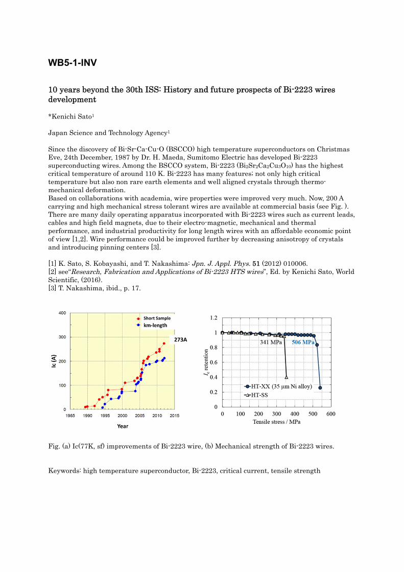
WB5-1-INV 10 years beyond the 30th ISS: History and future prospects of Bi-2223 wires development *Kenichi Sato1 Japan Science and Technology Agency1 Since the discovery of Bi-Sr-Ca-Cu-O (BSCCO) high temperature superconductors on Christmas Eve, 24th December, 1987 by Dr. H. Maeda, Sumitomo Electric has developed Bi-2223 superconducting wires. Among the BSCCO system, Bi-2223 (Bi2Sr2Ca2Cu3O10) has the highest critical temperature of around 110 K. Bi-2223 has many features; not only high critical temperature but also non rare earth elements and well aligned crystals through thermo-mechanical deformation. Based on collaborations with academia, wire properties were improved very much. Now, 200 A carrying and high mechanical stress tolerant wires are available at commercial basis (see Fig. ). There are many daily operating apparatus incorporated with Bi-2223 wires such as current leads, cables and high field magnets, due to their electro-magnetic, mechanical and thermal performance, and industrial productivity for long length wires with an affordable economic point of view [1,2]. Wire performance could be improved further by decreasing anisotropy of crystals and introducing pinning centers [3]. [1] K. Sato, S. Kobayashi, and T. Nakashima: Jpn. J. Appl. Phys. 51 (2012) 010006. [2] see“Research, Fabrication and Applications of Bi-2223 HTS wires”, Ed. by Kenichi Sato, World Scientific, (2016). [3] T. Nakashima, ibid., p. 17.
Fig. (a) Ic(77K, sf) improvements of Bi-2223 wire, (b) Mechanical strength of Bi-2223 wires. Keywords: high temperature superconductor, Bi-2223, critical current, tensile strength
WB5-2-INV 10 Years Beyond the 30th ISS: History and Future Prospects of Bi-2212 Conductors *Eric E. Hellstrom1, Ernesto S. Bosque1, Griffin Bradford1, Michael Brown1, Daniel S. Davis1, Charles L. English1, David K. Hilton1, Imam S. Hossain1, Jianyi Jiang1, Fumitake Kametani1, Youngjae Kim1, David C. Larbalestier1, Jun Lu1, Evan Miller1, George E. Miller1, Yavuz Oz1, Ulf P. Trociewitz1 Applied Superconductivity Center, National High Magnetic Field Laboratory, Florida State University, USA1 Bi-2212 was the first high temperature superconductor that demonstrated high-Jc in high-magnetic field. This was in 1989, but, it wasn’t until 2014 that Bi-2212 became a viable long-length conductor when overpressure (OP) processing was applied. OP processing removes the large, current limiting bubbles in powder-in-tube round wire. Bi-2212 is the HTS material that can be produced as a round wire, which gives it many advantages, including: it can be made in long lengths (BOST has drawn 2400 m long 0.8 mm diameter single piece lengths), it can be used as a round wire, or it can rolled to a slightly aspected rectangular shape, which are both geometries magnet designers and builders prefer; it can be cabled (Rutherford and twist cables, such as 6-on-1), it can be made with a wide variety of multifilament wire architectures, it can be twisted and transposed, and it is electromagnetically isotropic. With OP processing, Jc in short length wire samples is now 6860 A/mm2 (4.2 K, 15 T). Challenges for using Bi-2212 wire in magnets are that it has to be used in a wind and react magnets, it requires an OP heat treatment (~900 °C, 50 atm total pressure), the wire is mechanically weak, and the wire is expensive. Methods to deal with these challenges are being developed. We have OP processed a variety of single strands, cabled conductors, and coils made with single strand and with Rutherford cable for the Bi-2212 community. Future applications for Bi-2212 coils are in high-field NMR magnets, in accelerators for high-energy physics, and as replacement inserts in existing LTS laboratory magnets to upgrade the field achievable in these magnets. Keywords: Bi-2212, High temperature superconductors, High-field magnet, Round wire conductor
WB5-3-INV History and future prospects of MgB2 and iron based superconducting wires *Hiroaki Kumakura1 National Institute for Materials Science1
MgB2 wires have been developed by applying powder in tube(PIT) method and Internal Mg diffusion (IMD) method. One of the key factors that govern Jc values of MgB2 wires is the MgB2 core density. Applications of high pressure such as hot pressing, cold pressing and hot isostatic pressing have been successfully carried out to increase the MgB2 core density and Jc values. However, these methods are not practical for large scale fabrication of MgB2 wires. Other effective methods to increase MgB2 core density and Jc values are mechanical milling of Mg and B powder mixture and mechanical working with swaging. IMD process has also been studied and higher MgB2 layer density and higher Jc values than those of PIT wires are realized. However, Jc(Je) values of all these MgB2 wires are still not high enough for applications at around 20K and ~5T. Much higher Jc values of MgB2 thin films suggests that practical level Jc(Je) values can be realized by reducing the MgB2 grain size, eliminating impurity phases and introducing pinning centers.
Among various iron-based superconductors, (Ba(Sr),K)Fe2As2(Ba(Sr)-122) are potentially useful for high field(>25T) applications due to their high Bc2 over 50T and small anisotropy. Ba(Sr)-122 wires have been fabricated with ex situ PIT method. Besides Ba(Sr)-122 core density, c-axis grain orientation seems to be another key factor for high Jc values. Applications of high pressure improve the core density and c-axis grain orientation. Mechanical working with hard sheath materials is also effective in increasing the core density and c-axis grain orientation. However, present Ba(Sr)-122 wires show lower Jc-B properties than those of high-Tc oxide superconducting wires. Further increase of Ba(Sr)-122 core density, refinement of grain boundaries and introduction of pinning centers will realize practical level Jc values at high fields.
WB6-1-INV Recent results on flux pinning in nanoparticle-doped REBa2Cu3Oy Coated Conductor by TFA-MOD *Masashi Miura1, Michio Sato1, Takeharu Kato2, Tomohiro Kato2, Ryoji Yoshida2, Koichi Nakaoka3, Teruo Izumi3 Seikei University1 Japan Fine Ceramics Center2 National Institute of Advanced Industrial Science and Technology3 Nanostructural modifications, in particular nanoparticle additions, have been shown to have great success in improving Superconducting material performance, such as REBa2Cu3Oy (REBCO) superconducting films [1-3] and iron pnictide films [4]. For REBCO coated conductors (CCs), NPs disrupt the superconducting parameter locally while maintaining crystallinity unperturbed elsewhere, thus pinning vortices at the NPs and therefore preventing dissipation. To be effective, the NP size has to be tuned, and the density needs to be higher for greater enhancement. We show how an economically viable method, namely trifluoroacetate metal organic deposition (TFA-MOD), can be tuned to obtain both small size and high density of NPs while maintaining the crystallinity of the REBCO matrix. We achieve these goals in two ways: by changing the nanoparticle material and by modulating the precursor chemistry with the result of constraining the NPs spatially. We get significant improvement of the in-field critical current density (Jc) for NP-doped REBCO CCs over a broad temperature range. The enhancements are seen not only in Jc but also in the reduction of the effects of thermal fluctuations (flux creep) at all magnetic fields measured. Detailed microstructural and superconducting properties for nanocomposite REBCO CCs will be presented. Acknowledgements: M.M. is supported by JSPS KAKENHI (17H03239 and 17K18888). A part of this work was supported by a research grant from the Japan Power Academy. Reference: [1] J. Gutiérrez, J. et al. Nature Mater. 6 (2007) 367-373. [2] B. Maiorov, et al., Nature Mater. 8, (2009) 398. [3] M. Miura et al., Scientific Reports, 6 (2016) 20436. [4] M. Miura et al., Nature Commun. 4 (2013) 2499 Keywords: Critical Current, Nanoparticles, Pinning, TFA-MOD
WB6-2-INV Fast PLD growth of nanostructured YBCO coated conductors with artificial pinning centers Max Sieger1, Patrick Pahlke1, Jens Hänisch2, Mayraluna Lao2,3, Michael Eisterer3, Alexander Meledin4, Gustaaf Van Tendeloo4, Kornelius Nielsch1, Ludwig Schultz1, *Ruben Hühne1 Institute for Metallic Materials, IFW Dresden, Germany1 Institute for Technical Physics, Karlsruhe Institute of Technology, Germany2 Atominstitut, TU Wien, Vienna, Austria3 EMAT, University of Antwerp, Belgium4 YBa2Cu3O7-x (YBCO) and related compounds are promising materials for magnet and energy applications. The required flexible conductors are realized with the coated conductor technology using biaxially textured templates. More recently, significant efforts are devoted to enhance the current transport capability of the superconducting layers in magnetic fields by nano-engineering the microstructure using artificial pinning centers (APC) with an optimized size, density and distribution. We prepared thick YBCO layers using PLD with a typical growth rate above 1 nm/s on industrially fabricated biaxially textured templates incorporating additional APC such as BaHfO3 and the mixed double-perovskite Ba2Y(Nb/Ta)O6. Detailed TEM studies revealed size and distribution of the nanoparticles in dependence of the growth parameters showing typically a combination of a-b-oriented platelets and c-axis aligned nanorods. A critical current density Jc of up to 2 MA/cm2 was determined at 77 K in self-field for 1 µm thick films. Electrical transport property measurements showed a reduced Jc anisotropy in magnetic fields for the doped samples. We will discuss how the anisotropy might be tuned on the textured templates by the deposition conditions and the resulting distribution of the APC. Additionally, nanocomposite YBCO films with a thickness of up to 7 µm were grown on these templates. The incorporation of APC leads to a denser microstructure and a reduction of misoriented YBCO grains. We found that the influence of the granularity is significantly reduced in particular for RABiTS-based conductors. Nevertheless, a strong increase of a-axis oriented YBCO grains was observed for films with a thickness above 5 µm reducing the overall Jc values. The authors acknowledge financial support from EUROTAPES, a collaborative project funded by the European Union's Seventh Framework Programme (FP7 / 2007 - 2013) under Grant Agreement no. 280432. Keywords: YBCO coated conductors, pinning, PLD
WB6-3-INV Present status of High Performance REBCO Conductors and Recent Progress of Advanced MOCVD *Goran Majkic1,2,3,4 University of Houston1 Department of Mechanical Engineering2 Texas Center for Superconductivity3 Advanced Manufacturing Institute4 We present on recent progress and current status of high performance, high engineering current densities (Je) REBCO conductors. A substantial effort has been devoted towards improving the in-field performance of 2G-HTS conductors over a broad range of temperatures and fields via introduction of artificial pining centers, with particular focus on perovskite nanorods. We will present our recent progress in understanding the factors affecting BaZrO3 nanorod growth and their effect on in-field performance, leading to increasing the critical current density to 20 MA/cm2 at 30 K, 3 T. We will also present recent progress on Advanced MOCVD (A-MOCVD) reactor development, aimed at addressing the issues found in most superconductor deposition techniques such as a-axis grain formation, degradation of texture in thick films and poor precursor conversion efficiency. The progress is demonstrated by growing 4.8µm thick, BZO doped REBCO films in a single pass, achieving critical currents of 8705, 5586 and 3606 A/12mm at 3 T (B||c) and 30, 40 and 50 K, respectively, and corresponding Je of 7068, 4535 and 2928 A/mm2, which is a factor of ~7x higher than that of typical commercial HTS tapes with 7.5 mol% Zr addition. Such performance in thick films is a demonstration that growing thick REBCO films with high critical current density (Jc) in high magnetic fields is possible, contrary to the usual findings of strong Jc degradation with film thickness. This work is supported by the U.S. Department of Energy Advanced Manufacturing Office, Office of High Energy Physics and the Office of Naval Research
WB6-4-INV Progress in low cost chemical solution Nanocomposite YBa2Cu3O7-x coated conductors *Teresa Puig1, Ziliang Li1, Cornelia Pop1, Natalia Chamorro1,2, Bohores Villarejo1, Flavio Pino1, Ferran Vallés1, Bernat Mundet1, Laia Soler1, J. Jareño1, Silvia Rasi1,3, J. Banchewski1, R. Guzmán1, J. Gázquez1, M. Coll1, A. Palau1, S. Ricart1, J. Ros2, J. Farjas3, P. Roura3, X. Obradors1 Institut de Ciència de Materials de Barcelona, ICMAB-CSIC Campus de la UAB, 08193 Bellaterra, Spain1 Departament de Química, Universitat Autonoma de Barcelona, Campus UAB, 08193 Bellaterra, Spain2 GRMT, Department of Physics, University of Girona, E17071-Girona, Spain3 High current superconducting wires for large scale applications and magnets has been one of the most challenging achievements during all the HTS era. Coated conductors of YBa2Cu3O7 (YBCO) have emerged as the most attractive opportunity to reach unique performances while reducing the cost/performance ratio continues to be a key objective at present. Chemical solution deposition (CSD) is a very competitive cost-effective technique which has been used to obtain nanocomposite films and CCs. In the recent years we have been able to demonstrate the unique potentiality of these CSD techniques to achieve low cost, low anisotropy and high critical current coated conductors. In my presentation, I will report on the present understanding of growth process and vortex pinning of CSD nanocomposite YBCO films, obtained from complex solutions where the nanoparticles are spontaneously segregated during growth and the novel strategy using colloidal solutions of preformed oxide nanoparticles (NPs) stabilized in the YBCO precursor solutions. A thorough investigation correlating the pinning landscape with the defect microstructure has been pursuit with detailed angular dependent in-field critical currents and HRTEM/STEM analysis. I will also report on a new approach we are investigating based on low cost nanocomposite CSD crystallization through a transient-liquid assisted growth (TLAG) enabling ultrafast growth rates in the range of 50 nm/s. # This research has been funded by EU-ERC_AdG-2014-669504ULTRASUPERTAPE project, EU-FP7 NMP-LA-2012-280432 EUROTAPES project and Excellence Program Severo Ochoa SEV2015-0496 Keywords: CSD, Nanocomposites growth, vortex pinning, films and coated conductors
WB6-5-INV High performance REBa2Cu3Oy coated conductors with designed artificial pinning center *Yutaka Yoshida1, Yusuke Ichino1, Yuji Tsuchiya1, Kaname Matsumoto2, Teruo Izumi3, Ataru Ichinose4, Satoshi Awaji5 Nagoya university1 Kyushu Inst. Tech2 AIST3 CRIERI4 Tohoku university5 We study to determineabout optimum shapes of the artificial pinning center (APC) of REBa2Cu3Oy (REBCO) coated conductors towards superconducting magnets operating at temperatures of 77 K or less.and lower temperature. Superconducting properties have been changedvary depending on the by different kind and addition amountquantity of BaMO3 added to REBCO. Therefore, we study the changes in theof shapes of nanorods that areshape due to the difference in theof nature of additives and growth temperature. In addition, weand aim to control the APC having anwith the optimum shape that matchesing the operating temperature. The high flux pinning performance was obtained for a 3.8vol.% BaHfO3 (BHO)-doped SmBa2Cu3Oy (SmBCO) on IBAD-MgO. At 77.3 K, the irreversibility field (Birr) of 16.8 T and the maximum flux pinning force density (Fp) of 32.5 GN/m3 (B//c) were achieved. In addition, the maximum Fp values of 400 GN/m3 and 120 GN/m3 for B//c were realized at 40 K and 65 K. In particular, we describe the shape control of nanorods in SmBCO coated conductors by employingusing low temperature growth (LTG) technology using seed layers. From the cross- sectional TEM observations, weit was confirmed that using the LTG technique, the BHO nanorods, which were comparatively thin in diameter and short in length, formed athe fireworks structure in the case of SmBCO coated conductors. using the LTG method. The superconducting properties in the magnetic field of the SmBCO- coated conductor on IBAD-MgO with the optimum amount of BHO showed that Fpmax = 1.5 TN / m 3 at 4.2K. On the other hand, the high-speed growth technique for high performance SmBCO coated conductor is an important subject. In this presentation, we will describe the development of the coated conductor fabricated with a repetition rate of 100 Hz, changed from 10 Hz. We will discuss the details of microstructures and superconducting properties of BHO nanorods in SmBCO coated conductor using the laser system with high repetition rate. This work was partly supported by a Grant-in-Aid for Scientific Research (15H04252 and 16H04512). A part of this work includes the results supported by the ALCA project of the Japan Science and Technology Agency (JST) and NU-AIST alliance project. Keywords: flux pinning, artificial pinning center, microstructure, nanorod
WB6-6-INV Analysis and Modeling of Current Transport Properties in Long Length Coated Conductors *Takanobu Kiss1, Kohei Higashikawa1, Takumi Suzuki1, Yuhei Nishimiya1, Yuta Onodera1, Masayoshi Inoue1, Mitsunori Igarashi2, Kazuomi Kakimoto2, Yasuhiro Iijima2 Dept. of Electrical Engineering, Kyushu University, Fukuoka 819-0395, Japan1 Fujikura Ltd. Sakura 285-8550, Japan2 Current-Voltage (I-V) characteristic is one of the most fundamental properties of superconducting materials for practical applications. While the I-V characteristics are usually measured by using a short piece sample and/or a micro-bridge, practical applications require long length tapes in hundreds of meters to several kilo-meters. Spatial homogeneity becomes an important issue in such cases because the minimum Ic will limit the total performance of the full-length of the tape. Therefore, Ic in the long length tape has been studied significantly as a function of longitudinal coordinate. However, it is not yet fully understood the relationship between the local Ic variation and the global I-V characteristics. In this study, we have investigated current transport properties in long length coated conductors (CCs) based on coupled analysis using reel-to-reel high-speed scanning Hall probe microscopy and site-specified transport measurements. An analytical model to describe the relationship between the local Ic variation and the global I-V characteristics in such long length CCs have been proposed. Furthermore, we will discuss a method to increase reliability, robustness and current carrying capability of the CCs under the influence of spatial Ic variation. Acknowledgements: This work was supported by “JSPS KAKENHI (16H02334)” and “NEDO”. Keywords: critical current, current transport, coated conductor, modeling
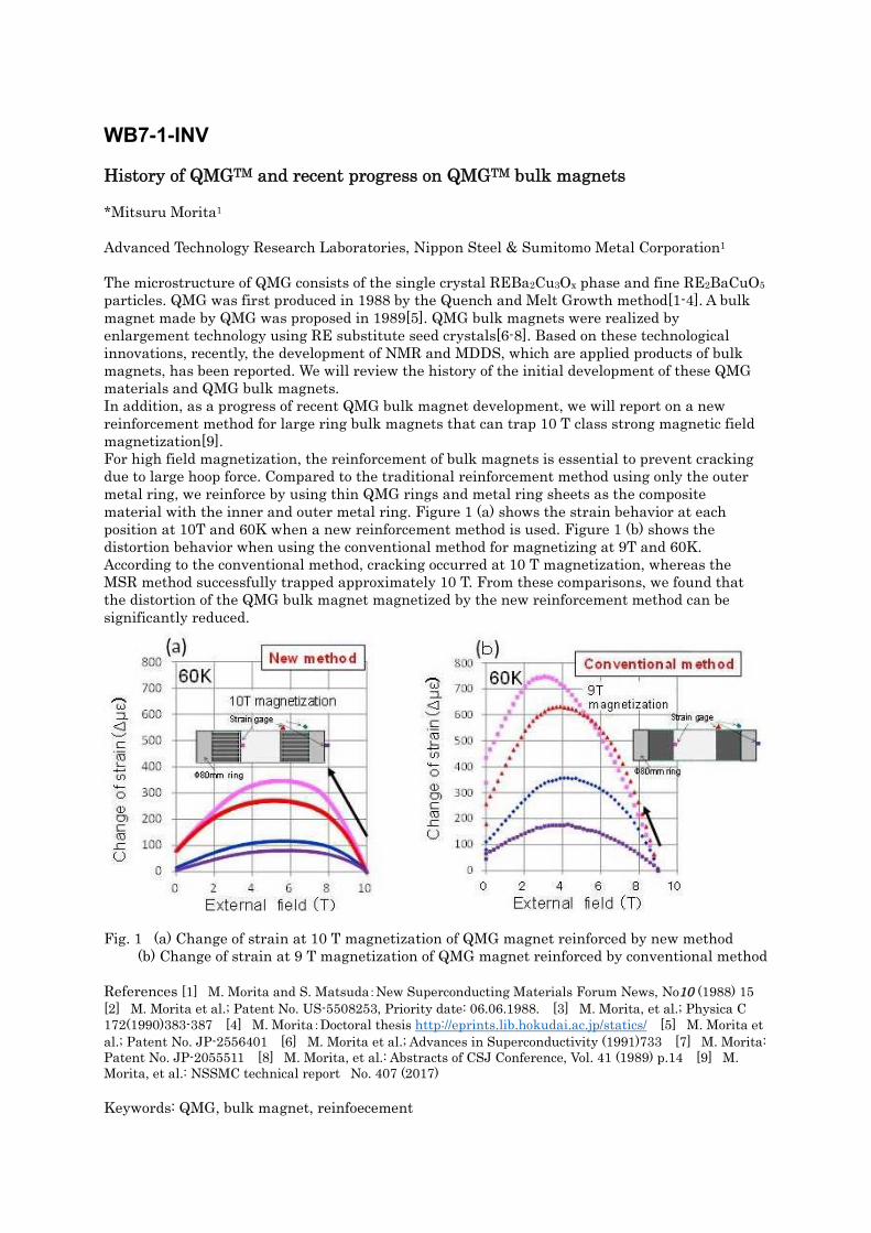
WB7-1-INV History of QMGTM and recent progress on QMGTM bulk magnets *Mitsuru Morita1 Advanced Technology Research Laboratories, Nippon Steel & Sumitomo Metal Corporation1 The microstructure of QMG consists of the single crystal REBa2Cu3Ox phase and fine RE2BaCuO5 particles. QMG was first produced in 1988 by the Quench and Melt Growth method[1-4]. A bulk magnet made by QMG was proposed in 1989[5]. QMG bulk magnets were realized by enlargement technology using RE substitute seed crystals[6-8]. Based on these technological innovations, recently, the development of NMR and MDDS, which are applied products of bulk magnets, has been reported. We will review the history of the initial development of these QMG materials and QMG bulk magnets. In addition, as a progress of recent QMG bulk magnet development, we will report on a new reinforcement method for large ring bulk magnets that can trap 10 T class strong magnetic field magnetization[9]. For high field magnetization, the reinforcement of bulk magnets is essential to prevent cracking due to large hoop force. Compared to the traditional reinforcement method using only the outer metal ring, we reinforce by using thin QMG rings and metal ring sheets as the composite material with the inner and outer metal ring. Figure 1 (a) shows the strain behavior at each position at 10T and 60K when a new reinforcement method is used. Figure 1 (b) shows the distortion behavior when using the conventional method for magnetizing at 9T and 60K. According to the conventional method, cracking occurred at 10 T magnetization, whereas the MSR method successfully trapped approximately 10 T. From these comparisons, we found that the distortion of the QMG bulk magnet magnetized by the new reinforcement method can be significantly reduced.
Fig. 1 (a) Change of strain at 10 T magnetization of QMG magnet reinforced by new method (b) Change of strain at 9 T magnetization of QMG magnet reinforced by conventional method References [1] M. Morita and S. Matsuda:New Superconducting Materials Forum News, No10 (1988) 15 [2] M. Morita et al.; Patent No. US-5508253, Priority date: 06.06.1988. [3] M. Morita, et al.; Physica C 172(1990)383-387 [4] M. Morita:Doctoral thesis http://eprints.lib.hokudai.ac.jp/statics/ [5] M. Morita et al.; Patent No. JP-2556401 [6] M. Morita et al.; Advances in Superconductivity (1991)733 [7] M. Morita: Patent No. JP-2055511 [8] M. Morita, et al.: Abstracts of CSJ Conference, Vol. 41 (1989) p.14 [9] M. Morita, et al.: NSSMC technical report No. 407 (2017) Keywords: QMG, bulk magnet, reinfoecement
WB7-2-INV Collecting Ni-Sulfate Compound from Electroless Plating Waste by Magnetic Separation Technique with Use of HTS Bulk Magnets *Tetsuo Oka1, Sho Sasaki1, Hideto Sasaki1, Satoshi Fukui1, Jun Ogawa1, Takao Sato1, Tomohito Nakano1, Manabu Ooizumi1, Morio Tsujimura2, Kazuya Yokoyama3 Niigata University, Japan1 Aichi Giken Co., Japan2 Ashikaga Institute of Technology, Japan3 The authors have developed a useful technique for extracting the Ni-sulfate compound from the waste fluid of the electroless Ni-plating processes. The plating waste still contains the Ni ions with high concentration even after the several plating cycles. After forming the fine NiHPO3 precipitate from the waste, the coarse NiSO4 crystals were synthesized through the reaction with the concentrated sulfuric acid. In the experiment, the open-gradient magnetic separation was employed to collect the NiSO4 crystals from the muddy mixture composed of these compounds due to the difference between their magnetic properties. The experiments were practically conducted with use of the Gd123-based HTS bulk magnets generating up to 4 T with the steep gradient of magnetic field, which were activated by the field cooling magnetization process operated at 35 K. The ratio of NiSO4 content in the slurry attracted to the magnetic pole has reached up to 85.7%. This preferential collection suggests a feasible recycling system of Ni resource as a raw material in the plating processes. Keywords: high Tc superconductor, bulk magnet, magnetic separation, nickel plating
WB7-3 SmBCO single grain bulk superconductors via Top seeded infiltration and growth process Devendra K Namburi1, Wen Zhao1, Yunhua Shi1, Anthony R Dennis1, John H Durrell1 and David A Cardwell1 Department of Engineering, University of Cambridge, Cambridge CB2 1PZ, UK1 (RE)-Ba-Cu-O bulk superconductors in single grain form can trap magnetic fields which are an order of magnitude higher compared to the conventional permanent magnets and hence are attractive for a variety of engineering and technological applications. In the present work, the fabrication procedure of SmBCO single grain superconductors via Top seeded infiltration and growth (TSIG) technique is presented. The TSIG approach results in near-net shaped dense SmBCO products. The superconducting and microstructural properties of single grain SmBCO bulk superconductors obtained by the TSIG technique will be presented. Acknowledgements: This work was supported by King Abdulaziz City for Science and Technology (KACST) and the Engineering and Physical Sciences Research Council (EPSRC, grant number EP/K02910X/1).
WB7-4 How to Control the Gd211 Particles and Enhance the Levitation Force of Single Domain GdBCO Bulks Prepared by Gd+011 TSIG Method *Wanmin Yang1, Xiaochun Yuan1, Chunyan Zhang1 Department of Physics, Shaanxi Normal University, Xi'an, Shaanxi, 710062, China,1 The empirical evidences have indicated that the new RE+011 TSIG method is a very effective method for fabrication of high quality REBCO bulk superconductors, because of strong flux pinning force by the uniformly distributed unknown nanometer particles. But there are still many larger size RE211 particles in the REBCO bulks. To overcome this problem, a sires single domain GdBCO bulk superconductors have been prepared with different solid phase pellets sintered at different temperature (T) by the Gd+011 TSIG method, the results indicate that: (1) The average size of Gd211 particles in precursor solid phase pellets is monotonously increasing from nanometer to 4.23 μm with increasing of the sintering temperature up to 1200 ℃. (2) The density of the precursor solid phase pellets increases with the increasing T when T is great than 950 ℃, but the density is lower than that of the as pressed pellets when T is less than 1000 ℃. (3) The average size of Gd211 particles in the single domain GdBCO bulks first decreases from 10.9 μm to 2.81 μm and then increases from 2.81 μm to 3.96 μm with increasing T, and the smallest Gd211 particles 2.81 μm is obtained in the sample sintered at 1050 ℃; this is much different from the result of the samples prepared by the traditional TSIG process. (4) The maximum levitation force 38 N (77 K, 0.5 T) is obtained in the sample with a relatively larger size of Gd211 particles and higher density, but not achieved in the sample with the smallest Gd211 particles. In order to further improve the quality of single domain GdBCO bulk samples, another sires of single domain GdBCO bulk superconductors have also prepared with solid phase pellets sintered at 1000 ℃ with different times by Gd+011 TSIG method, the results indicate that: the levitation force of the samples firstly increases from 37 N to 51 N when the t increases from 10 h to 15 h and then decrease to 16 N when the t further increases to 30 h. The largest levitation force 51 Nis about 38% higher than that of the best samples mentioned above. This result provides a very effective way to fabricate high quality REBCO bulk superconductors by control the density, RE211 particle size and their distributions in the solid phase pellets. Keywords: single domain GdBCO bulk superconductors, Gd+011 TSIG method, Gd211 particles, density of solid phase pellet
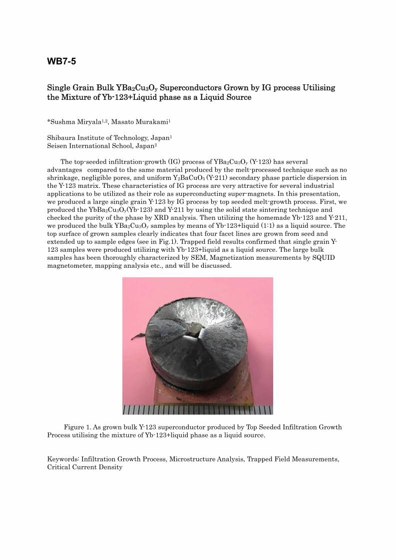
WB7-5 Single Grain Bulk YBa2Cu3Oy Superconductors Grown by IG process Utilising the Mixture of Yb-123+Liquid phase as a Liquid Source *Sushma Miryala1,2, Masato Murakami1 Shibaura Institute of Technology, Japan1 Seisen International School, Japan2 The top-seeded infiltration-growth (IG) process of YBa2Cu3Oy (Y-123) has several advantages compared to the same material produced by the melt-processed technique such as no shrinkage, negligible pores, and uniform Y2BaCuO5 (Y-211) secondary phase particle dispersion in the Y-123 matrix. These characteristics of IG process are very attractive for several industrial applications to be utilized as their role as superconducting super-magnets. In this presentation, we produced a large single grain Y-123 by IG process by top seeded melt-growth process. First, we produced the YbBa2Cu3Oy(Yb-123) and Y-211 by using the solid state sintering technique and checked the purity of the phase by XRD analysis. Then utilizing the homemade Yb-123 and Y-211, we produced the bulk YBa2Cu3Oy samples by means of Yb-123+liquid (1:1) as a liquid source. The top surface of grown samples clearly indicates that four facet lines are grown from seed and extended up to sample edges (see in Fig.1). Trapped field results confirmed that single grain Y-123 samples were produced utilizing with Yb-123+liquid as a liquid source. The large bulk samples has been thoroughly characterized by SEM, Magnetization measurements by SQUID magnetometer, mapping analysis etc., and will be discussed.
Figure 1. As grown bulk Y-123 superconductor produced by Top Seeded Infiltration Growth Process utilising the mixture of Yb-123+liquid phase as a liquid source. Keywords: Infiltration Growth Process, Microstructure Analysis, Trapped Field Measurements, Critical Current Density
WB8-1-INV Development of RE123 and MgB2 Superconducting Bulk Magnets *Atsushi Ishihara1, Tomoyuki Akasaka1, Taiki Onji1, Yusuke Fukumoto1, Masaki Sekino2, Hiroyuki Ohsaki2, Kohji Kishio2, Toshiteru Kii3, Masaru Tomita1 Railway Technical Research Institute1 The University of Tokyo2 Kyoto University3 Since the discovery of high temperature superconductors in 1986, superconducting materials come in a variety of forms, not only in wire forms but also in bulk forms [1]. Especially, high temperature superconducting bulk magnets, REBa2Cu3Oy (RE123) and MgB2, generate strong magnetic field in compact size [2-4], since superconducting bulks have high critical current density under up to high magnetic fields. Once bulks are magnetized, magnetic field by the superconducting current is maintained because of strong pinning and bulks work as strong permanent magnets under the cooling condition. In other word, superconducting bulks are regarded as bulk-shape coils which consist of superconducting wires connected with perfect superconducting joints. In this presentation, conditions and outlook of high temperature superconducting bulks, RE123 and MgB2 bulks, are discussed by comparison. Specifically, RE123 and MgB2 bulk magnets were fabricated and, local and global magnetic properties of these bulks were evaluated to investigate the possibility that superconducting bulks have the potential as a powerful magnet [5]. Furthermore, homogeneity of trapped magnetic field in radial and circumferential directions which is very important for equipment design was also evaluated. Acknowledgements This work was partly supported by JSPS KAKENHI Grant Number JP 16H01860 and JP 17H01127. References [1] G. Krabbes et. al., “High Temperature Superconductor Bulk Materials: Fundamentals, Processing, Properties Control, Application Aspects.” Wiley-VCH (2006). [2] M. Tomita and M. Murakami, Nature 421 (2003) 517. [3] J. Durrell et. al., Supercond. Sci. Technol. 27 (2014) 0820001. [4] M. Tomita et al., Abstracts of CSSJ Conference 83 p.86 (2010) [5] A. Ishihara et. al., Supercond. Sci. Technol. 30 (2017) 035006. Keywords: superconducting bulk, RE123, MgB2, trapped magnetic field
WB8-2-INV Record critical current density in sintered MgB2 bulks *Muralidhar Miryala1, Masaki Higuchi1, Miles Jirsa2, Michael R Koblischka3, Masato Murakami1 Shibaura Institute of Technology1 Institute of Physics ASCR2 Saarland University3 To utilize any material in daily-life applications requires a low cost production together with high performance. This applies also for bulk superconducting magnets. In this invited presentation, we will introduce the production route of MgB2 bulks by a simple sintering solid state reaction technique, which is appropriate for batch production. We prepared several sets of MgB2 bulks from commercial high-purity powders of Mg metal and carbon-coated amorphous B using a single-step, solid-state reaction process. Some of the samples were rapidly quenched from the sintering temperature of 800 °C down to liquid nitrogen temperature at different stages of the sintering duration (1-5 h). To improve the flux pinning and the mechanical performance of the material, the bulks were produced from Mg-rich MgB2 material with addition of 1.5 wt.-% carbon-coated, amorphous B powder combined with 4 wt.-% of silver. All samples were characterized by x-ray diffraction and scanning electron microscopy. The superconducting performance, Tc, and the critical current, Jc, at 20 K were accessed by means of SQUID magnetometry. The Jc values in Mg-rich MgB2 material with 4 wt.-% of Ag were higher than in silver-free MgB2 bulks. The sample with 4 wt.-% Ag combined with 1.5 wt.-% of carbon-coated B exhibited the highest Jc of 5.2 × 10⁵ A/cm2 at 20 K and self-field. The MgB2 sample sintered for 3 h and quenched to LN2 showed superior Jc values of 5 × 10⁵ A/cm2 and a sharp superconducting transition with Tc (onset) at 38.1 K. This Jc value is twice as high as that of the pure sample, the best value reported so far. Our results demonstrate a strong correlation between the microstructure achieved and the resulting pinning performance. Keywords: MgB2, x-ray diffraction , SEM and AFM, Critical Current Density
WB9-1-INV An Intermediate Grown Superconducting (iGS) Joint between REBCO Coated Conductors: Fabrication, Microstructure and Superconducting Properties *Kotaro Ohki1, Tatsuoki Nagaishi1, Takashi Yamaguchi1, Yoshinori Yanagisawa2, Renzhong Piao2, Hideaki Maeda2, Takeharu Kato3, Daisaku Yokoe3, Tsukasa Hirayama3, Yuichi Ikuhara3,4, Hitoshi Kitaguchi5, Takeshi Ueno6, Kazama Yamagishi6, Tomoaki Takao6 Sumitomo Electric, Japan1 RIKEN, Japan2 Japan Fine Ceramics Center, Japan3 University of Tokyo, Japan4 National Institute for Materials Science, Japan5 Sophia University, Japan6 Over the past few years, several studies have been performed on the superconducting joint of REBa2Cu3Oy (REBCO, RE: rare earth elements) coated conductors (CCs) which is one of the key technologies to realize persistent current operations of prominent HTS magnets [1, 2]. Park has succeeded in the superconducting joint of REBCO CCs [1]. However, the total processing time is too long for large coil applications such as nuclear magnetic resonance (NMR) and magnetic resonance imaging (MRI). We have developed a novel superconducting joint technology for REBCO CCs. It uses a joining strap with a microcrystalline REBCO precursor layer. The joint technology has an advantage of a sufficiently short total processing time of less than one day. The joining strap and the GdBCO CCs were heated at 800 °C for 20 min. in an atmosphere of 100 ppm oxygen to make the polycrystalline GdBCO on the joining strap grow epitaxially. This intermediate grown superconducting (iGS) joint gives a critical current of > 100 A at 77 K in a self-field. Cross sectional investigation of the joint area was carried out by a scanning electron microscope (SEM) and a transmission electron microscope (TEM). An SEM image indicates that there are some voids and inclusions, such as CuO and Gd2O3, in the joint area. In spite of the voids and the inclusions, approximately 60% of the superconducting layers were directly connected. Furthermore, a high resolution image obtained by the TEM shows that the microcrystal grows epitaxially and the boundary of the GdBCO layers of the CCs and the GdBCO layer of the joining strap were atomically connected with the grown intermediate layer. It was estimated from the persistent field decay curve that a joint resistance was in the order of 10-12–10-13 at 77 K in a self-field over three days, with an operating current of ∼10 A (∼14% of the calculated coil critical current). In this presentation, the magnetic field dependence of the critical current will be shown. We believe the superconducting joint technology is promising for realization of the persistent current mode operation of NMR and MRI. [1] Park Y, Lee M, Ann H, Choi Y H and Lee H 2014 NPG Asia Materials 6 e98. [2] Jin X, Yanagisawa Y, Maeda H and Takano Y 2015 Supercond. Sci. Technol. 28 75010. Keywords: REBCO-coated conductor, superconducting joint, microcrystalline precursor intermediate, microstructure
WB9-2-INV Superconducting joint of REBCO wires for MRI magnet *Shinichi Mukoyama1, Akinobu Nakai1, Hisaki Sakamoto1, Shinji Matsumoto2, Gen Nishijima2, Mamoru Hamada3, Kazuyoshi Saito3, Yasuyuki Miyoshi3 Furukawa Electric Co., Ltd.1 National Institute for Materials Science2 Japan Superconductor Technology, Inc.3 High temperature superconducting wires (HTS wires) are promising for superconducting magnet applications because it is operated at higher temperature than liquid helium temperature. Particularly, a MRI magnet using the HTS wires is expected to obtain light-weight, compact and low operation cost. The HTS MRI magnet needs a technology of the persistent current mode. However, a superconducting joint of HTS wires has not been realized stably at this time. We have developed a superconducting joint by using commercial REBCO tapes, and the superconducting joint with 10-12 ohm and 100 A-class was achieved by a direct-contact between superconducting layers of two REBCO wires. Moreover, a measurement equipment of low joint resistance was developed by measuring decays of magnetic field in the one-turn-loop that consisted of a REBCO wire and a superconducting joint. Keywords: REBCO wire, superconducting joint, persistant current mode, MRI magnet
WB9-3-INV Magnetic Field Stability in the Persistent Current Operation of the REBCO Coil with a Superconducting Joint *K. Takahashi1, T. Hase1, S. Awaji1, A. Nakai2, S. Yamano2, H. Sakamoto2 Institute for Materials Research, Tohoku University, Sendai 980-8577, Japan1 Furukawa Electric Co., Ltd., Ichihara 290-8555, Japan2 HTS superconducting magnets for MRI and NMR should be operated in a persistent current mode in order to achieve high temporal stability of the magnetic field of less than 1 ppm/h. Persistent current operation techniques of an HTS coil, however, have not been established yet. A persistent current switch (PCS) and a superconducting joint are the key technologies for persistent current operation. Recently, Furukawa Electric Co., Ltd. has successfully developed the superconducting joint technology with a resistance on the order of 10-12 Ω and a PCS using REBCO tapes, connected with a REBCO double pancake coil. In this paper, we report detail results of persistent operation tests of the system including a superconducting joint, a PCS and a pancake coil fabricated with a REBCO tape in a self-field and an external magnetic field of 1 T at 20 K. The persistent current system was fabricated with a SuperPower REBCO tape that had a dimension of 6 mm width and 0.1 mm thickness. The REBCO double pancake coil had 80 2 turns with the inner and outer diameters of 44 and 68 mm, respectively, and the inductance of 1.54 mH. The persistent current system was conduction-cooled by a 4K-GM cryocooler in the cryostat installed in a 220 mm room temperature bore of a cryogen-free superconducting magnet. The current decay behavior in persistent current operations up to 170 A were measured using a Hall probe located at the center of the coil. The decay rate of the magnetic field after five days operation was evaluated to be 1.7 ppm/h for the excitation current of 170 A in the self-field. The voltage-current characteristics obtained from decay curves of the magnetic field indicate that the decay behavior of persistent current are dominated by the joint resistance in 1 T but by the shielding current in the self field. Keywords: Persistent current operation, REBCO coil, Shielding current, Superconducting joint
WB9-4 Enhancement of Joint Properties of Various Ultrasonic Welded CC Joints *Hyung-Seop SHIN1, Chan Hun Jung1 Andong National University, Andong, 36729 Korea1 As a means to produce long-length high temperature superconducting wires with relatively uniform current capacity along its length, a new joining technology of 2G coated conductor (CC) tapes based on an ultrasonic welding (UW) was developed. The UW CC joining technique showed a good adhesion without any damage to the superconducting film layer and with an acceptable low joint resistance, making it reliable and reproducible. Recently, we attempted to achieve a low joint resistivity through the optimization of joining parameters for UW including horn tip patterns, an introduction of pre-Sn plating and a hybrid welding (HW) which incorporates soldering to the UW. Particularly, these methods are very effective for practical applications of CC joints using the UW technique because of its shorter welding time and in an easier way, and applicable to in-line process. The method can be satisfactorily applicable to various joint structures of lap- and butt-joint for Cu-stabilized CC tapes, and bridge joint for CC coils based on the UW process. In this study, in order to characterize the joint properties of the resistive CC joints fabricated by various joining methods, the joint resistivity and the electromechanical properties were evaluated at 77 K, respectively. The electromechanical testing was performed under both loading conditions of uniaxial tension and double bending at 77 K and self-field, respectively. The irreversible tension load limit and the minimum bending diameter against the retained Ic and joint resistance Rj degradation for various CC joints were determined, respectively, and the n value behaviors were also examined. This work was supported by a grant from National Research Foundation of Korea (NRF-2017-001109), funded by the Ministry of Science, ICT and Future Planning (MSIP), Republic of Korea. Keywords: coated conductor, ultrasonic welding, joint structure, electromechanical properties
WBP1-1 Improvement of uniformity of Ic distributions in long REBCO with BMO coated conductors by in-plume PLD method *Akira IBI1, Takato MACHI1, Koichi NAKAOKA1, Teruo IZUMI1 National Institute of Advanced Industrial Science and Technology (AIST)1 Long REBa2Cu3OX (REBCO, RE: rare earth element) with BaMO3 (BMO, M: metal) coated conductors have been expected for the industrial and commercial applications at high temperatures in magnetic fields. More recently, we fabricated long EuBa2Cu3OX (EuBCO) with BaHfO3 (BHO) coated conductors by the PLD method, which showed the high in-field Ic values of about 120 -140 A/cm-w at 77 K and 3 T [1]. However, in order to realize REBCO with BMO coated conductors for industrial and commercial applications, the much higher uniformity of not only longitudinal and but transversal Ic distributions of long coated conductors with high in-field performance is required. The in-plume PLD method is performed shortening the target-substrate distance to increase the deposition rate. However, it is difficult to control the deposited REBCO layer composition and the increased supersaturation for in-plume PLD method. To solve these problems, we used the Ba-deficient off-stoichiometric REBCO target and increase the number of multi-plume with scan of X-Y axes directions. Moreover, high uniformity of Ic distributions in long coated conductors by in-plume PLD method can be expected, since the deposition through the inside of multi-plume is less affected by change of plume conditions such as tilt and swing of plume. We have tried to develop the long EuBCO with BHO coated conductors by the in-plume PLD method with vapor-liquid-solid (VLS) mode [2] and high deposition rate of about 24 nm/s to obtain high in-filed performance and low production cost. As a result, we fabricated the long EuBCO with BHO coated conductors with high uniformity of Ic distributions by the in-plume PLD method comparing with coated conductors by the conventional PLD method. The detail of uniformity of Ic distributions and in-filed performance of long EuBCO with BHO coated conductors fabricated by in-plume PLD method will be discussed. This work was supported by the New Energy and Industrial Technology Development Organization (NEDO). [1] T. Yoshida et al, Physica C: Superconductivity 504 (2014) 42-46 [2] A. Ibi et al, Physics Procedia 81 (2016) 97-100 Keywords: PLD, long REBCO with BMO coated conductors, uniformity of Ic distributions
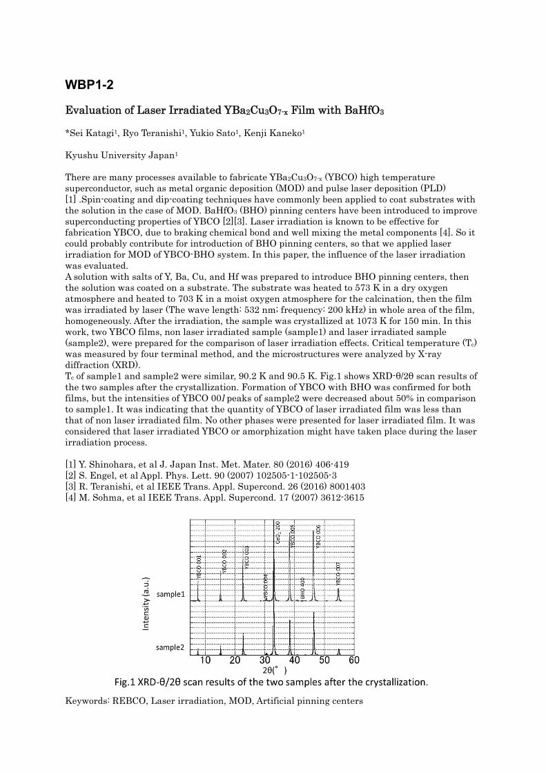
WBP1-2 Evaluation of Laser Irradiated YBa2Cu3O7-x Film with BaHfO3 *Sei Katagi1, Ryo Teranishi1, Yukio Sato1, Kenji Kaneko1 Kyushu University Japan1 There are many processes available to fabricate YBa2Cu3O7-x (YBCO) high temperature superconductor, such as metal organic deposition (MOD) and pulse laser deposition (PLD) [1] .Spin-coating and dip-coating techniques have commonly been applied to coat substrates with the solution in the case of MOD. BaHfO3 (BHO) pinning centers have been introduced to improve superconducting properties of YBCO [2][3]. Laser irradiation is known to be effective for fabrication YBCO, due to braking chemical bond and well mixing the metal components [4]. So it could probably contribute for introduction of BHO pinning centers, so that we applied laser irradiation for MOD of YBCO-BHO system. In this paper, the influence of the laser irradiation was evaluated. A solution with salts of Y, Ba, Cu, and Hf was prepared to introduce BHO pinning centers, then the solution was coated on a substrate. The substrate was heated to 573 K in a dry oxygen atmosphere and heated to 703 K in a moist oxygen atmosphere for the calcination, then the film was irradiated by laser (The wave length: 532 nm; frequency: 200 kHz) in whole area of the film, homogeneously. After the irradiation, the sample was crystallized at 1073 K for 150 min. In this work, two YBCO films, non laser irradiated sample (sample1) and laser irradiated sample (sample2), were prepared for the comparison of laser irradiation effects. Critical temperature (Tc) was measured by four terminal method, and the microstructures were analyzed by X-ray diffraction (XRD). Tc of sample1 and sample2 were similar, 90.2 K and 90.5 K. Fig.1 shows XRD-θ/2θ scan results of the two samples after the crystallization. Formation of YBCO with BHO was confirmed for both films, but the intensities of YBCO 00l peaks of sample2 were decreased about 50% in comparison to sample1. It was indicating that the quantity of YBCO of laser irradiated film was less than that of non laser irradiated film. No other phases were presented for laser irradiated film. It was considered that laser irradiated YBCO or amorphization might have taken place during the laser irradiation process. [1] Y. Shinohara, et al J. Japan Inst. Met. Mater. 80 (2016) 406-419 [2] S. Engel, et al Appl. Phys. Lett. 90 (2007) 102505-1-102505-3 [3] R. Teranishi, et al IEEE Trans. Appl. Supercond. 26 (2016) 8001403 [4] M. Sohma, et al IEEE Trans. Appl. Supercond. 17 (2007) 3612-3615
WBP1-3 3D Study of EuBa2Cu3Oy and GdBa2Cu3Oy Coated Conductors Using Focused Ion Beam-Scanning Electron Microscopy System Daisaku Yokoe1, Ryuji Yoshida1, *Takeharu Kato1, Akira Ibi2, Tsukasa Hirayama1, Teruo Izumi2 Nanostructures Research Laboratory, Japan Fine Ceramics Center1 Department of Energy and Environment, National Institute of Advanced Industrial Science and Technology2 EuBa2Cu3Oy (EuBCO) or GdBa2Cu3Oy (GdBCO) layers containing BaHfO3 (BHO) nanorods were deposited on HastelloyTM tapes with textured CeO2/LaMnO3/MgO/Y2O3/Gd-Zr-O buffer layers by PLD [1]. Nanostructures of these layers were characterized by scanning electron microscopy (SEM) and transmission electron microscopy. In addition, 3D reconstruction of the both EuBCO and GdBCO layers were performed using a focused ion beam-SEM system [2]. Both the EuBCO and the GdBCO layers were mainly composed of c-axis oriented EuBCO and GdBCO grains. The average diameter of the BHO nanorods was almost the same value in the both layers, which is 4.5 nm. In addition, outer growth EuBCO or GdBCO grains having different orientations compared with those of a matrix of c-axis oriented grains were formed. They were nucleated on CuO grains in the matrix and obstructed supercurrent. In the case of GdBCO layer, the outer growth grains were only seen near the GdBCO surface. On the other hand, Ba-Cu-oxides were found on the surface of c-axis oriented EuBCO grains. The Ba-Cu-oxides were considered to be a liquid phase during the PLD process, because those formed large droplet shape. In general, REBa2Cu3Oy (RE: rare earth) layers grow in a vapor-solid growth mode in the PLD process. However, the growth mode of the EuBCO layer would be changed from a vapor-solid to a vapor-liquid-solid mode at least within the PLD conditions (temperature, PO2 etc.) in this study, which was proved to some extent by existence of Ba-Cu-oxides on the surface [1,2]. The results of 3D reconstruction of the both layers indicated that the volume fraction of the outer growth grains in the matrix of the c-axis oriented EuBCO grains were much lower than that in the matrix of the GdBCO. In addition, the voids, which were found between the outer growth grains and the matrix of the GdBCO, were not confirmed in the EuBCO layer, and large Ba-Cu-oxides of a droplet morphology were distributed on the surface of the EuBCO layer [2]. A part of this research was supported by the Development of Medical Devices and Systems for Advanced Medical Services from the Japan Agency for Medical Research and development, AMED. [1] A. Ibi et al., Physics Procedia, 81, 97-100 (2016). [2] D. Yokoe et al., AMTC Letters, 5, 154-155 (2016). Keywords: 3D, FIB-SEM, PLD, Growth mode
WBP1-4 Apparent pinning potential of SmBCO superconducting thin film with BHO artificial pins *Kei Kashiwagi1, Masaru Kiuchi1, Teruo Matsushita1, Edmund Soji Otabe1, Yuji Tsuchiya2, Yutaka Yoshida2, Tadahiro Akune3, Terukazu Nishizaki3 Kyushu Institute of Technology, Japan1 Nagoya University, Japan2 Kyushu Sangyo University, Japan3 Introduction of artificial pins such as BaHfO3 (BHO) is effective for improving the high magnetic field characteristics of the critical current density Jc of oxide superconductors [1]. In particular, excellent Jc characteristics can be obtained when BHO is added. Therefore, SmBa2Cu3Oy (SmBCO) wire with BHO added as artificial pins is expected to be introduced into high magnetic field application such as MRI. Since this device will be commonly operated in the high uniformity magnetic field, a decay of superconducting current is required to be suppressed severely. Therefore, it is necessary to clarify the relaxation characteristics of Jc. In this study, in order to investigate the flux pinning characteristics of SmBa2Cu3Oy with BHO at high concentration, the relaxation characteristics of Jc were measured and the effect of artificial pin addition was investigated. The superconducting sample used in this study is a SmBCO thin film on which a superconducting layer was fabricated on the IBAD - MgO substrate by the PLD method. The artificial pin was added at 3 volume% BHO and 0 volume% without addition was also prepared. The thickness of the superconductor is d = 250 nm for both samples. Jc was evaluated from the magnitude of the magnetic moment and, U0* was evaluated from the time logarithmic relaxation rate of magnetization using a SQUID magnetometer. Figure 1(a) shows the magnetic field dependence of Jc. In the case of 3 volume% BHO showed a constant value in the measurement magnetic field range above 2 T with almost no degradation of Jc value. Figure 1(b) shows the temperature dependence of U0*. U0* of both sample increases with increasing temperature and shows a peak in the medium temperature region. On the other hand, the U0* value is smaller for 3 volume% BHO with higher Jc. It is known that U0* has a relationship between the critical current density absence of flux creep Jc0 and U0*Jc02/3 in the case of three-dimensional pinning. The reason for low U0* of 3 volume% BHO with high Jc0 is that the pinning correlation distance L in the length direction of the magnetic flux lines is shorter than d. Hence, U0* of 3 volume% BHO becomes smaller. This work was partly supported by NU-AIST alliance project. IBAD-MgO substrates were provided by AIST. [1] Y. Yoshida et al, J. Japan Inst. Met. Mater, 74, (2010), 416 – 421
WBP1-5 Transport properties of grain boundaries in SmBa2Cu3Oy films with BaHfO3 nanorod pinning centers on bicrystal and IBAD substrates over a wide temperature and field range *Junya Akita1, Yuji Tsuchiya1, Yusuke Ichino1, Yutaka Yoshida1 Department of Electrical Engineering, Nagoya University (Japan)1 Critical current densities (Jc) in REBa2Cu3Oy (REBCO) films are significantly suppressed at grain boundaries (GBs) with large tilt angle [1]. Recently, we reported that BaHfO3 (BHO) nanorods improve in-field Jc at GBs in SmBa2Cu3Oy (SmBCO) films at 77 K [2]. For further development of the coated conductors (CCs), GB transport in REBCO films with nanorod pinning centers at lower temperature should be investigated. In this work, therefore, we have studied the Jc properties at GBs in BHO-doped SmBCO films at various temperatures (T) and magnetic fields (B) to reveal the effect of nanorod pinning centers on in-field GB transport in REBCO films. We have fabricated pure and BHO-doped SmBCO films on (001) single-crystal and [001]-tilt bicrystal (LaAlO3)0.3-(SrAl0.5Ta0.5O3)0.7 substrates with misorientation angle (θ) of 5°, 10°, and 15°, and have measured their Jc properties at T from 4.2 to 77 K and in B from self field to 9 T. We defined critical misorientation angle (θc) where extrapolation of exponential fitting for Jc at θ = 5°- 15° reaches that for the films on single-crystal. Figure (a) and (b) show the mapping images of θc as a function of T and B for the pure and BHO-doped films, respectively. We found that θc for the pure films was large at low T and high B (~4.0° at 9 T, 4.2 K), while it was small at high T and high B (~1° at 7 T, 77 K). On the other hand, for the BHO-doped films, θc does not depend on T, but on B (3.2 - 6.2° at 0 – 9 T). In comparison, θc for BHO-doped films is larger than that for pure films over a wide range of T and B. These results indicate that, for the application of CCs, modest orientation of REBCO film is required for pure films at low T and high B, and that a wider range of orientation is acceptable for BHO-doped films than for pure films. We will also report Jc properties of SmBCO films on IBAD-MgO substrates with various orientation to compare it with the study on the bicrystal substrates. This work was partly supported by JSPS (15H04252, 15K14301, 15K14302, 16H04512, 16H20898), JST-ALCA, and NU-AIST alliance project. The IBAD-MgO substrates we used were manufactured and provided by AIST. [1] D. Dimos, P. Chaudhari, J. Mannhart, and F. K. LeGoues, Phys. Rev. Lett. 61, 219 (1988). [2] A. Tsuruta, et al. Applied Physics Express 8.3, 033101 (2015).
WBP1-6 The effect of deposition rate of SmBCO thin films on the pinning center formation in the process of reactive co-evaporation Gwan-tae Kim1, Ho-sup Kim1, Dong-woo Ha1, Rock-kil Ko1, Hyun-woo No1, Kook-Chae Chung2, Kiran Shinde2 Korea Electrotechnology Research Institute, Changwon, Kyunganm 641-120, Korea1 Functional Nano-materials Research Department, Korea Institute of Materials Science, Changwon, Korea2 We investigated the effect of deposition rate of SmBCO thin films fabricated by reactive co-evaporation on the superconducting properties using gradient technique in EDDC (Evaporation using Drum in Dual Chamber) system. The EDDC system is composed of two chambers; reaction chamber and evaporation chamber. A drum is exposed to both reaction and evaporation chamber. Below the drum, a shutter with triangle open area was inserted, and particles only passed through the open area of shutter. By means of this configuration of EDDS system, we could obtain 30 cm long tape sample with deposition rate gradient. We prepared two SmBCO coated tape samples with different drum rotation speed of 50 RPM and 100 RPM. The deposition rate changes continuously from 0 (one end of the tape) to 25 nm/sec (the other end) for both drum rotation speed. But the deposition thickness per one rotation of the drum at 50 rpm drum rotational speed is twice that at 100 rpm. Critical current of the sample at 100 RPM was measured by non-contact Hall Probe method. We found out that as deposition rate increased, the critical current density decreased and saturated in the deposition rate range of more than 15 nm/sec. The critical current density corresponding to the deposition rate of 25 nm/sec was 3MA/cm2. The maximum critical current density was 5 MA/cm2. The critical current of the sample at 50 RPM was lower than that at 100 RPM. Micro structure was analyzed by TEM and XRD. The superconducting properties were measured by PPMS. By virtue of the gradient method, we could obtain optimal deposition conditions of deposition rate and rotation speed.
WBP1-7 Effect of flux pinning force on in-field current carrying capabilities in the force-free state of REBa2Cu3Oy films with particulate artificial pinning centers *Kazuki Sugihara1, Yusuke Ichino1, Yuji Tsuchiya1, Ataru Ichinose2, Yutaka Yoshida1 Nagoya University, Japan1 CRIEPI, Japan2 Some researchers have reported the longitudinal magnetic field (LMF) effect which includes various peculiar electromagnetic phenomena in the force-free state. Especially, critical current density (Jc) enhancement by the LMF effect in a certain magnetic field compared with those in self-field have been reported, which is called as “Jc gain”. So far, we have reported the Jc gain via the LMF effect in REBa2Cu3Oy (RE123) films with multilayered-artificial pinning centers (APCs) at liquid nitrogen temperature. While, some researchers also have showed the Jc gain or its enhancement by doping the particulate APCs. However, we cannot explain the complete flux pinning mechanism and the relationship between the flux motion and its pinning in the force-free state. For power cable application, we need not only to clarify the LMF effect mechanism, but also to suggest the suitable film structure showing high current carrying capability. In this study, we investigate the LMF effect in RE123 films with particulate APCs such as RE2BaCuO5 (RE211) in order to reveal the flux pinning contribution to in-field Jc enhancement in the force-free state. In particular, we focus on the flux pinning force (Fp) in the maximum force state such as B//c and B//ab because flux motion in the force-free state includes several directions of the Lorentz force. We fabricated RE123 films with RE211 nanoparticles by pulsed laser deposition method and alternating target technique. These films have periodic multilayered film structure with non-doped RE123 and RE211 doped RE123 layers. We changed the density of RE211 and film thickness of each layer. As a result, we observed the Jc enhancement, but no Jc gain, in RE211-doped RE123 films in the force-free state compared with a non-doped RE123 film. In addition, we observed the tendency that the higher Fp in B//ab, in which the Lorentz force acts along c-axis of the RE123, may cause the higher Jc in the force-free state. We speculate that the APCs along the ab-plane which can pin the flux motion along the c-axis contribute the Jc enhancement in the force-free state. We will discuss results of in-field Jc in the force-free state for Fp, the film structures in detail and compare to the other film structures such as multilayered-APCs. Keywords: flux pinning, force-free state, artificial pinning center
WBP2-1 REBCO superconductor with ultimately dispersed PrBCO for pinning centers fabricated by TFA-MOD *Mariko Hayashi1, Takeshi Araki1, Hirotaka Ishii1, Gen Nishijima2, Akiyoshi Matsumoto2 Toshiba Corporation, Corporate Research & Development Center, Japan1 National Institute for Materials Science, Japan2 Metal Organic Deposition using Trifluoroacetates deposition (TFA-MOD) is a low-cost non-vacuum approach that offers high reproducibility, making it one of the best candidates for preparing uniform long tape of rare-earth barium copper oxide (REBCO). Although many groups have improved critical current density (Jc) for REBCO superconductors in a magnetic field by introducing artificial pinning centers (APCs) such as BaMO3 fabricated by Pulsed Laser Deposition or Metal Organic Chemical Vapor Deposition, these films have less uniformity and degraded critical temperature (Tc) values. Furthermore, it is difficult to introduce APCs by TFA-MOD. We therefore attempted to establish a new perovskite structure in which non-superconducting PrBCO co-exists with superconducting REBCO. Here, PrBCO serves as an atom replaced pin (ARP). We prepared a purified coating solution and obtained REBCO superconductor dispersed with PrBCO. TEM observation of the film in which the YBCO matrix was substituted with 10 mol% PrBCO revealed a completely uniform structure as shown in Fig. (a). XRD results for the film showed a single REBCO(00n) phase. The above two results suggest that ultimately dispersed PrBCO unit cells co-exist with YBCO unit cells. Figure (b) shows the relationship between substituted Pr concentration at Y sites and Tc. At concentrations of up to 8 mol% Pr, Tc values were kept around 90.7 K. ARPs appeared not to degrade the Tc value because they do not withdraw oxygen from neighboring YBCO unit cells as reported for BaMO3 pins. To improve Jc-B properties, dispersed PrBCO needs to be accumulated at one site. We added 2 mol% Pr, 2 mol% Sm (as large unit cells) and 4 mol% Tm (as small unit cells) to YBCO and were able to improve Jc-B properties as shown Fig. (c).
Fig. (a) Cross-sectional TEM observation of (Pr0.1,Y0.9)BCO. (b) Dependence of Tc on Pr concentration. (c) Jc-B properties of (Pr0.02,Sm0.02,Tm0.04,Y0.92)BCO. Keywords: TFA-MOD, Atom Replaced Pin, PrBCO, Critical temperature
WBP2-2 Co-doping effects on the fabrication of fluorine-free MOD-GdBCO films *Seiya Kato1, Ryusuke Kita1, Natsuki Kobayashi2, Osuke Miura2 Shizuoka University1 Tokyo Metropolitan University2 It is essential to develop REBCO coated conductors of a low cost and excellent mass productivity with high Jc-B performances for the application of the REBCO superconducting films to high current-carrying superconducting wires. In order to accomplish the purpose, we have been studied the fabrication of REBCO films by a fluorine-free metal organic deposition (FF-MOD) method. In our previous study, we studied the effect of Ho or Zr addition on the fabrication of fluorine-free MOD-GdBCO films, and found that the Jc-B performance of the films are improved by Ho or Zr oxides formed in the film. Furthermore, we have investigated the effect of La addition on the fabrication of fluorine-free FF-MOD GdBCO films. The GdBCO film with La addition showed the improved Jc at the self-magnetic field and the decrease in the number density of holes on the film surface. The Jc at the self-magnetic field for the La-added GdBCO film was 1.7 times as high as that of the pure GdBCO film, however, the Jc-B performance has not improved yet. In the present study, we have studied the co-doping effects of La and Zr, or La and Ho to improve the Jc-B performance by investigating the superconductivity properties and crystal growth of FF-MOD GdBCO films. La and Zr co-doped GdBCO films up to the amount of 3.0 mol% Zr showed the enhancement of the c-axis orientation compared to the pure GdBCO film. The increase of the average size and density of the hole were observed on the film surface with the increase of the Zr doping amount. The La-doped GdBCO film with Zr co-doing of over 5.0 mol% suppressed the crystal growth of the superconductive phase. The 1.0-mol%-La-doped GdBCO film showed a Jc of 2.32 MA/cm2. On the other hand, 1.0mol%-La and 1.0mol%-Zr co-doped films showed the improved α value, though the decrease of the Jc at the self-magnetic field compared to La-doped film. These results indicate that the La and Zr co-doping into the GdBCO film has an effect on the improvement of the Jc-B performance of the film. Keywords: Thin film, MOD, La, Zr, Ho, Fluorine-free
WBP2-3 Flux pinning properties of hafnium doped Gd123 films fabricated by fluorine-free MOD method with multistage heat treatment *Natsuki Kobayashi1, Jouichiro Hukui1, Ryusuke Kita2, Osuke Miura1 Dept. of Electrical and Electronic Engineering, Tokyo Metropolitan University, Japan1 Dept. of Electrical and Electronic Engineering, Shizuoka University, Japan2 We have fabricated Hf doped FF-MOD GdBa2Cu3Oy (Gd123) thin films on LaAlO3 substrates and investigated their flux pinning properties. Temperature dependence of Jc in magnetic fields parallel to the c-axis orientation up to 7 T was estimated from the width of the magnetization curves using the modified critical state model. Critical temperature for Gd123 thin films indicated around 92 K, and Tc varied little by Hf doping. Hf 10 mol% doped film achieved high critical current densities of 2.72 MA cm-2 at 77.3 K under 0 T, and 0.27 MA cm-2 at 77.3 K under 1 T. With increasing Hf doping amount, Fp gradually increased, and the peak of Fp shifted to the high magnetic field side. The elementary pinning force and the effective pinning center density also increased. We believe that effective APCs, probably BaHfO3 are introduced into FF-MOD Gd123 thin films by Hf doping. Furthermore, it has been studied that the size of APCs can be miniaturized by multistage heat treatment to obtain more efficient flux pinning.
WBP2-4 Fabrication of coated conductor with artificial pinning center by MOD method using new calcination process *Kazunari Kimura1, Yasuo Takahashi1, Yuji Aoki1, Takayo Hasegawa1, Koichi Nakaoka2, Masashi Miura3, Teruo Izumi2 SWCC Showa Cable Systems Co., Ltd.1 National Institute of Advanced Industrial Science and Technology2 Seikei University3 High temperature superconductor (HTS) is nearing practical use in some devices such as MRI, NMR and cable. Among them, especially high field applications, it is expected that HTS exhibiting high critical current even in magnetic field at liquid nitrogen temperature is going to be developed. In these days, coated conductor (CC) with an artificial pinning center (APC) is becoming possible to manufacture, however, the performance and the cost have not achieved to market requirements. We manufacture CC by Metal Organic Deposition (MOD) method. It is known that the thickness of each coating and calcination step is repeated to the characteristics in magnetic field, and Izumi et. al. reported that 30 nm of donce is an appropriate thickness to obtain high critical current density (Jc) value in magnetic field.(1), (2) We have manufactured 120 m-long YGdBaCuO with BaZrO APC which had donce was 150 nm and obtained the Jc value of 2.2 MA/cm2 (77 K, Self field). In the case, the donce reduced to 30 nm the Jc of the tape reached 4.6 MA/cm2 (77 K, Self field) even in using a production scale batch furnace. Major factors of improving characteristics are miniaturization the particle size of APC and the dispensability thereof. In addition, we prepared a 20 m-long calcined film by a new method, and evaluated its characteristics. The results will be reported in the session. References (1). T. Izumi, K. Nakaoka, R. Yoshida, K. Kimura, T. Kato, M. Miura and Y. Shiohara IEEE Trans. Appl. Supercond. 27 6601604, 2017 (2). K. Nakaoka, R. Yoshida, K. Kimura, T. Kato, Y. Usui, T. Izumi and Y. Shiohara Supercond. Sci. Technol. 30 055008, 2017 Keywords: Coated conductor, MOD method, Artificial pinning center, Properties in magnetic field
WBP2-5 Enhancement of Flux Pinning in BaZrO3-doped TFA-MOD (Y,Gd)Ba2Cu3Oy CCs with Intermediate Heat Treatment *Michio Sato1, Tomonori Murakami1, Masashi Miura1, Akira Ibi2, Koichi Nakaoka2, Teruo Izumi2 Seikei University1 AIST2 Trifluoroacetate metal organic deposition (TFA-MOD) derived REBa2Cu3Oy coated conductors (CCs) are one of the good candidates for magnet applications due to the low-cost and high superconducting properties. However, further improvement of the in-field critical current density (Jc) is necessary to reach the level of the applications. So far, we have succeeded in introducing a high density of BaZrO3 nanoparticles (BZO NPs) into (Y,Gd)Ba2Cu3Oy ((Y,Gd)BCO) CCs with no degradation of the critical temperature (Tc) [1]. The in-field Jc for (Y,Gd)BCO CCs with BZO NPs increases with increasing density of BZO NPs. For further enhancement of in-field Jc, controlling the size and density of the BZO NPs without affecting the matrix is one of the key factors. Recently another approach to control the size and density of BZO NPs by an introducing intermediate heat treatment (IHT) before the conversion process has been reported by AIST [2]. However, the influence of an IHT on the in-field Jc for highly BZO NP doped (Y,Gd)BCO CCs is not clear. In this work, in order to investigate the effect of IHT on the superconducting properties, we fabricated highly BZO doped (Y,Gd)BCO CCs. The 12 vol. % BZO doped CC (12BZO CC) with an IHT shows the highest in-field Jc in this experiment. The minimum Jc as a function of angle at 77 K, 3 T in 12BZO CC is 0.31 MA/cm2, which is 1.2 times higher than those without IHT. From microstructural measurements, the BZO NPs in BZO CC with an IHT have smaller size and higher density of compared to a CC without an IHT, which is consistent with in-field Jc properties. Our results demonstrate that the introduction of an IHT is an important way for controlling the size and density of BZO NPs even for highly BZO doped TFA-MOD (Y,Gd)BCO CCs. Acknowledgements: This work is supported by JSPS KAKENHI (17H03239 and 17K18888). A part of this work was supported by a research grant from the Japan Power Academy. Reference: [1] M. Miura et al., Scientific Reports 6 (2016) 20436. [2] K. Nakaoka et al., IEEE Trans. Appl. Supercond. 30 (2017) 055008. Keywords: nanoparticles, Flux Pinning, MOD, Coated Conductor
WBP2-6 Influence of Carrier Density on the In-field Jc in BaZrO3 Doped TFA-MOD-(Y0.77Gd0.23)Ba2Cu3Oy CCs *Ryota Oku1, Michio Sato1, Koki Agatsuma1, Keita Sakuma1, Masashi Miura1, Akira Ibi2, Koichi Nakaoka2, Teruo Izumi2 Seikei University1 AIST2 (Y0.77Gd0.23)Ba2Cu3Oy coated conductors ((Y,Gd)BCO CCs) derived from trifluoroacetate-metal organic deposition (TFA-MOD) are expected to be valuable for magnet applications because of the low cost and high superconducting performance. However, in-field critical current density (Jc) in the TFA-MOD-(Y,Gd)BCO CCs needs to be further improved for applications. To achieve this, the introduction of BaMO3 (M=Zr, Nb, Sn) nanoparticles (NPs) and the control of carrier density through oxygen annealing conditions are effective. So far, we have succeeded in obtaining high in-field Jc by introducing BaZrO3(BZO) NPs into the TFA-MOD-(Y,Gd)BCO CCs and controlling the oxygen annealing conditions on CCs [1,2]. However, the influence of the oxygen annealing conditions on the in-field Jc of the BZO doped TFA-MOD-(Y,Gd)BCO ((Y,Gd)BCO+BZO) CCs was not clear. In this work, we fabricated TFA-MOD-(Y,Gd)BCO+BZO CCs with various oxygen annealing temperatures (TA) in order to investigate the effect of oxygen annealing temperature on carrier density and superconducting properties. The TFA-MOD-(Y,Gd)BCO+BZO CC with TA=450°C (BZO(450°C) CC) shows higher critical temperature (Tc) (=91.9 K) compared with that of the CC with TA=350°C (BZO(350°C) CC). Although the Tc of the BZO(350°C) CC is lower than that of the BZO(450°C) CC, the self-field Jc (Jcs.f.) of the BZO(350°C) CC is 1.24 times higher Jcs.f. (=5.13 MA/cm2) than that of BZO(450°C) CC . From Hall effect measurements, the BZO(350°C) CC has a higher carrier density compared with the BZO(450°C) CC, indicating that BZO(350°C) CC is in the overdoped state. This trend is similar to that of TFA-MOD-(Y,Gd)BCO wires. Our results indicate that controlling of the carrier density has an important role in the improvement of Jc in BZO-doped TFA-MOD-(Y,Gd)BCO CCs. Acknowledgements: This work is supported by JSPS KAKENHI (17H03239 and 17K18888). A part of this work was supported by a research grant from the Japan Power Academy. Reference: [1] K. Agatsuma et al, 29th International Superconductivity Symposium 2016. [2] M. Miura et al., Scientific Reports 6 (2016) 20436. Keywords: Critical Current, Carrier Density, MOD, Coated Conductor, nanoparticles
WBP2-7 The Influence of BaZrO3 Nanoparticles on the Jc in Longitudinal Magnetic Field for TFA-MOD (Y0.77Gd0.23)Ba2Cu3Oy CCs *Kota Hirai1, Tasuku Kusama1, Michio Sato1, Keita Sakuma1, Masaru Kiuchi2, Masashi Miura1 Seikei university1 Kyushu Institute of Technology2 T. Matsushita et al. proposed that a superconducting DC cable using a longitudinal magnetic field (i.e, a Lorenz force-free cable) can achieve higher current-carrying capacity compared with a conventional superconducting cable [1]. The trifluoroacetate metal organic deposition (TFA-MOD) process derived REBa2Cu3Oy coated conductor (REBCO CC) is one of the valuable candidates for a Lorenz force-free cable because of its high superconducting performance. However, for a practical force-free cable using the TFA-MOD REBCO CCs, it is necessary to further enhance the critical current density (Jc) in a longitudinal magnetic field. So far, we have succeeded in obtaining high Jc in a transverse magnetic field for (Y0.77Gd0.23)Ba2Cu3Oy ((Y,Gd)BCO) CCs by introducing BaZrO3 (BZO) nanoparticles (NPs) ((Y,Gd)BCO+BZO)) [2]. However, the effect of BZO NPs on the superconducting properties of (Y,Gd)BCO CC in a longitudinal magnetic field is not clear. In this work, in order to investigate the effect of BZO NPs on the superconducting properties in a longitudinal magnetic field, we fabricated TFA-MOD (Y,Gd)BCO+BZO CCs. The critical temperature of (Y,Gd)BCO+BZO CCs is almost the same as that of standard (Y,Gd)BCO CC, indicating that even with the introduction of BZO nanoparticles, the crystallinity and the composition of the matrix hardly change. The Jc in longitudinal magnetic field at 77 K for (Y,Gd)BCO+BZO CC is 3.2 MA/cm2 at 1.0 T, which is 1.23 times higher than that of standard (Y,Gd)BCO CC. From this result, we then calculate that the current-carrying capacity of a Lorenz force-free cable using (Y,Gd)BCO+BZO CC is also higher than that of similar cable using standard (Y,Gd)BCO CC. These results suggest that introduction of the BZO NPs into (Y,Gd)BCO CC grown by TFA-MOD process plays an important role in the enhancement of the critical current in a longitudinal magnetic field and thus in Lorenz force-free cable applications. Acknowledgements: This work was supported by a research grant from the Japan Power Academy. A part of this work is supported by JSPS KAKENHI (17H03239 and 17K18888). Reference: [1] T. Matsushita et al, AIP Conf. Proc. 1574 (2014) 225. [2] M. Miura et al, Scientific Reports 6 (2016) 20436. Keywords: Critical Current, Longitudinal Magnetic Field, MOD,Coated Conductor, DC Cable
WBP2-8 Annealing Treatment of CeO2 Buffered R-Al2O3 for the Improvement of the Critical Current Density of TFA-MOD (Y0.77Gd0.23)Ba2Cu3Oy Films *Keita Sakuma1, Michio Sato1, Masashi Miura1 Seikei University1 For high sensitivity nuclear magnetic resonance (NMR) pick-up coils made from REBa2Cu3Oy (REBCO) [1], lower surface resistance (Rs) in magnetic field is required. To reduce the Rs, increasing the critical current density (Jc) is needed because the Rs is strongly correlated with Jc (Rs ∝ 1/Jc) [2], and the improvement of the crystallinity of the buffer layer is one key factor [3]. The annealing treatment before deposition of the superconducting layer is an effective way to improve the crystallinity and decrease the surface roughness of the buffer layer [4]. However, the influence of the annealing treatment of CeO2-buffered R-Al2O3 substrates for trifluoroacetate metal organic deposition (TFA-MOD)-derived (Y0.77Gd0.23)Ba2Cu3Oy (YGdBCO) films is not clear. In order to investigate the effect of the annealing treatment of the CeO2-buffered R-Al2O3 substrates on the crystallinity and Jc of the TFA-MOD films, we fabricated TFA-MOD YGdBCO films on as-grown and annealed CeO2/R-Al2O3 substrates (annealing temperature = 600-1000ºC). The crystallinity and Jc of TFA-MOD YGdBCO films improve with increasing the annealing temperature. The TFA-MOD YGdBCO films with the optimum annealling treatment show higher self-field Jc and in-field Jc. The mechanism of the improvement of the crystallinity and surface roughness of CeO2 buffer layer by the annealing treatment will be discussed. Acknowledgements: MM is supported by JSPS KAKENHI (17H03239 and 17K18888). Reference: [1] W. A. Anderson et al., Bull. Magn. Reson., 17 (1995) 98-102. [2] A. Saito et al., IEEE Trans. Appl. Supercond., 15 (2005) 3696-3699. [3] M. Sato et al., IEEE Trans. Appl. Supercond., 27 (2017) 6602304. [4] J. C. Nie et al., Supercond. Sci. Technol., 16 (2003) 768–772. Keywords: Pick-up Coil, Surface Resistance, TFA-MOD, YBCO films
WBP3-1 Development of New Scribing Technique by using Multiple-laser Beams for Multi-filamentary Coated Conductors Takato Machi1, Akira Ibi1, Teruo Izumi1 National Institute of Advanced Industrial Science and Technology (AIST)1 The REBa2Cu3O7-d (RE123) coated conductors (CCs) with the multi-filamentary structure is very useful for controlling the AC-loss and the shielding current. We have developed laser scribing technique to fabricate multi-filamentary structure by irradiating a rectangular beam using excimer laser source (KrF, λ~248nm). Since the reflectance of stabilized silver and copper at the wavelength of Nd:YAG or fiber laser (~ 1 μm) is 98% or more, destructive thermal processing must be required for processing in that wavelength range, which was the reason why we chose the excimer laser as light source. Actually, we successfully fabricated scribing structure with high precision. On the other hand, the improvement of the processing speed has been an important issue to be solved. Although the multi-laser beam system is effective for this purpose, the uniform intensity distribution in the width direction has to be realized. There is no strong Gaussian component in the excimer laser compared with a solid laser. The uniformity is useful for a single beam, however, it is not enough for the multi-beam system. In order to solve this issue, we have modified the beam intensity distribution by using homogenizer. Concretely, the beam intensity in the minor axis direction was flattened by a homogenizer using a plurality of horizontally elongated cylindrical lenses. This modification made the uniform range wider and it was confirmed that multi-laser beams can be applicable as a high-speed scribing technique. This work was supported by METI, AMED and NEDO. Keywords: Coated Conductors, Multi-filament, Scribing, AC-loss
WBP3-2 Development of surface planarization process using MOD-Y2O3 bed layer *Koichi Nakaoka1, Akira Ibi1, Takato Machi1, Teruo Izumi1 Advanced Industrial Science and Technology (AIST)1 REBa2Cu3Oy (RE: rare-earth element) coated conductors (CCs) have a high critical current density under a magnetic field at the liquid nitrogen temperature and a high potential performance for high magnetic field applications. In the case of CC tapes, a well-textured buffer layer is required for obtaining a biaxially oriented high-performance REBCO layer. The ion-beam assisted deposition (IBAD) is one of the popular techniques for fabrication of the well-textured buffer layer even on the non-textured metal substrate such as HastelloyTM. However, high surface smoothness is indispensable to the non-textured substrate using the IBAD technique. Therefore, an inexpensive surface planarization process has been required for fabrication of REBCO CCs with lower-cost and high-uniformity. In this study, we have investigated the surface planarization process using the MOD bed layer on the metallic HastelloyTM substrate. The MOD-Y2O3 bed layer was prepared by dip-coating and heat-treating the solution containing of yttrium 4-oxopentanoate on HastelloyTM substrate. Then, the buffered layer of PLD-CeO2 / sputter-LaMnO3 / IBAD-MgO was prepared on the MOD-Y2O3 / HastelloyTM. In this buffer layer-system, the requirements for polishing can be relieved and the number of bed layers can also be reduced into one from two, which both lead to the cost reduction. The values of Ra roughness of the MOD-Y2O3 surface became smaller than that of the HastelloyTM substrate (Ra = ~9-10 nm) with increase in coating times. Minimum value of Ra roughness of the MOD-Y2O3 surface achieved less than 2 nm, which is smooth enough for obtaining the highly texturing of IBAD-MgO layer. We will discuss the performance of the REBCO CCs using the substrate of PLD-CeO2 / sputter-LaMnO3 / IBAD-MgO / MOD-Y2O3 / HastelloyTM. This work was supported by the New Energy and Industrial Technology Development Organization (NEDO). Keywords: MOD bed layer, Y2O3, uniformity, low-cost
WBP3-3 Angular Dependence of Jc in YBCO Films with C-axis Correlated Nano-Rods and In-Plane Distributed Nano-Particles *Tetsuro Sueyoshi1, Momotaro Suenaga1, Takaaki Furusawa1, Shota Matsuyuki1, Takanori Fujiyoshi1 Kumamoto University1 The quasi-multilayered films consisting of YBa2Cu3Oy layers with BaSnO3 nano-rods and the pseudo layers of in-plane distributed BaSnO3 nano-particles were fabricated using a multilayering process in a PLD method, in order to clarify the pinning landscape simultaneously improving the critical current densities, Jcs, both at B || c and at B || ab. The insertion of the impurity layers into YBa2Cu3Oy films causes not only an enhancement of Jc at B || ab but also a reduction of Jc at B || c. When the density of the in-plane distributed nano-particles is decreased, by contrast, the Jc peak at B || c by the nano-rods is maintained with the Jc peak at B || ab enhanced. This is attributed to the fragmentation of the channel for flux creep motion through the impurity layers. Furthermore, the Jc at B || c in high magnetic field and/or in tilted magnetic field off the c-axis enhances as the layers with the fragmented BaSnO3 nano-particles are increased. These results indicates that the in-plane distributed nano-particles can have both the features of 2D- and 3D-pinning: the formation of the in-plane distributed nano-particles is one of the important factors for the hybrid flux pinning consisting of nano-rods and nano-particles which achieves the improvement of overall Jc. Keywords: High-Tc superconductors, Critical current density, Flux pinning, Jc anisotropy
WBP3-4 Investigation of Particles formation in GdBa2Cu3O7-δ coated conductors prepared by pulsed laser deposition *Tatsuya Murakami1, Ryo Teranishi1, Yukio Sato1, Kenji Kaneko1 Department of Materials Physics and Chemistry, Kyushu University, Japan1 GdBa2Cu3O7-δ (GdBCO) coated conductors are expected as a promising candidate for practical superconductive wire, since the critical temperature of it is higher than that of YBCO. Particles such as REBCO (RE : Rare Earth) and second phase with submicron diameters are commonly observed on the surface of coated conductors prepared by pulsed laser deposition (PLD) [1] [2]. Nevertheless, second phase particles such as Gd2O3 and CuO are burying and observed in coated conductor, which degrades the c-axis orientation [3]. Furthermore, regarding number densities of particles that were including REBCO and second phase on coated conductors, in the case of GdBCO was found higher than that of YBCO. As a result, it seems that in case of GdBCO is more affected by particles than that of YBCO. The aim of our research is to reduce the number densities of these nanoparticles on the surface of coated conductors. First, we researched either targets are including second phase or not. GdBCO target was sintered at the temperature of 960 °C, furthermore, YBCO target for comparison was sintered by same process. Both targets were examined by X-ray diffraction analysis (XRD). Fig.1 (a) and (b) show XRD pattern of GdBCO and YBCO target, respectively. Both figures show random orientation of REBCO phase. Furthermore, it was found that the second phase such as RE2O3 and CuO was absent from the target. So that it seems that there is cause of second phase formation during PLD process. [1]R.Nagaishi et.al. The Review of Laser Engineering. 1992, vol. 20 no. 5, pp.43-50 [2]N.Uemura. Kyushu University Bachelor Thesis. 2014 [3]T. Kato et.al. Physica C, 2011, 471, pp.1012-1016
Keywords: GdBCO, YBCO, PLD
WBP3-5 Enhanced pinning properties of EuBa2Cu3O7-δ films with Eu2O3 nanoparticles fabricated by Pulsed Laser Deposition *Won-Jae Oh1, Jae-Eun Kim1, Yujin Park1, Kiran Shinde2, Kookchae Chung2, Sang-Im Yoo2
Department of Material Science and Engineering, Research Institute of Advanced Materials (RIAM), Seoul National University, Seoul, Korea1 Department of Functional Nano Materials, Korea Institute of Materials Science, Changwon, Korea2 Recently, the EuBCO coated conductor (CC) have been reported to be very promising for next generation superconducting wire due to a negligible reduction in critical current (Ic) with increasing film thickness up to ~3.6 μm. In this study, we tried to investigate the effect of the Eu2O3 nanoparticles on the pinning properties of EuBCO superconducting films. Both undoped and Eu2O3-doped EuBCO films were fabricated by PLD using KrF (λ=248 nm) laser on CeO2-buffered MgO (100) single crystal substrates. The Eu2O3-doped EuBCO films with various x mol% (x = 0, 2, 4, 5, 6, and 8) of Eu2O3 relative to EuBCO were deposited by varying the area of Eu2O3 sector which was attached on the top of EuBCO target. 4 mol% Eu2O3-doped EuBCO film exhibited the highest pinning properties at relatively low temperature (<65K) and high magnetic field. Enhanced pinning properties are attributable Eu2O3 nanoparticles of ~ 20 nm diameter dispersed in the EuBCO matrix, which were analyzed by transmission electron microscopy (TEM). Further details will be presented for a discussion. This work was supported by the Korea Institute of Energy Technology Evaluation and Planning (KETEP) and the Ministry of Trade, Industry & Energy (MOTIE) of the Republic of Korea (No. 20131010501800). And Part of this study has been performed using facilities at IBS Center for Correlated Electron Systems, Seoul National University. Keywords : EuBCO film, Pulsed Laser Deposition, Flux pinning
WBP3-6 The effect of composition ratio of Sm:Ba:Cu on the flux pinning centers in the SmBCO coated conductor *Ho-Sup Kim1, Gwan-Tae Kim1, Dong-Woo Ha1, Kook-Chae Chung2, Kiran Shinde2 Korea Electrotechnology Research Institute, South Korea1 Korea Institute of Materials Science, South Korea2 We fabricated SmBCO coated conductor with flux pinning centers by controlling the composition ratio of Sm:Ba:Cu. The SmBCO film was deposited on the IBAD-MgO template with the structure of SmBCO/LMO/MgO/Y2O3/Al2O3/Hastelloy using EDDC(Evaporation Using Drum in Dual Chambers) process. We investigated the phase formations as pinning centers with the change of composition ratio of Sm:Ba:Cu. We found out that several phases were observed in the SmBCO matrix such as Sm2O3 and Sm/Ba anti-site when compositional ratio of Sm:Ba:Cu=1+x:2:3, which was confirmed by TEM analysis. Therefore five samples were prepared with the different Sm composition variation except for Cu/Ba ratio of 1.5, and Field dependence and angular dependence of critical current were measured for those samples to investigate the effect of Sm-related phases. We found out that Sm composition highly influenced the phase formation as pinning centers, and good superconducting properties under high magnetic field could be achieved by optimizing the compositional ratio of Sm:Ba:Cu. Keywords: SmBCO, flux pinning center, reactive evaporation, superconducting coated conductor
WBP4-1 Enhancement of the Deposition Rate and Crystallinities for SmBa2Cu3Oy Coated Conductors Using Vapor-Liquid-Solid Growth Technique *Tomohiro Ito1, Shuya Tajiri1, Yusuke Ichino1, Yuji Tsuchiya1, Ataru Ichinose2, Yutaka Yoshida1 Department of Electrical Engineering, Nagoya University, Japan1 Central Research Institute of Electric Power Industry, Japan2 In fabricating REBa2Cu3Oy (REBCO) superconducting coated conductors (CCs), the CCs are required to increase deposition rate and crystallinities in order to reduce the cost of CCs fabrication. However, using the conventional pulsed laser deposition (PLD) method, the deposition rate is enhanced as the energy density of the pulsed laser is increased, while the crystallinities of the REBCO layer are deteriorated. In this work, in order to improve both the deposition rate and superconducting properties, we fabricated SmBa2Cu3Oy (Sm123) coated conductors using VLS growth technique. VLS growth technique is expected rapid growth rate and good crystallinity of REBCO films [1]. Furthermore, REBCO films fabricated using VLS growth technique by several group is reported that this films indicate high deposition rate and crystallinities [2,3]. The VLS growth technique consists of the following three steps by PLD method. The first step is to fabricate a solid Sm123 layer. The second step is to form a liquid layer on the solid layer. The last step is to supply Sm123 through the vapor phases on the liquid and solid films called upper layer. We changed the energy density of the pulsed laser ranging from 1.9 to 2.4 J/cm2 in fabrication the upper layer. Figs.1(a) and (b) show XRD intensity ratio of a-axis peak of 200 to c-axis peak of 005, critical temperature (Tc) and deposition rate of Sm123 thin films. Using the PLD method, intensity ratio of a-axis peak increased to 81% and Tc decreased to 88.9 K at 1.9 J/cm2. On the other hand, using VLS growth technique, a-axis intensity ratio did not increase at all and Tc maintained a high value of 91.6 K even at 2.4 J/cm2. Consequently, the deposition rate reached to 137.3 nm/min without deteriorations of crystallinity (a-axis mixing) and Tc. We will discuss superconducting properties of APC-doped VLS-SmBCO at various energy density. This work was partly supported by JSPS (15K14301, 16K20898, 15H04252, 15K14302 and 16H04512), JST-ALCA, and NU-AIST alliance project. The metal substrates were provided from AIST. [1]Y. Yoshida et al.: Appl. Phys. Lett. 69 (1996) 845. 82 [2]Y. Yoshida et al: J. Cryst. Growth 229 (2001) 348. 81, 111 [3]K. S. Yun et al: Appl. Phys. Lett. 80 (2002) 61. 82, 107
Fig.1 Laser energy density dependence of deposition rate(a), and Critical temperature (Tc) and a-axis intensity ratio(b). Keywords: Vapor-Liquid-Solid growth technique, thin film, high deposition rate
WBP4-2 Measurement of magnetic properties of metal substrate for REBCO coated conductor at low temperature using a single sheet tester *Shinya Ohara1, Takuya Nakagawa1, Kenya Fujimoto1, SeokBeom Kim1, Hiroshi Ueda1 Graduate School of Nature Science and Technology, Okayama University,Japan1 In recent years, from the viewpoint of energy conservation, electrical equipments are required to be designed for high efficiency, light weight, compactness, and high performance. In research and development of high-capacity generator, a high temperature superconducting (HTS) rotating machine is possibility of smaller volume and weight of the device, higher power density, improvement of economic efficiency. And, in the future, the application of HTS machine to a ship and land equipment is expected to cut in greenhouse gas and save the energy. Especially, REBCO tape has high strength and high critical current density in a magnetic field, therefore, the research and development of supplication of REBCO tape to the superconducting rotating machine are in progress. REBCO tape consists of an REBCO layer deposited on buffer layers on top of a substrate. Some substrate for REBCO tape has magnetism. In order to improve the electromagnetic field numerical analysis in the design of superconducting magnets for MRI and NMR, it is necessary to consider the magnetic characteristics of the metal substrate at low temperature. In this study, we measured the magnetic properties of REBCO tape with metal substrate (NiW) at low temperature by using a single sheet tester (SST), which is mainly used for precisely measuring the magnetic characteristics of the electromagnetic steel sheet. The magnetic properties of metal substrate were measured using SST in liquid nitrogen and these properties were compared with magnetic properties at room temperature. Keywords: REBCO tape, metal substrate, measurement of magnetic properties
WBP4-3 Development of self-protected HTS coil for mechanical problems in non-insulated HTS coils *Haruyoshi Okusa1, Kentaro Tami1, Takahiro Tatsuta2, Hiroshi Ueda1, SeokBeom Kim1 Graduate School of Natural Sciece and Technology, Okayama University, Japan1 Electrical and Communication Engineering, Okayama University, Japan2 In the case of motors and generators, the benefits of using high temperature superconducting (HTS) coils can be represented by the reduction of 50% in both losses and sizes compared to conventional machines. However, it is hard to establish quench detection and protection devices for the HTS coils applied to the rotors and generators. So, the stability of the HTS coils is lower than for the quiescent coils applied to NMR, MRI and so on. Therefore, it is important to improve the self-protection ability of HTS coils. We have studied the methods to improve the self-protection ability of HTS coils by removing the turn-to-turn insulation and inserting metal tape instead of the electrical insulation. However, the initial shape of the HTS coils will be changed by the thermal stress due to cooling down and warming up and the mechanical stress due to electromagnetic force, because the outermost turn of the HTS coils are fixed by epoxy resin or SUS tape even the non-insulated HTS coils. When the shape of the HTS coils are changed from initial condition, the contact resistance between the HTS tape wires in the non-insulated HTS coils is changed too. Therefore, the self-protection ability of non-insulated HTS coils should decrease because the current bypass characteristics is determined by contact resistance. In this study, we developed a non-insulated HTS coil installed new protection device to prevent the shape deformation of the HTS coils. This protection device is composed of multiple metal rings which have different thermal and electrical properties, so we have to optimize the shape of the rings and determine the materials of it. It is assumed that the developed device will effective in not only the non-insulated HTS coil but also insulated HTS coils. The optimized shape of the metal rings to keep the shape of the HTS coil against the thermal and mechanical stresses obtained by FEM based numerical analysis will be presented. Keywords: non-insulated HTS coil, self-protection, stress, ring
WBP4-4 Study on Electromagnetic Characteristics of Twisted Soldered-Stacked-Square (3S) HTS Wire with 1mm Width *Yongkang Zhou1, Zhuyong Li1 Department of Electrical Engineering, Shanghai Jiao Tong University, No.800 Dongchuan Road, Minhang District, Shanghai, 200240, China1 A novel soldered-stacked-square (3S) HTS wire is fabricated through narrowing, stacking and soldering process. Tapes with more than 4mm width are first incised into several 1mm narrow tapes and then immersed together into a solder bath and undergone stacking and soldering process simultaneously. A series of 3S HTS samples are prepared, and we evaluate the typical electromagnetic characteristics. Samples are twisted with different twist pitches and their critical currents and AC losses are measured at the same time. It is shown that the critical current of a twisted 3S HTS wire degrade no more than 10% of the original critical current with a twist pitch of 100mm. Measured AC losses are independent of frequency and are mostly sandwiched between theoretical values from the elliptical and thin strip equations of the Norris model except that they are a bit less than the theoretical value when peak transport current is reaching critical current. Keywords: Soldered-Stacked-Square (3S) HTS Wire, twist pitch, electromagnetic property, 1mm width
WBP4-6 CORC modeling and bending experiments with variation of cable manufacturing parameters A. Nijhuis1, V.A. Anvar1,2, M. Binet3, K.A. Yagotintsev1, D.C. van der Laan4, J. Weiss4, T.J. Haugan5 University of Twente, Faculty of Science & Technology, 7522 NB Enschede, The Netherlands1 University of Wollongong, Wollongong, Australia2 TKM College of Engineering, Department of Mechanical Engineering, Kollam, Kerala, India3 Advanced Conductor Technologies and University of Colorado, Boulder CO 80301, USA4 US Air Force Research Laboratory, Wright Patterson AFB, OH 45433, USA5
A CORC cable is composed of several layers of helically wound HTS tapes on a round core with the winding direction reversed in each successive layer. The cable is flexible but the flexibility is limited by the critical strain value when causing breakage of the HTS layer.
Depending on the application, the cables can experience substantial thermal, mechanical and electromagnetic loads arising from cabled conductor and coil manufacturing to cooling and operation of the magnet. In order to optimize the manufacture and operating conditions, the mechanical behavior of CORC cable must be understood for the relevant loading conditions. The complex configuration with many contact interactions between tapes and the non-linear behavior of the materials from the production to operation conditions requires the use of finite element (FE) modeling. The FE modeling will allow an accurate calculation of the stress-strain state of the cable components under various loads and importantly; avoiding large-scale and expensive experimental optimization studies.
This work presents the results of a series of small scale experimental bending tests at 77 K and detailed FE modeling of the 3D stress-strain state in a CORC cable under bending load, taking the temperature dependence and the elastic-plastic properties of the individual tape materials into account, starting from the initial tape processing conditions during its manufacture up to magnet operating conditions. Furthermore a comparison of the simulations with experiments is presented with special attention for the critical force, the threshold where the individual tape performance becomes irreversibly degraded. Different cable manufacturing parameters as core diameter, tape width, winding angle and lubrication are varied and investigated.
WBP4-7 AC Loss Properties of Stacked REBCO Superconducting Multifilamentary Tapes under Perpendicular Magnetic Field *Hiromasa Sasa1, Tetsuya Ito1, Shun Miura1, Masataka Iwakuma1, Teruo Izumi2, Takato Machi2, Akira Ibi2 Institute of Superconductors Science and Systems, Kyushu University, Japan1 National Institute of Advanced Industrial Science and Technology, Japan2 For AC applications of superconductors, an AC loss leads to the temperature rise of superconducting systems and it is a great part of total heat load. Therefore, it is very important to estimate the AC loss in superconucting windings. In this study, the AC loss properties of multi-filamentary EuBa2Cu3Oy (EuBCO) superconducting tapes were investigated by using a saddle-shaped pick-up coil. The tapes were fabricated by the pulsed laser deposition (PLD) process, and then divided into a four-filament structure by the laser-scribing technique. The thickness of a EuBCO superconducting layer is 3.6 μm. The length and width of sample tapes are 60 mm and 5 mm, respectively. Fig. 1(a) shows magnetic field amplitude, Bm, dependence of AC loss of the four-filament tapes which stacked into 1, 3 and 6 layers at 64 K in external magnetic field. The external field was applied perpendicularly to the tape face. The breaking point, Bp, of the AC loss curve corresponds to the penetration field where the magnetic flux penetrates to the center of the tape or filaments. The AC losses for Bm > Bp roughly coincide regardless of the number of stacked tapes. However, for Bm < Bp, the AC losses of the stacked tapes (3- and 6-layer) do not coincide with those of the one-layer. The AC loss properties of the non-scribed EuBCO tapes which stacked into 1 to 6 layers at 64 K were also investigated. Fig. 1(b) shows field amplitude dependence of the ratio of AC losses in the non-scribed and four-filament tapes to those in the one-layer tape for Bm < Bp. Here, n is the number of stacked tapes. In the case of the non-scribed tapes, the ratios roughly correspond to approximately 1/n. However, in the case of the scribed tapes, the ratios are higher than 1/n. Moreover, the ratios increase with increasing Bm. The reason for the difference between non-scribed and scribed cases is not cleared yet and the objective of this study is to reveal that. The AC losses of 2-, 12- and 16-layer multifilamentary tapes with 2 and 8 filaments will be further investigated and then discussed from the viewpoint of demagnetizing effect. Fig. 1(a) Magnetic field amplitude dependences of AC losses of 4-filament REBCO superconducting tapes and (b) the ratios of AC losses of 3- and 6-layer tapes which are non-scribed and scribed into a four-filament structure to those of 1-layer tape for Bm < Bp.
Keywords: AC loss, laser-scribing, superconductor, REBCO
WBP4-8 Experimental investigation and analysis on critical current of HTS tapes in current-rise-rate by Wavelet Analysis Algorithm *Jie Chen1, Jin Fang1, Xinyu Fang2 The School of Electrical Engineering, Beijing Jiao-Tong University, Beijing1 The Department of Electrical and Computer Engineering, University of Victoria, Victoria2 The application of HTS technology in power system will greatly improve the efficiency of the power grid and bring remarkable economic and social benefits: the transmission loss of power will greatly be reduced; the low-priced electricity for costumers will be achievable. The development of HTS power devices give rise to higher requirements for superconducting materials. In HTS power applications, the superconducting tape is often used to transmit the ac current. At present, the research has focused on the HTS transmission characteristics and the stability of HTS materials. Now the critical current of HTS in DC circumstance is defined and at the meantime AC current-carrying capability of HTS is involved, however, the critical current after filtering by the method of wavelet analysis is affected by current-rise-rate. A new critical current criterion of the condition should be established for further studies. In this paper, the E–I curves were obtained by the four-probe method and the current-rise-rate ranges from 1 A/s to 50A/s. The ac current carrying capacity of the superconductors is discussed and analyzed by the RMS method, virtual n value method, and the loss concept method. Therefore, DC&AC critical current calculation method is obtained and the calculative equation at different rise rate is established. A. Principle and Procedure of Experiment In our cases, firstly, we attempted to obtain the E–I curves of HTS tapes by utilizing the method of measuring DC&AC critical current by current-rise-rate. Second, the E–I curves signal is filtered by using wavelet analysis algorithm. So as to foundation for accurate judgment. In our measurement, all measurements of two samples were carried out at the temperature of 77 K. B. Samples of the Experiment Two kinds of YBCO tape which were called sample A-Shanghai Superconductor and sample B-Super Power were selected as the test sample. C. The AC Measurement Results To find the current-rise-rate dependence of critical current, the samples A and samples B were measured under DC&AC condition. The measured data is plotted as the E–I curves from 1A/s to 50A/s,. The experimental results show that the voltage increases with the increasing of current-rise-rate. Keywords: DC&AC critical current, current-rise-rate, YBCO tape, wavelet analysis method
WBP4-9 Ic –Bending Strain Characteristics of REBCO Coated Conductor Tapes at 77 K using a Bending Beam Spring Test Rig *Mark Angelo E. Diaz1, Hyung-Seop Shin1 Andong National University, Korea1 Recently, REBCO coated conductor (CC) tapes have been applied to magnets and coils due to their outstanding electrical and mechanical properties. In such applications, the CC tapes are subjecting to stresses/strains during manufacturing, cool-down and operation. It is known that the mechanical stress/strain degrades significantly the critical current, Ic of the CC tapes. Understanding of the Ic characteristics of REBCO CC tapes in a full strain range from tension to compression at cryogenic temperature is important to expand the application field of the CC tapes. In this study, the Ic characteristics were examined using bending beam spring test rig which can apply continuous bending strain from compressive to tensile to the CC tape attached to the beam holder at 77 K. In addition, a Goldacker-type bending test rig, which does not use a bending beam holder, was used to examine the Ic-bending strain characteristics of the CC tapes. Comparison of the Ic - bending strain characteristic obtained using two bending test rig was performed. As a result, both test methods verified that when the applied strain exceeded beyond a critical strain value, Ic decreased due to the onset of cracks on the superconducting film. The irreversible strain limit of the CC samples in bending mode was tried to determine, however, it was still reversible in the tested strain range. The Ic was completely recovered to the original critical current, Ic0, when the bending strain applied was removed. Keywords: bending beam spring, Goldacker-type bending test rig, compressive/tensile bending strain, cryogenic temperature
WBP4-10 Enhancement of Delamination Strength in Cu-stabilized GdBCO CC Tapes under Transverse Tension *Zhierwinjay M. Bautista1, Mark Angelo E. Diaz1, Hyung-Seop Shin1 Andong National University, Korea1 The improvements of the critical current under magnetic field and the electromechanical properties in second generation high temperature superconductor (2G HTS) coated conductor (CC) tapes have widened its potential to device applications such as magnets and coils. In the aspect of mechanical and electromechanical properties, the structure of CC tapes has significantly affected its performance for the practical applications in various loading modes. Recently, a long CC tape with high current carrying capacity could be achieved. On the other hand, with these achievements, the transport properties of CC tapes should be coupled with high uniformity and reliability under various loading conditions. During fabrication, cool-down and operations of the HTS coils, the CC tape may experience a large force or deformation that affects its current carrying capacity. Especially, the excessive transverse tensile stress induced to the CC tapes may cause the delamination phenomenon on the multi-layer structured CC tapes and the ballooning during cool-down of coils. Therefore, the building some improvement measures based on the delamination mechanism observed in the CC tapes is important, especially for the design of delamination resistance in devices including impregnated coils. In this study, the delamination resistances of Cu-stabilized CC tape with additional treatments such as laser cleaning, Ag heat treatment and hole drilling/soldering process were examined under transverse tensile loading at RT and 77 K. In order to understand the delamination mechanism, fractographic morphologies of delaminated specimens are also examined. Keywords: Delamination, Coated conductor, additional treatment, transverse tension
WBP5-1 Superconducting joint of GdBa2Cu3Oy coated conductors by solid diffusion of the precursor films *Tomohiro Miyajima1, Ryo Teranishi1, Yukio Sato1, Kenji Kaneko1, Miyuki Nakamura2, Valery Petrykin2, Sergey Lee2, Satoshi Awaji3 Kyushu University1 SuperOx Japan2 Tohoku University3 There has been a strong demand of achieving superconducting joint for REBa2Cu3Oy coated conductors (CCs) to fabricate long length CCs for applications such as nuclear magnetic resonance and magnetic resonance imaging. In our study, superconducting joint was attempted by solid diffusion of the precursor films. Two pieces of GdBa2Cu3Oy precursor films were placed in a face to face manner, and pressed at 10 MPa then crystallized at 1093 K in the oxygen partial pressure of 5×10³ Pa. Oxygen doping was carried out at 773 K in the oxygen of 1×10⁵ Pa for 200 hours. Critical temperature (Tc) was measured by four-probe method. Fig. 1 shows the relationship between temperature and resistance, which proves that superconducting joint was successfully achieved with TC of 90.8 K. Two TC onsets were seen from Fig. 1; one at 93.8 K and another at 93.0 K. They were probably due to non-overlapped area where oxygen was doped optimally and overlapped area with oxygen deficiency, respectively. In summary, superconducting joint was successfully achieved by solid diffusion of the precursor films.
WBP5-2 Fabrication of superconducting joint of REBa2Cu3Oy coated conductors by crystallization of additional precursor films *Ryo Teranishi1, Tomohiro Miyajima1, Kazuya Hiramatsu1, Yukio Sato1, Kenji Kaneko1, Miyuki Nakamura2, Valery Petrykin2, Sergey Lee2, Satoshi Awaji3 Kyushu University, Japan1 SuperOx Japan LLC, Japan2 Tohoku University, Japan3 There have been several techniques available to join REBCO coated conductors such as a diffusion joint using stabilizing layer [1], a solder joint [2], and a superconducting joint [3], to fabricate long length superconducting wires for magnet applications. Park et al. has reported zero resistance at the jointing interfaces using the direct superconducting joint technique, with high temperature heat treatment (1123 K) at high vacuum [3]. For industrial applications, lower temperatures and lower pressures are desired to achieve them. In this work, GdBCO precursor films were fabricated additionally on GdBCO coated conductors using a pulsed laser deposition (PLD) process, then two pieces of which were stuck together with face-to-face manner, and then pressurized at 10 MPa and crystallized at 1093 K. The microstructures and temperature dependence of resistance of the joined sample were characterized by a cross-sectional transmission electron microscopy (TEM) and four-probe method, respectively. As shown in Fig. 1 (a), two samples were successfully joined together without large pores and reacted phases at the joint interface. Fig. 1(b) shows the temperature dependence of resistance, which proves that superconducting joint was achieved with TC of 90.8 K. [1] J. Kato, et al, Physica C 463–465 (2007) 747–750. [2] K. S. Chang, et al., IEEE Trans. Appl. Supercond. 18 (2008) 1220–1223. [3] Y. J. Park, et al., Supercond. Sci. Technol. 27 (2014) 085008.
WBP5-3 Several methods to reduce the resistance of non-superconducting joint *Yunhao Pan1, Wei Wu1, Zhuyong Li1 Shanghai Jiao Tong University (SJTU), The School Of Electronic, Information And Electrical Engineering, China1 Two-generation high-temperature superconductor (2G-HTS) is one of the most popular technologies to achieve high and stable magnetic field. Finding a lower resistance joining method is very important for HTS superconducting magnet application which working in persistent current mode (PCM) because the field stability is determined by joint resistance. The common method of reducing joint resistance is currently increasing the overlap length. This paper focus on three respects to fabricate the lower joint resistance in the same overlap length. (1) Using arched structured in connection layer due to the non-uniform current distribution in joint area. (2) Using lower resistivity materials in connection layer. (3) Choosing moderate joining pressure. The experimental results of joint samples made by different YBCO tapes are presented to verify above methods synthetically. Keywords: HTS, joint resistance , arched structured
WBP5-4 Superconducting Joints Using Bi-added PbSn Solders Ryo Matsumoto1,2, Hirotsugu Iwata1,2, Aichi Yamashita1,2, Hiroshi Hara1,2, Gen Nishijima1, Hiromi Tanaka3, Masashi Tanaka4, Hiroyuki Takeya1, *Yoshihiko Takano1,2 NIMS1 Univ. of Tsukuba2 NIT. Yonago College3 Kyushu Inst. Tech.4 A nuclear magnetic resonance (NMR) spectrometer operated at 1020 MHz, corresponding to a magnetic field of 24 T, has been recently developed by combining an outer coil using low-Tc superconductors (LTS) of NbTi and Nb3Sn, and an innermost coil using a high-Tc superconductor (HTS) of Bi2Sr2Ca2Cu3O10 (Bi2223) [1]. Superconducting joints make it possible to operate the magnet in a persistent-current mode, which can drive the magnet without external power-supply. However, the 1020 MHz NMR magnet has been designed and operated in a power-supply-driven mode since the superconducting joint technique has not been developed sufficiently for the joint between LTS and HTS. In this study, we have fabricated the superconducting joints between NbTi and Bi2223 wires using Bi-added PbSn solders with in-situ sheath-dissolution technique without a removal process of sheath materials, as shown in Fig. (a) [2]. The joint exhibited a homogeneous morphology, and showed high critical current above 200 A under self-field and 50 A under magnetic field of 5 kOe at 4.2 K as presented in Fig. (b). The evolution of this technology will introduce the possibility to realize HTS/LTS magnets with the persistent current operation. [1] K. Hashi et al., J. Magn. Reson. 256, 30 (2015). [2] R. Matsumoto et al., Appl. Phys. Express 10, 093102 (2017).
Keywords: Joint, Solder, Magnet
WBP5-5 Recent Progress on Superconducting Joint Technique of MgB2 Wires at Korea University *Young-Gyun Kim1, Byeongha Yoo1, Jiman Kim1,2, Duck Young Hwang2, Haigun Lee1 Department of Materials Science and Engineering, Korea University, Seoul, Korea1 Kiswire Advanced Technology Co., Ltd., Daejeon, Korea2 This study presents a superconducting joint technique for the development of MgB2 magnetic resonance imaging (MRI) magnets. The MgB2 superconducting joint was fabricated by a powder processing method using Mg and B powders to establish a wire–bulk–wire connection. The joint resistance measured using a field-decay method was < 10-14 , demonstrating that the proposed joint technique could be employed for developing “next-generation” MgB2 MRI magnets operating in the persistent current mode. Keywords: MgB2, Field-decay method, Superconducting joint, MRI
WBP6-1 Numerical Study to Reduce the Effect of the Screening Field for Compact HTS NMR Magnets *Masato Kirai1, SeokBeom Kim1, Hiroshi Ueda1, Keito Sugo1, Shoki Ishii1 Graduate School of Natural Science and Technology, Okayama University1 High temperature superconducting (HTS) magnets wound with REBCO tape are used in many applications such as NMR and MRI. We have been developing compact NMR relaxometry devices using stacked HTS double pancake coil operated by persistent current mode (PCM) with superconducting joint between REBCO wires at liquid nitrogen temperature. The required strength, homogeneity and temporal stability of magnetic field of proposed NMR relaxometry devices are 1.5 T, 150 ppm/cm3and 0.01 ppm/h respectively. However, the screening current is induced in the REBCO tape by the radial component of the self-field of HTS NMR magnets, and the screening field induced by the screening current affects the strength, homogeneity and temporal stability of compact HTS NMR magnets. In this study, we carried out numerical analysis using two coil models to reduce the effect of the screening field which affects compact HTS NMR magnets. In the numerical study, the current vector potential, Ohm's law, Faraday's law and Biot-Savart’s law are adopted to formulate electromagnetic analysis, and thin film approximation, three-dimensional shape and magnetic coupling between tapes are considered. An n-value model was adopted for superconducting current-voltage characteristics. We used the nonlinear finite element method and the high-speed multipole method as the analysis method to calculate the magnetic field distribution. We could reduce the effect of the screening field of compact HTS NMR magnets by the optimizing coil shape and designed HTS coil for compact HTS NMR magnets will be presented. Keywords: HTS magnets, compact NMR relaxometry, screening current, screening field
WBP6-2 Numerical Simulation on Coupling Current for Multifilamentary HTS Wire *Tomoaki Koizumi1, Eisuke Morikawa1, SeokBeom Kim1, Hiroshi Ueda1 Okayama University, Japan1 Since a high temperature superconductor (HTS) wire such as Bi-2223 (Bi2Sr2Ca2Cu3O) and REBCO((RE)Ba2Cu3O) tapes indicates good superconducting characteristics under high magnetic field, ultra-high field magnets wound HTS wire are applicable to a nuclear magnetic resonance (NMR) spectrometer and magnetic resonance imaging (MRI). The large and long-time-constant screening current is induced in the HTS wire, which is the tape shape and not twisted, and the magnetic field generated by screening current deteriorated the field quality such as temporal stability and spatial homogeneity. Because NMR and MRI requires highly accurate field on temporal stability and spatial homogeneity, it is necessary to investigate the influence of the screening current-induced field. REBCO tape is thin tape with high aspect ratio, therefore, the screening current is remarkably induced. In REBCO tape, the screening current can be reduced by dividing the superconductor layer. However, filaments are electrically connected because they are covered with copper due to strength and thermal stability. On the other hand, a Bi-2223 is a multifilamentary wire, therefore, the screening current is smaller than that in a REBCO tape. However, in a Bi-2223 tape, a coupling current flows because of electrical bridge by the silver between the filaments. In this study, we discuss coupling current distribution from numerical simulation on the multifilamentary HTS coil which is given the local electrical contact between filaments. Keywords: High Temperature Superconductor, Screening Current, Multifilamentary Wire, Nuclear Magnetic Resonance
WBP6-3 Analysis of Magnetization and Loss on a Twisted Superconducting Tape Wire in a Constantly Ramping Magnetic Field *Yoichi Higashi1, Huiming Zhang2, Yasunori Mawatari1 National Institute of Advanced Industrial Science and Technology (AIST)1 Chinese Electric Power Research Institute (CEPRI)2 Rare earth based copper oxide superconductor tape wires operating at high magnetic fields are being developed for an application to superconducting (SC) coils for magnetic resonance imaging (MRI). Inside a SC coil, screening current flows on a wide tape surface due to the perpendicular component of an applied field, resulting in disturbing the spatial and temporal stability of the magnetic field. In order to generate an uniform magnetic field inside a MRI magnet, the cabling method with multi-filamentarization [1] and/or twisting [2] has been developed to suppress the influence of the screening current together with maintaining the high critical current density in a magnetic field. To date the detailed analysis of electromagnetic fields has been conducted for twisted multi-filamentary coated superconductors in ac magnetic fields [3]. We suppose excitation/demagnetization of a SC coil, and thus we address electromagnetic field response in a magnetic field ramping steadily. We here leave the effect of the multi-filamentarization and focus on the twisting of a SC tape wire. It is known that the coupling loss can be reduced by decreasing the twist pitch length Lp [4], and hence theoretical study on a twisted strip will be valuable. We obtain the analytic formulae of magnetization and loss power with the use of the perturbation method with respect to the twist wavenumber k=2π/Lp. We also confirm that the zero-th order solution of the Maxwell equation gives the same formulae obtained with the approximation that a twisted strip is regarded as the summation of tilted flat tape. For a loosely twisted tape wire, it is plausible to neglect the small correction of the higher order in k.Then both magnetization and loss power do not depend on Lp, and they get smaller than that of a flat tape by a geometric factor B(2n+1/2n,1/2)/π owing to twisting alone, where B and n denote the beta function and the power of SC nonlinear resistivity, respectively. This work is based on the results obtained from a project commissioned by the New Energy and Industrial Technology Development Organization (NEDO). [1] N. Amemiya et al., Supercond. Sci. Technol. 17, 1464 (2004). [2] M. Takayasu et al., Supercond. Sci. Technol. 25, 014011 (2012). [3] N. Amemiya et al., J. Appl. Phys. 100, 123907 (2006). [4] M. N. Wilson, Superconducting Magnets (Clarendon, Oxford, 1983). Keywords: twisted tape wire, loss power, sweeping magnetic field
WBP6-4 Electromagnetic Coupling of Multi-Filamentary Superconducting Tape Wires in Ramping Magnetic Fields *Yoichi Higashi1, Yasunori Mawatari1 National Institute of Advanced Industrial Science and Technology (AIST)1 The rare earth (RE)-based copper oxide superconducting (SC) wire materials are the promising candidate of the application to NMR and MRI magnets. The key issues inherent in their tape shape are considerable irregular field and the loss power in the case of excitation/demagnetization of a SC coil. Dividing tape wires in width direction is called multi-filamentation and is effective to resolve these issues arising from the screening current. However, multi-filamentary SC tape wire may be electromagnetically coupled each other when they are short-circuited by normal stabilizers. In the present work, we suppose excitation/demagnetization of a SC coil, and we theoretically investigate the loss power and electromagnetic coupling of a multi-filamentary tape wire in ramping magnetic fields. We focus on the steady state with a constant ramping speed after magnetic fluxes reach the center of the tape surface. The (electric field)-(current density) characteristic in SC filaments is considered to be the nonlinear power law behavior, and the normal state resistivity between the SC filaments is assumed. We numerically solved the Maxwell equation in the steady state to obtain the instantaneous loss power of the multi-filamentary tape wires. Although the dependence of the loss power on the field-sweep rate shows closely resemble behavior of the multi-filamentary SC wire in ac magnetic fields, we clarified that the mechanism of the electromagnetic coupling in a SC wire with ramping fields is essentially different from that in ac magnetic fields. This work is based on the results obtained from a project commissioned by the New Energy and Industrial Technology Development Organization (NEDO). Keywords: superconductor, striated tape wire, ramping magnetic field, electromagnetic coupling
WBP6-5 TDGL simulation on the motion of flux lines with different kinds of pins in thin superconducting wire in transverse magnetic field *Kenta Tanimura1, Edmund Soji Otabe1, Kiuchi Masaru1, Yasunori Mawatari2, Tetsuya Matsuno3 Kyushu Institute of Technology, Fukuoka, Japan1 National Institute of Advanced Industrial Science and Technology(AIST), Tsukuba, Japan2 National Institute of Technology Ariake College, Fukuoka, Japan3 We numerically investigate the vortex dynamics in a thin superconducting wire exposed to a transport current and a transverse magnetic field. By using the Euler method, we numerically solve the time-dependent Ginzburg-Landau (TDGL) equations for a superconducting wire, of which diameter is smaller than the London penetration depth. In this way, Vector potential A depends on only the external magnetic field B. We show the three-dimensional dynamics of vortices by plotting the contour surfaces of the superconducting electron density |Ψ|2. In this study, The parameters using in the original TDGL equations is normalized using the coherence length ξ and the upper critical field Bc2. We assume thin superconducting wire in vacuum and only consider the cubic space of each length of 10ξ for superconducting region and outside is vacuum. In addition, 8 spherical or 4 cylindrical pins of diameter ξ were introduced in parallel with the external magnetic field inside the space. In the region of the pins, we define the order parameter Ψ as 0. Thereafter, different conditions for the distance from the center of the pins d were defined as shown in Fig. 1. We defined the boundary condition that the electric current density J does not flow from the sides. J and B are applied to the y axis and the z axis, respectively. Hence, Vector potential can be given by (Ax, Ay, Az)=(0,Bx,0) for the transverse magnetic field in the cubic space. The electric current density and the magnetic field at each time were kept constant at a normalized value as usual. Calculation were made for all combinations of current density J=0.01,0.02,…,0.38, and external magnetic field B=0.1,0.2,…,0.6. Fig. 2 shows the E-J property and it is possible to confirm the rise of the electric field E. Critical current density Jc is defined using a resistance standard as indicated by a red straight line in Fig. 2. Fig. 3 shows magnetic field dependence of critical current density. It is confirmed that the peak appears in the Jc-B property. For cylindrical pins, it is suggested that the peak appears at B=0.4 for d=3.6,4.0 and 4.6 and at B=0.5 at d=3.0. Here, in order to estimate the magnetic flux line lattice spacing af corresponding to the value of B, it was confirmed that af was approximately 3.9 at B=0.4. and 3.6 at B=0.5, respectively. These values of d are closed to the simulated results.
Keywords: Critical current density, time-dependent Ginzburg-Landau equations
WBP7-1 The microstructure characterization and phase composition analysis of (Bi,Pb)-2223 Ag/tapes with SnO, MgO and Ag2O mix-doping *Xiaoye Lu1, Danqing Yi2, Taisuke Fujino1, Akihiko Nagata1 Akita University, Japan1 Central South University, China2 Among all the high-temperature superconductors discovered to date, Bi-2223 oxide superconductor is the most promising material for tapes and wires for high-current applications. However, critical current density is strongly influenced by the presence of pinning defects and their possible matching with the cores of the vortex lines. The defect structure is essential for flux pinning enhancement, which is in particular, the most important problem for the Bi-based superconductors. In previous work, we studied effect of SnO, MgO and Ag2O mix-doping on the formation and superconducting properties of Bi-2223 phase of Ag-sheathed tapes in the partial-melting and sintering process. The tape with 0.2wt% SnO, 0.2wt% MgO and 0.2wt%Ag2O mix-doping shows the highest proportion of Bi-2223 phase and the highest critical current density. In the present work, we studied the microstructure characterization and phase composition distribution of (Bi,Pb)-2223 Ag/tapes with SnO, MgO and Ag2O mix-doping. A major Bi-2223 phase coexisted with a few Bi-2212 phase, and large (Sr,Ca)2CuO3 (~10μm) and fine (~1μm) MgO particles in the tape with 0.2 wt%SnO, 0.2 wt%MgO and 0.2 wt%Ag2O mix-doping. The Sn and Pb amount in the Bi-2223 crystals is larger than that in the Bi-2212 crystals. It suggests that the SnO doping is favorable for the formation of the Bi-2223 phase. The MgO doping can increase Jc due to improving the flux pinning. Keywords: Bi-2223, mix-doping , flux pining, phase composition distribution
WBP7-2 Effects of rolling passes on the transport properties of 37-filamentary AgAu sheathed Bi-2223 tapes *Xiaobo Ma1,2, Shengnan Zhang2, Guo-qing Liu2, Huiling Zheng2, Chengshan Li2, Pingxiang Zhang1,2, Jinshan Li1 State Key Laboratory of Solidification Processing, Northwestern Polytechnical University, Xi’an 710072 China1 Northwest Institute for Nonferrous Metal Research (NIN), Xi’an 10072 China2 37-filamentary AgAu sheathed Bi-2223 tapes were fabricated by powder in tube (PIT) process. And the round wires (∅1.86mm) were rolled to 0.35 mm tapes with 12, 7, 5, 4 rolling passes through flat rolling, respectively. The influences of different rolling passes on the core density, deformation and transport properties of Bi-2223/AgAu tapes were systematically investigated. It was noticed that after rolling, the Vickers micro-hardness values of superconducting core and deform homogeneity along both the horizontal and vertical directions on the cross-section of 7 passes tape were better than those on the tapes with other passes. Meanwhile, it was observed that when the rolling reduction ratio was too large with 4 and 5 passes, sausaging phenomena would appear on the interfaces between AgAu sheath and superconducting core , while for the wires with 12 and 7 passes, the AgAu/superconducting core interfaces were much flatter. With the rolling passes decreasing from 12 to 4, the critical current density Jc first increased and then decreased. Due to the better homogeneity and flatter interfaces, Jc reached the maximum value of 14.8 kA/cm2 on the 7 passes sample. Keywords: Bi-2223/AgAu tapes, rolling passes, sausaging, critical current density
WBP7-3 Effect of grinding method on the precursor powder of Bi2223 and properties of strip Guoqing Liu1, Huiling Zheng1, *Pengfei Wang1, Qingbin Hao1, Shengnan Zhang1, Xiaoyan Xu1, Gaofeng Jiao1, Lijun Cui2, Chengshan Li1 Northwest Institute For Nonferrous Metal Research ,China1 Western Superconducting Technology Co., Ltd, China2 Abstract: In this paper, the two kinds of precursor powders of BiPb2212 and CaCuO2 were prepared by double powder method and an improved coprecipitation method, then the BiPb2212 powders were fabricated by mechanical grinding and hand grinding. The BiPb2212 powders and CaCuO2 powders were prepared by two kinds of grinding methods mixed with a certain proportion of grinding, the multi-core Bi2223 superconducting tape with 37 cores were prepared by removeing the carbon、filling tube and annealing. The XRD analysis、SEM observation、laser particle size analysis and the tap density test of the precursor powders of the BiPb2212 were carried out respectively by mechanical grinding and hand-grinding.The results showed that the phase composition, microstructure, particle size distribution and tube density detection were all significant differences by the using two kinds of grinding methods. Finally, the superconductivity test of the heat treatment strip of Bi2223, the results show that the Bi2223 multi-core strip at 77K, the critical current from the field improved from 86A(hand-grinding method) to 127A( mechanical grinding method). Therefore, the the precursor powder by using mechanical grinding method, the Bi2223 multi-core strip is more conducive to obtain high-performance. Keywords: BiPb2212, CaCuO, Mechanical grinding method, Critical current
WBP7-4 Longitudinal magnetic field effect in critical current characteristics of Bi-2223 superconducting tape *Xuan Wu1,2, Baorong Ni1 Department of Information Electronics, Fukuoka Institute of Technology, Japan1 School of Electronic and Optical Engineering, Nanjing University of Science and Technology, China2 As one of the important high-Tc superconductors, Bi-2223 superconducting tape has a large potentiality of applications in electric power field. However, at the present stage, the critical current density (Jc) is still much lower than the practice level. In this study, we focused on the longitudinal magnetic field effect in critical current densities, investigated the enhancement of the electrical conduction properties due to the effect in a commercial Bi-2223 superconducting tape. Since the samples used in this study are polycrystalline and tape shaped, the longitudinal magnetic field effect is expected to differ from that in single crystal or conventional superconducting alloy, Therefore, the critical current characteristics at an up to 5T of magnetic field as well as at various angles between magnetic field and current were measured in detail. It was found that an apparent longitudinal magnetic field effect exists in our samples, though the quantitative behavior of the enhancement of Jc is quite different from those observed in conventional metallic superconductors. We also found that the enhancement depends not only on the angles of magnetic field applied, but also on the anisotropic upper critical field (Bc2) of samples. Based on these experimental results, the utilization and optimization of the tape were discussed in the case of applying it to the manufacture of the power cable. Keywords: Bi-2223 superconducting tape, critical current density, longitudinal magnetic field effect
WBP8-1 Use of Cu-Mg alloy matrix in internal diffusion process Nb3Sn wires *Zhou YU1,2, Yong Zhao1, Nobuya Banno2, Kyoji Tachikawa2 Southwest Jiaotong University, Superconductivity and New Energy Research Center, Chengdu 610031, China1 National Institute for Materials Science, Tsukuba 305-0047, Japan2 We are exploring new effects by elemental addition into Cu matrix in internal diffusion process Nb3Sn wires [1]. In particular, Zn is an attractive additive in terms of growth kinetics for Nb3Sn layer formation: it enhances the Sn activity in brass (Cu-Zn) matrix. Recently, we newly tried Mg addition. Mg addition is expected to be effective to refine the grain morphology and accelerate the layer growth. Single stacked type Nb3Sn wires were fabricated using Cu-1wt% Mg as matrix in this work (Fig. 1 (a)). We investigated the microstructure and superconducting characteristics through microstructural and micro-chemical analysis. Heat treatment at 650 ℃ was not sufficient for Sn diffusion across the inner Cu matrix. After the heat treatment at 700 ℃ for 200 h, Sn diffused sufficiently across the outer Cu-1Mg matrix to form Nb3Sn layer. A small amount of Cu-Sn-Mg phase was recognized in the matrix. EDS mapping results indicate that Nb3Sn layer in the Cu-1Mg matrix sample seems thicker than that in the pure Cu matrix sample. Fig. 1 (b) shows the grain morphology of the Nb3Sn filament. The grain size shows finer feature near the boundary of the Cu-alloy matrix. As pointed out in a previous work for V3Ga [2], it is believed that Mg diffused just into the near-matrix area of the Nb3Sn layer and segregated at the grain boundary. The Cu-1Mg matrix wire was also heat treated at 750 ℃ for 50 h and 800 ℃ for 20 h. The higher temperature appreciably brought grain growth: the average Nb3Sn grain size increased from 0.256 μm to 0.340 μm with increasing the temperature from 700 to 800 ℃ as shown in Fig. 1 (c). The grain morphology remained equiaxial microstructure even at 800 ℃. The Nb3Sn grain growth seems much faster than the layer growth, when we compare the microstructures at 700 ℃ and 800 ℃. Fig. 1 (d) compares the matrix Jc of the samples. Matrix Jc of the Cu-1Mg sample has a tendency of decreasing with the increase of heat treatment temperature. [1] N. Banno, Y. Miyamoto and K. Tachikawa, IEEE Trans. Appl. Supercond., vol 27 (2017) 6000205. [2] Y. Tanaka, Y. Yoshida, T. Asano and K. Tachikawa, J. Japan Inst. Metals, vol 46 (1982) pp. 413-419 (in Japanese).
Keywords: Nb3Sn, Cu alloy matrix, Mg addition, internal tin process
WBP8-2 Preparation of Nb3Al superconducting tapes by a powder-in-tube method combined with hot-pressed sintering Wenjie Zhang1, Wenjia Lin1, Pingyuan Li2, Liang Zheng1, Xinsheng Yang1, Zhou Yu1, Xifeng Pan2, Guo Yan2, Yong Zhao1, *Yong Zhang1 Southwest Jiaotong University1 Western Superconducting Technologies (WST) Co., Ltd.2 The precursors of Nb-Al tape were fabricated by a powder-in-tube (PIT) technique. Supersaturated solid solutions of Nb-Al powder were obtained by high-energy ball milling, followed by a powder-in-tube process to prepare series of Nb3Al precursor tapes. Compared with sintering under normal pressure, the hot-pressing sintering greatly increased the critical current density of the tapes. The results showed that the Nb3Al tapes prepared via the powder-in-tube method and hot-pressed sintering could significantly improve the Jc performance, and the value of Jc (8K, 0T) was higher than 6×10⁵A/cm2. The Nb3Al tapes after pressing under the pressure of 20 MPa and sintering at 950ºC for 3h had the best magnetic flux pinning performance, and the sample reached the maximum flux pinning force (Fp, max) of 3.28109N/m3 in the magnetic field of 2.2 T. Keywords: Nb3Al superconducting tape, Mechanical alloying, Powder-in-tube, Hot-pressed sintering
WBP8-3 Effect of Bending Strain on Critical Current of Reacted MgB2 Mono- and Multi-filament Wires *Byeongha Yoo1, Young-Gyun Kim1, Jiman Kim1,2, Duck Young Hwang2, Haigun Lee1 Department of Materials Science and Engineering, Korea University, Seoul, Korea1 Kiswire Advanced Technology Co., Ltd., Daejeon, Korea2 This study investigates the superconducting properties of reacted mono- and multi-filament MgB2 wires, manufactured by Kiswire Advanced Technology Co., Ltd., with respect to bending diameter through a three-point bending test method using a lab-made bending test probe. The critical current of the mono-filament wire was not degraded as the bending diameter decreased to 30 mm, whereas that of the multi-filament wire initially decreased at a bending diameter of < 210 mm. Moreover, the multi-filament wire at a bending diameter of < 210 mm exhibited the existence of a resistive zone within the sample, which was caused by the cracks propagated thoroughly in the transverse direction of the wire. Overall, the mono-filament wires could be utilized in most superconducting applications in terms of the bending diameter, whereas the bending properties of the multi-filament wires should be improved for use in superconducting applications that require a bore size of < 210 mm. Keywords: MgB2, Superconductor, Bending test, React and wind
WBP8-4 Fabrication Process and Pressure Dependence of Critical Current Density in Ba1-xKxFe2As2 Superconducting HIP Wires *Sunseng Pyon1, Takahiro Suwa1, Tsuyoshi Tamegai1, Katsutoshi Takano2, Hideki Kajitani2, Norikiyo Koizumi2, Satoshi Awaji3 Dept. of Appl. Phys., Univ. of Tokyo, Japan1 Naka Fusion Institute, National Institutes for Quantum and Radiological Science and Technology, Japan2 High Field Laboratory for Superconducting Materials, Institute for Materials Research, Tohoku University, Japan3 High critical current density, Jc, is realized in superconducting wires and tapes using 122-type iron-based superconductors (IBS). The value of Jc in these wires and tapes strongly depends on their fabrication and sintering processes such as drawing, cold/hot uniaxial pressing, and hot isostatic press (HIP). Reported HIP wires have been processed at high pressure of 1000-2000 atm for 4-20 h [1-2]. However, sintering pressure and time dependence of Jc in the HIP wire have not been systematically studied yet. So the sintering condition for the HIP wire still has rooms for improvements. On the other hand, we have recently reported that wire fabrication process has strong influence on Jc in the HIP wire [3]. Round wires drawn using dies with circular holes before groove-rolling (“drawn”) have higher Jc than those fabricated using only a groove roller with square grooves (“rolled”). In this work, first, we systematically investigate how the sintering conditions such as pressure and time affect the Jc performance in HIP wires, by preparing wires at different pressures and for various times. Second, we investigate how different mechanical deformation processes affect Jc characteristics of HIP wires by comparing properties of “rolled”, “drawn”, and “swaged” (swaged by a rotary swager) wires. Preliminary results of magnetic field dependences of magnetic Jc in HIP wires fabricated using different processes and pressures are shown in the figure. Jc in three HIP wires, which were sintered at 90 atm, indicate that adding drawing or swaging processes are effective to enhance Jc. Furthermore, in the case of “drawn” wire, Jc is higher when it is sintered at higher pressure. These improvements may be closely related to the suppression of the degradation of the core during fabrication process [4] and weak links between grains including their texturing and microcracks. Details of the various fabrication process, more systematic pressure and time dependence of Jc, and evaluations of properties by I-V characteristics, magnetization, and x-ray analyses will be presented. [1] J. D. Weiss et al., Nat. Mater. 11 (2012) 682. [2] S. Pyon et al., Supercond. Sci. Technol. 29 (2016) 115002. [3] S. Pyon et al., 72nd JPS meeting, 18pL21-4 (2017). [4] S. Pyon et al., Supercond. Sci. Technol. 28 (2015) 125014.
Keywords: Iron-based superconductor, Ba1-xKxFe2As2, Critical current density, HIP wire
WBP8-5 Enhancement of Critical Current Density in AgSn-sheathed (Sr,Na)Fe2As2 Superconducting Tapes *Takahiro Suwa1, Sunseng Pyon1, Tsuyoshi Tamegai1, Satoshi Awaji2 Department of Applied Physics, The University of Tokyo, Hongo, Bunkyo-ku, Tokyo 113-8656, Japan1 High Field Laboratory for Superconducting Materials, Institute for Materials Research, Tohoku University, Sendai, Japan2 ‘122 types’ iron-based superconductors are extensively studied for both basic science and applications. In particular, (AE,K)Fe2As2 (AE = Ba,Sr) superconducting wires and tapes have been widely studied for its very large critical current densities (Jc) even at high fields [1]. Recently, a new material joined this kind of research, namely (Sr,Na)Fe2As2 [2]. The reported transport Jc at 20 K up to 25 kOe is comparable to that in (AE,K)Fe2As2 tapes in the same condition. Following this study, we have fabricated (Sr,Na)Fe2As2 tapes by using Ag sheath and achieved transport Jc as high as 19 kA/cm2 at 4.2 K and 140 kOe [3]. However, in the tape with the highest Jc processed at 875 oC, strong reaction between the core and Ag sheath was observed. Recently, excellent Jc characteristics in AgSn-sheathed (Ba,K)Fe2As2 tapes processed at relatively low temperatures has been reported [4]. In the present work, we report the fabrication of (Sr,Na)Fe2As2/AgSn tapes and their Jc characteristics. In (Sr,Na)Fe2As2/AgSn tape sintered at 750 oC, Jc reached 47 kA/cm2 at 50 kOe, which is higher than that of the Ag-sheathed tape sintered at 875oC. This result indicates that we have succeeded in reducing the sintering temperature by more than 100 oC, keeping the high Jc value. We will also report compositional distributions and magneto-optical images of current distribution in tapes processed under different conditions. [1] Y. Ma, Supercond. Sci. Technol. 25, 113001 (2012). [2] A. Iyo, and et al., Supercond. Sci. Technol. 28, 105007 (2015). [3] T. Suwa, and et al., J. Phys.: Conf. Ser. 871, 012062 (2017). [4] K. Togano, Z. Gao, A. Matsumoto, A. Kikuchi, and H. Kumakura, Supercond. Sci. Technol. 30, 015012 (2017). Keywords: Superconducting tapes, (Sr,Na)Fe2As2, Critical current density, Powder-in-tube (PIT)
WBP8-6 Fabrication and Critical Current Properties of Powder-in-tube Ba1-xNaxFe2As2 Wires and Tapes *Shota Imai1,2, Shoko Itou1,2, Tatsuya Asou1,2, Shigeyuki Ishida2, Yoshinori Tsuchiya2, Akira Iyo2, Hiroshi Eisaki2, Kunio Matsuzaki2, Taichiro Nishio1, Yoshiyuki Yoshida2 Department of Physics, Tokyo University of Science1 National Institute of Advanced Industrial Science and Technology (AIST)2 Iron-based superconductors, which possess high critical temperatures Tc (the maximum Tc is 55 K) and upper critical fields of over 100 T, are promising for high magnetic field applications. [1] Especially, 122-type superconductors such as (Ba,K)Fe2As2 and (Sr,K)Fe2As2 having small anisotropy seem to be suitable for powder-in-tube wires and tapes. Much effort has been devoted to fabricating those wires and tapes adequate for practical use. Meanwhile, we have shown that Na-doped 122 materials are comparable to or even better than (Ba,K)Fe2As2. Recently, we reported that (Sr,Na)Fe2As2 tapes have a high critical current density Jc exceeding 104 A/cm2 at 20 K under 2.5 T, demonstrating that Na-doped materials are also promising.[2] Remarkably, micrograins of a Ag-As alloy are produced in the superconducting core without adding Ag to the starting powders. It is expected that such conductive alloys play an important role in the grain connectivity or the flux pinning and thus likely induce high Jc. It would be significant to investigate other Na-doped 122 materials such as (Ba,Na)Fe2As2. In this study, we fabricated superconducting wires and tapes using another Na-doped material, (Ba,Na)Fe2As2 and measured their transport Jc. Figure 1(a) shows Jc at 4.2K and 20K as a function of magnetic field parallel to the tape surface. A high transport Jc of 4 × 10⁴ A/cm2 at 4.2 K under 4 T is obtained, exceeding a transport Jc of (Sr,Na)Fe2As2 tapes. Moreover, Jc values over 104 A/cm2 persist over a wide range of magnetic fields. Figure 1(b) shows a SEM image of the cross section of a superconducting core. The small white spots were found to be Ag alloys. Besides this, substantial amounts of voids and Fe2As impurities were also observed (black and dark grey regions, respectively), suggesting that there is much room for improvement in fabrication process. More details will be given in the presentation. [1] Y. W. Ma, Supercond. Sci. Technol 25, 113001 (2012) [2] A.Iyo, et al. Supercond. Sci. Technol. 28, 105007 (2015)
Keywords: Iron-based superconductors, Powder-in-tube wires and tapes, Critical current density
WBP9-1 Optimization of growth parameters for fabricating single grain (Gd, Dy)BCO bulk superconductors in top-seeded infiltration growth process *Pavan Kumar Naik S1, Muralidhar M1, Murakami M1 Shibaura Institute of Technology, Toyosu, Tokyo, Japan1 Fabrication of single grain bulk REBa2Cu3O7-δ (REBCO) superconductors with superior performance along with shape retaining is a recent topic. Mixed REBCO superconductors produced in melt growth (MG) technique had showed enhanced superconducting performance. However, this process offers many disadvantages such as macro-porosity, shrinkage in final products, inhomogeneous distribution of 211 secondary phase particles etc., which limit many practical applications. Infiltration growth (IG) process is advanced and superior to MG technique in several aspects. Recently, we fabricated (Gd, Dy)Ba2Cu3O7-δ ((Gd, Dy)BCO) bulk superconductors through systematic addition of Dy2BaCuO5 (Dy-211) content. The addition of 20 wt.% of Dy-211 in GdBCO was found to be optimum which resulted in enhanced superconducting performance. In the present work, in order to determine a suitable temperature window for fabrication of large single grain (Gd, Dy)BCO bulk superconductors, isothermal experiments were carried out at several constant temperatures in top-seeded IG process in air atmosphere. A systematic structural, microstructural, composition and magnetic properties were assessed and analysed. The 211 secondary phase particles are enlarged to as high as ~ 25 µm when the sample assembly is dwelled at high temperatures and reduced to ~ 2 µm – 4 µm in the samples dwelled at lower temperatures. Main emphasis will be given on the growth rate progress and difficulties involved in IG processing of mixed REBCO superconductors. Keywords: Mixed REBa2Cu3O7-y, Infiltration Growth Process, Microstructure, Magnetic properties
WBP9-2 Effect of CeO2 on the properties of single domain GdBCO bulk superconductors fabricated by Gd+011 TSIG Process *Pengtao Yang1, Wanmin Yang1 College of Physics and Information Technology, Shaanxi Normal University, Xi’an 710062, China1 Single domain GdBCO bulk superconductors have been fabricated by the top-seeded infiltration and growth process (Gd+011 TSIG) with solid phase compositions of (1-x)(Gd2O3+1.2BaCuO2)+xCeO2, (x=0, 0.25, 0.50, 0.75, 1.00, 1.25, 1.50 wt %). The effect of CeO2 doping on the growth morphology, microstructure, levitation force and trapped field of single domain GdBCO bulks have also been investigated based on these samples. The results show that the single-domain GdBCO bulks can be fabricated when x is in the range of 0-1.50 wt%. Both of the levitation forces and trapped fields of the samples increase first and then decrease with the increase of x; both of the largest levitation force of 54.1 N(77 K,0.5 T), the largest trapped field of 0.42 T(77 K,0.5 T)and 1.11 T(77 K,1.8 T) are obtained in the sample when x=0.10wt%. These results show that appropriate CeO2 doping is an effective way to enhance the flux pinning force and the other physical properties of GdBCO bulk superconductors especially fabricated by the Gd+011 TSIG method. Keywords: GdBCO bulk superconductor, Gd+011 TSIG process, CeO2 doping, trapped field
WBP9-3 Large single grain bulk GdBa2Cu3Oy grown by IG process utilizing the ErBa2Cu3Oy+liquid as a liquid source *Yuta Nakanishi1, Muralidhar Miryala1, Masato Murakami1 Shibaura Institute of Technology1 We report a new methodology to produce the large single grain bulk GdBa2Cu3Oy samples by the infiltration-growth (IG) process. Our recent experiments clarified that supply of liquid phase is crucial for growing large grains by IG process. Further, if we utilize the 100% liquid phase or mixture of liquid phase with Gd-123 as liquid source found it quite difficult to growing the large size bulk Gd-123 material. In this presentation, we adapted the IG technique and produced several large size bulk GdBa2Cu3Oy samples by means of Er-123+liquid (1:1) as liquid source. Experimental results indicated that single grain bulk Gd-123 samples were produced easily with Er-123+liquid as a liquid source. Magnetization measurements showed a sharp superconducting transition with Tc (onset) around 92.5 K. The trapped field experiments conformed by single grain nature. Further we have cut the large bulk Gd-123 sample in varying positons to understand the uniformity and measured the critical current density at 77 K and compared the microstructure analysis by optical microscope and scanning electron microscope (SEM). The experimental results clearly indicated that the easy production of single grain Gd-123 material by IG process can be understood in terms of a low peritectic temperature of Er-123 with liquid phase source (1:1), which helps to supply the liquid phase to the growth place. Keywords: infiltration-growth (IG), Gd-123, Critical Currenet Density , SEM
WBP9-4 The effect of cooling rate on critical current density and microstructure of single grain bulk YBa2Cu3Oy superconductors grown by IG process *Santosh Kumar Miryala1,2, S Pavan Kumar Naik2, Masato Murakami2 Faculty of Arts and Science, University of Toronto, E300 Huron Street, Toronto, M5S 3J6, Canada1 Superconducting Materials Laboratory, Department of Materials Science and Engineering, Shibaura Institute of Technology, 3-7-5 Toyosu, Koto-ku, Tokyo 135-8548, Japan2 In the recent years, top-seeded infiltration-growth (IG) process of YBa2Cu3Oy (Y-123) had shown crucial and promising strengths as compared to melt growth process. The IG process lucidly clarified that a supply of liquid phase is more than essential for further growing large grains. Further, this experimentation aimed to enhance the performance of bulk YBCO superconducting materials which were processed by IG process. The homemade Yb-123 and Y-211 were utilized in order to produce YBa2Cu3Oy samples with the means of Yb-123+liquid (1:1) as a liquid source under a varied cooling rate. Moreover, fabricated employing top seeded infiltration growth process consisted of numerous varied cooling rates of 0.16 oC/h, 0.25 oC/h and 0.5 oC/h, respectively. In essence, all samples were oxygenated for 300 h with a constant pressure of 300 mL/min. Trapped field experiments clearly indicated that samples with cooling temperature of 0.16 oC/h produced a double value as compared to samples produced at a cooling rate of 0.5 oC/h. Eventually, all samples with improved trapped field values were systematically investigated for correlation of the following properties of critical current density and microstructure analysis by SEM. Keywords: IG Process, Yb-123, Critical Current Density, Trapped Field
WBP9-5 Study on the Torque Property of Non-Contact Rotating System Using HTS Bulks and Permanent Magnets *Koichiro Tateishi1 Graduate School of Nature Science and Technology, Okayama University, Japan1 Non-contact rotating system using magnetic levitation technology doesn’t have mechanical friction. Therefore, there are no need to worry about energy loss and maintenance. It is very useful using in vacuum chamber or clean room where dislike generated dust. For these reasons, a lot of researches about non-contact levitation technology using electrostatic force, pressure, ultrasonic wave, air pressure and magnetic force have been conducted. Among them, the technology using magnetic force has the advantages that can generate relatively large levitation force and easy to handle. The high temperature superconducting bulks which magnetized by field cooling method shows the diamagnetic behavior and pinning effect at the same time. We have been developed non-contact rotating system using ring-shaped HTS bulks (ID 20 mm OD 60 mm and 5 mm height) and ring-shaped permanent magnet. In order to apply to developed the non-contact rotating system as the medical mixer, a torque of 240 N・cm and rotating speed of 10~120 rpm are needed required. From our previous study, we have achieved a sufficient rotating speed of 840 rpm. However, the target torque value of 90 N・cm has not been obtained. Therefore, we have studied about structure optimization of the non-contact rotating system to improve the ability of torque. The detailed experimental results about structure optimization of non-contact rotating system and its torque property will be presented. Keywords: HTS bulk, non-contact, torque
WBP9-6 Effects of Nanodiamond Addition on Critical Current Density in Y-Ba-Cu-O Bulk Superconductors *Kazuo Inoue1, Hirosuke Fujii1, Muralidhar Miryala1, Masato Murakami1 Shibaura Institute of Technology, Japan1 Bulk Y-Ba-Cu-O superconductors have significant potential for engineering applications due to high critical current density (Jc) and high trapped magnetic fields, which is attributed to the presence of pinning centers such as micro-sized Y2BaCuO5 (Y211) inclusions. The introduction of nano-sized particles is known to function as more effective pinning centers than micro-sized ones. It has been reported that Jc values were enhanced with the addition of nano-sized particles such as ZrO2 and Y2Ba4CuMOy (M = Nb, W, etc.) in YBa2Cu3Ox (Y123). We have focused on nanocarbon as another candidate of the pinning centers and reported that the addition of carbon nanotube led to the enhancement of Jc in Y-Ba-Cu-O superconductors [1]. Nanodiamond is also expected to improve the flux pinning performance. We then fabricated melt-processed Y-Ba-Cu-O bulk samples with the addition of nanodiamond and investigated Jc and microstructure. SEM observation showed the presence of needle-like particles less than 100 nm in length in the Y123 matrix. Jc exhibited the highest value for the sample with 0.4 wt% nanodiamond addition. These results suggest that nanodiamonds act as effective pinning centers. [1] K. Inoue, Y. Miyake, M. Miryala, M. Murakami, J. Phys: Conf. Ser. 871 (2017) 012051. Keywords: Y-Ba-Cu-O bulk superconductors, Nanodiamond, Critical current density
WBP9-7 Basic Design of Electromagnets to Prevent the Overshoots in 3-D Superconducting Actuator *Yusuke Hiratsuka1, Takao Yamasaki1, Atsuo Nakashima1,2, SeokBeom Kim1, Hiroshi Ueda1 Graduate School of Natural Science and Technology, Okayama University Japan1 Okayama University Japan2 The electric device applications of a high temperature superconducting (HTS) bulk having stable levitation and suspension properties due to their strong flux pinning force have been proposed and developed. We have been investigating a three-dimensional (3-D) superconducting actuator using HTS bulk to develop the transportation device with non-contact and moves in free space. It is expected that our proposed 3-D superconducting actuator will be useful as a transporter used in a space full of combustible gas and a clean room which manufactures the silicon wafer where dislikes mechanical contact and dust. Proposed actuator consists of the trapped HTS bulk as a mover and two-dimensionally (2-D) arranged electromagnets (EMs) with iron core and copper coil as a stator. The HTS bulk can be moved the 3-D directions and rotates without upper side EMs. The current and the polarity of each EM are individually controlled by the switching power supply. The four EMs are used as one unit and the diameter of each coil with iron core is 43 mm and the gap length between EMs is 3 mm. The diameter of iron core is 28 mm. From our previous experiments with this stator, we concluded that a more powerful guidance force is needed because the mover overshoots during operation. In order to obtain a large guidance force and stable levitation, it is necessary to increase the strength of magnetic gradient and increase the total number of it. Therefore, we designed one unit of stator with nine EMs. By using this stator, the total number of magnetic gradients to the direction of travel increases from two to six. In our actuator, the GdBCO HTS bulk with 64 mm diameter is used. So one unit is designed to fit within the range of 63 × 63 mm2. When 8 A is energized, it can generate a magnetic field of about 0.29 T at the maximum. This is almost the same as the previous electromagnet. The dynamic behaviors of the mover in the new stator was experimentally investigated and the obtained results will be presented. Keywords: actuator, HTS bulk, flux pinning , magnetic levitation
WBP9-8 Trapping Large Magnetic Field by Suppression of Thermomagnetic Instability in Coated Conductor Stacks *Tomohiro Hashimoto1, Sunseng Pyon1, Tsuyoshi Tamegai1 Department of Applied Physics, The University of Tokyo1 Coated conductors (CCs) of 123-type superconductors with a large critical current density (Jc) have been successfully developed for applications of power transmission and generation of high magnetic fields. However, such CCs can find applications in other purposes. One of them is an alternative method to generate a large magnetic field like bulk materials of high temperature superconductors. However, when one attempts to magnetize such bulk materials, one faces problems of mechanical strength and thermomagnetic instability. In order to solve such problems of the bulk magnet, stacking short segments of CCs has been proposed and a modest field has been successfully trapped [1]. We have also fabricated two stacks of each 130 pieces of GdBCO CCs and trapped 7.92 T at the center of the stacks [2]. In the present study, we aimed at improving the trapped magnetic field by modeling the bulk magnet using GdBCO CCs with better Jc-H characteristics. For that purpose, GdBCO CCs produced by Fujikura were irradiated by 800 MeV Xe with BΦ=4 T. Two stacks of each 40 pieces of GdBCO CCs were placed next to each other and miniature Hall probes for measuring the trapped field were placed at the center of the stacks. They were cooled down to 4.2 K in a magnetic field of 90 kOe, and the field was reduced to zero at different sweep rates from 100 Oe/s to 1 Oe/sec. In this condition, we have succeeded in trapping 7.95 T at the center of the stacks. However, it was also found that as the sweep rate of the magnetic field was increased, flux jumps occurred and the trapped magnetic field was strongly suppressed. We also report the evaluation of the local magnetic characterizations of the GdBCO CCs used for trapping magnetic fields, and discuss thermomagnetic instability due to changes in the number of CC stacked and sweep rate of the magnetic field. [1]A. Patel, K. Filar, V. I. Nizhankovskii, S. C. Hopkins, and B. A. Glowacki, Appl. Phys. Lett. 102, 102601 (2013). [2]T. Tamegai, T. Hirai, Y. Sun, and S. Pyon, Physica C 530, 20 (2016). Keywords: Cuprate, Coated Conductor, Bulk Magnet, Columner Defects
WBP9-9 Effects of SPS pressure on the mechanical properties of high packing ratio bulk MgB2 superconductor *Akira Murakami1, Akifumi Iwamoto2, Jacques Noudem3 National Institute of Technology, Ichinoseki College, Japan1 National Institute for Fusion Science, Japan2 CRISMAT-CNRS UMR 6508/UNICAEN-ENSICAEN, France3 It has been reported that the mechanical properties of bulk MgB2 superconductor processed by spark plasma sintering (SPS) technique are excellent due to the high packing ratio. However, the conditions of SPS on the mechanical properties of bulk MgB2 superconductor have not been understood extensively. In this study, bulk MgB2 samples were processed by SPS under different pressures. Effects of SPS pressure on the mechanical properties were investigated through bending tests for specimens cut from the bulk samples. There was no significant difference in the average Young’s modulus value among the bulk samples. The average bending strength values of these bulk samples were also similar to each other. However, the bending strength data of the bulk samples processed under higher pressure scattered widely in comparison with the bulk sample processed under lower pressure. The reason for it is discussed in association with the microstructures of these bulk samples. Keywords: MgB2, Bulk superconductor, Bending test , Mechanical properties
WBP9-10 MgB2 bulk superconductors prepared through a powder reaction method using MgB4 and Mg powders D. N. Kim1, B.-H. Jun1 Korea Atomic Energy Research Institute1 MgB2 bulk superconductors were prepared through a powder reaction method using MgB4 and Mg powders. The effects of the size and shape of Mg powder on the formation of MgB2 and and superconducting propertiesof MgB2 was examined. It was found that the size of the Mg powder did not affect the superconducting transition temperature (Tc) of MgB2 significantly: Tc of all prepared samples were 37.9-38.3K regardless of the size and shape of Mg powder.The critical current density(Jc) of MgB2 was, however, dependent on those of Mg powder: the small and spherical Mg power with a size about 20 μm showed the Jc higher than that of large spheical Mg powder or plate-like Mg powder. The use of the small and spherical Mg powder seems to not only accelerate the formation of MgB2 but also reduce the porosity in MgB2. In addition to the characterictics of Mg powder, the heat treatment condition for the formation of MgB2 and the Jc was examined. The optimum heat-treatment condition for obtaining high Jc of this study was 700oC for 2 h. The extended heat treatment at this temperature decreased the Jc owing to the grain growth of MgB2. Keywords: MgB2, bulk superconductors, MgB4 , critical current density
WBP9-11 Flux pinning and superconducting properties of MgB2-diamond nanocomposites *Longji Joseph Dadiel1, Muralidhar Miryala1, Masato Murakami1 Shibaura Institute of Technology1 Since the discovery of superconductivity in MgB2 with the highest Tc of 40K, a significant progress has been made concerning the development of processing techniques, flux pining, critical current density (Jc), large size MgB2 bulk growth. To utilize this material for industrial applications, including superconducting super-magnets, a further improvement of critical current density is crucial, especially in sintered bulks. The present investigation focuses on a further performance improvement of disk- shaped bulk MgB2 superconductors by means of a nanoscopic diamond powder and using a single-step solid-state reaction process. MgB2 bulks were produced by in-situ solid state reaction in Ar gas using high purity commercial powders of Mg metal and amorphous B mixed in a fixed ratio of Mg:B = 1:2. Further, 0, 0.4, 0.8, 1.2 wt% of nanoscopic diamond powder was added to improve flux pinning performance of the bulk MgB2 material. All samples were sintered at 800 oC for 3 hours in Ar atmosphere. As grown bulk samples were characterized utilizing the X-ray diffraction and the microstructure was tested by scanning electron microscopy. The superconducting transition temperature of the MgB2 with nanoscopic diamond particles, deduced from magnetization measurements, was around 33.6 K. The best sample had the critical current density of 18 kA/cm2 at 20 K and 4 T. Keywords: MgB2, Nanodiamond, Critical current density, Microstructure
WBP9-12 High performance bulk FeSe produced by silver addition and ball-milling technique *Kouichi Furutani1, Miryala Muralidhar1, Michael Koblischka2, Masato Murakami1 Shibaura Institute of Technology, Japan1 Saarland University, Germany2 The new types of pnictide materials are very interesting for applications where large and homogenous samples are required, especially for superconducting super-magnet applications. Recently, we optimized the processing conditions to obtain high critical current densities (Jc). Furthermore, the mechanical performance is quite important, especially when utilizing these materials for applications as trapped field magnets. In this report, we have produced polycrystalline samples of FeSe with varying contents of silver (0-7 wt.-%) by the solid state reaction method at 850 °C (24 h). The mixing was done in a glove box and pellets of 5 mm diameter were prepared; then the samples were vacuum sealed in quartz tubes. X-ray diffraction results demonstrated that the main phase in all the samples is FeSe. Above 4 wt.-% of silver addition, a minor amount of Ag2Se phase was observed. All samples showed a superconducting transition around 9 K. Further, the critical current density was improved in the sample with 4 wt.-% of silver. SEM results indicated an enhanced grain connectivity. Our results clearly indicate that ball milling combined with silver additions and an optimum sintering temperature is crucial to obtain good quality, bulk FeSe material for several industrial applications. Keywords: FeSe, X-ray diffraction, Magnetization measurements, SEM