This document is downloaded from DR‑NTU (https://dr.ntu.edu.sg)Nanyang Technological University, Singapore.
Wearable bandage based strain sensor for homehealthcare : combining 3D aerosol jet printing andlaser sintering
Agarwala, Shweta; Goh, Guo Liang; Le, Truong‑Son Dinh; An, Jianing; Peh, Zhen Kai; Yeong,Wai Yee; Kim, Young‑Jin
2018
Agarwala, S., Goh, G. L., Le, T.‑S. D., An, J., Peh, Z. K., Yeong, W. Y., & Kim, Y.‑J. (2018).Wearable bandage based strain sensor for home healthcare : combining 3D aerosol jetprinting and laser sintering. ACS Sensors, 4(1), 218‑226. doi:10.1021/acssensors.8b01293
Wearable Bandage based Strain Sensor for Home Healthcare:Combining 3D Aerosol Jet Printing and Laser Sintering
Shweta Agarwala, Guo Liang Goh, Truong-Son Dinh Le,Jianing An, Zhen Kai Peh, Wai Yee Yeong, and Young-Jin Kim
ACS Sens., Just Accepted Manuscript • DOI: 10.1021/acssensors.8b01293 • Publication Date (Web): 18 Dec 2018
Downloaded from http://pubs.acs.org on December 27, 2018
Just Accepted
“Just Accepted” manuscripts have been peer-reviewed and accepted for publication. They are postedonline prior to technical editing, formatting for publication and author proofing. The American ChemicalSociety provides “Just Accepted” as a service to the research community to expedite the disseminationof scientific material as soon as possible after acceptance. “Just Accepted” manuscripts appear infull in PDF format accompanied by an HTML abstract. “Just Accepted” manuscripts have been fullypeer reviewed, but should not be considered the official version of record. They are citable by theDigital Object Identifier (DOI®). “Just Accepted” is an optional service offered to authors. Therefore,the “Just Accepted” Web site may not include all articles that will be published in the journal. Aftera manuscript is technically edited and formatted, it will be removed from the “Just Accepted” Website and published as an ASAP article. Note that technical editing may introduce minor changesto the manuscript text and/or graphics which could affect content, and all legal disclaimers andethical guidelines that apply to the journal pertain. ACS cannot be held responsible for errors orconsequences arising from the use of information contained in these “Just Accepted” manuscripts.
Wearable Bandage based Strain Sensor for Home Healthcare: Combining 3D Aerosol Jet Printing and Laser SinteringShweta Agarwala, Guo Liang Goh, Truong-Son Dinh Le, Jianing An, Zhen Kai Peh, Wai Yee Yeong*, Young-Jin Kim
School of Mechanical and Aerospace Engineering, Singapore Centre for 3D Printing, Nanyang Technological University, 50 Nanyang Avenue, Singapore 639798KEYWORDS. Aerosol Jet, Laser Sintering, Strain Sensor, Bandage, Wearable Electronics, Healthcare
ABSTRACT: Flexible and stretchable strain sensors are in great demand for many applications like wearables and home health. This work reports a strain sensor fabricated using aerosol jet printing technology on a commercially available bandage to be used as a low-cost wearable. Laser light is explored to sinter the silver nanoparticle ink on low-temperature bandage substrate. The laser parameters, their effects on the microstructure of the film, and the resulting sensor performance are systematically investigated. The results showed that the sensor is stretchable, has good sensitivity, and stability for 700 cycles of repeated bending.
The fast developing field of diagnosis, point of care, and other healthcare related electronic applications have fuelled the need for new-age sensors. Sensors have seen a rapid rise in demand due to their role in measuring strain and tension for human organ bending, joint functioning and body motion detection 1-4. Conventional strain sensors based on metal and semiconductor substrates are not suitable for such applications as they lack flexibility, stretchability and have a non-conformal covering on the human body. Various approaches have been proposed to meet the above demands like the use of composites and nanomaterials 1-2, 5-6, new architectural designs 7-9, new chemical mechanisms 10 and novel processing techniques 11-
12. There are several routes that can be taken to achieve stretchability in electronic devices. Chen et al. developed thickness-gradient films with high-gauge factor for achieving stretchable strain sensors 13, while another research group worked towards the carbonization of plain-weave silk fabric that could be stretched up to 500% 14. In another work authors developed silicon nanoribbon based stretchable electronics, which had highly skin-like perception in response to external stimuli 15. Designing new class of conductive composite elastomers using fillers is another route to fabricate stretchable substrates for electronic applications 16-17. Material innovation has been the center point for creating novel stretchable devices. Tailoring the material properties gives the freedom to fabricate high sensitivity and mechanically robust devices 2,
5, 18-19. Flexible substrate used to fabricate bendable sensors are incompatible with post processing techniques like thermal sintering. Thermal sintering is a necessary step required to degrade organic additives, coalesce particles for continuous electrical path, enhance adhesion and thus obtain desired properties in the electronic materials.
Some work has been done in exploring alternative techniques for thermal sintering namely electric current 20, plasma 21, photonic 22-23 and flash light 24-25. Laser sintering has also shown promise and improved conductivity values (20-40 % of bulk silver), which are sufficient for printed electronic applications. Laser sintering can accurately tailor the nanostructure of the material and provide temperature control 26. Choi et al. and Peng et al. studied the effect of laser sintering on silver nanoparticles on glass and silicon substrate respectively 27-28. Hong et al. investigated laser sintering for fabricating a conducting mesh of silver on polymer substrate 29. They spin coated a layer of silver, and then laser scanned the film in a prescribed pattern to form a grid by removing the unsintered material. The effect of laser irradiation on the structure and optical properties of silver films have also been studied. Liu et al. employed continuous wave laser to simultaneously write, pattern and sinter silver nanostructures on polyimide 26. Graphene ink is also laser sintered for paper-based electronic circuits 30. Pulsed laser sintering is used to sinter silver nanowire electrodes for photovoltaic device 31. However, all of these works investigated the effect of laser treatment on inkjet printed conducting inks and polymer substrates made of Polyimide (PI), Polyethylene terephthalate (PET) or Polydimethylsiloxane (PDMS).
The aim of this work is to study the effect of laser sintering on low-cost polymer substrates available in supermarkets, which are different from the substrates researched. The motivation is to integrate various sensors and biomedical devices on one platform for home healthcare applications on low cost substrates. The biomedical devices available in market are all stand-alone devices 32-34. This means that different sensors would need their individual space on human body. This paper takes one-step towards the goal of integration by fabricating a strain
sensor using Aerosol jet on a commercially available bandage. Since commercial bandages and plasters are made of polymers and cannot withstand high sintering temperatures, we explore laser irradiation as an alternative sintering method to fabricate a flexible strain sensor. 3D printing electronics using aerosol jet, laser sintering and low cost bandage makes our fabrication process scalable, simple and quick compared to other methods. Moreover, laser sintering on commercially available bandage materials has not been explored so far.
Experimental DetailsMaterials. Commercially available bandage, Opsite
Flexigrid® from Smith & Nephew™, is the substrate used in this work. The bandage is made up of thin polyurethane (PU) membrane coated with a layer of acrylic adhesive. PU is a thermosetting polymer, which has a decomposition temperature around 180 °C. PRELECT TPS® silver nanoparticle conductive ink (Clariant™) is used for the sensor. The ink consisted of nanoparticles with an average particle size of 30 nm dispersed in water. The ink is diluted with 50% ethylene glycol solution for printing.
Fabrication of Sensor. Optomec® aerosol jet printer (JET 5X) is used to pattern the electronic circuits on the substrate. The printer consists of pneumatic and ultrasonic atomizers, which cater to wide range of ink viscosities (1-1000 cP). It is to be noted that the substrate is peeled and pasted to a PET sheet for easy handling. During the printing process, the platen heater is heated to 70 °C to speed up the drying of the ink. 4, 6, and 8 printed passes are investigated in the study. The layers are printed after the previous layer had dried. After printing the desired pattern, the substrate is subjected to laser treatment. The laser sintering system consists of a laser source and Galvano scanner. The laser source is an ultrafast fibre laser, a FemtoFiber pro from Toptica GmbH, which produces ultra-short pulses of ~100 fs at the near-infrared wavelength of 780 nm. The laser output power is set to 120 mW. A Galvano scanner is used to steer the laser beam and is controlled by the custom-built Labview® software. The laser spot size at the focal length of the f-theta lens is approximately 60 µm. All the samples are sintered in the same direction and orientation to eliminate the error due to the possible anisotropic electrical performance as a result of the sintering direction.
Characterization. The surface roughness of the substrate is measured using Keyence optical confocal imaging microscope. The contact angle study is conducted using Attention Theta optical tensiometer. TA TGA Q500 is used to determine the thermal decomposition temperature of the polymeric bandage. XRD analysis is carried out using PANalytical Empyrean multipurpose diffractometer. FTIR analysis is conducted using Thermo Scientific Nicolet 6700 FT-IR machine. Electrical resistivity measurement is done using the 4-point method, and the set-up is custom built in the lab. An ISO-TECH IPS303DD power source is used to supply a constant current at the two outermost terminals, whereas a digital multimeter is used to measure the voltage across the two innermost terminals. The contact terminals are soldered with copper wires. The thickness of the printed patterns is measured by using Talyscan® stylus profilometer. JEOL SEM is used to study the morphology of
the unsintered and sintered silver nanoparticles. Shimadzu AG-X plus universal loading machine is used for the stretching test of the bandage with a 1kN load cell. The bending test of the bandage is done by bending the bandage (pasted on a PET) over the cylindrical rod with known diameters. The cyclic bending test is done in a similar manner.
Result and DiscussionSocieties are heavily relying on technology to manage
day-to-day living. Technological advancement has brought about new opportunities to enhance the well-being and quality of life through the use of sensors either worn or embedded in the surrounding environment. Thus new-age strain sensors should be flexible, stretchable, easy to attach to human skin and also provide conformal coverage on any arbitrary surface like human joints and robotic arms for proper functioning and ergonomics. One way to achieve all the desired characteristics is to employ flexible substrates that are thin, soft and able to seamlessly integrate with the skin. Here we fabricate strain gauge that can be integrated into commercially available low-temperature substrate that degrades at temperatures great than 100 °C. Most commercial companies are also exploring ways to integrate electronics into readily available bandage materials, so that the overall cost of the end product does not vary much, and it is available to the end-user off the shelves.
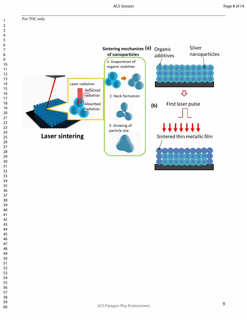
Fig 1 is the schematic depicting the process of printing, laser sintering and fabricating a strain sensor on commercially available bandage substrate. Silver nanoparticle ink is used to print the strain sensor design using aerosol jet printer. Faster processing speed and higher resolution can be achieved using the aerosol jet technique for printed electronic applications. The metal nanoparticles ink is generally stabilized by an organic layer to keep them well-dispersed in solution. For achieving conductivity on nanoparticles, the organic layer needs to be decomposed after printing. Thus a post-processing step like sintering is required to degrade the additives and surfactants, evaporate the solvent and coalesce the nanoparticles in ink for conductivity. During sintering a neck is formed between the particles, which is triggered by Ostwald ripening and is followed by surface-to-volume reduction 35, thus leading to agglomeration of particles, which forms a continuous percolating network. This gives rise to a homogeneous and continuous pathway for electrons to flow leading to electrical conduction. However, commercially available bandages and plasters are based on polymer materials and not compatible with the conventional heat sintering processes, which usually requires temperatures above 100 °C. Post-print thermal annealing can degrade and/or burn the substrate. Moreover, thermal sintering method is applied to the whole substrate, and is unable to selectively anneal the printed patterns. Fibre-based laser source is used to sinter the metal tracks. Optimization of laser power, energy and scanning speed are carried out to suit the substrate and thus provide right sintering conditions. Laser sintering provides the advantage of localized heating such that the heat absorbed by the base material is minimum. The measured surface roughness for the bandage substrate is approximately 2.66 µm. The contact angle of the silver ink
on the substrate is 53.52º. Surface roughness plays a key role in determining the contact mechanism between the ink droplet and the substrate. It has been found that higher surface roughness of the substrate leads to higher contact angle of the ink, which in turn leads to better adhesion [38].
A high intensity energy is impinged on the silver film during laser sintering. The high intensity energy thus delivered increases the temperature of the printed nanoparticles to the melting point of silver due to photothermal effect [39] as shown in fig 2. The increase in the temperature at the irradiated area causes solvent to evaporate, organic additives to decompose and leads to a continuous metallic film [40]. Since the heat energy supplied to the silver nanoparticles is for a short duration, only the top silver films is affected and the underlying substrate is not damaged. Decomposition of the organic additives in the printed silver can lead to swelling effect, a common phenomenon seen for light or laser sintered films. Most of the laser energy is first absorbed by the nanoparticles near the top surface, thus producing a metallic layer. On application of second and third pulse, heat transfer from the top film surface takes place to rest of the unsintered nanoparticles. Simultaneously vaporization is also induced inside the silver nanoparticle films, thus resulting in thermal decomposition of the organic additives. Internal gas is not readily exhausted once the metallic silver layer is formed, subsequently resulting in film swelling during the re-melting stage. The measured water contact angle of the commercial silver ink on glass and bandage is shown in fig S1.
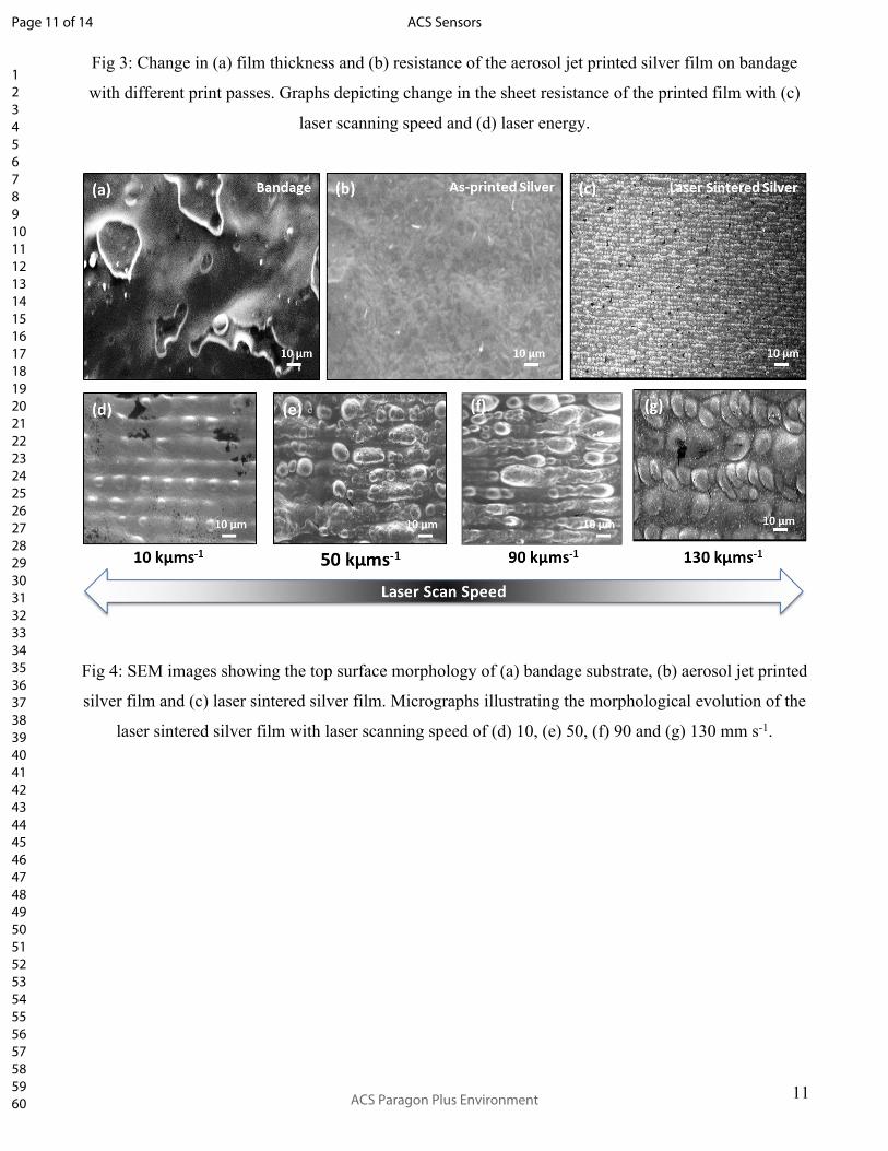
As explained above, the laser sintered thin films have marginally higher thickness compared to un-sintered films due to the swelling effect of the nanoparticles [40]. The thickness of the sintered film increases with increasing print passes from 0.46 µm, 0.65 µm, 0.93 µm, 1.19 µm for 4, 6, 8, 10 print passes respectively (fig 3a). A thin film may not be homogenous and thus lack connectivity between particles, an essential requirement for conductivity. A thick film, on the other hand, may lead to peeling under strain. Hence achieving optimal thickness is of paramount importance. Film thickness is expected to increase with print passes as more ink is deposited over the same area, which also explains decreasing resistance of the printed tracks (fig 3b). A high resistance is observed for the film with two print passes due to poor and non-uniform coverage. The sudden drop of resistance on printing four passes indicates minimum number of passes required to obtain a crack-free, uniform and electrically functional film.
The energy absorbed by the nanoparticles from the laser is dependent on many factors. We investigate the effect of laser energy density and scanning speed on the sheet resistance of printed strain sensor. Although same laser energy density could be achieved with different combination of laser parameters, the sintering time is significantly shorter for higher laser power and faster scanning speed. The laser power is fixed at 120 mW with a beam diameter of 60 µm, and the laser scan speed is varied from 10 to 150 mm s-1. Single-pass sintering is carried out in raster scan pattern. The sheet resistance of the printed samples sintered at various scan speeds is plotted in fig 3c. It can be observed that for all the samples, the sheet
resistance decreases as the laser scan speed reduces. The sheet resistance of the samples remains relatively constant for laser scan speed lower than 70 mm s-1. Laser sintering with a scan speed of 30 mm s-1 on six print passes results in the lowest sheet resistance. As observed the line thickness increases with the number of print passes. Thus a slower scan speed will be more effective for thicker printed line, as more energy will be absorbed resulting in better conductivity. Based on the observed trends, the laser scan speed process window can be categorised into two regimes namely, the incomplete and fully sintered regime. The threshold laser scan speed is found to be 90 mm s-1. The incomplete sintering regime is due to insufficient energy absorbed by the nanoparticles. This causes incomplete sintering, which in turn leads to poor neck formation and slow growth of particles. This results in incomplete sintering of the nanoparticles. At laser scan speed of 90 mm s-1 and below, the nanoparticles absorb sufficient energy to undergo neck formation and thus nanoparticles coalescence forming a continuous path. Figure 3d shows the effect of laser energy density on the sheet resistance. The laser energy density can be calculated from the laser power, beam diameter and the laser scan speed. Similar to the laser scan speed, the laser energy density also shows incomplete sintering regime and fully sintered regime with threshold laser energy density of about 20k J/m2. It is possible to tune the sheet resistance by changing the energy density of the laser.
SEM images are taken to investigate the morphology of the substrate and the printed films. As can be observed the bandage surface is uneven and riddled with pits (fig 4a). The surface contains many craters-like holes, thus leading to the high surface roughness. It is, thus, found that more than two print passes of conducting material are required to ensure continuous and smooth film on bandage. Fig 4b depicts the surface morphology of the as-printed silver film on the bandage with six print passes. The as-printing sample is evenly printed with no cracks or discontinuity. The effect of laser sintering can be seen in fig 4c, where nanoparticle coalesces and form a continuous film. However, laser causes small cracks and leaves a trail on the film. This observation suggests the possibility of the anisotropic electrical property of the laser sintered track, which requires further study (not in the scope of this paper). Laser sintering causes densification of the printed film, and the observed pores are caused by the decomposition of the silver precursors and volatilization of the organic matter in the ink. From SEM investigation it is apparent that the silver nanoparticle network is sufficiently sintered with dense grains. Suitable laser scanning speed is required to achieve sintering of nanoparticles, by allowing local temperature to reach suitable value. It is to be noted that no substrate damage is observed. Samples on glass are also prepared, which are heat treated (200 ºC for 2 h) and laser sintered (power 120 mW and scan speed 70 mm s-1) to compare with the bandage samples (supplementary information fig S2). The sheet resistance of the sintered film on glass for 2 and 6 print passes is 0.58 and 0.04 Ω/sq respectively. The laser sintered silver film on bandage has a sheet resistance of approximately 0.2 Ω/sq. SEM is engaged to investigate the effect of laser scan speed on the morphology of the printed films. Scanning the laser at 10 mm s-1 causes the
nanoparticles to agglomerate and form continuous track (fig 3d). However many cracks are visible on the entire substrate. Silver nanoparticle film sintered at scan speed of 50 and 90 mm s-1 have cracks and the printed tracks merge well to give more homogeneous coverage (fig 4e, f). Higher scan speed of 130 mm s-1 results in nanoparticles to swell (fig 4g).
When the laser beam interacts with silver nanoparticle ink, a photothermal effects takes places causing heat to be generated. The laser energy is absorbed by the silver nanoparticles, causing them to agglomerate. The large aggregates thus formed provide continuous tracks for electrical conduction. For the same laser power, a slower scan speed will give more time for the laser to interact with the silver nanoparticles, resulting in better sintering and lower overall resistance. For the given laser parameters, ink and bandage minimum 120 mW laser power is required for silver nanoparticles to conduct. A laser power of less than 120 mW leads to incomplete sintering process, thus resulting in high resistivity. A basic scotch tape test is also conducted to test the adherence of printed tracks on the bandage after laser sintering. The laser sintered film exhibits good adhesion and no peeling on removing the tape. Since laser sintering also produces localized heat, it is feared that the bandage could be damaged. The thermal stability of the bandage is analysed by TGA under normal atmosphere as shown in fig 5a. The thermal degradation curves of polyurethane show a single decomposition process. Approximately 91.5% of the polymer weight is lost either by evaporation or by degradation on heating up to 500 °C. The derivative curve shows that the degradation starts at approximately 225 °C and peaks at 395 °C. Although localized heating of the silver ink could exceed the degradation temperature of the bandage substrate, the polyurethane is able to withstand such localized heating. This is evident from the temperature profile, which decreases drastically at the silver-substrate interface to well below the degradation temperature. A tensile test is conducted to investigate the stretching ability of the polyurethane bandage substrate (fig 5b). A specimen with a dimension of 3 cm width and 10 cm length is used. The result showed that the substrate elongates almost linearly up to 27% strain. Besides, the polyurethane substrate had the remarkable stretching ability with an elongation at break of approximately 400%. The result indicated the suitability of the bandage for flexible electronics and home health devices.
FTIR analysis is carried out to ascertain that laser sintering is effective in removing organic additives to obtain pure metallic silver. Fig 5c shows the FTIR spectra for as-prepared (unsintered) and laser sintered films. The bands observed between 3000-2800 cm-1 in unsintered sample are attributed to symmetric and non-symmetric stretching of the hydroxyl and C-H bond with carbonyl. The characteristic bands of C=O and C-O occurring at 1680-1750 cm-1 and 1200-1350 cm-1 respectively indicate the presence of organic additives and surfactants in the printed silver ink. However, all the above peaks either reduce or disappear after laser sintering. The unsintered sample has a peak at a wavelength of 1400-1450 cm-1, which is the result of
uncertain residual organic binders and is also found to disappear after sintering.
Crystallinity and purity of silver before and after laser sintering is confirmed using XRD (fig 5d). The laser annealed silver film shows diffraction peaks at 64.6, 77.5 and 81.7, which can be indexed to (220), (311) and (222) planes of pure silver (JCPDS card 77-2100). The additional peaks at 44 and 98 can be assigned to scattering from the polyurethane substrate. Scherrer formula, shown below, can be used to deduce the crystallite size of the silver nanoparticles.
𝜏 = 0.94 𝜆β cos θ
λ is the wavelength of the incident X-ray (λ=0.154 nm for Cu K-alpha), β is the full width half maximum (FWHM) in radians and θ is the diffraction angle in radians. The calculated value of the crystallize size is approximately 32.5 nm. It can be seen that the estimated crystallite size using XRD is slightly larger than the nanoparticle size found in the ink. This can be attributed laser sintering, which may cause swelling and enlarging of the nanoparticles. There are two mechanisms responsible for size enlargement of nanoparticles- Ostwald ripening and oriented attachment. Both phenomena are dependent on temperature. Laser sintering raises the temperature in and around the nanoparticles. In the first case, the growth of the larger particles is due to the dissolution of the smaller ones and redeposition onto larger crystals or sol particles, while in the second phenomenon through merging the smaller ones. Ostwald ripening occurs because larger particles are more energetically stable than smaller particles. Temperature influences Ostwald ripening due to its effect on the interfacial energy, growth rate coefficients, and solubility. This is how the laser sintering drives the formation of bigger crystals.
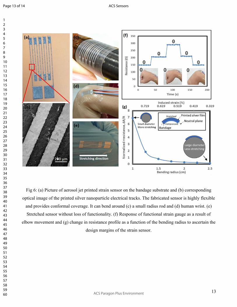
Fig 6a shows the fabricated strain sensor on the commercial bandage. Aerosol jet technology enables flexibility and high-resolution printing, thus allowing good printability. The high magnification optical image of the sensor reveals continuous printed lines without any cracks (fig 6b). The aerosol jet printed track has a line resolution of 200 µm. The fabricated sensor is intended to be used as wearable, hence flexibility is highly desired. As can be seen, the strain sensor could be rolled around a rod or applied to the wrist conformably (fig 6c,d). The printed sensor can be stretched and bended to a certain degree without losing functionality (fig 6e).
The strain gauge is attached to the wrist to be used on skin as home healthcare device to detect strain induced by human joint movements. As a proof-of-concept demonstration, the bandage is adhered conformably and tightly onto the surface of the human wrist. Since the bandage can be easily bent and stretched, it is able to sense the motion of the wrist. The strain gauge is printed with six print passes and laser sintered with a laser power of 120 mW and scan speed of 70 mm s-1. Fig 6f shows the response of functional strain gauge as a result of wrist movement. The printed strain gauge is able to give consistent and stable response for each wrist movement. When no strain is applied, the absolute resistance measured is 150 Ω. The resistance of the bandage increases to approximately 200 Ω when the strain is applied (wrist is bent approximately 45°).
On further bending the wrist, more strain is experienced by the bandage leading to the higher resistance value. As the wrist bends forward, the strain induced by the wrist movement is mainly along the direction of the back hand, which is transferred to the bandage and causes the resistance to vary. However, when the strain is released, the resistance of the bandage goes back to the original values. The bandage strain sensor successfully responds to the sensitive movements of the wrist.
It is necessary to test the strain sensing function under curvature state to evaluate its reliability in applications where surfaces are not flat. For this purpose, the bandage-based strain sensor is adhered conformably on to the outer surface of rods with different diameters. We then try to quantify the amount of resistance based on the bending radius. Sensitivity is defined as the difference in resistance between the initial and final values divided by the initial resistance: ΔR/R and is crucial for a sensor’s performance. Charting out the change in resistance profile as a function of the bending radius provide additional information to consider the design margins and working limit of the bandage-based strain sensor. As can be observed in fig 6g, the low bending radius of 1 cm induces a big change in resistance from the initial value due to the smaller curve of bending (higher strain). As the bending radius is increased, the bandage sensor experiences lesser strain, thus leading to smaller change in overall resistance. The region with large resistance change (up to 7) occurs for a relatively small bending radius change of 1.3 cm. Theoretically, the overall resistance of the sensor consists of the sum of local regions, and sensitivity of the sensor tends to be governed by region of high strain activity. The gauge factor (GF) measures the sensitivity of a strain sensor and is defined by:
GF= ΔR
L0ΔL
𝐿
where Ro is the original resistance, ΔR is the resistance change (ΔR= R-Ro), L0 is the initial length of the strain sensor and ΔL is the difference in the length of the sensor at the stretched condition and initial length, L.
Fig 7 shows the cyclic test result of the printed strain gauge, which is bent repeatedly at a radius of 5 mm for 700 cycles. It is to be noted that the resistance for the first 400 cycles increases gradually and then stabilizes and remains so for up to 700 cycles. Beyond 700 cycles the resistance starts to increase. Upon investigation under SEM some cracks are observed in the printed circuit (fig 7b). Although the resistance increases by about 10% (for 700 cycles), the strain gauge remains conductive and functional. Trend of resistance increasing in the early part of the cyclic test has been observed by other researchers.2, 36 The effect is attributed to voids and microcracks present in the film made of nanoparticles.37 These defects are found at the weaker points in the nanoparticle film, where the deformation exceeds the local elastic limit, thus causing permanent and irreversible damage. The electron transport is disrupted at these points, thus reducing the conductance of the thin film. We attribute the initial increase in the resistance to the breaking-in (mechanical run-in) of the silver nanoparticles film. Basically, it means that the nanoparticles in the film undergo a process of small shape and position adjustments due to the cyclical loading. There is
another possible explanation for increase in the resistance for laser-sintered nanoparticle film. As mentioned earlier, the sintered silver nanoparticle film has very thin structure, especially at the swollen points, thus making them vulnerable to stretching (fig 2c). The increases in the resistance for first 400 cycles could be due to the breaking of the thin structure of swollen nanoparticles. The resistance stabilizes after 400 cycles as most of the thin structures have been broken leaving behind are sufficiently strong track of nanoparticles to withstand the cyclic load. Besides, the average response time of the strain sensor is calculated to be around 492.16 ms with a standard deviation of 92.27 ms (fig S3). The result demonstrates the potential of printing electronics on commercial bandage substrates for wearable electronics and home health devices.
A strain simulation is performed to investigate the mechanical reliability and film integrity of the sensor design on the PU substrate. In the simulation, the PU substrate is pulled at both ends in the direction of the strain. The strain gauge is assumed to be always intact with the substrate as the adhesion of the silver film to the PU substrate is not simulated here. We have simulated the stress distribution of the silver film and the PU substrate at strain 100%, and 150%. The strain sensor has a gauge width of 9 mm and gauge length of 1cm with 10 gauge lines of 0.2 mm and a thickness of 1 µm. Based on the simulation result, the strain sensor experiences more deformation at 150% strain as the PU substrate deforms more the PU substrate when stretched at higher strain. However, it is observed that the stress distribution of strain sensor around the active gauge lines/sensing area remains relatively uniform regardless of the degree of strain. This means that each gauge line in the strain gauge can measure the strain and change its resistance by an equal amount for good strain measurement despite its large area and the soft substrate. It is noted that the average stress on the gauge lines are approximately 10 MPa, 20 MPa, and 30 MPa for elongation of 50%, 100%, and 150% respectively. These values are well below the maximum tensile strength of silver (140 MPa), which means that the strain sensor is functional when the substrate is stretched.
CONCLUSIONSIn summary, this work studies the use of printed silver
nanoparticle-based strain sensor as a wearable sensing system for home healthcare applications, where different sensors are integrated on to a single low-cost substrate. The concept of laser sintering of aerosol jet printed silver tracks is discussed by showing that fiber laser is capable of locally sintering the metal nanoparticles without damaging the underlying substrate. The fabricated sensor is flexible, lightweight and can detect large induced strains. This work is a step forward in showcasing direct write techniques and alternate sintering route to incorporate sensors into object and substrates that are not compatible with conventional post-processing techniques.
ASSOCIATED CONTENT Supporting Information. Supporting Information Available: The following files are available free of charge.
REFERENCES1. Yamada, T.; Hayamizu, Y.; Yamamoto, Y.; Yomogida, Y.; Izadi-Najafabadi, A.; Futaba, D. N.; Hata, K., A stretchable carbon nanotube strain sensor for human-motion detection. Nature nanotechnology 2011, 6 (5), 296-301.2. Lee, J.; Kim, S.; Lee, J.; Yang, D.; Park, B. C.; Ryu, S.; Park, I., A stretchable strain sensor based on a metal nanoparticle thin film for human motion detection. Nanoscale 2014, 6 (20), 11932-11939.3. Ryu, S.; Lee, P.; Chou, J. B.; Xu, R.; Zhao, R.; Hart, A. J.; Kim, S.-G., Extremely elastic wearable carbon nanotube fiber strain sensor for monitoring of human motion. ACS nano 2015, 9 (6), 5929-5936.4. Gibbs, P. T.; Asada, H., Wearable conductive fiber sensors for multi-axis human joint angle measurements. Journal of neuroengineering and rehabilitation 2005, 2 (1), 7. DOI: https://doi.org/10.1186/1743-0003-2-75. Amjadi, M.; Pichitpajongkit, A.; Lee, S.; Ryu, S.; Park, I., Highly stretchable and sensitive strain sensor based on silver nanowire–elastomer nanocomposite. ACS nano 2014, 8 (5), 5154-5163.6. Qin, Y.; Peng, Q.; Ding, Y.; Lin, Z.; Wang, C.; Li, Y.; Xu, F.; Li, J.; Yuan, Y.; He, X., Lightweight, superelastic, and mechanically flexible graphene/polyimide nanocomposite foam for strain sensor application. ACS nano 2015, 9 (9), 8933-8941.7. Ge, J.; Sun, L.; Zhang, F. R.; Zhang, Y.; Shi, L. A.; Zhao, H. Y.; Zhu, H. W.; Jiang, H. L.; Yu, S. H., A Stretchable Electronic Fabric Artificial Skin with Pressure‐, Lateral Strain‐, and Flexion‐Sensitive Properties. Advanced Materials 2016, 28 (4), 722-728.8. Chossat, J.-B.; Tao, Y.; Duchaine, V.; Park, Y.-L. In Wearable soft artificial skin for hand motion detection with embedded microfluidic strain sensing, Robotics and Automation (ICRA), 2015 IEEE International Conference on, IEEE: 2015; pp 2568-2573.9. Agarwala, S.; Goh, G. L.; Yap, Y. L.; Goh, G. D.; Yu, H.; Yeong, W. Y.; Tran, T., Development of Bendable
Strain Sensor with Embedded Microchannels using 3D Printing. Sensors and Actuators A: Physical 2017. DOI: https://doi.org/10.1016/j.sna.2017.07.02510. Comini, E., Metal oxide nanowire chemical sensors: Innovation and quality of life. Materials Today 2016, 19 (10), 559-567.11. Tan, H.; Tran, T.; Chua, C., A review of printed passive electronic components through fully additive manufacturing methods. Virtual and Physical Prototyping 2016, 11 (4), 271-288.12. Saengchairat, N.; Tran, T.; Chua, C.-K., A review: Additive manufacturing for active electronic components. Virtual and Physical Prototyping 2017, 12 (1), 31-46.13. Liu, Z.; Qi, D.; Guo, P.; Liu, Y.; Zhu, B.; Yang, H.; Liu, Y.; Li, B.; Zhang, C.; Yu, J., Thickness‐Gradient Films for High Gauge Factor Stretchable Strain Sensors. Advanced Materials 2015, 27 (40), 6230-6237.14. Wang, C.; Li, X.; Gao, E.; Jian, M.; Xia, K.; Wang, Q.; Xu, Z.; Ren, T.; Zhang, Y., Carbonized silk fabric for ultrastretchable, highly sensitive, and wearable strain sensors. Advanced materials 2016, 28 (31), 6640-6648.15. Kim, J.; Lee, M.; Shim, H. J.; Ghaffari, R.; Cho, H. R.; Son, D.; Jung, Y. H.; Soh, M.; Choi, C.; Jung, S., Stretchable silicon nanoribbon electronics for skin prosthesis. Nature communications 2014, 5, 5747. DOI: 10.1038/ncomms6747 16. Park, M.; Park, J.; Jeong, U., Design of conductive composite elastomers for stretchable electronics. Nano Today 2014, 9 (2), 244-260.17. Muth, J. T.; Vogt, D. M.; Truby, R. L.; Mengüç, Y.; Kolesky, D. B.; Wood, R. J.; Lewis, J. A., Embedded 3D printing of strain sensors within highly stretchable elastomers. Advanced Materials 2014, 26 (36), 6307-6312.18. Chen, S.; Wei, Y.; Yuan, X.; Lin, Y.; Liu, L., A highly stretchable strain sensor based on a graphene/silver nanoparticle synergic conductive network and a sandwich structure. Journal of Materials Chemistry C 2016, 4 (19), 4304-4311.19. Liao, X.; Liao, Q.; Zhang, Z.; Yan, X.; Liang, Q.; Wang, Q.; Li, M.; Zhang, Y., A Highly Stretchable ZnO@ Fiber‐Based Multifunctional Nanosensor for Strain/Temperature/UV Detection. Advanced Functional Materials 2016, 26 (18), 3074-3081.20. Allen, M. L.; Aronniemi, M.; Mattila, T.; Alastalo, A.; Ojanperä, K.; Suhonen, M.; Seppä, H., Electrical sintering of nanoparticle structures. Nanotechnology 2008, 19 (17), 175201. doi:10.1088/0957-4484/19/17/17520121. Perelaer, J.; Jani, R.; Grouchko, M.; Kamyshny, A.; Magdassi, S.; Schubert, U. S., Plasma and microwave flash sintering of a tailored silver nanoparticle ink, yielding 60% bulk conductivity on cost‐effective polymer foils. Advanced Materials 2012, 24 (29), 3993-3998.22. Hösel, M.; Krebs, F. C., Large-scale roll-to-roll photonic sintering of flexo printed silver nanoparticle electrodes. Journal of Materials Chemistry 2012, 22 (31), 15683-15688.23. Galagan, Y.; Coenen, E. W.; Abbel, R.; van Lammeren, T. J.; Sabik, S.; Barink, M.; Meinders, E. R.; Andriessen, R.; Blom, P. W., Photonic sintering of inkjet
printed current collecting grids for organic solar cell applications. Organic Electronics 2013, 14 (1), 38-46.24. Sarkar, S. K.; Gupta, H.; Gupta, D., Flash Light Sintering of Silver Nanoink for Inkjet-Printed Thin-Film Transistor on Flexible Substrate. IEEE Transactions on Nanotechnology 2017, 16 (3), 375-382.25. Joo, S.-J.; Hwang, H.-J.; Kim, H.-S., Highly conductive copper nano/microparticles ink via flash light sintering for printed electronics. Nanotechnology 2014, 25 (26), 265601. doi:10.1088/0957-4484/25/26/26560126. Liu, Y.-K.; Lee, M.-T., Laser direct synthesis and patterning of silver nano/microstructures on a polymer substrate. ACS applied materials & interfaces 2014, 6 (16), 14576-14582.27. Choi, J. H.; Ryu, K.; Park, K.; Moon, S.-J., Thermal conductivity estimation of inkjet-printed silver nanoparticle ink during continuous wave laser sintering. International Journal of Heat and Mass Transfer 2015, 85, 904-909.28. Peng, P.; Hu, A.; Zhou, Y., Laser sintering of silver nanoparticle thin films: microstructure and optical properties. Applied Physics A 2012, 108 (3), 685-691.29. Hong, S.; Yeo, J.; Kim, G.; Kim, D.; Lee, H.; Kwon, J.; Lee, H.; Lee, P.; Ko, S. H., Nonvacuum, maskless fabrication of a flexible metal grid transparent conductor by low-temperature selective laser sintering of nanoparticle ink. ACS nano 2013, 7 (6), 5024-5031.30. Das, S. R.; Nian, Q.; Cargill, A. A.; Hondred, J. A.; Ding, S.; Saei, M.; Cheng, G. J.; Claussen, J. C., 3D nanostructured inkjet printed graphene via UV-pulsed laser irradiation enables paper-based electronics and electrochemical devices. Nanoscale 2016, 8 (35), 15870-15879.31. Lin, Y.; Van Kerschaver, E.; Cabanas-Holmen, K. In Laser sintering of screen-printed silver paste for silicon
solar cells, Photovoltaic Specialists Conference (PVSC), 2013 IEEE 39th, IEEE: 2013; pp 3445-3447.32. Park, J. J.; Hyun, W. J.; Mun, S. C.; Park, Y. T.; Park, O. O., Highly stretchable and wearable graphene strain sensors with controllable sensitivity for human motion monitoring. ACS applied materials & interfaces 2015, 7 (11), 6317-6324.33. Suzuki, K.; Yataka, K.; Okumiya, Y.; Sakakibara, S.; Sako, K.; Mimura, H.; Inoue, Y., Rapid-response, widely stretchable sensor of aligned MWCNT/elastomer composites for human motion detection. ACS Sensors 2016, 1 (6), 817-825.34. Jeon, J.-Y.; Ha, T.-J., Waterproof electronic-bandage with tunable sensitivity for wearable strain sensors. ACS applied materials & interfaces 2016, 8 (4), 2866-2871.35. Perelaer, J.; Smith, P. J.; Mager, D.; Soltman, D.; Volkman, S. K.; Subramanian, V.; Korvink, J. G.; Schubert, U. S., Printed electronics: the challenges involved in printing devices, interconnects, and contacts based on inorganic materials. Journal of Materials Chemistry 2010, 20 (39), 8446-8453.36. Borghetti, M.; Serpelloni, M.; Sardini, E.; Pandini, S., Mechanical behavior of strain sensors based on PEDOT: PSS and silver nanoparticles inks deposited on polymer substrate by inkjet printing. Sensors and Actuators A: Physical 2016, 243, 71-80.37. Sangeetha, N. M.; Decorde, N.; Viallet, B.; Viau, G.; Ressier, L., Nanoparticle-based strain gauges fabricated by convective self assembly: Strain sensitivity and hysteresis with respect to nanoparticle sizes. The Journal of Physical Chemistry C 2013, 117 (4), 1935-1940.


![Wearable and Ultrasensitive Strain Sensor Based on High ...ms.fudan.edu.cn/fxs/download/2020/2020_13.pdf · wearable and real-time human motion-detecting devices, [15,16] and they](https://static.documents.pub/doc/80x56/5fe68459f360267ff666779c/wearable-and-ultrasensitive-strain-sensor-based-on-high-msfudaneducnfxsdownload2020202013pdf.jpg)
