50
Registration number 7 Weather Station Supervised by Dr Mark Fisher University of East Anglia Faculty of Science School of Computing Sciences

Registration number 7
Weather Station
Supervised by Dr Mark Fisher
University of East Anglia
Faculty of Science
School of Computing Sciences

Abstract
This paper describes the development of a weather station device. This device consists
of a temperature circuit and voltage-to-frequency converter which acts as a weather sta-
tion receiver. The measured temperature will then be displayed on the Altera board.
The objective of this paper is to explain and demonstrate how each of the components
in the device is used to measure the weather temperature. Once this device is developed,
it will be tested to make sure that the weather station is fully functional.
Acknowledgements
First and foremost, I would like to take this opportunity to express my deepest apprecia-
tion to all of the people that have been continuously giving me advices, encouragement
and support throughout the process of completing this Final Year Project. Without their
continuous support this project would not have been completed as it would be.
Throughout the whole process of this project, I have gained a lot of experience and
knowledge. I would like to express my deepest gratitude to Dr. Mark Fisher, my su-
pervisor, for his generous guidance and advices throughout this project. I am also very
thankful to Peter Trollope for his assistance in the Lewin lab.
Finally, I would like to express my greatest appreciation to Zul and my family and
friends for their advices, encouragement, patience and full support, throughout this pro-
cess of completing this project.
CMPC3P1Y Contents
Contents
1 Introduction 1
1.1 Aims and Objectives . . . . . . . . . . . . . . . . . . . . . . . . . . . 1
1.2 Motivation . . . . . . . . . . . . . . . . . . . . . . . . . . . . . . . . . 2
1.3 Risk and open issues . . . . . . . . . . . . . . . . . . . . . . . . . . . 2
1.4 Structure of the Report . . . . . . . . . . . . . . . . . . . . . . . . . . 3
2 Background and Literature Review 3
2.1 Semiconductor Temperature Sensor . . . . . . . . . . . . . . . . . . . 5
2.1.1 Thermocouple . . . . . . . . . . . . . . . . . . . . . . . . . . 5
2.1.2 Resistance Temperature Detectors(RTDs) and Thermistors . . . 5
2.1.3 2-Terminal IC Temperature Transducer . . . . . . . . . . . . . 5
2.1.4 Comparison of temperature sensor type . . . . . . . . . . . . . 6
2.1.5 2-Terminal IC Temperature Transducer - AD590 . . . . . . . . 6
2.2 Operational Amplifier . . . . . . . . . . . . . . . . . . . . . . . . . . . 8
2.2.1 Common Types of Applications . . . . . . . . . . . . . . . . . 9
2.2.2 Inverting Amplifier . . . . . . . . . . . . . . . . . . . . . . . . 9
2.3 Voltage to Frequency Counter . . . . . . . . . . . . . . . . . . . . . . 10
2.3.1 Astable Multivibrator . . . . . . . . . . . . . . . . . . . . . . . 11
2.3.2 Astable Operation Using 555 Timer . . . . . . . . . . . . . . . 11
2.3.3 How the astable circuit works . . . . . . . . . . . . . . . . . . 12
2.4 Application . . . . . . . . . . . . . . . . . . . . . . . . . . . . . . . . 13
2.4.1 Analog to Digital Conversion (ADC) . . . . . . . . . . . . . . 13
2.5 Altera MAX II Devices . . . . . . . . . . . . . . . . . . . . . . . . . . 14
2.5.1 Features . . . . . . . . . . . . . . . . . . . . . . . . . . . . . . 14
2.6 Philips PM 3055 Oscilloscope . . . . . . . . . . . . . . . . . . . . . . 15
2.7 Digitek DT-4000ZB . . . . . . . . . . . . . . . . . . . . . . . . . . . . 16
3 Methodology 16
3.1 Introducton . . . . . . . . . . . . . . . . . . . . . . . . . . . . . . . . 16
Reg: 7 iii

CMPC3P1Y Contents
3.2 Circuit design and requirements . . . . . . . . . . . . . . . . . . . . . 17
3.2.1 Temperature Circuit . . . . . . . . . . . . . . . . . . . . . . . 17
3.3 Frequency Converter . . . . . . . . . . . . . . . . . . . . . . . . . . . 19
3.4 AD590 . . . . . . . . . . . . . . . . . . . . . . . . . . . . . . . . . . . 20
3.5 Printed Circuit Board(PCB) Design . . . . . . . . . . . . . . . . . . . 21
3.5.1 PCB Mask Consideration . . . . . . . . . . . . . . . . . . . . . 21
3.6 PCB Masks . . . . . . . . . . . . . . . . . . . . . . . . . . . . . . . . 22
3.7 PCB Manufacture . . . . . . . . . . . . . . . . . . . . . . . . . . . . . 22
3.7.1 Inspection . . . . . . . . . . . . . . . . . . . . . . . . . . . . . 23
3.7.2 drilling . . . . . . . . . . . . . . . . . . . . . . . . . . . . . . 23
3.7.3 Soldering . . . . . . . . . . . . . . . . . . . . . . . . . . . . . 24
3.8 Weather Station Receiver . . . . . . . . . . . . . . . . . . . . . . . . . 25
3.9 Altera Board . . . . . . . . . . . . . . . . . . . . . . . . . . . . . . . . 26
3.10 ELT II Clock Configuration . . . . . . . . . . . . . . . . . . . . . . . . 27
3.11 Process . . . . . . . . . . . . . . . . . . . . . . . . . . . . . . . . . . 28
3.11.1 Design and Software Implementation . . . . . . . . . . . . . . 28
3.11.2 Clock Divider . . . . . . . . . . . . . . . . . . . . . . . . . . . 29
3.11.3 Counter . . . . . . . . . . . . . . . . . . . . . . . . . . . . . . 31
3.11.4 Decade Counter Timing Diagram . . . . . . . . . . . . . . . . 33
3.12 LED Display Driver . . . . . . . . . . . . . . . . . . . . . . . . . . . . 35
4 Testing 37
4.1 Receiver . . . . . . . . . . . . . . . . . . . . . . . . . . . . . . . . . . 37
4.1.1 Temperature Circuit . . . . . . . . . . . . . . . . . . . . . . . 37
4.1.2 Voltage-to-Frequency Converter . . . . . . . . . . . . . . . . . 37
4.2 Altera Board . . . . . . . . . . . . . . . . . . . . . . . . . . . . . . . . 38
4.3 Weather Station System . . . . . . . . . . . . . . . . . . . . . . . . . . 39
5 Conclusion 40
5.1 Evaluation . . . . . . . . . . . . . . . . . . . . . . . . . . . . . . . . . 41
5.1.1 Successes . . . . . . . . . . . . . . . . . . . . . . . . . . . . . 41
Reg: 7 iv

CMPC3P1Y Contents
5.2 Changes made and Further work . . . . . . . . . . . . . . . . . . . . . 42
5.2.1 Weather Station Receiver . . . . . . . . . . . . . . . . . . . . . 42
References 44
Reg: 7 v

CMPC3P1Y 1 Introduction
1 Introduction
A weather station is a device that can collect data from the weather using different kind
of sensors. The weather station in this project can be used as a personal or home weather
forecaster. A weather station can measure different type of weather elements. It can be
a thermometer, an anemometer, a barometer, a hygrometer and a rain gauge. A ther-
mometer takes the measurement of the temperature, anemometer for measuring wind
speed, barometer to measure the pressure, hygrometer for measuring humidity and rain
gauge to measure liquid. The device comes in many forms, both analogue and digital.
Nowadays, most devices are digital and they can be to the computer or internet. The
collected data can be analysed using weather station software.
The weather station has a receiver that will collect the weather data such as such as
high/low temperature, humidity and barometric pressure. These receiver will send the
collected data to an electronic device and will be displayed on the LED display.
In this project, the weather station system will measure only the temperature.
1.1 Aims and Objectives
The aim of this project is to develop a device that will measure the weather temperature,
using an Altera board. This project will report will explain and demonstrate how each
of the components in the device is used to measure the weather temperature. Once this
device is developed, it will be tested to make sure this system works fine.
The main objectives are:
• To design a temperature circuit.
• To design a voltage to frequency converter (Analog to Digital).
• Understand on how each design works.
• To understand on how the design logic components work in order to make the
LED of the Altera board work.
Reg: 7 1

CMPC3P1Y 1 Introduction
• To display the temperature value on Altera board.
• To produce a successful Weather Station System that can measure the tempera-
ture.
1.2 Motivation
Since Circuits And System module and Digital System Design (2013) modules will be
merged, new assignment need to be set up to enable the students to be exposed on the
aspects of both analogue and digital electronics. This project is quite interesting and
challenging as it requires a lot of understanding on how the systems works as well as
learn to solve any problem which may occur along the way. If this project is successful,
it will be an excellent idea to make it as one of the coursework and this system will be
used as a demonstration to the student.
1.3 Risk and open issues
There will a risks and issues while doing this project. This either can be cost, resource
and time.
When developing the hardware and software, it can be time consuming as there will
be possible risks, for example faulty components or delayed delivery of the compo-
nents. Faulty components can affect the system as it causes system failure. To mitigate
this risk, fully operational working receiver on the breadboard need to be produced and
additional components are needed for backup, in case any faulty occurs, so it can be
isolated and replaced immediately.
Testing software can take a lot of time due to bug fixes and time management is very
important so that there will be an ample time to fix other issues.
Completed device will be exposed to the weather changes, so waterproof casing is
needed to protect the device when the device is placed outside. The hardware compo-
nents and materials can be expensive. Therefore budget need to be set aside for this.
Reg: 7 2

CMPC3P1Y 2 Background and Literature Review
1.4 Structure of the Report
This report comprises of 5 main sections. Section 1 will briefly explain introduction,
aim and objectives, motivation as well as the risks and open issues that will possibly be
encountered during the process of completing in the project.
Section 2 presents the literature review, analyse the information from the articles,
journals, websites etc., that relates to the project design and theory that will be used in
the research. The information gathered can be used to explain the components of the
temperature circuit, the operation of the communication system for transmitting tem-
perature through a metal bar and the process of the Altera board that will display the
measured temperature.
The methodology and the procedures implemented in the project will be explained in
section 3. This includes the material, block diagram of overall project and procedure of
developing the device.
Section 4 presents the testing and result obtained from the designed system.
Lastly, section 5 concludes the overall project. Challenges encountered during the im-
plementation of the project will explained in this section. Recommendations for future
improvements will be provided in this section as well.
2 Background and Literature Review
Literature Review is very important in each project as it can serve as a foundation for
gathering information to complete the project. All information will be gathered from
various sources for instances books, journals, website and etc.
Once all of the information is gathered, it will be segregated according to its relevance
to this project. Previously, most students produce a simple and cheap weather station
that consists of a premade device such as Arduino or Raspberry PI. Once all of the in-
Reg: 7 3

CMPC3P1Y 2 Background and Literature Review
formation is gathered, it will be segregated according to its relevance to this project.
Previously, most students produce a simple and cheap weather station that consists of a
premade device such as Arduino or Raspberry PI.
An example, a user has developed a wireless outdoor Arduino weather station with
PC logging and Graphs. This device measure temperature, humidity and barometric
pressure. Since there are such devices in the market, the cost of the device was quite
high, so the user had developed this device, which is inexpensive and easy to build.
The components that have been used are: Arduino for remote sensors, XBee based
communication between the outdoor sensor and PC, Solar panel and Lipo battery for
outdoor sensor power, XBee Explorer connected to PC for communication reception
and C] based PC application to store, report and graph all of the data. Figure 2.1 shows
the Wireless outdoor Arduino weather station with PC logging and Graphs (Refer to
(zmashiah (2013)) the for more detailed information)
(a) The weather station device (b) The data log and the graph
Figure 2.1: Wireless outdoor Arduino weather station with PC logging and Graphs
In this project, the data will be displayed on the Altera board instead of being sent
to the computer. The main components that are used in this project are explained as
follow.
Reg: 7 4

CMPC3P1Y 2 Background and Literature Review
2.1 Semiconductor Temperature Sensor
Semiconductor Temperature Sensors form the fundamental of today’s electronic sen-
sors. The output of these devices is very linear and within a narrow range. There are
4 different types of temperature device that can be used to build a temperature circuit,
there are Thermocouples, Resistance Temperature Detectors and Thermistors and In-
tegrated Circuit temperature sensors. These sensors will convert the temperature into
current or resistance or voltage and this can be measured and compute the temperature.
2.1.1 Thermocouple
Thermocouple is an electrical device that responds to a difference in temperature by
producing a voltage. It consists of two metals joined together to form two junctions
which are hot and cold junctions. The hot junction is the sensor element and the cold
junction is kept at constant reference temperature (0C). (Haresh Khemani and Lamar
Stonecypher (2013))
2.1.2 Resistance Temperature Detectors(RTDs) and Thermistors
Resistance Temperature Detector is a temperature sensor used to measure temperature
by connecting the resistance of the metal changes with temperature. The function of
RTDs is as the sensing element is heated, the resistance of the metal wire increases pro-
portionally. (Innovative Sensor Technology (2013))
Meanwhile, Thermistors is like RTDs, vary their resistance as the temperature is
changed. The positive temperature coefficient (PTC) thermistors will show an increase
of resistance with increasing temperature, while negative temperature coefficient (NTC)
thermistors will show a decrease of resistance with increasing of temperature. (Omega
Engineering Inc (2013))
2.1.3 2-Terminal IC Temperature Transducer
Semiconductor temperature sensors are produced in the form of the integrated circuit.
The output will be a voltage or current proportional to absolute temperature. The output
Reg: 7 5

CMPC3P1Y 2 Background and Literature Review
is an excellent temperature within narrow range. (United Electric Controls (2013))
2.1.4 Comparison of temperature sensor type
The following figure 2.2 below shows the comparison of the different types of temper-
ature sensor.
Figure 2.2: Comparison of temperature sensor types
In conclusion, 2-Terminal IC Temperature Transducer is the best type of temperature
device to build the temperature circuit because of the linearity,stability and etc.
2.1.5 2-Terminal IC Temperature Transducer - AD590
Reg: 7 6

CMPC3P1Y 2 Background and Literature Review
(a) AD590 (b) AD590
Figure 2.3: AD590
AD590 is a 2-terminal integrated circuit temperature transducer. This temperature
transducer produces an output current proportional to absolute temperature current reg-
ulator ie. The output is equal to a scale factor multiplied by the temperature of the sensor
in degrees kelvin. This component can be used in any temperature-sensor application
which is below 150C.
Because of the high output impedance (>10 MΩ), the AD590 provide an excellent
elimination of supply voltage drift. For example, setting a power supply from 5V to
10V results in only 1C equivalent error or 1 mA maximum current change. Due to the
high impedance of the current output, the voltage drops over long lines can result the
insensitive of the device.
This transducer is durable because it withstands a voltage up to 44V and a negative
voltage of 20V. If the pin is in reverse or not enough power supply, the device won’t
damage.
The maximum deviation of current over temperature from best-fit straight line applied
to the non-linearity of the AD590. The non-linearity of the AD590 over the −55C to
150C range is greater to all conventional electrical temperature sensors. Figure 3.3
below shows the nonlinearity of AD590.
Reg: 7 7

CMPC3P1Y 2 Background and Literature Review
Figure 2.4: Nonlinearity
The specification of the AD590 as follow:
Absolute Maximum Ratings Forward Voltage +44 V
Reverse Voltage - 20V
Breakdown Voltage ±200V
Lead Temperature 300C
Voltage Range +4 to +30 Vdc Nominal Current Output at 25C
(298.2 K) 298.2 µA
Nominal Temperature Coefficient 1 µAK
Calibration Error J:±5C maximum K: ±2.5C
Calibration Adjustment J:±10.0C maximum (K: ±2.5C)
W/25C error set to zero J ±3.0C
Repeatability: ±0.1C maximum
Absolute Error ±0.1C/month max
More information can be found in AD590 Data sheet (2006).
2.2 Operational Amplifier
Operational Amplifier is an integrated circuit (IC) that worked as a voltage amplifier.
It is one of the most widely used component in the electronic circuits which produce a
Reg: 7 8

CMPC3P1Y 2 Background and Literature Review
small signal and it can increase the voltage or the power. (Floyd and Buchla (1995))
Figure 2.5: Symbol with dc supply connection
The op-amp requires two dc supply voltages which are positive and negative as shown
in figure 2.5. It has two input, the inverting input (-), the non-inverting input (+) and the
output terminal.
2.2.1 Common Types of Applications
The op-amp can be apply in many ways, this can be; inverting amplifier, non-inverting
amplifier, voltage follower operational amplifier. In this project, most of the design will
be using the inverting amplifier so knowing on how non-inverting amplifier works is
essential.
2.2.2 Inverting Amplifier
Reg: 7 9

CMPC3P1Y 2 Background and Literature Review
Figure 2.6: Inverting Amplifier
An operational amplifier connected as an inverting amplifier with amount of con-
trolled voltage gain is shown in figure 2.6. The input signal is applied through a series
input of resistor (Ri) to the inverting input(-) and the output is fed back through R f and
to the inverting input, while the non-inverting input(+) is connect to ground.
The output of the voltage can be compute as: V out = R fRi
2.3 Voltage to Frequency Counter
The voltage to frequency converter is an electronic circuit which convert the voltage
input into frequency output. The voltage input is integrate and converted into a ramp
signal which provides either positive voltage or negative voltage output, when the signal
is compared by the comparator. The output is going back to the integrator and produces
a triangular wave as the output. The integrator output compared by the comparator with
the zero reference and this will produce a square wave. (Young (1981))
Reg: 7 10

CMPC3P1Y 2 Background and Literature Review
2.3.1 Astable Multivibrator
It is also called as an astable multivibrator. An astable multivibrator is basically an os-
cillator which generates square-wave pulses that switch from high to low state and low
to high state continuously. The frequency of the pulses are determined by the resis-
tor/capacitor network that connects to the 555 timer externally.
2.3.2 Astable Operation Using 555 Timer
The 555 timer has three operating mode:
• Astable (oscillator)
• Bistable
• Monostable (one-shot)
One of simple and common used operating mode is the astable mode. Before know-
ing on how it works, it is necessary to know what each pin does.(Surtell (2013)) The
integrated circuit pin out is illustrated in Figure 2.7 below , the function of the pins will
explain below:
Figure 2.7: 555 Astable Circuit
Reg: 7 11

CMPC3P1Y 2 Background and Literature Review
• Pin 1 (Ground): Connects to the 0v power supply.
• Pin 2 (Trigger): The pin 2 control over pin 6, if the pin 2 and pin 6 is low, the
output will be high. If the pin 2 is low and pin 6 is high, the output will be low.
Basically when it detects 1/3 of supply voltage the output will be high.
• Pin 3 (Output): The output goes high during a constant period of time then it till
return to 0V.
• Pin 4 (Reset): Reset the operation.
• Pin 5 (Control): Allow the voltage to control the length of time of the Resis-
tor/Capacitor time constant, which can be used to vary the frequency and generate
the wave output. The higher the voltage, the periodic time will be longer and the
frequency will be low.
• Pin 6 (Threshold): If the pin 2 is high, it will detect the 2/3 of supply voltage and
the output will be low.
• Pin 7 (Discharge): The pin 7 is a discharge transistor and when the pin 6 has
tripped at the end of charging period for the external capacitor time constant, the
discharge transistor will cause the discharge period to commerce. The pin 3 will
be low until the capacitor discharged to 1/3 of supply voltage.
• Pin 8 (Supply): Connects to the positive power supply (+ve).
2.3.3 How the astable circuit works
To understand how the circuit works (figure 2.7 above); the pin 2 is connect directly to
pin 1. When the capacitor discharge, the timer is triggered and the voltage across the
capacitor will drop to 1/3 of supply voltage and the pin 2 will trigger the timer to start
another cycle. When the pin 3 is in a high condition, the discharge pin (pin 7) is open
which force the current through the resistor of R2 and C1. This cause the capacitor to
charge depends on the value of the resistors and capacitor.
Reg: 7 12
CMPC3P1Y 2 Background and Literature Review
The voltage at the pin 2 and pin 6 increases as the capacitor charge. When the volt-
age in pin 6 (threshold pin) reach the 2/3 of the supply voltage, the pin 3 will be low
output voltage. As the output at pin 3 low the discharge pin (pin 7) is connected to
ground which allow C1 to discharge. The value of the R2 and the value of the capac-
itor control the rate at which the capacitor discharges as the discharge occur through R2.
As the capacitor discharge, the voltage at pin 2 and 6 decreases and until the voltage
at trigger pin (pin 2) drops to 1/3 of the supply voltage cause the output at pin 3 to go
high. When the pin 3 goes high output, the discharge pin (pin 7) is opened and the cycle
will start over again. (Kleitz and Kleitz (1996)).
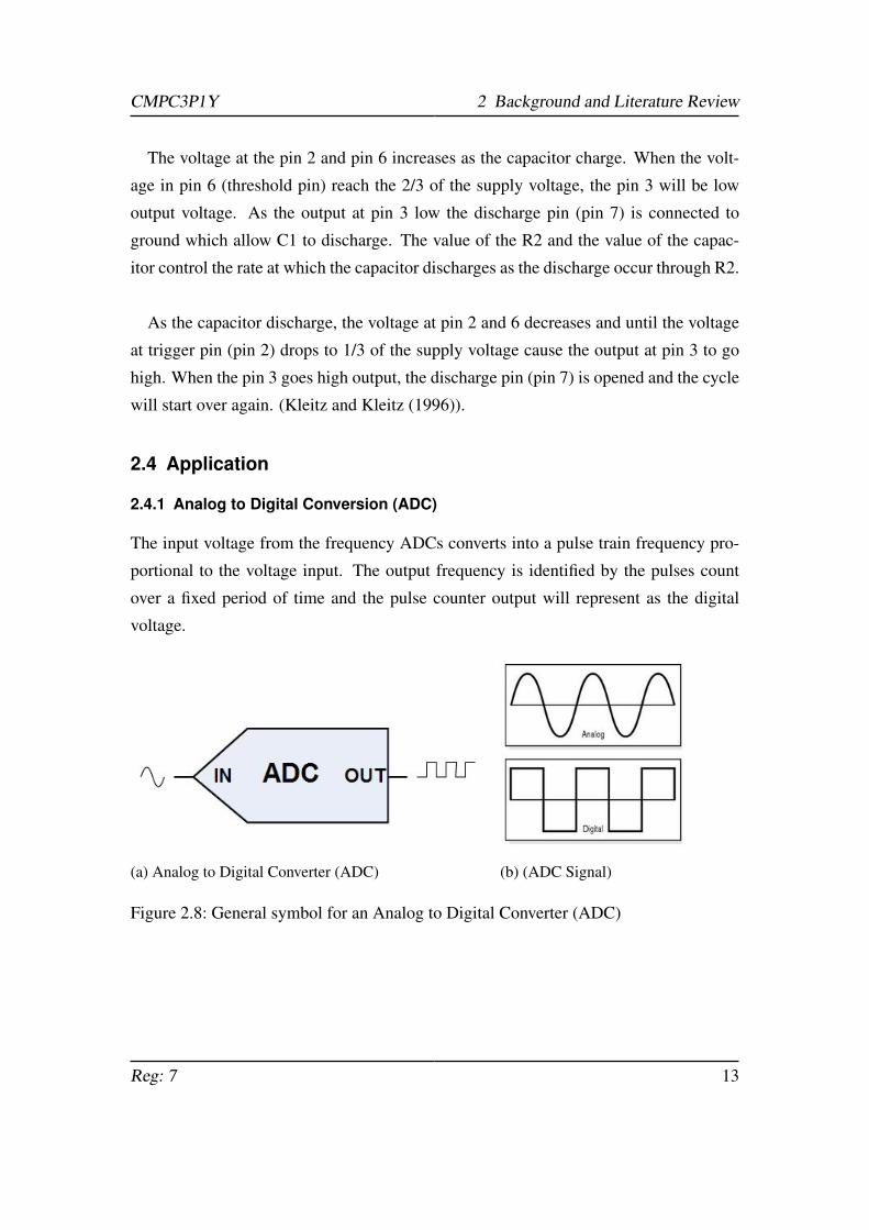
2.4 Application
2.4.1 Analog to Digital Conversion (ADC)
The input voltage from the frequency ADCs converts into a pulse train frequency pro-
portional to the voltage input. The output frequency is identified by the pulses count
over a fixed period of time and the pulse counter output will represent as the digital
voltage.
(a) Analog to Digital Converter (ADC) (b) (ADC Signal)
Figure 2.8: General symbol for an Analog to Digital Converter (ADC)
Reg: 7 13
CMPC3P1Y 2 Background and Literature Review
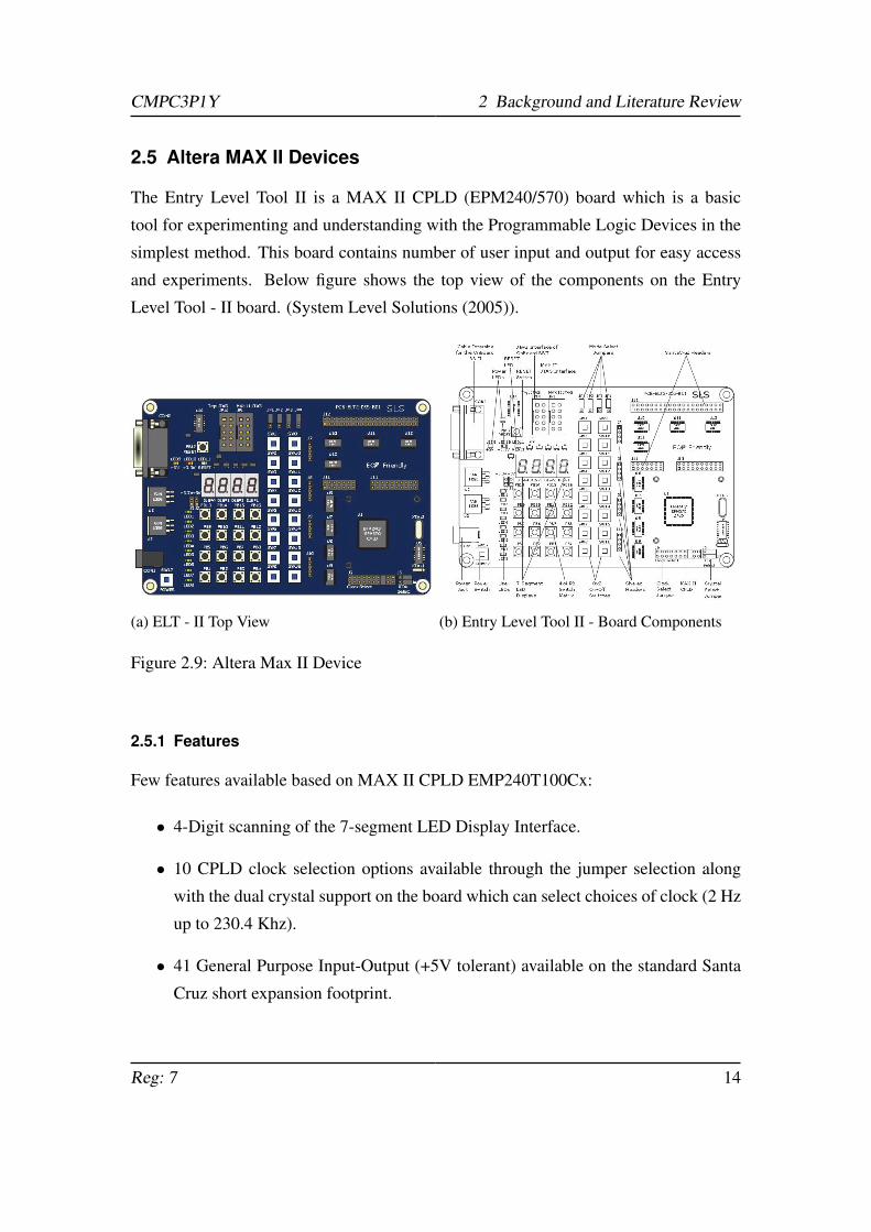
2.5 Altera MAX II Devices
The Entry Level Tool II is a MAX II CPLD (EPM240/570) board which is a basic
tool for experimenting and understanding with the Programmable Logic Devices in the
simplest method. This board contains number of user input and output for easy access
and experiments. Below figure shows the top view of the components on the Entry
Level Tool - II board. (System Level Solutions (2005)).
(a) ELT - II Top View (b) Entry Level Tool II - Board Components
Figure 2.9: Altera Max II Device
2.5.1 Features
Few features available based on MAX II CPLD EMP240T100Cx:
• 4-Digit scanning of the 7-segment LED Display Interface.
• 10 CPLD clock selection options available through the jumper selection along
with the dual crystal support on the board which can select choices of clock (2 Hz
up to 230.4 Khz).
• 41 General Purpose Input-Output (+5V tolerant) available on the standard Santa
Cruz short expansion footprint.
Reg: 7 14

CMPC3P1Y 2 Background and Literature Review
• Quartus II software Compatible for the on board logic for MAX II configuration
• On Board Power Supply for the smooth operation of the board
More features can be found at System Level Solutions (2005).
2.6 Philips PM 3055 Oscilloscope
Figure 2.10: Philip PM3055 Oscilloscope
An Oscilloscope is a device that display a graph of an electrical signal. The electric
signals can be a voltage, frequency or time. The graph will show a vertical (Y) axis
which is voltage and horizontal (X) axis will represent time. (Tektronix (2000)) There
are few features of using this oscilloscope:
• It can determine the signal of the voltage and time.
• Calculate the frequency of an oscillating signal.
• Able to find out how much of the signal is alternating current (AC) or direct
current (DC).
• If the signal is distorting, it shows that some part of the components are malfunc-
tion.
• Able to find out if the signal has produce a noise.
This device will be used as part of testing to make sure the system is working for this
project.
Reg: 7 15

CMPC3P1Y 3 Methodology
2.7 Digitek DT-4000ZB
A multimeter is an electronic measuring device to measure voltage, resistance, current,
temperature and frequency. This device can change from AC to DC. This device has an
LCD display screen that will display the value on the screen.
Figure 2.11: Digitek DT-4000ZB
This device will be used as part of testing to make sure the system is working for this
project.
3 Methodology
3.1 Introducton
Having completed the research essential for the project, it is necessary to decide how
the system would operate. Figure 3.1 below shows an overall picture of the weather
station.
Reg: 7 16

CMPC3P1Y 3 Methodology
Figure 3.1: Block diagram of overall Weather Station
The temperature circuit acts as the receiver of the weather station system. It col-
lects the temperature and converts it into a voltage. The output voltage which is an
analog signal is converted into a digital signal in the form of frequency at the Voltage-
to-Frequency Converter.
The frequency signal will then send to the Altera board to display the value on the
LED screen display.
3.2 Circuit design and requirements
3.2.1 Temperature Circuit
Few components are needed to develop the temperature circuit. Below are:
Table 3.1: Component list for the circuit
Description Notes
AD590 Temperature Transducer
AD581 Voltage Regulator
1KΩ,27KΩ,33KΩ,100KΩ Resistor
2.2KΩ,4.7KΩ,10KΩ Variable Resistor
4.7nF, 30pF Capacitor
OP177 0p-amp Ultraprecision Operational Amplifier
TL071 0p-amp Input Operational Amplifier
Reg: 7 17

CMPC3P1Y 3 Methodology
Figure 3.2: Circuit Design Overview
Figure 3.2 shows a temperature circuit taken from the AD590 Data sheet (2006) but
there are few additional components that have been added to the circuit in order to
achieve the requirements. In order to make this circuit working, AD590, the temperature
transducer need to be calibrated.
Figure 3.3: AD581 functional block diagram
The AD581 is a 3-pin, voltage reference which provides output of 10V (Analog De-
vices (2009)). The AD581 provide a full performance with an unregulated input range
from 12V to 30V.
Non-linearity is the major contributor to error over temperature in the circuit (temper-
ature circuit). The circuit can be trimmed by adjusting the variable resistor of the R1,
when the output is 0V and the sensor (AD590) is at 0C. The variable resistor of R2 is
Reg: 7 18

CMPC3P1Y 3 Methodology
then adjusted when the output is 10V output with the sensor (AD590) at 100C.
Ice water and boiling water is used to calibrate with the temperature for this circuit.
The output V+ of the operational amplifier must be greater than 17V and V− should be
at least -4V. There will be no voltage applied across the device, if −V is grounded. The
output of the temperature circuit will be between 0V to 10V.
The output of the temperature will then goes to the inverting operational amplifier
and the positive output will be converted into negative output. The inverting ampli-
fier in the circuit design above shows that the gain is up to 10, although only gain of 1
is needed to drive the output from the temperature to the voltage-to-frequency converter.
Below shows the calculation of the gain:
R1,R2 = 1KΩ
Rf = Variable Resistor (0-10KΩ)
3.3 Frequency Converter
Figure 3.4: Close look on Voltage-To-Frequency converter
Reg: 7 19

CMPC3P1Y 3 Methodology
The frequency converter circuit in design (refer to figure above 3.4) contains a TL071
op-amp which is an inverting integrator along with an NE555 timer (Dioszegi and Nagy
(2008)). The input voltage is range from 0V to -10V, and it will then produced an out-
put frequency of between 0 to 1000HZ. The current of C1 is the function of the input
voltage which is: Ic =−Vin
P1+R1
As the voltage on C1 reaches 23 of the Vcc, the NE555 timer internal discharge tran-
sistor will close and the voltage on C1 will return to 13 of the voltage of the Vcc, the
threshold. At 13 of the voltage, the discharge transistor will switch off, and C1 will start
to charge again. The NE555 output is high while C1 is charging and while C1 is dis-
charging, the output will be low. The following equation results for the output frequency
will be the product of the input voltage and the charging time: f out = VinP1+R1 .C1.
13Vcc.
P1 calibrates the relationship between the output of frequency and the input of the
voltage relationship calibrates by the P1. The accuracy of the voltage to the frequency
conversion decreases as the frequency decreases because of the discharge interval is ap-
proximately 30µsec. The error of the conversion range will be from 0.3 to 3% if the
frequency is assign to 100Hz as -1V and 1000Hz as -10V, The conversion will be less
than 1.3% over the whole range, if the output of the frequency is assigned to the middle
of the input voltage range at -5V and calibrate by the P1.
C1 should have low dissipation factor in order to improve the performance. P1 is a
multiturn, ceramic-metal potentiometer and if R1 has a low temperature coefficient, the
temperature dependence can be reduced.
3.4 AD590
The AD590 component is connected to a tube and linked to the BNC (Bayonet NeillConcelman)
connector on the temperature circuit in order to measure the temperature. By doing this,
it is more flexible and easier to move the components around. It would also be easier
to dip it into the ice water and boiling during calliboration. Figure 3.5 shows the AD50
component.
Reg: 7 20

CMPC3P1Y 3 Methodology
(a) AD590 Top View (b) AD590 Close View
Figure 3.5: AD590
3.5 Printed Circuit Board(PCB) Design
PCB can be manufactured, once the receiver is working. There are few procedures to
follow in order to produce an excellent quality of the board. A software namd "Eagle"
is used to design the PCB board:
• Use minimum jumper as possible to make sure the circuit is easy to trace.
• Ensure adequate spacing between components.
• Keep as much copper on the board as possible for shielding and useful for debug-
ging.
• If it is possible, keep the track in parallel so it is easy to detect the error.
• keep a copy of the previus version as a backup.
The most important when design the PCB is to keep as much copper on the board
function as a shield and it is very useful to make a modification, if there is a mistake. It
is recommended to label the components position on the board, although it will be time
consuming but it will be useful to identify the components.
3.5.1 PCB Mask Consideration
It is important to make sure the track and the layout of the circuit is correct, before
producing the PCB. Start with the circuit diagram and compare it with the track on
Reg: 7 21

CMPC3P1Y 3 Methodology
design then scribble out each of the line on the circuit design and corresponding track
on the PCB design. In the end there should not be any track left to scribble. Double
check to make sure that everything goes well. Lastly ensure the pin layouts of the
Integrated Circuit are checked according to the circuit design and the datasheet.
3.6 PCB Masks
It is useful to ink the tracks on the opposite of the sheet with the mask printed on to
an acetate sheet to ensure the UV light will not penetrate through the mask. The PCB
tracks will not etch correctly if the UV penetrate through the mask.
Figure 3.6: Temperature and Frequency Converter PCB Mask
3.7 PCB Manufacture
When the PCB had been manufactured, next stage is to install the components to the
board, this will require to first inspecting the board making sure the board is fine. Drill
the PCB to make a holes for the components to be installed and then solder it to make
sure the components stay on the board.
Reg: 7 22

CMPC3P1Y 3 Methodology
3.7.1 Inspection
During the inspection, there is no problem indicated with the PCB board.
3.7.2 drilling
The PCB will expose in a UV light box and then it will go through an etching process
to leave the copper tracks on the board. After the process, the board will need to be
drilled for the components to be soldered. Google need to be use while drilling for eye
protection.
Initially, the smallest drill need to be used first to make sure there is enough copper
left on the pad and making sure the components legs e.g. BNC, power blocks, etc. will
fit tight on the board. It will be easy to solder as the components held in place. For
the components with the large diameter legs, the drill size needs to be increased. The
smallest drill will be 0.5mm, medium drill is 0.8mm and the largest will be 1.5mm.
Figure 3.7: Micro Drill used for PCB drilling
Reg: 7 23

CMPC3P1Y 3 Methodology
3.7.3 Soldering
The components are needed to place through the holes of the board, so make sure the
components is flushed to the board and in the correct orientation. Once the components
are in the place, apply the solder to the one side of the joint. Make sure that the tip is
touching the component lead and the pad. Heat the legs and the pad before introducing
the solder to ensure that the solder runs neatly into the joint to leave a nice conical shape.
Ensure the board is clean and if oxidation detect on the board, use some wire wool and
gently clean it.
Figure 3.8: Comparing a good solder joint and dry solder joint(Asque (2012))
It is necessary to test all the solder joint with the shielding when all of the components
soldered in places so there will be no shorts occur. Good quality solder is useful as the
flux will remove any oxidants on the components leg or the pad. On completion make
sure that there is no dry joint and solder has not flowed incorrectly into any other path.
(Refer to figure 3.9 below)
A thin coat PCB protective lacquer will be applied to the trackside of the board once
all the joint has been tested. The function of the lacquer is to protect the tracks of the
PCB and ensure that the board are not exposed to oxidise.
Reg: 7 24
CMPC3P1Y 3 Methodology
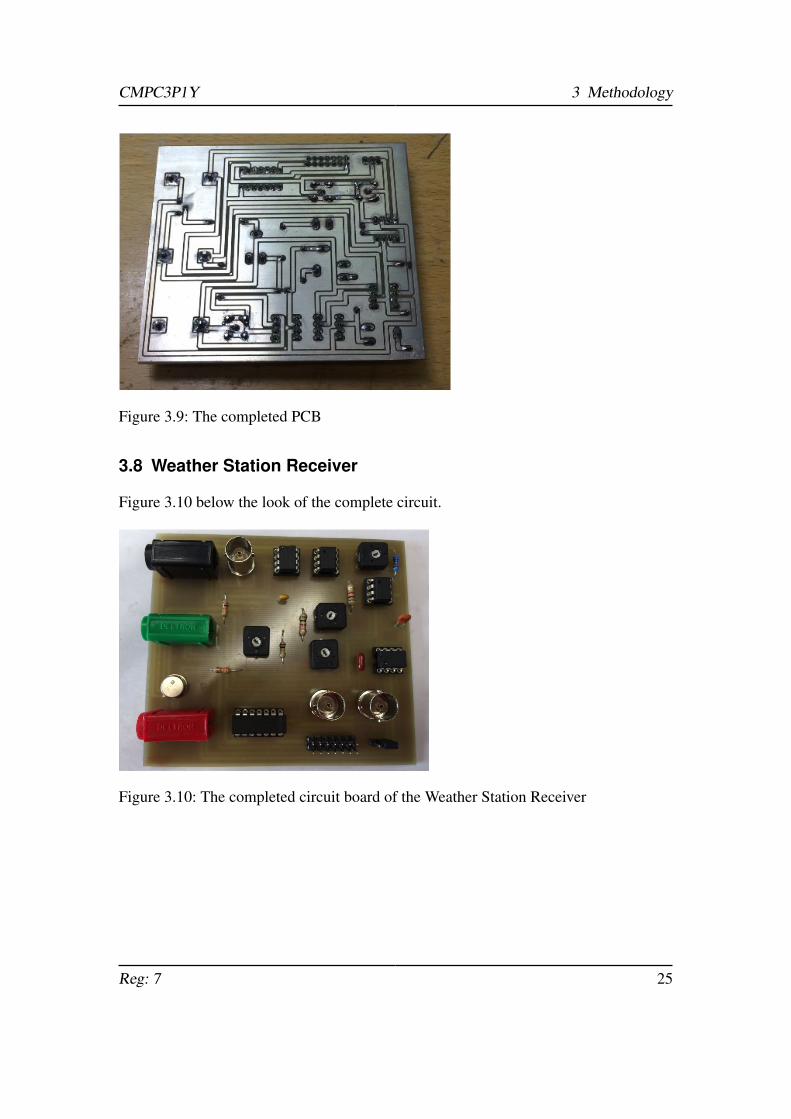
Figure 3.9: The completed PCB
3.8 Weather Station Receiver
Figure 3.10 below the look of the complete circuit.
Figure 3.10: The completed circuit board of the Weather Station Receiver
Reg: 7 25

CMPC3P1Y 3 Methodology
3.9 Altera Board
The signal of the weather station receiver will connect to the Altera board to display the
measured temperature. In order to achieve this, an 74LS14 chip (6 off inverter Gates,
Schmitt triggered)is used. (Texas Instruments (2002))
Figure 3.11: 74SL14
Only pin 7,8,9 and 14 of the chip is used for this. The pin 7 will connect to the ground,
pin 8 and 14 is connect to the female header, pin 9 is the input from the output of the
receiver. This chip act as a buffer in order to protect the Altera board from blown up.
The integrated circuit is connected to a female header where a piece of ribbon cable
will be used to connect to a J11 Expansion Prototype Connector on the Altera board. A
software called "Quartus" will be used to design the program for the board in order to
display the measured temperature.
Figure 3.12 below shows the overall circuit that connects to the Altera board.
Figure 3.12: Receiver connects to the Altera board
Reg: 7 26
CMPC3P1Y 3 Methodology
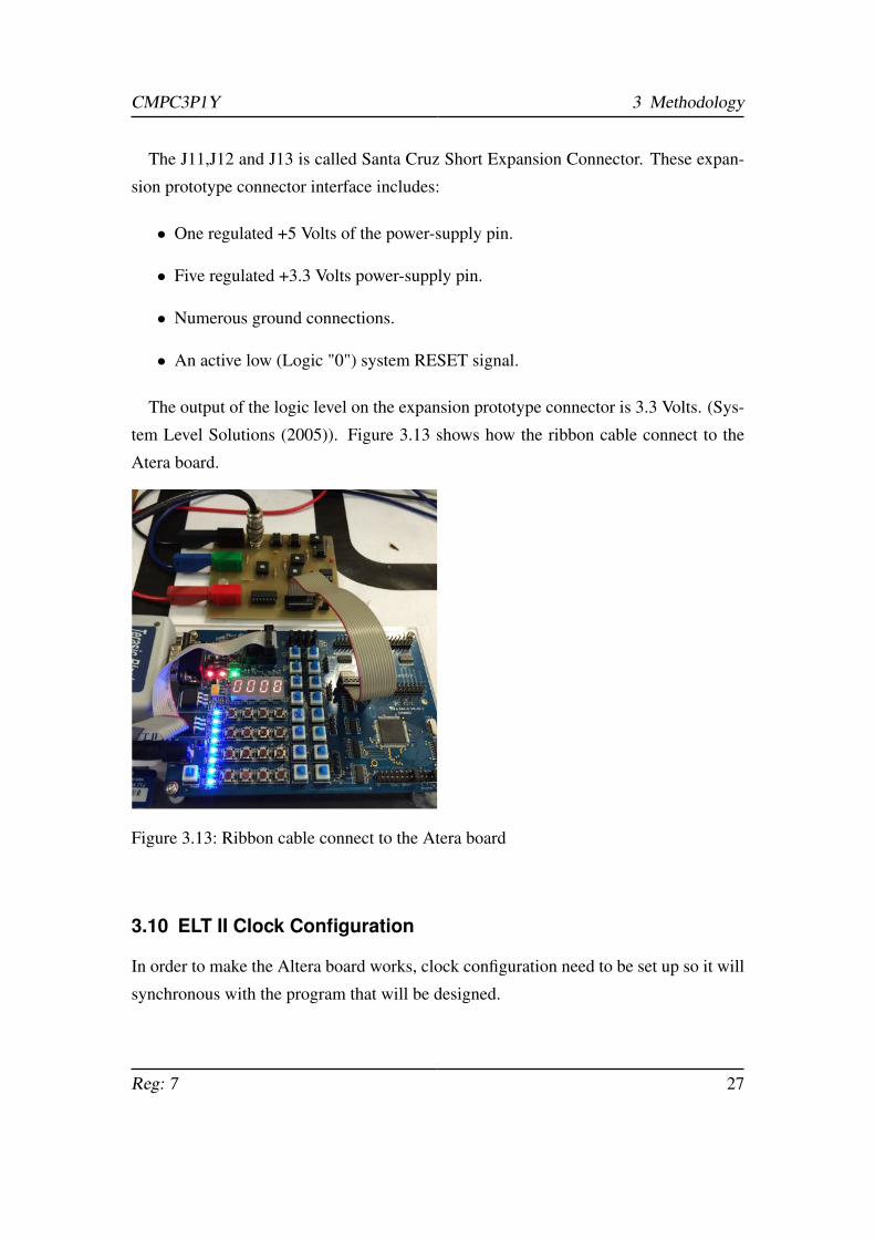
The J11,J12 and J13 is called Santa Cruz Short Expansion Connector. These expan-
sion prototype connector interface includes:
• One regulated +5 Volts of the power-supply pin.
• Five regulated +3.3 Volts power-supply pin.
• Numerous ground connections.
• An active low (Logic "0") system RESET signal.
The output of the logic level on the expansion prototype connector is 3.3 Volts. (Sys-
tem Level Solutions (2005)). Figure 3.13 shows how the ribbon cable connect to the
Atera board.
Figure 3.13: Ribbon cable connect to the Atera board
3.10 ELT II Clock Configuration
In order to make the Altera board works, clock configuration need to be set up so it will
synchronous with the program that will be designed.
Reg: 7 27

CMPC3P1Y 3 Methodology
Figure 3.14: ELT II Clock Configuration (System Level Solutions (2005))
In this board there are two crystals for the clock generator. 32.768 KHz will be
selected by making use of the jumper J4 and J5. The jumper setting for this selection
is Short J4.2-J4.1 and Short J5.2-J5.1. This selected crystal is connected to the 14-stage
Binary Counter and divider circuit. It generates a 10 Clock outputs and from the clock
ouputs, 512Hz (Short J6.5 and J6.6) has been selected.
3.11 Process
The board will display the measured temperature by taking the signal pulses from the
receiver and measure the period of the pulses. The period of the pulses are measured
depends on the temperature. Using the frequency counter, it will count the pulses and
display the result between 0-999 on the LED display of the board for a few seconds and
then it resets to 0 and counts again.
Few components need to be designed in order to achieve this:
• Clock divider.
• Frequency Counter.
• LED display driver.
3.11.1 Design and Software Implementation
Figure 3.15 below shows the overall design of the Altera board.
Reg: 7 28

CMPC3P1Y 3 Methodology
Figure 3.15: Overall design of the Altera Board
Each of the logic block in the diagram has it own fuctions: in this case there are the
clock divider, frequency counter and the LED display driver.
3.11.2 Clock Divider
A clock divider is also called a frequency divider. It provides an output signal that di-
vided the input of the frequency. There are different kinds of flip-flop to create the clock
divider: D flip-flop, T flip-flop, RS and JK flip-flop. T flip-flop is used for this project.
A T flip-flop is an edge driven device which toggles or swaps the state, on each of
the clock edge, which resulting half of the frequency of the signal to the input of the T
flip-flop.
Figure 3.16: Symbol for a T flip-flop
Reg: 7 29

CMPC3P1Y 3 Methodology
The characteristic equation, characteristic and Excitation table will described below:
Qnext −T ⊕Q = T Q+ T Q
T Q Qnext Comment
0 0 0 Hold State
0 1 1 Hold State
1 0 1 Toggle
1 1 0 Toggle
Q Qnext T
0 0 0
0 1 1
1 0 1
1 1 0
The right side of the table shows the Excitation table and the left side of the table
shows the characteristic table of the T flip-flop.
When 0 input goes to the T flip-flop, the next state will be the same like the present
state (example T = 0, present state = 0, therefore the next state will be 0). When 1 in-
put goes to the T flip-flop, the next state to the inverse of the present state will change
(example, when T = 1, the present state will be 0 and the next state will be 1). (Miller
(1939))
Figure 3.17 below shows the clock divider that will be used to design the program.
Figure 3.17: Clock Divider
Reg: 7 30

CMPC3P1Y 3 Methodology
512Hz clock has been chosen for the Altera board as an input and there are 8 T flip-
flop for the clock divider design. Using the T flip-flop, when the T is high, the T flip-flop
will divide the clock frequency by two; since the clock frequency is 512Hz, the output
frequency obtained from the T flip-flop will be 2 Hz.
3.11.3 Counter
Figure 3.18: SN74162
A counter is a device that displays the number of times when a clock signal has oc-
curred. A 4-bit decade counter (74162) is used for this design and these counter advance
one count with each positive clock transition, progressing from 0000 to 1001 and back
to 0000 in binary. The counter is a synchronous counter where the outputs change ac-
curately on each clock pulse. It counts from 0 to 9 (0000 to 1001 in binary).(Leach and
Malvino (1994))
The count enable(ENP), pre-set(LOAD), reset(CLR) and carry-in(ENT) input will be
high (1) and when the count enable is low(0) the clock input will be ignored and the
counter will stop counts. The counter can be pre-set by placing any binary number on
the input of the A to D, this can make the pre-set input to be low and a positive pulse
to the clock input. The input of the A to D can be remaining unconnected if it does not
require. The reset input will be active-low and when it is counting it will become high
(+Vs). When the reset is low (0), the counter will become 0 (0000 and the QA to QD
will become low as well). Since this counter is synchronous reset, the reset will occur
on the rising-edge of the clock input. (Hewes, John (2014))
Reg: 7 31

CMPC3P1Y 3 Methodology
Table 3.2 below shows the decade truth table.
Table 3.2: Decade Counter Truth Table
Clock count QD QC QB QA Decimal Value
1 0 0 0 0 0
2 0 0 0 1 1
3 0 0 1 0 2
4 0 0 1 1 3
5 0 1 0 0 4
6 0 1 0 1 5
7 0 1 1 0 6
8 0 1 1 1 7
9 1 0 0 0 8
10 1 0 0 1 9
Since the 74162 counter will liked together, the clock inputs will connect together,
the carry out(RCO) will feed into the carry in(ENT) of the next counter. The carry in
(ENT) of the first counter need to be high in order to make counter works. Figure 3.19
shows the example on how to connect the counter in chain and this can be applied to the
design. Figure 3.20 below shows the design of the counter.
Figure 3.19: Connecting synchronous counters in a chain (Miller (1939))
Reg: 7 32

CMPC3P1Y 3 Methodology
Figure 3.20: 74162 Counter connecting together in a chain
In this project, only 3 digits will be displayed on the board. The number is between
0-999 so only three of the 74162 counters are required for this design and figure 3.20
shows that cascading the counters allow it to count from 0-999 and making sure that the
carry out of the first counter is connecting to the carry in (enable) of the second counter.
The same is applied to the second counter where the carry out (RCO) is connected to
the carry in (enable) of the third counter. The ouput of the counter is used to drive the
display.
3.11.4 Decade Counter Timing Diagram
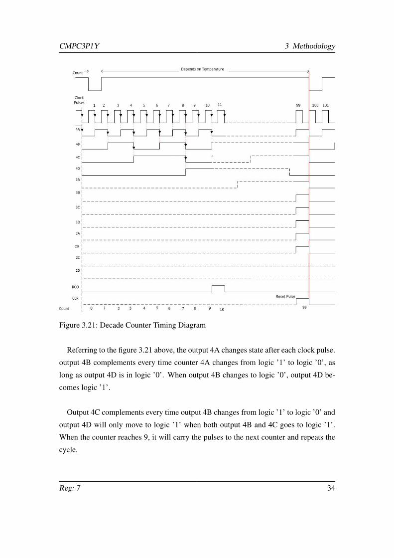
Figure 3.21 shows how the counter process works.
Reg: 7 33
CMPC3P1Y 3 Methodology
Figure 3.21: Decade Counter Timing Diagram
Referring to the figure 3.21 above, the output 4A changes state after each clock pulse.
output 4B complements every time counter 4A changes from logic ’1’ to logic ’0’, as
long as output 4D is in logic ’0’. When output 4B changes to logic ’0’, output 4D be-
comes logic ’1’.
Output 4C complements every time output 4B changes from logic ’1’ to logic ’0’ and
output 4D will only move to logic ’1’ when both output 4B and 4C goes to logic ’1’.
When the counter reaches 9, it will carry the pulses to the next counter and repeats the
cycle.
Reg: 7 34

CMPC3P1Y 3 Methodology
The 4C complements every time 4B goes from logic ’1’ to logic ’0’ and 4D remains
at logic ’0’ as long as 4B or 4C is logic ’0’. When the count reach to 9, it will carry
it the next counter and repeat. Figure 3.21 above, although the counter can reach up to
999, in this project the counter was configure in such a way it will set to ’reset’ when it
reaches 99.
In figure 3.21 above, although the counter can reach up to 99, in this project the
counter was configure in such a way it will set to ’reset’ when it reaches 999.
3.12 LED Display Driver
An output driver will be a circuit to run an output such as the LED display driven by the
counter. This driver is provided by Dr. Mark Fisher so that the LED display will run
smoothly.
(a) 74139(Texas Instruments
(1972))
(b) 74173(Texas Instru-
ments (1976))
(c) 7447 (Texas Instruments
(1974))
Figure 3.22: 74139, 74173 and 7447 chips
The driver consists of a Dual 2-Line to 4-Line Decoders/Demultiplexers (74139),
Registers(74173) and BCD to 7 Segments (7447). The demultiplexer is a circuit that
has more than one input and it is used to send a signal to one or many devices.
Reg: 7 35

CMPC3P1Y 3 Methodology
The registers are a group of flip-flops which is capable of storing one bit of informa-
tion and BCD to 7 Segments is used to drive the 7 segment display.
Figure 3.23: LED Display Driver)
Figure 3.23 shows how the LED display driver. The signal from the counter is sent
to the demultiplexer and the signal then goes to the 4 of the registers. The informaton
is stored in the registers and at the same time it will send the signal to the BCD to 7
Segments to display the value.
Reg: 7 36
CMPC3P1Y 4 Testing
4 Testing
4.1 Receiver
4.1.1 Temperature Circuit
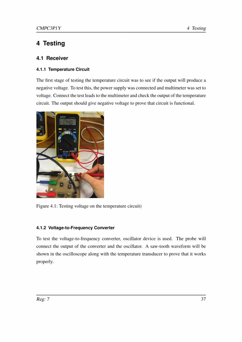
The first stage of testing the temperature circuit was to see if the output will produce a
negative voltage. To test this, the power supply was connected and multimeter was set to
voltage. Connect the test leads to the multimeter and check the output of the temperature
circuit. The output should give negative voltage to prove that circuit is functional.
Figure 4.1: Testing voltage on the temperature circuit)
4.1.2 Voltage-to-Frequency Converter
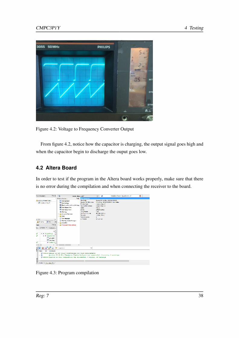
To test the voltage-to-frequency converter, oscillator device is used. The probe will
connect the output of the converter and the oscillator. A saw-tooth waveform will be
shown in the oscilloscope along with the temperature transducer to prove that it works
properly.
Reg: 7 37
CMPC3P1Y 4 Testing
Figure 4.2: Voltage to Frequency Converter Output
From figure 4.2, notice how the capacitor is charging, the output signal goes high and
when the capacitor begin to discharge the ouput goes low.
4.2 Altera Board
In order to test if the program in the Altera board works properly, make sure that there
is no error during the compilation and when connecting the receiver to the board.
Figure 4.3: Program compilation
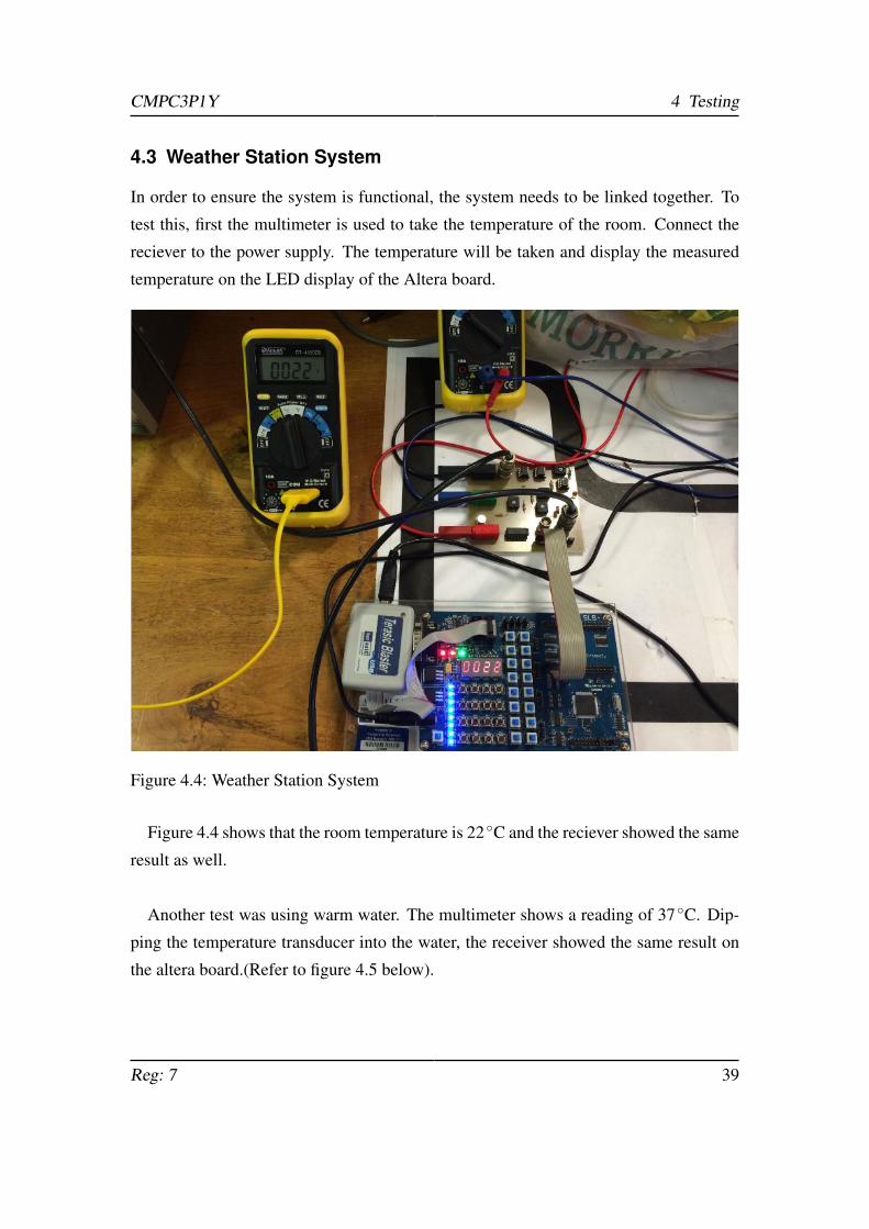
Reg: 7 38
CMPC3P1Y 4 Testing
4.3 Weather Station System
In order to ensure the system is functional, the system needs to be linked together. To
test this, first the multimeter is used to take the temperature of the room. Connect the
reciever to the power supply. The temperature will be taken and display the measured
temperature on the LED display of the Altera board.
Figure 4.4: Weather Station System
Figure 4.4 shows that the room temperature is 22C and the reciever showed the same
result as well.
Another test was using warm water. The multimeter shows a reading of 37C. Dip-
ping the temperature transducer into the water, the receiver showed the same result on
the altera board.(Refer to figure 4.5 below).
Reg: 7 39

CMPC3P1Y 5 Conclusion
Figure 4.5: Weather Station System
5 Conclusion
To conclude, the objectives that was set out at the beginning of the project are met
respectively. All the requirements of the specifications are covered successfully. The
designed receiver can read the temperature and shows the results on the LED display of
the Altera board. This proves that the weather station is fully functional.
Although the weather station is operational, there were a lot of challanges encoun-
tered during the design and development of the weather station. Initially, the tempera-
ture circuit and voltage-to-frequency converter was separated into two individual circuit.
Then the temperature circuit was tested and it produced a positive voltage. The voltage-
to-frequency converter require a negative input. However, during testing, the output of
the temperature circuit needs to be a negative voltage but it was hard to change or add
other components on the temperature circuit since it has been soldered on the circuit
board. When the temprature circuit was connected to the converter, the device was not
Reg: 7 40

CMPC3P1Y 5 Conclusion
working at all.
To fix this, an inverting amplifier component was added to the circuit and the output
gaves a negative voltage. Since the voltage-to-frequency converter circuit was work-
ing properly, both circuit was connected and the device is now functional. A new PCB
containing both temperature circuit and voltage-to-frequency converter needed to be re-
manufactured.
Some of other problems were due to lack of knowledge and experience when pro-
gramming the Altera board. A lot of time has been invested on research especially on
studying how frequency counter works and applying that knowledge into programming
the altera board. During the testing, a series of trial and error was applied to make the
program work well while keeping in mind the limited time given for the project.
5.1 Evaluation
The aim of this section is to provide the outcome of the project, in terms of the perfor-
mance of the system, problem encountered, accomplishments and improvement through-
out the process of the project. The system can be analysed as a whole or individually.
5.1.1 Successes
A fully functional device was developed and tested which shows that the requirement
and specifications of the device were met as well. Difficulties encountered during the
process were overcome by research. It can be either practical research or theoretical
research. If there is more time given, the design can be improved or modified. This is
will be futher explain in the next section.
Reg: 7 41
CMPC3P1Y 5 Conclusion
5.2 Changes made and Further work
5.2.1 Weather Station Receiver
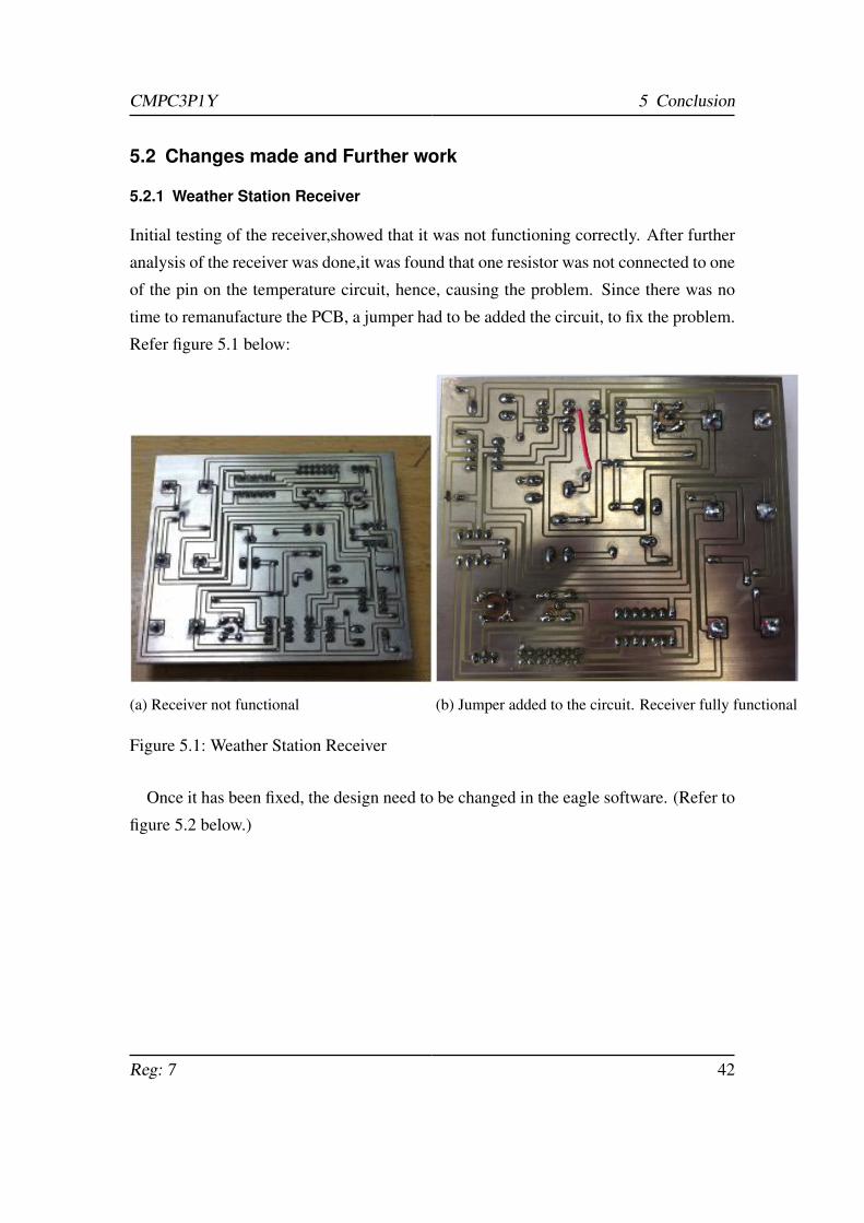
Initial testing of the receiver,showed that it was not functioning correctly. After further
analysis of the receiver was done,it was found that one resistor was not connected to one
of the pin on the temperature circuit, hence, causing the problem. Since there was no
time to remanufacture the PCB, a jumper had to be added the circuit, to fix the problem.
Refer figure 5.1 below:
(a) Receiver not functional (b) Jumper added to the circuit. Receiver fully functional
Figure 5.1: Weather Station Receiver
Once it has been fixed, the design need to be changed in the eagle software. (Refer to
figure 5.2 below.)
Reg: 7 42

CMPC3P1Y 5 Conclusion
Figure 5.2: New PCB design with changes.
More improvements can be made to the circuit, for example, the AD590. Currently
the component cannot be fully submerged into the water as it will cause short circuit.
So it is beneficial to modify the components to it waterproof.
Another improvement is to make a portable receiver by using battries instead of con-
necting it directly to the power supply.
Since the completed device will be exposed to the weather changes and will need to be
placed outside, waterproof casing will be needed to protect the device from rain or snow.
In the future, Arduino or Raspberry Pi devices can be added to this Weather Station
and the temperature can be send to the computer wirelessly.
Reg: 7 43
CMPC3P1Y REFERENCES
References
AD590 Data sheet (2006). 2-terminal ic temperature sensor (ad590 data sheet). https:
// www.physics.rutgers.edu/ ugrad/ 327/ AD590.pdf .
Analog Devices (2009). High precision 10 v ic reference datasheet. http:// www.analog.
com/ static/ imported-files/ data_sheets/ AD581.pdf .
Asque, C. (2012). Pcb guidelines. https:// learn.uea.ac.uk/ bbcswebdav/ pid-919133-dt-
content-rid-691040_1/ courses/ CMPE2D01-12/ Guidelines2.pdf .
Circuits And System module and Digital System Design (2013). Circuits and system
module and digital system design. http:// www.3yp.cmp.uea.ac.uk .
Dioszegi, G. and Nagy, J. (2008). Ne555 timer sparks low-cost voltage-to-frequency
converter.
Floyd, T. L. and Buchla, D. M. (1995). electronics fundamentals. Prentice Hall.
Haresh Khemani and Lamar Stonecypher (2013). Thermocouple. http:
// www.brighthubengineering.com/ manufacturing-technology/ 53682-what-is-a-
thermocouple-how-thermocouple-works/ .
Hewes, John (2014). 74162 decade counters with synchronous reset. http://
electronicsclub.info/ 74series.htm#74162.
Innovative Sensor Technology (2013). Resistance temperature detector (rtd). http://
www.azom.com/ article.aspx?ArticleID=5573.
Kleitz, W. and Kleitz, W. (1996). Digital electronics: a practical approach.
Leach, D. P. and Malvino, A. P. (1994). Digital Principles and Applications.
Glencoe/McGraw-Hill.
Miller, R. L. (1939). Fractional-frequency generators utilizing regenerative modulation.
Proceedings of the IRE, 27(7):446–457.
Reg: 7 44

CMPC3P1Y REFERENCES
Omega Engineering Inc (2013). Introduction to thermistors. http:// www.omega.com/
prodinfo/ thermistor.html .
Surtell, T. (2013). Digital electronics. http:// anorien.csc.warwick.ac.uk/ mirrors/ CTAN/
graphics/ pgf/ contrib/ pgfgantt/ pgfgantt.pdf . 13/02/2007.
System Level Solutions (2005). Altera elt ii reference manual. http:// webuser2.unicas.
it/ elettronica/ iannuzzo/ Ausilii/ rm_ELT_II.pdf .
Tektronix (2000). Oscilloscope fundamentals. http:// circuitslab.case.edu/ manuals/
Oscilloscope_Fundamentals_-_Tektronix.pdf .
Texas Instruments (1972). 74139 dual 2-line to 4-line datasheet. http:// www.ti.com/ lit/
ds/ symlink/ sn74ls139a.pdf .
Texas Instruments (1974). Bcd-to-seven-segment decoders/drivers datasheet. http://
www.ti.com/ lit/ ds/ symlink/ sn74ls47.pdf .
Texas Instruments (1976). Register datasheet. http:// www.ti.com/ lit/ ds/ symlink/
sn74ls173a.pdf .
Texas Instruments (2002). Hex schmitt-trigger inverter datasheet. http:// www.ti.com/ lit/
ds/ sdls049b/ sdls049b.pdf .
United Electric Controls (2013). Temperature sensors. http:// www.ueonline.com/
products/ fp_tempsensors.shtml .
Young, T. (1981). Linear integrated circuits. New York, John Wiley and Sons, 1981. 507
p, 1.
zmashiah (2013). Wireless outdoor arduino weather station with pc logging and
graphs. http:// www.instructables.com/ id/ Wireless-outdoor-Arduino-weather-station-
with-PC-l/ .
Reg: 7 45


![EG Robotics Arduino Weather Station Instruction …ARDUINO WEATHER STATION INSTRUCTION MANUAL] EG Robotics Manual | Interested LLC 2013 | 1 | Page EG Robotics Arduino Weather Station](https://static.documents.pub/doc/80x56/5ab679477f8b9a1a048dc925/eg-robotics-arduino-weather-station-instruction-arduino-weather-station-instruction.jpg)


