Multisim is • a schematic capture, • a simulation program for analog, digital and mixed analog/digital circuits, • and is one application program of the National Instruments “Circuit Design Suite”, which also includes printed circuit board design tools What is Multisim?
Transcript
Multisim is
• a schematic capture,
• a simulation program for analog, digital and mixed
analog/digital circuits,
• and is one application program of the National Instruments
“Circuit Design Suite”, which also includes printed circuit
VeriStand is a software for developing advanced real-time test applications.
By importing simulation models and control algorithms, you can easily interface
your hardware-in-the-loop system with the real world.
Multisim, an advanced, intuitive and practical SPICE simulation environment,
designed for analysis and reporting of measured data.
To download the software and activate it, please refer to the attached file.
For students activation keys are
available:
on http://delphi.uniroma2.it
in the section “attivazione altri servizi”.
How to Download and Install NI Multisim
Introduction to Multisim: Learn to Capture,
Simulate, and Layout in Less Than 30
Minutes
Publish Date: Sep 02, 2014
http://www.ni.com/tutorial/10710/en/
Overview
NI Multisim is a powerful schematic capture and simulation
environment that engineers, students, and professors can use to
simulate electronic circuits and prototype Printed Circuit Boards (PCBs).
This article shows you how to capture,simulate, and layout your first
design in Multisim.
The example circuit in the article is an amplifier circuit. This non-inverting
operational amplifier configuration consists of
one active component (the operational amplifier) and
two passive resistor components that will be used to complete the
feedback network to provide gain in this circuit.
Table of Contents
1. Introduction
2. Part A: Selecting Components
3. Part B: Wiring the Schematic
4. Part C: Simulating the Circuit
5. Part D: Transferring to PCB Layout
6. Part E: Routing the Board
Table of Contents
1. Introduction
2. Part A: Selecting Components
3. Part B: Wiring the Schematic
4. Part C: Simulating the Circuit
5. Part D: Transferring to PCB Layout
6. Part E: Routing the Board
1. IntroductionFor this introductory example, you will simulate a standard non-inverting
operational amplifier circuit (shown in Figure 1). The gain of this non-
inverting amplifier is calculated by the expression Gain = 1 + R1/R2.
Therefore, if R1 = R2, then the gain is equal to 2, which you will verify when
you run interactive simulation in Multisim.
Table of Contents
1. Introduction
2. Part A: Selecting Components
3. Part B: Wiring the Schematic
4. Part C: Simulating the Circuit
5. Part D: Transferring to PCB Layout
6. Part E: Routing the Board
2. Part A: Selecting ComponentsStart by drawing your schematic in the Multisim environment.
1. Open Multisim by selecting Start and clicking Ni Multisim 14.1
2. Select Place»Component. The Select a Component window appears (also known as the Component Browser), as shown in Figure 2.
Figure 2
The Component Browser organizes the database components into three logical
levels. The Master Database contains all shipping components in a read-only
format. The Corporate Database is where you can save custom components to be
shared with colleagues. Finally, the User Database is where custom components
are saved that can be used only by the specific designer.
The components (or parts) are organized into Groups and Families to intuitively and
logically group common parts together and make searching easier and more
effective.
The Component Browser shows the component name, symbol, functional
description, model, and footprint all in a single popup.
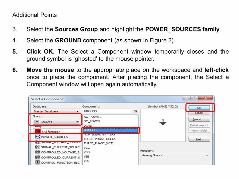
Additional Points
3. Select the Sources Group and highlight the POWER_SOURCES family.
4. Select the GROUND component (as shown in Figure 2).
5. Click OK. The Select a Component window temporarily closes and the
ground symbol is ‘ghosted’ to the mouse pointer.
6. Move the mouse to the appropriate place on the workspace and left-click
once to place the component. After placing the component, the Select a
Component window will open again automatically.
Additional Points
7. Go to the Sources Group again and highlight the POWER_SOURCES
Family (if not already highlighted from the previous selection).
8. Select the DC_POWER component.
9. Click OK. The Select a Component window temporarily closes and the
ground symbol is ‘ghosted’ to the mouse pointer.
10. Place the DC_POWER component on the schematic.
11. Repeat steps 9, 10 to place a second DC_POWER component.
Additional Points
• Without a power and ground your simulation cannot run.
• If you need multiple components you can repeat the placement steps as shown or
place one component and use copy (Ctrl+C) and paste (Ctrl+V) to place additional
components as needed. By default, the Select a Component window keeps
returning as a pop-up until you have completed placing your components.
• Close the window to return to the schematic entry window.
Now place the remaining circuit components using the techniques discussed in the
previous steps.
12. Select the Analog Group and
the OPAMP family.
13. Type AD712 in the Component
field.
14. Select the AD712SQ/883B component, as shown in the figure
15. Place section A of AD712SQ/883B component in the workspace area.
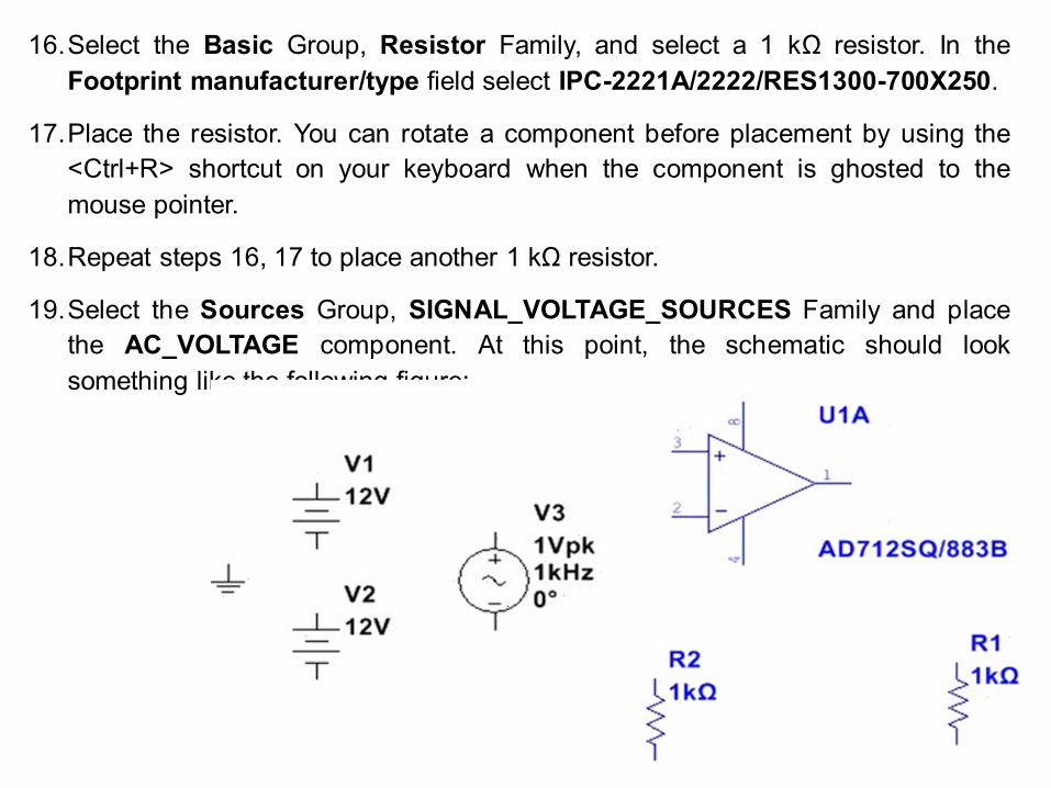
16.Select the Basic Group, Resistor Family, and select a 1 kΩ resistor. In the
Footprint manufacturer/type field select IPC-2221A/2222/RES1300-700X250.
17.Place the resistor. You can rotate a component before placement by using the
<Ctrl+R> shortcut on your keyboard when the component is ghosted to the
mouse pointer.
18.Repeat steps 16, 17 to place another 1 kΩ resistor.
19.Select the Sources Group, SIGNAL_VOLTAGE_SOURCES Family and place
the AC_VOLTAGE component. At this point, the schematic should look
something like the following figure:
Table of Contents
1. Introduction
2. Part A: Selecting Components
3. Part B: Wiring the Schematic
4. Part C: Simulating the Circuit
5. Part D: Transferring to PCB Layout
6. Part E: Routing the Board
Part B: Wiring the SchematicMultisim determines the functionality of the mouse pointer by position of mouse.
Begin wiring by moving the mouse pointer close to a pin of a component.
The mouse appears as a crosshair rather than the default mouse pointer.
1. Place an initial wire junction by clicking on the pin/terminal of the part (in
this case, the output pin of the opamp).
2. Complete the wire by moving the mouse to another terminal or justdouble-click to anchor the termination point of the wire to a floatinglocation somewhere in the schematic window.
3. Create a copy of the ground symbol using Copy <Ctrl+C> and Paste
<Ctrl+V>.
4. Complete the wiring as shown in Figure.
Do not worry about the labeled numbers
on the wires (also called nets).
The last key step is to connect the power supply terminals to the positive and
negative power rails of the opamp via a virtual connection using On-page
connectors.
5. Select Place»Connectors»On-page connector and connect it to the positiveterminal of the V1 power supply. The On-page Connector window will open.
6. Select the +V connector in the Available connectors list and click OK.
7. Select another On-page connector and connect it to terminal 8 of the opamp. TheOn-page Connector window will open again.
The positive terminal of the V1 DC power supply is now connected to pin 8 of theopamp via a virtual connection.
8. Select the +V connector in the Available connectors list and click OK.
9. Repeat steps 6 to 8 to connect the negative terminal of V2 to pin 4 of the opamp.
Name the On-page connector –V. The schematic should now look like the figure.
Table of Contents
1. Introduction
2. Part A: Selecting Components
3. Part B: Wiring the Schematic
4. Part C: Simulating the Circuit
5. Part D: Transferring to PCB Layout
6. Part E: Routing the Board
Part C: Simulating the Circuit• You are now ready to run an interactive Multisim simulation; however, you need
a way to visualize the data.
• Multisim provides instruments to visualize the simulated measurements.
Instruments can be found on the right menu bar and are indicated by the following
icons.
1. Select the Oscilloscope from the menu and place this onto the schematic.
2. Wire the Channel A and Channel B terminals of the Oscilloscope to both the
input and output of the amplifier circuit.
3. Place a ground component and connect it to the negative terminals of the
Oscilloscope.
4. Right-click the wire connected to Channel B and select Segment color.
5. Select a shade of blue and click the OK button. The schematic should look like
Figure .
6. Select Simulate»Run to start the simulation.
7. Double-click on the Oscilloscope to open its Front Panel and observe the simulation results. The input signal should be amplified by a factor of 2.
8. Stop the simulation by pressing the red stop button in the simulation toolbar.
Table of Contents
1. Introduction
2. Part A: Selecting Components
3. Part B: Wiring the Schematic
4. Part C: Simulating the Circuit
5. Part D: Transferring to PCB Layout
6. Part E: Routing the Board
Part D: Transferring to PCB LayoutWe are now ready to transfer the Multisim design to Ultiboard for PCB layout.
Sources (power, signal) and ground are virtual components, therefore, they
cannot be transferred to Ultiboard. Also, all components must include footprint
information. It is a good practice to replace power sources and ground with
connectors.
1. Remove V1, V2, V3 and the Oscilloscope from the schematic. Do not
remove the On-page connectors.
2. Open the Component Browser, and place the 282834-4 terminal block fromthe Connectors Group, TERMINAL_BLOCKS Familly. This connector will beused to connect the power supplies (+V, -V).
3. Connect pin 1 of the connector to the +V On-pageconnector, pin 4 to the –V On-page connector, andpins 2 and 3 to ground, as shown in the figure
4. Place another 282834-4 terminal block on the workspace. This
connector will be used to connect the input and output signals.
5. Connect pin 1 of the connector to pin 3 (input) of the opamp.
6. Connect pin 2 of the connector to pin 1 (output) of the opamp.
7. Connect pin 3 of the connector to ground. The schematic will look like
the next figure.
8. Select Transfer»Transfer to Ultiboard»Transfer to Ultiboard 13.0 and save
the netlist file. Ultiboard will open automatically.9. Click OK to accept all the actions listed in the Import Netlist window. Ultiboard
will create a default board outline. Note that all the parts are placed outside ofthe board outline and the yellow lines (ratsnests) identifying the connectionsbetween pins, as shown in Figure.
10.Locate the Design Toolbox on the left side of the
screen.
11.Select the Layers tab and double-click Board
Outline to enable this layer, as shown in the
figure.
For this exercise we will use a 2x2 inch board.
Follow these steps to resize the board outline.
The Layers tab of the Design Toolbox is where you move between layers of your
design and control the appearance of layers.
12 Go to the toolbar area and locate the Select toolbar, refer to the following figure.
The Select toolbar contains the functions used to control selection filters. In other
words, these filters control what can be selected by the mouse pointer.
13.Disable all the filters except Enable selecting other objects.
14.Double-click the board outline on the workspace area to open the Rectangle
Properties window.
15.Select the Rectangle tab, change Units to inch and enter 2 for Width and 2 for
Height.
16.Click OK.
Table of Contents
1. Introduction
2. Part A: Selecting Components
3. Part B: Wiring the Schematic
4. Part C: Simulating the Circuit
5. Part D: Transferring to PCB Layout
6. Part E: Routing the Board
Part E: Routing the BoardPlace components inside the board.
1. Go to the Select toolbar and disable all the filters except Enable selecting
parts.
2. Drag part J2 and drop it inside the Board Outline. You can rotate parts by
using the <Ctrl+R> shortcut.
3. Place the rest of the parts inside the Board Outline, use Figure as guidance.
For this exercise you will place traces on both, the Copper Top and Copper
Bottom layers.
4. Double-click the Copper Top layer in the Design Toolbox.
5. Select Place»Line.
6. Locate part U1 (the opamp). Note that pin 1 needs to be connected to R1, as
indicated by the ratsnest.
7. Click pin 1 of part U1, draw a line to R1
and click its pin to finish the trace. Press
Esc to exit the routing mode. The trace
will look like the following figure.
8. Double-click the the Copper Bottom layer in the Design Toolbox.
9. Select Place»Line.10.Click pin 2 of part U1, draw a line to R1 and click its pin to finish the trace.
Press Esc to exit the routing mode. Note that the color of the trace is red,which is the color configure for the Copper Bottom layer.