Organizing Committee Co-Sponsored by: The 37th Annual Spring Symposium May 26, 2010 EECS Building, University of Michigan, Ann Arbor, Michigan, USA White-Light LEDs for Automotive and General Lighting Applications P.-C. Ku (Chair) Terrence Brown Pilar Herrera-Fierro Michael Lukitsch Hiroko Ohtani American Vacuum Society Michigan Chapter
Transcript
Organizing Committee Co-Sponsored by:
The 37th Annual Spring Symposium
May 26, 2010
EECS Building, University of Michigan, Ann Arbor, Michigan, USA
White-Light LEDs for Automotive and General Lighting Applications
P.-C. Ku (Chair) Terrence Brown Pilar Herrera-Fierro Michael Lukitsch Hiroko Ohtani
American Vacuum Society Michigan Chapter
White-Light LEDs
for Automotive and General Lighting Applications
37th Annual Spring Symposium
Michigan Chapter of the American Vacuum Society
Co-Sponsored by University of Michigan
Office of Vice President for Research College of Engineering
Department of Electrical and Computer Eng. Michigan Memorial Phoenix Energy Institute
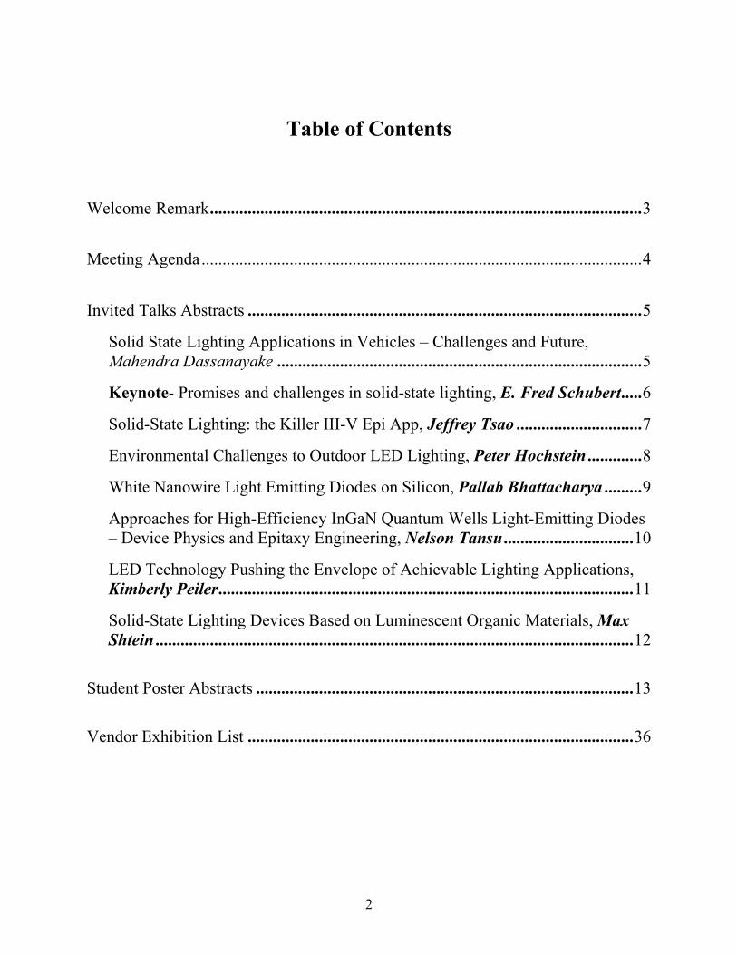
Solid State Lighting Applications in Vehicles – Challenges and Future, Mahendra Dassanayake ....................................................................................... 5
Keynote- Promises and challenges in solid-state lighting, E. Fred Schubert ..... 6
Environmental Challenges to Outdoor LED Lighting, Peter Hochstein ............. 8
White Nanowire Light Emitting Diodes on Silicon, Pallab Bhattacharya ......... 9
Approaches for High-Efficiency InGaN Quantum Wells Light-Emitting Diodes – Device Physics and Epitaxy Engineering, Nelson Tansu ............................... 10
LED Technology Pushing the Envelope of Achievable Lighting Applications, Kimberly Peiler ................................................................................................... 11
Solid-State Lighting Devices Based on Luminescent Organic Materials, Max Shtein .................................................................................................................. 12
Vendor Exhibition List ............................................................................................ 36
3
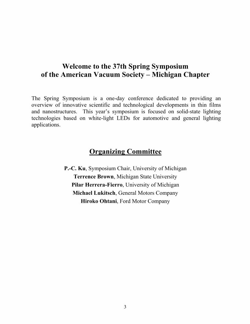
Welcome to the 37th Spring Symposium of the American Vacuum Society – Michigan Chapter
The Spring Symposium is a one-day conference dedicated to providing an overview of innovative scientific and technological developments in thin films and nanostructures. This year’s symposium is focused on solid-state lighting technologies based on white-light LEDs for automotive and general lighting applications.
Organizing Committee
P.-C. Ku, Symposium Chair, University of Michigan
Terrence Brown, Michigan State University Pilar Herrera-Fierro, University of Michigan Michael Lukitsch, General Motors Company
Hiroko Ohtani, Ford Motor Company
4
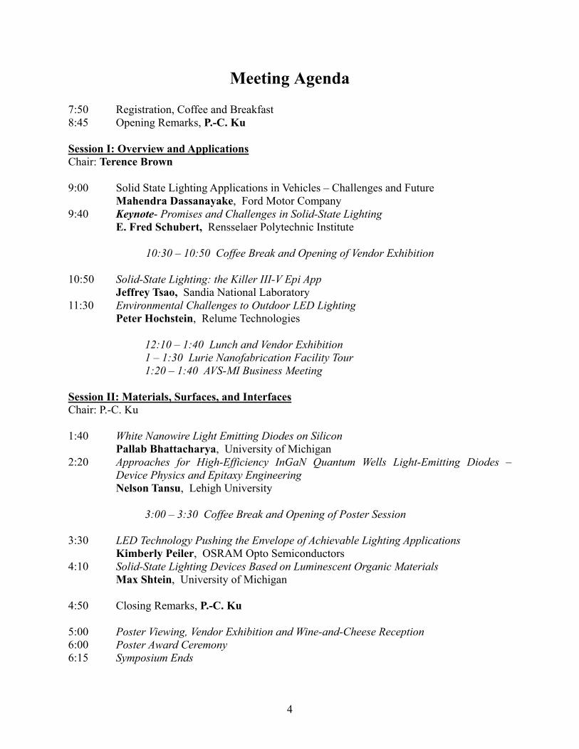
Meeting Agenda
7:50 Registration, Coffee and Breakfast 8:45 Opening Remarks, P.-C. Ku Session I: Overview and Applications Chair: Terence Brown 9:00 Solid State Lighting Applications in Vehicles – Challenges and Future Mahendra Dassanayake, Ford Motor Company 9:40 Keynote- Promises and Challenges in Solid-State Lighting E. Fred Schubert, Rensselaer Polytechnic Institute
10:30 – 10:50 Coffee Break and Opening of Vendor Exhibition 10:50 Solid-State Lighting: the Killer III-V Epi App Jeffrey Tsao, Sandia National Laboratory 11:30 Environmental Challenges to Outdoor LED Lighting Peter Hochstein, Relume Technologies
12:10 – 1:40 Lunch and Vendor Exhibition 1 – 1:30 Lurie Nanofabrication Facility Tour 1:20 – 1:40 AVS-MI Business Meeting
Session II: Materials, Surfaces, and Interfaces Chair: P.-C. Ku 1:40 White Nanowire Light Emitting Diodes on Silicon Pallab Bhattacharya, University of Michigan 2:20 Approaches for High-Efficiency InGaN Quantum Wells Light-Emitting Diodes –
Device Physics and Epitaxy Engineering Nelson Tansu, Lehigh University
3:00 – 3:30 Coffee Break and Opening of Poster Session 3:30 LED Technology Pushing the Envelope of Achievable Lighting Applications Kimberly Peiler, OSRAM Opto Semiconductors 4:10 Solid-State Lighting Devices Based on Luminescent Organic Materials Max Shtein, University of Michigan 4:50 Closing Remarks, P.-C. Ku 5:00 Poster Viewing, Vendor Exhibition and Wine-and-Cheese Reception 6:00 Poster Award Ceremony 6:15 Symposium Ends
5
Solid State Lighting Applications in Vehicles – Challenges and Future
Mahendra Dassanayake
Ford Motor Company Over last 20 years solid state technology has evolved from indication applications to illumination application along with the progress of the Light Emitting Diode. This trend has also followed the auto industry due to ever growing demand for creating uniqueness among brands in terms of styling, feature function content and ever-increasing need for quality leadership.. Basic elements of light and heat management will be discussed as it relates to illumination design in vehicle applications. Techniques and technologies that have evolved in geometrical Optics in shaping perception and functionality engineering will be the fundamental basis for the discussion. As the 3rd most consumer of power in the vehicles, adaptation of solid state lighting in vehicles will embraced, provided it can deliver the cost of light at an affordable business case. Spectral implications and cost of light in automotive applications will also be discussed relative to electrification trends in the auto industry. Solid state lighting has opened a new era in low-current integration of sensing and lighting that will lead comfort,/convenience and safety/security applications for years to come. Biography: Dr. Mahendra Dassanayake, is a Technical Leader in Ford Motor Company working on product integration of optical and lighting devices in next generation vehicle applications. He has over fifteen years of experience in design and development of advance optical and lighting devices for the auto-industry. At Ford he pioneered the implementation of several new headlamps, tail lamp concepts and developed new interior cockpit device concepts. He was a key driver in implementing InGaN based white LEDs for vehicle interior applications as well. Institutionalizing digital photometry, for evaluating visual performance of interior and exterior lighting devices is another area of his interests. He obtained is Ph.D. Degree, in Electrical Engineering at the State University of New York at Buffalo in 1984. After his graduate work, he also worked as a product design engineer and a Technical specialist in the Ford Automotive Components Division till the fall of 1999. Currently he has over 40 patents and inventions in automotive lighting and instrumentation.
6
Promises and Challenges in Solid-State Lighting E. Fred Schubert
Rensselaer Polytechnic Institute, Troy NY 12180 Lighting technologies based on semiconductor light-emitting diodes (LEDs) offer unprecedented promises that include three major benefits: (i) Gigantic energy savings enabled by efficient conversion of electrical energy to optical energy; (ii) Substantial positive contributions to sustainability through reduced emissions of global-warming gases, acid-rain gases, and toxic substances such as mercury; and (iii) The creation of new paradigms in lighting driven by the unique controllability of solid-state lighting sources. Due to the powerful nature of these benefits, the transition from conventional lighting sources to solid-state lighting is virtually assured. This presentation will illustrate the new world of lighting including the pervasive changes to be expected in lighting, displays, communications, and biotechnology. The presentation will also address the formidable challenges that must be addressed to continue the further advancement of solid-state lighting technology. These challenges offer opportunities for research and innovation. Specific challenges include light management, carrier transport, and optical design. We will present some innovative approaches in order to solve known technical challenges faced by solid-state lighting. These approaches include the demonstration and use of new optical thin-film materials with a continuously tunable refractive index. These approaches also include the use of polarization-matched structures that reduce the polarization fields in GaInN LEDs and the hotly debated efficiency droop, that is, the decreasing LED efficiency at high currents. Biography: E. Fred Schubert received his Ph.D. in Electrical Engineering from the University of Stuttgart (Germany) in 1986. From 1981 to 1985 he worked on compound semiconductor crystal growth at the Max Planck Institute for Solid State Research, Stuttgart, as a Member of Scientific Staff. During 1985 to 1995, he was a Post-doctoral Fellow, Member of Technical Staff, and Principal Investigator at AT&T Bell Laboratories in Holmdel and Murray Hill, New Jersey. In 1995, he entered academia at Boston University as a Professor of Electrical Engineering. He joined Rensselaer Polytechnic Institute in 2002 where he is the Wellfleet Senior Constellation Professor of the Future Chips Constellation with appointments in the Electrical Engineering Department and Physics Department. From 2008–2009, he served as the Director of the Smart Lighting Engineering Research Center (ERC) awarded by the National Science Foundation to Rensselaer Polytechnic Institute in 2008.
Dr. Schubert has made pioneering contributions to the field of compound semiconductor materials and devices in particular to the fields of alloy broadening, delta-doping, resonant-cavity light-emitting diodes, enhanced spontaneous emission in Er-doped Si/SiO2 microcavities, elimination of unipolar heterojunction band discontinuities, p-type superlattice doping in AlGaN, photonic-crystal light-emitting diodes, polarization-enhanced ohmic contacts, omni-directional reflectors, low-refractive index materials, anti-reflection coatings, light-emitting diodes with remote phosphors, and solid-state lighting.
He is inventor or co-inventor of 30 US patents and has authored or co-authored more than 275 publications. He authored the books Doping in III–V Semiconductors (1993), Delta Doping in Semiconductors (1996), and the first and second edition of Light-Emitting Diodes (2003 and 2006); the latter book was translated into Russian and Japanese. Awards include Senior Member IEEE (1993); Literature Prize of Verein Deutscher Elektrotechniker for book “Doping in III–V semiconductors” (1994); Fellow SPIE (1999); Alexander von Humboldt Senior Research Award (1999); Fellow IEEE (1999); Fellow OSA (2000); Boston University Provost Innovation Award (2000); Discover Magazine Award for Technological Innovation (2000); R&D 100 Award for RCLED (2001); Fellow APS (2001); RPI Trustees Award for Faculty Achievement (2002 and 2008); Honorary membership in Eta Kappa Nu (2004); 25 Most Innovative Micro- and Nano-Products of the Year Award of R&D Magazine (2007); and the SCIENTIFIC AMERICAN 50 AWARD (2007).
7
Solid-State Lighting: the Killer III-V Epi App Jeffrey Y. Tsao
Principal Member of Technical Staff, Physical, Chemical and Nano Sciences Center, Sandia National Laboratories, P.O. Box 5800, Albuquerque, NM 87185-1421, USA.
E-mail: [email protected] Throughout its history, lighting technology has made tremendous progress: the efficiency with which power is converted into usable light has increased 2.8 orders of magnitude over three centuries. This progress has, in turn, fueled large increases in the consumption of light and productivity of human society. In this talk, we review an emerging new technology, solid-state lighting: its frontier performance potential; the underlying advances in physics and materials that might enable this performance potential; the resulting energy consumption and human productivity benefits; and the impact on worldwide III-V epi manufacture. Biography: Jeffrey Y. Tsao is currently a Principal Member of Technical Staff at Sandia National Laboratories, and Chief Scientist of its Energy Frontier Research Center for Solid-State-Lighting Science. His work involves integrated science, technology and economic modeling in Solid-State Lighting and other areas. He is also exploring network models of knowledge production – a new approach to the field of “evolutionary epistemology.” During 2000-2001 Jeff served as vice-president of R&D at E2O Communications, Inc., a fast-growing U.S.-based pre-IPO fiber communications components company. During 1993-2000, he served as manager of various technical groups at Sandia National Laboratories, mostly in the area of compound semiconductor materials and devices. In 1998, he took a sabbatical at the Institute of Materials Research and Engineering in Singapore, where he developed and gave a series of twelve lectures on compound semiconductor epitaxy. Jeff has authored or co-authored over 100 publications, holds 9 U.S. patents, and is author of a 1993 research monograph “Materials Fundamentals of Molecular Beam Epitaxy.” He co-authored an influential 1999 white paper outlining the potential of Solid-State Lighting, and edited the comprehensive 2002 U.S. Solid-State Lighting Roadmap. He helped the Office of Basic Energy Science coordinate two influential workshops and reports: one in 2005 on “Basic research needs in solar energy utilization,” and another in 2006 on “Basic research needs in solid-state lighting.” He has been active in various professional societies, including the Materials Research Society, for which he has co-chaired two symposia, was general co-chair of the Spring 1995 meeting, served for several years on the program committee, and during 1998-2000 coordinated the graduate student awards. He was elected Fellow of the American Physical Society in 1996, and Fellow of the American Association for the Advancement of Science in 2009.
8
Environmental challenges to outdoor LED lighting Peter A. Hochstein
CTO, Relume Technologies, Inc., 925 N. Lapeer Rd., Bldg. B, Oxford, MI 48371 USA White, high power, phosphor converted LEDs are beginning to show up in roadway and area lighting fixtures. Ann Arbor has had more experience with such LED lamps than any other city. While the energy savings are clearly documented, a reasonable return on investment is only possible if the LEDs live up to their claims of extraordinary long life. As solid state devices, exposed to a wide range of environmental conditions, LEDs must be carefully configured in order to prevent early degradation. Excessive operating temperature has long been recognized as a primary cause of light diminution. A second, more challenging degradation mechanism is now apparent as certain organic vapors have been shown to affect the LED phosphors and sometimes the actual die. These effects will be discussed in detail and operating samples showing degraded properties will also be demonstrated.
9
White Nanowire Light Emitting Diodes on Silicon P. Bhattacharya*, W. Guo, and M. Zhang
Solid-State Electronics Laboratory, Department of Electrical Engineering and Computer Science, University of Michigan, Ann Arbor, MI 48109-2122, USA
*E-mail: [email protected], Phone: 734-763-6678; Fax: 734-763-9324 We have investigated catalyst-free MBE growth of (In)GaN nanowires directly on (001) silicon, n- and p-doping of the nanowires, and the characteristics of LEDs made with the nanostructures. The nanowires were grown on (001) silicon substrates by plasma-assisted MBE. To study the growth mechanism, GaN nanowires were grown under different conditions. To achieve different emission wavelengths, InGaN nanowires with varied indium compositions were synthesized at 550 C. In addition, the indium composition was changed gradually along the nanowires during the growth to obtain broad and “white” emission. InGaN/GaN nanowire heterostructures and nanowires with InGaN/GaN quantum dots were also grown and characterized.
The structural characteristics of the nanowires were studied using FE-SEM and TEM. High density (~ 1011 cm-2) nanowires are grown with diameters ranging from 10 to 50nm, and they exhibit excellent uniformity in length. A HR-TEM study indicates that the nanowires are relatively defect-free, and the c-plane is normal to the growth direction. Room temperature PL spectra ranging from ultraviolet to red are obtained from nanowires with different indium compositions. A broad emission with 140nm full-width-at-half-maximum (FWHM) was recorded from InGaN nanowires with gradually varied indium composition during epitaxy. An internal quantum efficiency of 30% is derived, assuming that the internal quantum efficiency is 100% at 10K.
Nanowire LED heterostructures consisting of p-type GaN, undoped compositionally graded InGaN and n-type GaN were grown on n-type (100) silicon substrate. The electroluminescence spectrum of the nanowire LED was measured at room temperature. CIE chromaticity coordinates are derived by analyzing the electroluminescence spectrum of the white LEDs under different forward-bias currents. Correlated Color Temperatures (CCT) of 5500K-6500K are also derived from the Planckian locus.
Biography: Pallab Bhattacharya is the Charles M. Vest Distinguished University Professor of Electrical Engineering and Computer Science and the James R. Mellor Professor of Engineering in the Department of Electrical Engineering and Computer Science at the University of Michigan, Ann Arbor. He received the M. Eng. and Ph.D. degrees from the University of Sheffield, UK, in 1976 and 1978, respectively. Professor Bhattacharya was an Editor of the IEEE Transactions on Electron Devices and is Editor-in-Chief of Journal of Physics D. He has edited Properties of Lattice-Matched and Strained InGaAs (UK: INSPEC, 1993) and Properties of III-V Quantum Wells and Superlattices (UK: INSPEC, 1996). He has also authored the textbook Semiconductor Optoelectronic Devices (Prentice Hall, 2nd edition). His teaching and research interests are in the areas of compound semiconductors, low-dimensional quantum confined systems, nanophotonics and optoelectronic integrated circuits. He is currently working on high-speed quantum dot lasers, quantum dot infrared photodetectors, photonic crystal quantum dot devices, and spin-based heterostructure devices. Professor Bhattacharya is a member of the National Academy of Engineering. He has received the John Simon Guggenheim Fellowship, the IEEE (EDS) Paul Rappaport Award, the IEEE (LEOS) Engineering Achievement Award, the Optical Society of America (OSA) Nick Holonyak Award, the SPIE Technical Achievement Award, the Quantum Devices Award of the International Symposium on Compound Semiconductors, the IEEE (Nanotechnology Council) Nanotechnology Pioneer Award, and the TMS John Bardeen Award. He has also received the S.S. Attwood Award, the Kennedy Family Research Excellence Award, and the Distinguished Faculty Achievement Award from the University of Michigan. He is a Fellow of the IEEE, the American Physical Society, the Institute of Physics (UK), and the Optical Society of America.
10
Approaches for High-Efficiency InGaN Quantum Wells Light-Emitting Diodes – Device Physics and Epitaxy
Center for Optical Technologies, Department of Electrical Computer Engineering, Lehigh University, Bethlehem, PA 18015, USA
± Email: [email protected] Energy efficiency and renewable energy technologies have significant importance for achieving sustainable energy systems in modern society. Lighting accounts for more than 22% of the total electrical energy usage in US, and technologies based on solid state lighting (SSL) utilizing semiconductor-based material has tremendous promise to replace the existing lighting devices. As compared to traditional incandescent and fluorescent lamps, SSL is more energy-efficient, reliable, and environmentally-friendly. Once widely used, SSL could lead to the decrease of worldwide electricity consumption for lighting by >50% and reduces total electricity consumption by >10%. Rapid progress in SSL research and development has resulted in the advent of light emitting diodes (LEDs) for general lighting applications. Two major challenges for current state-of-art III-nitride based LEDs are 1) ‘green gap’ issue in InGaN quantum well light-emitting diodes, and 2) ‘efficiency droop’ issue in III-Nitride LEDs resulting in output power quenching at high current injection. In this work, novel approaches to address the major issues related to nitride LEDs will be presented. The studies will include designs, growths, and device characteristics of 1) novel InGaN-based quantum well structures LEDs with enhanced matrix element for realizing green-emitting LEDs devices with high internal quantum efficiency, and 2) novel InGaN QW LEDs device structure with lattice-matched AlInN-barrier structure to suppress efficiency-droop in nitride LEDs. The use of polarization engineering leads to a significant improvement in the radiative efficiency of the InGaN QW LEDs, in particular for addressing the charge separation effect in green-emitting nitride devices. The use of graded-growth-temperature profiling to realize 3-layer staggered InGaN QW LEDs has led to 2-3 times improvement in radiative efficiency, in comparison to that of the conventional InGaN QW LEDs. In addition to the QW engineering approaches, other approaches to improve the efficiency of the nitride LEDs will be discussed as follow: 1) the use of surface plasmon LEDs, 2) new growth approach for dislocation density reduction in GaN semiconductor, and 3) novel approaches for light extraction efficiency improvement of III-Nitride LEDs.
11
LED technology pushing the envelope of achievable lighting applications
Kimberly Peiler
OSRAM Opto Semiconductors The achievable application space for LED technology is ever increasing due to fundamental LED technology advances coupled with system solutions. We will review OSRAM Opto Semiconductors recent technology advances with respect to high performance power LEDs as well as selected solid state and automotive lighting requirements. We will then discuss the latest innovative LED products that have resulted for these markets combining fundamental LED technology and application requirements. Finally a few case study examples integrating these light sources into end systems.
12
Solid state lighting devices based on luminescent organic materials
Max Shtein
Materials Science and Engineering, University of Michigan
The U.S. spends each year nearly $300 billion on electricity for lighting and disposes of 660 million fluorescent tubes, amounting to over 10 metric tons of mercury. Emerging LED-based solid-state lighting technologies attempt to combine efficiency and environmental friendliness, but face significant barriers for scalability and cost-effectiveness. This talk will discuss in detail some of the drivers in the field of solid-state lighting, focusing in particular on issues in organic-based LED research and development. The talk will conclude by discussing novel solid-state, white light architectures based on luminescent organic materials and coatings, which show significant promise for efficient, yet cost-effective and scalable lighting technology. Biography: Prof. Shtein obtained his BS from UC Berkeley and his PhD from Princeton. He has made enabling contributions to the science and technology of organic optoelectronics, including the modeling and demonstration of novel devices and highly scalable methods of device processing. Some of his contributions are currently being commercialized for the fabrication of OLEDs, organic solar cells, and transistors. He has received the Materials Research Society Graduate Student Gold Medal Award, the PRISM-Newport Award of Excellence and Leadership in Photonics and Optoelectonics, the Jon R. and Beverly S. Holt Awards for Excellence in Teaching in 2007, the Presidential Early Career Award for Scientists and Engineers, and the Materials Science and Engineering Department Achievement award.
13
Student Posters
(in alphabetical order of presenter's last name) MSU: Michigan State University
UM: University of Michigan WSU: Wayne State University
No. Author's Name Poster Title School Page
1 Shaurjo Biswas Atmospheric printing of OLEDs for solid state lighting applications
UM 15
2 Mark Chen Graphene Field-Effect Transistors for PH and Biological Sensing
WSU 16
3 Seok-Youl Choi Growth of Al Catalyzed Si Nanowires UM 17 4 Rachel Collino Ion-cut-synthesis of N-implanted GaAs UM 18 5 Tanya Das Modeling Defects in HgCdTe Lateral
Collection APDs UM 19
6 Vaishno Dasika Influence of Dopant Atoms on InAs/GaAs Quantum Dot Electronic States
UM 20
7 Wayne Fung Epitaxial Growth of Ge and Ge/Si Nanowires for Vertical Device Integration
UM 21
8 Anne Itsuno Predicted Performance Improvement of Auger Suppressed High Operating Temperature HgCdTe Photodiodes over p-n Heterojunction Detectors
UM 22
9 Myungkoo Kang FIB-Synthesized Surface Nanostructure Arrays for Negative Index Metamaterials
UM 23
10 Min Kim Metal-Clad Nanolasers UM 24 11 Michael Kuo Nanostructured Semipolar InGaN LEDs for
Solid-State Lighting UM 25
12 Luke Lee Selective area epitaxy for GaN based optoelectronic devices and integration
UM 26
13 Luke Lee Single-molecular sensing using the zeroth-mode optical waveguide
UM 27
14 Steven Morris High-strength electrically conductive fibers and yarns for OLED-based solid-state lighting
UM 28
15 Brian Roberts Broadband Characteristics of Surface Plasmon Enhanced Solar Cells
UM 29
16 Jeffrey Siddiqui Study of CV Characteristics of ALD High-K dielectric ZnO Capacitors
UM 30
14
No. Author's Name Poster Title School Page
17 Michael Tulman New Designs for LWIR/VLWIR FPI UM 31 18 Joshua Veazey Microbial nanowire electronic structure
probed by STM MSU 32
19 Adam Wood Directed Matrix Seeding of Nitride Semiconductor Nanocrystals
UM 33
20 Chung Wu One-step direct transfer of pristine single-walled carbon nanotubes for functional nanoelectronics
UM 34
21 Zhixian Zhou Graphene nanoribbons produced from sonicating graphite in solution for device applications
WSU 35
15
Atmospheric Printing of OLEDs for Solid State Lighting Applications Shaurjo Biswas1, Kevin P. Pipe2, Max Shtein1
1Department of Materials Science and Engineering 2Department of Mechanical Engineering University of Michigan, Ann Arbor
One of the impediments to attaining low-cost, energy efficient, large-area lighting based on small
molecular OLEDs is the cost of depositing the organic emitter layers in high to moderate vacuum. Here we demonstrate the ability to deposit OLEDs in atmosphere, overcoming this processing challenge. Our approach is to use a highly collimated jet of an inert carrier gas mixed with organic vapor impinging onto a substrate, on which the heavier organic molecules selectively condense.1, 2 Importantly, a secondary jet of inert gas coaxially surrounds the primary jet, hydro-dynamically focusing it and shielding the organic vapor from the atmosphere. The guard jet reduces contact between the hot organic vapor and atmospheric oxygen or moisture,3 improving device performance relative to devices printed without the guard jet. In fact, using this approach we achieve equivalent electroluminescence efficiency between atmospherically printed and vacuum-deposited emissive layers.4 1. M. Shtein et al., J. Appl. Phys. 96, 4500 (2004). 2. Y. Sun et al., Appl. Phys. Lett. 86, 113504 (2005). 3. H. Aziz et al., Appl. Phys.Lett. 72, 756 (1998). 4. S. Biswas et al., (App. Phys. Lett., accepted).
d into a two-damental reseally-thick plangraphene an i
2D materialhe sensitivityheir extremelbased biosensonditions. Thaphene FET iisolated from
oltage. In addtion and redors can be use
screening an
h different pHith different p
pH and Bbin Tan1, Yiy
g-Cheng Cheing, 2Department ot MI USA e.edu
dimensional harch and potenne, the electriideal sensing l, its whole y. Neverthelely high sensitsors as well ahis poster repintegrated wi
m the solutiondition, the miduction of bed for a widend electrostati
H. The appliedpH values wer
Biological Syang Zhang1
eng1 of Physics
honeycomb lntial applicatiical conductamaterial for lvolume is e
ess, it is alstivity. It is ouas to optimizeports our expith microfluidn, it is possibicrofluidics inbiological ree pH range (fic gating effe
d voltage is 0re pumped th
Sensing 1, Ming-Wei
attice, has recions. As the cnce of graphelabel-free cheexposed to suso recognizedur goal to elue device strucerimental stu
dics. Since theble to optimizncorporated i
eagents. We from 3-11) wects appear to
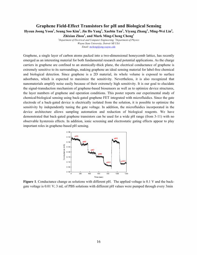
0.1 V and the hrough every 3
Lin2,
cently charge ene is
emical urface d that cidate
ctures, udy of e gate ze the in the
have ith no o play
back-3min
17
Growth of Al Catalyzed Si Nanowires Seok-Youl Choi, Wayne Y. Fung, and Wei Lu
Department of Electrical Engineering and Computer Science, University of Michigan, Ann Arbor, MI 48109, USA
Silicon nanowires have been widely studied as a promising candidate in high-performance
electronics, sensors and solar cells. In most studies, the nanowires were grown using a vapor-liquid-solid (VLS) method employing Au nanoparticles as catalysts. However, Au creates deep defect levels in Si and is not compatible with CMOS processing and may affect the minority carrier lifetime in solar-cell and other device applications. Here, we report the synthesis of Si nanowires at high growth rates (>2 μm/min) on (111) Si substrates using Al as the catalyst. Aluminum can serve as a suitable catalyst for VLS growth since the Al-Si binary phase diagram is similar to that of Au-Si but with a higher eutectic point (577 °C vs 363 °C) at a lower Si concentration (12% vs 19%). In addition, Al is a shallow acceptor in Si and is therefore expected to yield p-type Si nanowires. The use of Al, which can serve as both a catalyst and dopant, is therefore of significant interest for the fabrication of Si nanowire. However, the growth of Si nanowires using Al has proven to be more challenging compared to that obtained with Au due primarily to the reactivity of Al with ambient O2 and H2O, which results in the formation of a surface oxide layer.
In our study, the use of high H2 and SiH4 partial pressures was found to be effective at reducing
problems associated with Al oxidation and nanowire nucleation, enabling growth of high aspect ratio nanowires at temperatures ranging from 490 to 550 °C with minimal tapering of the diameter. The as-grown Si nanowires have diameters in the range of 100 - 200 nm. Due to the high growth rate observed, the Al catalyst is believed to be in the liquid state during the growth. Back-gated current-voltage measurements indicate that the wires are p-type, and these results suggest that Al is incorporated into the Si nanowires. This work demonstrates that Al can serve as an effective catalyst for the growth of large-quantities of Si nanowires with uniform diameter, high growth rate and large aspect ratio.
18
Ion-cut-synthesis of N-implanted GaAs R.R. Collinoa, N.M. Estradaa, B.B. Dickb, M.D. Thoulessa,c, and R.S. Goldmana,d,e
aMaterials Science and Engineering, bNuclear Engineering and Radiological Sciences, cMechanical Engineering, dElectrical Engineering and Computer Science ePhysics
University of Michigan, Ann Arbor, MI 48109
In several semiconductor and oxide systems, light-ion implantation and thermal annealing results in gas bubble formation that may be exploited to achieve thin-film layer transfer in a process termed “ion-cut.” However, this process has only been used for the transfer of unpatterned films; the combination of patterning and layer transfer via ion-cut alone has not been accomplished. It is likely that the simultaneous precipitation of a new phase and bubble formation is not possible in systems with high ion-matrix diffusivity, such as Si:H and GaAs:H.
In contrast, the low ion-matrix diffusivity of GaAs:N apparently enables the simultaneous formation of nanocrystals and gas bubbles,i thereby facilitating the combination of nanostructuring and layer transfer. Thus, we have recently demonstrated the ‘ion-cut-synthesis’ process for the transfer of nanostructured GaAs:N films to Al2O3 and AlN substrates. Ion-cut-synthesis was accomplished via N-ion implantation in GaAs, followed by spin-on glass (SOG) mediated wafer bonding and rapid-thermal annealing. The optimization of this SOG-assisted bonding process led the transfer of GaAs:N films with rms roughness comparable to that reported for low-temperature transfer of crystalline GaAs layers to Si substrates.ii The integration of nanocomposite materials with a variety of substrates coupled with the ability to recycle the donor substrate makes ion-cut-synthesis attractive for high-efficiency, low-cost electronics, optoelectronics, and energy conversion devices.
1 R. R. Collino, B. B. Dick, F. Naab, Y. Q. Wang, M. D. Thouless, and R. S. Goldman, Appl. Phys. Lett. 95, 111912 (2009). 1 E. Jalaguier et al., Electron. Lett. 34, 408 (1998).
19
Modeling Defects in HgCdTe Lateral Collection APDs Tanya Das, Anne Itsuno, Jinyoung Hwang, Jamie Phillips
Department of Electrical Engineering and Computer Science, University of Michigan, Ann Arbor Mercury-Cadmium-Telluride (HgCdTe) Infrared (IR) detectors are useful in a variety of applications including military applications, thermal imaging, and remote sensing. The detectors are implemented in the form of avalanche photodiodes (APDs). APDs are very useful for this application, as they have a high internal gain and correspondingly a high signal-to-noise ratio. Currently, the APD is implemented in a vertical structure, consisting of vertical stacks of the arsenic-doped p-region, absorber region, and boron-doped n-region. In this configuration, the threading dislocations which permeate between device regions are detrimental to device performance. This project aims to reduce the effects of such defects in APDs by implementing a lateral structure, where the three regions are stacked next to each other rather than on top of each other. This lateral APD structure and the defects present between the three regions will be simulated using Sentaurus software. The results of the simulations will enable a better design of lateral collection HgCdTe photodiodes and understanding of the role of defects on device performance.
20
Influence of Dopant Atoms on InAs/GaAs Quantum Dot Electronic States V.D. Dasika,(1) J. C. Dibbern,(2) A.M. Dangelewicz,(2) R.S. Goldman,(1),(2) M. Holub,(1) and
P.K.Bhattacharya (1) (1) Department of Electrical Engineering and Computer Science, University of Michigan,
(2) Department of Materials Science and Engineering, University of Michigan, Ann Arbor, MI 48109-2136
We have investigated the influence of Mn dopant atoms on the electronic states in and around
InAs/GaAs quantum dots (QDs) using a combination of cross-sectional scanning tunneling microscopy (XSTM) and scanning tunneling spectroscopy (STS). Room temperature STS spectra reveal mid-gap features in and around the QDs, with the number of mid-gap features increasing towards the outskirts of the QD. The number of mid-gap features is highest in the GaAs surrounding the QDs. We propose that the mid-gap features are due to states associated with Mn dopant atoms, and that the Mn dopant atoms within the QD modify the band structure of the surrounding GaAs.
21
Epitaxial Growth of Ge and Ge/Si Nanowires for Vertical Device Integration Wayne Y. Fung, Seok-Youl Choi, and Wei Lu
Department of Electrical Engineering and Computer Science, University of Michigan, Ann Arbor, MI 48109, USA
We report our progress toward a scalable approach for integrating high-performance vertical field-effect transistors (FETs) using semiconductor nanowires (NW). Nanowires are single crystalline structures with diameters of nanometers and lengths up to tens of micrometers. In this study, we focus on Ge/Si core/shell NWs since this nanowire heterostructure has been shown to exhibit excellent scaling potential and a high performance that would otherwise be difficult to achieve using a traditional doping strategy. The Ge/Si core/shell nanowire growth involves the 1D growth of a uniform Ge nanowire core and the subsequent 2D conformal deposition of the Si shell. Core/shell nanowires with Ge core diameter of 10 nm and Si shell thickness of 2-3 nm has been demonstrated. Our Studies on devices based on the Ge/Si core/shell nanowires show they exhibit p-type FET behavior with an average hole mobility of 420 cm2/Vs, as extracted from dc electrical transport measurements. For the vertical integration of NW FETs, the NWs need to be grown vertically from a degenerately doped Si substrate, so that an ohmic contact forms as-grown owing to the NW’s epitaxial relationship with the substrate. Using the vapor-liquid-solid growth mechanism, we demonstrate the epitaxial growth of Ge nanowires (20 to 40 nm in diameter as determined by the size of the Au nanoparticle catalyst) on a Si <111> substrate with 70-80% of the nanowires oriented normal to the substrate surface. The ultimate goal is to demonstrate heterogeneous integration of NW FETs with CMOS circuits to dramatically increase the function density for future electronic applications.
22
Predicted Performance Improvement of Auger Suppressed High Operating Temperature HgCdTe Photodiodes over p-n Heterojunction Detectors
A.M. Itsuno Department of Electrical Engineering and Computer Science, University of Michigan, Ann Arbor, MI 48109, USA; E-mail: [email protected]
Infrared detectors require cryogenic operation to suppress dark current, which is typically limited
by Auger processes in the narrow bandgap semiconductor materials. Device structures designed to reduce carrier density under non-equilibrium reverse bias operation provide a means to suppress Auger generation and to reduce dark current and subsequent cryogenic cooling requirements. In this study, device behavior and performance metrics are simulated for HgCdTe p+/ν/n+ device structures exhibiting Auger suppression and compared to conventional HgCdTe p+/ν detector structures. Calculated detectivity values of HOT and DLPH devices demonstrate consistently higher background limited performance temperatures for HOT cutoff wavelengths corresponding to MWIR and LWIR spectral response windows. Background limited temperature improvements of Δ ~ 48 K and 43 K were extracted from simulations for MWIR and LWIR devices, respectively. These studies predict that Auger suppressed detectors provide a significant advantage over conventional detectors with an increased operating temperature of approximately 40K for equivalent performance for devices with cutoff wavelength in the range of 5m-12m. Similarly, simulated characteristics of VLWIR HOT devices exhibit an order of magnitude decrease in dark current density and an increase in detectivity for lower temperatures ranges compared with DLPH devices. The results of the calculated comparisons for all spectral response ranges are summarized and discussed in this study in terms of future applications of this technology.
23
FIB-Synthesized Surface Nanostructure Arrays for Negative Index Metamaterials
M. Kang, J.H. Wu, and R.S. Goldman Department of Materials Science and Engineering, University of Michigan, Ann Arbor, MI 48109-2136
Ordered arrangements of metallic nanostructures within semiconductors would enable fabrication of materials with new physical properties not found in nature. For example, it has been predicted that ordered arrays of plasmonic nanospheres in a matrix will lead to simultaneously negative permittivity and permeability, paving the way to low loss negative-index metamaterials (NIMs) [1]. On III–V semiconductor surfaces, nanometer–sized metallic amorphous liquids (i.e. droplets) or crystalline solids (i.e. dots), mostly consisting of group III elements, often form during thermal annealing, exposure to a group III element, and/or ion irradiation. In the case of focused-ion beam (FIB) irradiation of III–V semiconductor surfaces, group V elements are preferentially sputtered, forming a group III–rich region. With continued irradiation beyond a threshold ion dose, group III–rich droplets or dots are observed [2,3].
Here, we report the influence of interdroplet spacing and droplet diameter on the plasmon resonance energy. To date, we have fabricated highly–ordered 2D arrays of Ga droplets on GaN, and we will present the resulting extinction spectra, revealing that plasmon resonances show red–shift to lower energy (longer wavelength) as the interdroplet spacing and droplet diameter increase. We will also discuss progress towards the fabrication of highly–ordered 3D Ga nanodroplet arrays using a combination of FIB patterning of Ga droplets followed by MBE overgrowth of GaAs layers, revealing that the droplet arrays have survived the overgrowth, maintaining similar sizes and shapes. This work was supported by the AFOSR under contract FA9550-06-1-0279 through the MURI program, monitored by Dr. Harold Weinstock. [1] A. Alu, A. Salandrino, and N. Engheta, “Negative effective permeability and left-handed materials at optical frequencies” Opt. Exp. 14, 1557 (2006). [2] J. H. Wu, W. Ye, B. L. Cardozo, D. Saltzman, K. Sun, H. Sun, J. F. Mansfield, and R. S. Goldman, “Formation and Coarsening of Ga Droplets on focused-ion beam irradiated GaAs surfaces” Appl. Phys. Lett. 95, 153107 (2009). [3] M. Kang, J. H. Wu, W. Ye, and R. S. Goldman, “Universal Trend for Metallic Nanostructure Formation on III–V Compound Semiconductor Surfaces” (to be submitted).
24
Metal-Clad Nanolasers Min W. Kim and Pei-Cheng Ku*
Department of Electrical Engineering and Computer Science, University of Michigan, 1301 Beal Ave., Ann Arbor, MI 48109, USA.
With metal interconnects being a bottleneck for integrated circuits in various aspects such as
capacitance and speed, there has been much interest in replacing them with optical interconnects. However, the integration of optoelectronic and electronic components require a coherent light source whose dimensions are comparable to each other. Much attention has, therefore, been given recently to reducing the size of such light source to nanoscale dimensions. At first, in order to achieve sub-wavelength nanolasers, focus was on the development of novel geometries, including microdisk cavities, photonic crystals, and nanowires, in order to maximize photon confinement in the smallest possible space. However, as more recently demonstrated, one of the most promising schemes to address the problem of photon confinement to nanoscale dimensions seems to be the use of metal. Light penetrates little into the metal layer and can, therefore, be confined in a much tighter space. State-of-the-art sub-wavelength lasers that employ such method include: bowtie cavity lasers, metal-clad nanopillar and Fabry-Perot lasers, plasmonic nanowire lasers, spacer-based nanolasers, and surface plasmon-enabled sub-wavelength injection laser (SPESIL). However, in most of the cases, the use of metal has increased absorption loss significantly. Therefore, it is critical to simultaneously optimize the geometry of the metallic optical cavity and gain region such that the total modal gain increase due to the increased optical confinement outweighs the metal loss. In this work, we have theoretically compared a sub-wavelength ring laser structure with the metal-clad nanopillar laser and SPESIL for their scaling properties.
Our studies show that the sub-wavelength ring laser possesses better scaling properties for D/λ0 > 0.5 than metal-coated pillar laser and SPESIL. Features of the sub-wavelength ring laser that make it highly desirable for scaling and integration with electronic components include electrical injection, in-plane orientation, independent control of cavity Q factor and resonance wavelength and easy output coupling. Because of its multiple design parameters, it is possible to independently optimize the cavity Q factor while scaling the device dimension for a given resonance wavelength. Additionally, the sub-wavelength ring laser shows superior output coupling capabilities compared to the metal-coated pillar laser.
Current status of the metal-clad sub-wavelength ring laser will also be discussed.
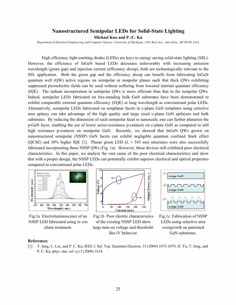
quantum effiche nonpolar n demonstrattional polar L
ates using seleepilayers andurther planarizs compared t
N QWs grownfined Stark e also succes
bited poor eleccteristics and d optical prop
brication of Ning selective awth on patternN substrates.
H. Yu, T. Jung
.
(SSL). mission
to the nGaN biting
ciency QWs. ted to LEDs. ective
d bulk ze the to still wn on effect
ssfully ctrical show
perties
NSSP area ned
g, and
26
Selective area epitaxy for GaN based optoelectronic devices and integration L. K. Lee and P.-C. Ku
Department of Electrical Engineering and Computer Science, University of Michigan, 1301 Beal Ave., Ann Arbor, MI 48109, USA.
III-nitride semiconductor material possesses unique properties such as a wide range of emission
wavelengths, large exciton binding energy and long spin coherence. These properties make them particularly attractive for applications in nanophotonics, spintronics and quantum information processing. In these applications, it is crucial to control the size, shape, and arrangement of the III-nitride semiconductor. Selective area epitaxy (SAE) is capable of precisely defining the site and dimension of the epitaxial materials, but its application to III-nitride semiconductors has been limited primarily to the defect reduction of GaN epitaxy on sapphire substrates. In this study, we exploit the SAE technique in MOCVD for III-nitride based optoelectronic devices. We believe the SAE technique will enable a more efficient integration of III-nitride devices and the production of site- and dimension-controlled III-nitride nanostructures.
27
Single-molecular sensing using the zeroth-mode optical waveguide L. K. Lee and P.-C. Ku
Department of Electrical Engineering and Computer Science, University of Michigan, 1301 Beal Ave., Ann Arbor, MI 48109, USA.
Ultrahigh sensitivity optical biosensing is critically needed for DNA sequencing, drug discovery,
and early disease detection. For example, real-time DNA sequencing has been recently demonstrated using the zeroth-mode waveguide. In this study, a large array of nanoscale metallic apertures was used to confine the excitation laser energy to a volume much beyond what can be achieved in conventional diffractive optics, e.g. confocal microscopy. Highly confined laser energy allows one to lower the required sample concentration while increasing the signal-to-noise ratio. Currently, the zeroth-mode waveguide was fabricated by electron-beam lithography. Hence the array size and therefore the throughput is considerably limited. In this study, we investigate novel nanofabrication techniques that can overcome this limit, potentially allowing one to perform large scale DNA sequencing and extend this technique to drug discovery and early disease detection. Experimental results will be presented at the Symposium.
28
High-Strength Electrically Conductive Fibers and Yarns for OLED-based Solid-State Lighting
Steven Morris1 Max Shtein2 1Chemical Engineering 2Materials Science and Engineering
University of Michigan, Ann Arbor, MI 48109
Electronic textiles (e.g. solar or lighting curtains, woven antennas, electronic clothing, and energy
harvesting structural fiber composites) is an emerging research area, focusing on devices that potentially combine the processing advantages of textile manufacturing with additional functionality that enables cloth- or structure-integrated communications, energy conversion, and computing capabilities. In the area of lighting in particular, we have shown1 5 cm-long fiber-based OLEDs that potentially can be scaled up to much larger lengths and enable cost-effective, high quality, high-efficiency solid-state lighting. However, the challenge of scaling up and structurally integrating fiber-based OLEDs is considerable, depending to a large extent on the availability of high strength, light-weight, and highly conductive substrates.
In this work, we demonstrate metal-coated, high-strength monofilament fibers and multifilament
yarns, achieving unprecedented combinations of specific strength and conductance. A combination of vacuum thermal evaporation, electroless deposition, and electroplating are used to produce these substrates, which include, for example, copper and nickel coated Kevlar yarns.
Mechanical and electrical tests of multi-filament conductive yarns reveal that twisted yarns have lower electrical resistance and higher strength, due to mitigation of cracks in the coating of the individual filaments and mutual bracing of the fibers. The greater surface area of yarns also allows for thinner conductive films, which reduces the probability of film delamination, compared with that for thicker films required for monofilament fibers. Performance and reliability characteristics of the coated fibers and yarns are mapped through tensile strength and conductance measurements performed under uniaxial stresses. Scanning electron microscopy is used to assess film quality and wear mechanisms, through observation of variations in grain structure, thickness, and film discontinuities. Theoretical models are utilized to compare experimental results to ideal fiber composites and to suggest methods for performance and reliability improvement. Specifically, using optimized metal coating techniques, we demonstrate a high tensile strength composite offering resistance less than 0.1 Ω/inch, well-suited to function as a robust substrate and bus line for OLEDs, enabling the possibility of strong, deployable OLED fabrics. 1. O’Connor, B. et al., “Fiber Shaped Light Emitting Device,” Advanced Materials, vol. 19, Nov. 2007,
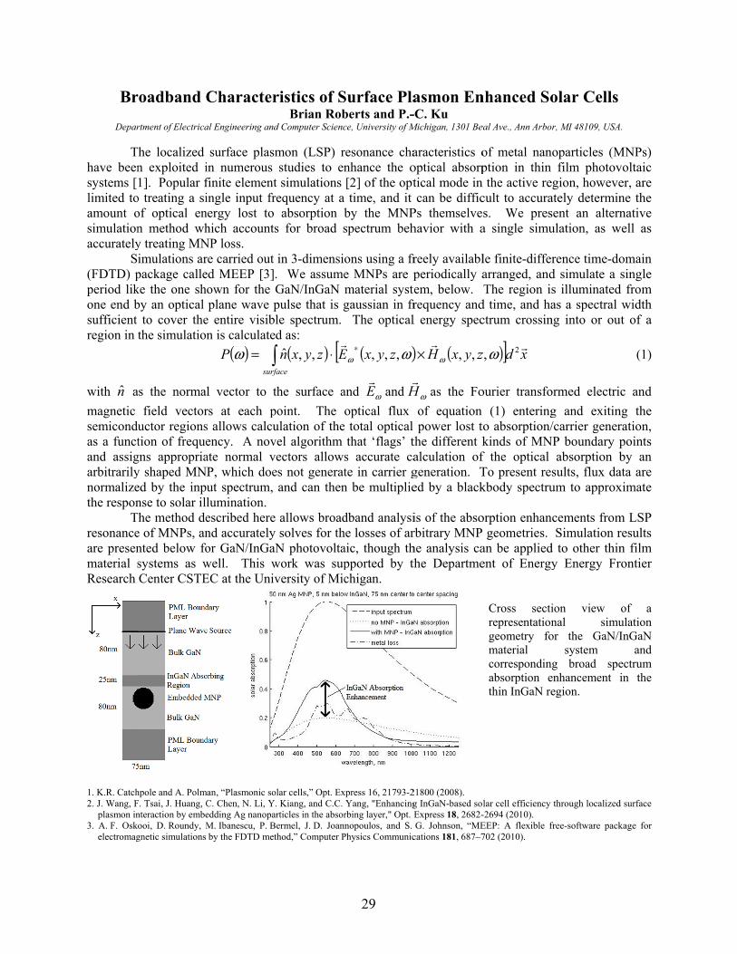
NP loss. re carried out ed MEEP [3].own for the Gplane wave p
e entire visibln is calculate
( )Psurf
ω = ∫l vector to trs at each ps allows calcuency. A novate normal vP, which doeut spectrum, lumination. escribed here nd accurately or GaN/InGaNwell. This wEC at the Univ
man, “Plasmonic soC. Chen, N. Li, Y.edding Ag nanopaM. Ibanescu, P. Bby the FDTD met
ristics of SBrian Rob
d Computer Scienc
mon (LSP) rstudies to en
t simulations requency at a
absorption bs for broad s
in 3-dimensio. We assumeGaN/InGaN mpulse that is gle spectrum. d as:
( ) [Ezyxnface
,,ˆ ⋅∫the surface apoint. The oulation of thevel algorithm ectors allows
es not generatand can then
allows broadsolves for th
N photovoltawork was supversity of Mic
olar cells,” Opt. Ex. Kiang, and C.C. rticles in the absorermel, J. D. Joannthod,” Computer P
29
Surface Plaberts and P.-ce, University of M
resonance chanhance the o[2] of the opttime, and it
by the MNPspectrum beh
ons using a fre MNPs are pmaterial systgaussian in fr The optical
( )zyxE ,,, ωω∗
and ωE and Hoptical flux total optical that ‘flags’ ts accurate cate in carrier gn be multiplie
dband analysihe losses of araic, though thpported by thchigan.
xpress 16, 21793-2Yang, "Enhancingrbing layer," Opt. Enopoulos, and S.
Physics Communic
asmon En-C. Ku Michigan, 1301 Be
aracteristics ooptical absorptical mode incan be diffic
Ps themselvehavior with a
freely availablperiodically a
tem, below. frequency andl energy spec
) ( zyxH ,,ω×
ωH as the Foof equation
power lost tthe different kalculation ofgeneration. Ted by a black
is of the absorbitrary MNPhe analysis cathe Departme
21800 (2008). g InGaN-based soExpress 18, 2682-G. Johnson, “ME
cations 181, 687–7
nhanced Soeal Ave., Ann Arbo
of metal nanption in thin
n the active recult to accuras. We presa single simu
le finite-diffearranged, andThe region is
d time, and hactrum crossin
)] xdz 2,ω
ourier transfo(1) entering
to absorption/kinds of MNf the optical To present rekbody spectru
orption enhan geometries.
an be appliedent of Energy
Cross sectirepresentationgeometry fomaterial correspondinabsorption ethin InGaN re
lar cell efficiency -2694 (2010). EEP: A flexible f702 (2010).
olar Cellsr, MI 48109, USA
noparticles (Mfilm photov
egion, howeveately determinsent an alternulation, as w
rence time-dod simulate a ss illuminatedas a spectral
ng into or ou
ormed electricg and exitin/carrier gener
NP boundary pabsorption b
sults, flux daum to approx
ncements from Simulation r
d to other thiny Energy Fr
ion view nal simuor the GaN/I
system ng broad speenhancement iegion.
through localized
free-software pack
.
MNPs) voltaic er, are ne the native
well as
omain single
d from width
ut of a
(1)
c and ng the ration, points by an
ata are ximate
m LSP results n film rontier
of a ulation InGaN
and ectrum in the
d surface
kage for
30
Study of CV Characteristics of ALD High-K dielectric ZnO Capacitors Jeffrey Siddiqui, Du Nguyen, Jamie Phillips, Kevin Leedy, Burhan Bayraktaroglu
Department of Electrical Engineering and Computer Science, University of Michigan, 1301 Beal Ave., Ann Arbor, MI 48109, USA.
ZnO Thin Film Transistors (TFTs) have attracted attention due to high carrier mobility in the
material. Many possible applications including low cost and/or flexible electronics exist. Recent results on these devices include the demonstration of high-performance operation at microwave frequencies [1]. The incorporation of high-k dielectrics is expected to further improve device performance, but there are few reports of the detailed electronic characteristics of ZnO/high-k dielectric interfaces. In this work, the characteristics of ZnO heterojunctions with high-k Al2O3 and HfO2 dielectrics deposited by atomic layer deposition will be presented with emphasis on capacitance-voltage characteristics of metal-dielectric-ZnO (MIS) structures. Materials consist of thin films including Al2O3 and HfO2 deposited by Atomic-Layer-Deposition and ZnO thin films deposited by Pulsed-Laser-Deposition. The metal-dielectric-metal capacitors indicate that Al2O3 and HfO2 have dielectric constants of approximately 10ε0 and 20ε0 and leakage currents of less than 2x10⁻⁹ and 2x10⁻⁷ A/cm2, respectively. Both films have breakdown fields of approximately 3x10⁶ V/cm. Capacitance-voltage characteristics of MIS structures show clear accumulation and depletion behavior with varying turn-on voltage of less than 1 V for Al2O3 dielectrics and more than 2 V for HfO2 dielectrics. Hysteresis is also seen with respect to voltage sweep directionality of 0.15V and 1.2V for Al2O3 and HfO2 respectively. Results summarized above and proposed future work will be presented in the poster. [1] B. Bayraktaroglu, K. Leedy, R. Neidhard, “Microwave ZnO Thin Film Transistors,” IEEE Elec. Dev. Lett., vol. 29. No. 9, Sep. 2008.
31
New Designs for LWIR/VLWIR FPI Michael Tulman
University of Michigan, Ann Arbor, MI 48109
Recently, the well-researched area of interferometry has undergone a transformation into MEMS. Whereas a Fabry-Perot interferometer (FPI) used to be the size of a desktop, they are now designed to fit on a semiconductor chip. The advantages to a smaller, more mobile FPI are numerous, especially for the military, and NASA. Up until now, most of the MEMS FPI have had very specific designs: they use a distributed Bragg reflector (DBR) design, and they’re tuned to the visible spectrum and near-infrared. Our objectives were twofold: to design an alternative to a DBR and to tune it to the LWIR/VLWIR This research has focused on the sub-wavelength reflector design. Sub-wavelength grating (SWG) is a series of dielectric gratings whose period is smaller than the half-wavelength of the spectrum over which it functions. The SWG design has many advantages over that of a DBR. Because the grating period must be on the scale of microns (and again, smaller than half-wavelength), it’s already on a scale of microns and therefore lends itself to a MEMS design. Also, to adjust the range of a DBR, one has to find the right combination of materials such that the reflectivity of the mirrors is optimized while not compromising structural integrity of the FPI. The SWG design is quite structurally sound, as it’s relatively thick. It’s a dielectric grating on top of a slab of lower-index material on top of a substrate. Secondly, the SWG design is broadband. The pass band for a DBR is 3%<Δλ/λ<9%. An SWG design can achieve a pass band Δλ/λ > 30%, it simply depends of the ratio of the indices of refraction of the grating and lower-index material. (The greater the ratio, the larger the pass band.) Thirdly, the DBR is designed in such a way that it is high loss, and low reflectivity. On the other hand, SWG FPI can achieve up to 99% reflectivity. Lastly, the SWG design can be scaled, in that you can scale the geometrical parameters by a factor to shift the spectrum the design reflects. To find an optimized geometry, simulations were designed using COMSOL, a multi-physics package that works with MATLAB. It was able to simulate the desired infrared spectrum hitting a SWG reflector with variable geometry (grating period, grating thickness, low-index material thickness, fill factor) and fixed indices of refraction for the grating and low-index material. The results obtained gave us a pass band of Δλ/λ > 42%, which went from 8-14 microns and was centered on 11 microns. The design also had a tolerance; many of the parameters could be slightly varied and still perform to the same specifications. So errors in fabrication would be tolerable. The SWG design is therefore a suitable alternative to the DBR, especially for the LWIR/VLWIR. The next step in this project is another alternative design, the lamellar grating design.
32
Microbial Nanowire Electronic Structure Probed by STM Joshua P. Veazey, Sanela Lampa-Pastirk, Gemma Reguera, and Stuart H. Tessmer
Michigan State University, East Lansing, MI.
We have studied the pilus nanowires expressed by the bacterium, Geobacter sulfurreducens, using high resolution scanning tunneling microscopy (STM). G. sulfurreducens is a metal reducing bacterium that has evolved electrically conductive type IV pili to efficiently transfer electrons outside the cell to, we believe, relatively remote distances. Here we employ the electronic sensitivity of STM to resolve the molecular substructure and the local density of states along the nanowire, in an effort to elucidate the mechanism of conduction. We observe tunneling spectra dependent upon the tip position that is consistent with complimentary voltage dependent topography.
33
Directed Matrix Seeding of Nitride Semiconductor Nanocrystals Adam W. Wood,1 Rachel R. Collino,2 Ben L. Cardozo,2 Y.Q. Wang,3 and Rachel S. Goldman1,2
1Department of Physics 2Materials Science and Engineering University of Michigan- Ann Arbor, MI 48109
3Materials Science and Technology Division Los Alamos National Lab Los Alamos, NM 87545
The controlled formation of semiconductor nanocomposites offers a unique opportunity to tailor
functional materials with a variety of novel properties. A promising approach to nanocomposite synthesis is matrix-seeded growth, which involves ion-beam-amorphization of a semiconductor film, followed by nanoscale re-crystallization via annealing [1,2]. In this work, we are studying the formation and evolution of N ion-implanted InAs and GaAs (InAs:N, GaAs:N). The InAs:N and GaAs:N nanocomposites are synthesized using 100keV ion-implantation with a dose of 5x1017cm-2, at 77K and 300C, respectively. In all cases, the as-implanted structures are primarily amorphous, and after appropriate rapid thermal annealing (RTA) sequences, zincblende (ZB) InN and GaN nanocrystals are formed [3,4]. In both cases, there is a transition to the wurtzite (WZ) phase with longer anneal times or higher temperatures. We are also developing a novel approach to direct the seeding of nanostructure arrays, using focused-ion-beam (FIB) implantation in combination with conventional ion implantation [5]. To date, we have demonstrated the selective positioning of WZ and ZB GaN nanocrystals using 75keV and 100keV N implantation, followed by FIB patterning and 800C RTA. The growth mechanisms and structural evolution of nitride crystallites will also be discussed. [1] X. Weng, S.J. Clarke, S. Kumar, R.S. Goldman, A. Daniel, R. Clarke, J. Holt, J. Sipowska, A. Francis, and V. Rotberg, J. Appl. Phys. 92 4012 (2002) [2] X. Weng, W. Ye, S.J. Clarke, R.S. Goldman, V. Rotberg, A. Daniel, and R. Clarke, J. Appl. Phys. 97 064301 (2005) [3] A.W. Wood, X. Weng, Y.Q. Wang, and R.S. Goldman, in preparation. [4] A.W. Wood, X. Weng, P.T. Wang, Y.Q. Wang, and R.S. Goldman, in preparation. [5] A.W. Wood, R.R. Collino, B.L. Cardozo, Y.Q. Wang, and R.S. Goldman, in preparation.
34
One-Step Direct Transfer of Pristine Single-Walled Carbon Nanotubes for Functional Nanoelectronics
Chung Chiang Wu, Chang Hua Liu, and Zhaohui Zhong* Department of Electrical Engineering and Computer Science, University of Michigan, Ann Arbor, MI 48109
We report a one-step direct transfer technique for the fabrication of functional nanoelectronic devices using pristine single-walled carbon nanotubes (SWNTs). Suspended SWNTs grown by the chemical vapor deposition (CVD) method are aligned and directly transferred onto pre-patterned device electrodes at ambient temperature. Using this technique, we successfully fabricated SWNT electromechanical resonators with gate-tunable resonance frequencies. Fully suspended SWNT p-n diode has also been demonstrated with diode’s ideality factor equal to 1. Our method eliminates the organic residues on SWNTs resulting from conventional lithography and solution processing. The results open up opportunities for the fundamental study of electron transport physics in ultraclean SWNTs, and for room temperature fabrication of novel functional devices based on pristine SWNTs.
35
Graphenen Nanoribbons Produced from Sonicating Graphite in Solution for Device Applications
Cheng Ling1, Gabriel Setzler1,2, Jin Jin1, Ming-Wei Lin1, Hyeun Joong Yoon2, Seung Soo Kim1,2, Jinho Yang2, Xuebing Tan2, Yiyang Zhang2, Mark Ming-Cheng Cheng2 and Zhixian Zhou1, *
1Department of Physics and Astronomy, Wayne State University, Detroit, MI 48201 2Department of Electrical and Computer Engineering, Wayne State University, Detroit, MI 48202
A simple one-stage solution-based method was developed to produce graphene nanoribbons by
sonicating graphite powder in organic solutions with polymer surfactant. Graphene nanoribbons were deposited on silicon substrate with thermal oxide, and characterized by non-contact mode atomic force microscopy. Single layer and few layer graphene nanoribbons with width ranging from sub-10 nm to tens of nm and length ranging from hundreds of nm to 1 µm were routinely observed. Electrical transport measurements on field effect transistors consisting of individual graphene nanoribbons showed ambipolar transfer characteristics that are typical for graphene field effect transistors. A mobility of approximately 200 cm2/ V s was estimated, indicating the presence of a small amount of disorder. i R. R. Collino, B. B. Dick, F. Naab, Y. Q. Wang, M. D. Thouless, and R. S. Goldman, Appl. Phys. Lett. 95, 111912 (2009). ii E. Jalaguier et al., Electron. Lett. 34, 408 (1998).