Wideband active microwave isolators using GaAs MMIC technology D.G. Haigh Indexing terms: Wideband microwave isolators, GaAs M M C technology, Monolithic microwave integrated circuit Abstract: The paper is concerned with circuit designs for wideband microwave isolators realised as monolithic microwave integrated circuits using depletion-mode GaAs MESFETs. An unbalanced version of a previously published balanced design is shown to have an interesting property of an approximately linear transmission function but the port impedances remain nonlinear. A previously published general circuit synthesis method is used to implement an isolator with transmission function and port impedances both of which are linearised. Measurements on a GaAs MMIC implementation are presented. 1 introduction Many system functions realised by traditional micro- wave technologies are now being implemented using GaAs monolithic microwave integrated circuit (MMIC) design techniques [ 11. The isolator, which is tradition- ally realised passively using ferrite [2], is a key compo- nent in many microwave systems for preventing unwanted interactions between components. An active MMIC implementation of the isolator function, in order to reduce cost, size and weight, has been pro- posed [3]. The circuit consists essentially of a balanced structure where each path consists of a parallel-parallel interconnection of a common-gate and a common- drain GaAs MESFET. We begin by investigating the nonlinearity of the basic isolator configuration of a parallelled common- gate and common-drain FET and show that it pos- sesses a transmission function which is approximately linear inspite of the nonlinearity of the FETs used. However, the input and output impedances depend directly on the nonlinearity of the FET and are there- fore nonlinear. Next, the general FET circuit synthesis technique in [4-61 is used to synthesise an isolator which is linearised both in respect of its input and out- put impedances and its transmission function. Finally, the design of a GaAs MMIC realisation is discussed and measurement results are presented. 0 IEE, 1996 IEE Proceedings online no. 19960226 Paper first received 11th August 1995 and in revised form 8th November 1995 The author is with the Department of Electronic and Electrical Engineer- ing, University College London WClE 7JE, UK 2 Active isolator implementation The isolator is a two-port network required to have a forward gain of unity, reverse gain of zero and perfect matching at both ports, or, in terms of S and Y param- eters, L A .;-[ Go 01 -2Go Go where Go is 20mS assuming a 50Q system. We now consider implementation of eqn. 1 using FETs. As a very simple second-order approximation, FETs can be described by Pa) I, = -Id (2b) Ig = 0 (24 2 Id = P(vgs - VT) where Id, I, and Ig are drain, source and gate current, Vggs is gate-source voltage, p and V, are constants and operation at frequencies well below the device fT is assumed. For the purpose of carrying out a small-sig- nal design, we may linearise eqn. 2 and represent the FET by the indefinite admittance matrix [7] 0 0 0 wg [ = [ : I Gm :] [ *:1 (3) -Grn where G, is small-signal transconductance (= id/lvg, = dId/dVg,). From eqn. 3, the admittance matrix of the common-gate FET is obtained by deleting the first row and column and the admittance matrix of the common- drain FET is obtained by deleting the third row and column [7] Hence, we see that the isolator admittance matrix in eqn. lb may be realised as in [3] by a parallel connec- tion of a common-gate and common-drain FET where for both FETs G, = Go. In general a circuit designed using the linearised FET description as in eqn. 3 will have an unpredictable nonlinear perfonnance because the nonlinear part of the FET description has been ignored. 179 IEE Proc.-Microw. Antennas Propug., Vol. 143, No. 2, April 1996
Transcript
Wideband active microwave isolators using GaAs MMIC technology
D.G. Haigh
Indexing terms: Wideband microwave isolators, GaAs M M C technology, Monolithic microwave integrated circuit
Abstract: The paper is concerned with circuit designs for wideband microwave isolators realised as monolithic microwave integrated circuits using depletion-mode GaAs MESFETs. An unbalanced version of a previously published balanced design is shown to have an interesting property of an approximately linear transmission function but the port impedances remain nonlinear. A previously published general circuit synthesis method is used to implement an isolator with transmission function and port impedances both of which are linearised. Measurements on a GaAs MMIC implementation are presented.
1 introduction
Many system functions realised by traditional micro- wave technologies are now being implemented using GaAs monolithic microwave integrated circuit (MMIC) design techniques [ 11. The isolator, which is tradition- ally realised passively using ferrite [2], is a key compo- nent in many microwave systems for preventing unwanted interactions between components. An active MMIC implementation of the isolator function, in order to reduce cost, size and weight, has been pro- posed [ 3 ] . The circuit consists essentially of a balanced structure where each path consists of a parallel-parallel interconnection of a common-gate and a common- drain GaAs MESFET.
We begin by investigating the nonlinearity of the basic isolator configuration of a parallelled common- gate and common-drain FET and show that it pos- sesses a transmission function which is approximately linear inspite of the nonlinearity of the FETs used. However, the input and output impedances depend directly on the nonlinearity of the FET and are there- fore nonlinear. Next, the general FET circuit synthesis technique in [4-61 is used to synthesise an isolator which is linearised both in respect of its input and out- put impedances and its transmission function. Finally, the design of a GaAs MMIC realisation is discussed and measurement results are presented. 0 IEE, 1996 IEE Proceedings online no. 19960226 Paper first received 11th August 1995 and in revised form 8th November 1995 The author is with the Department of Electronic and Electrical Engineer- ing, University College London WClE 7JE, UK
2 Active isolator implementation
The isolator is a two-port network required to have a forward gain of unity, reverse gain of zero and perfect matching at both ports, or, in terms of S and Y param- eters,
L A .;-[ Go 0 1 -2Go Go
where Go is 20mS assuming a 50Q system. We now consider implementation of eqn. 1 using FETs. As a very simple second-order approximation, FETs can be described by
P a )
I , = - I d ( 2b ) Ig = 0 ( 2 4
2 I d = P ( v g s - VT)
where Id, I, and Ig are drain, source and gate current, Vggs is gate-source voltage, p and V, are constants and operation at frequencies well below the device f T is assumed. For the purpose of carrying out a small-sig- nal design, we may linearise eqn. 2 and represent the FET by the indefinite admittance matrix [7]
0 0 0 wg
[ = [:I Gm :] [ *:1 (3)
-Grn where G, is small-signal transconductance (= id/lvg, = dId/dVg,). From eqn. 3 , the admittance matrix of the common-gate FET is obtained by deleting the first row and column and the admittance matrix of the common- drain FET is obtained by deleting the third row and column [7]
Hence, we see that the isolator admittance matrix in eqn. lb may be realised as in [3] by a parallel connec- tion of a common-gate and common-drain FET where for both FETs G, = Go. In general a circuit designed using the linearised FET description as in eqn. 3 will have an unpredictable nonlinear perfonnance because the nonlinear part of the FET description has been ignored.
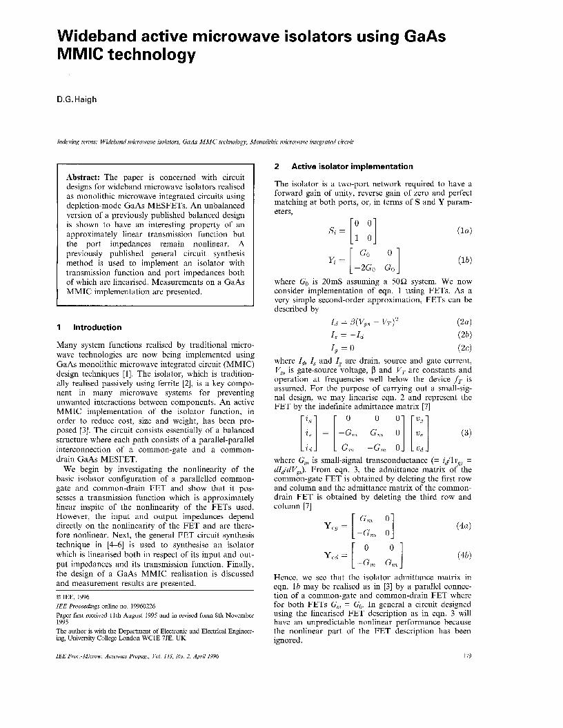
An isolator consisting of the parallel connection of a common-drain FET MA and a commongate FET MB is shown without bias circuits in Fig. 1. We assume that the FETs are described by the simple model of eqn. 2 and that the FETs are biased at Vgs = OV. Mc has its gate-source port shorted and realises a constant current source for biasing. We assume that the terminating conductances Go match the small-signal input conduct- ance of the common-gate FET and the output conduct- ance of the common-drain FET both of which are given by Go = -2pVF For the isolator itself (i.e. ignor- ing the terminating conductances Go), the nonlinear port description in admittance form [8] may be shown to be [;I = - 2 m [ O][vl] + P [ -Vf ] ( 5 )
-2 1 v, - vz" + 2v, v, where I,' and I,' are defined in Fig. 1. The first term in eqn. 5 contains the isolator small-signal admittance matrix (eqn. lb) and the second term describes its non- linear behaviour. The circuit is intended to be operated with a 50Q load at port 2 (Go) and a 5052 voltage source at port 1 (V,, Go; see inset in Fig. 1) where Go = -2pVT. The 50R voltage source may be replaced by its Norton equivalent (Is, Go) as shown in Fig. 1.
Fig. 1 Simple isolator circuit based on [3]
The two port network comprising the terminating conductances Go which has admittance matrix descrip- tion
is connected in parallel-parallel with the isolator. Hence, the admittance terms in eqn. 6 may be added to those in eqn. 5 to yield the description for the isolator plus terminating conductances [;I = - 2 m [ "I["] + B [ -V,z ] (7)
-2 2 v, -vz" + 2v,v, The output current I2 may be set to zero, and, since the second row of eqn. 7 is linear in V I , we may eliminate VI in the first row to obtain a relationship between I , and a nonlinear function of the output voltage V2. Finally, the input current I , (= I,) may be replaced by its Thevenin equivalent (VsGO), where V, is the source voltage, to obtain
180
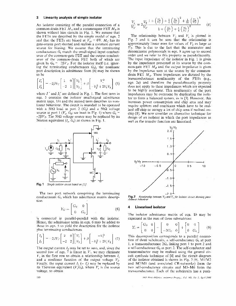
The relationship between V2 and V, is plotted in Fig. 2 and it can be seen that the relationship is approximately linear even for values of V, as large as V,. This is due to the fact that the numerator and denominator polynomials in eqn. 8 agree up to second order and we refer to this property as pseudolinearity. The input impedance of the isolator in Fig. 1 is given by the impedance presented at its source by the com- mon-gate FET MB and the output impedance is given by the impedance seen at the source by the common- drain FET MA. These impedances are dictated by the transconductance nonlinearity of the FETs (e.g., eqn. 2a) and therefore the pseudolinearity property does not apply to these impedances which are expected to be highly nonlinear. This nonlinearity of the port impedances may be overcome by duplicating the isola- tor to form a balanced system, as in [3]. However, this increases power consumption and chip area and may require splitters and combiners which have to be real- ised off-chip or occupy a lot of chip area if realised on- chip [l]. We now consider an alternative technique for design of an isolator in which the port impedances as well as the transfer function are linearised.
- 2 0 1 Fi .2 dokeav behaviour
Relationship between V, and V, for isolator circuit showing pseu-
4 Linearised isolator
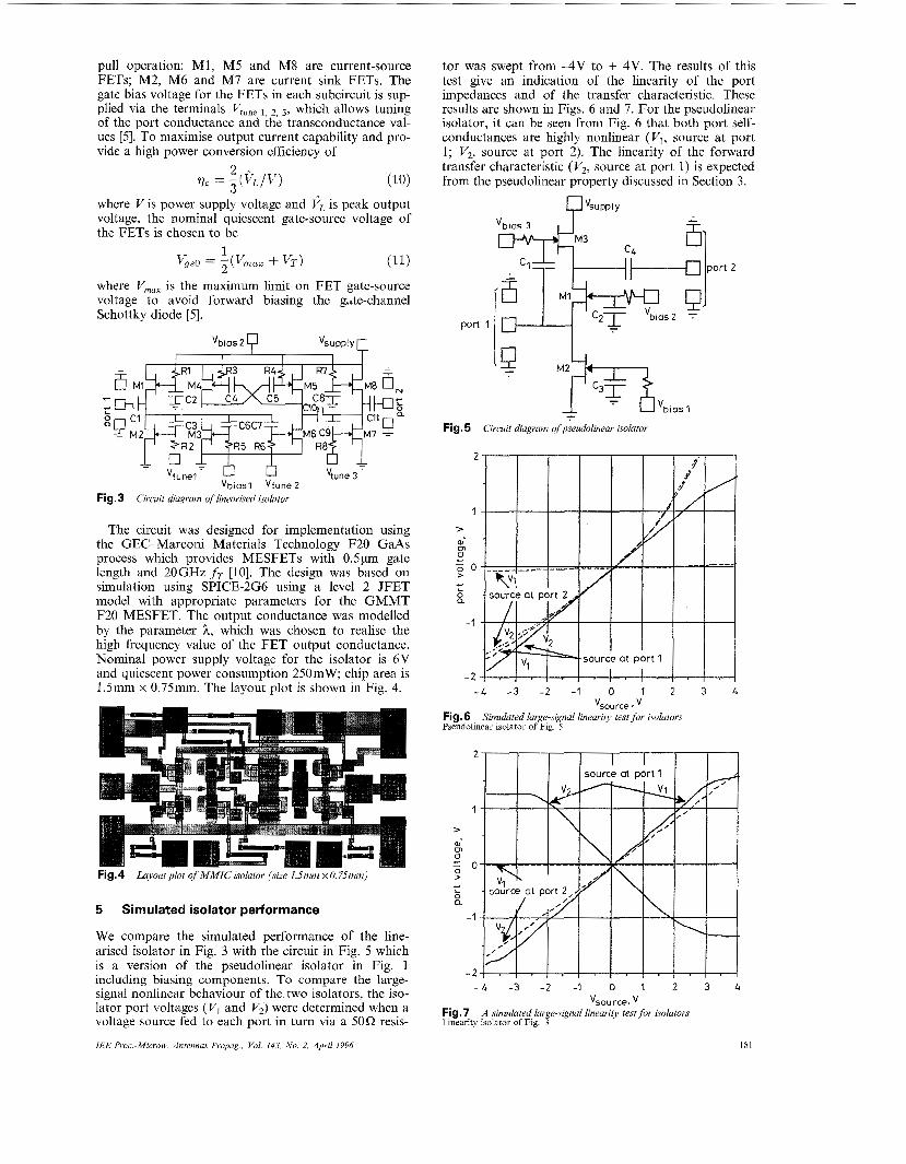
The isolator admittance matrix of eqn. 16 may be expressed as the sum of three submatrices:
This decomposition corresponds to a parallel connec- tion of three subcircuits, a self-conductance Go at port 1, a transconductance 2G0 linking port 1 to port 2 and a self-conductance Go at port 2. The self-conductor and transconductor may be realised using the general cir- cuit synthesis technique of [4] and the circuit diagram of the isolator obtained is shown in Fig. 3 [9]. MUM2 and M7/M8 (and associated CR-networks) form the two self-conductance circuits and M3-M6 form the transconductance. Each of the subcircuits has a push-
IEE Pvoc -Mccrow Antennas Propag , Vol 143 No 2, April 1996
pull operation: M1, M5 and M8 are current-source FETs; M2, M6 and M7 are current sink FETs. The gate bias voltage for the FETs in each subcircuit is sup- plied via the terminals VtUne 2, 3, which allows tuning of the port conductance and the transconductance val- ues [5]. To maximise output current capability and pro- vide a high power conversion efficiency of
(10) 2
rlc = p / v )
v g s o = ~(vmaz + VT)
where Vis power supply voltage and VL is peak output voltage, the nominal quiescent gate-source voltage of the FETs is chosen to be
(11) 1
where V,,, is the maximum limit on FET gate-source voltage to avoid forward biasing the gkte-channel Schottky diode [5].
I I I
‘bias 2 7
‘tune1 ‘tune 3 ‘bias1 ‘tune 2
Fig. 3 Circuit diagram of linearised isolator
The circuit was designed for implementation using the GEC-Marconi Materials Technology F20 GaAs process which provides MESFETs with 0 . 5 ~ gate length and 20GHz f’ [lo]. The design was based on simulation using SPICE-2G6 using a level 2 JFET model with appropriate parameters for the GMMT F20 MESFET. The output conductance was modelled by the parameter h, which was chosen to realise the high frequency value of the FET output conductance. Nominal power supply voltage for the isolator is 6V and quiescent power consumption 250mW; chip area is 1.5mm x 0.75mm. The layout plot is shown in Fig. 4.
Fig.4 Layout plot of MMIC isolator (size 1.5mm x 0.75mm)
5 Simulated isolator performance
We compare the simulated performance of the line- arised isolator in Fig. 3 with the circuit in Fig. 5 which is a version of the pseudolinear isolator in Fig. 1 including biasing components. To compare the large- signal nonlinear behaviour of the two isolators, the iso- lator port voltages (Vl and V,) were determined when a voltage source fed to each port in turn via a 50Q resis-
IEE Proc -Microw Antennay Piopag , Vol 143, No 2, April I996
tor was swept from -4V to + 4V. The results of this test give an indication of the linearity of the port impedances and of the transfer characteristic. These results are shown in Figs. 6 and 7. For the pseudolinear isolator, it can be seen from Fig. 6 that both port self- conductances are highly nonlinear (VI, source at port 1; V,, source at port 2). The linearity of the forward transfer characteristic (V,, source at port 1) is expected from the pseudolinear property discussed in Section 3.
PJ 2 7
Fig. 5 Circuit diagram of pseudolinear isolator
- 4 -3 -2 -1 0 1 2 3 4 ‘sou rce ’ “
Fig. 6 Pseudolinear isolator of Fig. 5
Simulated large-signal linearity test for isolators
2
1
> a; cn 0 L
z o d
s a -1
-2 - 4 -3 -2 -1 0 I 2 3 4
‘source. V Fig. 7 Linearity isolator of Flg. 3
A simulated large-signal linearity test for isolators
181
For the linearised isolator, Fig. 7 shows excellent lin- earity of the self-conductance at both ports; linearity of the forward transfer characteristic is reasonable and can be improved by optimum choice of power supply voltage and biasing in relation to FET parameters; these factors are more critical for a linearised circuit. Comparison of Figs. 6 and 7 show that, for large sig- nals, isolation (VI, source at port 2) is substantially bet- ter for the linearised isolator, which is expected because the design of the linearised isolator takes large signal conditions into account.
0
-1 0
-20 m U
-x -30
!E x
-4 0
-50
- 60
108 1 o9 frequency, GHz
Fig. 8 , Simulated S-parameters against frequency for isolators Pseudolinear isolator of Fig. 5
108 109 frequency, H
Fig. 9 Linearised isolator of Fig. 3
Simulated S-parameters against frequency for isolators
The curves in Figs. 8 and 9 show small-signal S- parameters as a function of frequency. Considerably superior isolation for the linearised isolator (Fig. 9) can be observed but there is some reduction in bandwidth due to the loading of the input port by the input capac- itance of the transconductance stage. Deterioration in S2, at low frequencies in Fig. 8 and of Sll and S2, at low frequencies in Fig. 9 is due to coupling capacitors included in the designs (C, and Cll in Fig. 3; C, in Fig. 5); these coupling capacitors are not required if balanced power supplies are used and will be omitted in future designs. Such an approach is expected to lead to curves similar to SI1 in Fig. 8 in all cases.
182
6 Experimental results
The linearised isolator was fabricated using the GEC- Marconi Materials Technology F20 GaAs process. The linearised isolator chip was bonded onto a ceramic car- rier which interfaced with a test jig and an HP 8510 network analyser. The measured DC supply current was 40mA with a nominal power supply voltage of 6V. The nominal test signal level was OdBm.
1 1 1
1 Fig. 10 Horizontal scale 0 5 to 5 5GHz Vertical scale +5 to 4 5 d B
Measured S-parameters for MMIC isolator
The measured magnitudes of the S-parameters against frequency of the circuit for nominal power sup- ply voltage and input signal level are shown in Fig. 10. The curves are similar to the simulated curves in Fig. 9. The SI, reverse isolation values follow the simulations in Fig. 9 with good accuracy maintaining figures of - 40dB at lGHz and -30dB at 3GHz. The -3dB band- width estimated from the S2, curve is about 8.6GHz. The circuit is thus shown to perform reasonably well with negligible effect from the bond wires linking the chip to the substrate. It was necessary to carry out some tuning of the low frequency response and this suggests that the design is not optimally centred. This is expected from the relatively simple device model used in the design.
Fig. 11 Horizontal scale: 0.5 to 5.5GHz
Measured Szr for MMIC isolator against input signal level
Vertical scale: +3 to -7dB
To evaluate the linearity of the circuit, the magnitude of the forward transfer function S2, was measured for a range of input signal levels from -10dBm to +20dBm. The results plotted with an expanded amplitude scale are shown in Fig. 11. It can be seen that the response is little affected by changes in signal level and that the spread in gain is only about 0.5dB.
IEE Proc -Micvow Antennas Propag , Vol 143, No 2, April 1996
The forward transfer function S2, was measured for a range of power supply voltage values from 3 to 8V and the results are shown plotted in Fig. 12 with an expanded amplitude scale. Even with a supply voltage of 3V, which corresponds to Vds of 1 . W for each FET, the shape of the curve is unaffected although there is a loss of about 1.5dB. For power supply voltages of between 4V and 8V, the spread in gain is less than 0.5dB. These results indicate a reasonably low sensitiv- ity of response to power supply voltage, even for large power supply voltage variations.
Fig. 12 Horizontal scale: 0.5 to 5.5GHz Vertical scale: + 3 to -7dB
Measured S,, for MMIC isolator against power supply voltage
E - 2 0 t
-3 0 % a; 3 -40
Q -50 ‘ -60 -70
-8 0
U = -
-90 -8.5 -6.5 -4.5 -2.5 -0.5 1.5 3.5 5.5 7.5
Pin. dBm Fi 13 Measured and simulated levels of undamental and seconathird or% intermodulation distortion for linearisedfisolator
~ measured _ _ _ _ simulated
Finally, the level of measured second and third order intermodulation distortion versus input signal level is shown in Fig. 13, together with simulations using SPICE3J2 with a Parker-Skellern model [ I l l for the GMMT F20 MESFET. The total difference frequency distortion technique [ 121 was used with input frequen- cies of 990MHz VI) and 1490MHz (f2); the second and third order intermodulation products were measured at 500MHz Vi -fl) and 490MHz (295 -f2), respectively. All of these frequencies lie in the passband of the isola- tor. Despite the fact that the linearisation technique on which the circuit is based must break down at high fre- quencies due to device-circuit interaction of the linear components of the FET gate-source and gate-drain capacitances [ 131, the distortion levels indicated in Fig. 13 are reasonably low. The second and third order input intermodulation intercept points are 30dBm and 20dBm, respectively.
IEE Proc.-Microw. Antennas Propag., Vol. 143, No. 2, April 1996
7 Conclusions
We have considered the realisation of wideband micro- wave isolators using depletion-mode GaAs MESFETs. We have shown that the simple isolator architecture consisting of the parallel connection of a common- drain and a common-gate FET has a transfer function which is approximately linear assuming a simple FET model. This property is referred to as pseudolinearity and it was observed that it does not apply to the isola- tor port self-conductances. We then considered an alternative isolator design based on use of linearised self-conductance and transconductance circuits devel- oped previously. Computer simulation of the pseudo- linear and linearised isolators confirmed the expected performance behaviour. Finally, we presented S- parameter and distortion measurements on the line- arised MMIC isolator chip which confirmed its opera- tion. Omission of the coupling capacitors from the design will improve matching and bandwidth and sig- nificantly reduce chip area. Higher frequency operation will be possible using faster IC processes such as the GEC Marconi Materials technology 40GHz fr HEMT process [IO].
8 Acknowledgments
The author would like to thank D. Dapra for carrying out distortion measurements and various colleagues for helping with different aspects of the work, including C. Losada and D. Webster of UCL, A. Parker of Mac- quarie University (Sydney), J. Scott of the University of Sydney and M. Darvishzadeh of EPSRC Rutherford Appleton Laboratory.
9
1
2
3
4
5
6
7
8
9
References
ROBERTSON, I.D. (Ed.): ‘MMIC design’ (IEE Books, London, 1995) HELSZAJN, J.: ‘Microwave planar passive circuits and filters’ (John Wiley & Sons, 1994) ALI, F., and PODELL, A.: ‘A wideband push-pull monolithic active isolator’, IEEE Microw. Guid. Wave Leti., 1991, 1, (2), pp. 2&27 HAIGH, D.G., and TOUMAZOU, C.: ‘Synthesis of transcon- ductorimultiplier circuits for GaAs technology’, IEEE Trans. Cir- cuits Syst., 1992, 39, (2), pp. 81-92 HAIGH, D.G., LOSADA, C.A., PARKER, A.E., and WEB- STER, D.R.: ‘Systematic approach for the development and design of analogue communication circuits’ in DEDIEU, H. (Ed.): ‘Selected topics in circuits and systems’ (Elsevier, Oxford,
HAIGH, D.G., and TOUMAZOU, C.: ‘Synthesis of linearised conductance functions’ in GOYAL, R. (Ed.): ‘High frequency analog integrated circuit desgin’ (John Wiley & Sons, 1995), Chap. 10, pp. 349-392 BALABANIAN, N., and BICKART, T.A.: ‘Electrical network theory’ (John Wiley & Sons, 1969) LOSADA, C.A., HAIGH, D.G., and RADMORE, P.M.: ‘A sys- tematic method for nonlinear analysis of a class of FET circuits’, IEEE international symposium on Circuits and systems, Chicago, 3-6 May 1993, pp. 2086-2089 HAIGH, D.G.: ‘Circuit techniques for efficient linearised GaAs MMICs’. IEEE international microwave svmuosium MTT-S.
1993), pp. 3-74
, 1
Albuquerque, 1-5 June 1992, pp. 1035-1038 10 EATON, R.M., and MYERS, F.A.: ‘Technology, Circuit design
and applications of GaAs MMICs’, Electron Commun. Eng. J., 1990, 2, (6), pp. 23343
11 PARKER, A.E.: ‘Implementing high-order continuity and rate- dependence in SPICE models’, IEE Proc. Circuits, Devices, Syst., 1994, 141, (4), pp. 251-257
12 PARKER, A.E., and SCOTT, J.B.: ‘Intermodulation nulling in GaAs MESFETs’, Electron. Lett., 1993, 29, (22), pp. 1961-1962
13 WEBSTER, D.R., HAIGH, D.G., and PARKER, A.E.: ‘Distor- tion compensation of multi-MESFET circuits’, IEEE interna- tional symposium on Circuits and systems, London, 30 May-2 June 1994, pp. 5/189-192