Wire Load Model for Rapid Power Consumption Evaluation in Early Design Stage of Via-Switch FPGA Asuka Natsuhara †1 Takashi Imagawa †2 Hiroyuki Ochi †1,2 †1 Graduate School of Information Science and Engineering, Ritsumeikan University †2 College of Information Science and Engineering, Ritsumeikan University 1-1-1 Noji-higashi, Kusatsu, Shiga, 525-8577 Japan [email protected], [email protected], [email protected]Abstract— This paper proposes a wire load model for via-switch FPGA to allow simulation-based power estimation before routing. Via-switch FPGA is ex- pected to achieve a dramatic improvement in the area, delay, and power compared with conventional SRAM-based FPGA. To estimate the power consump- tion of an application circuit mapped on a via-switch FPGA, time-consuming routing process was needed before circuit simulation. Using the proposed post- placement simulation flow, runtime for power estima- tion is reduced by 63.8% on average compared with the conventional post-routing simulation flow, with 11.8% degradation of estimation error on average. I. Introduction The recent progress of manufacturing processes im- proved the scale, performance, and energy efficiency of cir- cuits that application specific integrated circuits (ASICs) can realize. On the other hand, however, higher costs and longer time for development and fabrication of ASICs have become a serious problem. As an alternative for the ASICs, reconfigurable devices that allow the users to change the circuit configuration after fabrication are getting the attention. Among reconfigurable devices, FP- GAs that hold configuration information in SRAM cells (SRAM-type FPGAs) have made remarkable progress, thanks to advances in CMOS process technology. How- ever, SRAM-type FPGAs are far worse in area, delay, and power consumption than ASICs in exchange for their flex- ibility [1]. One of the factors is that the area of the SRAM cell used to hold configuration information is large. To reduce the area, power and performance overhead of conventional FPGAs, a new reconfigurable device has been proposed that realizes the ON/OFF switching func- tion between the wire segments by an element called an atom switch instead of an SRAM cell and a pass transis- tor [2]. Atom switch is a kind of a non-volatile resistive- change switch. It occupies a small footprint area and is integrated on back-end-of-line (BEoL) layers. In [3], not only the routing resources of FPGA but also the truth table of LUT (Look-Up Table) that serves as the logic resource is realized using atom switches. Refer- ence [4] proposes a 0-1-A- A LUT to further improve the area and delay of the LUT in [3]. Thanks to the fact that the atom switch has lower resistance and smaller parasitic capacitance than the pass transistor, one of the LUT input signals of the 0-1-A- A LUT is connected to the switch array, unlike conventional FPGAs in which all inputs are connected to the selection signals of the mul- tiplexer (MUX). Reduction of power consumption as well as area and delay has been confirmed for LUT alone [5]. However, it has not been evaluated how much 0-1-A- A LUT contributes to low power consumption by imple- menting benchmark circuits of practical size on an FPGA with a large number of LUTs. To evaluate the power con- sumption of the entire FPGA, it is necessary to analyze power consumption not only of LUTs but also of wire segments. To evaluate power consumption considering parasitic capacitance of wire segments, however, required time-consuming post-routing circuit simulation. To eliminate the routing process from power estima- tion, this paper proposes a wire load model for via-switch FPGA derived from actual placement and routing results of circuits and present the experimental results of power consumption analysis using the model. The standard de- viation of the relative estimation error on the number of switches calculated by the proposed post-placement model is 15.0% in the worst case, while that of the post-synthesis model is 46.6%. Using the proposed post- placement simulation flow, runtime for power estimation is reduced by 63.8% on average compared with the con- ventional post-routing simulation flow, with 11.8% degra- dation of estimation error on average. The next section reviews via-switch device and via- switch FPGA architecture, and power estimation method for conventional FPGAs. Section 3 proposes the wire load model that utilizes post-placement information, and Sec- tion 4 evaluates the accuracy and runtime of the proposed method. Section 5 concludes the paper. SASIMI 2019 Proceedings R4-11 - 298 -
Transcript
Wire Load Model for Rapid Power Consumption Evaluationin Early Design Stage of Via-Switch FPGA
†1 Graduate School of Information Science and Engineering, Ritsumeikan University†2 College of Information Science and Engineering, Ritsumeikan University
Abstract— This paper proposes a wire load modelfor via-switch FPGA to allow simulation-based powerestimation before routing. Via-switch FPGA is ex-pected to achieve a dramatic improvement in thearea, delay, and power compared with conventionalSRAM-based FPGA. To estimate the power consump-tion of an application circuit mapped on a via-switchFPGA, time-consuming routing process was neededbefore circuit simulation. Using the proposed post-placement simulation flow, runtime for power estima-tion is reduced by 63.8% on average compared withthe conventional post-routing simulation flow, with11.8% degradation of estimation error on average.
I. Introduction
The recent progress of manufacturing processes im-proved the scale, performance, and energy efficiency of cir-cuits that application specific integrated circuits (ASICs)can realize. On the other hand, however, higher costsand longer time for development and fabrication of ASICshave become a serious problem. As an alternative forthe ASICs, reconfigurable devices that allow the usersto change the circuit configuration after fabrication aregetting the attention. Among reconfigurable devices, FP-GAs that hold configuration information in SRAM cells(SRAM-type FPGAs) have made remarkable progress,thanks to advances in CMOS process technology. How-ever, SRAM-type FPGAs are far worse in area, delay, andpower consumption than ASICs in exchange for their flex-ibility [1]. One of the factors is that the area of the SRAMcell used to hold configuration information is large.
To reduce the area, power and performance overheadof conventional FPGAs, a new reconfigurable device hasbeen proposed that realizes the ON/OFF switching func-tion between the wire segments by an element called anatom switch instead of an SRAM cell and a pass transis-tor [2]. Atom switch is a kind of a non-volatile resistive-change switch. It occupies a small footprint area and isintegrated on back-end-of-line (BEoL) layers.
In [3], not only the routing resources of FPGA but also
the truth table of LUT (Look-Up Table) that serves asthe logic resource is realized using atom switches. Refer-ence [4] proposes a 0-1-A-A LUT to further improve thearea and delay of the LUT in [3]. Thanks to the factthat the atom switch has lower resistance and smallerparasitic capacitance than the pass transistor, one of theLUT input signals of the 0-1-A-A LUT is connected tothe switch array, unlike conventional FPGAs in which allinputs are connected to the selection signals of the mul-tiplexer (MUX). Reduction of power consumption as wellas area and delay has been confirmed for LUT alone [5].However, it has not been evaluated how much 0-1-A-ALUT contributes to low power consumption by imple-menting benchmark circuits of practical size on an FPGAwith a large number of LUTs. To evaluate the power con-sumption of the entire FPGA, it is necessary to analyzepower consumption not only of LUTs but also of wiresegments. To evaluate power consumption consideringparasitic capacitance of wire segments, however, requiredtime-consuming post-routing circuit simulation.
To eliminate the routing process from power estima-tion, this paper proposes a wire load model for via-switchFPGA derived from actual placement and routing resultsof circuits and present the experimental results of powerconsumption analysis using the model. The standard de-viation of the relative estimation error on the numberof switches calculated by the proposed post-placementmodel is 15.0% in the worst case, while that of thepost-synthesis model is 46.6%. Using the proposed post-placement simulation flow, runtime for power estimationis reduced by 63.8% on average compared with the con-ventional post-routing simulation flow, with 11.8% degra-dation of estimation error on average.
The next section reviews via-switch device and via-switch FPGA architecture, and power estimation methodfor conventional FPGAs. Section 3 proposes the wire loadmodel that utilizes post-placement information, and Sec-tion 4 evaluates the accuracy and runtime of the proposedmethod. Section 5 concludes the paper.
SASIMI 2019 ProceedingsR4-11
- 298 -
��
��
��
���
��
�
�������� �������
������
Fig. 1.: Atom switch.
����� �
���
��
�� ��
Fig. 2.: Via-switch.
���������
����� ��
������
�� ��
�� ����
�����������
��
�� ��
��
���������
����������
������
���������
����� ��
���������٠����
����٠�����
Fig. 3.: Equivalent circuit model of a via-switch [8].
II. Background
A. Atom switch
Atom switch is a nonvolatile switch device that uti-lizes formation of a copper bridge from metal ion and itsextinction [2]. It is composed of a solid-electrolyte sand-wiched between copper (Cu) and ruthenium (Ru) elec-trodes. By applying a positive voltage to the Cu elec-trode, a Cu bridge is formed in the solid-electrolyte, andthe switch turns ON. When a negative voltage is applied,the Cu atoms in the bridge are reverted to the Cu elec-trode, and the switch turns OFF. Figure 1 shows the ON-and OFF-state of the atom switch.
To improve the OFF-state reliability of the device,Complementary Atom Switch (CAS) that consists of twoatom switches connected in series with opposite direc-tion has been proposed [6]. Via-switch with two varistorsstacked on a CAS has also been proposed to allow writ-ing multi-fanout routing to two-dimensional CAS arraywithout using access transistors [7]. Figure 2 and 3 showsthe structure of the via-switch and its equivalent circuitmodel, respectively.
Since the via switch has both state storage and a switchfunction, it replaces the programmable switch elementused in the existing FPGA, that is, an SRAM cell for thestate storage and a pass transistor for the switch function.The via-switch is superior in terms of the following fourpoints when compared with the switch consisting of anSRAM element and a pass transistor.
Footprint area : The footprint area of a via-switchis 18F 2 [7], where F is feature size, while that ofconventional switch consisting of an SRAM elementand a pass transistor is approximately 10x larger
(� 200F 2). In addition, via-switch requires metallayers only, and does not consume transistor layers.
ON-resistance : It is possible to achieve low on-resistance (e.g., 200 ohms) of an atom switch, hencethat of a CAS with two atom switches connected inseries is smaller than that of a pass transistor.
Parasitic Capacitance : The parasitic capacitance ofan atom switch is 0.14fF, which is approximately1/10 of a pass transistor.
Non-volatility : Unlike the SRAM, the via switch hasnon-volatility because the state of the bridge does notchange even when the power is turned off.
B. Crossbar circuit
Achieving both area and programmability has beena challenge for reconfigurable devices. In conventionalisland-type FPGAs, switch blocks and connection blocksare used to realize programmable routing resources. Inthe via switch FPGA, a crossbar structure is used for thispurpose. Figure 4 shows a crossbar circuit as an exam-ple. Via-switches are placed at each cross point of thecrossbar, and a vertical and a horizontal track are con-nected by turning ON the switch at the crosspoint. Sincethe crossbar circuit in Fig. 4 has 6 × 6 tracks, 36 via-switches exist at the intersections. In the crossbar of thevia-switch FPGA, at most one switch is allowed to be inthe ON-state in the same row.
C. 0-1-A-A LUT
In the via-switch FPGA, 0-1-A-A LUT proposed in [4]is used as a programmable logic resource. As an example,Fig. 5 shows a 4-input 0-1-A-A LUT. This LUT has 4-bitinputs A, B, C, D, and 1-bit output X, and consists of an8-row by 4-column switch matrix and an 8-input MUX.In the figure, the eight-input MUX is realized by seventwo-input MUXs. A via-switch exists at each intersectionof the left array part. Exactly one of the switches in eachrow is turned to an ON-state. Thereby, any one of 0, 1,A, and A can be selected as the value corresponding toeach combination of the values of the inputs B, C, andD, and an arbitrary 4-input logic function can be realizedby rewriting the states of via-switchs. In this research, acombination of a 0-1-A-A LUT and a DFF is used as alogic block (LB).
D. Power consumption analysis for FPGAs
There is an increasing demand for power saving in FP-GAs because FPGA consumes more power than ASICin exchange for flexibility, Power optimization for FPGAusing power consumption analysis has been investigated.Power analysis of application circuits implemented onFPGA has been attempted at various stages of the design
- 299 -
������ ������������ ��������
Fig. 4.: Crossbar circuit.
� � ����� �
��������������
���� �����������
Fig. 5.: 0-1-A-A LUT.
flow. At a low design level where the wiring length af-ter placement and routing can be determined accurately,the accuracy increases but the execution time becomeslonger. On the other hand, at high design levels such asRTL, accuracy would be lower but execution time is muchshorter. Thus, there is a trade-off between accuracy andexecution time of power analysis.
The existing methods for dynamic and static poweranalysis for FPGAs are briefly summarized below [9, 10].Dynamic power estimation consists of two components,load capacitance estimation and switching activity esti-mation. In the former, when the result of placement androuting is not available, the method of using the estimatedwire length has been widely used, and in the latter, sev-eral methods have been reported, including methods tocalculate the average switching behavior using a specificpower estimation formula for FPGAs, methods based onstatistical model, and those using simulation results withrandom input vector.
Static power estimation methods have been proposed,such as an analytical method using transistor model pa-rameters and a macro model construction method basedon simulation.
Above methods are all for SRAM based FPGAs, and itis necessary to establish a power model for accurate andefficient analysis in via-switch FPGAs.
E. Power analysis method when using placement androuting results
An overview of the architecture assumed in this paperis shown in Fig. 6. LB1 to LB4 in the figure are logicblocks (LB) composed of the LUT in Fig. 5 etc., and XB1to 2 in the figure represent the crossbar circuits in Fig. 4.One tile consists of four LBs and two XBs, and Fig. 6shows a tile array of 1 × 2 tiles. Also, the black linesin the left side of Figure 6 shows a path connecting LB4to LB3, and the black lines on the right side is the pathconnecting LB4 to LB3 and LB2. The red circles showsthe ON-state via-switches in these paths.
Figure 7 shows the equivalent circuit of the path offan-out 1 on the left side of Fig. 6. Note that each trackin the path has one ON-state switch and (N − 1) OFF-state switches, where N is the number of the tracks of the
XB1
LB4
LB3
XB2 XB1LB1
LB4
LB3
LB2
XB2LB1
LB2
���������������
Fig. 6.: Architecture overview and routing examples.
src(LB4)
���� !dst(LB3)
���� !
���� "#$�%
"#$�%����� !
"#$�%����� !
��������������
Fig. 7.: Equivalent circuit of the left side path of Fig. 6.
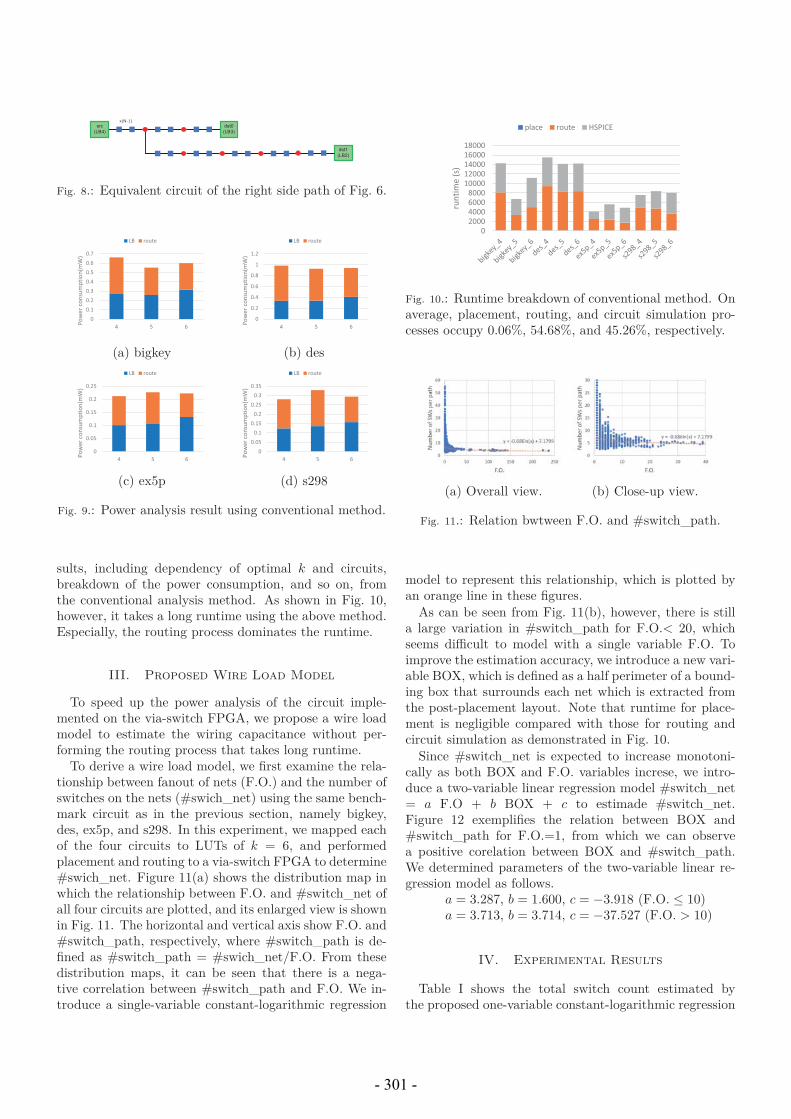
crossbar. In power consumption analysis, a via-switch inthe OFF-state contributes as a parasitic capacitance. Asshown in Fig. 3, the parasitic capacitance per switch inthe OFF-state is 0.56 fF, so the parasitic capacitance pertrack is 0.56(N − 1) fF. Similarly, the equivalent circuitof the fan-out 2 path in the right side of Fig. 6 is asshown in Fig.8. In this way, if netlist is created using eachelement obtained by placement and routing results, powerconsumption can be calculated by performing HSPICEsimulation.
In this study, we use 0-1-A-A LUTs with k=4, 5, and6 with inverters whose sizes are optimized in terms of theenergy-delay product (ED product). We set N = 100.We set the tile array size for each circuit so that wiringcompletes successfully.
F. Power analysis using naive method and its problem
As outlined in the previous section, we can obtain poweranalysis results by generating the net list and conductingcircuit simulation using HSPICE. A power consumptionanalysis example are illustrated in Fig. 9. Power con-sumption analysis results for four relatively similar scalecircuits, bigkey, des, ex5p, and s298 from the MCNCbenchmark are shown in Fig. 9(a), (b), (c), and (d), re-spectively. This figure shows the breakdown of the powerconsumption of LB and wiring resources when each cir-cuit is placed and routed on a via-switch FPGA with LUTsize k being 4, 5, and 6. Here, the target process is theSOTB 65 nm process, the supply voltage 0.55 V, and thetemperature 27 ◦C. Power consumption was analyzed byapplying a random pattern of sufficient sequence length.
As demonstrated in Fig. 9, we can obtain valuable re-
- 300 -
src(LB4)
���� !dst0(LB3)
dst1(LB2)
Fig. 8.: Equivalent circuit of the right side path of Fig. 6.
��� ������������������
� � ����
����
����
����
���
�
!" ����
�
���
���
���
��#
��
� � ����
����
����
����
���
�
!" ����
(a) bigkey (b) des
�
����
��
�� �
���
����
� � ����
����
����
����
���
�
!" ����
�������
�� ����
�������
����
� � ����
����
����
����
���
�
!" ����
(c) ex5p (d) s298
Fig. 9.: Power analysis result using conventional method.
sults, including dependency of optimal k and circuits,breakdown of the power consumption, and so on, fromthe conventional analysis method. As shown in Fig. 10,however, it takes a long runtime using the above method.Especially, the routing process dominates the runtime.
III. Proposed Wire Load Model
To speed up the power analysis of the circuit imple-mented on the via-switch FPGA, we propose a wire loadmodel to estimate the wiring capacitance without per-forming the routing process that takes long runtime.
To derive a wire load model, we first examine the rela-tionship between fanout of nets (F.O.) and the number ofswitches on the nets (#swich_net) using the same bench-mark circuit as in the previous section, namely bigkey,des, ex5p, and s298. In this experiment, we mapped eachof the four circuits to LUTs of k = 6, and performedplacement and routing to a via-switch FPGA to determine#swich_net. Figure 11(a) shows the distribution map inwhich the relationship between F.O. and #switch_net ofall four circuits are plotted, and its enlarged view is shownin Fig. 11. The horizontal and vertical axis show F.O. and#switch_path, respectively, where #switch_path is de-fined as #switch_path = #swich_net/F.O. From thesedistribution maps, it can be seen that there is a nega-tive correlation between #switch_path and F.O. We in-troduce a single-variable constant-logarithmic regression
�������������#���
���� ���� ���� ���� #���
����
���
��
�$%� ���� &'�(�)
Fig. 10.: Runtime breakdown of conventional method. Onaverage, placement, routing, and circuit simulation pro-cesses occupy 0.06%, 54.68%, and 45.26%, respectively.
(a) Overall view. (b) Close-up view.
Fig. 11.: Relation bwtween F.O. and #switch_path.
model to represent this relationship, which is plotted byan orange line in these figures.
As can be seen from Fig. 11(b), however, there is stilla large variation in #switch_path for F.O.< 20, whichseems difficult to model with a single variable F.O. Toimprove the estimation accuracy, we introduce a new vari-able BOX, which is defined as a half perimeter of a bound-ing box that surrounds each net which is extracted fromthe post-placement layout. Note that runtime for place-ment is negligible compared with those for routing andcircuit simulation as demonstrated in Fig. 10.
Since #switch_net is expected to increase monotoni-cally as both BOX and F.O. variables increse, we intro-duce a two-variable linear regression model #switch_net= a F.O + b BOX + c to estimade #switch_net.Figure 12 exemplifies the relation between BOX and#switch_path for F.O.=1, from which we can observea positive corelation between BOX and #switch_path.We determined parameters of the two-variable linear re-gression model as follows.
a = 3.287, b = 1.600, c = −3.918 (F.O. ≤ 10)a = 3.713, b = 3.714, c = −37.527 (F.O. > 10)
IV. Experimental Results
Table I shows the total switch count estimated bythe proposed one-variable constant-logarithmic regression
- 301 -
TABLE I: Estimated total switch count and relative error
Fig. 12.: Relation between BOX and #switch_path whenF.O.=1.
model (post-synthesis) and two-variable linear regressionmodel (post-placement) with actual total switch count(post-routing) for comparison. We used four circuits(bigkey, des, ex5p, s298) and three LUT sizes k = 4,5, and 6 for the experiment. As shown in Table I, theestimation error of the total switch count ranges from−9.1% to 3.2% for the post-synthesis model, and from−7.3% to 7.0% for the post-placement model. Table IIshows the standard deviation of the relative estimationerror of the proposed models. As can be seen from Ta-ble II, the post-placement model is superior in accuracyover the post-synthesis model.
Figure 13 shows the estimated power consumption bythe proposed post-placement model in comparison withthose using post-routing (actual) #switch. The estima-tion error is 47.0% in the worst case. Note that thepost-placement model successfully identifies an architec-ture parameter k that achieves the minimum power foreach circuit.
TABLE II: Standard deviation of the estimation error
Figure 14 shows the comparison of the runtime for esti-mating the power consumption of via-switch FPGA withk = 4 using the proposed post-placement circuit simula-tion flow (model) with the post-routing (actual) simula-tion flow. The execution time is significantly reduced inall four circuits, and 71% in the best case.
V. Conclusion
In this paper, we proposed a wire load model for via-switch FPGA derived from actual placement-and-routingresults of circuits and present the experimental results ofpower estimation accuracy and runtime using the model.The standard deviation of the relative estimation erroron the number of switches calculated by the proposedpost-placement model is 15.0% in the worst case, whilethat of the post-synthesis model is 46.6%. Using the pro-posed post-placement simulation flow, runtime for powerestimation is reduced by 63.8% on average compared withthe conventional post-routing simulation flow, with 11.8%degradation of estimation error on average. As a fu-
- 302 -
�
���
���
���
��#
���
����
����
����
���
�
!" ����
������������#
��
���
����
����
����
���
�
!" ����
(a) bigkey (b) des
�������
�� ����
�������
���
����
����
����
���
�
!" ����
�������
�� ����
�������
�������
���
����
����
����
���
�
!" ����
(c) ex5p (d) s298
Fig. 13.: Comparison of estimated power
�������������#���
���� ���� ���� ���� #���
����
���
��
�$%� ���� &'�(�)
Fig. 14.: Comparison of runtime
ture work, it is desirable to extend the applicability ofthe model to the via-switch FPGAs including arithmeticblocks (or DSP blocks). By quantitative analysis of thepower consumption of the entire circuit implemented ona via-switch FPGA using our model, further developmentsuch as effective power optimization method is expected.
Acknowledgement
This work was supported by JST CREST under GrantJPMJCR1432. This work was also supported by VLSIDesign and Education Center (VDEC), the University ofTokyo in collaboration with Synopsys, Inc.
References
[1] I. Kuon and J. Rose, “Measuring the gap betweenFPGAs and ASICs,” IEEE Trans. on Computer-Aided Design of Integrated Circuits and Systems(TCAD), vol.26, no.2, pp.203–215, 2007.
[2] N. Banno, T. Sakamoto, M. Tada, M. Miyamura,Y. Yabe, Y. Saito, S. Ishida, K. Okamoto, H. Hada,
N. Kasai, N. Iguchi, and M. Aono, “Reliable solid-electrolyte crossbar switch for programmable logicdevice,” Proceedings of Symposium on VLSI Tech-nology, pp.115–116, 2010.
[3] M. Miyamura, M. Tada, T. Sakamoto, N. Banno, K.Okamoto, N. Iguchi, and H. Hada, “First demonstra-tion of logic mapping on nonvolatile programmablecell using complementary atom switch,” Proceed-ings of IEEE International Electron Devices Meeting(IEDM), pp.10.6.1–10.6.4, 2012.
[4] T. Higashi and H. Ochi, “Area-efficient LUT-like pro-grammable logic using atom switch and its mappingalgorithm,” Proceedings of 15th International Sym-posium on Communications and Information Tech-nologies (ISCIT), pp.201–204, 2015.
[5] A. Natsuhara, T. Imagawa, and H. Ochi, “A studyon the power efficiency of via-switch oriented pro-grammable logic 0-1-A-A LUT,” IEICE Tech. Rep.,vol.117, no.377, pp.107–112, 2018. (in Japanese).
[6] M. Miyamura, T. Sakamoto, Y. Tsuji, M. Tada, N.Banno, K. Okamoto, N. Iguchi, and H. Hada, “0.5-Vhighly power-efficient programmable logic using non-volatile configuration switch in BEOL,” Proceedingsof International Symposium on Field-ProgrammableGate Arrays (FPGA), pp.236–239, 2015.
[7] N. Banno, M. Tada, K. Okamoto, N. Iguchi, T.Sakamoto, M. Miyamura, Y. Tsuji, H. Hada, H. Ochi,H. Onodera, M. Hashimoto, and T. Sugibayashi,“A novel two-varistors (a-Si/SiN/a-Si) selected com-plementary atom switch (2V-1CAS) for nonvolatilecrossbar switch with multiple fan-outs,” Proceed-ings of IEEE International Electron Devices Meeting(IEDM), pp.2.5.1–2.5.4, Dec. 2015.
[8] J. Hotate, T. Kishimoto, T. Higashi, H. Ochi, R. Doi,M. Tada, T. Sugibayashi, K. Wakabayashi, H. On-odera, Y.Mitsuyama, and M. Hashimoto, “A highly-dense mixed grained reconfigurable architecture withoverlay crossbar interconnect using Via-switch,” Pro-ceedings of International Conference on Field Pro-grammable Logic and Applications (FPL), pp.272–275, 2016.
[9] A. Rahman and V. Polavarapuv, “Evaluation of low-leakage design techniques for field programmablegate arrays,” Proceedings of International Sympo-sium on Field-Programmable Gate Arrays (FPGA),pp.23–30, 2004.
[10] F. Li, Y. Lin, L. He, and J. Cong, “Low-powerFPGA using pre-defined dual-Vdd/dual-Vt fabrics,”Proceedings of International Symposium on Field-Programmable Gate Arrays (FPGA), pp.42–50,2004.