47
5/2/2005 1 FLCC Wireless Metrology in Semiconductor Manufacturing Costas J. Spanos FLCC Seminar 5/2/2005
5/2/2005
1
FLCC
Wireless Metrology in Semiconductor Manufacturing
Costas J. SpanosFLCC Seminar
5/2/2005
5/2/2005
2
FLCC
Outline
Historical perspective• Hardware and software applications• Breakthroughs that have yet to be realized• Distributed control and diagnostics• Hardware requirements
5/2/2005
3
FLCC
Past And Present
• Ideas and even patents circulated in the industry since the early 90s.– No known implementation since UCB work started in
late 1997• Commercialized in 2000 by OnWafer
Technologies– Founders from UCB and LAM Research– BakeTemp for Post Exposure Bake– PlasmaTemp– An expanding software applications suite
5/2/2005
4
FLCC
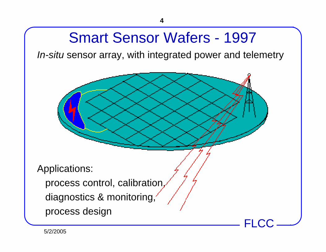
Smart Sensor Wafers - 1997In-situ sensor array, with integrated power and telemetry
Applications:process control, calibration, diagnostics & monitoring,process design
5/2/2005
5
FLCC
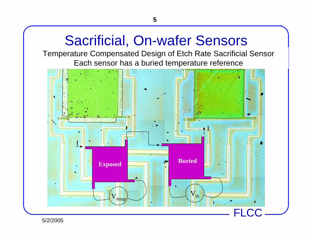
Sacrificial, On-wafer Sensors
I
Exposed
I
Buried
VthVtemp
Temperature Compensated Design of Etch Rate Sacrificial SensorEach sensor has a buried temperature reference

5/2/2005
6
FLCC
Wired Proof of Concept Implementation
100mm

5/2/2005
7
FLCC
• Wafer placed on bakeplate, Rs measured for both sensorsResults - bakeplate
5/2/2005
8
FLCC
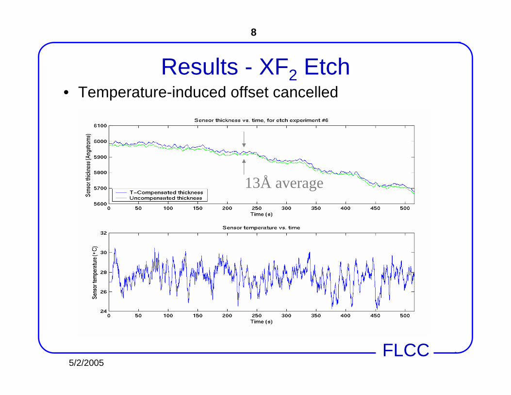
Results - XF2 Etch• Temperature-induced offset cancelled
13Å average

5/2/2005
9
FLCC
Wireless Prototype ~1999Off-the Shelf Components, Ni on Al, Solder Paste
Mount…
thermistorresistor capacitors
PIC
voltage regulatorLED
batteries
100mm
4 Sensors4oC Accuracy2oC Precision1oC ResolutionPrimary BatteriesNo MemoryFixed Behavior~15grams/ 5mm
4 Sensors4oC Accuracy2oC Precision1oC ResolutionPrimary BatteriesNo MemoryFixed Behavior~15grams/ 5mm

5/2/2005
10
FLCC
Thermal Stress Tests on Calibrated Plate

5/2/2005
11
FLCC
Autonomous Passage Through Wafer Track
Wafer leaves bake plateWafer leaves bake plate
Wafer arrives at chill plateWafer arrives at chill plate
Non-uniform bake…Non-uniform bake…
Non-uniform coolingNon-uniform cooling
5/2/2005
12
FLCC
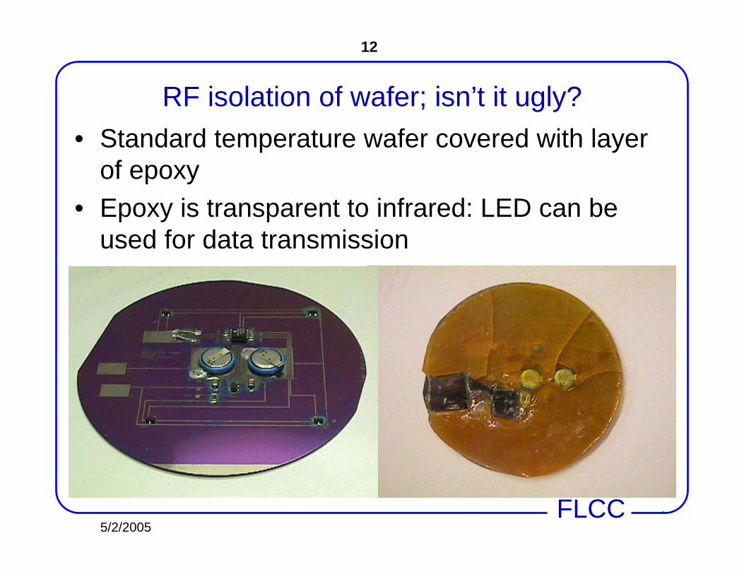
RF isolation of wafer; isn’t it ugly?• Standard temperature wafer covered with layer
of epoxy• Epoxy is transparent to infrared: LED can be
used for data transmission

5/2/2005
13
FLCC
Test results in plasma: RF 50W, 0.76 Torr, O2
sensor 3
sensor 1 sensor 2
sensor 4
Word’s first Wireless Plasma Monitoring – Late 1999!
5/2/2005
14
FLCC
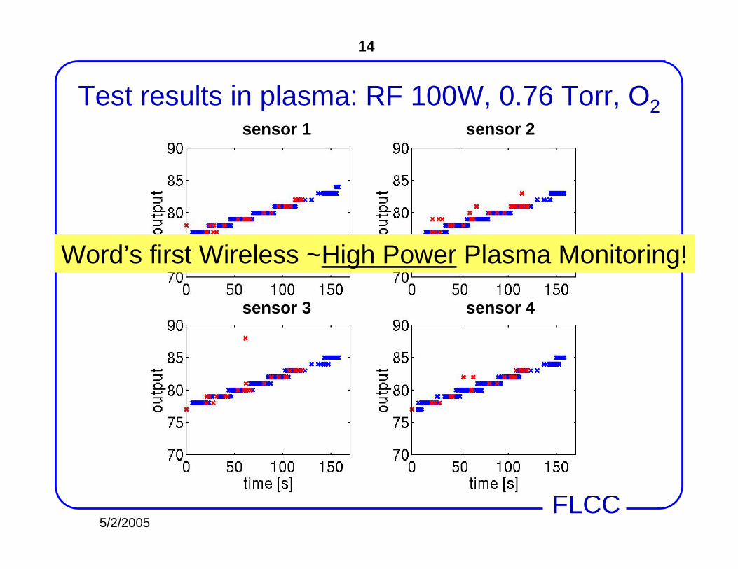
Test results in plasma: RF 100W, 0.76 Torr, O2
sensor 3
sensor 1 sensor 2
sensor 4
Word’s first Wireless ~High Power Plasma Monitoring!
5/2/2005
15
FLCC
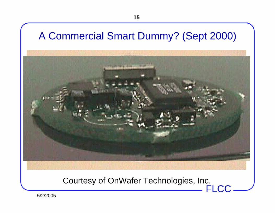
A Commercial Smart Dummy? (Sept 2000)
Courtesy of OnWafer Technologies, Inc.

5/2/2005
16
FLCC
Outline
• Historical perspectiveHardware and software applications
• Breakthroughs that have yet to be realized• Distributed control and diagnostics that go beyond
lithography and etch• Hardware requirements

5/2/2005
17
FLCC
Today: The BakeTemp Sensor Wafer
module
SiO2polyimid
Courtesy OnWafer Technologies
19994 Sensors4oC Accuracy2oC Precsion1oC ResolutionPrimary BatteriesNo MemoryFixed Behavior~15grams/ 5mm
19994 Sensors4oC Accuracy2oC Precsion1oC ResolutionPrimary BatteriesNo MemoryFixed Behavior~15grams/ 5mm
200564 Sensors0.05oC Accuracy0.02oC Precision0.001oC ResolutionSecondary BatteriesMemoryProgrammable/Adaptive Behavior~1.5grams/ 3mm
200564 Sensors0.05oC Accuracy0.02oC Precision0.001oC ResolutionSecondary BatteriesMemoryProgrammable/Adaptive Behavior~1.5grams/ 3mm
5/2/2005
18
FLCC
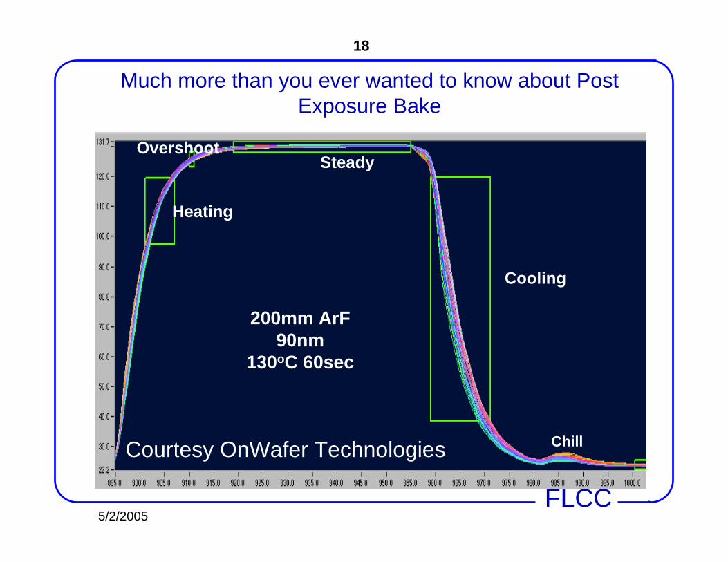
Much more than you ever wanted to know about Post Exposure Bake
Overshoot
Cooling
Steady
Heating
Chill
200mm ArF90nm
130oC 60sec
Courtesy OnWafer Technologies

5/2/2005
19
FLCC
Today: The PlasmaTemp Sensor Wafer
Demonstrated in up to 7,000W ChambersReusableClean and safe enough to be adopted by all the top tier fabs

5/2/2005
20
FLCC
On-Wafer Plasma Monitoring200mm Poly Etching
Routine He Reduced He
pre-etchpre-etch
main etchmain etch
de-chuckde-chuckover etchover etch
5/2/2005
21
FLCC
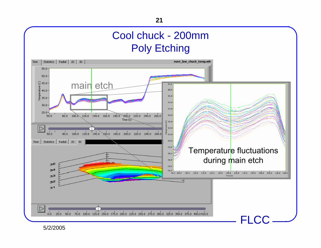
Cool chuck - 200mm Poly Etching
main etch
Temperature fluctuations during main etch

5/2/2005
22
FLCC
Can see rotating magnetic field !
phase delay in temp fluctuationCan calculate B-field periodCan see rotation is clockwise
5/2/2005
23
FLCC
What are the Killer Apps?• Temperature Monitoring has intuitive diagnostic
value for some users.• To expand use from Pilot to Production, we must
address different, routine needs.– Calibration– Acceptance– SPC/SQC– …
5/2/2005
24
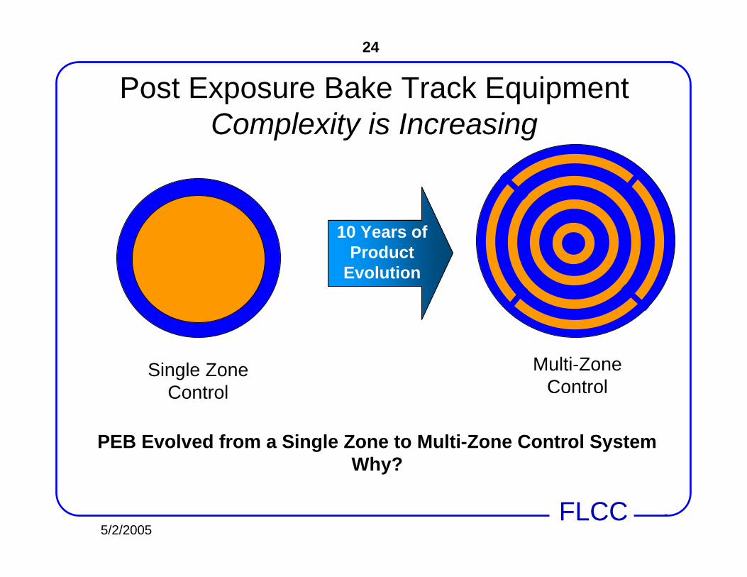
FLCC
PEB Evolved from a Single Zone to Multi-Zone Control System Why?
Multi-Zone Control
Single Zone Control
10 Years of Product
Evolution
Post Exposure Bake Track Equipment Complexity is Increasing
5/2/2005
25
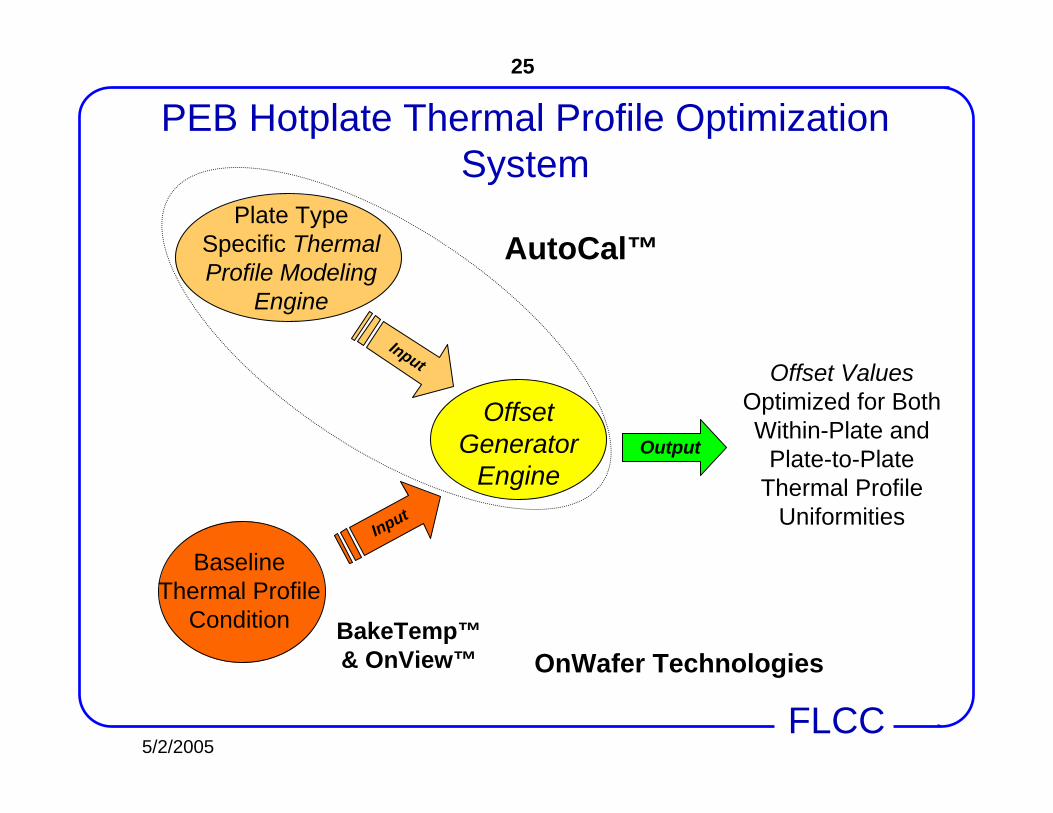
FLCC
PEB Hotplate Thermal Profile Optimization System
Baseline Thermal Profile
Condition
Offset Generator
Engine
Plate Type Specific Thermal Profile Modeling
Engine
Offset ValuesOptimized for Both Within-Plate and
Plate-to-Plate Thermal Profile
Uniformities
Output
Input
BakeTemp™& OnView™
AutoCal™
Input
OnWafer Technologies

5/2/2005
26
FLCC
PEB Temp Control
16 plates, 120 ºC Target
2.700oC
Target = 120oC
0.175oC
Before After
OnWafer Technologies

5/2/2005
27
FLCC
Spatial PEB/CD Distribution Correlation• Plotting both the bake plate temperature trajectory and R2
from temperature-CD correlation against bake time:
Max R2 during the transient heating period
Continued high R2
during steady state due to poor temperature control in single-zone plate design
• Plotting both the bake plate temperature trajectory and R2
from temperature-CD correlation against bake time:
Max R2 during the transient heating period
Continued high R2
during steady state due to poor temperature control in single-zone plate design

5/2/2005
28
FLCC
PEB Hotplate Critical Dimension Optimization System
Baseline Thermal Profile
Condition
Offset Generator
Engine
Plate Type Specific Thermal Profile Modeling
Engine
Offset ValuesOptimized for Both Within-Plate and
Plate-to-Plate Critical Dimensions
Uniformities
Output
Input
BakeTemp™& OnView™
AutoCal™
Input
Input
Resist & Litho Cell Specific CD
Modeling Engine
AutoCD™
Baseline CD Profiles per Plate Customer
Provided
Input
OnWafer Technologies

5/2/2005
29
FLCC
CDU Improvement
AcrossPlate Plate to
Plate
AutoCD
AutoCalPOR
0
0.5
1
1.5
2
2.5
3
3.5
AutoCDAutoCalPOR
OnWafer Technologies

5/2/2005
30
FLCC
What we learned about Lithography• Weight / Form Factor
– module electronics, height, wafer flatness• Precision• Speed• Equipment Compatibility• Contamination
• COST OF OWNERSHIP– Lifetime– Ease of Use
5/2/2005
31
FLCC
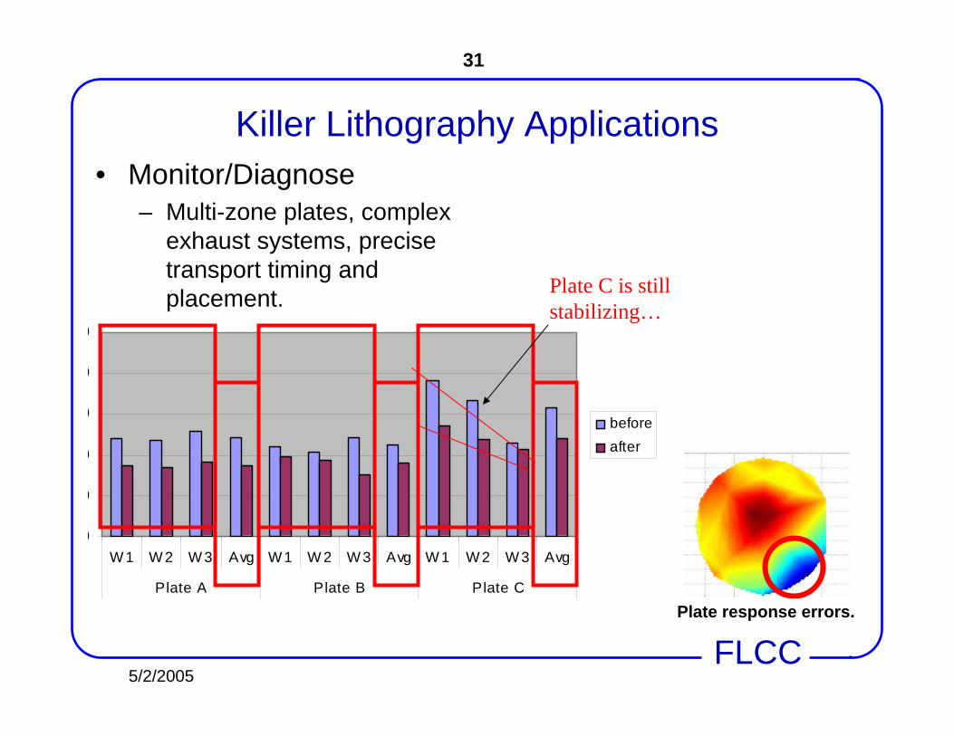
0
0
0
0
0
0
W 1 W 2 W 3 Avg W 1 W 2 W 3 Avg W 1 W 2 W 3 Avg
Plate A Plate B Plate C
beforeafter
Killer Lithography Applications• Monitor/Diagnose
– Multi-zone plates, complex exhaust systems, precise transport timing and placement. Plate C is still
stabilizing…
Plate response errors.

5/2/2005
32
FLCC
What we learned from Plasma
• RF/heat tolerance• Arcing resistance• Shape/size• Contamination• Lifetime and reliability

5/2/2005
33
FLCC
Killer Plasma Apps
• Temperature monitoring• Automatic Calibration/Diagnosis???• Equipment Compatibility
– Power Range– RF Tolerance– Chemistry– Contamination– Arcing Tolerance

5/2/2005
34
FLCC
Outline
• Historical perspective• Hardware and software applications
Breakthroughs that have yet to be realized• Distributed control and diagnostics• Hardware requirements
5/2/2005
35
FLCC
The limitations• Shape, Size and Weight
– Surface mount electronics – min ~2mm– Needs thin film wafer interconnect to achieve ~10µm
flatness– Integrated (in Si) electronics still prohibitive for a
consumable product• Lifetime
– Battery– Films (Plasma, CMP)
• Performance Envelope– Battery up to 200oC– Electronics up to 300oC
5/2/2005
36
FLCC
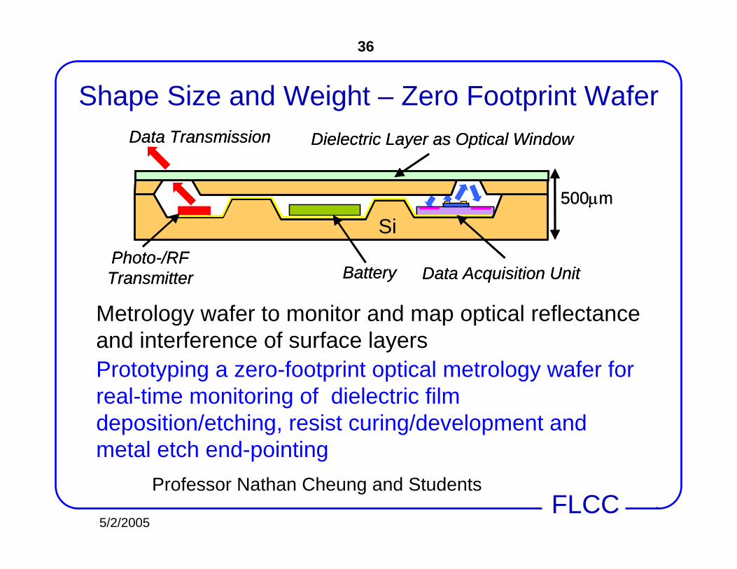
Shape Size and Weight – Zero Footprint Wafer
Prototyping a zero-footprint optical metrology wafer for real-time monitoring of dielectric film deposition/etching, resist curing/development and metal etch end-pointing
Metrology wafer to monitor and map optical reflectance and interference of surface layers
Data Transmission
Photo-/RF Transmitter
Dielectric Layer as Optical Window
Battery Data Acquisition Unit
500µm
Si
Data Transmission
Photo-/RF Transmitter
Dielectric Layer as Optical Window
Battery Data Acquisition Unit
500µm
Si
Professor Nathan Cheung and Students

5/2/2005
37
FLCC
Lifetime• Batteries
– Button cell secondary commercial solutions not available above 80oC.
– Primary solutions are a bit bulky but can go up to 140oC.– Lithium-based thin film technologies still immature, not focused
on high temp applications.– Temporary solution: screen commercial batteries, make them
field replaceable (160oC ceiling, 10s of hours of operation)– Long term solution: wait for high temperature cathode thin film
batteries (~200oC ceiling, 100s of hours)
• Films– Inherent Limitation in Etch – just make it thick and provide visible
“thread wear” marks.– Might be replaceable in CMP

5/2/2005
38
FLCC
Performance Envelope• High Temperature Electronics
– Off the shelf electronics (surface mount or hybrid) ~ 180oC.
– Off the shelf electronics with custom clocking ~240oC.• High Temperature Batteries will probably not
happen above 200oC– Parasitic power sources / caps
5/2/2005
39
FLCC
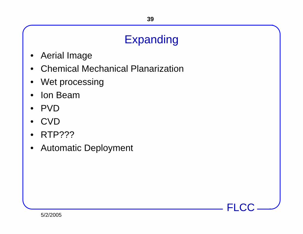
Expanding• Aerial Image• Chemical Mechanical Planarization• Wet processing• Ion Beam• PVD• CVD• RTP???• Automatic Deployment
5/2/2005
40
FLCC
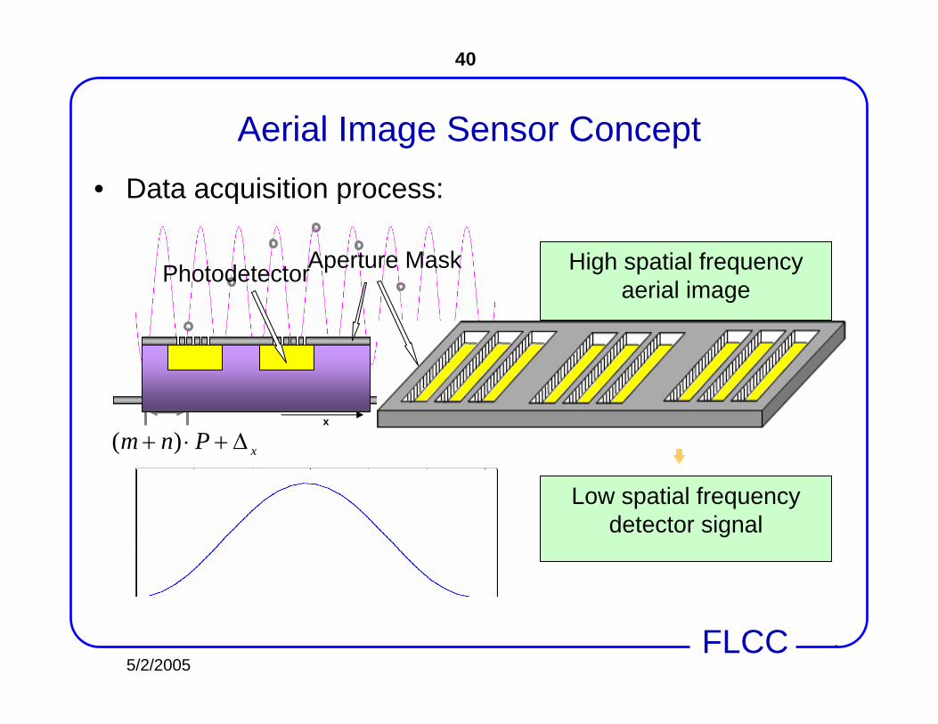
Aerial Image Sensor Concept• Data acquisition process:
High spatial frequency aerial image
Aperture mask transmission
Low spatial frequency detector signal
x
xPnm ∆+⋅+ )(
Aperture MaskPhotodetector

5/2/2005
41
FLCC
x
xPnm ∆+⋅+ )(
Choosing Aperture Width & Thickness (cont.)
• Near-Field Simulation:
Illumination phase shift 0oIllumination phase shift 180o Aperture groups phase “moving” at max positionAperture groups phase “moving” at min position

5/2/2005
42
FLCC
Outline
• Historical perspective• Hardware and software applications• Breakthroughs that have yet to be realized
Distributed control and diagnostics• Hardware requirements

5/2/2005
43
FLCC
Pattern Transfer Control
Spin
HMDS
PA Bake
Exposure
PEB
Develop
PD Bake
Photoresist Removal
Electrical Testing
Electrical Testing
Poly Etch SystemEtch
Etch
Etch
TemperatureFeed-forward control
TemperatureFeed-forward control
Temperature, Plasma Voltage, Ion CurrentFF/FB Control, chuck diagnostics
Temperature, Plasma Voltage, Ion CurrentFF/FB Control, chuck diagnostics
Aerial ImageAerial Image
ScatterometryProfile InversionFeedback Control
ScatterometryProfile InversionFeedback Control
Thin FilmFB/FF Control
Thin FilmFB/FF Control
ScatterometryFeedback ControlScatterometry
Feedback ControlScatterometryFB/FF ControlScatterometryFB/FF Control

5/2/2005
44
FLCC
Outline
• Historical perspective• Hardware and software applications• Breakthroughs that have yet to be realized• Distributed control and diagnostics
Hardware requirements

5/2/2005
45
FLCC
Automatic Deployment
• Wireless Wafers must resemble “real” wafers as much as possible.
• In a 300mm factory, they must reside in FOUPsand move around via overhead transport.
• Deployment, data collection, analysis and resulting actions must be automated.
5/2/2005
46
FLCC
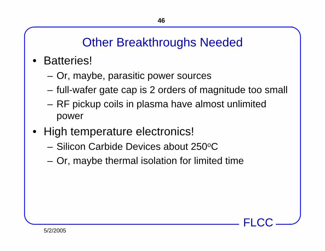
Other Breakthroughs Needed• Batteries!
– Or, maybe, parasitic power sources– full-wafer gate cap is 2 orders of magnitude too small– RF pickup coils in plasma have almost unlimited
power• High temperature electronics!
– Silicon Carbide Devices about 250oC– Or, maybe thermal isolation for limited time
5/2/2005
47
FLCC
Conclusion• Wireless Semiconductors Metrology has gone a
long way since we started in 1998– Three vendors– Officially Adopted by Fabs and Tool Makers– “Best Known Method” (BKM) in several applications
• Target processes remain in Lithography and Etch, but others are not too far behind
• Next generation of “zero footprint” metrology is likely to expand the application base even more


