W.Kucewicz 2004 Nuclear Science Symposium, Rome, October 16-22, 2004 1 Fully Depleted Fully Depleted Monolithic Active Monolithic Active Pixel Sensor in SOI Pixel Sensor in SOI Technology Technology Presented Presented by by Wojciech Kucewicz Wojciech Kucewicz a on behalf of on behalf of A.Bulgheroni A.Bulgheroni b , M. Caccia , M. Caccia b , K. Domanski , K. Domanski c , P. Grabiec , P. Grabiec c , M. Grodner , M. Grodner c , , B. Jaroszewicz B. Jaroszewicz c , M. Jastrzab , M. Jastrzab a , A. Kociubinski , A. Kociubinski c , M. Kozioł, M. Kozioł, K. K. Kucharski Kucharski c , S.Kuta , S.Kuta a , J. Marczewski , J. Marczewski c , H. Niemiec , H. Niemiec a , M. Sapor , M. Sapor a , D. , D. Tomaszewski Tomaszewski c a AGH-Univ. of Science and Technology, Al. Mickiewicza 30, 30-059 Krakow, Poland b Università dell’Insubria, via Valleggio 11, 22100 Como, Italy
Transcript
W.Kucewicz 2004 Nuclear Science Symposium, Rome, October 16-22, 2004 1
Fully Depleted Fully Depleted Monolithic Active Pixel Monolithic Active Pixel
Sensor in SOI Sensor in SOI Technology Technology
Fully Depleted Fully Depleted Monolithic Active Pixel Monolithic Active Pixel
Sensor in SOI Sensor in SOI Technology Technology
PresentedPresented by byWojciech KucewiczWojciech Kucewiczaa
on behalf of on behalf of A.BulgheroniA.Bulgheronibb, M. Caccia, M. Cacciabb, K. Domanski, K. Domanskicc, P. Grabiec, P. Grabieccc, M. Grodner, M. Grodnercc, ,
B. JaroszewiczB. Jaroszewiczcc, M. Jastrzab, M. Jastrzabaa, A. Kociubinski, A. Kociubinskicc,, M. Kozioł, M. Kozioł, K. Kucharski K. Kucharskicc, , S.KutaS.Kutaaa, J. Marczewski, J. Marczewskicc, H. Niemiec, H. Niemiecaa, M. Sapor, M. Saporaa, D. Tomaszewski, D. Tomaszewskicc
a AGH-Univ. of Science and Technology, Al. Mickiewicza 30, 30-059 Krakow, Poland
b Università dell’Insubria, via Valleggio 11, 22100 Como, Italyc Institute of Electron Technology, Al. Lotnikow 32/46, 02-668 Warsaw, Poland
W.Kucewicz 2004 Nuclear Science Symposium, Rome, October 16-22, 2004 2
OutlineOutlineOutlineOutline
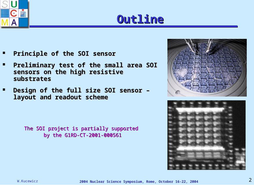
Principle of the SOI sensorPrinciple of the SOI sensor
Preliminary test of the small area SOI Preliminary test of the small area SOI sensors on the high resistive substratessensors on the high resistive substrates
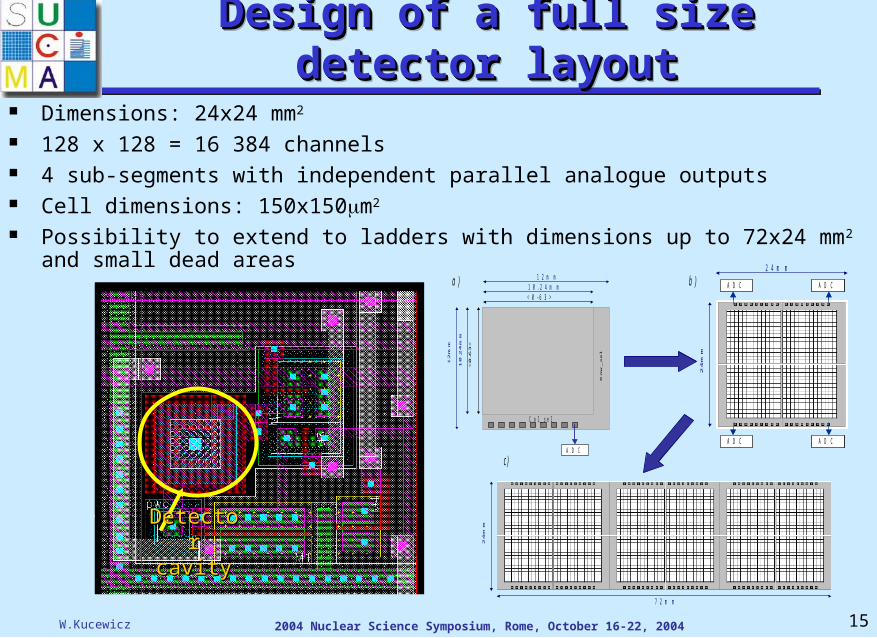
Design of the full size SOI sensor – Design of the full size SOI sensor – layout and readout schemelayout and readout scheme
The SOI project is partially supported The SOI project is partially supported bby y the G1RD-CT-2001-000561the G1RD-CT-2001-000561
W.Kucewicz 2004 Nuclear Science Symposium, Rome, October 16-22, 2004 3
Principle of SOI monolithic Principle of SOI monolithic detectordetector
Principle of SOI monolithic Principle of SOI monolithic detectordetector
The The wafer bondingwafer bonding technics was technics was choosen for SOI technologychoosen for SOI technologyLow resistivity
(9-13 cm, CZ) 1.5 m thick Standard CMOS technology
Detector Detector Support layer High resistive
(> 4 kcm,FZ) 300 m thick Conventional p+-n DC-coupled
W.Kucewicz 2004 Nuclear Science Symposium, Rome, October 16-22, 2004 5
MotivationMotivationMotivationMotivation
As a monolithic device eliminates bump-bonding process and allows As a monolithic device eliminates bump-bonding process and allows reduction of total sensor thickness reduction of total sensor thickness reduction of multiple reduction of multiple scatteringscattering
Allows using high resistive detector substrates and operation in fully Allows using high resistive detector substrates and operation in fully depleted region depleted region good detection efficiency, enables detection of good detection efficiency, enables detection of particles with limited range in the silicon without backthinning particles with limited range in the silicon without backthinning processprocess
Gives possibility to use both type of transistors in readout channels Gives possibility to use both type of transistors in readout channels increased flexibility of the design, design optimisation for different increased flexibility of the design, design optimisation for different applicationapplication
Advantages of Advantages of the the SOI detectors:SOI detectors:
The SOI sensor may merge the advantages of the The SOI sensor may merge the advantages of the monolithic and hybrid detectorsmonolithic and hybrid detectors
Advantages of Advantages of the the SOI detectors:SOI detectors:
The SOI sensor may merge the advantages of the The SOI sensor may merge the advantages of the monolithic and hybrid detectorsmonolithic and hybrid detectors
W.Kucewicz 2004 Nuclear Science Symposium, Rome, October 16-22, 2004 6
Test structures of the SOI Test structures of the SOI detectordetector
Test structures of the SOI Test structures of the SOI detectordetector
W.Kucewicz 2004 Nuclear Science Symposium, Rome, October 16-22, 2004 7
Test structures of the SOI Test structures of the SOI detectordetector
Test structures of the SOI Test structures of the SOI detectordetector
Small readout matrices (8x8) with associated detector diodes or input pads for external signal sources were fabricated on the SOI wafers at the IET, Warsaw
Two readout channel configurations – with NMOS transistor switch (cell dimensions 140x122 m2) and with transmission gate (140x140 m2)
Contact to the detector placed in the V-shape cavity.
Row selection signals led by two parallel lines with opposite polarization, body of the structure densely grounded reduction of the cross-talk between the electronics and detector
VDET
VSS
VDD
IN
RES
N_ROW_SEL
ROW_SEL
COL
W.Kucewicz 2004 Nuclear Science Symposium, Rome, October 16-22, 2004 8
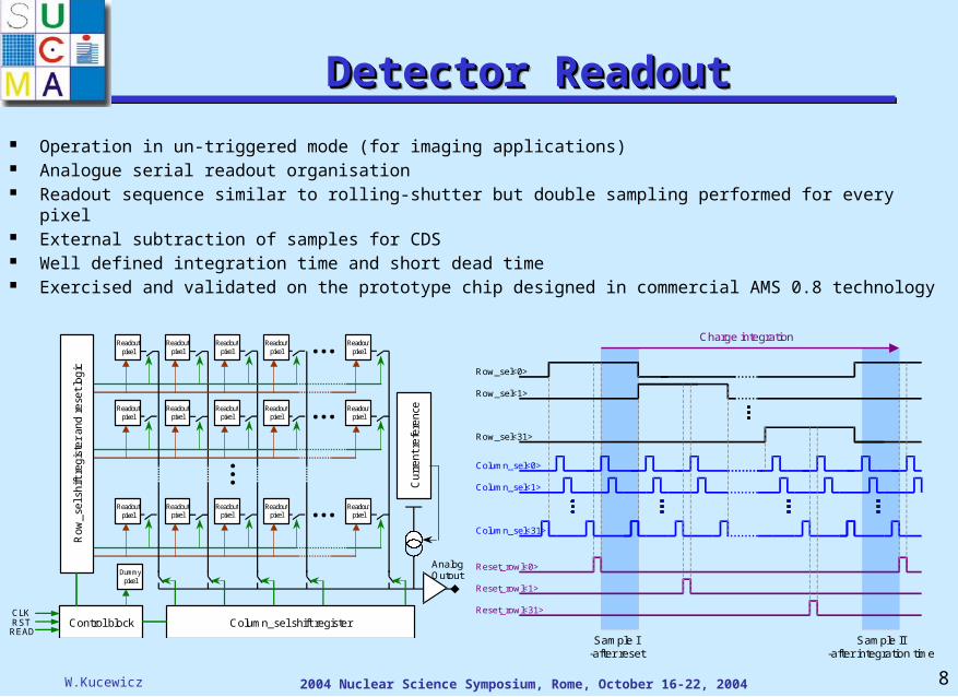
Operation in un-triggered mode (for imaging applications) Analogue serial readout organisation Readout sequence similar to rolling-shutter but double sampling performed for every pixel External subtraction of samples for CDS Well defined integration time and short dead time Exercised and validated on the prototype chip designed in commercial AMS 0.8 technology
Readout pixel
Readout pixel
Readout pixel
Readout pixel
Readout pixel
Readout pixel
Readout pixel
Readout pixel
Readout pixel
Readout pixel
Readout pixel
Readout pixel
Readout pixel
Readout pixel
Readout pixel
Ro
w_
sel s
hift
reg
iste
r an
d r
ese
t lo
gic
Analog Output
Column_sel shift register
Dummy pixel
Control block CLK RST
READ
Cu
rre
nt r
efe
ren
ce
Row_sel<0>
Column_sel<0>
Column_sel<1>
Column_sel<31>
Reset_rowl<0>
Row_sel<1>
Row_sel<31>
Reset_rowl<1>
Reset_rowl<31>
Sample I-after reset
Sample II-after integration time
Charge integration
W.Kucewicz 2004 Nuclear Science Symposium, Rome, October 16-22, 2004 9
SUCIMA Imager DAQ for the SOI SUCIMA Imager DAQ for the SOI DetectorDetector
SUCIMA Imager DAQ for the SOI SUCIMA Imager DAQ for the SOI DetectorDetector
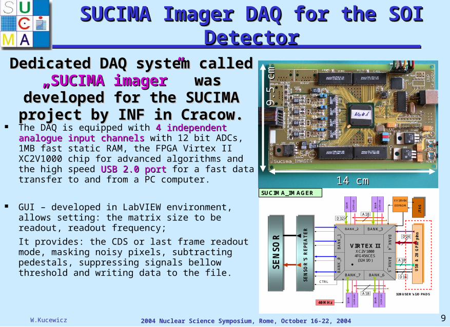
The DAQ is equipped with 4 independent analogue 4 independent analogue inputinput channels channels with 12 bit ADCs, 1MB fast static RAM, the FPGA Virtex II XC2V1000 chip for advanced algorithms and the high speed USB 2.0 USB 2.0 portport for a fast data transfer to and from a PC computer.
GUI – developed in LabVIEW environment, allows setting: the matrix size to be readout, readout frequency;
It provides: the CDS or last frame readout mode, masking noisy pixels, subtracting pedestals, suppressing signals bellow threshold and writing data to the file.
VIRTEX IIXC2V1000
4FG456CES(324 I/O)
VIRTEX IIXC2V1000
4FG456CES(324 I/O)
40 MHz
BANK_7S
EN
SO
R
SUCIMA_IMAGER
BANK_2 BANK_3
BA
NK
_5B
AN
K_4
BANK_6
BA
NK
_0B
AN
K_1
SR
AM
2x2
56K
x16
B
SR
AM
2x2
56K
x16
B
US
B &
28
GP
IO p
ins
D32A18
D24
D16
.
JTA
G
A18
A18CLK
CTRL
328 USER’s I/O PADS
SE
NS
OR
’S R
EP
EA
TE
R
SR
AM
2x2
56K
x16
B
SR
AM
2x2
56K
x16
B XV18V04
EEPROM
DedicatedDedicated DAQ system called DAQ system called „SUCIMA imager”„SUCIMA imager” was was
developeddeveloped for the SUCIMA for the SUCIMA projectproject by INF in Cracow by INF in Cracow..
14 cm14 cm
9.5
cm
9.5
cm
W.Kucewicz 2004 Nuclear Science Symposium, Rome, October 16-22, 2004 10
Stand Alone DetectorStand Alone Detector Diodes and Diodes and Electronics withElectronics with Input PadsInput Pads
Stand Alone DetectorStand Alone Detector Diodes and Diodes and Electronics withElectronics with Input PadsInput Pads
Transfer characteristics were measured with external voltage pulse signal
with NMOS transistor switch Measured DC output dynamic range up
to 1.0 V with transmission gate
Measured DC output dynamic range up to 1.8 V non-linearity at the middle range was reduced in the latest designs
Readout ElectronicsReadout Electronics
1.0E-12
1.0E-11
1.0E-10
1.0E-09
0 10 20 30 40 50 60Detector bias [V]
Le
ak
ag
e c
urr
en
t [
A/m
m2 ]
e7 g8
1.0E-12
1.0E-11
1.0E-10
1.0E-09
0 10 20 30 40 50 60Detector bias [V]
Le
ak
ag
e c
urr
en
t [
A/m
m2 ]
e7 g8
Pixel leakage current: From 200 nA down to 10 nA per
cm2 depending on the process
Detector full depletion voltage: 60 V down to 50 V for different
iterations
Detector DiodesDetector Diodes
Comparison of transfer characteristics of readout matrices on SOI wafers
particles passing through detector active volume (each corresponding to 3.4 MIP)
Integration time = 1 ms Detector polarization=60V 10 000 events recorded and averaged Input signal scaled assuming the
sensor gain of 11mV/MIP
GGood detector sensitivity for the ionising radiation and ood detector sensitivity for the ionising radiation and linear response as a function of the generated charge was linear response as a function of the generated charge was
observedobserved..
Linearity of Sensor ResponseLinearity of Sensor Response
12
Tests with theTests with the 90 90 Sr Beta SourceSr Beta SourceTests with theTests with the 90 90 Sr Beta SourceSr Beta Source Sensor sensitivity tested with 90Sr beta
source Measurements conditions: complete
depletion (Vdet= 70 V), integration time: Tint = 720 s, source placed at the top of the sensor.
Detector output signal amplified (k2.5) before digitalisations
On-line CDS processing, off-line pedestal subtraction, common mode suppression and cluster search
Recorded EventRecorded EventRecorded EventRecorded Event Cluster SizeCluster SizeCluster SizeCluster Size
Gaussian distribution of the noise
Landau distribution of the measured
signals
The most probably value of signal per MIP: 27 ADC 27 ADC
Noise for the seed pixels: 1.5 to 2 ADC1.5 to 2 ADC
W.Kucewicz 2004 Nuclear Science Symposium, Rome, October 16-22, 2004 13
Tests with theTests with the Alpha Particles Alpha ParticlesTests with theTests with the Alpha Particles Alpha Particles
Alpha source placed at the distance of 1 cm from the detector backplane Initial energy of particles = 5.5 MeV Detector fully depleted (VD=70V), integration time 720 s On-line CDS processing, off-line pedestal subtraction, common mode suppression and
cluster search
W.Kucewicz 2004 Nuclear Science Symposium, Rome, October 16-22, 2004 14
Typical measured cluster pulse height cluster pulse height 200 ADC 200 ADC – corresponding to about half of the alpha particles initial energy.
Pedestal width – about 1.5 ADC1.5 ADC, S/N for cluster pulse height 130. Broad spectrum due to energy straggling in air.
W.Kucewicz 2004 Nuclear Science Symposium, Rome, October 16-22, 2004 17
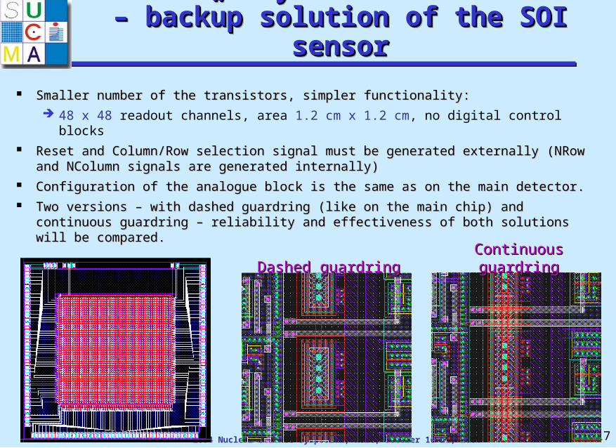
„„Baby Detector” Baby Detector” – backup solution of the SOI – backup solution of the SOI
sensorsensor
„„Baby Detector” Baby Detector” – backup solution of the SOI – backup solution of the SOI
sensorsensor
Smaller number of the transistors, simpler functionality: Smaller number of the transistors, simpler functionality: 48 x 48 readout channels, area 1.2 cm x 1.2 cm, no digital control blocks
Reset and Column/Row selection signal must be generated externallyReset and Column/Row selection signal must be generated externally ( (NRow NRow and NColumn signals are generated internallyand NColumn signals are generated internally))
Configuration of the analogue blockConfiguration of the analogue block is is the same as on the main detector the same as on the main detector.. Two versions – with dashed guardring (like on the main chip) and continuous Two versions – with dashed guardring (like on the main chip) and continuous
guardring – reliability and effectiveness of both solutions will be compared.guardring – reliability and effectiveness of both solutions will be compared.
W.Kucewicz 2004 Nuclear Science Symposium, Rome, October 16-22, 2004 18
NewNew Test Structure Test StructureNewNew Test Structure Test Structure
Several units of the old test structure for the crosscheck of the parameters between different wafers
Several units with different transistor layouts for matching, noise and radiation hardness studies
Test structure for direct IV and CV characteristics measurements of the detector diodes
Small matrix of the sensor with modified readout configuration
New Test Structure exploits the experience gained with the old test
structure. It consists of:
W.Kucewicz 2004 Nuclear Science Symposium, Rome, October 16-22, 2004 19
NewNew Test Structure Test StructureNewNew Test Structure Test Structure Matrix of 16x16 readout channels with
reduced capacitance at the input node – higher signal per MIP
Readout electronics configuration the same like on the main sensor
Input (charge integrating) capacitance reduced by disconnecting the polySi plate covering pixel cavity from the input and connection to the VSS (in case of the short between input and polySi layer no negative influence of the faulty pixel on the neighbours performance).
Estimated pixel contact capacitance: Cpixcon 27 fF, estimated total input capacitance: Ctot 190 fF signal per MIP: S 14 15 mV
This circuit was also placed separately (outside Test Structure chip) at several localization on the wafer – another backup solution in case of the problems with the big detectors.
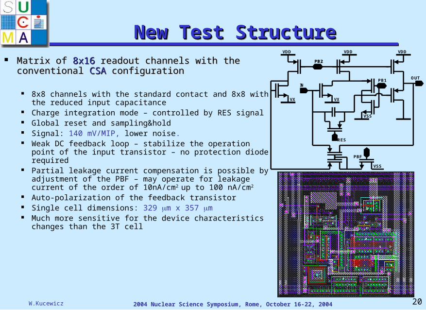
W.Kucewicz 2004 Nuclear Science Symposium, Rome, October 16-22, 2004 20
NewNew Test Structure Test StructureNewNew Test Structure Test Structure Matrix of Matrix of 8x168x16 readout channels with readout channels with the the
8x8 channels with the standard contact and 8x8 with the reduced input capacitance
Charge integration mode – controlled by RES signal Global reset and sampling&hold Signal: 140 mV/MIP, lower noise. Weak DC feedback loop – stabilize the operation
point of the input transistor – no protection diode required
Partial leakage current compensation is possible by adjustment of the PBF – may operate for leakage current of the order of 10nA/cm2 up to 100 nA/cm2
Auto-polarization of the feedback transistor Single cell dimensions: 329 m x 357 m Much more sensitive for the device characteristics
changes than the 3T cell
VX VX
IN
VDD VDD
PB2
PB1
VSS
RES
VDD
OUT
PB2
PBF
VSS
W.Kucewicz 2004 Nuclear Science Symposium, Rome, October 16-22, 2004 21
SummarySummarySummarySummary An alternative solution of a monolithic active pixel detector, which allows An alternative solution of a monolithic active pixel detector, which allows
efficient detection in high resistive substrate, has been proposed.efficient detection in high resistive substrate, has been proposed. First small area SOI pixel sensors have been fabricated.First small area SOI pixel sensors have been fabricated. The tests The tests results proveresults prove::
sensitivity of the test matrices for the MIP signals (measurements with 90Sr),
wide dynamic range (measurements with laser spot and alpha particles),
detector suitability for the detection of particles with limited range in silicon (measurements with alpha particles),
effectiveness of the charge integration mechanism implemented in the readout circuit.
Following the positive results of the tests of the small area SOI sensors a Following the positive results of the tests of the small area SOI sensors a larger and fully functional SOI sensor (128x128 readout channels, active larger and fully functional SOI sensor (128x128 readout channels, active area of 2 cm x 2 cm, optimised for medical imaging applications) have area of 2 cm x 2 cm, optimised for medical imaging applications) have been designed and produced. been designed and produced.