CS6201-DIGITAL PRINCIPLES AND SYSTEM DESIGN Page 1 Class I year, 02 sem Subject Code CS6201 Subject Digital Principles & System Design Prepared By S.Seedhanadevi Lesson Plan for Introduction to UnitII Time: 45 Minutes Lesson. No Unit II-Lesson No.1/15 1.CONTENT LIST: Introduction to UnitII 2. SKILLS ADDRESSED: x Learning 3.OBJECTIVE OF THIS LESSON PLAN: To make the students learn the topics to be covered in unit II 4.OUTCOMES: i. Learn the major topics in UnitII ii. Describe the uses in designing combinational circuits. 5.LINK SHEET: i. List the major topics in combinational circuits ii. Give uses in designing the combinational circuits 6. EVOCATION: (5 minutes) Combinational Circuits 7. LECTURE NOTES: (40Minutes) Topics to be covered Combinational circuits Analysis and design procedures Circuits for arithmetic operations www.studentsfocus.com www.studentsfocus.com www.studentsfocus.com
Transcript
CS6201-DIGITAL PRINCIPLES AND SYSTEM DESIGN Page 1
Class I year, 02 sem Subject Code CS6201 Subject Digital Principles & System Design Prepared By S.Seedhanadevi Lesson Plan for Introduction to UnitII Time: 45 Minutes Lesson. No Unit II-Lesson No.1/15
1.CONTENT LIST: Introduction to UnitII
2. SKILLS ADDRESSED: x Learning
3.OBJECTIVE OF THIS LESSON PLAN: To make the students learn the topics to be covered in unit II
4.OUTCOMES: i. Learn the major topics in UnitII
ii. Describe the uses in designing combinational circuits. 5.LINK SHEET:
i. List the major topics in combinational circuits ii. Give uses in designing the combinational circuits
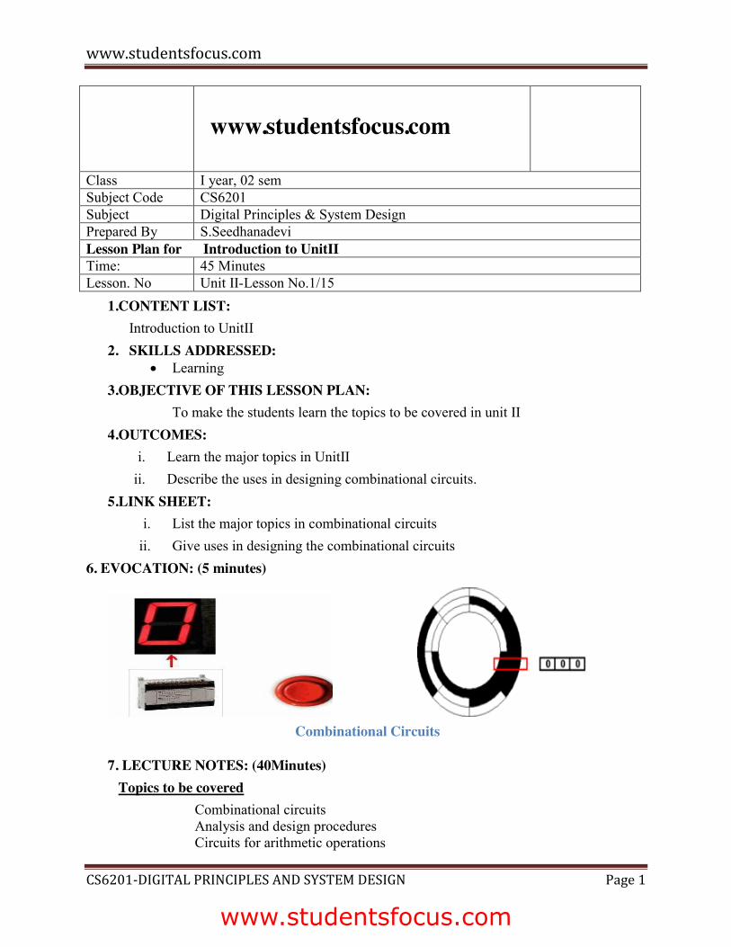
6. EVOCATION: (5 minutes)
Combinational Circuits
7. LECTURE NOTES: (40Minutes) Topics to be covered
Combinational circuits Analysis and design procedures Circuits for arithmetic operations
www.studentsfocus.com
www.studentsfocus.com
www.studentsfocus.com
CS6201-DIGITAL PRINCIPLES AND SYSTEM DESIGN Page 2
Code conversion Decoders Encoders Multiplexers Demultiplexers HDL for combinational circuits
Uses in designing the logic circuits Combinational circuits
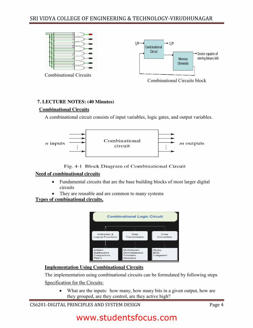
A combinational circuit consists of input variables, logic gates, and output variables.
Analysis and design procedure Used to derive the truthtable and Boolean expression to design various digital logic circuits
Circuits for arithmetic operations Half adder, Full adder, Binary adder, Binary adder/ subtractor, Half subtractor, Full subtractor
Decoders The decoder is called n-to-m-line decoder, where m≤2n .The decoder is also used in conjunction with other code converters such as a BCD-to-seven_segment decoder.
Encoders An encoder is the inverse operation of a decoder. Used in designing the various complex digital circuits.
Multiplexers Multiplexer circuits can be combined with common selection inputs to provide multiple-bit selection logic.
Demultiplexers A decoder with an enable input is referred to as a decoder/demultiplexer.
HDL for combinational circuits 1.Gate-level modeling 2.Dataflow modeling
3.Behavioral modeling 8. TEXT BOOKS:
Sanjay Kumar Suman, L.Bhagyalakshmi, S.Porselvi, “Digital Principles And System Design”,Vijay Nicole Pubilcations
9. APPLICATIONS x Fundamental circuits that are the base building blocks of most larger digital
circuits
www.studentsfocus.com
www.studentsfocus.com
CS6201-DIGITAL PRINCIPLES AND SYSTEM DESIGN Page 3
x They are reusable and are common to many systems
Class I year, 02 sem Subject Code CS6201 Subject Digital Principles & System Design Prepared By S.Seedhanadevi Lesson Plan for Combinational circuits. Time: 45 Minutes Lesson. No Unit II-Lesson No.2/15
1.CONTENT LIST: Combinational circuits.
2. SKILLS ADDRESSED: x Understanding x Learning x Remembering
3. OBJECTIVE OF THIS LESSON PLAN: To make the students learn the meaning of combinational circuits and their implementation.
4.OUTCOMES: i. Learn the meaning of combinational circuits
ii. Describe the implementation of logic circuits by combinational circuits. 5.LINK SHEET:
i. Define combinational circuits with neat block diagram. ii. Give the need of combinational circuits.
iii. List the types of combinational circuits. iv. Explain the implementation using combinational circuits
6.EVOCATION: (5 Minutes)
www.studentsfocus.com
www.studentsfocus.com
www.studentsfocus.com
SRI VIDYA COLLEGE OF ENGINEERING & TECHNOLOGY-VIRUDHUNAGAR
CS6201-DIGITAL PRINCIPLES AND SYSTEM DESIGN Page 4
A combinational circuit consists of input variables, logic gates, and output variables.
Need of combinational circuits
x Fundamental circuits that are the base building blocks of most larger digital circuits
x They are reusable and are common to many systems Types of combinational circuits.
Implementation Using Combinational Circuits The implementation using combinational circuits can be formulated by following steps Specification for the Circuits:
x What are the inputs: how many, how many bits in a given output, how are they grouped, are they control, are they active high?
www.studentsfocus.com
SRI VIDYA COLLEGE OF ENGINEERING & TECHNOLOGY-VIRUDHUNAGAR
CS6201-DIGITAL PRINCIPLES AND SYSTEM DESIGN Page 5
x What are the outputs: how many and how many bits in an each, active high, active low, tristate output?
x The functional operation that takes place in the chip, i.e., for given inputs what will appear on the outputs.
Convert the specifications into a variety forms for optimal implementation. ¾ Possible forms ¾ Truth Tables ¾ Expressions ¾ K-maps ¾ Binary Decision Diagrams
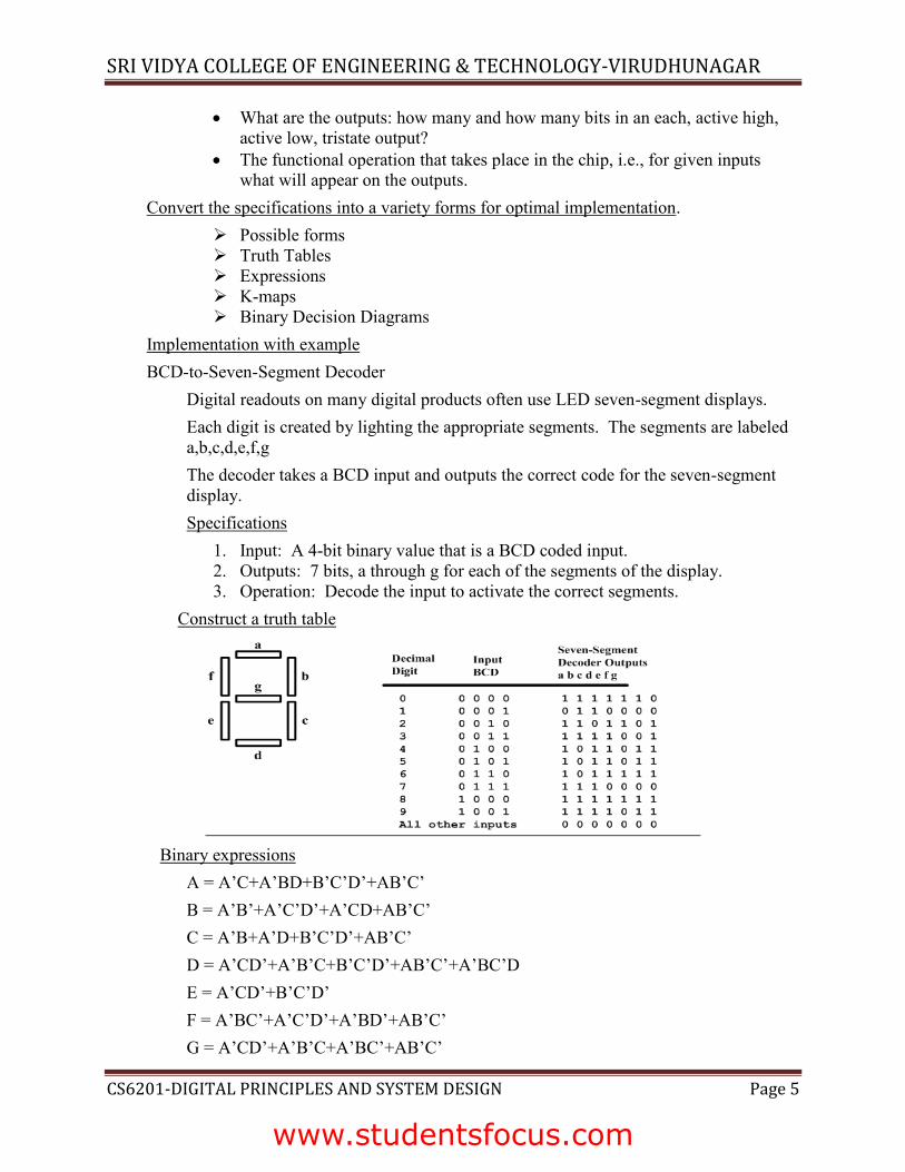
Implementation with example BCD-to-Seven-Segment Decoder
Digital readouts on many digital products often use LED seven-segment displays. Each digit is created by lighting the appropriate segments. The segments are labeled a,b,c,d,e,f,g The decoder takes a BCD input and outputs the correct code for the seven-segment display. Specifications
1. Input: A 4-bit binary value that is a BCD coded input. 2. Outputs: 7 bits, a through g for each of the segments of the display. 3. Operation: Decode the input to activate the correct segments.
Construct a truth table
Binary expressions
A = A’C+A’BD+B’C’D’+AB’C’ B = A’B’+A’C’D’+A’CD+AB’C’ C = A’B+A’D+B’C’D’+AB’C’ D = A’CD’+A’B’C+B’C’D’+AB’C’+A’BC’D E = A’CD’+B’C’D’ F = A’BC’+A’C’D’+A’BD’+AB’C’ G = A’CD’+A’B’C+A’BC’+AB’C’
www.studentsfocus.com
SRI VIDYA COLLEGE OF ENGINEERING & TECHNOLOGY-VIRUDHUNAGAR
CS6201-DIGITAL PRINCIPLES AND SYSTEM DESIGN Page 6
8.TEXT BOOKS: Sanjay Kumar Suman, L.Bhagyalakshmi, S.Porselvi, “Digital Principles And System Design”,Vijay Nicole Pubilcations
9.APPLICATIONS x Fundamental circuits that are the base building blocks of most larger digital
circuits x They are reusable and are common to many systems
Sri Vidya College of Engineering and Technology Department of Information Technology
Class I year, 02 sem Subject Code CS6201 Subject Digital Principles & System Design Prepared By S.Seedhanadevi Lesson Plan for Analysis and design procedures Time: 45 Minutes Lesson. No Unit II-Lesson No.3/15
1.CONTENT LIST: Analysis and design procedures
2. SKILLS ADDRESSED: x Understanding x Applying x Remembering
3. OBJECTIVE OF THIS LESSON PLAN: To make the students apply the steps of implementation in analyzing combinational circuits.
4.OUTCOMES: i. Understand the analysis procedure of combinational circuits
ii. Illustrate the procedure with an example 5.LINK SHEET:
i. Discuss the analysis procedure with major steps. ii. Give an example to illustrate the analysis procedure of combinational circuits.
iii. Derive the truth table and binary expression using the analysis procedure. 6.EVOCATION: (5 Minutes)
www.studentsfocus.com
SRI VIDYA COLLEGE OF ENGINEERING & TECHNOLOGY-VIRUDHUNAGAR
CS6201-DIGITAL PRINCIPLES AND SYSTEM DESIGN Page 7
logic circuit analyzer 1
7. LECTURE NOTES: (40 Minutes)
Analysis Procedure 1. The analysis for a combinational circuit consists of determining the function that
the circuit implements. 2. The analysis starts with a given logic circuit diagram and culminates with a set of
Boolean functions or a truth table, together with a possible explanation of the operation of the circuit.
3. If the logic diagram to be analyzed is accompanied by a recognizable function name or a statement of what the diagram is assumed to accomplish, then the analysis problem reduces to a verification of the stated function.
Steps of analysis procedure x Label all gate outputs that are a function only of input variables or their complements
with arbitrary symbols. Determine the Boolean functions for each gate output. x Label the gates that are a function of input variables and previously labeled gates with
different arbitrary symbols. Find the Boolean functions for the outputs of these gates. x Repeat the process outlined in step 2 until the outputs of the circuit are obtained in
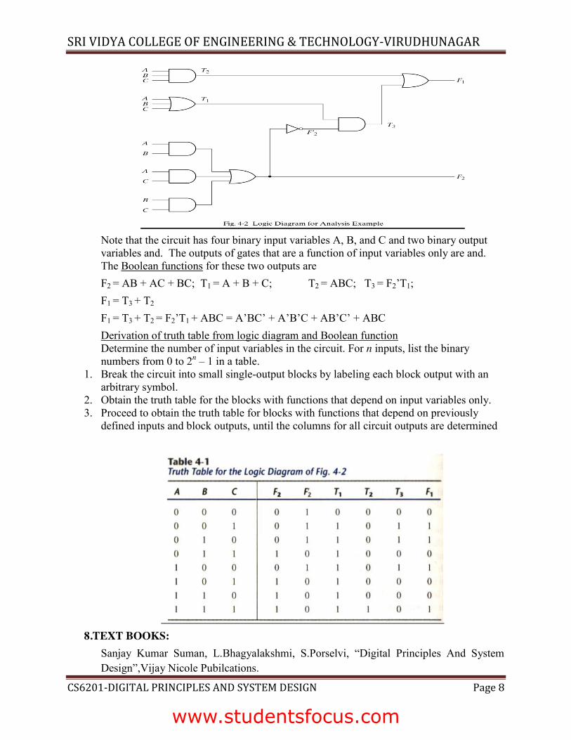
terms of the input variables. Illustration with an example F2 = AB + AC + BC; T1 = A + B + C; T2 = ABC; T3 = F2’T1; F1 = T3 + T2 F1 = T3 + T2 = F2’T1 + ABC = A’BC’ + A’B’C + AB’C’ + ABC
www.studentsfocus.com
SRI VIDYA COLLEGE OF ENGINEERING & TECHNOLOGY-VIRUDHUNAGAR
CS6201-DIGITAL PRINCIPLES AND SYSTEM DESIGN Page 8
Note that the circuit has four binary input variables A, B, and C and two binary output variables and. The outputs of gates that are a function of input variables only are and. The Boolean functions for these two outputs are F2 = AB + AC + BC; T1 = A + B + C; T2 = ABC; T3 = F2’T1; F1 = T3 + T2 F1 = T3 + T2 = F2’T1 + ABC = A’BC’ + A’B’C + AB’C’ + ABC Derivation of truth table from logic diagram and Boolean function Determine the number of input variables in the circuit. For n inputs, list the binary numbers from 0 to 2n – 1 in a table.
1. Break the circuit into small single-output blocks by labeling each block output with an arbitrary symbol.
2. Obtain the truth table for the blocks with functions that depend on input variables only. 3. Proceed to obtain the truth table for blocks with functions that depend on previously
defined inputs and block outputs, until the columns for all circuit outputs are determined
8.TEXT BOOKS:
Sanjay Kumar Suman, L.Bhagyalakshmi, S.Porselvi, “Digital Principles And System Design”,Vijay Nicole Pubilcations.
www.studentsfocus.com
SRI VIDYA COLLEGE OF ENGINEERING & TECHNOLOGY-VIRUDHUNAGAR
CS6201-DIGITAL PRINCIPLES AND SYSTEM DESIGN Page 9
9.APPLICATIONS They are used as building blocks for various intermediate inputs and outputs and thereby
applying it in design of various digital circuits.
Sri Vidya College of Engineering and Technology Department of Information Technology
Class I year, 02 sem Subject Code CS6201 Subject Digital Principles & System Design Prepared By S.Seedhanadevi Lesson Plan for Analysis and design procedures Time: 45 Minutes Lesson. No Unit II-Lesson No.4/15
1.CONTENT LIST: Analysis and design procedures
2. SKILLS ADDRESSED: x Applying x understanding
3. OBJECTIVE OF THIS LESSON PLAN: To make the students apply the steps of implementation in designing the digital logic circuits.
www.studentsfocus.com
SRI VIDYA COLLEGE OF ENGINEERING & TECHNOLOGY-VIRUDHUNAGAR
CS6201-DIGITAL PRINCIPLES AND SYSTEM DESIGN Page 10
4.OUTCOMES: i. Understand the design procedure of combinational circuits
ii. Illustrate the procedure with an example 5.LINK SHEET:
i. Discuss the design procedure with major steps. ii. Give an example to illustrate the design procedure of combinational circuits.
iii. Design the logic circuit based on the steps of design procedure.
6.EVOCATION: (5 Minutes)
Analogy for combinational circuits 1
7. LECTURE NOTES: (40 Minutes) Design Procedure
The design for a combinational circuit consists of determining the function that the implement the circuits.
Steps of analysis procedure x Derivation of truth table x K map and Boolean expression x Circuit implementation Illustration with an example Code-Conversion example, first, we can list the relation of the BCD and Excess-3 codes in the truth table. Derivation of truth table
www.studentsfocus.com
SRI VIDYA COLLEGE OF ENGINEERING & TECHNOLOGY-VIRUDHUNAGAR
CS6201-DIGITAL PRINCIPLES AND SYSTEM DESIGN Page 11
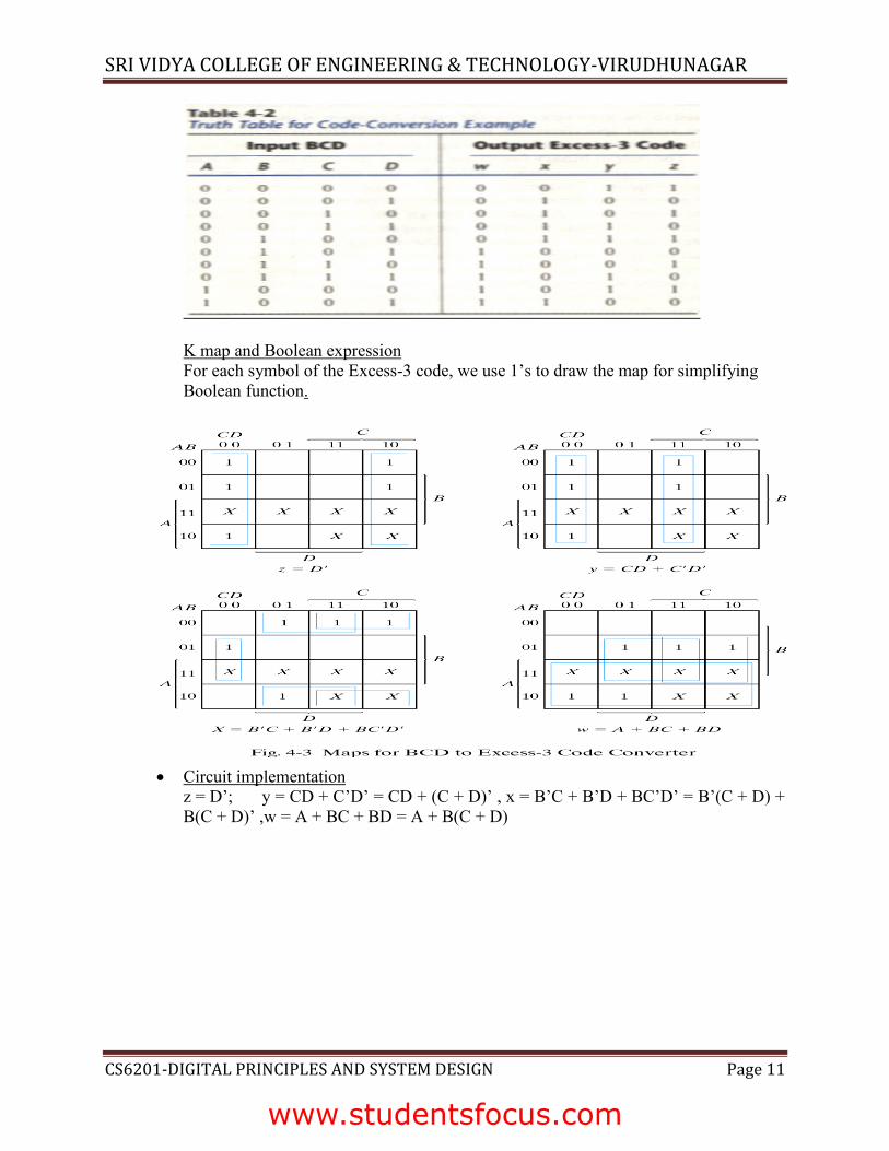
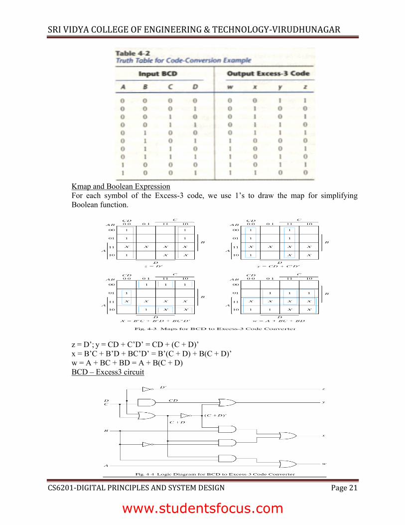
K map and Boolean expression For each symbol of the Excess-3 code, we use 1’s to draw the map for simplifying Boolean function.
x Circuit implementation
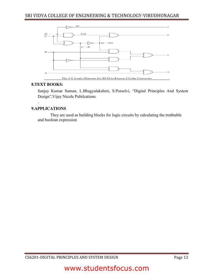
z = D’; y = CD + C’D’ = CD + (C + D)’ , x = B’C + B’D + BC’D’ = B’(C + D) + B(C + D)’ ,w = A + BC + BD = A + B(C + D)
www.studentsfocus.com
SRI VIDYA COLLEGE OF ENGINEERING & TECHNOLOGY-VIRUDHUNAGAR
CS6201-DIGITAL PRINCIPLES AND SYSTEM DESIGN Page 12
8.TEXT BOOKS:
Sanjay Kumar Suman, L.Bhagyalakshmi, S.Porselvi, “Digital Principles And System Design”,Vijay Nicole Pubilcations. .
9.APPLICATIONS They are used as building blocks for logic circuits by calculating the truthtable
and boolean expression
www.studentsfocus.com
SRI VIDYA COLLEGE OF ENGINEERING & TECHNOLOGY-VIRUDHUNAGAR
CS6201-DIGITAL PRINCIPLES AND SYSTEM DESIGN Page 13
Sri Vidya College of Engineering and Technology Department of Information Technology
Class I year, 02 sem Subject Code CS6201 Subject Digital Principles & System Design Prepared By S.Seedhanadevi Lesson Plan for Circuits for arithmetic operations Time: 45 Minutes Lesson. No Unit II-Lesson No.5/15
1.CONTENT LIST: Circuits for arithmetic operations
2. SKILLS ADDRESSED: x Remembering x Learning x Classifying
3. OBJECTIVE OF THIS LESSON PLAN: To make the students know the basic concept of arithmetic circuits
4.OUTCOMES: i. Describe the various classification of arithmetic circuits
ii. Deduce the basic concept of arithmetic circuits 5.LINK SHEET:
i. List the types of arithmetic circuits. ii. Define all the arithmetic circuits which help in designing combinational circuits.
iii. What is the need for using arithmetic circuits in designing combinational circuits? iv. Design half adder circuit and full adder circuit using truth table and Boolean
expression 6. EVOCATION: (5 Minutes)
Fulladder-redstone scenario
7. LECTURE NOTES: (40 Minutes) Types of arithmetic circuits
www.studentsfocus.com
SRI VIDYA COLLEGE OF ENGINEERING & TECHNOLOGY-VIRUDHUNAGAR
CS6201-DIGITAL PRINCIPLES AND SYSTEM DESIGN Page 14
A combinational circuit that performs the addition of two bits is called a half adder. Full Adder:
One that performs the addition of three bits(two significant bits and a previous carry) is a full adder.
Binary Adder: This is also called Ripple Carry Adder ,because of the construction with full adders are connected in cascade.
Binary subtractor: M = 1Æsubtractor ; M = 0Æadder
Overflow is a problem in digital computers because the number of bits that hold the number is finite and a result that contains n+1 bits cannot be accommodated.
Binary multiplier: Usually there are more bits in the partial products and it is necessary to use full adders to produce the sum of the partial products.
Need for using arithmetic circuits in designing combinational circuits: � reduce cost
¾ reduce number of gates (for SSI circuits) ¾ reduce IC packages (for complex circuits)
� (ii) increase speed � (iii) design simplicity (reuse blocks where possible)
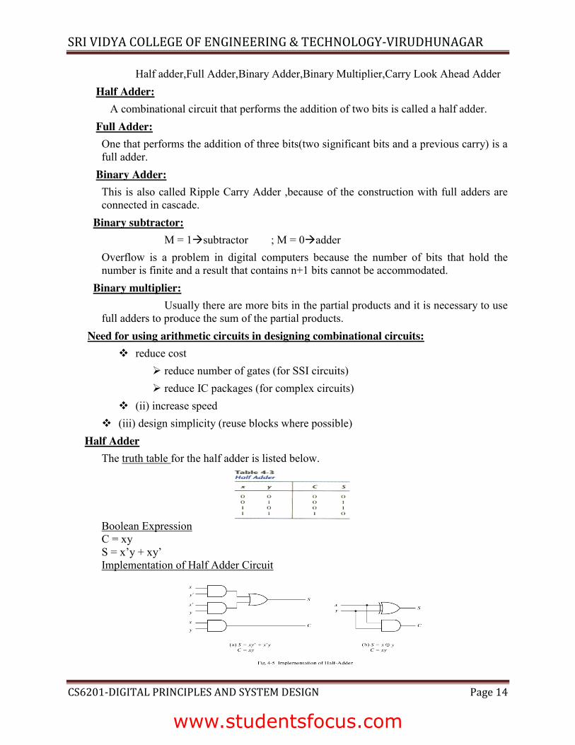
Half Adder The truth table for the half adder is listed below.
Boolean Expression C = xy S = x’y + xy’ Implementation of Half Adder Circuit
www.studentsfocus.com
SRI VIDYA COLLEGE OF ENGINEERING & TECHNOLOGY-VIRUDHUNAGAR
CS6201-DIGITAL PRINCIPLES AND SYSTEM DESIGN Page 15
Full Adder One that performs the addition of three bits (two significant bits and a previous carry) is a full adder.
Truth Table
Boolean expression using K map
S = x’y’z + x’yz’ + xy’z’ + xyz C = xy + xz + yz Implementation of Full adder circuit
8.TEXT BOOKS: Sanjay Kumar Suman, L.Bhagyalakshmi, S.Porselvi, “Digital Principles And System Design”,Vijay Nicole Pubilcations. .
9.APPLICATIONS The arithmetic circuits are used to reduce the cost, increase the speed and design very complex digital circuits with ease
www.studentsfocus.com
SRI VIDYA COLLEGE OF ENGINEERING & TECHNOLOGY-VIRUDHUNAGAR
CS6201-DIGITAL PRINCIPLES AND SYSTEM DESIGN Page 16
Sri Vidya College of Engineering and Technology Department of Information Technology
Class I year, 02 sem Subject Code CS6201 Subject Digital Principles & System Design Prepared By S.Seedhanadevi Lesson Plan for Circuits for arithmetic operations Time: 45 Minutes Lesson. No Unit II-Lesson No.6/15
1.CONTENT LIST: Circuits for arithmetic operations
2. SKILLS ADDRESSED: x Remembering x Learning x Analyzing
3. OBJECTIVE OF THIS LESSON PLAN: To make the students know the basic operation of all the arithmetic circuits
4.OUTCOMES: i. Discuss the operation of all the arithmetic circuits
ii. Design logic diagram by the steps used in the basic mode of operation 5.LINK SHEET:
i. Explain the operation of individual arithmetic circuits ii. What are the modes used in designing arithmetic circuits?
iii. Design the binary adder; carry look adder, Binary Multiplier and Binary Subtractor circuit using the basic mode of operation.
6. EVOCATION: (5 Minutes)
binary adder-subtractor
Gates used in arithmetic circuits
7. LECTURE NOTES: (40 Minutes)
www.studentsfocus.com
SRI VIDYA COLLEGE OF ENGINEERING & TECHNOLOGY-VIRUDHUNAGAR
CS6201-DIGITAL PRINCIPLES AND SYSTEM DESIGN Page 17
Major Steps: x Truthtable x Boolean expression using Kmap x Logic circuit
Binary adder This is also called Ripple Carry Adder, because of the construction with full adders are connected in cascade.
Truth Table
Implementation of Binary adder circuit
Carry Look Ahead Adder The most widely used technique employs the principle of carry look-ahead to improve the speed of the algorithm. Boolean expression Pi = Ai ⊕ Bi steady state value Gi = AiBi steady state value Output sum and carry Si = Pi ⊕ Ci Ci+1 = Gi + PiCi Gi : carry generate Pi : carry propagate C0 = input carry C1 = G0 + P0C0 C2 = G1 + P1C1 = G1 + P1G0 + P1P0C0 C3 = G2 + P2C2 = G2 + P2G1 + P2P1G0 + P2P1P0C0 Implementation of Carry Look ahead adder circuit
www.studentsfocus.com
SRI VIDYA COLLEGE OF ENGINEERING & TECHNOLOGY-VIRUDHUNAGAR
CS6201-DIGITAL PRINCIPLES AND SYSTEM DESIGN Page 18
Binary subtractor: M = 1Æsubtractor ; M = 0Æadder
Overflow is a problem in digital computers because the number of bits that hold the number is finite and a result that contains n+1 bits cannot be accommodated. Implementation of Binary Subtractor circuit
Binary multiplier: Usually there are more bits in the partial products and it is necessary to use full adders to produce the sum of the partial products. For J multiplier bits and K multiplicand bits we need (J X K) AND gates and (J − 1) K-bit adders to produce a product of J+K bits. K=4 and J=3, we need 12 AND gates and two 4-bit adders. Implementation of 4-bit by 3-bit binary multiplier circuit
8.TEXT BOOKS:
www.studentsfocus.com
SRI VIDYA COLLEGE OF ENGINEERING & TECHNOLOGY-VIRUDHUNAGAR
CS6201-DIGITAL PRINCIPLES AND SYSTEM DESIGN Page 19
Sanjay Kumar Suman, L.Bhagyalakshmi, S.Porselvi, “Digital Principles And System Design”,Vijay Nicole Pubilcations.
9.APPLICATIONS x They present special design challenges, because there are simply too many inputs
to list all possible combinations in a truth table. x In applying this method, bus-wide operations are broken into simpler bit-by-bit
operations that are more easily defined by truth-tables, and more tractable to familiar design techniques
Sri Vidya College of Engineering and Technology Department of Information Technology
Class I year, 02 sem Subject Code CS6201 Subject Digital Principles & System Design Prepared By S.Seedhanadevi Lesson Plan for Code conversion Time: 45 Minutes Lesson. No Unit II-Lesson No.7/15
1.CONTENT LIST: Code conversion
2. SKILLS ADDRESSED: x Remembering x Applying
3. OBJECTIVE OF THIS LESSON PLAN: To make the students know the basic concept of code conversion and to use their principle in various code conversion circuits.
4.OUTCOMES: i. Deduce the Principle of code conversion
ii. Describe the various code conversion methods using the principle. 5.LINK SHEET:
i. What is the principle of code conversion? ii. List the types of code conversion circuits
iii. Design any one of the code conversion circuit by the principle used. 6. EVOCATION: (5 Minutes)
www.studentsfocus.com
SRI VIDYA COLLEGE OF ENGINEERING & TECHNOLOGY-VIRUDHUNAGAR
CS6201-DIGITAL PRINCIPLES AND SYSTEM DESIGN Page 20
7. LECTURE NOTES: (40 Minutes) Code Conversion
Conversion of signals, or groups of signals, in one code into corresponding signals, or groups of signals, in another code.
Principle of Code Conversion A process for converting a code of some predetermined bit structure, such as 5, 7, or 14 bits per character interval, to another code with the same or a different number of bits per character interval. Types of codeconversion
x BCD to Gray code. and viceversa. x BCD to excess3 code and viceversa. x Binary to gray code and viceversa x
Implementation of code conversion circuit BCD and Excess-3 codes Truth Table
Code Conversion Examples
www.studentsfocus.com
SRI VIDYA COLLEGE OF ENGINEERING & TECHNOLOGY-VIRUDHUNAGAR
CS6201-DIGITAL PRINCIPLES AND SYSTEM DESIGN Page 21
Kmap and Boolean Expression For each symbol of the Excess-3 code, we use 1’s to draw the map for simplifying Boolean function.
z = D’; y = CD + C’D’ = CD + (C + D)’ x = B’C + B’D + BC’D’ = B’(C + D) + B(C + D)’ w = A + BC + BD = A + B(C + D) BCD – Excess3 circuit
www.studentsfocus.com
SRI VIDYA COLLEGE OF ENGINEERING & TECHNOLOGY-VIRUDHUNAGAR
CS6201-DIGITAL PRINCIPLES AND SYSTEM DESIGN Page 22
8.TEXT BOOKS:
Sanjay Kumar Suman, L.Bhagyalakshmi, S.Porselvi, “Digital Principles And System Design”,Vijay Nicole Pubilcations.
9.APPLICATIONS The principle is applied in digital speakers, sound cards and stereo to 3D displays
Sri Vidya College of Engineering and Technology Department of Information Technology
Class I year, 02 sem Subject Code CS6201 Subject Digital Principles & System Design Prepared By S.Seedhanadevi Lesson Plan for Decoders Time: 45 Minutes Lesson. No Unit II-Lesson No.8/15
1.CONTENT LIST: Decoders
2. SKILLS ADDRESSED: x Remembering x Understanding
3. OBJECTIVE OF THIS LESSON PLAN: To make the students know the basic concept of decoders and implement their types using the basic logic
4.OUTCOMES: i. Describe the basic concept of decoders
ii. Explain the types of decoders and implement their design using the basic logic 5.LINK SHEET:
i. What is the decoder?
www.studentsfocus.com
SRI VIDYA COLLEGE OF ENGINEERING & TECHNOLOGY-VIRUDHUNAGAR
CS6201-DIGITAL PRINCIPLES AND SYSTEM DESIGN Page 23
ii. List the types of decoder. iii. Implement any one of the decoder circuit with necessary diagrams wherever
necessary. 6. EVOCATION: (5 Minutes)
7. LECTURE NOTES: (40 Minutes) Decoder ¾ The decoder is called n-to-m-line decoder, where m≤2n the decoder is also used in
conjunction with other code converters such as a BCD-to-seven segment decoder. ¾ 3-to-8 line decoder: For each possible input combination, there are seven outputs
that are equal to 0 and only one that is equal to 1. ¾ Some decoders are constructed with NAND gates, it becomes more economical to
generate the decoder minters in their complemented form. ¾ As indicated by the truth table, only one output can be equal to 0 at any given
time, all other outputs are equal to 1. Types of decoder
x 2to4 decoder x 3to8decoder x 4to16decoder and so on.
Implementation of decoder circuit 3 to 8 decoder
Decoder Examples
www.studentsfocus.com
SRI VIDYA COLLEGE OF ENGINEERING & TECHNOLOGY-VIRUDHUNAGAR
CS6201-DIGITAL PRINCIPLES AND SYSTEM DESIGN Page 24
2 to 4 decoder
8.TEXT BOOKS:
www.studentsfocus.com
SRI VIDYA COLLEGE OF ENGINEERING & TECHNOLOGY-VIRUDHUNAGAR
CS6201-DIGITAL PRINCIPLES AND SYSTEM DESIGN Page 25
Sanjay Kumar Suman, L.Bhagyalakshmi, S.Porselvi, “Digital Principles And System Design”,Vijay Nicole Pubilcations.
9.APPLICATIONS Decoders are used to analyze data streams for a certain data code and give an output if the data is present like an address to a peripheral unit that needs service.
Sri Vidya College of Engineering and Technology Department of Information Technology
Class I year, 02 sem Subject Code CS6201 Subject Digital Principles & System Design Prepared By S.Seedhanadevi Lesson Plan for Encoders Time: 45 Minutes Lesson. No Unit II-Lesson No.9/15
1.CONTENT LIST: Encoders
2. SKILLS ADDRESSED: x Remembering x Learning
3. OBJECTIVE OF THIS LESSON PLAN: To make the students know the basic concept of encoders and implement their types using the basic logic
4.OUTCOMES: i. Describe the basic concept of encoders
ii. Explain the types of encoders and implement their design using the basic logic 5.LINK SHEET:
i. What is the encoder?
www.studentsfocus.com
SRI VIDYA COLLEGE OF ENGINEERING & TECHNOLOGY-VIRUDHUNAGAR
CS6201-DIGITAL PRINCIPLES AND SYSTEM DESIGN Page 26
ii. Implement any one of the encoder circuit with necessary diagrams wherever necessary.
iii. List the types of encoder 6. EVOCATION: (5 Minutes)
7. LECTURE NOTES: (40 Minutes) Encoder ¾ An encoder is the inverse operation of a decoder (ie) contains m inputs and
convert it into to n outputs ¾ If two inputs are active simultaneously, the output produces an undefined
combination. We can establish an input priority to ensure that only one input is encoded.
¾ Another ambiguity in the octal-to-binary encoder is that an output with all 0’s is generated when all the inputs are 0; the output is the same as when D0 is equal to 1.
Types of Encoder x 4to2 encoder,8to3 encoder,16to4 encoder, Priority encoder and so on
SRI VIDYA COLLEGE OF ENGINEERING & TECHNOLOGY-VIRUDHUNAGAR
CS6201-DIGITAL PRINCIPLES AND SYSTEM DESIGN Page 27
V=0Æno valid inputs, V=1Ævalid inputs
o X’s in output columns represent don’t-care conditions. X’s in the input columns are useful for representing a truth table in condensed form. Instead of listing all 16 minterms of four variables.
x = D2 + D3 , y = D3 + D1D’2 , V = D0 + D1 + D2 + D
www.studentsfocus.com
SRI VIDYA COLLEGE OF ENGINEERING & TECHNOLOGY-VIRUDHUNAGAR
CS6201-DIGITAL PRINCIPLES AND SYSTEM DESIGN Page 28
8.TEXT BOOKS: Sanjay Kumar Suman, L.Bhagyalakshmi, S.Porselvi, “Digital Principles And System Design”,Vijay Nicole Pubilcations. .
9.APPLICATIONS An encoder is a device, circuit, transducer, software program, algorithm or person that converts information from one format or code to another, for the purposes of standardization, speed, secrecy, security or compressions..
Sri Vidya College of Engineering and Technology Department of Information Technology
Class I year, 02 sem Subject Code CS6201 Subject Digital Principles & System Design Prepared By S.Seedhanadevi Lesson Plan for Multiplexers Time: 45 Minutes Lesson. No Unit II-Lesson No.10/15
1.CONTENT LIST: Multiplexers
2. SKILLS ADDRESSED: x Remembering x Understanding
3. OBJECTIVE OF THIS LESSON PLAN: To make the students know the basic concept of Multiplexers and implement their types using the basic logic
4.OUTCOMES:
www.studentsfocus.com
SRI VIDYA COLLEGE OF ENGINEERING & TECHNOLOGY-VIRUDHUNAGAR
CS6201-DIGITAL PRINCIPLES AND SYSTEM DESIGN Page 29
i. Describe the basic concept of Multiplexers ii. Explain the types of Multiplexers and implement their design using the basic logic
5.LINK SHEET: i. What is the Multiplexers and write the other name for Multiplexers?
ii. Implement any one of the Multiplexers circuit with necessary diagrams wherever necessary.
iii. List the types of Multiplexers iv. Implement the Boolean function using any one of the multiplexer circuit
6. EVOCATION: (5 Minutes)
7. LECTURE NOTES: (40 Minutes) Multiplexer ¾ In electronics, a multiplexer (or mux) is a device that selects one of several
analog or digital input signals and forwards the selected input into a single line. ¾ A multiplexer of 2n inputs has n select lines, which are used to select which input
line to send to the output. ¾ Multiplexers are mainly used to increase the amount of data that can be sent over
the network within a certain amount of time and bandwidth.
Multiplexing examples
www.studentsfocus.com
SRI VIDYA COLLEGE OF ENGINEERING & TECHNOLOGY-VIRUDHUNAGAR
CS6201-DIGITAL PRINCIPLES AND SYSTEM DESIGN Page 30
¾ A multiplexer is also called a data selector. Types of Muliplexer
x 2 to 1 MUX x 4 to 1 MUX x 16 to 1 MUX and so on
Implementation of MUX circuit 2 to 1 MUX S = 0, Y = I0 Truth TableÆ S Y S = 1, Y = I1 0 I0 Y = S’I0 + SI1 1 I1
4 to 1 MUX
Boolean function implementation
A more efficient method for implementing a Boolean function of n variables with a multiplexer that has n-1 selection inputs.
F(x, y, z) = 6(1,2,6,7)
www.studentsfocus.com
SRI VIDYA COLLEGE OF ENGINEERING & TECHNOLOGY-VIRUDHUNAGAR
CS6201-DIGITAL PRINCIPLES AND SYSTEM DESIGN Page 31
8.TEXT BOOKS: Sanjay Kumar Suman, L.Bhagyalakshmi, S.Porselvi, “Digital Principles And System Design”,Vijay Nicole Pubilcations.
9.APPLICATIONS Mux is used in telephony, telegraphy, digital broadcasting and analog broadcasting. An electronic multiplexer makes it possible for several signals to share one device or resource, for example one A/D converter or one communication line, instead of having one device per input signal.
Sri Vidya College of Engineering and Technology Department of Information Technology
Class I year, 02 sem Subject Code CS6201 Subject Digital Principles & System Design Prepared By S.Seedhanadevi Lesson Plan for Demultiplexers Time: 45 Minutes Lesson. No Unit II-Lesson No.11/15
1.CONTENT LIST: Demultiplexers
2. SKILLS ADDRESSED: x Remembering x Understanding
www.studentsfocus.com
SRI VIDYA COLLEGE OF ENGINEERING & TECHNOLOGY-VIRUDHUNAGAR
CS6201-DIGITAL PRINCIPLES AND SYSTEM DESIGN Page 32
3. OBJECTIVE OF THIS LESSON PLAN: To make the students know the basic concept of Demultiplexers and implement their types using the basic logic
4.OUTCOMES: i. Describe the basic concept of Demultiplexers
ii. Explain the types of Demultiplexers and implement their design using the basic logic
5.LINK SHEET: i. What is the Demultiplexers and write the other name for Demultiplexers?
ii. Implement any one of the Demultiplexers circuit with necessary diagrams wherever necessary.
iii. List the types of Demultiplexers 6. EVOCATION: (5 Minutes)
7. LECTURE NOTES: (40 Minutes) Demultiplexer ¾ Demultiplexer (or demux) is a device taking a single input signal and selecting
one of many data-output-lines, which is connected to the single ¾ It is otherwise known as data distributor. ¾ A decoder with an enable input is referred to as a decoder/demultiplexer. ¾ The truth table of demultiplexer is the same with decoder.
Types of Demuliplexer
x 1 to 2 DEMUX,1 to 4 DEMUX,1 to 16 DeMUX and so on
Demultiplexing examples
www.studentsfocus.com
SRI VIDYA COLLEGE OF ENGINEERING & TECHNOLOGY-VIRUDHUNAGAR
CS6201-DIGITAL PRINCIPLES AND SYSTEM DESIGN Page 33
Implementation of DEMUX circuit 1-to-4 De-multiplexer
The Boolean expression for this 1-to-4 Demultiplexer above with outputs A to D and data select lines a, b is given as: F = ab A + abB + abC + abD
8.TEXT BOOKS: Sanjay Kumar Suman, L.Bhagyalakshmi, S.Porselvi, “Digital Principles And System Design”,Vijay Nicole Pubilcations.
9.APPLICATIONS Demultiplexer is used to connect a single source to multiple destinations. It is used in ALU circuit. The second use of the Demultiplexer is the reconstruction of Parallel Data from the incoming serial data stream.
Sri Vidya College of Engineering and Technology Department of Information Technology
Class I year, 02 sem Subject Code CS6201 Subject Digital Principles & System Design Prepared By S.Seedhanadevi Lesson Plan for Introduction to Hardware Description Language (HDL) Time: 45 Minutes Lesson. No Unit II-Lesson No.12/15
1.CONTENT LIST: Introduction to Hardware Description Language (HDL)
2. SKILLS ADDRESSED:
Addressing Input Selected b a
0 0 A 0 1 B 1 0 C 1 1 D
www.studentsfocus.com
SRI VIDYA COLLEGE OF ENGINEERING & TECHNOLOGY-VIRUDHUNAGAR
CS6201-DIGITAL PRINCIPLES AND SYSTEM DESIGN Page 34
x Remembering x Learning
3. OBJECTIVE OF THIS LESSON PLAN: To make the students know the basics of HDL and know their advantages in hardware implementation
4.OUTCOMES: i. Describe the basic concept of HDL
ii. Explain design methodologies using HDL 5.LINK SHEET:
i. What is HDL ii. Write the HDL coding for the circuit given
iii. Evaluate in brief the modeling techniques of HDL 6. EVOCATION: (5 Minutes)
7. LECTURE NOTES: (40 Minutes) HDL ¾ In electronics, a Hardware Description Language or HDL is any language from
a class of computer languages, specification languages, or modeling languages for formal description and design of electronic circuits, and most-commonly, digital logic.
¾ It can describe the circuit's operation, its design and organization, and tests to verify its operation by means of simulation.
HDL coding for given circuit
www.studentsfocus.com
SRI VIDYA COLLEGE OF ENGINEERING & TECHNOLOGY-VIRUDHUNAGAR
CS6201-DIGITAL PRINCIPLES AND SYSTEM DESIGN Page 35
Sanjay Kumar Suman, L.Bhagyalakshmi, S.Porselvi, “Digital Principles And System Design”,Vijay Nicole Pubilcations.
9.APPLICATIONS x Hardware description language enables a precise, formal description of an electronic
circuit that allows for the automated analysis, simulation, and simulated testing of an electronic circuit.
x A hardware description language looks much like a programming language such as C; it is a textual description consisting of expressions and statements.
Sri Vidya College of Engineering and Technology Department of Information Technology
Class I year, 02 sem Subject Code CS6201 Subject Digital Principles & System Design Prepared By S.Seedhanadevi
www.studentsfocus.com
SRI VIDYA COLLEGE OF ENGINEERING & TECHNOLOGY-VIRUDHUNAGAR
CS6201-DIGITAL PRINCIPLES AND SYSTEM DESIGN Page 36
Lesson Plan for HDL for Combinational Circuits Time: 45 Minutes Lesson. No Unit II-Lesson No.13/15
1.CONTENT LIST: HDL for Combinational Circuits
2. SKILLS ADDRESSED: x Remembering x Understanding x Applying
3. OBJECTIVE OF THIS LESSON PLAN: To make the students know the various modeling techniques and their description using HDL
4.OUTCOMES: i. Describe the various types of modeling techniques
ii. Deduce the HDL coding for each modeling techniques 5.LINK SHEET:
i. What is Gate level modeling? ii. What is Behavioral modeling?
iii. Explain Gate level modeling and Behavioral modeling with an example 6. EVOCATION: (5 Minutes)
7. LECTURE NOTES: (40 Minutes) Modelling Techniques A module can be described in any one of the following modeling techniques:
¾ Gate-level modeling uses instantiation of primitive gates and user-defined modules.
¾ Dataflow modeling uses continuous assignment statements with keyword assign.
www.studentsfocus.com
SRI VIDYA COLLEGE OF ENGINEERING & TECHNOLOGY-VIRUDHUNAGAR
CS6201-DIGITAL PRINCIPLES AND SYSTEM DESIGN Page 37
¾ Behavioral modeling uses procedural assignment statements with keyword always.
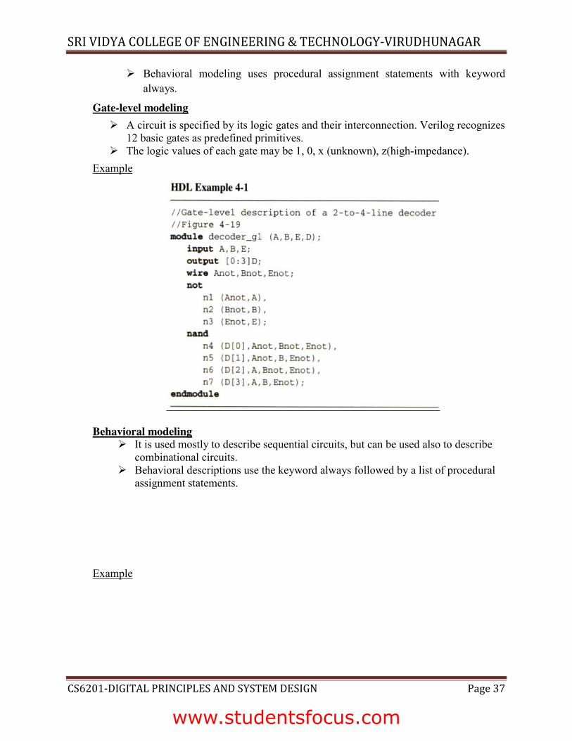
Gate-level modeling ¾ A circuit is specified by its logic gates and their interconnection. Verilog recognizes
12 basic gates as predefined primitives. ¾ The logic values of each gate may be 1, 0, x (unknown), z(high-impedance).
Example
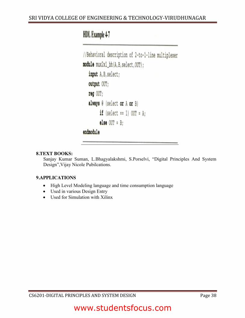
Behavioral modeling ¾ It is used mostly to describe sequential circuits, but can be used also to describe
combinational circuits. ¾ Behavioral descriptions use the keyword always followed by a list of procedural
assignment statements.
Example
www.studentsfocus.com
SRI VIDYA COLLEGE OF ENGINEERING & TECHNOLOGY-VIRUDHUNAGAR
CS6201-DIGITAL PRINCIPLES AND SYSTEM DESIGN Page 38
8.TEXT BOOKS: Sanjay Kumar Suman, L.Bhagyalakshmi, S.Porselvi, “Digital Principles And System Design”,Vijay Nicole Pubilcations.
9.APPLICATIONS x High Level Modeling language and time consumption language x Used in various Design Entry x Used for Simulation with Xilinx
www.studentsfocus.com
SRI VIDYA COLLEGE OF ENGINEERING & TECHNOLOGY-VIRUDHUNAGAR
CS6201-DIGITAL PRINCIPLES AND SYSTEM DESIGN Page 39
Sri Vidya College of Engineering and Technology Department of Information Technology
Class I year, 02 sem Subject Code CS6201 Subject Digital Principles & System Design Prepared By S.Seedhanadevi Lesson Plan for HDL for Combinational Circuits Time: 45 Minutes Lesson. No Unit II-Lesson No.14/15
1.CONTENT LIST: HDL for Combinational Circuits
2. SKILLS ADDRESSED: x Remembering x Understanding x Applying
3. OBJECTIVE OF THIS LESSON PLAN: To make the students know the various design methodologies and their description using HDL
4.OUTCOMES: i. Describe the various design methodologies
ii. Deduce the HDL coding for each design methodologies 5.LINK SHEET:
i. What is Data Flow modeling? ii. What is design methodology for HDL and explain it with an example?
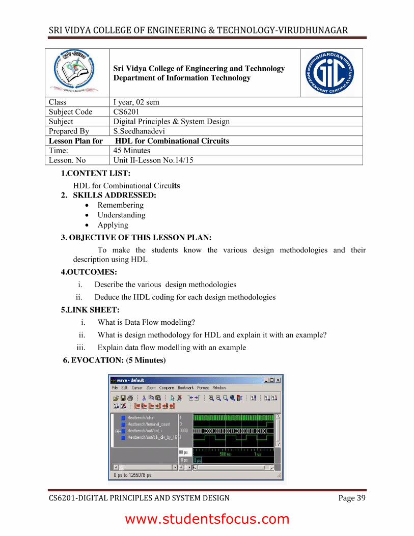
iii. Explain data flow modelling with an example 6. EVOCATION: (5 Minutes)
www.studentsfocus.com
SRI VIDYA COLLEGE OF ENGINEERING & TECHNOLOGY-VIRUDHUNAGAR
CS6201-DIGITAL PRINCIPLES AND SYSTEM DESIGN Page 40
7. LECTURE NOTES: (40 Minutes) Data Flow Modelling
¾ A continuous assignment is a statement that assigns a value to a net. ¾ The data type net is used in Verilog HDL to represent a physical connection
between circuit elements. ¾ A net defines a gate output declared by an output or wire.
Example
Design Methodology and its types
¾ There are two basic types of design methodologies: top-down and bottom-up. ¾ Top-down: the top-level block is defined and then the sub-blocks necessary to
build the top-level block are identified ¾ Bottom-up: the building blocks are first identified and then combined to build the
top-level block. Example
8.TEXT BOOKS:
Sanjay Kumar Suman, L.Bhagyalakshmi, S.Porselvi, “Digital Principles And System Design”,Vijay Nicole Pubilcations.
9.APPLICATIONS x High Level Modeling language and time consumption language x Used in various Design Entry.