XDK110: Getting Started Guide with Extension Bus Cross-Domain Development Kit XDK110 Platform for Application Development XDK110: Extension Bus Guide Document revision 1.0 Document release date 27. February 2018 Workbench version 3.0.0 and above Document number BCDS-XDK110-GUIDE EXTENSION BUS Technical reference code(s) Notes Data in this document is subject to change without notice. Product photos and pictures are for illustration purposes only and may differ from the real product’s appearance. This document is confidential and under NDA inherent with the purchase of an XDK110. Advance information – Subject to change without notice
Transcript
XDK110: Getting Started Guide with Extension BusCross-Domain Development Kit XDK110Platform for Application Development
XDK110: Extension Bus Guide
Document revision 1.0
Document release date 27. February 2018
Workbench version 3.0.0 and above
Document number BCDS-XDK110-GUIDE EXTENSION BUS
Technical reference code(s)
Notes Data in this document is subject to change without notice. Product photos and pictures are for illustration purposes only and may differ from the real product’s appearance.This document is confidential and under NDA inherent with the purchase of an XDK110.Advance information – Subject to change without notice
� | �2 27Extension Bus Guide | XDK110
Table of contents
1. General Description 4
1.1 Introduction to Extension Bus 4...............................................................................................................................
1.2 Connecting the Extension Bus 4.............................................................................................................................
1.3 MCU pins on the Extension Bus 4...........................................................................................................................
3.1 General Introduction 8.............................................................................................................................................
3.2 Pull Up, Pull Down Resistor and Electrical Current Limitation 8.............................................................................
3.3 Configuring a GPIO pin 9........................................................................................................................................
3.5 Writing and reading data from a GPIO pin 11..........................................................................................................
4. Analog to Digital Converter (ADC) 13
4.1 General Introduction 13...........................................................................................................................................
4.2 Configuring the ADC 13...........................................................................................................................................
4.2 Performing a single ADC conversion 14..................................................................................................................
4.3 Performing a scan ADC conversion 15...................................................................................................................
5. Interrupts 17
6. Clock Management 18
7. Timer and Counter 19
7.1 General Introduction 19...........................................................................................................................................
� | �3 27Extension Bus Guide | XDK110
This guide postulates a basic understanding of the XDK and according Workspace. For new users we recommend going through the following guides at xdk.io/guides first:
7.2 Configuring the Timer 20.........................................................................................................................................
7.3 Configuring the Timer for PWM usage 22...............................................................................................................
8. Pulse Counter 24
8.1 General Introduction 24...........................................................................................................................................
8.2 Configuring the Pulse Counter 24..........................................................................................................................
6.1 General Introduction 24...........................................................................................................................................
1. General Description1.1 Introduction to Extension BusThe XDK comes with an interface 26-pin interface for the XDK Gateway, which will be referred to as the extension bus in this document. The extension bus allows access to the XDK's micocontroller unit (MCU) pins and thus attaching external devices such as sensors or actuators to it. All MCU pins are GPIOs and can be configured freely within the limitations of the MCU. This way, developers can use the hardware and software of the XDK for testing out new components with minimal application effort.
The availability and the names of the different MCU pins will be explained in chapter 1.3. For further information on the MCU pin functionality, please refer to the MCU reference manual.
1.2 Connecting the Extension BusConnect the 26-pin cable (included in delivery) to the extension bus board and to the 26-pin connector of the XDK. The extension bus offers a simple way to implement additional functions with external components. It is optimized for the use with breadboards.
1.3 MCU pins on the Extension BusThe extension bus I/O pins are labelled with the respective MCU pin designator. Since all pins of XDK’s MCU are general purpose pins, alternative functionality can be configured for each pin. For example, if a pin is labelled as a Timer, it can also be configured to be used for a pulse counter, and so on. The different functionalities of these pins are described in the data sheet of the EFM32GG390.
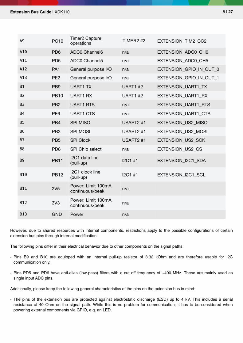
Table 1 describes the selected functionalities for each pin.
Table 1. Pin labelling and configuration of the extension bus
However, due to shared resources with internal components, restrictions apply to the possible configurations of certain extension bus pins through internal modification.
The following pins differ in their electrical behavior due to other components on the signal paths:
• Pins B9 and B10 are equipped with an internal pull-up resistor of 3.32 kOhm and are therefore usable for I2C communication only.
• Pins PD5 and PD6 have anti-alias (low-pass) filters with a cut off frequency of ~400 MHz. These are mainly used as single input ADC pins.
Additionally, please keep the following general characteristics of the pins on the extension bus in mind:
• The pins of the extension bus are protected against electrostatic discharge (ESD) up to 4 kV. This includes a serial resistance of 40 Ohm on the signal path. While this is no problem for communication, it has to be considered when powering external components via GPIO, e.g. an LED.
• Any pin you intend to use will have to be configured accordingly. How to do that will be explained in chapter 3.3. Most of the pins are assigned with default modes and values. For more information, please refer to SDK/xdk110/Platform/BSP/source/BSP_BoardSettings.h and SDK/xdk110/Platform/BSP/source/BSP_BoardExtSettings.h.
• The 2.5 V and 3.3 V power supply pins can provide up to 100 mA supply current, please note that these limitations apply to the maximal peak current, too. By default, the 3V3 supply pin is in a disabled state. For your application, please use the function Board_EnablePowerSupply3V3(EXTENSION_BOARD) from the interface BSP_BoardShared.h to enable the 3V3 pin on the extension bus.
Before you connect external components to the XDK, please note the following limitations.
The pin voltage of every general purpose extension bus pin is 2.5 V. If you connect external components that operate on a different voltage, a level shifter has to be used to ensure communication with the MCU will work.Failing to do so can cause permanent damage to the MCU!
The micro controller supports four settings for the electrical current drive strength of the general purpose pins: 0.5, 2, 6 and 20 mA. The default drive strength is set to 6 mA and an alternative level can be defined for each port. How to configure these current drive strengths is be explained in the later chapter 3.2. While each pin can receive or provide maximum a maximum current of 20 mA, there is a limit on the maximum combined electrical current sourced or sunk by all GPIOs. As the XDK board itself has many useful peripherals connected to the MCU, which may require specific drive strength settings if enabled, it is recommended to use the default 6 mA drive strength for all I/O pins of the extension board connector and to limit the total amount of electrical current sourced or sunk through the extension board bus to 50 mA. Exceeding these limits might permanently damage the MCU!
� | �7 27Extension Bus Guide | XDK110
2. Extension Bus API OverviewIt is generally recommended to develop an application based on the highest API level the XDK framework supports, although it is possible to access deeper API levels if the highest level does not provide the functionality required for a specific purpose.
As with most XDK functionalities, there is an API provided that allows simple access to necessary functions for developing applications that use the Extension Bus. Since the low level EMLib API consists of a wide range of functionality to configure the GPIO, ADC, Timer and Pulse Counter module and the BCDS API currently does not support all modules introduced in this guide, the focus is set on the modules of the low level EMLib API.
Picture 1. API Overview
�
The EMLib API contains all interfaces, which are needed to implement functionality of the peripherals the XDK's MCU provides. The outline in Picture 1 only shows the relevant interfaces for this guide.
2.1 PreparationThe application in this guide is based on an empty XdkApplicationTemplate project, which can be opened from the Welcome-screen of the XDK-Workbench. The code snippets should be placed into appInitSystem() one after another. It is recommended to create a new project for every chapter (GPIO, ADC, Timer), based on an empty XdkApplicationTemplate.
BCDS API
XDK Application
EMLib API
GPIO ADC
Timer Pulse Counter
� | �8 27Extension Bus Guide | XDK110
3. General Purpose Input Output (GPIO)3.1 General IntroductionThe General Purpose Input Output (GPIO) module is used for pin configuration, direct pin manipulation, sensing and routing for peripheral pin connection. General Purpose input/output pins minimize the software control overhead and are able to fit many communication protocols, are highly configurable, and therefore easy to use.
Each pin on the extension bus can be individually configured as either input or an output with different modes, such as pull up or pull down for inputs and push pull drive for outputs and so on.Every configuration is controlled by the GPIO module. The I/O pins are organized in ports with up to 16 pins each and are named in the scheme PXN, where X indicates the port (A,B,C,...) and N indicates the pin number (0,1,2...15). For example, PB6 refers to pin 6 on port B.
The XDKs MCU (EFM32GG390), for example, has up to 90 general use I/O pins and up to 19 I/O pins on the extension bus, which can be used as general purpose pins without the limitations mentioned in chapter 1.3.
3.2 Pull Up, Pull Down Resistor and Electrical Current LimitationThis chapter gives a short overview and explanation on the three possible modes for the pins on the extension bus, and which mode has to be set, when external devices are connected to input or output pins on the extension bus.
In digital circuits, it is important that the signal lines are never allowed to float. A floating (undetermined) state is usually causing issues regarding its interpretation. This mainly occurs if no external devices are connected or due to high-impedance. Therefore the signal has to always be either high or low.
To prevent this undetermined state, input pins can be configured to either operate with a pull up or pull down resistor.
A pull-up resistor weakly pulls the voltage level of the wire to the voltage source level, in case of the XDK to 2.5 V, when the other components on the input pin are inactive.
When no other component on the input pin is active (i.e. changing the pin state) or no component is connected to the input, it is in a state of high impedance. When another component on the input pin is connected or actively changing the pin state, it will override the high logic level set by the pull-up resistor. The pull-up resistor assures that the wire is at a defined logic level even if no active devices are connected to it.
Picture 2. electrical schematic of the pull up resistor
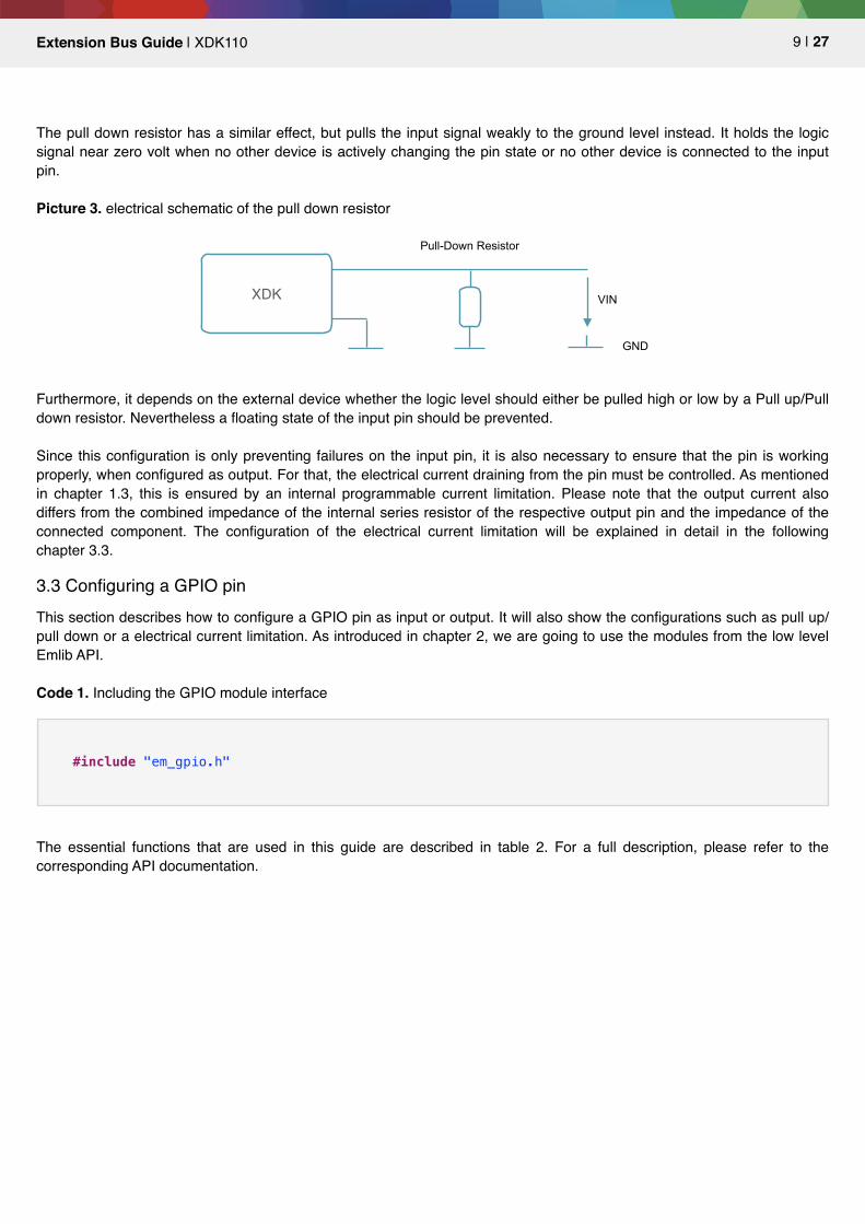
The pull down resistor has a similar effect, but pulls the input signal weakly to the ground level instead. It holds the logic signal near zero volt when no other device is actively changing the pin state or no other device is connected to the input pin.
Picture 3. electrical schematic of the pull down resistor
�
Furthermore, it depends on the external device whether the logic level should either be pulled high or low by a Pull up/Pull down resistor. Nevertheless a floating state of the input pin should be prevented.
Since this configuration is only preventing failures on the input pin, it is also necessary to ensure that the pin is working properly, when configured as output. For that, the electrical current draining from the pin must be controlled. As mentioned in chapter 1.3, this is ensured by an internal programmable current limitation. Please note that the output current also differs from the combined impedance of the internal series resistor of the respective output pin and the impedance of the connected component. The configuration of the electrical current limitation will be explained in detail in the following chapter 3.3.
3.3 Configuring a GPIO pinThis section describes how to configure a GPIO pin as input or output. It will also show the configurations such as pull up/pull down or a electrical current limitation. As introduced in chapter 2, we are going to use the modules from the low level Emlib API.
Code 1. Including the GPIO module interface
�
The essential functions that are used in this guide are described in table 2. For a full description, please refer to the corresponding API documentation.
XDK
GND
VIN
Pull-Down Resistor
#include "em_gpio.h"
� | �10 27Extension Bus Guide | XDK110
Table 2. GPIO interface (excerpt of em_gpio.h)
3.4 OutlineThe following code shows how a pin can be configured as input with a pull-up resistor.
Code 2. Configuring an input pin with pull-up resistor
�
The function GPIO_PinModeSet() is used to set the basic configuration. It sets the port location, called port register. It also sets the I/O mode configuration of the pin itself. This determines whether the pin is used as pull-up / pull-down, including an initial value.
The other function GPIO_PinOutSet() sets the output voltage level of the selected pin to high. If the pin is set to input mode, this will enable the pull-up resistor.
The configuration can also be done with a pull-down resistor. For that, only the second function call needs to be changed. GPIO_PinOutClear() has to be called after setting the Pin Mode, instead of GPIO_PinOutSet(), to pull the output voltage level to low, and as such, enable the pull-down resistor.
The overall effect of Code 2 is the configuration of pin PA1 as an input pin with a pull-up resistor.
To configure a pin as output, this can be done as simply as the configuration as input. The following outline shows this with the additional configuration of the electrical current limitation. Code 3. Configuring a GPIO pin as output
�
Before the selected pin's mode is set, the current drive mode is configured for the entire port. In the above code example the current drive mode for the complete port register A is set to the lowest current of 0.5 mA a single pin can provide.
FUNCTION DESCRIPTION
GPIO_PinModeSet This function is called to configure a specific pin in its Input/Output characteristic and to configure its mode (i.e pull-up/current limitation and so on).
GPIO_DriveModeSet This function is called to configure a specific port register in its current drive strength. This configures all pins of the respective register, when gpioModePushPullDrive is chosen as mode to configure a single pin.
GPIO_PinInGet This function is called to get the current voltage level on the chosen input pin.
GPIO_PinOutSet This function is called to set the current output voltage level to high.
GPIO_PinOutClear This function is called to set the current output voltage level to low.
Afterwards, the pin number one of the port register A is configured as gpioModePushPullDrive to make use of the previous configuration of the port register.
The following table shows which drive modes correspond to which current strength.
Table 3. Available configurable currents
Please note that without any current configuration, the default current drive mode of 6 mA is used. For more information, please refer to the data sheet of the EFM32GG390.
3.5 Writing and reading data from a GPIO pinThis section describes how to write data to an GPIO pin and how to read data from an GPIO pin, i.e. set and read the current logical state of the pin.
Writing to a GPIO pin is either to set the output, and as such write a logical "1" to the GPIO output or by clearing the output, and as such writing a logical "0" to the GPIO output.
The following code shows how to write a logical one to the GPIO output.
Code 4. Setting an output value to logical one
�
Code 5 shows how to write a logical zero to the same output.
Code 5. Setting an output value to logical zero
The input for both these functions is the port and the pin number of the respective pin. As such, the code snippets 4 and 5 respectively set and clear the output of pin PA1.
If a GPIO pin is configured as input, it can be read instead. Do note, the resulting value can only be a logical "1" or "0".
Please note that it is recommended to insert a pull-up or pull-down resistor to ensure that the input is not floating. Reading the pin's value, when no action from an external device (e.g. a button) is made, the logical read output will always have the logical value applied by the pull-up / pull-down resistor.
Additionally, depending on the pull-up / pull-down configuratiuon, the value produced by GPIO_PinInGet() is interpreted differently. For pull-up mode, the default value of the input is 1. That means, if the device attached to this pin is setting a logical 1, a logical 0 will be read on the pin. Therefore, a logical 0 returned by GPIO_PinInGet() represents the "ON"-state of the signal. On the other hand, if the mode is pull-down, the standard value will be a logical 0, which represents the "OFF"-state.
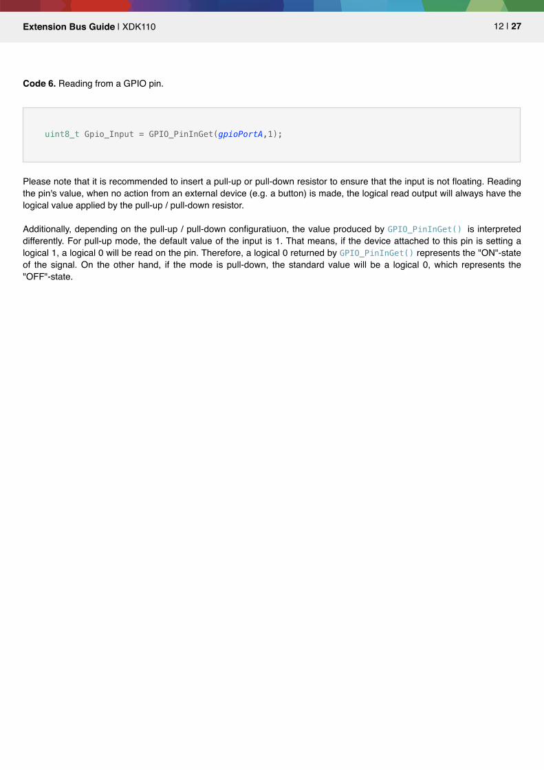
uint8_t Gpio_Input = GPIO_PinInGet(gpioPortA,1);
� | �13 27Extension Bus Guide | XDK110
4. Analog to Digital Converter (ADC)4.1 General IntroductionThe Analog to Digital Converter (ADC) is used to convert analog signals (such as a sound picked up by microphone) into a digital representation. Many applications need to measure analog signals and store them using a digital representation. Since microprocessors can only perform complex processing on digital values, the ADC provides a bridge between the analog world of signals, such as analog sensors and the digital world of signal- and data processing.
ADCs are used anywhere analog signals need to be processed, stored or transported in digital form.The MCU of the XDK uses a programmable 12 bit ADC with a reference voltage of up to 2.5 V. Two pins on the extension bus (PD5 and PD6) can be used as single ended inputs for the ADC. Single ended means, that these inputs can only measure analog voltages within a range from 0 to 2.5 V. Differential ended measurement of alternating input voltages cannot be used due to the use of the pins PD4 for the acoustic sensor and PD7 for battery monitoring.
4.2 Configuring the ADCThis section shows how to configure the ADC itself and the ADC pins PD5 and PD5 on the extension bus. As proposed in chapter 2, the ADC module of the low level Emlib API is used, especially since there is no higher level API available currently.
Code 7. Including the ADC module interface
�
The essential functions that are used in this guide are described in table 4. For a full description, please refer to the corresponding API documentation.
Table 4. ADC interface (excerpt of em_adc.h)
Additionally to the interface em_adc.h the following interfaces will be needed too.
#include "em_adc.h"
FUNCTION DESCRIPTION
ADC_Init() This function is called to initialize the ADC module of the MCU. This involves only configuring the ADC itself. The pin configuration is not covered by this function.
ADC_InitSingle() This function is called to initialize performing only a single conversion on one or multiple ADC input pins.
ADC_InitScan() This function is called to initialize performing a scan conversion on multiple ADC input pins.
ADC_Start() This function is used to start the ADC conversion on the configured ADC channel.
ADC_DataSingleGet() This function is used to read the data from the performed single conversion of one ADC channel.
ADC_DataScanGet() This function is used to read the data from multiple ADC channels performed by a scan conversion
� | �14 27Extension Bus Guide | XDK110
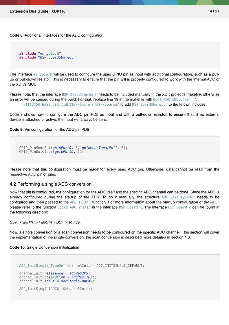
Code 8. Additional interfaces for the ADC configuration
�The interface em_gpio.h will be used to configure the used GPIO pin as input with additional configuration, such as a pull-up or pull-down resistor. This is necessary to ensure that the pin will is properly configured to work with the internal ADC of the XDK’s MCU.
Please note, that the interface BSP_BoardShared.h needs to be included manually in the XDK project’s makefile, otherwise an error will be caused during the build. For that, replace line 19 in the makefile with BCDS_XDK_INCLUDES = \ -I$(BCDS_BASE_DIR)/xdk110/Platform/BSP/source/ to add BSP_BoardShared.h to the known includes.
Code 9 shows how to configure the ADC pin PD5 as input and with a pull-down resistor, to ensure that, if no external device is attached or active, the input will always be zero.
Code 9. Pin configuration for the ADC pin PD5
�Please note that this configuration must be made for every used ADC pin. Otherwise, data cannot be read from the respective ADC pin or pins.
4.2 Performing a single ADC conversionNow that pin is configured, the configuration for the ADC itself and the specific ADC channel can be done. Since the ADC is already configured during the startup of the XDK. To do it manually, the structure ADC_Init_TypeDef needs to be configured and then passed to the ADC_Init() function. For more information about the startup configuration of the ADC, please refer to the function Board_ADC_init() in the interface BSP_Board.c. The interface BSP_Board.c can be found in the following directory:
SDK > xdk110 > Plaform > BSP > source
Now, a single conversion or a scan conversion needs to be configured on the specific ADC channel. This section will cover the implementation of the single conversion, the scan conversion is described more detailed in section 4.3.
The single conversion uses the structure ADC_InitSingle_TypeDef, where the ADC channel, the resolution on the channel and the reference voltage are configured.
Additional settings can also be made, but the ones used in Code 10 are the essential settings. Please refer to the complete definition of the structure ADC_InitSingle_TypeDef in em_adc.h for more options. In the code 10, the default values are configured by using the macro ADC_INITSINGLE_DEFAULT. Finally, the single conversion can be initialized by calling the function ADC_InitSingle().
After initializing the conversion, the conversion has to be started and the data can be read afterwards (after a brief delay). An example for reading the data is seen in Code 11.
Code 11. Reading of single converted ADC data
�First, the variable AdcSample is declared, where the read ADC value will be stored later. Afterwards, the function actively waits until no conversion is currently active. This is indicated by the bit ADC_STATUS_SINGLEACT. Then, the functions __enable_irq() and __disable_irq() are used to temporarily enable and disable interrupts used on the GPIO pins and the ADC is locked for a conversion. Afterwards, a single conversion is started. When the sampling conversion is finished, the value of ADC_STATUS_SINGLEACT is set to one. The function actively waits for this using a while-loop. Then, the received values first 12 bits are stored in AdcValue. Afterwards the interrupts for the GPIO pins are disabled, the ADC lock is opened and the GPIO pin interrupts are enabled again.
4.3 Performing a scan ADC conversionThis section explains how to configure the ADC to perform a scan conversion. The steps are quite similar to what has to be done for the single conversion.
Code 12. ADC Scan Conversion Initialization
�
uint32_t AdcSample = 0;
while ((ADC0->STATUS & (ADC_STATUS_SINGLEACT)) && (BSP_UNLOCKED == ADCLock));
// Wait while conversion is active while (ADC0->STATUS & (ADC_STATUS_SINGLEACT)); AdcSample = 0xFFF & ADC_DataSingleGet(ADC0); __disable_irq(); ADCLock = BSP_UNLOCKED; __enable_irq();
As before, a structure called ADC_InitScan_TypeDef is used to configure the scan conversion. The complete configuration can be set by using the default configuration defined in ADC_INITSCAN_DEFAULT.
In this example, only the reference voltage, the resolution and the input channels are configured specifically. Compared to the single conversion, this conversion has two inputs. These are set by using a bitwise OR operation with controller specific defines for channel 5 and 6 on the extension bus. Please note that a configuration, as implemented in Code 9, is still necessary for each of the used ADC pins. Afterwards the configuration is done and the scan conversion is initialized by passing the configuration into the function ADC_InitScan().
Reading is done similarly as it was done for the single conversion, except that two channels are started and read simultaneously, as shown in Code 13.
Code 13. Reading of scan converted ADC data
�Reading data from a scan conversion follows the same steps as reading the single conversion. For reading data, an array called AdcScanSample is declared at the beginning. In this array, the ADC data from the two ADC channels is stored. Similar as before, a verification is performed by reading the ADC_STATUS_SCANACT bit to check if a scan conversion is currently running. If this is not the case, the scan conversion can be started. Afterwards the data from the different ADC channels is stored into the AdcScanSample array in the same manner as in Code 11. The only difference here is that two channels have to be read one after another. Please note that for the scan conversion it is necessary to wait until until the bit ADC_STATUS_SCANDV is set. The bit itself signals that the register contains valid data as the result from the conversion of an ADC channel.
uint32_t AdcScanSample[] = {0,0};
while ((ADC0->STATUS & (ADC_STATUS_SCANACT)) && (BSP_UNLOCKED == ADCLock));
5. InterruptsFor the following two sections about timers and pulse counters, interrupts will play a major role in their implementation. As such, this section offers a short introduction to interrupts.
An interrupt is a commonly used technique in micro controllers, allowing CPU-external systems to indicate that a certain event happened, which may influence CPU execution. Interrupts do not require any action from the CPU unless they are triggered. This spares valuable processing time, since this removes the necessity of actively waiting for a certain event (such as "data ready") to appear.When an interrupt is triggered, the CPU will store its current state before the service routine and performs a task to handle certain events (e.g timer overflow, ADC conversion finish). After the task is finished, the CPU returns to where it left off before the interrupt was received.Since more than one interrupt can be triggered at the same time, different interrupt priorities can be assigned to Interrupt Requests (IRQ). This prevents important interrupt routines from idling too long, which can be critical in a real time context.
Please note that interrupts can also be applied to the ADC and the GPIO module as well.
� | �18 27Extension Bus Guide | XDK110
6. Clock ManagementClock management is also required, in addition to interrupts, for the following two sections about timers and pulse counters.
The Clock Management Unit (CMU) on a micro controller controls the oscillators and clocks. It can enable or disable the clock for the different peripherals separately, as well as enable, disable, or configure the available oscillators. This allows for minimizing energy consumption by disabling the clock for unused peripherals or having them run at lower frequencies.It is necessary for every utilized peripheral, such as the GPIO module, the ADC module or the timer and pulse counter module, that a specific clock is enabled for them.
In the case of the GPIO and ADC module, this is already done during the startup of the XDK via the execution of the systemStartup() function. This function calls BSP_Board_Initialize(), which covers the initialization of certain peripherals of the XDK, such as the GPIO and the ADC module.
Please note that the system startup functions can differ between version of the XDK-Workbench and it is recommended to enable the specific clock in the XDK application itself.
For the usage of the clock functionality, the interface em_cmu.h is used, which will be described in the following sections in more detail. For more information about the interface, please refer to the reference manual of the EFM32GG390.
7. Timer and Counter7.1 General IntroductionThe Timer and Counter modules keep track of timing and count events. It can generate output waveforms and trigger timed actions in other peripherals. Timers are beneficial when activities need to be timed precisely with as little CPU usage as possible.
The XDK's MCU features the following timer peripherals, which are used for specific tasks:
• Four 16 Bit Timer/Counter module• One 24 Bit and one 32 Bit Real-Time Counter• Three 8/16 Bit Pulse Counter• One Watchdog Timer
As can be seen, timers are also used in the watchdog and the real time counter module, as well as in the pulse counter module which will be explained in detail in section 8.
A timer can primarily be used for activities like up/down counting, input capture, output comparison and Pulse Width Modulation (PWM).
• Up-Count: The timer counts up until he reaches the configured maximal value. After that, the timer is reset to 0 before counting up again. As soon as the timer switches from the maximal value to 0, an interrupt can occur (as per configuration).
• Down-Count: The timer counts down from the maximal value to 0. After that, the timer is reloaded and restarts counting down from the maximal value. When the timer switches from 0 to the maximal value, an interrupt can occur (as per configuration).
• Up/Down-Count: The timer starts at 0 and counts up to the maximal configured value. Then it counts down to 0 and starts counting up again. Every time the value switches from the maximal value to the maximal value - 1, an overflow occurs. An underflow occurs, when the value goes from 0 to 1. Both events can trigger an interrupt.
• Input capture: This mode will capture the value of the counter based on a trigger event on the input pin.This can be used to measure pulse width or period.
• Output compare: This mode is used to compare an output value with the counter value. It is also possible to trigger a configured interrupt on a compare match.
• PWM: The timer has a separate mode for PWM generation, and it's only supported by up-count and down-count events.
� | �20 27Extension Bus Guide | XDK110
7.2 Configuring the TimerThis section shows how to configure the timer module to be used as counter. As proposed in section 2, the EMLib API for the timer module will be used, since it offers a lot of functionality which is currently not covered on higher API levels.
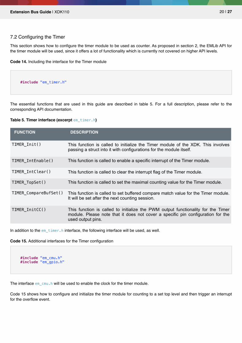
Code 14. Including the interface for the Timer module
�
The essential functions that are used in this guide are described in table 5. For a full description, please refer to the corresponding API documentation.
Table 5. Timer interface (excerpt em_timer.h)
In addition to the em_timer.h interface, the following interface will be used, as well.
Code 15. Additional interfaces for the Timer configuration
�
The interface em_cmu.h will be used to enable the clock for the timer module.
Code 15 shows how to configure and initialize the timer module for counting to a set top level and then trigger an interrupt for the overflow event.
#include "em_timer.h"
FUNCTION DESCRIPTION
TIMER_Init() This function is called to initialize the Timer module of the XDK. This involves passing a struct into it with configurations for the module itself.
TIMER_IntEnable() This function is called to enable a specific interrupt of the Timer module.
TIMER_IntClear() This function is called to clear the interrupt flag of the Timer module.
TIMER_TopSet() This function is called to set the maximal counting value for the Timer module.
TIMER_CompareBufSet() This function is called to set buffered compare match value for the Timer module. It will be set after the next counting session.
TIMER_InitCC() This function is called to initialize the PWM output functionality for the Timer module. Please note that it does not cover a specific pin configuration for the used output pins.
#include "em_cmu.h" #include "em_gpio.h"
� | �21 27Extension Bus Guide | XDK110
Code 16. Timer configuration
�The first function call of Code 16, CMU_ClockEnable() enables the clock for the timer module. Afterwards, a struct of the type TIMER_Init_TypeDef is declared and filled with default configuration parameters provided by the define TIMER_INIT_DEFAULT. Only specific configurations are made for the pre scaler and the timer mode. In this case the pre scaler is set up to 1024, that divides the used clock of 48 MHz down to approximately 48 kHz. The mode timerModeUp configures the timer for up counting up. Furthermore, the overflow interrupt of the timer module is enabled by calling the function Timer_IntEnable() and passing the parameter TIMER_IF_OF to it. Additionally, the timer interrupt is also enabled in the device specific interrupt controller of the XDK's MCU by calling the function NVIC_EnableIRQ().
Afterwards the maximal value is set by the function TIMER_TopSet() to ten, that the timer counts from 0 to 10 upwards and then triggers an overflow interrupt. Please note that the maximal value is not limited and can be set to any value to count up to.
Now that all configurations are made, the timer module can be initialized by calling the function TIMER_Init(). Please note that the timer directly starts counting after the initialization, because the enable parameter was already set by the default settings when making usage of TIMER_INIT_DEFAULT.
The last step is to define an interrupt handler for this particular timer. If none is defined, the application will not process the interrupt correctly.
The implementation of it is shown in Code 17 and needs to implemented before attempting to start the timer.
Code 17. Timer interrupt handler
�The signature for the interrupt handler should always be the same as it is shown in Code 17. The function call of TIMER_IntClear() inside the function is used to clear the interrupt overflow flag. If the flag is not cleared, no new counting up is started. Please note that it is essential to clear this flag within the interrupt handler. Additional functionality can be added before or after the call of TIMER_IntClear().
// Enable clock for TIMER0 module CMU_ClockEnable(cmuClock_TIMER0, true);
void TIMER0_IRQHandler(void){ TIMER_IntClear(TIMER0, TIMER_IF_OF); // Do something
portYIELD_FROM_ISR(pdTRUE);
}
� | �22 27Extension Bus Guide | XDK110
In most use cases, it is recommended to clear the flag first before executing any other functionality. Additionally, please note that the functionality should be kept short and simple, since an interrupt event occurs periodically in very short time intervals. As such, long processing chains should be avoided. Additionally, it is necessary to call the macro portYIELD_FROM_ISR() at the end of the interrupt handler too. This macro informs FreeRTOS that the interrupt is finished, so that execution can return to the context of the task that was interrupted.
This is necessary, because the interrupt from the timer module is a hardware interrupt with the highest priority and automatically interrupts the currently running operating task. To avoid issues with FreeRTOS, it is mandatory to return to the the initial task after the interrupt was processed.
Afterwards, no further implementation or configuration needs to be done.
7.3 Configuring the Timer for PWM usageThis chapter introduces how to use the PWM functionality of the timer module. This means that the output state of a pin, which can be controlled via the timer module, is changed during the interrupt events.
To do this, additional configuration needs to be applied to the pin and to the specific timer channel which controls that particular pin.
Code 18 shows which additional configuration need to be made.
Code 18. PWM pin configuration
�
As done in the previous sections, the pin needs to be configured via the em_gpio.h interface first, to act as an output with additional configuration such as push pull output. Afterwards, the timer channel itself needs to be configured. In this example, the GPIO pin PA0 on the extension bus is used. To ensure that this pin is used, the route parameter is set to location four, which indicates that PA0, PC0 and PC1 can be used to drive three phased actuators via the extension bus. Furthermore, the parameter TIMER_ROUTE_CC0PEN, enables that PA0 is used by the timer module.
For the timer channel itself multiple configurations can be made. For this the parameters of the configuration struct TIMER_InitCC_TypeDef are used. The essential configuration parameter are eventCtrl, edge, cmoa and mode.
The parameter event control eventCtrl is used to configure when a change to the output pin should be applied. Here, it is configured to apply on every event edge. That means that the state is changed on every triggered timer interrupt. Thus, the parameter edge configures if the state change is applied to the rising or falling edge of the triggered interrupt signal. The parameter cmoa stands for counter match output action and is configured to toggle the output pin. The parameter mode allows to configure the used mode. It can be configured for PWM, compare or capture. Here, it is configured for PWM.
Additionally, the same settings need to be made as in the previous chapter for the timer module itself.
Code 19 gives a short overview of this settings.
Code 19. Timer PWM configuration
All other parameter are not essential for the configuration and can either set to false or as be the parameters cufoa and cofoa which are used for compare and capture to timerOutActionNone. Please note that for the configuration the define TIMER_INITCC_DEFAULT can be used in the same manor as the TIMER_INIT_DEFAULT define and only the specific configuration need to be applied. Then the configuration struct TIMER_InitCC_TypeDef is passed to the function TIMER_InitCC() to initialize
Afterwards, the route location of the timer need to be set to location 4 to use the GPIO pin PA0 for PWM. This is necessary, because all GPIO pins on the extension bus can be used by multiple different modules. As such, one GPIO pin can be applied to six different modules.
�
The configuration of the timer module is similar as in Code 16. The necessary configuration for PWM usage is to configure up or down counting in the TIMER_Init_TypeDef struct. The function TIMER_TopSet() is used to configure the period for PWM the function and TIMER_CompareBufSet() is used for the relative turn on time. The first parameter of the function TIMER_CompareBufSet() indicates the timer module itself. The second parameter sets the timer channel and the last parameter the compare value, here 24000. This defines a duty cycle of 50 percent. Additionally, the function buffers the configured duty cycle and executes it after the next interrupt event occurs.
Please note that an interrupt handler as shown in code 17 is still needed. In that function, changes to the relative turn on time can be applied with the function TIMER_CompareBufSet(), as well. Additionally, please note that the timer module is also able to use two additional GPIO pins to drive 3 phase output actuators. For that, two additional channels on the route location 4 would need to be configured as shown in code 18.
// Please add this code into appInitSystem() under BCDS_UNUSED(param2); CMU_ClockEnable(cmuClock_TIMER0, true);
A Pulse Counter can be used for counting incoming pulses on a single input or to decode quadrature encoded inputs. It is mainly used to keep track of incoming pulses or rotations. It is used to capture the input signal from resolvers or any other types of rotatory encoders for position tracking. Single input counting allows only counting incoming pulses, whereas additionally counting on a second input allows to keep track of the rotating direction.
8.2 Configuring the Pulse Counter This section shows how to configure the pulse counter module to be used for overflow pulse counting. As proposed in chapter 2, the EMLib API for the pulse counter module will be used, since it offers a lot of functionality which is not covered on higher API levels.
Code 20. Including the interface for the pulse counter module
�
The essential functions that are used in this guide are described in table 6. For a full description, please refer to the corresponding API documentation.
Additionally to the em_pcnt.h interface, the following interface will be needed too.
Code 21. Additional interfaces for the pulse counter configuration
�
#include "em_pcnt.h"
FUNCTION DESCRIPTION
PCNT_Init() This function is called to initialize the Pulse Counter module of the XDK. This involves passing a struct into it with configurations for the module itself.
PCNT_IntEnable() This function is called to enable a chosen interrupt of the Pulse Counter module.
PCNT_IntClear() This function is called to clear the interrupt flag of the Timer module.
#include "em_cmu.h" #include "em_gpio.h"
� | �25 27Extension Bus Guide | XDK110
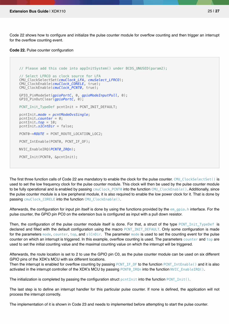
Code 22 shows how to configure and initialize the pulse counter module for overflow counting and then trigger an interrupt for the overflow counting event.
Code 22. Pulse counter configuration
�
The first three function calls of Code 22 are mandatory to enable the clock for the pulse counter. CMU_ClockSelectSet() is used to set the low frequency clock for the pulse counter module. This clock will then be used by the pulse counter module to be fully operational and is enabled by passing cmuClock_PCNT0 into the function CMU_ClockEnable(). Additionally, since the pulse counter module is a low peripheral module, it is also required to enable the low power clock for it. That is done by passing cmuClock_CORELE into the function CMU_ClockEnable().
Afterwards, the configuration for input pin itself is done by using the functions provided by the em_gpio.h interface. For the pulse counter, the GPIO pin PC0 on the extension bus is configured as input with a pull down resistor.
Then, the configuration of the pulse counter module itself is done. For that, a struct of the type PCNT_Init_TypeDef is declared and filled with the default configuration using the macro PCNT_INIT_DEFAULT. Only some configuration is made for the parameters mode, counter, top, and slCnDir. The parameter mode is used to set the counting event for the pulse counter on which an interrupt is triggered. In this example, overflow counting is used. The parameters counter and top are used to set the initial counting value and the maximal counting value on which the interrupt will be triggered.
Afterwards, the route location is set to 2 to use the GPIO pin C0, as the pulse counter module can be used on six different GPIO pins of the XDK's MCU with six different locations.Then the interrupt is enabled for overflow counting by passing PCNT_IF_OF to the function PCNT_IntEnable() and it is also activated in the interrupt controller of the XDK's MCU by passing PCNT0_IRQn into the function NVIC_EnableIRQ().
The initialization is completed by passing the configuration struct pcntInit into the function PCNT_Init().
The last step is to define an interrupt handler for this particular pulse counter. If none is defined, the application will not process the interrupt correctly.
The implementation of it is shown in Code 23 and needs to implemented before attempting to start the pulse counter.
// Please add this code into appInitSystem() under BCDS_UNUSED(param2);
// Select LFRCO as clock source for LFA CMU_ClockSelectSet(cmuClock_LFA, cmuSelect_LFRCO); CMU_ClockEnable(cmuClock_CORELE, true); CMU_ClockEnable(cmuClock_PCNT0, true);
�The signature for the interrupt handler should always be the same as it is shown in Code 23. The function call of TPCNT_IntClear() inside the function is used to clear the interrupt overflow flag. If the flag is not cleared, no new counting up is started. Please note that it is essential to clear this flag within the interrupt handler. Additional functionality can be added before or after the call of PCNT_IntClear().
In most use cases, it is recommended to clear the flag first before executing any other functionality. Additionally, please note that the functionality should be kept short and simple, since an interrupt event occurs periodically in very short time intervals. As such, long processing chains should be avoided. Additionally, it is necessary to call the macro portYIELD_FROM_ISR() at the end of the interrupt handler too. This macro informs FreeRTOS that the interrupt is finished, so that execution can return to the context of the task that was interrupted.
This is necessary, because the interrupt from the pulse counter module is a hardware interrupt with the highest priority and automatically interrupts the currently running operating task. To avoid issues with FreeRTOS, it is mandatory to return to the the initial task after the interrupt was processed.
Afterwards, no further implementation or configuration needs to be done.
void PCNT0_IRQHandler(void){ PCNT_IntClear(PCNT0, PCNT_IF_OF); // do something
portYIELD_FROM_ISR(pdTRUE); }
� | �27 27Extension Bus Guide | XDK110
9. Document History and Modification
REV. NO. CHAPTER DESCRIPTION OF MODIFICATION/CHANGES EDITOR DATE