44
LogiCORE IP Defective Pixel Correction v4.0 Product Guide PG005 October 19, 2011
LogiCORE IP Defective Pixel Correction v4.0Product Guide
PG005 October 19, 2011
LogiCORE IP Defective Pixel Correction www.xilinx.com 2PG005 October 19, 2011
Chapter 1: OverviewStandards Compliance . . . . . . . . . . . . . . . . . . . . . . . . . . . . . . . . . . . . . . . . . . . . . . . . . . . . . . . 5Feature Summary . . . . . . . . . . . . . . . . . . . . . . . . . . . . . . . . . . . . . . . . . . . . . . . . . . . . . . . . . . . . 5Licensing . . . . . . . . . . . . . . . . . . . . . . . . . . . . . . . . . . . . . . . . . . . . . . . . . . . . . . . . . . . . . . . . . . . . 6Installing Your License File . . . . . . . . . . . . . . . . . . . . . . . . . . . . . . . . . . . . . . . . . . . . . . . . . . 7Performance . . . . . . . . . . . . . . . . . . . . . . . . . . . . . . . . . . . . . . . . . . . . . . . . . . . . . . . . . . . . . . . . . 7Resource Utilization. . . . . . . . . . . . . . . . . . . . . . . . . . . . . . . . . . . . . . . . . . . . . . . . . . . . . . . . . . 7
Chapter 2: Core Interfaces and Register SpacePort Descriptions. . . . . . . . . . . . . . . . . . . . . . . . . . . . . . . . . . . . . . . . . . . . . . . . . . . . . . . . . . . . 10Register Space . . . . . . . . . . . . . . . . . . . . . . . . . . . . . . . . . . . . . . . . . . . . . . . . . . . . . . . . . . . . . . 14
Chapter 3: Customizing and Generating the CoreGraphical User Interface (GUI) . . . . . . . . . . . . . . . . . . . . . . . . . . . . . . . . . . . . . . . . . . . . . . 17Parameter Values in the XCO File . . . . . . . . . . . . . . . . . . . . . . . . . . . . . . . . . . . . . . . . . . . 18Output Generation . . . . . . . . . . . . . . . . . . . . . . . . . . . . . . . . . . . . . . . . . . . . . . . . . . . . . . . . . . 18
Chapter 4: Designing with the CoreGeneral Design Guidelines . . . . . . . . . . . . . . . . . . . . . . . . . . . . . . . . . . . . . . . . . . . . . . . . . 21Clocking . . . . . . . . . . . . . . . . . . . . . . . . . . . . . . . . . . . . . . . . . . . . . . . . . . . . . . . . . . . . . . . . . . . . 22Resets. . . . . . . . . . . . . . . . . . . . . . . . . . . . . . . . . . . . . . . . . . . . . . . . . . . . . . . . . . . . . . . . . . . . . . . 22Protocol Description . . . . . . . . . . . . . . . . . . . . . . . . . . . . . . . . . . . . . . . . . . . . . . . . . . . . . . . . 22
Chapter 5: Constraining the CoreRequired Constraints. . . . . . . . . . . . . . . . . . . . . . . . . . . . . . . . . . . . . . . . . . . . . . . . . . . . . . . . 23Device, Package, and Speed Grade Selections. . . . . . . . . . . . . . . . . . . . . . . . . . . . . . . . 23Clock Frequencies. . . . . . . . . . . . . . . . . . . . . . . . . . . . . . . . . . . . . . . . . . . . . . . . . . . . . . . . . . . 23Clock Management . . . . . . . . . . . . . . . . . . . . . . . . . . . . . . . . . . . . . . . . . . . . . . . . . . . . . . . . . 23Clock Placement . . . . . . . . . . . . . . . . . . . . . . . . . . . . . . . . . . . . . . . . . . . . . . . . . . . . . . . . . . . . 23Banking. . . . . . . . . . . . . . . . . . . . . . . . . . . . . . . . . . . . . . . . . . . . . . . . . . . . . . . . . . . . . . . . . . . . . 23Transceiver Placement . . . . . . . . . . . . . . . . . . . . . . . . . . . . . . . . . . . . . . . . . . . . . . . . . . . . . . 23I/O Standard and Placement . . . . . . . . . . . . . . . . . . . . . . . . . . . . . . . . . . . . . . . . . . . . . . . . . 23
Chapter 6: Detailed Example DesignDirectory and File Contents . . . . . . . . . . . . . . . . . . . . . . . . . . . . . . . . . . . . . . . . . . . . . . . . . 24Demonstration Test Bench . . . . . . . . . . . . . . . . . . . . . . . . . . . . . . . . . . . . . . . . . . . . . . . . . . 24Simulation . . . . . . . . . . . . . . . . . . . . . . . . . . . . . . . . . . . . . . . . . . . . . . . . . . . . . . . . . . . . . . . . . . 25Messages and Warnings . . . . . . . . . . . . . . . . . . . . . . . . . . . . . . . . . . . . . . . . . . . . . . . . . . . . . 25
Table of Contents
LogiCORE IP Defective Pixel Correction www.xilinx.com 3PG005 October 19, 2011
Appendix A: Verification, Compliance, and InteroperabilitySimulation . . . . . . . . . . . . . . . . . . . . . . . . . . . . . . . . . . . . . . . . . . . . . . . . . . . . . . . . . . . . . . . . . . 26Hardware Testing . . . . . . . . . . . . . . . . . . . . . . . . . . . . . . . . . . . . . . . . . . . . . . . . . . . . . . . . . . . 26
Appendix B: MigratingParameter Changes in the XCO File. . . . . . . . . . . . . . . . . . . . . . . . . . . . . . . . . . . . . . . . . . 27Port Changes . . . . . . . . . . . . . . . . . . . . . . . . . . . . . . . . . . . . . . . . . . . . . . . . . . . . . . . . . . . . . . . . 27Functionality Changes . . . . . . . . . . . . . . . . . . . . . . . . . . . . . . . . . . . . . . . . . . . . . . . . . . . . . . 27Special Considerations when Migrating to AXI . . . . . . . . . . . . . . . . . . . . . . . . . . . . . . 27
Appendix C: Debugging
Appendix D: Application Software DevelopmentProgrammer's Guide . . . . . . . . . . . . . . . . . . . . . . . . . . . . . . . . . . . . . . . . . . . . . . . . . . . . . . . . 29
Appendix E: C Model ReferenceFeatures. . . . . . . . . . . . . . . . . . . . . . . . . . . . . . . . . . . . . . . . . . . . . . . . . . . . . . . . . . . . . . . . . . . . . 32 . . . . . . . . . . . . . . . . . . . . . . . . . . . . . . . . . . . . . . . . . . . . . . . . . . . . . . . . . . . . . Overview 32Additional Core Resources . . . . . . . . . . . . . . . . . . . . . . . . . . . . . . . . . . . . . . . . . . . . . . . . . . 32Technical Support. . . . . . . . . . . . . . . . . . . . . . . . . . . . . . . . . . . . . . . . . . . . . . . . . . . . . . . . . . . 33Feedback. . . . . . . . . . . . . . . . . . . . . . . . . . . . . . . . . . . . . . . . . . . . . . . . . . . . . . . . . . . . . . . . . . . . 33Software Requirements . . . . . . . . . . . . . . . . . . . . . . . . . . . . . . . . . . . . . . . . . . . . . . . . . . . . . 33Unpacking and Model Contents . . . . . . . . . . . . . . . . . . . . . . . . . . . . . . . . . . . . . . . . . . . . . 34Installation . . . . . . . . . . . . . . . . . . . . . . . . . . . . . . . . . . . . . . . . . . . . . . . . . . . . . . . . . . . . . . . . . 35Defective Pixel Correction v4.0 Bit Accurate C Model . . . . . . . . . . . . . . . . . . . . . . . . 35C Model Example Code . . . . . . . . . . . . . . . . . . . . . . . . . . . . . . . . . . . . . . . . . . . . . . . . . . . . . 40Compiling the Example with the Defective Pixel Correction C Model . . . . . . . . 41Running the Example, Evaluating Results . . . . . . . . . . . . . . . . . . . . . . . . . . . . . . . . . . . 41
Appendix F: Additional ResourcesXilinx Resources . . . . . . . . . . . . . . . . . . . . . . . . . . . . . . . . . . . . . . . . . . . . . . . . . . . . . . . . . . . . 43Solution Centers . . . . . . . . . . . . . . . . . . . . . . . . . . . . . . . . . . . . . . . . . . . . . . . . . . . . . . . . . . . . 43References . . . . . . . . . . . . . . . . . . . . . . . . . . . . . . . . . . . . . . . . . . . . . . . . . . . . . . . . . . . . . . . . . . 43Technical Support. . . . . . . . . . . . . . . . . . . . . . . . . . . . . . . . . . . . . . . . . . . . . . . . . . . . . . . . . . . 43Ordering Information . . . . . . . . . . . . . . . . . . . . . . . . . . . . . . . . . . . . . . . . . . . . . . . . . . . . . . . 44Revision History . . . . . . . . . . . . . . . . . . . . . . . . . . . . . . . . . . . . . . . . . . . . . . . . . . . . . . . . . . . . 44Notice of Disclaimer . . . . . . . . . . . . . . . . . . . . . . . . . . . . . . . . . . . . . . . . . . . . . . . . . . . . . . . . 44
LogiCORE IP Defective Pixel Correction www.xilinx.com 4PG003 October 19, 2011 Product Specification
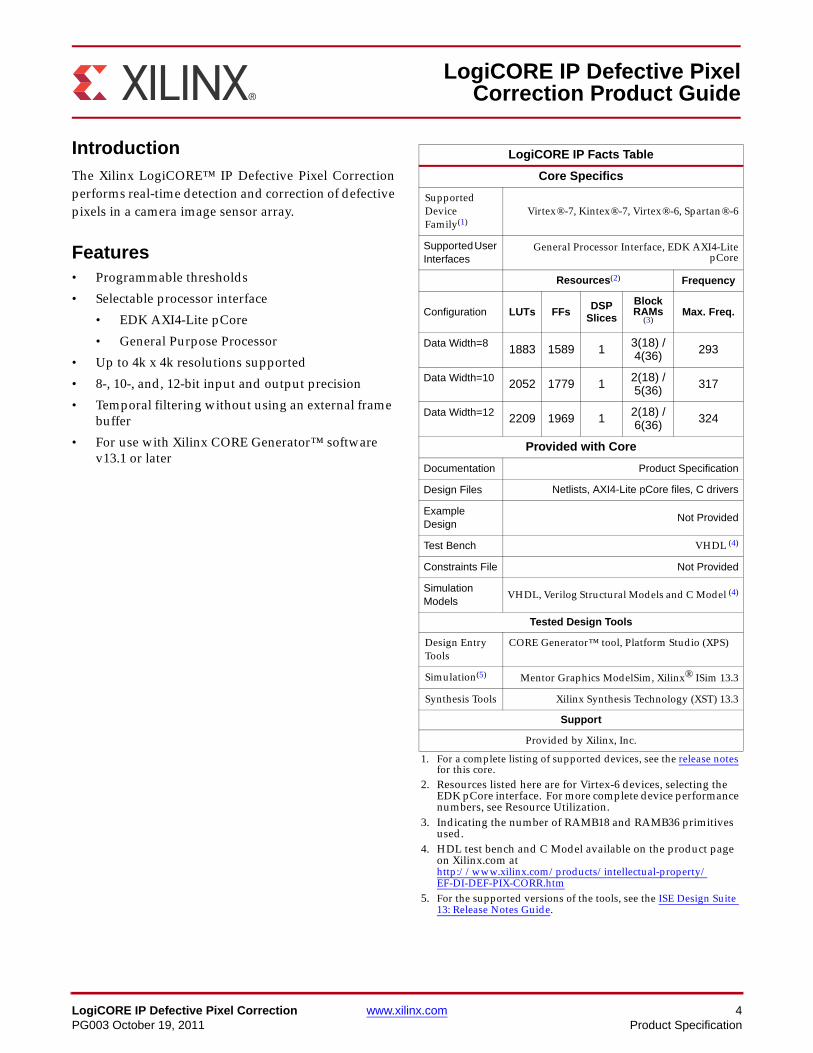
IntroductionThe Xilinx LogiCORE™ IP Defective Pixel Correctionperforms real-time detection and correction of defectivepixels in a camera image sensor array.
Features• Programmable thresholds
• Selectable processor interface
• EDK AXI4-Lite pCore
• General Purpose Processor
• Up to 4k x 4k resolutions supported
• 8-, 10-, and, 12-bit input and output precision
• Temporal filtering without using an external frame buffer
• For use with Xilinx CORE Generator™ software v13.1 or later
LogiCORE IP Defective PixelCorrection Product Guide
LogiCORE IP Facts Table
Core Specifics
Supported Device Family(1)
Virtex®-7, Kintex®-7, Virtex®-6, Spartan®-6
Supported User Interfaces
General Processor Interface, EDK AXI4-LitepCore
Resources(2) Frequency
Configuration LUTs FFs DSP Slices
Block RAMs
(3)Max. Freq.
Data Width=8 1883 1589 1 3(18) / 4(36) 293
Data Width=10 2052 1779 1 2(18) / 5(36) 317
Data Width=12 2209 1969 1 2(18) / 6(36) 324
Provided with Core
Documentation Product Specification
Design Files Netlists, AXI4-Lite pCore files, C drivers
Example Design
Not Provided
Test Bench VHDL (4)
Constraints File Not Provided
Simulation Models
VHDL, Verilog Structural Models and C Model (4)
Tested Design Tools
Design Entry Tools
CORE Generator™ tool, Platform Studio (XPS)
Simulation(5) Mentor Graphics ModelSim, Xilinx® ISim 13.3
Synthesis Tools Xilinx Synthesis Technology (XST) 13.3
Support
Provided by Xilinx, Inc.
1. For a complete listing of supported devices, see the release notes for this core.
2. Resources listed here are for Virtex-6 devices, selecting the EDK pCore interface. For more complete device performance numbers, see Resource Utilization.
3. Indicating the number of RAMB18 and RAMB36 primitives used.
4. HDL test bench and C Model available on the product page on Xilinx.com at http://www.xilinx.com/products/intellectual-property/EF-DI-DEF-PIX-CORR.htm
5. For the supported versions of the tools, see the ISE Design Suite 13: Release Notes Guide.
LogiCORE IP Defective Pixel Correction www.xilinx.com 5PG005 October 19, 2011 Product Specification
Chapter 1
Overview
An image sensor may have a certain number of defective pixels that may be the result of manufacturing faults, failures during normal operation, or variations in pixel voltage levels based on temperature or exposure. A wide class of pixel defects may be characterized as: dead (always low), hot (always high), or stuck (to a certain value). These anomalies can further be characterized as static (always present) or dynamic (as a function of exposure or temperature).
The Xilinx Defective Pixel Correction solution distinguishes between large stationary areas, which are likely to be non-changing parts of the image, and singular outliers, which are likely to be defective pixels. The Xilinx Defective Pixel Correction solution compares a pixel in the raw, Bayer sub-sampled domain to its neighboring, same color pixel values and keeps track of pixels that are sufficiently different from their neighbors. If the values of tracked outlier pixels stay in a predefined range for a predefined number of frames, then the tracked pixels are considered defective, and are replaced with values interpolated from neighboring pixels.
Spatial filtering first identifies potential defective pixels, and at the same time eliminates pixels that blend into their local neighborhoods, and therefore do not need to be substituted even if they are defective. Spatial filtering reduces the number of pixels, along with the amount of information, that needs to be stored for temporal filtering, therefore facilitating spatio-temporal filtering in embedded systems with limited or no access to external memory.
Standards ComplianceThe Defective Pixel Correction core is compliant with the AXI4-Lite interconnect standard as defined in the AXI Reference Guide (UG761).
Feature SummaryThe Defective Pixel Correction core performs real-time detection and correction of defective pixels in a camera image sensor array. The core is capable of removing defective pixels in real time, without the need to buffer, on a maximum resolution of 4096 columns by 4096 rows 8, 10, or 12 bits per pixel and supports the bandwidth necessary for High-definition (1080p60) resolutions.
You can generate the core as an EDK pCore (AXI4-Lite interconnect) or as a generic General Purpose Processor interface where all the user register connections are exposed as ports to the core. These two interfaces are described in Chapter 2, Core Interfaces and Register Space.
LogiCORE IP Defective Pixel Correction www.xilinx.com 6PG005 October 19, 2011 Product Specification
Chapter 1: Overview
LicensingThe Defective Pixel Correction core provides the following three licensing options:
• Simulation Only
• Full System Hardware Evaluation
• Full
After installing the required Xilinx ISE software and IP Service Packs, choose a license option.
Simulation Only The Simulation Only Evaluation license key is provided with the Xilinx CORE Generator tool. This key lets you assess core functionality with either the example design provided with the Defective Pixel Correction core, or alongside your own design and demonstrates the various interfaces to the core in simulation. (Functional simulation is supported by a dynamically generated HDL structural model.)
No action is required to obtain the Simulation Only Evaluation license key; it is provided by default with the Xilinx CORE Generator software.
Full System Hardware Evaluation The Full System Hardware Evaluation license is available at no cost and lets you fully integrate the core into an FPGA design, place-and-route the design, evaluate timing, and perform functional simulation of the Defective Pixel Correction core using the example design and demonstration test bench provided with the core.
In addition, the license key lets you generate a bitstream from the placed and routed design, which can then be downloaded to a supported device and tested in hardware. The core can be tested in the target device for a limited time before timing out (resetting to default values and the output video becoming black), at which time it can be reactivated by reconfiguring the device.
The timeout period for this core is set to approximately 8 hours for a 74.25 MHz clock. Using a faster or slower clock will change the timeout period proportionally. For example, using a 150 MHz clock will result in a timeout period of approximately 4 hours.
To obtain a Full System Hardware Evaluation license, do the following:
1. Navigate to the product page for this core.
2. Click Evaluate. 3. Follow the instructions to install the required Xilinx ISE software and IP Service Packs.
FullThe Full license key is available when you purchase the core and provides full access to all core functionality both in simulation and in hardware, including:
• Functional simulation support • Full implementation support including place and route and bitstream generation • Full functionality in the programmed device with no time outs
To obtain a Full license key, you must purchase a license for the core. Click on the "Order" link on the Xilinx.com IP core product page for information on purchasing a license for this
LogiCORE IP Defective Pixel Correction www.xilinx.com 7PG005 October 19, 2011 Product Specification
Chapter 1: Overview
core. After doing so, click the "How do I generate a license key to activate this core?" link on the Xilinx.com IP core product page for further instructions.
Installing Your License FileThe Simulation Only Evaluation license key is provided with the ISE CORE Generator system and does not require installation of an additional license file. For the Full System Hardware Evaluation license and the Full license, an email will be sent to you containing instructions for installing your license file. Additional details about IP license key installation can be found in the ISE Design Suite Installation, Licensing and Release Notes document.
PerformanceThe following sections detail the performance characteristics of the Defective Pixel Correction core.
Maximum FrequenciesThe following are typical clock frequencies for the target devices. The maximum achievable clock frequency can vary. The maximum achievable clock frequency and all resource counts can be affected by other tool options, additional logic in the FPGA device, using a different version of Xilinx tools and other factors.
• Virtex®-7 FPGA: 264 MHz
• Kintex™-7 FPGA: 282 MHz
• Virtex-6 FPGA: 324 MHz
• Spartan®-6 FPGA: 196 MHz
ThroughputThe Defective Pixel Correction core produces as much data as it consumes. If timing constraints are met, the throughput is equal to the rate at which video data is written into the core. In numeric terms, 1080P/60 RGB represents an average data rate of 124.4 Mpixels/sec or a burst data rate of 148.5 Mpixels/sec.
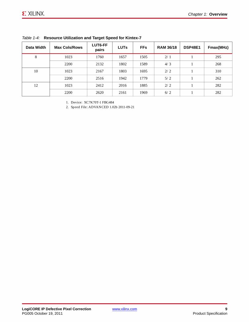
Resource UtilizationFor an accurate measure of the usage of device resources (for example, block RAMs, flip-flops, and LUTs) for a particular instance, click View Resource Utilization in CORE Generator after generating the core.
Information provided in Table 1-1 - Table 1-4 is a guideline to the resource utilization of the Defective Pixel Correction core for Spartan-6, Virtex-6, Virtex-7, and Kintex-7 FPGA families. This core does not use any XtremeDSP slices, block RAM, dedicated I/O, or clock resources. The design was tested using Xilinx ISE® v13.3 tools with default tool options, using timing constraints.

LogiCORE IP Defective Pixel Correction www.xilinx.com 8PG005 October 19, 2011 Product Specification
Chapter 1: Overview
1. Device: XC6SLX150-2 FGG9002. Speed File: PRODUCTION 1.20c 2011-09-21
1. Device: XC6VLX75T-1 FF4842. Speed File: PRODUCTION 1.15 2011-09-21
1. Device: XC7V585T-1 FFG11572. Speed File: ADVANCED 1.02i 2011-09-21
Table 1-1: Resource Utilization and Target Speed for Spartan-6
Data Width Max Cols/RowsLUT6-FF
pairsLUTs FFs RAMB 16/8 DSP48A1 Fmax(MHz)
8 1023 2063 1668 1601 4/1 1 196
2200 2223 1832 1693 11/0 1 196
10 1023 2222 1876 1801 5/1 1 196
2200 2362 2012 1893 13/0 1 203
12 1023 2439 2024 2001 6/0 1 210
2200 2722 2114 2093 15/0 1 189
Table 1-2: Resource Utilization and Target Speed for Virtex-6
Data Width Max Cols/RowsLUT6-FF
pairsLUTs FFs RAM 36/18 DSP48E1 Fmax(MHz)
8 1023 1984 1695 1505 2/1 1 324
2200 2206 1883 1589 4/3 1 293
10 1023 2144 1826 1695 2/2 1 349
2200 2310 2052 1779 5/2 1 317
12 1023 2483 2005 1885 2/2 1 305
2200 2557 2209 1969 6/2 1 324
Table 1-3: Resource Utilization and Target Speed for Virtex-7
Data Width Max Cols/RowsLUT6-FF
pairsLUTs FFs RAM 36/18 DSP48E1 Fmax(MHz)
8 1023 2042 1648 1505 2/1 1 291
2200 2214 1787 1589 4/3 1 264
10 1023 2208 1807 1695 2/2 1 264
2200 2451 1982 1779 5/2 1 239
12 1023 2398 1995 1885 2/2 1 309
2200 2539 2199 1969 6/2 1 291
LogiCORE IP Defective Pixel Correction www.xilinx.com 9PG005 October 19, 2011 Product Specification
Chapter 1: Overview
1. Device: XC7K70T-1 FBG4842. Speed File: ADVANCED 1.02b 2011-09-21
Table 1-4: Resource Utilization and Target Speed for Kintex-7
Data Width Max Cols/RowsLUT6-FF
pairsLUTs FFs RAM 36/18 DSP48E1 Fmax(MHz)
8 1023 1760 1657 1505 2/1 1 295
2200 2132 1802 1589 4/3 1 268
10 1023 2167 1803 1695 2/2 1 310
2200 2516 1942 1779 5/2 1 262
12 1023 2412 2016 1885 2/2 1 282
2200 2620 2161 1969 6/2 1 282

LogiCORE IP Defective Pixel Correction www.xilinx.com 10PG005 October 19, 2011
Chapter 2
Core Interfaces and Register Space
Port Descriptions
Processor InterfacesThe Defective Pixel Correction core supports the following two processor interface options:
• General Purpose Processor Interface
• EDK pCore Interface
The processor interfaces provide the system designer with the ability to dynamically control the parameters within the core.
General Purpose Processor Interface
The General Purpose Processor Interface exposes the thresholds and control signals as ports. The Core Symbol for the General Purpose Processor Interface is shown in Figure 2-1. These ports are described in Table 2-1. The ports common to all interfaces are described in Table 2-4.
X-Ref Target - Figure 2-1
Figure 2-1: Core Symbol for the General Purpose Processor Interface

LogiCORE IP Defective Pixel Correction www.xilinx.com 11PG005 October 19, 2011
Chapter 2: Core Interfaces and Register Space
The General Purpose Processor Interface exposes the thresholds and control registers as ports. This option is very useful for users designing a system with a user-defined bus interface (decoding logic and register banks) to an arbitrary processor.
The threshold ports have the double-buffer control mechanism described in the previous section to prevent tearing or committing partially updated port values. However, the first set of registers (shadow register bank) has to be supplied by the user-defined bus interface. Values from this register bank (external to the Defective Pixel Correction core) are copied over to the internal registers at the rising edge of vblank_in when bit 1 of the control is set to 1.
See also the General Purpose Processor Interface section of Port Descriptions.
EDK pCore Interface
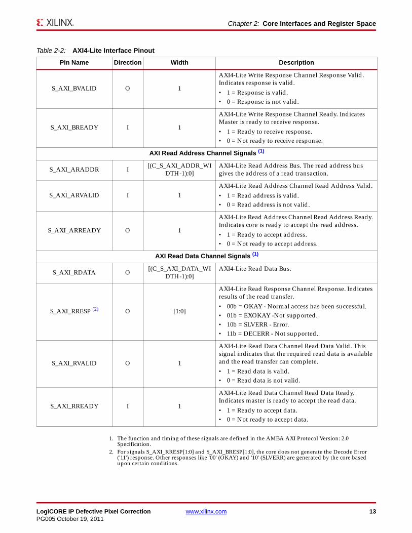
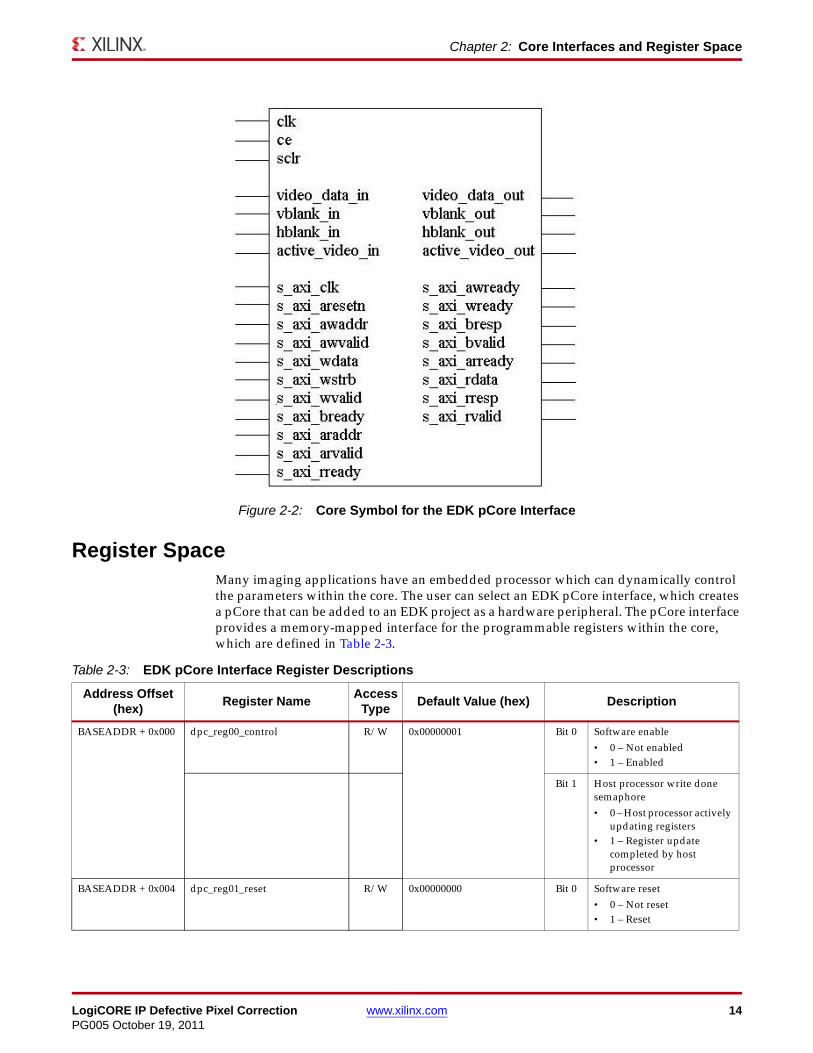
The EDK pCore Interface generates AXI4-Lite interface ports in addition to the common ports described in Table 2-4. The AXI4-Lite signals are automatically connected when the generated pCore is inserted into an EDK project. The AXI4-Lite signals are listed in Table 2-3. For more information on the AXI4-Lite signals, see AXI Reference Guide. The Core Symbol for the EDK pCore Interface is shown in Figure 2-2..
Table 2-1: Additional Ports for the General Purpose Processor Interface
Port Name Port Width Direction Description
control 2 IN • Bit 0: Software enable• Bit 1: Host processor write done semaphore
• 0 indicates host processor actively updating registers
• 1 indicates register update completed by host processor
thresh_temporal_var
DATA_WIDTH IN Allowed inter-frame variance of defective pixels
thresh_spatial_var 16 IN Allowed spatial variance beyond which a pixel is characterized as an outlier
thresh_pixel_age 16 IN Number of frames an outlier pixel has to keep its value within the range specified
status 8 OUT Status register
• Bit 0: FIFO empty• Bit 1: FIFO full• Bit 2-6: Reserved• Bit 7: Timing lock output; '1' indicates that the
timing module of the core has locked on the input timing signals and is generating stable output timing signals
num_candidates STATUS_WIDTH OUT Total number of potential defective pixel candidates stored in FIFO (in previous frame)
num_defective STATUS_WIDTH OUT Total number of pixels being actively interpolated (in previous frame)

LogiCORE IP Defective Pixel Correction www.xilinx.com 12PG005 October 19, 2011
Chapter 2: Core Interfaces and Register Space
Table 2-2: AXI4-Lite Interface Pinout
Pin Name Direction Width Description
AXI Global System Signals (1)
S_AXI_ACLK I 1 AXI Clock
S_AXI_ARESETN I 1 AXI Reset, active Low
IP2INTC_Irpt O 1 Interrupt request output
AXI Write Address Channel Signals (1)
S_AXI_AWADDR I [(C_S_AXI_ADDR_WI
DTH-1):0] AXI4-Lite Write Address Bus. The write address bus gives the address of the write transaction.
S_AXI_AWVALID I 1
AXI4-Lite Write Address Channel Write Address Valid. This signal indicates that valid write address is available.
• 1 = Write address is valid. • 0 = Write address is not valid.
S_AXI_AWREADY O 1
AXI4-Lite Write Address Channel Write Address Ready. Indicates core is ready to accept the write address.
• 1 = Ready to accept address.• 0 = Not ready to accept address.
AXI Write Data Channel Signals (1)
S_AXI_WDATA I [(C_S_AXI_DATA_WIDTH-1):0]
AXI4-Lite Write Data Bus.
S_AXI_WSTRB I [C_S_AXI_DATA_WIDTH/8-1:0]
AXI4-Lite Write Strobes. This signal indicates which byte lanes to update in memory.
S_AXI_WVALID I 1
AXI4-Lite Write Data Channel Write Data Valid. This signal indicates that valid write data and strobes are available.
• 1 = Write data/strobes are valid. • 0 = Write data/strobes are not valid.
S_AXI_WREADY O 1
AXI4-Lite Write Data Channel Write Data Ready. Indicates core is ready to accept the write data.
• 1 = Ready to accept data.• 0 = Not ready to accept data.
AXI Write Response Channel Signals (1)
S_AXI_BRESP (2) O [1:0]
AXI4-Lite Write Response Channel. Indicates results of the write transfer.
• 00b = OKAY - Normal access has been successful. • 01b = EXOKAY -Not supported. • 10b = SLVERR - Error. • 11b = DECERR - Not supported.
LogiCORE IP Defective Pixel Correction www.xilinx.com 13PG005 October 19, 2011
Chapter 2: Core Interfaces and Register Space
1. The function and timing of these signals are defined in the AMBA AXI Protocol Version: 2.0 Specification.
2. For signals S_AXI_RRESP[1:0] and S_AXI_BRESP[1:0], the core does not generate the Decode Error ('11') response. Other responses like '00' (OKAY) and '10' (SLVERR) are generated by the core based upon certain conditions.
S_AXI_BVALID O 1
AXI4-Lite Write Response Channel Response Valid. Indicates response is valid.
• 1 = Response is valid.• 0 = Response is not valid.
S_AXI_BREADY I 1
AXI4-Lite Write Response Channel Ready. Indicates Master is ready to receive response.
• 1 = Ready to receive response.• 0 = Not ready to receive response.
AXI Read Address Channel Signals (1)
S_AXI_ARADDR I [(C_S_AXI_ADDR_WI
DTH-1):0] AXI4-Lite Read Address Bus. The read address bus gives the address of a read transaction.
S_AXI_ARVALID I 1 AXI4-Lite Read Address Channel Read Address Valid.
• 1 = Read address is valid. • 0 = Read address is not valid.
S_AXI_ARREADY O 1
AXI4-Lite Read Address Channel Read Address Ready. Indicates core is ready to accept the read address.
• 1 = Ready to accept address. • 0 = Not ready to accept address.
AXI Read Data Channel Signals (1)
S_AXI_RDATA O [(C_S_AXI_DATA_WIDTH-1):0]
AXI4-Lite Read Data Bus.
S_AXI_RRESP (2) O [1:0]
AXI4-Lite Read Response Channel Response. Indicates results of the read transfer.
• 00b = OKAY - Normal access has been successful. • 01b = EXOKAY -Not supported. • 10b = SLVERR - Error.• 11b = DECERR - Not supported.
S_AXI_RVALID O 1
AXI4-Lite Read Data Channel Read Data Valid. This signal indicates that the required read data is available and the read transfer can complete.
• 1 = Read data is valid. • 0 = Read data is not valid.
S_AXI_RREADY I 1
AXI4-Lite Read Data Channel Read Data Ready. Indicates master is ready to accept the read data.
• 1 = Ready to accept data.• 0 = Not ready to accept data.
Table 2-2: AXI4-Lite Interface Pinout
Pin Name Direction Width Description
LogiCORE IP Defective Pixel Correction www.xilinx.com 14PG005 October 19, 2011
Chapter 2: Core Interfaces and Register Space
Register SpaceMany imaging applications have an embedded processor which can dynamically control the parameters within the core. The user can select an EDK pCore interface, which creates a pCore that can be added to an EDK project as a hardware peripheral. The pCore interface provides a memory-mapped interface for the programmable registers within the core, which are defined in Table 2-3.
X-Ref Target - Figure 2-2
Figure 2-2: Core Symbol for the EDK pCore Interface
Table 2-3: EDK pCore Interface Register Descriptions
Address Offset (hex)
Register NameAccess
TypeDefault Value (hex) Description
BASEADDR + 0x000 dpc_reg00_control R/W 0x00000001 Bit 0 Software enable• 0 – Not enabled• 1 – Enabled
Bit 1 Host processor write done semaphore• 0 – Host processor actively
updating registers• 1 – Register update
completed by host processor
BASEADDR + 0x004 dpc_reg01_reset R/W 0x00000000 Bit 0 Software reset• 0 – Not reset• 1 – Reset

LogiCORE IP Defective Pixel Correction www.xilinx.com 15PG005 October 19, 2011
Chapter 2: Core Interfaces and Register Space
All of the registers are readable, enabling you to verify writes or read back current values.
The core has a feature that allows it to be enabled or disabled. This halts the operation of the core by blocking the propagation of all video signals. This function is controlled by setting the Software Enable, bit 0 of dpc_reg00_control register, to 0; the default value of Software Enable is 1 (enabled).
The core can be effectively reset in-system by asserting dpc_reg01_reset (bit 0), which resets the timing and returns the thresholds to their default values. The core control signals and output are forced to 0 until the software reset bit is deasserted.
All registers other than the dpc_reg00_control, dpc_reg01_reset, and dpc_reg02_status registers are double-buffered in hardware, to ensure no image tearing happens if the threshold values are modified in the active area of a frame. This double-buffering provides a more flexible and easier-to-use core because it decouples the register updates from the blanking period, allowing software a much larger window with which to update the parameter values. The updated values for the threshold registers are latched into the shadow registers immediately after writing them, while the actual thresholds used are stored in the working registers.
Any reads of registers during operation will return the values stored in the shadow registers. The rising edge of vblank_in triggers the values from the shadow registers to be copied to the working registers, when bit 1 of dpc_reg00_control is set to 1. This semaphore bit helps to prevent partially updated shadow registers from being copied over to the working registers.
See the clk - clock: Master clock in the design, synchronous with, or identical to the video clock. section of Port Descriptions.
BASEADDR + 0x008 dpc_reg02_status R 0x00000001 Bit 0 FIFO Empty
Bit 1 FIFO Full
Bit 2-6 Reserved
Bit 7 Timing lock output'1' indicates that the timing module of the core has locked on the input timing signals and is generating stable output timing signals
BASEADDR + 0x00C dpc_reg03_thresh_temporal_var R/W 2**(DATA_WIDTH-7) Allowed inter-frame variance of defective pixels
BASEADDR + 0x010 dpc_reg04_thresh_spatial_var R/W 0x0000199A Allowed spatial variance beyond which a pixel is characterized as an outlier
BASEADDR + 0x014 dpc_reg05_thresh_pixel_age R/W 0x000004B0 Number of frames an outlier pixel has to keep its value within the range specified
BASEADDR + 0x018 dpc_reg06_num_candidates R 0x00000000 Total number of potential defective pixel candidates stored in FIFO (in previous frame)
BASEADDR + 0x01C
dpc_reg07_num_defective R 0x00000000 Total number of pixels being actively interpolated (in previous frame)
Table 2-3: EDK pCore Interface Register Descriptions (Cont’d)
LogiCORE IP Defective Pixel Correction www.xilinx.com 16PG005 October 19, 2011
Chapter 2: Core Interfaces and Register Space
Common I/O SignalsThe EDK pCore interface and the General Purpose Processor interface share a number of the same Input/Output (I/O) signals. The following set of signals is common to both interface options and to all video iPipe cores. Table 2-4 contains general port information, followed by a more detailed description of each port.
• clk - clock: Master clock in the design, synchronous with, or identical to the video clock.
• ce - clock enable: Pulling CE low suspends all operations within the core. Outputs are held, and no input signals are sampled, except for reset (SCLR takes precedence over CE).
• sclr - synchronous clear: Pulling SCLR high results in resetting all output pins to zero or their default values.
• video_data_in: This bus contains the video input in DATA_WIDTH bits wide unsigned integer representation. The input is assumed to be from a Bayer sub-sampled image.
• hblank_in. The hblank_in signal conveys information about the blank/non-blank regions of video scan lines.
• vblank_in: The vblank_in signal conveys information about the blank/non-blank regions of video frames, and is used by the Defective Pixel Correction core to detect end of a frame, when user registers can be copied to active registers to avoid visual tearing of the image.
• active_video_in: The active_video_in signal is high when valid data is presented at the input.
• video_data_out: This bus contains video output represented as DATA_WIDTH bits wide unsigned integers. The output is in the format of Bayer sub-sampled data.
• hblank_out, vblank_out, and active_video_out: The corresponding input signals are delayed so blanking outputs are in phase with the video data output, maintaining the integrity of the video stream.
Table 2-4: Port Descriptions
Port Name Port Width Direction Description
clk 1 IN Rising-edge clock
ce 1 IN Clock enable (active high)
sclr 1 IN Synchronous clear – reset (active high)
video_data_in DATA_WIDTH IN Data input bus
hblank_in 1 IN Horizontal blanking input
vblank_in 1 IN Vertical blanking input
active_video_in 1 IN Active video signal input
video_data_out DATA_WIDTH OUT Data output bus
hblank_out 1 OUT Horizontal blanking output
vblank_out 1 OUT Vertical blanking output
active_video_out 1 OUT Active video signal output
LogiCORE IP Defective Pixel Correction www.xilinx.com 17PG005 October 19, 2011
Chapter 3
Customizing and Generating the Core
This chapter includes information on using Xilinx tools to customize and generate the core.
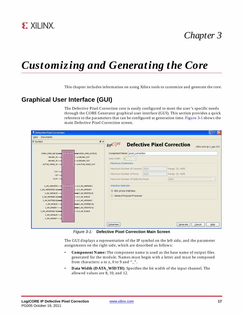
Graphical User Interface (GUI)The Defective Pixel Correction core is easily configured to meet the user’s specific needs through the CORE Generator graphical user interface (GUI). This section provides a quick reference to the parameters that can be configured at generation time. Figure 3-1 shows the main Defective Pixel Correction screen.
The GUI displays a representation of the IP symbol on the left side, and the parameter assignments on the right side, which are described as follows:
• Component Name: The component name is used as the base name of output files generated for the module. Names must begin with a letter and must be composed from characters: a to z, 0 to 9 and “_”.
• Data Width (DATA_WIDTH): Specifies the bit width of the input channel. The allowed values are 8, 10, and 12.
X-Ref Target - Figure 3-1
Figure 3-1: Defective Pixel Correction Main Screen

LogiCORE IP Defective Pixel Correction www.xilinx.com 18PG005 October 19, 2011
Chapter 3: Customizing and Generating the Core
• Maximum Number of Columns: Specifies the maximum number of columns that can be processed by the core. Permitted values are from 32 to 4096. Specifying this value is necessary to establish the internal widths of counters and control-logic components as well as the depth of line buffers. Feeding the configured Image Edge Enhancement instance timing signals that violate the MAX_COLS constraint leads to data and output timing signal corruption.
• Maximum Number of Rows: Specifies the maximum number of rows that can be processed by the core. Permitted values are from 32 to 4096. Specifying this value is necessary to establish the internal widths of counters and control-logic components. Feeding the configured Defective Pixel Correction instance timing signals that violate the MAX_ROWS constraint leads to data and output timing signal corruption.
• Maximum Number of Defective Pixels: Controls depth of RAM for storing defective pixels.
• Interface Selection: As described in the previous sections, this option allows for the configuration of two different interfaces for the core.
• EDK pCore Interface: CORE Generator software generates a pCore that can be easily imported into and customized in an EDK project as a hardware peripheral, and thresholds can be programmed via registers. Double-buffering is used to eliminate tearing of output images. See the EDK pCore Interface.
• General Purpose Processor Interface: CORE Generator software will generate a set of ports to be used to program the core. See the General Purpose Processor Interface.
Parameter Values in the XCO File
Output GenerationThe output files generated from the Xilinx CORE Generator software for the Defective Pixel Correction core depend upon whether the interface selection is set to EDK pCore or General Purpose Processor. The output files are placed in CORE Generator's project directory.
EDK pCore FilesWhen the interface selections is set to EDK pCore, CORE Generator then outputs the core as a pCore that can be easily incorporated into an EDK project. The pCore output consists
Table 3-1: Parameter Values in the XCO File
XCO Parameter Default Valid Values
component_name pixel_correction Valid string based name
data_width 8 8, 10, 12
interface_selection EDK_Pcore EDK_Pcore, General_Purpose_Processor
maxcols 1023 32 - 4095
maxdps 1024 512, 1024, 2048, 4096, 8192
maxrows 1023 32 - 4095
LogiCORE IP Defective Pixel Correction www.xilinx.com 19PG005 October 19, 2011
Chapter 3: Customizing and Generating the Core
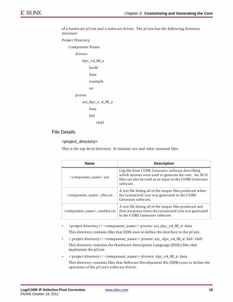
of a hardware pCore and a software driver. The pCore has the following directory structure:
Project Directory
Component Name
drivers
dpc_v4_00_a
build
data
example
src
pcores
axi_dpc_v_4_00_a
data
hdl
vhdl
File Details
<project_directory>
This is the top-level directory. It contains xco and other assorted files.
• <project directory>/<component_name>/pcores/axi_dpc_v4_00_a/data
This directory contains files that EDK uses to define the interface to the pCore.
• < project directory>/<component_name>/pcores/axi_ dpc_v4_00_a/hdl/vhdl
This directory contains the Hardware Description Language (HDL) files that implement the pCore.
• < project directory>/<component_name>/drivers/dpc_v4_00_a/data
This directory contains files that Software Development Kit (SDK) uses to define the operation of the pCore's software driver.
Name Description
<component_name>.xco
Log file from CORE Generator software describing which options were used to generate the core. An XCO files can also be used as an input to the CORE Generator software.
<component_name>_flist.txtA text file listing all of the output files produced when the customized core was generated in the CORE Generator software.
<component_name>_readme.txtA text file listing all of the output files produced and their purposes when the customized core was generated in the CORE Generator software.
LogiCORE IP Defective Pixel Correction www.xilinx.com 20PG005 October 19, 2011
Chapter 3: Customizing and Generating the Core
• < project directory>/<component_name>/drivers/dpc_v4_00_a/src
This directory contains the source code of the pCore's software dirver.
General Purpose Processor FilesWhen the interface selection is set to General Purpose Processor, CORE Generator then outputs the core as a netlist that can be inserted into a processor interface wrapper or instantiated directly in an HDL design. The output is placed in the <project directory>.
File Details
The CORE Generator software output consists of some or all the following files.
Name Description
dpc.cProvides the Application Program Interface (API) access to all features of
the Defective Pixel Correction device driver.
dpc.hProvides the API access to all features of the Defective Pixel Correction
device driver.
Name Description
<component_name>_readme.txt Readme file for the core.
<component_name>.ngc The netlist for the core.
<component_name>.veo
<component_name>.vhoThe HDL template for instantiating the core.
<component_name>.v
<component_name>.vhd The structural simulation model for the core. It is used for functionally simulatingthe core.
<component_name>.xco Log file from CORE Generator software describing which options were used togenerate the core. An XCO file can also be used as an input to the CORE Generator
software.
<component_name>_flist.txt A text file listing all of the output files produced when the customized core wasgenerated in the CORE Generator software.
<component_name>.asy IP symbol file.
<component_name>.gise ISE® software subproject files for use when including the core in ISE softwaredesigns.<component_name>.xise

LogiCORE IP Defective Pixel Correction www.xilinx.com 21PG005 October 19, 2011
Chapter 4
Designing with the Core
This chapter includes guidelines and additional information to make designing with the core easier.
General Design Guidelines
Selection of Threshold ValuesThe Xilinx Defective Pixel Correction solution provides three controls to influence the identification and monitoring of defective pixels.
Threshold value THRESH_SPATIAL_VAR defines how different a pixel needs to be from the surrounding pixels to be classified as an outlier. A practical value of 2DATA_WIDTH-5 identifies pixels that visually stand out from their surroundings. A higher threshold value for THRESH_SPATIAL_VAR results in a lower number of outlier candidates and slower convergence time for identifying all outliers, but at the same time returns fewer false positives. If heuristics for the total number of outliers (M) are known, a feedback mechanism can be implemented that tunes THRESH_SPATIAL_VAR so that the number of outlier pixels identified, num_candidates, approximates M.
Threshold value THRESH_TEMPORAL_VAR, defines the range a pixel value needs to stay in to be classified as stuck. The lower the value, the lower the chance that slowly varying pixels get characterized as stuck. However, if the sensor image is loaded with noise, or blooming may modify the readout values of dead pixels, THRESH_TEMPORAL_VAR may need to be increased to identify all stuck pixels. As a practical value for THRESH_TEMPORAL_VAR, the square root of the maximum pixel value is suggested.
Threshold value, THRESH_PIXEL_AGE, defines the number of frames presumed outliers have to hold their values within THRESH_TEMPORAL_VAR range before an outlier pixel is considered defective, and replacement (interpolation) of the pixels begin. The higher the value of THRESH_PIXEL_AGE, the less flickering due to incorrect defective pixel correction the algorithm produces, but also the longer it takes for the algorithm to converge and start replacing defective pixels. Values in the range of several thousands allow virtually no flickering while identifying outliers within minutes.
Control Signals and TimingThe propagation delay of the Defective Pixel Correction core is two full scan lines and 18 video clock cycles. The output timing signals (vblank_out, hblank_out, and active_video_out) are delayed appropriately so that the output video data is framed correctly by the timing signals. Deasserting CE suspends processing, which may be useful for data-throttling, to temporarily cease processing of a video stream to match the delay of other processing components.

LogiCORE IP Defective Pixel Correction www.xilinx.com 22PG005 October 19, 2011
Chapter 4: Designing with the Core
The control signals vblank_out, hblank_out, and active_video_out are created using a timing detector and generator within the core. The internal timing module assumes the following:
• One horizontal blanking period per row
• One vertical blanking period per frame
• Blanking signals are active high
• A minimum active frame size of eight rows and eight columns
• A minimum horizontal blanking period of two columns
• A minimum vertical blanking period of two rows
During the detection of the timing control signals, the core cannot guarantee the correct video data output. Therefore, the data output, video_data_out, of the first frame of data is set to zero even though active_video_out is high.
ClockingThe Defective Pixel Correction core has one clock "clk" that is used to clock the entire core. This includes the AXI4-Lite interface and the core logic.
ResetsThe Defective Pixel Correction core has one reset "sclr" that is used for the entire core. The reset is active-High.
Protocol DescriptionThe EDK pCore version of the Defective Pixel Correction core has an AXI4-Lite compliant processor interface
X-Ref Target - Figure 4-1
Figure 4-1: Timing Example
LogiCORE IP Defective Pixel Correction www.xilinx.com 23PG005 October 19, 2011
Chapter 5
Constraining the Core
Required ConstraintsThe clk pin should be constrained at the pixel clock rate desired for your video stream.
Device, Package, and Speed Grade SelectionsThere are no device, package or speed grade requirements for the Defective Pixel Correction core. This core has not been characterized for use in low power devices.
Clock FrequenciesThe pixel clock frequency will be the required frequency for the Defective Pixel Correction core. See Maximum Frequency in Performance in Chapter 1.
Clock ManagementThere is only one clock for the Defective Pixel Correction core.
Clock PlacementThere are no specific clock placement requirements for the Defective Pixel Correction core.
BankingThere are no specific banking rules for the Defective Pixel Correction core.
Transceiver PlacementThere are no Transceiver Placement requirements for the Defective Pixel Correction core.
I/O Standard and PlacementThere are no specific I/O standards and placement requirements for the Defective Pixel Correction core.
LogiCORE IP Defective Pixel Correction www.xilinx.com 24PG005 October 19, 2011
Chapter 6
Detailed Example Design
Directory and File ContentsThe directory structure underneath this top-level folder is described below:
• Expected
• Contains the pre-generated expected/golden data used by the testbench to compare actual output data.
• Stimuli
• Contains the pre-generated input data used by the testbench to stimulate the core (including register programming values).
• Results
• Actual output data is written to a file in this folder.
• src
• Contains the .vhd & .xco files of the core.
The .vhd file is a netlist generated using Coregen.
You can regenerate a new netlist using the .xco file in Coregen.
• tb_src
• Contains the top-level testbench design.
This directory also contains other packages used by the testbench.
• isim_wave.wcfg - Waveform configuration for ISIM
• mti_wave.do - Waveform configuration for ModelSim
• run_isim.bat - Runscript for iSim in Windows OS
• run_isim.sh - Runscript for iSim in Linux OS
• run_mti.bat - Runscript for ModelSim in Windows OS
• run_mti.sh - Runscript for ModelSim in Linux OS
Demonstration Test BenchThis demonstration test bench is provided as a simple introductory package that enables core users to observe the core generated by the CORE Generator tool operating in a waveform simulator. The user is encouraged to observe core-specific aspects in the waveform, make simple modifications to the test conditions, and observe the changes in the waveform.
LogiCORE IP Defective Pixel Correction www.xilinx.com 25PG005 October 19, 2011
Chapter 6: Detailed Example Design
Simulation• Simulation using ModelSim for Linux:
From the console, Type "source run_mti.sh".
• Simulation using ModelSim for Windows:Double click on "run_mti.bat" file.
• Simulation using iSim for Linux:From the console, Type "source run_isim.sh".
Messages and WarningsThe following warnings will appear in the console when you run one of the shell scripts:
** Warning: [9] tb_src/tb_v_spc_v4_0VHT.vhd(134): (vcom-1013) Initial value of "c_thresh_temporal_var" depends on value of signal "default_thresh_temporal_var".** Warning: [9] tb_src/tb_v_spc_v4_0VHT.vhd(141): (vcom-1013) Initial value of "c_thresh_spatial_var" depends on value of signal "default_thresh_spatial_var".** Warning: [9] tb_src/tb_v_spc_v4_0VHT.vhd(149): (vcom-1013) Initial value of "c_thresh_pixel_age" depends on value of signal "default_thresh_pixel_age".** Warning: [9] tb_src/tb_v_spc_v4_0VHT.vhd(258): (vcom-1013) Initial value of "thresh_temporal_var" depends on value of signal "default_thresh_temporal_var".** Warning: [9] tb_src/tb_v_spc_v4_0VHT.vhd(263): (vcom-1013) Initial value of "thresh_spatial_var" depends on value of signal "default_thresh_spatial_var".** Warning: [9] tb_src/tb_v_spc_v4_0VHT.vhd(267): (vcom-1013) Initial value of "thresh_pixel_age" depends on value of signal "default_thresh_pixel_age".
All of the signals do have initial values so no unknowns will be propagated through the simulation. In the Modelsim console window, you will see warnings similar to the following:
** Warning: There is an 'U'|'X'|'W'|'Z'|'-' in an arithmetic operand, there result will be 'X'(es).
The above warning is common when doing a structural simulation as the resets have not yet completely propagated. Once the resets are done, the simulation will settle and valid results will appear.
LogiCORE IP Defective Pixel Correction www.xilinx.com 26PG005 October 19, 2011
Appendix A
Verification, Compliance, and Interoperability
SimulationA highly parameterizable test bench was used to test the Defective Pixel Correction core. Testing included the following:
• Register accesses
• Processing of multiple frames of data
• Testing of various frame sizes
• Varying parameter settings
Hardware TestingThe Defective Pixel Correction core has been tested in a variety of hardware platforms at Xilinx to represent a variety of parameterizations, including the following:
• A test design was developed for the core that incorporated a MicroBlaze™ processor, AXI4-Lite interconnect and various other peripherals. The software for the test system included pre-generated input and output data along with live video stream. The MicroBlaze processor was responsible for:
• Initializing the appropriate input and output buffers
• Initializing the Color Filer Array Interpolation core.
• Launching the test.
• Comparing the output of the core against the expected results.
• Reporting the Pass/Fail status of the test and any errors that were found.

LogiCORE IP Defective Pixel Correction www.xilinx.com 27PG005 October 19, 2011
Appendix B
Migrating
Parameter Changes in the XCO FileThere are no parameter changes in the XCO file.
Port ChangesOther than an AXI4-Lite interface in place of the PLB, there are no port changes.
Functionality ChangesThere are no functionality changes to the core.
Special Considerations when Migrating to AXIThe Defective Pixel Correction core v4.0 changed from the PLB EDK pCore processor interface to the EDK pCore AXI4-Lite interface. As a result, all of the PLB-related connections have been replaced with an AXI4-Lite interface. This processor interface change does not change the functionality of the core other than an AXI4-Lite has to be used in place of the PLB.
LogiCORE IP Defective Pixel Correction www.xilinx.com 28PG005 October 19, 2011
Appendix C
Debugging
Consider the following:
• Are the input and output timing signals active_video, vblank, hblank connected?
• Is the video clock (clk) and reset (sclr) signals connected?
• Is bit 0 of the control register (BASEADDR + 0x00) set to '1'?
• Is bit 7 of the status register (BASEADDR + 0x08) set to '1'?
• Did you follow the Defective Pixel Correction Programming Flow Chart (Figure 2-3) to program the temporal, spatial and pixel age threshold registers?
See Solution Centers in Appendix F for information helpful to the debugging progress.

LogiCORE IP Defective Pixel Correction www.xilinx.com 29PG005 October 19, 2011
Appendix D
Application Software Development
Programmer's GuideA software API is provided to allow easy access to the Defective Pixel Correction pCore's registers defined in Table 2-3. To utilize the API functions provided, the following two header files must be included in the user C code:
#include "dpc.h"#include "xparameters.h"
The hardware settings of your system, including the base address of your Defective Pixel Correction core, are defined in the xparameters.h file. The dpc.h file contains the macro function definitions for controlling the Defective Pixel Correction pCore.
For examples on API function calls and integration into a user application, the drivers subdirectory of the pCore contains a file, example.c, in the dpc_v4_00_a/example subfolder. This file is a sample C program that demonstrates how to use the Defective Pixel Correction pCore API.
EDK pCore API FunctionsThis section describes the functions included in the C driver (dpc.c and dpc.h) generated for the EDK pCore API.
DPC_Enable(uint32 BaseAddress);
• This macro enables a Defective Pixel Correction instance.
• BaseAddress is the Xilinx EDK base address of the Defective Pixel Correction core (from xparameters.h).
DPC_Disable(uint32 BaseAddress);
• This macro disables a Defective Pixel Correction instance.
• BaseAddress is the Xilinx EDK base address of the Defective Pixel Correction core (from xparameters.h).
DPC_Reset(uint32 BaseAddress);
• This macro resets a Defective Pixel Correction instance. This reset effects the core immediately, and may cause image tearing.
• Reset affects the threshold registers, forces video_data_out to 0, and forces timing signal outputs to their reset state until DPC_ClearReset() is called.
LogiCORE IP Defective Pixel Correction www.xilinx.com 30PG005 October 19, 2011
Appendix D: Application Software Development
• BaseAddress is the Xilinx EDK base address of the Defective Pixel Correction core (from xparameters.h)
DPC_ClearReset(uint32 BaseAddress);
• This macro clears the reset flag of the core, which allows it to re-sync with the input video stream and return to normal operation.
• BaseAddress is the Xilinx EDK base address of the Defective Pixel Correction core (from xparameters.h).
Reading and writing pCore RegistersEach software register defined in Table 2-3 has a constant defined in dpc.h that is set to the offset for that register.
Reading a value from a register uses the base address and offset for the register:
Xuint32 value = DPC_ReadReg(XPAR_DPC_0_BASEADDR, DPC_REG03_THRESH_TEMPORAL_VAR);
This macro returns the 32-bit unsigned integer value of the register. The definition of this macro is:
DPC_ReadReg(uint32 BaseAddress, uint32 RegOffset)
• Read the given register.
• BaseAddress is the Xilinx EDK base address of the Defective Pixel Correction core (from xparameters.h).
• RegOffset is the register offset of the register (defined in Table 1).
To write to a register, use the DPC_WriteReg() function using the base address of the Defective Pixel Correction pCore instance (from xparameters.h), the offset of the desired register, and the data to write. For example:
DPC_WriteReg(XPAR_DPC_0_BASEADDR, DPC_REG03_THRESH_TEMPORAL_VAR, 1);
The definition of this macro is:
DPC_WriteReg(uint32 BaseAddress, uint32 RegOffset, uint32 Data)
• Write the given register.
• BaseAddress is the Xilinx EDK base address of the Defective Pixel Correction core (from xparameters.h).
• RegOffset is the register offset of the register (defined in Table 1).
• Data is the 32-bit value to write to the register.
DPC_RegUpdateEnable(uint32 BaseAddress);
• Calling RegUpdateEnable causes the Defective Pixel Correction to start using the updated threshold values on the next rising edge of VBlank_in. The user must manually disable the register update after a sufficient amount of time to prevent continuous updates.
• This function only works when the Defective Pixel Correction core is enabled.
• BaseAddress is the Xilinx EDK base address of the Defective Pixel Correction core (from xparameters.h)
LogiCORE IP Defective Pixel Correction www.xilinx.com 31PG005 October 19, 2011
Appendix D: Application Software Development
DPC_RegUpdateDisable(uint32 BaseAddress);
• Disabling the Register Update prevents the Defective Pixel Correction threshold registers from updating. It is recommended that the Register Update be disabled while writing to the registers in the core, until the write operation is complete. While disabled, writes to the registers are stored, but do not affect the core's behavior.
• This function only works when the Defective Pixel Correction core is enabled.
• BaseAddress is the Xilinx EDK base address of the Defective Pixel Correction core (from xparameters.h)
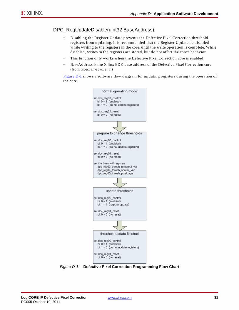
Figure D-1 shows a software flow diagram for updating registers during the operation of the core.
X-Ref Target - Figure D-1
Figure D-1: Defective Pixel Correction Programming Flow Chart
LogiCORE IP Defective Pixel Correction www.xilinx.com 32PG005 October 19, 2011
Appendix E
C Model Reference
The Xilinx® LogiCORE™ IP Defective Pixel Correction v4.0 core has a bit accurate C model designed for system modeling.
Features• Bit accurate with Defective Pixel Correction v4.0 core
• Statically linked library (.lib, .o, .obj)
• Available for 32- and 64-bit Windows and 32- and 64-bit Linux platforms
• Supports all features of the Defective Pixel Correction core that affect numerical results
• Designed for rapid integration into a larger system model
• Example C code showing how to use the function is provided
OverviewThe Xilinx LogiCORE IP Defective Pixel Correction v4.0 has a bit accurate C model for 32- and 64-bit Windows and 32- and 64-bit Linux platforms. The model has an interface consisting of a set of C functions, which reside in a statically link library (shared library). An example piece of C code showing how to call the model is provided to demonstrate the use of the C model.
The model is bit accurate, as it produces exactly the same output data as the core on a frame-by-frame basis. However the model is not cycle accurate, as it does not model the core's latency or its interface signals.
The latest version of the model is available for download on the Xilinx LogiCORE IP Defective Pixel Correction web page.
Additional Core Resources For detailed information and updates about the Defective Pixel Correction v4.0 core, see the following documents, located on the Defective Pixel Correction product page.
LogiCORE IP Defective Pixel Correction www.xilinx.com 33PG005 October 19, 2011
Appendix E: C Model Reference
Technical Support For technical support, go to www.xilinx.com/support. Questions are routed to a team with expertise using the Defective Pixel Correction v4.0 core. Xilinx provides technical support for use of this product as described in this product guide.
Xilinx cannot guarantee functionality or support of this product for designs that do not follow these guidelines.
FeedbackXilinx welcomes comments and suggestions about the Defective Pixel Correction v4.0 core and the accompanying documentation.
Defective Pixel Correction v4.0 Bit Accurate C Model and IP CoreFor comments or suggestions about the Defective Pixel Correction v4.0 core and bit accurate C model, submit a WebCase. Be sure to include the following information:
• Product name
• Core version number
• Explanation of your comments
DocumentFor comments or suggestions about the Defective Pixel Correction v4.0 core and bit accurate C model, submit a WebCase. Be sure to include the following information:
• Document title
• Document number
• Page number(s) to which your comments refer
• Explanation of your comments
Software Requirements The Defective Pixel Correction v4.0 C models were compiled and tested with the following software:
Table E-1: Compilation Tools for the Bit Accurate C Models
Platform C Compiler
32- and 64-bit Linux GCC 4.1.1
32- and 64-bit Windows Microsoft Visual Studio 2005
LogiCORE IP Defective Pixel Correction www.xilinx.com 34PG005 October 19, 2011
Appendix E: C Model Reference
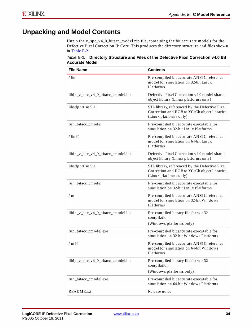
Unpacking and Model ContentsUnzip the v_spc_v4_0_bitacc_model.zip file, containing the bit accurate models for the Defective Pixel Correction IP Core. This produces the directory structure and files shown in Table E-2.
Table E-2: Directory Structure and Files of the Defective Pixel Correction v4.0 Bit Accurate Model
File Name Contents
/lin Pre-compiled bit accurate ANSI C reference model for simulation on 32-bit Linux Platforms
libIp_v_spc_v4_0_bitacc_cmodel.lib Defective Pixel Correction v4.0 model shared object library (Linux platforms only)
libstlport.so.5.1 STL library, referenced by the Defective Pixel Correction and RGB to YCrCb object libraries (Linux platforms only)
run_bitacc_cmodel Pre-compiled bit accurate executable for simulation on 32-bit Linux Platforms
/lin64 Pre-compiled bit accurate ANSI C reference model for simulation on 64-bit Linux Platforms
libIp_v_spc_v4_0_bitacc_cmodel.lib Defective Pixel Correction v4.0 model shared object library (Linux platforms only)
libstlport.so.5.1 STL library, referenced by the Defective Pixel Correction and RGB to YCrCb object libraries (Linux platforms only)
run_bitacc_cmodel Pre-compiled bit accurate executable for simulation on 32-bit Linux Platforms
/nt Pre-compiled bit accurate ANSI C reference model for simulation on 32-bit Windows Platforms
libIp_v_spc_v4_0_bitacc_cmodel.lib Pre-compiled library file for win32 compilation
(Windows platforms only)
run_bitacc_cmodel.exe Pre-compiled bit accurate executable for simulation on 32-bit Windows Platforms
/nt64 Pre-compiled bit accurate ANSI C reference model for simulation on 64-bit Windows Platforms
libIp_v_spc_v4_0_bitacc_cmodel.lib Pre-compiled library file for win32 compilation
(Windows platforms only)
run_bitacc_cmodel.exe Pre-compiled bit accurate executable for simulation on 64-bit Windows Platforms
README.txt Release notes

LogiCORE IP Defective Pixel Correction www.xilinx.com 35PG005 October 19, 2011
Appendix E: C Model Reference
InstallationOn Linux, ensure that the directory in which the files libIp_v_spc_v4_0_bitacc_cmodel.so and libstlport.so.5.1 are located is in your $LD_LIBRARY_PATH environment variable.
Defective Pixel Correction v4.0 Bit Accurate C ModelThe bit-accurate C model is accessed through a set of functions and data structures, declared in the header file v_spc_v4_0_bitacc_cmodel.h.
Before using the model, the structures holding the inputs, generics and output of the Defective Pixel Correction instance have to be defined:
struct xilinx_ip_v_spc_v4_0_generics spc_generics;struct xilinx_ip_v_spc_v4_0_inputs spc_inputs;struct xilinx_ip_v_spc_v4_0_outputs spc_outputs;
Declaration of the preceding structs can be found in v_spc_v4_0_bitacc_cmodel.h.
The two generic parameters the Defective Pixel Correction v4.0 IP Core bit accurate model takes are shown in Table E-3:
pg005_v_spc.pdf The Defective Pixel Correction Core Product Guide
v_spc_v4_0_bitacc_cmodel.h Model header file
rgb_utils.h Header file declaring the RGB image / video container type and support functions
bmp_utils.h Header file declaring the bitmap (.bmp) image file I/O functions
video_utils.h Header file declaring the generalized image / video container type, I/O and support functions.
instrument.bmp 128x128 example image provided with C model
run_bittacc_model.c Example code calling the C model
Table E-2: Directory Structure and Files of the Defective Pixel Correction v4.0 Bit Accurate Model (Cont’d)
File Name Contents
Table E-3: Member Variables of the Generics Structure
Type NameDefault Value
Function
int C_DATA_WIDTH 8 CORE Generator™ software “Data Width” parameter. Allowed values are 8,10 and 12.
int C_STATUS_WIDTH 10 log2 of the maximum number of defective pixels GUI parameter.

LogiCORE IP Defective Pixel Correction www.xilinx.com 36PG005 October 19, 2011
Appendix E: C Model Reference
Calling
int xilinx_ip_v_spc_v4_0_get_default_generics(struct xilinx_ip_v_spc_v4_0_generics *generics)
initializes the generics structure according to Table E-4.
The structure stats_inputs defines run time parameters and the actual input image. The structure holds the following members:
int xilinx_ip_v_spc_v4_0_get_default_inputs( struct xilinx_ip_v_spc_v4_0_generics *generics, struct xilinx_ip_v_spc_v4_0_inputs *inputs)
initializes members of the input structure with zeroes. No memory is allocated for the video_in structure or the integer vectors in inputs.
Note: NOTE: The video_in variable is not initialized, as the initialization depends on the actual test image to be simulated. The next chapter describes the initialization of the video_in structure.
Note: NOTE: The thresh_spatial_var, thresh_temporal_var and thresh_pixel_age vectors are not allocated or initialized by xilinx_ip_v_spc_v4_0_get_default_inputs().
After the inputs are defined the model can be simulated by calling the function
int xilinx_ip_v_spc_v4_0_bitacc_simulate(struct xilinx_ip_v_spc_v4_0_generics* generics,struct xilinx_ip_v_spc_v4_0_inputs* inputs,struct xilinx_ip_v_spc_v4_0_outputs* outputs).
Results are provided in the outputs structure, which contains only one member, type video_struct.
int DEFAULT_THRESH_PIXEL_AGE 1200 Initialization value applied to the thresh_pixel_age input of the core.
int DEFAULT_THRESH_SPATIAL_VAR 6554 Initialization value applied to the thresh_spatial_var input of the core.
int DEFAULT_THRESH_TEMPORAL_VAR 2 Initialization value applied to the thresh_temporal_var input of the core.
Table E-4: Member Variables of the Input Structure
Type Name Function
video_struct video_in Holds the input video stream (can contain multiple frames)
int* thresh_spatial_var Pointer to integer vector containing spatial variance threshold values per frame simulated
int* thresh_temporal_var Pointer to integer vector containing temporal variance threshold values per frame simulated
int* thresh_pixel_age Pointer to integer vector containing pixel age threshold values per frame simulated
Table E-3: Member Variables of the Generics Structure

LogiCORE IP Defective Pixel Correction www.xilinx.com 37PG005 October 19, 2011
Appendix E: C Model Reference
After the outputs were evaluated and/or saved, dynamically allocated memory for input and output video structures must be released by calling function
void xilinx_ip_v_spc_v4_0_destroy(struct xilinx_ip_v_spc_v4_0_inputs *input, struct xilinx_ip_v_spc_v4_0_outputs *output).
Successful execution of all provided functions except for the destroy function return a value 0, otherwise a non-zero error code indicates that problems were encountered during function calls.
Defective Pixel Correction Input and Output Video StructureInput images or video streams can be provided to the Defective Pixel Correction v4.0 reference model using the video_struct structure, defined in video_utils.h:
struct video_struct{ int frames, rows, cols, bits_per_component, mode; uint16*** data[5]; };
Table E-5: Member Variables of the Video Structure
Member Variable Designation
Frames Number of video/image frames in the data structure
Pertaining to the image plane with the most rows and columns, such as the luminance channel for yuv data. Frame dimensions are assumed constant through all frames of the video stream; however, different planes, such as y,u and v may have different dimensions.
Rows Number of rows per frame
Pertaining to the image plane with the most rows and columns, such as the luminance channel for yuv data. Frame dimensions are assumed constant through all frames of the video stream; however, different planes, such as y,u and v may have different dimensions.
Cols Number of columns per frame
Pertaining to the image plane with the most rows and columns, such as the luminance channel for yuv data. Frame dimensions are assumed constant through all frames of the video stream; however, different planes, such as y,u and v may have different dimensions.
bits_per_component Number of bits per color channel / component.
All image planes are assumed to have the same color/component representation. Maximum number of bits per component is 16.
Mode Contains information about the designation of data planes.
Named constants to be assigned to mode are listed in Table E-6.
data Set of 5 pointers to 3 dimensional arrays containing data for image planes.
data is in 16 bit unsigned integer format accessed as data[plane][frame][row][col].
LogiCORE IP Defective Pixel Correction www.xilinx.com 38PG005 October 19, 2011
Appendix E: C Model Reference
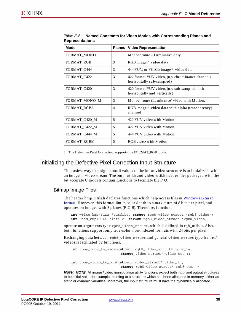
1. The Defective Pixel Correction supports the FORMAT_RGB mode.
Initializing the Defective Pixel Correction Input StructureThe easiest way to assign stimuli values to the input video structure is to initialize it with an image or video stream. The bmp_util.h and video_util.h header files packaged with the bit accurate C models contain functions to facilitate file I/O.
Bitmap Image Files
The header bmp_utils.h declares functions which help access files in Windows Bitmap format. However, this format limits color depth to a maximum of 8 bits per pixel, and operates on images with 3 planes (R,G,B). Therefore, functions
int write_bmp(FILE *outfile, struct rgb8_video_struct *rgb8_video);int read_bmp(FILE *infile, struct rgb8_video_struct *rgb8_video);
operate on arguments type rgb8_video_struct, which is defined in rgb_utils.h. Also, both functions support only true-color, non-indexed formats with 24 bits per pixel.
Exchanging data between rgb8_video_struct and general video_struct type frames/videos is facilitated by functions:
int copy_rgb8_to_video(struct rgb8_video_struct* rgb8_in, struct video_struct* video_out );
int copy_video_to_rgb8(struct video_struct* video_in, struct rgb8_video_struct* rgb8_out );
Note: NOTE: All image / video manipulation utility functions expect both input and output structures to be initialized -- for example, pointing to a structure which has been allocated in memory, either as static or dynamic variables. Moreover, the input structure must have the dynamically allocated
Table E-6: Named Constants for Video Modes with Corresponding Planes and Representations
Mode Planes Video Representation
FORMAT_MONO 1 Monochrome – Luminance only.
FORMAT_RGB 3 RGB image / video data
FORMAT_C444 3 444 YUV, or YCrCb image / video data
FORMAT_C422 3 422 format YUV video, (u,v chrominance channels horizontally sub-sampled)
FORMAT_C420 3 420 format YUV video, (u,v sub-sampled both horizontally and vertically)
FORMAT_MONO_M 3 Monochrome (Luminance) video with Motion.
FORMAT_RGBA 4 RGB image / video data with alpha (transparency) channel
FORMAT_C420_M 5 420 YUV video with Motion
FORMAT_C422_M 5 422 YUV video with Motion
FORMAT_C444_M 5 444 YUV video with Motion
FORMAT_RGBM 5 RGB video with Motion
LogiCORE IP Defective Pixel Correction www.xilinx.com 39PG005 October 19, 2011
Appendix E: C Model Reference
container (data[] or r[],g[],b[]) structures already allocated and initialized with the input frame(s). If the output container structure is pre-allocated at the time of the function call, the utility functions verify and throw an error if the output container size does not match the size of the expected output. If the output container structure is not pre-allocated, the utility functions create the appropriate container to hold results.
Binary Image/Video Files
The header video_utils.h declares functions which help load and save generalized video files in raw, uncompressed format. Functions
int read_video( FILE* infile, struct video_struct* in_video);
int write_video(FILE* outfile, struct video_struct* out_video);
effectively serialize the video_struct structure. The corresponding file contains a small, plain text header defining, "Mode", "Frames", "Rows", "Columns", and "Bits per Pixel". The plain text header is followed by binary data, 16 bits per component in scan line continuous format. Subsequent frames contain as many component planes as defined by the video mode value selected. Also, the size (rows, columns) of component planes may differ within each frame as defined by the actual video mode selected.
Working with video_struct Containers
Header file video_utils.h defines functions to simplify access to video data in video_struct.
int video_planes_per_mode(int mode);int video_rows_per_plane(struct video_struct* video, int plane);int video_cols_per_plane(struct video_struct* video, int plane);
Function video_planes_per_mode returns the number of component planes defined by the mode variable, as described in Table E-6. Functions video_rows_per_plane and video_cols_per_plane return the number of rows and columns in a given plane of the selected video structure. The following example demonstrates using these functions in conjunction to process all pixels within a video stream stored in variable in_video, with the following construct:
for (int frame = 0; frame < in_video->frames; frame++) { for (int plane = 0; plane < video_planes_per_mode(in_video->mode); plane++) { for (int row = 0; row < rows_per_plane(in_video,plane); row++) { for (int col = 0; col < cols_per_plane(in_video,plane); col++) {
// User defined pixel operations on // in_video->data[plane][frame][row][col]
} } }}
Destroy the Video Structure
Finally, the video structure must be destroyed to free up memory used to store the video structure.

LogiCORE IP Defective Pixel Correction www.xilinx.com 40PG005 October 19, 2011
Appendix E: C Model Reference
C Model Example CodeAn example C file, run_bitacc_cmodel.c, is provided to demonstrate the steps required to use the model. Follow the compilation instructions to run the example executable.
The structure of the example C code provided is as follows. The main() function reads command line parameters, parses them, and passes them as arguments to the bmp_processing() function.
If invoked with insufficient parameters, the following help message is printed:
Usage: run_bitacc_cmodel input_file stim_path result_path data_width M N in_file : name of the input BMP file without pathstim_path : Full or partial path to the input BMP file
Stimuli BMP and TXT files will be placed here also under a directory created with the same name as the input file
result_path : Full or partial path to the output golden_result filesGolden Result BMP and TXT files will be placed undera directory created here with the same name as the input
file.data_width : The number of bits in the output data representation.M : the number of stuck pixels to be insertedN : number of stimuli / golden result frames to be generated
To demonstrate the Defective Pixel Correction Core and corresponding bit-true C model, a video sequence corrupted by defective pixels is necessary. The bmp_processing() function first generates this stimuli.
The input bitmap image is circularly translated in a direction specified by variables dx and dx (line 160), creating a total number of N frames, N specified as a command-line parameter. To simulate defective pixels, on each stimuli frame M pixels are corrupted. The location and intensity of defective pixels is randomized (line 211).
The bmp format encodes pixels using 24 bits per pixel; however, the Defective Pixel Correction Core operates on Bayer-sub sampled, 8, 10 or 12 bit samples. Therefore, each stimuli frame is Bayer sub-sampled, and if needed the color representation is converted to data_width bits by bit-shifting and assigning a fixed pattern value to the LSBs (line 251).
The C model example stores all stimuli and result frames as individual bitmap files in separate directories. Both directories share the name of the input image (in_file) without extension. The stimuli directory location is specified by the command-line parameter stim_path, the result directory location is specified by the command-line parameter result_path. If the directories do not exist, function create_dirs() creates them, if they already exists, contents are cleared before stimuli/result generation.
If the specified input bmp file was opened successfully, the stimuli directory is populated with the input N stimuli frames saved as bmp files. For HDL testing purposes, a plain text (.txt) file is also created, which contains the input video stream (all frames concatenated) in a human-readable, one pixel / line format.
Core input threshold values, which can change on a frame-by-frame basis, are set up by the demonstrator C model to remain constant for the entire length of the simulation (line 186). The spatial and temporal thresholds are initialized to default values, 6554 and 2 respectively. The pixel age threshold, which controls the minimum number of frames through which non-changing, outlier pixels have to hold their values in order to be interpolated by the Defective Pixel Correction algorithm, are initialized to N/2, half the number of frames to simulate.
LogiCORE IP Defective Pixel Correction www.xilinx.com 41PG005 October 19, 2011
Appendix E: C Model Reference
After successful execution of the C model (line 290), the results directory is populated with N resulting frames saved as bmp files. For HDL testing purposes, a plain text (.txt) file is also created, which contains the output video stream (all frames concatenated) in a human-readable, one pixel / line format.
Compiling the Example with the Defective Pixel Correction C Model
Linux (32- and 64-bit)To compile the example code, first ensure that the directory in which the files libIp_v_spc_v4_0_bitacc_cmodel.so and libstlport.so.5.1 are located is present in your $LD_LIBRARY_PATH environment variable. These shared libraries are referenced during the compilation and linking process. Then cd into the directory where the header files, the library files and run_bitacc_cmodel.c were unpacked. The libraries and header files are referenced during the compilation and linking process.
Place the header file and C source file in a single directory. Then in that directory, compile using the GNU C Compiler:
gcc -m32 -x c++ ../run_bitacc_cmodel.c ../parsers.c -o run_bitacc_cmodel -L. -lIp_v_spc_v4_0_bitacc_cmodel -Wl,-rpath,.
gcc –m64 -x c++ ../run_bitacc_cmodel.c ../parsers.c -o run_bitacc_cmodel -L. -lIp_v_spc_v4_0_bitacc_cmodel -Wl,-rpath,.
Windows (32- and 64-bit) Precompiled library v_spc_v4_0_bitacc_cmodel.lib and top-level demonstration code run_bitacc_cmodel.c should be compiled with an ANSI C compliant compiler under Windows. Here an example is presented using Microsoft Visual Studio.
In Visual Studio create a new, empty Win32 Console Application project. As existing items, add:
• libIpv_spc_v4_0_bitacc_cmodel.lib to the "Resource Files" folder of the project,
• run_bitacc_cmodel.c to the "Source Files" folder of the project,
• v_spc_v4_0_bitacc_cmodel.h header files to "Header Files" folder of the project (optional),
After the project has been created and populated, it needs to be compiled and linked (built) in order to create a win32 executable. To perform the build step, choose "Build Solution" from the Build menu. An executable matching the project name has been created either in the Debug or Release subdirectories under the project location based on whether "Debug" or "Release" has been selected in the "Configuration Manager" under the Build menu.
Running the Example, Evaluating ResultsFor a quick look at the effects of the Defective Pixel Correction algorithm, an input image, instrument.bmp, stimuli and results directories are provided in the C model package. Command
./run_bitacc_cmodel instrument.bmp stimuli results 8 30 10

LogiCORE IP Defective Pixel Correction www.xilinx.com 42PG005 October 19, 2011
Appendix E: C Model Reference
runs the C model demonstrator, creates 10 stimuli and result frames in the respective directories under stimuli/instrument and results/instrument with 30 defective pixels inserted into the 8-bit/sample stimuli data.
Looking at result frame 0000 shows that all of the defective pixels are still present, whereas on frame 0005, defective pixels, which are visual outliers have been removed. Some defective pixels, which are situated close to edges, or small, high-contrast objects may not be identified as outliers yet. Running the simulation longer, or changing the translation vector in the demonstrator to vertical shift will result to identification and interpolation of all defective pixels.
LogiCORE IP Defective Pixel Correction www.xilinx.com 43PG005 October 19, 2011
Appendix F
Additional Resources
Xilinx ResourcesFor support resources such as Answers, Documentation, Downloads, and Forums, see the Xilinx Support website at:
http://www.xilinx.com/support.
For a glossary of technical terms used in Xilinx documentation, see:
http://www.xilinx.com/support/documentation/sw_manuals/glossary.pdf.
Solution CentersSee the Xilinx Solution Centers for support on devices, software tools, and intellectual property at all stages of the design cycle. Topics include design assistance, advisories, and troubleshooting tips.
ReferencesThese documents provide supplemental material useful with this user guide.
1. AXI Reference Guide.
Technical SupportXilinx provides technical support at www.xilinx.com/support for this LogiCORE™ IP product when used as described in the product documentation. Xilinx cannot guarantee timing, functionality, or support of product if implemented in devices that are not defined in the documentation, if customized beyond that allowed in the product documentation, or if changes are made to any section of the design labeled DO NOT MODIFY.
See the IP Release Notes Guide (XTP025) for more information on this core. For each core, there is a master Answer Record that contains the Release Notes and Known Issues list for the core being used. The following information is listed for each version of the core:
• New Features
• Resolved Issues
• Known Issues
LogiCORE IP Defective Pixel Correction www.xilinx.com 44PG005 October 19, 2011
Appendix F: Additional Resources
Ordering InformationThe Defective Pixel Correction core is provided under the Xilinx Core License Agreement and can be generated using the Xilinx® CORE Generator™ system. The CORE Generator system is shipped with Xilinx ISE® Design Suite software.
A simulation evaluation license for the core is shipped with the CORE Generator system. To access the full functionality of the core, including FPGA bitstream generation, a full license must be obtained from Xilinx. For more information, visit the product page for this core.
Contact your local Xilinx sales representative for pricing and availability of additional Xilinx LogiCORE IP modules and software. Information about additional Xilinx LogiCORE IP modules is available on the Xilinx IP Center.
Revision HistoryThe following table shows the revision history for this document.
Notice of DisclaimerThe information disclosed to you hereunder (the “Materials”) is provided solely for the selection and use of Xilinx products. To the maximum extent permitted by applicable law: (1) Materials are made available “AS IS” and with all faults, Xilinx hereby DISCLAIMS ALL WARRANTIES AND CONDITIONS, EXPRESS, IMPLIED, OR STATUTORY, INCLUDING BUT NOT LIMITED TO WARRANTIES OF MERCHANTABILITY, NON-INFRINGEMENT, OR FITNESS FOR ANY PARTICULAR PURPOSE; and (2) Xilinx shall not be liable (whether in contract or tort, including negligence, or under any other theory of liability) for any loss or damage of any kind or nature related to, arising under, or in connection with, the Materials (including your use of the Materials), including for any direct, indirect, special, incidental, or consequential loss or damage (including loss of data, profits, goodwill, or any type of loss or damage suffered as a result of any action brought by a third party) even if such damage or loss was reasonably foreseeable or Xilinx had been advised of the possibility of the same. Xilinx assumes no obligation to correct any errors contained in the Materials or to notify you of updates to the Materials or to product specifications. You may not reproduce, modify, distribute, or publicly display the Materials without prior written consent. Certain products are subject to the terms and conditions of the Limited Warranties which can be viewed at http://www.xilinx.com/warranty.htm; IP cores may be subject to warranty and support terms contained in a license issued to you by Xilinx. Xilinx products are not designed or intended to be fail-safe or for use in any application requiring fail-safe performance; you assume sole risk and liability for use of Xilinx products in Critical Applications: http://www.xilinx.com/warranty.htm#critapps.
© Copyright 2011 Xilinx, Inc. Xilinx, the Xilinx logo, Artix, ISE, Kintex, Spartan, Virtex, Zynq, and other designated brands included herein are trademarks of Xilinx in the United States and other countries. All other trademarks are the property of their respective owners.
Date Version Revision
10/19/2011 1.0 Initial Xilinx release.


![SCIENTIFIC PROGRAMME - senc.es · Instituto de Neurociencias (UMH-CSIC) EPIGENOMIC CORRECTION OF DEFECTIVE PLASTICITY [AND MEMORY FORMATION] IN A MOUSE MODEL OF TAUOPATHY WITH AN](https://static.documents.pub/doc/80x56/5bf5bb8809d3f237308c0ff6/scientific-programme-sences-instituto-de-neurociencias-umh-csic-epigenomic.jpg)


