416
Vivado Design Suite 7 Series FPGA Libraries Guide UG953 (v 2012.2) July 25, 2012

Vivado Design Suite 7 Series FPGALibraries Guide
UG953 (v 2012.2) July 25, 2012

Notice of Disclaimer
The information disclosed to you hereunder (the "Materials") is provided solely for the selection and useof Xilinx products. To the maximum extent permitted by applicable law: (1) Materials are made available"AS IS" and with all faults, Xilinx hereby DISCLAIMS ALL WARRANTIES AND CONDITIONS, EXPRESS,IMPLIED, OR STATUTORY, INCLUDING BUT NOT LIMITED TO WARRANTIES OF MERCHANTABILITY,NON-INFRINGEMENT, OR FITNESS FOR ANY PARTICULAR PURPOSE; and (2) Xilinx shall not be liable(whether in contract or tort, including negligence, or under any other theory of liability) for any loss ordamage of any kind or nature related to, arising under, or in connection with, the Materials (includingyour use of the Materials), including for any direct, indirect, special, incidental, or consequential loss ordamage (including loss of data, profits, goodwill, or any type of loss or damage suffered as a result ofany action brought by a third party) even if such damage or loss was reasonably foreseeable or Xilinxhad been advised of the possibility of the same. Xilinx assumes no obligation to correct any errorscontained in the Materials or to notify you of updates to the Materials or to product specifications.You may not reproduce, modify, distribute, or publicly display the Materials without prior writtenconsent. Certain products are subject to the terms and conditions of the Limited Warranties which canbe viewed at http://www.xilinx.com/warranty.htm; IP cores may be subject to warranty and supportterms contained in a license issued to you by Xilinx. Xilinx products are not designed or intended to befail-safe or for use in any application requiring fail-safe performance; you assume sole risk and liabilityfor use of Xilinx products in Critical Applications: http://www.xilinx.com/warranty.htm#critapps.
© Copyright 2002-2012 Xilinx Inc. All rights reserved. Xilinx, the Xilinx logo, Artix, ISE, Kintex, Spartan,Virtex, Zynq, and other designated brands included herein are trademarks of Xilinx in the United Statesand other countries. All other trademarks are the property of their respective owners.
Vivado Design Suite 7 Series FPGA Libraries GuideUG953 (v 2012.2) July 25, 2012 www.xilinx.com 2
Chapter 1
Introduction
OverviewThis HDL guide is part of the Vivado™ Design Suite documentation collection. A separateversion of this guide is available if you prefer to work with schematics.
This guide contains the following:
• Introduction.
• A list of design elements supported in this architecture, organized by functionalcategories.
• Descriptions of each available primitive.
About Design ElementsThis version of the Libraries Guide describes the valid design elements for 7 Series architecturesincluding Zynq™, and includes examples of instantiation code for each element. Instantiationtemplates are also supplied in a separate ZIP file, which you can find on www.xilinx.com linkedto this file.
Design elements are divided into the following main categories:
• Macros : These elements are in the UniMacro library in the tool, and are used toinstantiate primitives that are complex to instantiate by just using the primitives. Thesynthesis tools will automatically expand the unimacros to their underlying primitives.
• Primitives: Xilinx components that are native to the architecture you are targeting.If you instantiate a primitive in your design, after the translation process (ngdbuild)you will end up with the exact same component in the back end. For example, if youinstantiate the Virtex®-5 element known as ISERDES_NODELAY as a user primitive, afteryou run translate (ngdbuild) you will end up with an ISERDES_NODELAY in the back endas well. If you were using ISERDES in a Virtex-5 device, then this will automaticallyretarget to an ISERDES_NODELAY for Virtex-5 in the back end. Hence, this concept of a“primitive” differs from other uses of that term in this technology.
CORE Generator maintains software libraries with hundreds of functional design elements(UniMacros and primitives) for different device architectures. New functional elementsare assembled with each release of development system software. In addition to acomprehensive Unified Library containing all design elements, this guide is one in a series ofarchitecture-specific libraries.
Vivado Design Suite 7 Series FPGA Libraries GuideUG953 (v 2012.2) July 25, 2012 www.xilinx.com 3

Introduction
Design Entry MethodsFor each design element in this guide, Xilinx evaluates four options for using the designelement, and recommends what we believe is the best solution for you. The four options are:
• Instantiation: This component can be instantiated directly into the design. This methodis useful if you want to control the exact placement of the individual blocks.
• Inference: This component can be inferred by most supported synthesis tools. Youshould use this method if you want to have complete flexibility and portability of thecode to multiple architectures. Inference also gives the tools the ability to optimize forperformance, area, or power, as specified by the user to the synthesis tool.
• Coregen & Wizards: This component can be used through CORE Generator or otherWizards. You should use this method if you want to build large blocks of any FPGAprimitive that cannot be inferred. When using this flow, you will have to re-generateyour cores for each architecture that you are targeting.
• Macro Support: This component has a UniMacro that can be used. These componentsare in the UniMacro library in the Xilinx tool, and are used to instantiate primitives thatare too complex to instantiate by just using the primitives. The synthesis tools willautomatically expand UniMacros to their underlying primitives.
Vivado Design Suite 7 Series FPGA Libraries GuideUG953 (v 2012.2) July 25, 2012 www.xilinx.com 4

Chapter 2
Unimacros
OverviewThis section describes the unimacros that can be used with 7 Series architectures includingZynq™. The unimacros are organized alphabetically.
The following information is provided for each unimacro, where applicable:
• Name of element
• Brief description
• Schematic symbol
• Logic table (if any)
• Port descriptions
• Design Entry Method
• Available attributes
• Example instantiation code
• For more information
Vivado Design Suite 7 Series FPGA Libraries GuideUG953 (v 2012.2) July 25, 2012 www.xilinx.com 5

Unimacros
BRAM_SDP_MACROMacro: Simple Dual Port RAM
Introduction7 series FPGA devices contain several block RAM memories that can be configured asgeneral-purpose 36Kb or 18Kb RAM/ROM memories. These block RAM memories offer fastand flexible storage of large amounts of on-chip data. Both read and write operations are fullysynchronous to the supplied clock(s) of the component. However, READ and WRITE ports canoperate fully independently and asynchronously to each other, accessing the same memoryarray. Byte-enable write operations are possible, and an optional output register can be used toreduce the clock-to-out times of the RAM.
Note This element must be configured so that read and write ports have the same width.
Vivado Design Suite 7 Series FPGA Libraries GuideUG953 (v 2012.2) July 25, 2012 www.xilinx.com 6

Unimacros
Port DescriptionName Direction Width (Bits) Function
DO Output See Configuration Table Data output bus addressed by RDADDR.
DI Input See Configuration Table Data input bus addressed by WRADDR.
WRADDR,RDADDR
Input See Configuration Table Write/Read address input buses.
WE Input See Configuration Table Byte-Wide Write enable.
WREN,RDEN
Input 1 Write/Read enable
SSR Input 1 Output registers synchronous reset.
REGCE Input 1 Output register clock enable input (validonly when DO_REG=1).
WRCLK,RDCLK
Input 1 Write/Read clock input.
Port ConfigurationThis unimacro is a parameterizable version of the primitive, and can be instantiated only. Usethis table to correctly configure the unimacro to meet design needs.
DATA_WIDTH BRAM_SIZE ADDR WE
72 - 37 36Kb 9 8
36Kb 1036 - 19
18Kb 9
4
36Kb 1118 - 10
18Kb 10
2
36Kb 129 - 5
18Kb 11
1
36Kb 134 - 3
18Kb 12
1
36Kb 142
18Kb 13
1
36Kb 151
18Kb 14
1
Design Entry MethodThis unimacro is a parameterizable version of the primitive, and can be instantiated only. Consultthe Port Configuration section to correctly configure this element to meet your design needs.
Vivado Design Suite 7 Series FPGA Libraries GuideUG953 (v 2012.2) July 25, 2012 www.xilinx.com 7

Unimacros
Instantiation Yes
Inference No
CORE Generator™ and wizards No
Macro support Recommended
Available AttributesAttribute Data Type Allowed Values Default Description
BRAM_SIZE String "36Kb", "18Kb" "18Kb" Configures RAM as "36Kb" or"18Kb" memory.
DEVICE String "7SERIES" "7SERIES" Target hardware architecture.
DO_REG Integer 0, 1 0 A value of 1 enables to theoutput registers to the RAMenabling quicker clock-to-outfrom the RAM at the expenseof an added clock cycle of readlatency. A value of 0 allows aread in one clock cycle but willhave slower clock to out timing.
INIT Hexadecimal Any 72-Bit Value All zeros Specifies the initial value on theoutput after configuration.
READ_WIDTH,WRITE_WIDTH
Integer 1-72 36 Specifies the size of the DI andDO buses.
The following combinations areallowed:
• READ_WIDTH =WRITE_WIDTH
• If asymmetric,READ_WIDTH andWRITE_WIDTH mustbe in the ratio of 2, ormust be values allowedby the unisim (1, 2, 4, 8,9, 16, 18, 32, 36, 64, 72)
INIT_FILE String Stringrepresentingfile name andlocation.
NONE Name of the file containing initialvalues.
Vivado Design Suite 7 Series FPGA Libraries GuideUG953 (v 2012.2) July 25, 2012 www.xilinx.com 8

Unimacros
Attribute Data Type Allowed Values Default Description
SIM_COLLISION_CHECK
String "ALL","WARNING_ONLY","GENERATE_X_ONLY","NONE"
"ALL" Allows modification of thesimulation behavior if a memorycollision occurs. The output isaffected as follows:
• "ALL" - Warningproduced and affectedoutputs/memorylocation go unknown(X).
• "WARNING_ONLY" -Warning producedand affectedoutputs/memory retainlast value.
• "GENERATE_X_ONLY"- No warning.However, affectedoutputs/memory gounknown (X).
• "NONE" - Nowarning and affectedoutputs/memory retainlast value.
Note Setting this to a value otherthan "ALL" can allow problems inthe design go unnoticed duringsimulation. Care should be takenwhen changing the value ofthis attribute. Please see theSynthesis and Simulation DesignGuide for more information.
SRVAL Hexadecimal Any 72-Bit Value All zeroes Specifies the output value of onthe DO port upon the assertionof the synchronous reset (RST)signal.
INIT_00 toINIT_7F
Hexadecimal Any 256-Bit Value All zeroes Allows specification of the initialcontents of the 16Kb or 32Kbdata memory array.
INITP_00 toINITP_0F
Hexadecimal Any 256-Bit Value All zeroes Allows specification of the initialcontents of the 2Kb or 4Kb paritydata memory array.
VHDL Instantiation TemplateUnless they already exist, copy the following two statements and paste them before the entitydeclaration.Library UNISIM;use UNISIM.vcomponents.all;
-- BRAM_SDP_MACRO:Simple Dual Port RAM-- 7 Series-- Xilinx HDL Libraries Guide, version 2012.2
Vivado Design Suite 7 Series FPGA Libraries GuideUG953 (v 2012.2) July 25, 2012 www.xilinx.com 9

Unimacros
-- Note - This Unimacro model assumes the port directions to be "downto".-- Simulation of this model with "to" in the port directions could lead to erroneous results.
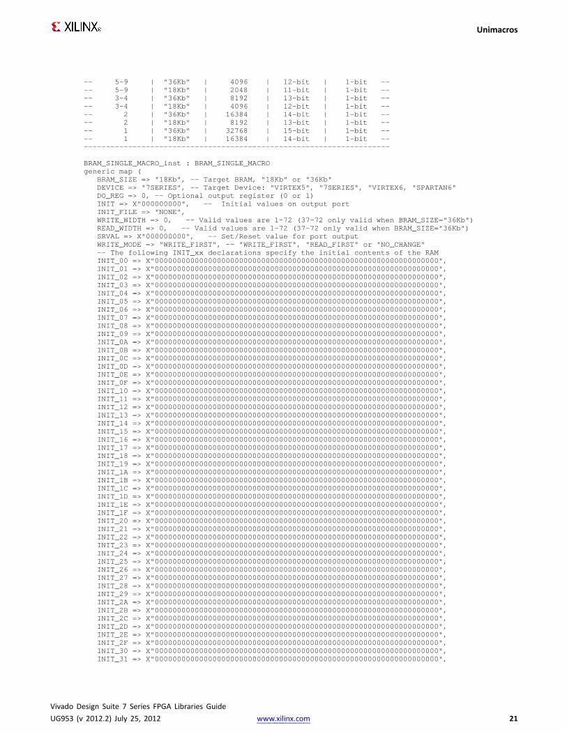
------------------------------------------------------------------------- READ_WIDTH| BRAM_SIZE | READ Depth | RDADDRWidth | ---- WRITE_WIDTH | | WRITE Depth | WRADDRWidth | WEWidth ---- ============|===========|=============|==============|============---- 37-72 | "36Kb" | 512 | 9-bit | 8-bit ---- 19-36 | "36Kb" | 1024 | 10-bit | 4-bit ---- 19-36 | "18Kb" | 512 | 9-bit | 4-bit ---- 10-18 | "36Kb" | 2048 | 11-bit | 2-bit ---- 10-18 | "18Kb" | 1024 | 10-bit | 2-bit ---- 5-9 | "36Kb" | 4096 | 12-bit | 1-bit ---- 5-9 | "18Kb" | 2048 | 11-bit | 1-bit ---- 3-4 | "36Kb" | 8192 | 13-bit | 1-bit ---- 3-4 | "18Kb" | 4096 | 12-bit | 1-bit ---- 2 | "36Kb" | 16384 | 14-bit | 1-bit ---- 2 | "18Kb" | 8192 | 13-bit | 1-bit ---- 1 | "36Kb" | 32768 | 15-bit | 1-bit ---- 1 | "18Kb" | 16384 | 14-bit | 1-bit -------------------------------------------------------------------------
BRAM_SDP_MACRO_inst : BRAM_SDP_MACROgeneric map (
BRAM_SIZE => "18Kb", -- Target BRAM, "18Kb" or "36Kb"DEVICE => "7SERIES", -- Target device: "VIRTEX5", "VIRTEX6", "7SERIES", "SPARTAN6"WRITE_WIDTH=> 0, -- Valid values are 1-72 (37-72 only valid when BRAM_SIZE="36Kb")READ_WIDTH=> 0, -- Valid values are 1-72 (37-72 only valid when BRAM_SIZE="36Kb")DO_REG=> 0, -- Optional output register (0 or 1)INIT_FILE => "NONE",SIM_COLLISION_CHECK => "ALL", -- Collision check enable "ALL", "WARNING_ONLY",
-- "GENERATE_X_ONLY"or "NONE"SRVAL => X"000000000000000000", -- Set/Reset value for port outputWRITE_MODE=> "WRITE_FIRST", -- Specify "READ_FIRST" for same clock or synchronous clocks
-- Specify "WRITE_FIRST for asynchrononous clocks on portsINIT => X"000000000000000000", -- Initial values on output port-- The following INIT_xx declarations specify the initial contents of the RAMINIT_00 => X"0000000000000000000000000000000000000000000000000000000000000000",INIT_01 => X"0000000000000000000000000000000000000000000000000000000000000000",INIT_02 => X"0000000000000000000000000000000000000000000000000000000000000000",INIT_03 => X"0000000000000000000000000000000000000000000000000000000000000000",INIT_04 => X"0000000000000000000000000000000000000000000000000000000000000000",INIT_05 => X"0000000000000000000000000000000000000000000000000000000000000000",INIT_06 => X"0000000000000000000000000000000000000000000000000000000000000000",INIT_07 => X"0000000000000000000000000000000000000000000000000000000000000000",INIT_08 => X"0000000000000000000000000000000000000000000000000000000000000000",INIT_09 => X"0000000000000000000000000000000000000000000000000000000000000000",INIT_0A => X"0000000000000000000000000000000000000000000000000000000000000000",INIT_0B => X"0000000000000000000000000000000000000000000000000000000000000000",INIT_0C => X"0000000000000000000000000000000000000000000000000000000000000000",INIT_0D => X"0000000000000000000000000000000000000000000000000000000000000000",INIT_0E => X"0000000000000000000000000000000000000000000000000000000000000000",INIT_0F => X"0000000000000000000000000000000000000000000000000000000000000000",INIT_10 => X"0000000000000000000000000000000000000000000000000000000000000000",INIT_11 => X"0000000000000000000000000000000000000000000000000000000000000000",INIT_12 => X"0000000000000000000000000000000000000000000000000000000000000000",INIT_13 => X"0000000000000000000000000000000000000000000000000000000000000000",INIT_14 => X"0000000000000000000000000000000000000000000000000000000000000000",INIT_15 => X"0000000000000000000000000000000000000000000000000000000000000000",INIT_16 => X"0000000000000000000000000000000000000000000000000000000000000000",INIT_17 => X"0000000000000000000000000000000000000000000000000000000000000000",INIT_18 => X"0000000000000000000000000000000000000000000000000000000000000000",INIT_19 => X"0000000000000000000000000000000000000000000000000000000000000000",INIT_1A => X"0000000000000000000000000000000000000000000000000000000000000000",INIT_1B => X"0000000000000000000000000000000000000000000000000000000000000000",INIT_1C => X"0000000000000000000000000000000000000000000000000000000000000000",INIT_1D => X"0000000000000000000000000000000000000000000000000000000000000000",INIT_1E => X"0000000000000000000000000000000000000000000000000000000000000000",INIT_1F => X"0000000000000000000000000000000000000000000000000000000000000000",INIT_20 => X"0000000000000000000000000000000000000000000000000000000000000000",
Vivado Design Suite 7 Series FPGA Libraries GuideUG953 (v 2012.2) July 25, 2012 www.xilinx.com 10

Unimacros
INIT_21 => X"0000000000000000000000000000000000000000000000000000000000000000",INIT_22 => X"0000000000000000000000000000000000000000000000000000000000000000",INIT_23 => X"0000000000000000000000000000000000000000000000000000000000000000",INIT_24 => X"0000000000000000000000000000000000000000000000000000000000000000",INIT_25 => X"0000000000000000000000000000000000000000000000000000000000000000",INIT_26 => X"0000000000000000000000000000000000000000000000000000000000000000",INIT_27 => X"0000000000000000000000000000000000000000000000000000000000000000",INIT_28 => X"0000000000000000000000000000000000000000000000000000000000000000",INIT_29 => X"0000000000000000000000000000000000000000000000000000000000000000",INIT_2A => X"0000000000000000000000000000000000000000000000000000000000000000",INIT_2B => X"0000000000000000000000000000000000000000000000000000000000000000",INIT_2C => X"0000000000000000000000000000000000000000000000000000000000000000",INIT_2D => X"0000000000000000000000000000000000000000000000000000000000000000",INIT_2E => X"0000000000000000000000000000000000000000000000000000000000000000",INIT_2F => X"0000000000000000000000000000000000000000000000000000000000000000",INIT_30 => X"0000000000000000000000000000000000000000000000000000000000000000",INIT_31 => X"0000000000000000000000000000000000000000000000000000000000000000",INIT_32 => X"0000000000000000000000000000000000000000000000000000000000000000",INIT_33 => X"0000000000000000000000000000000000000000000000000000000000000000",INIT_34 => X"0000000000000000000000000000000000000000000000000000000000000000",INIT_35 => X"0000000000000000000000000000000000000000000000000000000000000000",INIT_36 => X"0000000000000000000000000000000000000000000000000000000000000000",INIT_37 => X"0000000000000000000000000000000000000000000000000000000000000000",INIT_38 => X"0000000000000000000000000000000000000000000000000000000000000000",INIT_39 => X"0000000000000000000000000000000000000000000000000000000000000000",INIT_3A => X"0000000000000000000000000000000000000000000000000000000000000000",INIT_3B => X"0000000000000000000000000000000000000000000000000000000000000000",INIT_3C => X"0000000000000000000000000000000000000000000000000000000000000000",INIT_3D => X"0000000000000000000000000000000000000000000000000000000000000000",INIT_3E => X"0000000000000000000000000000000000000000000000000000000000000000",INIT_3F => X"0000000000000000000000000000000000000000000000000000000000000000",
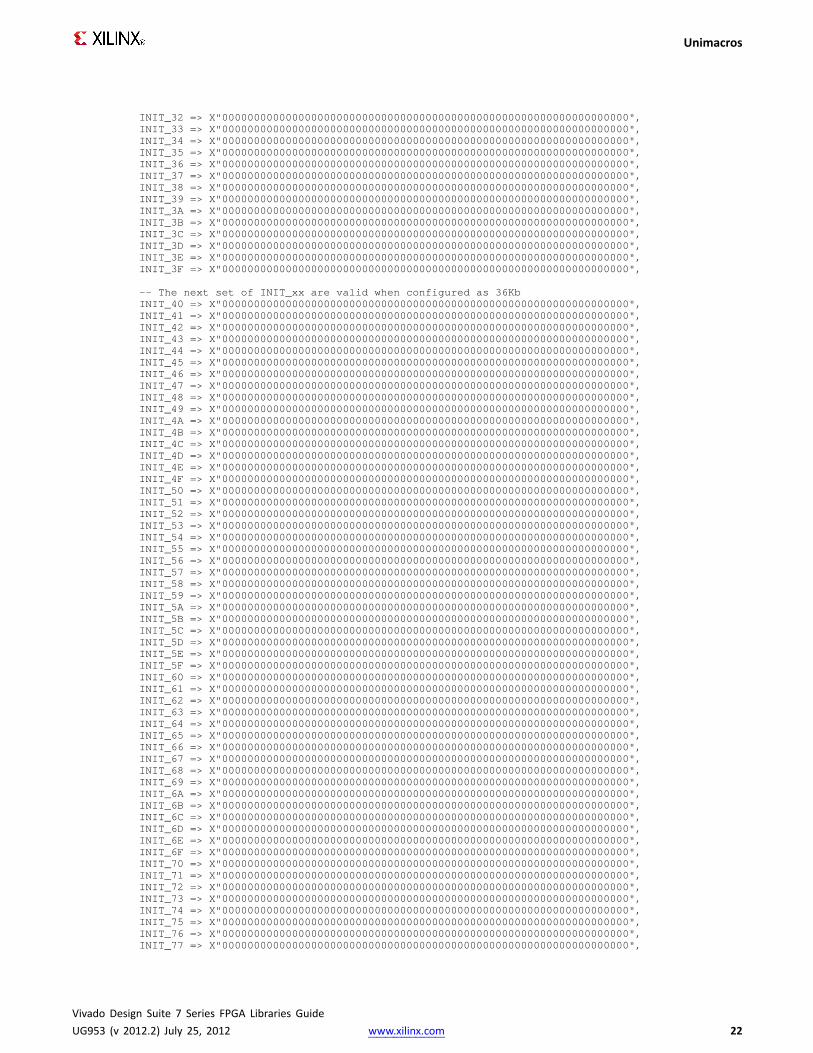
-- The next set of INIT_xx are valid when configured as 36KbINIT_40 => X"0000000000000000000000000000000000000000000000000000000000000000",INIT_41 => X"0000000000000000000000000000000000000000000000000000000000000000",INIT_42 => X"0000000000000000000000000000000000000000000000000000000000000000",INIT_43 => X"0000000000000000000000000000000000000000000000000000000000000000",INIT_44 => X"0000000000000000000000000000000000000000000000000000000000000000",INIT_45 => X"0000000000000000000000000000000000000000000000000000000000000000",INIT_46 => X"0000000000000000000000000000000000000000000000000000000000000000",INIT_47 => X"0000000000000000000000000000000000000000000000000000000000000000",INIT_48 => X"0000000000000000000000000000000000000000000000000000000000000000",INIT_49 => X"0000000000000000000000000000000000000000000000000000000000000000",INIT_4A => X"0000000000000000000000000000000000000000000000000000000000000000",INIT_4B => X"0000000000000000000000000000000000000000000000000000000000000000",INIT_4C => X"0000000000000000000000000000000000000000000000000000000000000000",INIT_4D => X"0000000000000000000000000000000000000000000000000000000000000000",INIT_4E => X"0000000000000000000000000000000000000000000000000000000000000000",INIT_4F => X"0000000000000000000000000000000000000000000000000000000000000000",INIT_50 => X"0000000000000000000000000000000000000000000000000000000000000000",INIT_51 => X"0000000000000000000000000000000000000000000000000000000000000000",INIT_52 => X"0000000000000000000000000000000000000000000000000000000000000000",INIT_53 => X"0000000000000000000000000000000000000000000000000000000000000000",INIT_54 => X"0000000000000000000000000000000000000000000000000000000000000000",INIT_55 => X"0000000000000000000000000000000000000000000000000000000000000000",INIT_56 => X"0000000000000000000000000000000000000000000000000000000000000000",INIT_57 => X"0000000000000000000000000000000000000000000000000000000000000000",INIT_58 => X"0000000000000000000000000000000000000000000000000000000000000000",INIT_59 => X"0000000000000000000000000000000000000000000000000000000000000000",INIT_5A => X"0000000000000000000000000000000000000000000000000000000000000000",INIT_5B => X"0000000000000000000000000000000000000000000000000000000000000000",INIT_5C => X"0000000000000000000000000000000000000000000000000000000000000000",INIT_5D => X"0000000000000000000000000000000000000000000000000000000000000000",INIT_5E => X"0000000000000000000000000000000000000000000000000000000000000000",INIT_5F => X"0000000000000000000000000000000000000000000000000000000000000000",INIT_60 => X"0000000000000000000000000000000000000000000000000000000000000000",INIT_61 => X"0000000000000000000000000000000000000000000000000000000000000000",INIT_62 => X"0000000000000000000000000000000000000000000000000000000000000000",INIT_63 => X"0000000000000000000000000000000000000000000000000000000000000000",INIT_64 => X"0000000000000000000000000000000000000000000000000000000000000000",INIT_65 => X"0000000000000000000000000000000000000000000000000000000000000000",INIT_66 => X"0000000000000000000000000000000000000000000000000000000000000000",
Vivado Design Suite 7 Series FPGA Libraries GuideUG953 (v 2012.2) July 25, 2012 www.xilinx.com 11
Unimacros
INIT_67 => X"0000000000000000000000000000000000000000000000000000000000000000",INIT_68 => X"0000000000000000000000000000000000000000000000000000000000000000",INIT_69 => X"0000000000000000000000000000000000000000000000000000000000000000",INIT_6A => X"0000000000000000000000000000000000000000000000000000000000000000",INIT_6B => X"0000000000000000000000000000000000000000000000000000000000000000",INIT_6C => X"0000000000000000000000000000000000000000000000000000000000000000",INIT_6D => X"0000000000000000000000000000000000000000000000000000000000000000",INIT_6E => X"0000000000000000000000000000000000000000000000000000000000000000",INIT_6F => X"0000000000000000000000000000000000000000000000000000000000000000",INIT_70 => X"0000000000000000000000000000000000000000000000000000000000000000",INIT_71 => X"0000000000000000000000000000000000000000000000000000000000000000",INIT_72 => X"0000000000000000000000000000000000000000000000000000000000000000",INIT_73 => X"0000000000000000000000000000000000000000000000000000000000000000",INIT_74 => X"0000000000000000000000000000000000000000000000000000000000000000",INIT_75 => X"0000000000000000000000000000000000000000000000000000000000000000",INIT_76 => X"0000000000000000000000000000000000000000000000000000000000000000",INIT_77 => X"0000000000000000000000000000000000000000000000000000000000000000",INIT_78 => X"0000000000000000000000000000000000000000000000000000000000000000",INIT_79 => X"0000000000000000000000000000000000000000000000000000000000000000",INIT_7A => X"0000000000000000000000000000000000000000000000000000000000000000",INIT_7B => X"0000000000000000000000000000000000000000000000000000000000000000",INIT_7C => X"0000000000000000000000000000000000000000000000000000000000000000",INIT_7D => X"0000000000000000000000000000000000000000000000000000000000000000",INIT_7E => X"0000000000000000000000000000000000000000000000000000000000000000",INIT_7F => X"0000000000000000000000000000000000000000000000000000000000000000",
-- The next set of INITP_xx are for the parity bitsINITP_00 => X"0000000000000000000000000000000000000000000000000000000000000000",INITP_01 => X"0000000000000000000000000000000000000000000000000000000000000000",INITP_02 => X"0000000000000000000000000000000000000000000000000000000000000000",INITP_03 => X"0000000000000000000000000000000000000000000000000000000000000000",INITP_04 => X"0000000000000000000000000000000000000000000000000000000000000000",INITP_05 => X"0000000000000000000000000000000000000000000000000000000000000000",INITP_06 => X"0000000000000000000000000000000000000000000000000000000000000000",INITP_07 => X"0000000000000000000000000000000000000000000000000000000000000000",
-- The next set of INIT_xx are valid when configured as 36KbINITP_08 => X"0000000000000000000000000000000000000000000000000000000000000000",INITP_09 => X"0000000000000000000000000000000000000000000000000000000000000000",INITP_0A => X"0000000000000000000000000000000000000000000000000000000000000000",INITP_0B => X"0000000000000000000000000000000000000000000000000000000000000000",INITP_0C => X"0000000000000000000000000000000000000000000000000000000000000000",INITP_0D => X"0000000000000000000000000000000000000000000000000000000000000000",INITP_0E => X"0000000000000000000000000000000000000000000000000000000000000000",
port map (DO => DO, -- Output read data port, width defined by READ_WIDTHparameterDI => DI, -- Input write data port, width defined by WRITE_WIDTHparameterRDADDR=> RDADDR, -- Input read address, width defined by read port depthRDCLK => RDCLK, -- 1-bit input read clockRDEN=> RDEN, -- 1-bit input read port enableREGCE=> REGCE, -- 1-bit input read output register enableRST => RST, -- 1-bit input resetWE => WE, -- Input write enable, width defined by write port depthWRADDR=> WRADDR,-- Input write address, width defined by write port depthWRCLK=> WRCLK, -- 1-bit input write clockWREN=> WREN -- 1-bit input write port enable
);-- End of BRAM_SDP_MACRO_inst instantiation
Verilog Instantiation Template
// BRAM_SDP_MACRO:Simple Dual Port RAM// 7 Series// Xilinx HDL Libraries Guide, version 2012.2
///////////////////////////////////////////////////////////////////////// READ_WIDTH| BRAM_SIZE | READ Depth | RDADDRWidth | //// WRITE_WIDTH | | WRITE Depth | WRADDRWidth | WEWidth //// ============|===========|=============|==============|============//// 37-72 | "36Kb" | 512 | 9-bit | 8-bit //
Vivado Design Suite 7 Series FPGA Libraries GuideUG953 (v 2012.2) July 25, 2012 www.xilinx.com 12
Unimacros
// 19-36 | "36Kb" | 1024 | 10-bit | 4-bit //// 19-36 | "18Kb" | 512 | 9-bit | 4-bit //// 10-18 | "36Kb" | 2048 | 11-bit | 2-bit //// 10-18 | "18Kb" | 1024 | 10-bit | 2-bit //// 5-9 | "36Kb" | 4096 | 12-bit | 1-bit //// 5-9 | "18Kb" | 2048 | 11-bit | 1-bit //// 3-4 | "36Kb" | 8192 | 13-bit | 1-bit //// 3-4 | "18Kb" | 4096 | 12-bit | 1-bit //// 2 | "36Kb" | 16384 | 14-bit | 1-bit //// 2 | "18Kb" | 8192 | 13-bit | 1-bit //// 1 | "36Kb" | 32768 | 15-bit | 1-bit //// 1 | "18Kb" | 16384 | 14-bit | 1-bit /////////////////////////////////////////////////////////////////////////
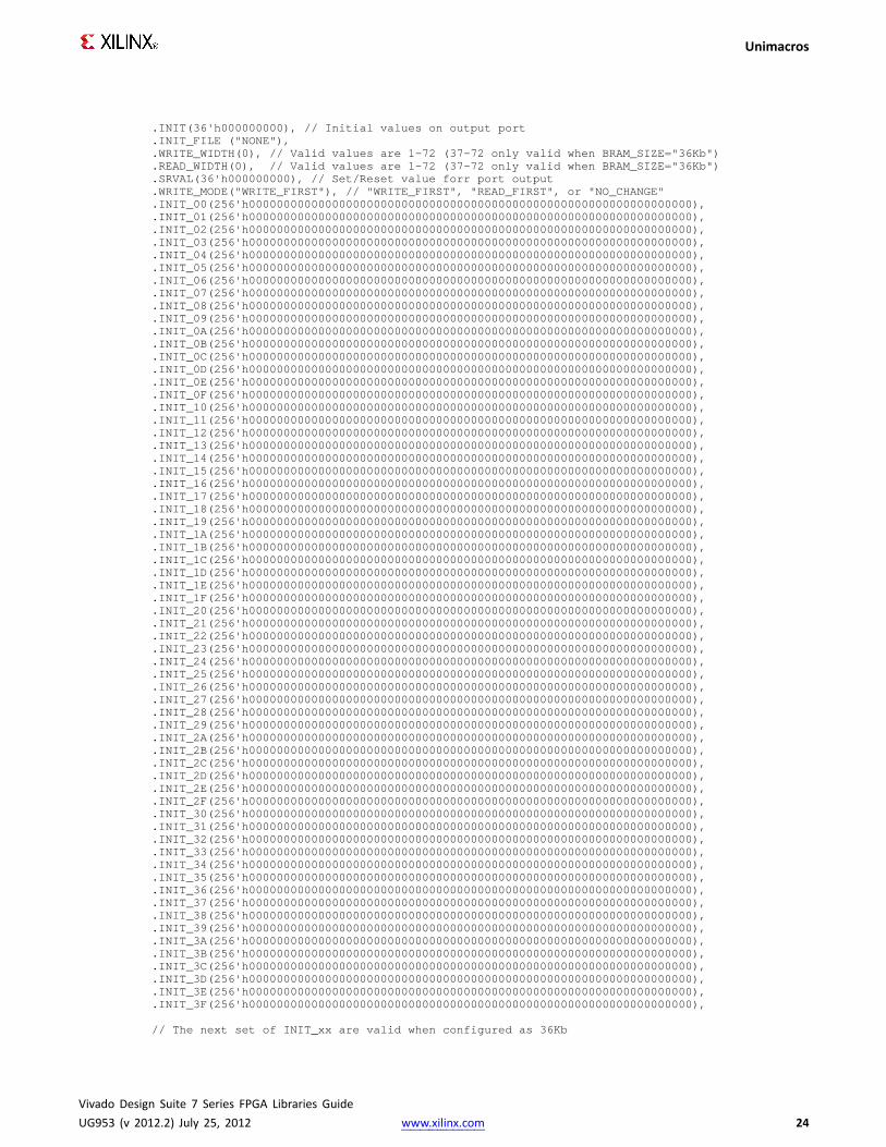
BRAM_SDP_MACRO#(.BRAM_SIZE("18Kb"), // Target BRAM, "18Kb" or "36Kb".DEVICE("7SERIES"), // Target device: "7SERIES".WRITE_WIDTH(0), // Valid values are 1-72 (37-72 only valid when BRAM_SIZE="36Kb").READ_WIDTH(0), // Valid values are 1-72 (37-72 only valid when BRAM_SIZE="36Kb").DO_REG(0), // Optional output register (0 or 1).INIT_FILE ("NONE"),.SIM_COLLISION_CHECK ("ALL"), // Collision check enable "ALL", "WARNING_ONLY",
// "GENERATE_X_ONLY"or "NONE".SRVAL(72'h000000000000000000), // Set/Reset value forr port output.INIT(72'h000000000000000000), // Initial values on output port.WRITE_MODE("WRITE_FIRST"), // Specify "READ_FIRST" forr same clock or synchronous clocks
// Specify "WRITE_FIRST forr asynchronous clocks on ports.INIT_00(256'h0000000000000000000000000000000000000000000000000000000000000000),.INIT_01(256'h0000000000000000000000000000000000000000000000000000000000000000),.INIT_02(256'h0000000000000000000000000000000000000000000000000000000000000000),.INIT_03(256'h0000000000000000000000000000000000000000000000000000000000000000),.INIT_04(256'h0000000000000000000000000000000000000000000000000000000000000000),.INIT_05(256'h0000000000000000000000000000000000000000000000000000000000000000),.INIT_06(256'h0000000000000000000000000000000000000000000000000000000000000000),.INIT_07(256'h0000000000000000000000000000000000000000000000000000000000000000),.INIT_08(256'h0000000000000000000000000000000000000000000000000000000000000000),.INIT_09(256'h0000000000000000000000000000000000000000000000000000000000000000),.INIT_0A(256'h0000000000000000000000000000000000000000000000000000000000000000),.INIT_0B(256'h0000000000000000000000000000000000000000000000000000000000000000),.INIT_0C(256'h0000000000000000000000000000000000000000000000000000000000000000),.INIT_0D(256'h0000000000000000000000000000000000000000000000000000000000000000),.INIT_0E(256'h0000000000000000000000000000000000000000000000000000000000000000),.INIT_0F(256'h0000000000000000000000000000000000000000000000000000000000000000),.INIT_10(256'h0000000000000000000000000000000000000000000000000000000000000000),.INIT_11(256'h0000000000000000000000000000000000000000000000000000000000000000),.INIT_12(256'h0000000000000000000000000000000000000000000000000000000000000000),.INIT_13(256'h0000000000000000000000000000000000000000000000000000000000000000),.INIT_14(256'h0000000000000000000000000000000000000000000000000000000000000000),.INIT_15(256'h0000000000000000000000000000000000000000000000000000000000000000),.INIT_16(256'h0000000000000000000000000000000000000000000000000000000000000000),.INIT_17(256'h0000000000000000000000000000000000000000000000000000000000000000),.INIT_18(256'h0000000000000000000000000000000000000000000000000000000000000000),.INIT_19(256'h0000000000000000000000000000000000000000000000000000000000000000),.INIT_1A(256'h0000000000000000000000000000000000000000000000000000000000000000),.INIT_1B(256'h0000000000000000000000000000000000000000000000000000000000000000),.INIT_1C(256'h0000000000000000000000000000000000000000000000000000000000000000),.INIT_1D(256'h0000000000000000000000000000000000000000000000000000000000000000),.INIT_1E(256'h0000000000000000000000000000000000000000000000000000000000000000),.INIT_1F(256'h0000000000000000000000000000000000000000000000000000000000000000),.INIT_20(256'h0000000000000000000000000000000000000000000000000000000000000000),.INIT_21(256'h0000000000000000000000000000000000000000000000000000000000000000),.INIT_22(256'h0000000000000000000000000000000000000000000000000000000000000000),.INIT_23(256'h0000000000000000000000000000000000000000000000000000000000000000),.INIT_24(256'h0000000000000000000000000000000000000000000000000000000000000000),.INIT_25(256'h0000000000000000000000000000000000000000000000000000000000000000),.INIT_26(256'h0000000000000000000000000000000000000000000000000000000000000000),.INIT_27(256'h0000000000000000000000000000000000000000000000000000000000000000),.INIT_28(256'h0000000000000000000000000000000000000000000000000000000000000000),.INIT_29(256'h0000000000000000000000000000000000000000000000000000000000000000),.INIT_2A(256'h0000000000000000000000000000000000000000000000000000000000000000),.INIT_2B(256'h0000000000000000000000000000000000000000000000000000000000000000),.INIT_2C(256'h0000000000000000000000000000000000000000000000000000000000000000),
Vivado Design Suite 7 Series FPGA Libraries GuideUG953 (v 2012.2) July 25, 2012 www.xilinx.com 13

Unimacros
.INIT_2D(256'h0000000000000000000000000000000000000000000000000000000000000000),
.INIT_2E(256'h0000000000000000000000000000000000000000000000000000000000000000),
.INIT_2F(256'h0000000000000000000000000000000000000000000000000000000000000000),
.INIT_30(256'h0000000000000000000000000000000000000000000000000000000000000000),
.INIT_31(256'h0000000000000000000000000000000000000000000000000000000000000000),
.INIT_32(256'h0000000000000000000000000000000000000000000000000000000000000000),
.INIT_33(256'h0000000000000000000000000000000000000000000000000000000000000000),
.INIT_34(256'h0000000000000000000000000000000000000000000000000000000000000000),
.INIT_35(256'h0000000000000000000000000000000000000000000000000000000000000000),
.INIT_36(256'h0000000000000000000000000000000000000000000000000000000000000000),
.INIT_37(256'h0000000000000000000000000000000000000000000000000000000000000000),
.INIT_38(256'h0000000000000000000000000000000000000000000000000000000000000000),
.INIT_39(256'h0000000000000000000000000000000000000000000000000000000000000000),
.INIT_3A(256'h0000000000000000000000000000000000000000000000000000000000000000),
.INIT_3B(256'h0000000000000000000000000000000000000000000000000000000000000000),
.INIT_3C(256'h0000000000000000000000000000000000000000000000000000000000000000),
.INIT_3D(256'h0000000000000000000000000000000000000000000000000000000000000000),
.INIT_3E(256'h0000000000000000000000000000000000000000000000000000000000000000),
.INIT_3F(256'h0000000000000000000000000000000000000000000000000000000000000000),
// The next set of INIT_xx are valid when configured as 36Kb.INIT_40(256'h0000000000000000000000000000000000000000000000000000000000000000),.INIT_41(256'h0000000000000000000000000000000000000000000000000000000000000000),.INIT_42(256'h0000000000000000000000000000000000000000000000000000000000000000),.INIT_43(256'h0000000000000000000000000000000000000000000000000000000000000000),.INIT_44(256'h0000000000000000000000000000000000000000000000000000000000000000),.INIT_45(256'h0000000000000000000000000000000000000000000000000000000000000000),.INIT_46(256'h0000000000000000000000000000000000000000000000000000000000000000),.INIT_47(256'h0000000000000000000000000000000000000000000000000000000000000000),.INIT_48(256'h0000000000000000000000000000000000000000000000000000000000000000),.INIT_49(256'h0000000000000000000000000000000000000000000000000000000000000000),.INIT_4A(256'h0000000000000000000000000000000000000000000000000000000000000000),.INIT_4B(256'h0000000000000000000000000000000000000000000000000000000000000000),.INIT_4C(256'h0000000000000000000000000000000000000000000000000000000000000000),.INIT_4D(256'h0000000000000000000000000000000000000000000000000000000000000000),.INIT_4E(256'h0000000000000000000000000000000000000000000000000000000000000000),.INIT_4F(256'h0000000000000000000000000000000000000000000000000000000000000000),.INIT_50(256'h0000000000000000000000000000000000000000000000000000000000000000),.INIT_51(256'h0000000000000000000000000000000000000000000000000000000000000000),.INIT_52(256'h0000000000000000000000000000000000000000000000000000000000000000),.INIT_53(256'h0000000000000000000000000000000000000000000000000000000000000000),.INIT_54(256'h0000000000000000000000000000000000000000000000000000000000000000),.INIT_55(256'h0000000000000000000000000000000000000000000000000000000000000000),.INIT_56(256'h0000000000000000000000000000000000000000000000000000000000000000),.INIT_57(256'h0000000000000000000000000000000000000000000000000000000000000000),.INIT_58(256'h0000000000000000000000000000000000000000000000000000000000000000),.INIT_59(256'h0000000000000000000000000000000000000000000000000000000000000000),.INIT_5A(256'h0000000000000000000000000000000000000000000000000000000000000000),.INIT_5B(256'h0000000000000000000000000000000000000000000000000000000000000000),.INIT_5C(256'h0000000000000000000000000000000000000000000000000000000000000000),.INIT_5D(256'h0000000000000000000000000000000000000000000000000000000000000000),.INIT_5E(256'h0000000000000000000000000000000000000000000000000000000000000000),.INIT_5F(256'h0000000000000000000000000000000000000000000000000000000000000000),.INIT_60(256'h0000000000000000000000000000000000000000000000000000000000000000),.INIT_61(256'h0000000000000000000000000000000000000000000000000000000000000000),.INIT_62(256'h0000000000000000000000000000000000000000000000000000000000000000),.INIT_63(256'h0000000000000000000000000000000000000000000000000000000000000000),.INIT_64(256'h0000000000000000000000000000000000000000000000000000000000000000),.INIT_65(256'h0000000000000000000000000000000000000000000000000000000000000000),.INIT_66(256'h0000000000000000000000000000000000000000000000000000000000000000),.INIT_67(256'h0000000000000000000000000000000000000000000000000000000000000000),.INIT_68(256'h0000000000000000000000000000000000000000000000000000000000000000),.INIT_69(256'h0000000000000000000000000000000000000000000000000000000000000000),.INIT_6A(256'h0000000000000000000000000000000000000000000000000000000000000000),.INIT_6B(256'h0000000000000000000000000000000000000000000000000000000000000000),.INIT_6C(256'h0000000000000000000000000000000000000000000000000000000000000000),.INIT_6D(256'h0000000000000000000000000000000000000000000000000000000000000000),.INIT_6E(256'h0000000000000000000000000000000000000000000000000000000000000000),.INIT_6F(256'h0000000000000000000000000000000000000000000000000000000000000000),.INIT_70(256'h0000000000000000000000000000000000000000000000000000000000000000),.INIT_71(256'h0000000000000000000000000000000000000000000000000000000000000000),.INIT_72(256'h0000000000000000000000000000000000000000000000000000000000000000),
Vivado Design Suite 7 Series FPGA Libraries GuideUG953 (v 2012.2) July 25, 2012 www.xilinx.com 14
Unimacros
.INIT_73(256'h0000000000000000000000000000000000000000000000000000000000000000),
.INIT_74(256'h0000000000000000000000000000000000000000000000000000000000000000),
.INIT_75(256'h0000000000000000000000000000000000000000000000000000000000000000),
.INIT_76(256'h0000000000000000000000000000000000000000000000000000000000000000),
.INIT_77(256'h0000000000000000000000000000000000000000000000000000000000000000),
.INIT_78(256'h0000000000000000000000000000000000000000000000000000000000000000),
.INIT_79(256'h0000000000000000000000000000000000000000000000000000000000000000),
.INIT_7A(256'h0000000000000000000000000000000000000000000000000000000000000000),
.INIT_7B(256'h0000000000000000000000000000000000000000000000000000000000000000),
.INIT_7C(256'h0000000000000000000000000000000000000000000000000000000000000000),
.INIT_7D(256'h0000000000000000000000000000000000000000000000000000000000000000),
.INIT_7E(256'h0000000000000000000000000000000000000000000000000000000000000000),
.INIT_7F(256'h0000000000000000000000000000000000000000000000000000000000000000),
// The next set of INITP_xx are forr the parity bits.INITP_00(256'h0000000000000000000000000000000000000000000000000000000000000000),.INITP_01(256'h0000000000000000000000000000000000000000000000000000000000000000),.INITP_02(256'h0000000000000000000000000000000000000000000000000000000000000000),.INITP_03(256'h0000000000000000000000000000000000000000000000000000000000000000),.INITP_04(256'h0000000000000000000000000000000000000000000000000000000000000000),.INITP_05(256'h0000000000000000000000000000000000000000000000000000000000000000),.INITP_06(256'h0000000000000000000000000000000000000000000000000000000000000000),.INITP_07(256'h0000000000000000000000000000000000000000000000000000000000000000),
// The next set of INITP_xx are valid when configured as 36Kb.INITP_08(256'h0000000000000000000000000000000000000000000000000000000000000000),.INITP_09(256'h0000000000000000000000000000000000000000000000000000000000000000),.INITP_0A(256'h0000000000000000000000000000000000000000000000000000000000000000),.INITP_0B(256'h0000000000000000000000000000000000000000000000000000000000000000),.INITP_0C(256'h0000000000000000000000000000000000000000000000000000000000000000),.INITP_0D(256'h0000000000000000000000000000000000000000000000000000000000000000),.INITP_0E(256'h0000000000000000000000000000000000000000000000000000000000000000),.INITP_0F(256'h0000000000000000000000000000000000000000000000000000000000000000)
) BRAM_SDP_MACRO_inst(.DO(DO), // Output read data port, width defined by READ_WIDTHparameter.DI(DI), // Input write data port, width defined by WRITE_WIDTHparameter.RDADDR(RDADDR), // Input read address, width defined by read port depth.RDCLK(RDCLK), // 1-bit input read clock.RDEN(RDEN), // 1-bit input read port enable.REGCE(REGCE), // 1-bit input read output register enable.RST(RST), // 1-bit input reset.WE(WE), // Input write enable, width defined by write port depth.WRADDR(WRADDR),// Input write address, width defined by write port depth.WRCLK(WRCLK), // 1-bit input write clock.WREN(WREN) // 1-bit input write port enable
);
// End of BRAM_SDP_MACRO_inst instantiation
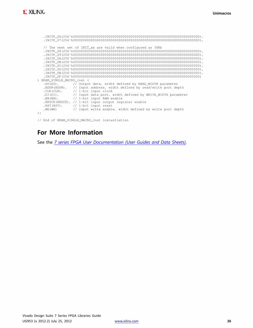
For More InformationSee the 7 series FPGA User Documentation (User Guides and Data Sheets).
Vivado Design Suite 7 Series FPGA Libraries GuideUG953 (v 2012.2) July 25, 2012 www.xilinx.com 15

Unimacros
BRAM_SINGLE_MACROMacro: Single Port RAM
Introduction7 series FPGA devices contain several block RAM memories that can be configured asgeneral-purpose 36Kb or 18Kb RAM/ROM memories. These single-port, block RAM memoriesoffer fast and flexible storage of large amounts of on-chip data. Byte-enable write operationsare possible, and an optional output register can be used to reduce the clock-to-out times ofthe RAM.
Port DescriptionName Direction Width Function
DO Output See Configuration Tablebelow.
Data output bus addressed by ADDR.
DI Input See Configuration Tablebelow.
Data input bus addressed by ADDR.
ADDR Input See Configuration Tablebelow.
Address input bus.
WE Input See Configuration Tablebelow.
Byte-Wide Write enable.
EN Input 1 Write/Read enables.
RST Input 1 Output registers synchronous reset.
Vivado Design Suite 7 Series FPGA Libraries GuideUG953 (v 2012.2) July 25, 2012 www.xilinx.com 16

Unimacros
Name Direction Width Function
REGCE Input 1 Output register clock enable input (valid onlywhen DO_REG=1).
CLK Input 1 Clock input.
Port ConfigurationThis unimacro is a parameterizable version of the primitive, and can be instantiated only. Usethis table to correctly configure the unimacro to meet design needs.
WRITE_WIDTH READ_WIDTH BRAM_SIZE ADDR WE
72 - 37 9
36 - 19 10
18 - 10 11
9 - 5 12
4 - 3 13
2 14
72 - 37
1
36Kb
15
8
36 - 19 10
18-10 11
9 - 5 12
4 - 3 13
2 14
36 - 19
1
36Kb
15
4
36 - 19 11
18-10 11
9 - 5 12
4 - 3 13
2 14
18 - 10
1
36Kb
15
2
36-19 12
18-10 12
9 - 5 12
4 - 3 13
2 14
9 - 5
1
36Kb
15
1
Vivado Design Suite 7 Series FPGA Libraries GuideUG953 (v 2012.2) July 25, 2012 www.xilinx.com 17

Unimacros
WRITE_WIDTH READ_WIDTH BRAM_SIZE ADDR WE
36-19 13
18-10 13
9 - 5 13
4 - 3 13
2 14
4 - 3
1
36Kb
15
1
36-19 14
18-10 14
9 - 5 14
4 - 3 14
2 14
2
1
36Kb
15
1
36 - 19 15
18 - 10 15
9 - 5 15
3 - 4 15
2 15
1
1
36Kb
15
1
18-10 10
9 - 5 11
4 - 3 12
2 13
18-10
1
18Kb
14
2
18-10 11
9 - 5 11
4 - 3 12
2 13
9 - 5
1
18Kb
14
1
Vivado Design Suite 7 Series FPGA Libraries GuideUG953 (v 2012.2) July 25, 2012 www.xilinx.com 18

Unimacros
WRITE_WIDTH READ_WIDTH BRAM_SIZE ADDR WE
18-10 12
9 - 5 12
4 - 3 12
2 13
4 - 3
1
18Kb
14
1
18-10 13
9 - 5 13
4 - 3 13
2 13
2
1
18Kb
14
1
18-10 14
9 - 5 14
4 - 3 14
2 14
1
1
18Kb
14
1
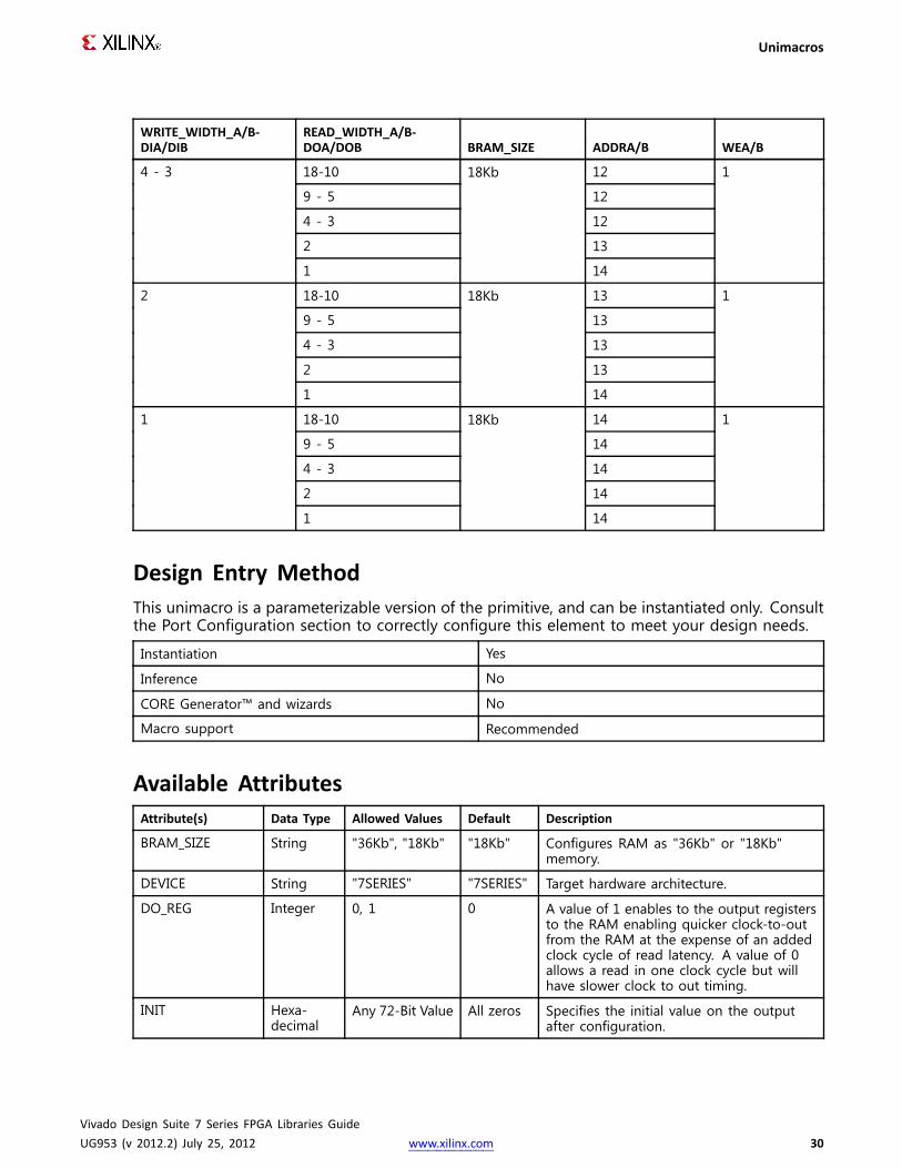
Design Entry MethodThis unimacro is a parameterizable version of the primitive, and can be instantiated only. Consultthe Port Configuration section to correctly configure this element to meet your design needs.
Instantiation Yes
Inference No
CORE Generator™ and wizards No
Macro support Recommended
Available AttributesAttribute Data Type Allowed Values Default Description
BRAM_SIZE String "36Kb", "18Kb" "18Kb" Configures RAM as "36Kb" or "18Kb"memory.
DEVICE String "7SERIES" "7SERIES" Target hardware architecture.
DO_REG Integer 0, 1 0 A value of 1 enables to the outputregisters to the RAM enabling quickerclock-to-out from the RAM at theexpense of an added clock cycle ofread latency. A value of 0 allows a readin one clock cycle but will have slowerclock to out timing.
Vivado Design Suite 7 Series FPGA Libraries GuideUG953 (v 2012.2) July 25, 2012 www.xilinx.com 19

Unimacros
Attribute Data Type Allowed Values Default Description
READ_WIDTH,WRITE_WIDTH
Integer 1 - 36 1 Specifies the size of the DI and DObuses.
The following combinations areallowed:
• READ_WIDTH = WRITE_WIDTH
• If asymmetric, READ_WIDTHand WRITE_WIDTH must bein the ratio of 2, or must bevalues allowed by the unisim(1, 2, 4, 8, 9, 16, 18, 32, 36, 64,72)
INIT_FILE String Stringrepresentingfile name andlocation.
None Name of the file containing initialvalues.
WRITE_MODE String "READ_FIRST","WRITE_FIRST","NO_CHANGE"
"WRITE_FIRST" Specifies write mode to the memory.
INIT Hexadecimal Any 72-Bit Value All zeros Specifies the initial value on the outputafter configuration.
SRVAL Hexadecimal Any 72-Bit Value All zeroes Specifies the output value of on theDO port upon the assertion of thesynchronous reset (RST) signal.
INIT_00 toINIT_FF
Hexadecimal Any 256-BitValue
All zeroes Allows specification of the initialcontents of the 16Kb or 32Kb datamemory array.
INITP_00 toINITP_0F
Hexadecimal Any 256-BitValue
All zeroes Allows specification of the initialcontents of the 2Kb or 4Kb parity datamemory array.
VHDL Instantiation TemplateUnless they already exist, copy the following two statements and paste them before the entitydeclaration.Library UNISIM;use UNISIM.vcomponents.all;
-- BRAM_SINGLE_MACRO:Single Port RAM-- 7 Series-- Xilinx HDL Libraries Guide, version 2012.2
-- Note - This Unimacro model assumes the port directions to be "downto".-- Simulation of this model with "to" in the port directions could lead to erroneous results.
----------------------------------------------------------------------- READ_WIDTH| BRAM_SIZE | READ Depth | ADDRWidth | ---- WRITE_WIDTH | | WRITE Depth | | WEWidth ---- ============|===========|=============|============|============---- 37-72 | "36Kb" | 512 | 9-bit | 8-bit ---- 19-36 | "36Kb" | 1024 | 10-bit | 4-bit ---- 19-36 | "18Kb" | 512 | 9-bit | 4-bit ---- 10-18 | "36Kb" | 2048 | 11-bit | 2-bit ---- 10-18 | "18Kb" | 1024 | 10-bit | 2-bit --
Vivado Design Suite 7 Series FPGA Libraries GuideUG953 (v 2012.2) July 25, 2012 www.xilinx.com 20
Unimacros
-- 5-9 | "36Kb" | 4096 | 12-bit | 1-bit ---- 5-9 | "18Kb" | 2048 | 11-bit | 1-bit ---- 3-4 | "36Kb" | 8192 | 13-bit | 1-bit ---- 3-4 | "18Kb" | 4096 | 12-bit | 1-bit ---- 2 | "36Kb" | 16384 | 14-bit | 1-bit ---- 2 | "18Kb" | 8192 | 13-bit | 1-bit ---- 1 | "36Kb" | 32768 | 15-bit | 1-bit ---- 1 | "18Kb" | 16384 | 14-bit | 1-bit -----------------------------------------------------------------------
BRAM_SINGLE_MACRO_inst : BRAM_SINGLE_MACROgeneric map (
BRAM_SIZE => "18Kb", -- Target BRAM, "18Kb" or "36Kb"DEVICE => "7SERIES", -- Target Device: "VIRTEX5", "7SERIES", "VIRTEX6, "SPARTAN6"DO_REG=> 0, -- Optional output register (0 or 1)INIT => X"000000000", -- Initial values on output portINIT_FILE => "NONE",WRITE_WIDTH=> 0, -- Valid values are 1-72 (37-72 only valid when BRAM_SIZE="36Kb")READ_WIDTH=> 0, -- Valid values are 1-72 (37-72 only valid when BRAM_SIZE="36Kb")SRVAL => X"000000000", -- Set/Reset value for port outputWRITE_MODE=> "WRITE_FIRST", -- "WRITE_FIRST", "READ_FIRST" or "NO_CHANGE"-- The following INIT_xx declarations specify the initial contents of the RAMINIT_00 => X"0000000000000000000000000000000000000000000000000000000000000000",INIT_01 => X"0000000000000000000000000000000000000000000000000000000000000000",INIT_02 => X"0000000000000000000000000000000000000000000000000000000000000000",INIT_03 => X"0000000000000000000000000000000000000000000000000000000000000000",INIT_04 => X"0000000000000000000000000000000000000000000000000000000000000000",INIT_05 => X"0000000000000000000000000000000000000000000000000000000000000000",INIT_06 => X"0000000000000000000000000000000000000000000000000000000000000000",INIT_07 => X"0000000000000000000000000000000000000000000000000000000000000000",INIT_08 => X"0000000000000000000000000000000000000000000000000000000000000000",INIT_09 => X"0000000000000000000000000000000000000000000000000000000000000000",INIT_0A => X"0000000000000000000000000000000000000000000000000000000000000000",INIT_0B => X"0000000000000000000000000000000000000000000000000000000000000000",INIT_0C => X"0000000000000000000000000000000000000000000000000000000000000000",INIT_0D => X"0000000000000000000000000000000000000000000000000000000000000000",INIT_0E => X"0000000000000000000000000000000000000000000000000000000000000000",INIT_0F => X"0000000000000000000000000000000000000000000000000000000000000000",INIT_10 => X"0000000000000000000000000000000000000000000000000000000000000000",INIT_11 => X"0000000000000000000000000000000000000000000000000000000000000000",INIT_12 => X"0000000000000000000000000000000000000000000000000000000000000000",INIT_13 => X"0000000000000000000000000000000000000000000000000000000000000000",INIT_14 => X"0000000000000000000000000000000000000000000000000000000000000000",INIT_15 => X"0000000000000000000000000000000000000000000000000000000000000000",INIT_16 => X"0000000000000000000000000000000000000000000000000000000000000000",INIT_17 => X"0000000000000000000000000000000000000000000000000000000000000000",INIT_18 => X"0000000000000000000000000000000000000000000000000000000000000000",INIT_19 => X"0000000000000000000000000000000000000000000000000000000000000000",INIT_1A => X"0000000000000000000000000000000000000000000000000000000000000000",INIT_1B => X"0000000000000000000000000000000000000000000000000000000000000000",INIT_1C => X"0000000000000000000000000000000000000000000000000000000000000000",INIT_1D => X"0000000000000000000000000000000000000000000000000000000000000000",INIT_1E => X"0000000000000000000000000000000000000000000000000000000000000000",INIT_1F => X"0000000000000000000000000000000000000000000000000000000000000000",INIT_20 => X"0000000000000000000000000000000000000000000000000000000000000000",INIT_21 => X"0000000000000000000000000000000000000000000000000000000000000000",INIT_22 => X"0000000000000000000000000000000000000000000000000000000000000000",INIT_23 => X"0000000000000000000000000000000000000000000000000000000000000000",INIT_24 => X"0000000000000000000000000000000000000000000000000000000000000000",INIT_25 => X"0000000000000000000000000000000000000000000000000000000000000000",INIT_26 => X"0000000000000000000000000000000000000000000000000000000000000000",INIT_27 => X"0000000000000000000000000000000000000000000000000000000000000000",INIT_28 => X"0000000000000000000000000000000000000000000000000000000000000000",INIT_29 => X"0000000000000000000000000000000000000000000000000000000000000000",INIT_2A => X"0000000000000000000000000000000000000000000000000000000000000000",INIT_2B => X"0000000000000000000000000000000000000000000000000000000000000000",INIT_2C => X"0000000000000000000000000000000000000000000000000000000000000000",INIT_2D => X"0000000000000000000000000000000000000000000000000000000000000000",INIT_2E => X"0000000000000000000000000000000000000000000000000000000000000000",INIT_2F => X"0000000000000000000000000000000000000000000000000000000000000000",INIT_30 => X"0000000000000000000000000000000000000000000000000000000000000000",INIT_31 => X"0000000000000000000000000000000000000000000000000000000000000000",
Vivado Design Suite 7 Series FPGA Libraries GuideUG953 (v 2012.2) July 25, 2012 www.xilinx.com 21
Unimacros
INIT_32 => X"0000000000000000000000000000000000000000000000000000000000000000",INIT_33 => X"0000000000000000000000000000000000000000000000000000000000000000",INIT_34 => X"0000000000000000000000000000000000000000000000000000000000000000",INIT_35 => X"0000000000000000000000000000000000000000000000000000000000000000",INIT_36 => X"0000000000000000000000000000000000000000000000000000000000000000",INIT_37 => X"0000000000000000000000000000000000000000000000000000000000000000",INIT_38 => X"0000000000000000000000000000000000000000000000000000000000000000",INIT_39 => X"0000000000000000000000000000000000000000000000000000000000000000",INIT_3A => X"0000000000000000000000000000000000000000000000000000000000000000",INIT_3B => X"0000000000000000000000000000000000000000000000000000000000000000",INIT_3C => X"0000000000000000000000000000000000000000000000000000000000000000",INIT_3D => X"0000000000000000000000000000000000000000000000000000000000000000",INIT_3E => X"0000000000000000000000000000000000000000000000000000000000000000",INIT_3F => X"0000000000000000000000000000000000000000000000000000000000000000",
-- The next set of INIT_xx are valid when configured as 36KbINIT_40 => X"0000000000000000000000000000000000000000000000000000000000000000",INIT_41 => X"0000000000000000000000000000000000000000000000000000000000000000",INIT_42 => X"0000000000000000000000000000000000000000000000000000000000000000",INIT_43 => X"0000000000000000000000000000000000000000000000000000000000000000",INIT_44 => X"0000000000000000000000000000000000000000000000000000000000000000",INIT_45 => X"0000000000000000000000000000000000000000000000000000000000000000",INIT_46 => X"0000000000000000000000000000000000000000000000000000000000000000",INIT_47 => X"0000000000000000000000000000000000000000000000000000000000000000",INIT_48 => X"0000000000000000000000000000000000000000000000000000000000000000",INIT_49 => X"0000000000000000000000000000000000000000000000000000000000000000",INIT_4A => X"0000000000000000000000000000000000000000000000000000000000000000",INIT_4B => X"0000000000000000000000000000000000000000000000000000000000000000",INIT_4C => X"0000000000000000000000000000000000000000000000000000000000000000",INIT_4D => X"0000000000000000000000000000000000000000000000000000000000000000",INIT_4E => X"0000000000000000000000000000000000000000000000000000000000000000",INIT_4F => X"0000000000000000000000000000000000000000000000000000000000000000",INIT_50 => X"0000000000000000000000000000000000000000000000000000000000000000",INIT_51 => X"0000000000000000000000000000000000000000000000000000000000000000",INIT_52 => X"0000000000000000000000000000000000000000000000000000000000000000",INIT_53 => X"0000000000000000000000000000000000000000000000000000000000000000",INIT_54 => X"0000000000000000000000000000000000000000000000000000000000000000",INIT_55 => X"0000000000000000000000000000000000000000000000000000000000000000",INIT_56 => X"0000000000000000000000000000000000000000000000000000000000000000",INIT_57 => X"0000000000000000000000000000000000000000000000000000000000000000",INIT_58 => X"0000000000000000000000000000000000000000000000000000000000000000",INIT_59 => X"0000000000000000000000000000000000000000000000000000000000000000",INIT_5A => X"0000000000000000000000000000000000000000000000000000000000000000",INIT_5B => X"0000000000000000000000000000000000000000000000000000000000000000",INIT_5C => X"0000000000000000000000000000000000000000000000000000000000000000",INIT_5D => X"0000000000000000000000000000000000000000000000000000000000000000",INIT_5E => X"0000000000000000000000000000000000000000000000000000000000000000",INIT_5F => X"0000000000000000000000000000000000000000000000000000000000000000",INIT_60 => X"0000000000000000000000000000000000000000000000000000000000000000",INIT_61 => X"0000000000000000000000000000000000000000000000000000000000000000",INIT_62 => X"0000000000000000000000000000000000000000000000000000000000000000",INIT_63 => X"0000000000000000000000000000000000000000000000000000000000000000",INIT_64 => X"0000000000000000000000000000000000000000000000000000000000000000",INIT_65 => X"0000000000000000000000000000000000000000000000000000000000000000",INIT_66 => X"0000000000000000000000000000000000000000000000000000000000000000",INIT_67 => X"0000000000000000000000000000000000000000000000000000000000000000",INIT_68 => X"0000000000000000000000000000000000000000000000000000000000000000",INIT_69 => X"0000000000000000000000000000000000000000000000000000000000000000",INIT_6A => X"0000000000000000000000000000000000000000000000000000000000000000",INIT_6B => X"0000000000000000000000000000000000000000000000000000000000000000",INIT_6C => X"0000000000000000000000000000000000000000000000000000000000000000",INIT_6D => X"0000000000000000000000000000000000000000000000000000000000000000",INIT_6E => X"0000000000000000000000000000000000000000000000000000000000000000",INIT_6F => X"0000000000000000000000000000000000000000000000000000000000000000",INIT_70 => X"0000000000000000000000000000000000000000000000000000000000000000",INIT_71 => X"0000000000000000000000000000000000000000000000000000000000000000",INIT_72 => X"0000000000000000000000000000000000000000000000000000000000000000",INIT_73 => X"0000000000000000000000000000000000000000000000000000000000000000",INIT_74 => X"0000000000000000000000000000000000000000000000000000000000000000",INIT_75 => X"0000000000000000000000000000000000000000000000000000000000000000",INIT_76 => X"0000000000000000000000000000000000000000000000000000000000000000",INIT_77 => X"0000000000000000000000000000000000000000000000000000000000000000",
Vivado Design Suite 7 Series FPGA Libraries GuideUG953 (v 2012.2) July 25, 2012 www.xilinx.com 22

Unimacros
INIT_78 => X"0000000000000000000000000000000000000000000000000000000000000000",INIT_79 => X"0000000000000000000000000000000000000000000000000000000000000000",INIT_7A => X"0000000000000000000000000000000000000000000000000000000000000000",INIT_7B => X"0000000000000000000000000000000000000000000000000000000000000000",INIT_7C => X"0000000000000000000000000000000000000000000000000000000000000000",INIT_7D => X"0000000000000000000000000000000000000000000000000000000000000000",INIT_7E => X"0000000000000000000000000000000000000000000000000000000000000000",INIT_7F => X"0000000000000000000000000000000000000000000000000000000000000000",
-- The next set of INITP_xx are for the parity bitsINITP_00 => X"0000000000000000000000000000000000000000000000000000000000000000",INITP_01 => X"0000000000000000000000000000000000000000000000000000000000000000",INITP_02 => X"0000000000000000000000000000000000000000000000000000000000000000",INITP_03 => X"0000000000000000000000000000000000000000000000000000000000000000",INITP_04 => X"0000000000000000000000000000000000000000000000000000000000000000",INITP_05 => X"0000000000000000000000000000000000000000000000000000000000000000",INITP_06 => X"0000000000000000000000000000000000000000000000000000000000000000",INITP_07 => X"0000000000000000000000000000000000000000000000000000000000000000",
-- The next set of INIT_xx are valid when configured as 36KbINITP_08 => X"0000000000000000000000000000000000000000000000000000000000000000",INITP_09 => X"0000000000000000000000000000000000000000000000000000000000000000",INITP_0A => X"0000000000000000000000000000000000000000000000000000000000000000",INITP_0B => X"0000000000000000000000000000000000000000000000000000000000000000",INITP_0C => X"0000000000000000000000000000000000000000000000000000000000000000",INITP_0D => X"0000000000000000000000000000000000000000000000000000000000000000",INITP_0E => X"0000000000000000000000000000000000000000000000000000000000000000",INITP_0F => X"0000000000000000000000000000000000000000000000000000000000000000")
port map (DO => DO, -- Output data, width defined by READ_WIDTHparameterADDR=> ADDR, -- Input address, width defined by read/write port depthCLK => CLK, -- 1-bit input clockDI => DI, -- Input data port, width defined by WRITE_WIDTHparameterEN => EN, -- 1-bit input RAMenableREGCE=> REGCE, -- 1-bit input output register enableRST => RST, -- 1-bit input resetWE => WE -- Input write enable, width defined by write port depth
);
-- End of BRAM_SINGLE_MACRO_inst instantiation
Verilog Instantiation Template
// BRAM_SINGLE_MACRO:Single Port RAM// 7 Series// Xilinx HDL Libraries Guide, version 2012.2
/////////////////////////////////////////////////////////////////////// READ_WIDTH| BRAM_SIZE | READ Depth | ADDRWidth | //// WRITE_WIDTH | | WRITE Depth | | WEWidth //// ============|===========|=============|============|============//// 37-72 | "36Kb" | 512 | 9-bit | 8-bit //// 19-36 | "36Kb" | 1024 | 10-bit | 4-bit //// 19-36 | "18Kb" | 512 | 9-bit | 4-bit //// 10-18 | "36Kb" | 2048 | 11-bit | 2-bit //// 10-18 | "18Kb" | 1024 | 10-bit | 2-bit //// 5-9 | "36Kb" | 4096 | 12-bit | 1-bit //// 5-9 | "18Kb" | 2048 | 11-bit | 1-bit //// 3-4 | "36Kb" | 8192 | 13-bit | 1-bit //// 3-4 | "18Kb" | 4096 | 12-bit | 1-bit //// 2 | "36Kb" | 16384 | 14-bit | 1-bit //// 2 | "18Kb" | 8192 | 13-bit | 1-bit //// 1 | "36Kb" | 32768 | 15-bit | 1-bit //// 1 | "18Kb" | 16384 | 14-bit | 1-bit ///////////////////////////////////////////////////////////////////////
BRAM_SINGLE_MACRO#(.BRAM_SIZE("18Kb"), // Target BRAM, "18Kb" or "36Kb".DEVICE("7SERIES"), // Target Device: "7SERIES".DO_REG(0), // Optional output register (0 or 1)
Vivado Design Suite 7 Series FPGA Libraries GuideUG953 (v 2012.2) July 25, 2012 www.xilinx.com 23
Unimacros
.INIT(36'h000000000), // Initial values on output port
.INIT_FILE ("NONE"),
.WRITE_WIDTH(0), // Valid values are 1-72 (37-72 only valid when BRAM_SIZE="36Kb")
.READ_WIDTH(0), // Valid values are 1-72 (37-72 only valid when BRAM_SIZE="36Kb")
.SRVAL(36'h000000000), // Set/Reset value forr port output
.WRITE_MODE("WRITE_FIRST"), // "WRITE_FIRST", "READ_FIRST", or "NO_CHANGE"
.INIT_00(256'h0000000000000000000000000000000000000000000000000000000000000000),
.INIT_01(256'h0000000000000000000000000000000000000000000000000000000000000000),
.INIT_02(256'h0000000000000000000000000000000000000000000000000000000000000000),
.INIT_03(256'h0000000000000000000000000000000000000000000000000000000000000000),
.INIT_04(256'h0000000000000000000000000000000000000000000000000000000000000000),
.INIT_05(256'h0000000000000000000000000000000000000000000000000000000000000000),
.INIT_06(256'h0000000000000000000000000000000000000000000000000000000000000000),
.INIT_07(256'h0000000000000000000000000000000000000000000000000000000000000000),
.INIT_08(256'h0000000000000000000000000000000000000000000000000000000000000000),
.INIT_09(256'h0000000000000000000000000000000000000000000000000000000000000000),
.INIT_0A(256'h0000000000000000000000000000000000000000000000000000000000000000),
.INIT_0B(256'h0000000000000000000000000000000000000000000000000000000000000000),
.INIT_0C(256'h0000000000000000000000000000000000000000000000000000000000000000),
.INIT_0D(256'h0000000000000000000000000000000000000000000000000000000000000000),
.INIT_0E(256'h0000000000000000000000000000000000000000000000000000000000000000),
.INIT_0F(256'h0000000000000000000000000000000000000000000000000000000000000000),
.INIT_10(256'h0000000000000000000000000000000000000000000000000000000000000000),
.INIT_11(256'h0000000000000000000000000000000000000000000000000000000000000000),
.INIT_12(256'h0000000000000000000000000000000000000000000000000000000000000000),
.INIT_13(256'h0000000000000000000000000000000000000000000000000000000000000000),
.INIT_14(256'h0000000000000000000000000000000000000000000000000000000000000000),
.INIT_15(256'h0000000000000000000000000000000000000000000000000000000000000000),
.INIT_16(256'h0000000000000000000000000000000000000000000000000000000000000000),
.INIT_17(256'h0000000000000000000000000000000000000000000000000000000000000000),
.INIT_18(256'h0000000000000000000000000000000000000000000000000000000000000000),
.INIT_19(256'h0000000000000000000000000000000000000000000000000000000000000000),
.INIT_1A(256'h0000000000000000000000000000000000000000000000000000000000000000),
.INIT_1B(256'h0000000000000000000000000000000000000000000000000000000000000000),
.INIT_1C(256'h0000000000000000000000000000000000000000000000000000000000000000),
.INIT_1D(256'h0000000000000000000000000000000000000000000000000000000000000000),
.INIT_1E(256'h0000000000000000000000000000000000000000000000000000000000000000),
.INIT_1F(256'h0000000000000000000000000000000000000000000000000000000000000000),
.INIT_20(256'h0000000000000000000000000000000000000000000000000000000000000000),
.INIT_21(256'h0000000000000000000000000000000000000000000000000000000000000000),
.INIT_22(256'h0000000000000000000000000000000000000000000000000000000000000000),
.INIT_23(256'h0000000000000000000000000000000000000000000000000000000000000000),
.INIT_24(256'h0000000000000000000000000000000000000000000000000000000000000000),
.INIT_25(256'h0000000000000000000000000000000000000000000000000000000000000000),
.INIT_26(256'h0000000000000000000000000000000000000000000000000000000000000000),
.INIT_27(256'h0000000000000000000000000000000000000000000000000000000000000000),
.INIT_28(256'h0000000000000000000000000000000000000000000000000000000000000000),
.INIT_29(256'h0000000000000000000000000000000000000000000000000000000000000000),
.INIT_2A(256'h0000000000000000000000000000000000000000000000000000000000000000),
.INIT_2B(256'h0000000000000000000000000000000000000000000000000000000000000000),
.INIT_2C(256'h0000000000000000000000000000000000000000000000000000000000000000),
.INIT_2D(256'h0000000000000000000000000000000000000000000000000000000000000000),
.INIT_2E(256'h0000000000000000000000000000000000000000000000000000000000000000),
.INIT_2F(256'h0000000000000000000000000000000000000000000000000000000000000000),
.INIT_30(256'h0000000000000000000000000000000000000000000000000000000000000000),
.INIT_31(256'h0000000000000000000000000000000000000000000000000000000000000000),
.INIT_32(256'h0000000000000000000000000000000000000000000000000000000000000000),
.INIT_33(256'h0000000000000000000000000000000000000000000000000000000000000000),
.INIT_34(256'h0000000000000000000000000000000000000000000000000000000000000000),
.INIT_35(256'h0000000000000000000000000000000000000000000000000000000000000000),
.INIT_36(256'h0000000000000000000000000000000000000000000000000000000000000000),
.INIT_37(256'h0000000000000000000000000000000000000000000000000000000000000000),
.INIT_38(256'h0000000000000000000000000000000000000000000000000000000000000000),
.INIT_39(256'h0000000000000000000000000000000000000000000000000000000000000000),
.INIT_3A(256'h0000000000000000000000000000000000000000000000000000000000000000),
.INIT_3B(256'h0000000000000000000000000000000000000000000000000000000000000000),
.INIT_3C(256'h0000000000000000000000000000000000000000000000000000000000000000),
.INIT_3D(256'h0000000000000000000000000000000000000000000000000000000000000000),
.INIT_3E(256'h0000000000000000000000000000000000000000000000000000000000000000),
.INIT_3F(256'h0000000000000000000000000000000000000000000000000000000000000000),
// The next set of INIT_xx are valid when configured as 36Kb
Vivado Design Suite 7 Series FPGA Libraries GuideUG953 (v 2012.2) July 25, 2012 www.xilinx.com 24
Unimacros
.INIT_40(256'h0000000000000000000000000000000000000000000000000000000000000000),
.INIT_41(256'h0000000000000000000000000000000000000000000000000000000000000000),
.INIT_42(256'h0000000000000000000000000000000000000000000000000000000000000000),
.INIT_43(256'h0000000000000000000000000000000000000000000000000000000000000000),
.INIT_44(256'h0000000000000000000000000000000000000000000000000000000000000000),
.INIT_45(256'h0000000000000000000000000000000000000000000000000000000000000000),
.INIT_46(256'h0000000000000000000000000000000000000000000000000000000000000000),
.INIT_47(256'h0000000000000000000000000000000000000000000000000000000000000000),
.INIT_48(256'h0000000000000000000000000000000000000000000000000000000000000000),
.INIT_49(256'h0000000000000000000000000000000000000000000000000000000000000000),
.INIT_4A(256'h0000000000000000000000000000000000000000000000000000000000000000),
.INIT_4B(256'h0000000000000000000000000000000000000000000000000000000000000000),
.INIT_4C(256'h0000000000000000000000000000000000000000000000000000000000000000),
.INIT_4D(256'h0000000000000000000000000000000000000000000000000000000000000000),
.INIT_4E(256'h0000000000000000000000000000000000000000000000000000000000000000),
.INIT_4F(256'h0000000000000000000000000000000000000000000000000000000000000000),
.INIT_50(256'h0000000000000000000000000000000000000000000000000000000000000000),
.INIT_51(256'h0000000000000000000000000000000000000000000000000000000000000000),
.INIT_52(256'h0000000000000000000000000000000000000000000000000000000000000000),
.INIT_53(256'h0000000000000000000000000000000000000000000000000000000000000000),
.INIT_54(256'h0000000000000000000000000000000000000000000000000000000000000000),
.INIT_55(256'h0000000000000000000000000000000000000000000000000000000000000000),
.INIT_56(256'h0000000000000000000000000000000000000000000000000000000000000000),
.INIT_57(256'h0000000000000000000000000000000000000000000000000000000000000000),
.INIT_58(256'h0000000000000000000000000000000000000000000000000000000000000000),
.INIT_59(256'h0000000000000000000000000000000000000000000000000000000000000000),
.INIT_5A(256'h0000000000000000000000000000000000000000000000000000000000000000),
.INIT_5B(256'h0000000000000000000000000000000000000000000000000000000000000000),
.INIT_5C(256'h0000000000000000000000000000000000000000000000000000000000000000),
.INIT_5D(256'h0000000000000000000000000000000000000000000000000000000000000000),
.INIT_5E(256'h0000000000000000000000000000000000000000000000000000000000000000),
.INIT_5F(256'h0000000000000000000000000000000000000000000000000000000000000000),
.INIT_60(256'h0000000000000000000000000000000000000000000000000000000000000000),
.INIT_61(256'h0000000000000000000000000000000000000000000000000000000000000000),
.INIT_62(256'h0000000000000000000000000000000000000000000000000000000000000000),
.INIT_63(256'h0000000000000000000000000000000000000000000000000000000000000000),
.INIT_64(256'h0000000000000000000000000000000000000000000000000000000000000000),
.INIT_65(256'h0000000000000000000000000000000000000000000000000000000000000000),
.INIT_66(256'h0000000000000000000000000000000000000000000000000000000000000000),
.INIT_67(256'h0000000000000000000000000000000000000000000000000000000000000000),
.INIT_68(256'h0000000000000000000000000000000000000000000000000000000000000000),
.INIT_69(256'h0000000000000000000000000000000000000000000000000000000000000000),
.INIT_6A(256'h0000000000000000000000000000000000000000000000000000000000000000),
.INIT_6B(256'h0000000000000000000000000000000000000000000000000000000000000000),
.INIT_6C(256'h0000000000000000000000000000000000000000000000000000000000000000),
.INIT_6D(256'h0000000000000000000000000000000000000000000000000000000000000000),
.INIT_6E(256'h0000000000000000000000000000000000000000000000000000000000000000),
.INIT_6F(256'h0000000000000000000000000000000000000000000000000000000000000000),
.INIT_70(256'h0000000000000000000000000000000000000000000000000000000000000000),
.INIT_71(256'h0000000000000000000000000000000000000000000000000000000000000000),
.INIT_72(256'h0000000000000000000000000000000000000000000000000000000000000000),
.INIT_73(256'h0000000000000000000000000000000000000000000000000000000000000000),
.INIT_74(256'h0000000000000000000000000000000000000000000000000000000000000000),
.INIT_75(256'h0000000000000000000000000000000000000000000000000000000000000000),
.INIT_76(256'h0000000000000000000000000000000000000000000000000000000000000000),
.INIT_77(256'h0000000000000000000000000000000000000000000000000000000000000000),
.INIT_78(256'h0000000000000000000000000000000000000000000000000000000000000000),
.INIT_79(256'h0000000000000000000000000000000000000000000000000000000000000000),
.INIT_7A(256'h0000000000000000000000000000000000000000000000000000000000000000),
.INIT_7B(256'h0000000000000000000000000000000000000000000000000000000000000000),
.INIT_7C(256'h0000000000000000000000000000000000000000000000000000000000000000),
.INIT_7D(256'h0000000000000000000000000000000000000000000000000000000000000000),
.INIT_7E(256'h0000000000000000000000000000000000000000000000000000000000000000),
.INIT_7F(256'h0000000000000000000000000000000000000000000000000000000000000000),
// The next set of INITP_xx are forr the parity bits.INITP_00(256'h0000000000000000000000000000000000000000000000000000000000000000),.INITP_01(256'h0000000000000000000000000000000000000000000000000000000000000000),.INITP_02(256'h0000000000000000000000000000000000000000000000000000000000000000),.INITP_03(256'h0000000000000000000000000000000000000000000000000000000000000000),.INITP_04(256'h0000000000000000000000000000000000000000000000000000000000000000),.INITP_05(256'h0000000000000000000000000000000000000000000000000000000000000000),
Vivado Design Suite 7 Series FPGA Libraries GuideUG953 (v 2012.2) July 25, 2012 www.xilinx.com 25
Unimacros
.INITP_06(256'h0000000000000000000000000000000000000000000000000000000000000000),
.INITP_07(256'h0000000000000000000000000000000000000000000000000000000000000000),
// The next set of INIT_xx are valid when configured as 36Kb.INITP_08(256'h0000000000000000000000000000000000000000000000000000000000000000),.INITP_09(256'h0000000000000000000000000000000000000000000000000000000000000000),.INITP_0A(256'h0000000000000000000000000000000000000000000000000000000000000000),.INITP_0B(256'h0000000000000000000000000000000000000000000000000000000000000000),.INITP_0C(256'h0000000000000000000000000000000000000000000000000000000000000000),.INITP_0D(256'h0000000000000000000000000000000000000000000000000000000000000000),.INITP_0E(256'h0000000000000000000000000000000000000000000000000000000000000000),.INITP_0F(256'h0000000000000000000000000000000000000000000000000000000000000000)
) BRAM_SINGLE_MACRO_inst (.DO(DO), // Output data, width defined by READ_WIDTHparameter.ADDR(ADDR), // Input address, width defined by read/write port depth.CLK(CLK), // 1-bit input clock.DI(DI), // Input data port, width defined by WRITE_WIDTHparameter.EN(EN), // 1-bit input RAMenable.REGCE(REGCE), // 1-bit input output register enable.RST(RST), // 1-bit input reset.WE(WE) // Input write enable, width defined by write port depth
);
// End of BRAM_SINGLE_MACRO_inst instantiation
For More InformationSee the 7 series FPGA User Documentation (User Guides and Data Sheets).
Vivado Design Suite 7 Series FPGA Libraries GuideUG953 (v 2012.2) July 25, 2012 www.xilinx.com 26

Unimacros
BRAM_TDP_MACROMacro: True Dual Port RAM
Introduction7 series FPGA devices contain several block RAM memories that can be configured asgeneral-purpose 36kb or 18kb RAM/ROM memories. These block RAM memories offer fastand flexible storage of large amounts of on-chip data. Both read and write operations are fullysynchronous to the supplied clock(s) of the component. However, READ and WRITE ports canoperate fully independently and asynchronous to each other, accessing the same memory array.Byte-enable write operations are possible, and an optional output register can be used toreduce the clock-to-out times of the RAM.
Vivado Design Suite 7 Series FPGA Libraries GuideUG953 (v 2012.2) July 25, 2012 www.xilinx.com 27

Unimacros
Port DescriptionName Direction Width Function
DOA Output See ConfigurationTable below.
Data output bus addressed by ADDRA.
DOB Output See ConfigurationTable below.
Data output bus addressed by ADDRB.
DIA Input See ConfigurationTable below.
Data input bus addressed by ADDRA.
DIB Input See ConfigurationTable below.
Data input bus addressed by ADDRB.
ADDRA, ADDRB Input See ConfigurationTable below.
Address input buses for Port A, B.
WEA, WEB Input See ConfigurationTable below.
Write enable for Port A, B.
ENA, ENB Input 1 Write/Read enables for Port A, B.
RSTA, RSTB Input 1 Output registers synchronous reset for Port A, B.
REGCEA, REGCEB Input 1 Output register clock enable input for Port A, B(valid only when DO_REG=1).
CLKA, CLKB Input 1 Write/Read clock input for Port A, B.
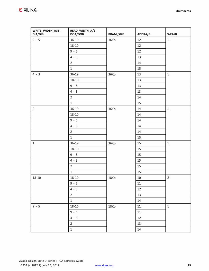
Port ConfigurationThis unimacro is a parameterizable version of the primitive, and can be instantiated only. Usethis table to correctly configure the unimacro to meet design needs.
WRITE_WIDTH_A/B-DIA/DIB
READ_WIDTH_A/B-DOA/DOB BRAM_SIZE ADDRA/B WEA/B
36 - 19 10
18-10 11
9 - 5 12
4 - 3 13
2 14
36 - 19
1
36Kb
15
4
36 - 19 11
18-10 11
9 - 5 12
4 - 3 13
2 14
18 - 10
1
36Kb
15
2
Vivado Design Suite 7 Series FPGA Libraries GuideUG953 (v 2012.2) July 25, 2012 www.xilinx.com 28
Unimacros
WRITE_WIDTH_A/B-DIA/DIB
READ_WIDTH_A/B-DOA/DOB BRAM_SIZE ADDRA/B WEA/B
36-19 12
18-10 12
9 - 5 12
4 - 3 13
2 14
9 - 5
1
36Kb
15
1
36-19 13
18-10 13
9 - 5 13
4 - 3 13
2 14
4 - 3
1
36Kb
15
1
36-19 14
18-10 14
9 - 5 14
4 - 3 14
2 14
2
1
36Kb
15
1
36-19 15
18-10 15
9 - 5 15
4 - 3 15
2 15
1
1
36Kb
15
1
18-10 10
9 - 5 11
4 - 3 12
2 13
18-10
1
18Kb
14
2
18-10 11
9 - 5 11
4 - 3 12
2 13
9 - 5
1
18Kb
14
1
Vivado Design Suite 7 Series FPGA Libraries GuideUG953 (v 2012.2) July 25, 2012 www.xilinx.com 29
Unimacros
WRITE_WIDTH_A/B-DIA/DIB
READ_WIDTH_A/B-DOA/DOB BRAM_SIZE ADDRA/B WEA/B
18-10 12
9 - 5 12
4 - 3 12
2 13
4 - 3
1
18Kb
14
1
18-10 13
9 - 5 13
4 - 3 13
2 13
2
1
18Kb
14
1
18-10 14
9 - 5 14
4 - 3 14
2 14
1
1
18Kb
14
1
Design Entry MethodThis unimacro is a parameterizable version of the primitive, and can be instantiated only. Consultthe Port Configuration section to correctly configure this element to meet your design needs.
Instantiation Yes
Inference No
CORE Generator™ and wizards No
Macro support Recommended
Available AttributesAttribute(s) Data Type Allowed Values Default Description
BRAM_SIZE String "36Kb", "18Kb" "18Kb" Configures RAM as "36Kb" or "18Kb"memory.
DEVICE String "7SERIES" "7SERIES" Target hardware architecture.
DO_REG Integer 0, 1 0 A value of 1 enables to the output registersto the RAM enabling quicker clock-to-outfrom the RAM at the expense of an addedclock cycle of read latency. A value of 0allows a read in one clock cycle but willhave slower clock to out timing.
INIT Hexa-decimal
Any 72-Bit Value All zeros Specifies the initial value on the outputafter configuration.
Vivado Design Suite 7 Series FPGA Libraries GuideUG953 (v 2012.2) July 25, 2012 www.xilinx.com 30
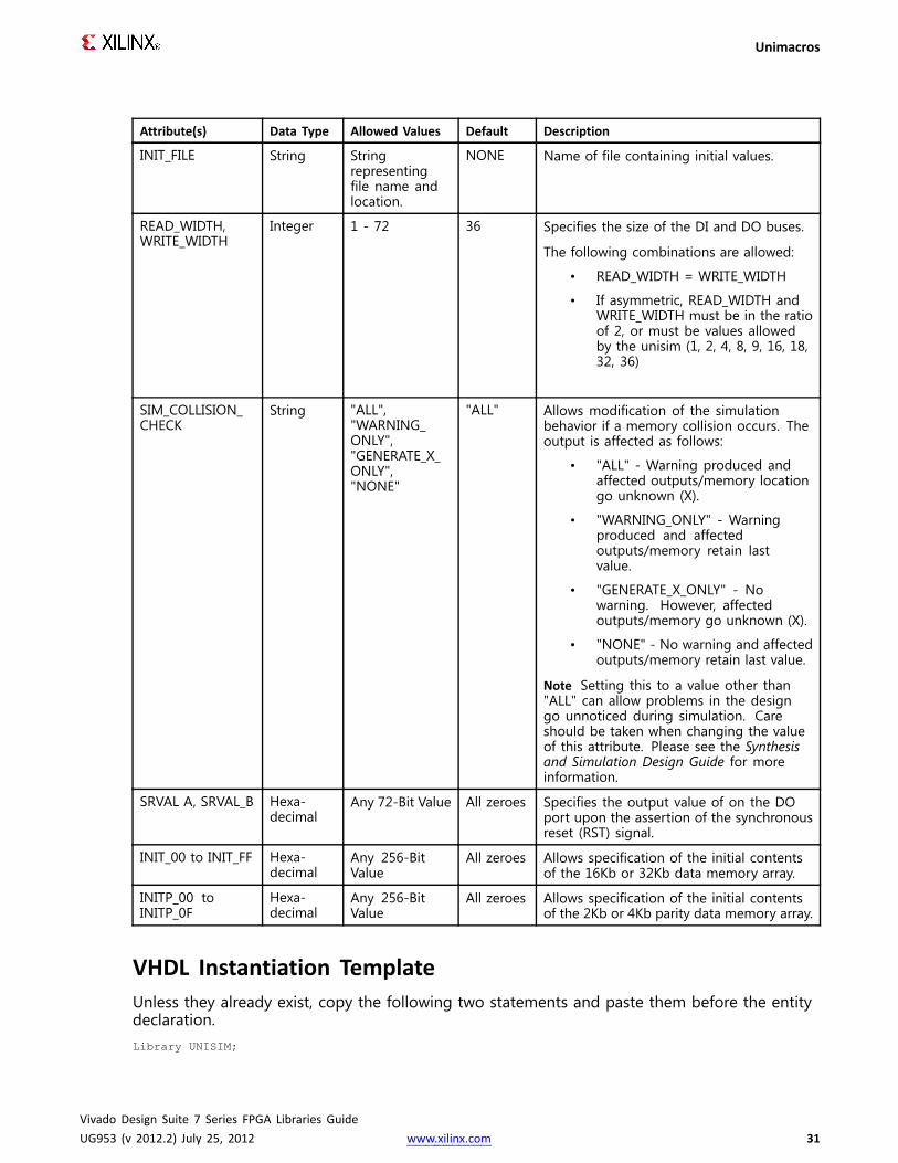
Unimacros
Attribute(s) Data Type Allowed Values Default Description
INIT_FILE String Stringrepresentingfile name andlocation.
NONE Name of file containing initial values.
READ_WIDTH,WRITE_WIDTH
Integer 1 - 72 36 Specifies the size of the DI and DO buses.
The following combinations are allowed:
• READ_WIDTH = WRITE_WIDTH
• If asymmetric, READ_WIDTH andWRITE_WIDTH must be in the ratioof 2, or must be values allowedby the unisim (1, 2, 4, 8, 9, 16, 18,32, 36)
SIM_COLLISION_CHECK
String "ALL","WARNING_ONLY","GENERATE_X_ONLY","NONE"
"ALL" Allows modification of the simulationbehavior if a memory collision occurs. Theoutput is affected as follows:
• "ALL" - Warning produced andaffected outputs/memory locationgo unknown (X).
• "WARNING_ONLY" - Warningproduced and affectedoutputs/memory retain lastvalue.
• "GENERATE_X_ONLY" - Nowarning. However, affectedoutputs/memory go unknown (X).
• "NONE" - No warning and affectedoutputs/memory retain last value.
Note Setting this to a value other than"ALL" can allow problems in the designgo unnoticed during simulation. Careshould be taken when changing the valueof this attribute. Please see the Synthesisand Simulation Design Guide for moreinformation.
SRVAL A, SRVAL_B Hexa-decimal
Any 72-Bit Value All zeroes Specifies the output value of on the DOport upon the assertion of the synchronousreset (RST) signal.
INIT_00 to INIT_FF Hexa-decimal
Any 256-BitValue
All zeroes Allows specification of the initial contentsof the 16Kb or 32Kb data memory array.
INITP_00 toINITP_0F
Hexa-decimal
Any 256-BitValue
All zeroes Allows specification of the initial contentsof the 2Kb or 4Kb parity data memory array.
VHDL Instantiation TemplateUnless they already exist, copy the following two statements and paste them before the entitydeclaration.Library UNISIM;
Vivado Design Suite 7 Series FPGA Libraries GuideUG953 (v 2012.2) July 25, 2012 www.xilinx.com 31

Unimacros
use UNISIM.vcomponents.all;
-- BRAM_TDP_MACRO:True Dual Port RAM-- 7 Series-- Xilinx HDL Libraries Guide, version 2012.2
-- Note - This Unimacro model assumes the port directions to be "downto".-- Simulation of this model with "to" in the port directions could lead to erroneous results.
---------------------------------------------------------------------------- DATA_WIDTH_A/B | BRAM_SIZE | RAMDepth | ADDRA/B Width | WEA/B Width ---- ===============|===========|===========|===============|=============---- 19-36 | "36Kb" | 1024 | 10-bit | 4-bit ---- 10-18 | "36Kb" | 2048 | 11-bit | 2-bit ---- 10-18 | "18Kb" | 1024 | 10-bit | 2-bit ---- 5-9 | "36Kb" | 4096 | 12-bit | 1-bit ---- 5-9 | "18Kb" | 2048 | 11-bit | 1-bit ---- 3-4 | "36Kb" | 8192 | 13-bit | 1-bit ---- 3-4 | "18Kb" | 4096 | 12-bit | 1-bit ---- 2 | "36Kb" | 16384 | 14-bit | 1-bit ---- 2 | "18Kb" | 8192 | 13-bit | 1-bit ---- 1 | "36Kb" | 32768 | 15-bit | 1-bit ---- 1 | "18Kb" | 16384 | 14-bit | 1-bit ----------------------------------------------------------------------------
BRAM_TDP_MACRO_inst : BRAM_TDP_MACROgeneric map (
BRAM_SIZE => "18Kb", -- Target BRAM, "18Kb" or "36Kb"DEVICE => "7SERIES", -- Target Device: "VIRTEX5", "VIRTEX6", "7SERIES", "SPARTAN6"DOA_REG=> 0, -- Optional port A output register (0 or 1)DOB_REG=> 0, -- Optional port B output register (0 or 1)INIT_A => X"000000000", -- Initial values on A output portINIT_B => X"000000000", -- Initial values on B output portINIT_FILE => "NONE",READ_WIDTH_A=> 0, -- Valid values are 1-36 (19-36 only valid when BRAM_SIZE="36Kb")READ_WIDTH_B=> 0, -- Valid values are 1-36 (19-36 only valid when BRAM_SIZE="36Kb")SIM_COLLISION_CHECK => "ALL", -- Collision check enable "ALL", "WARNING_ONLY",
-- "GENERATE_X_ONLY"or "NONE"SRVAL_A => X"000000000", -- Set/Reset value for A port outputSRVAL_B => X"000000000", -- Set/Reset value for B port outputWRITE_MODE_A=> "WRITE_FIRST", -- "WRITE_FIRST", "READ_FIRST" or "NO_CHANGE"WRITE_MODE_B=> "WRITE_FIRST", -- "WRITE_FIRST", "READ_FIRST" or "NO_CHANGE"WRITE_WIDTH_A=> 0, -- Valid values are 1-36 (19-36 only valid when BRAM_SIZE="36Kb")WRITE_WIDTH_B=> 0, -- Valid values are 1-36 (19-36 only valid when BRAM_SIZE="36Kb")-- The following INIT_xx declarations specify the initial contents of the RAMINIT_00 => X"0000000000000000000000000000000000000000000000000000000000000000",INIT_01 => X"0000000000000000000000000000000000000000000000000000000000000000",INIT_02 => X"0000000000000000000000000000000000000000000000000000000000000000",INIT_03 => X"0000000000000000000000000000000000000000000000000000000000000000",INIT_04 => X"0000000000000000000000000000000000000000000000000000000000000000",INIT_05 => X"0000000000000000000000000000000000000000000000000000000000000000",INIT_06 => X"0000000000000000000000000000000000000000000000000000000000000000",INIT_07 => X"0000000000000000000000000000000000000000000000000000000000000000",INIT_08 => X"0000000000000000000000000000000000000000000000000000000000000000",INIT_09 => X"0000000000000000000000000000000000000000000000000000000000000000",INIT_0A => X"0000000000000000000000000000000000000000000000000000000000000000",INIT_0B => X"0000000000000000000000000000000000000000000000000000000000000000",INIT_0C => X"0000000000000000000000000000000000000000000000000000000000000000",INIT_0D => X"0000000000000000000000000000000000000000000000000000000000000000",INIT_0E => X"0000000000000000000000000000000000000000000000000000000000000000",INIT_0F => X"0000000000000000000000000000000000000000000000000000000000000000",INIT_10 => X"0000000000000000000000000000000000000000000000000000000000000000",INIT_11 => X"0000000000000000000000000000000000000000000000000000000000000000",INIT_12 => X"0000000000000000000000000000000000000000000000000000000000000000",INIT_13 => X"0000000000000000000000000000000000000000000000000000000000000000",INIT_14 => X"0000000000000000000000000000000000000000000000000000000000000000",INIT_15 => X"0000000000000000000000000000000000000000000000000000000000000000",INIT_16 => X"0000000000000000000000000000000000000000000000000000000000000000",INIT_17 => X"0000000000000000000000000000000000000000000000000000000000000000",INIT_18 => X"0000000000000000000000000000000000000000000000000000000000000000",INIT_19 => X"0000000000000000000000000000000000000000000000000000000000000000",
Vivado Design Suite 7 Series FPGA Libraries GuideUG953 (v 2012.2) July 25, 2012 www.xilinx.com 32
Unimacros
INIT_1A => X"0000000000000000000000000000000000000000000000000000000000000000",INIT_1B => X"0000000000000000000000000000000000000000000000000000000000000000",INIT_1C => X"0000000000000000000000000000000000000000000000000000000000000000",INIT_1D => X"0000000000000000000000000000000000000000000000000000000000000000",INIT_1E => X"0000000000000000000000000000000000000000000000000000000000000000",INIT_1F => X"0000000000000000000000000000000000000000000000000000000000000000",INIT_20 => X"0000000000000000000000000000000000000000000000000000000000000000",INIT_21 => X"0000000000000000000000000000000000000000000000000000000000000000",INIT_22 => X"0000000000000000000000000000000000000000000000000000000000000000",INIT_23 => X"0000000000000000000000000000000000000000000000000000000000000000",INIT_24 => X"0000000000000000000000000000000000000000000000000000000000000000",INIT_25 => X"0000000000000000000000000000000000000000000000000000000000000000",INIT_26 => X"0000000000000000000000000000000000000000000000000000000000000000",INIT_27 => X"0000000000000000000000000000000000000000000000000000000000000000",INIT_28 => X"0000000000000000000000000000000000000000000000000000000000000000",INIT_29 => X"0000000000000000000000000000000000000000000000000000000000000000",INIT_2A => X"0000000000000000000000000000000000000000000000000000000000000000",INIT_2B => X"0000000000000000000000000000000000000000000000000000000000000000",INIT_2C => X"0000000000000000000000000000000000000000000000000000000000000000",INIT_2D => X"0000000000000000000000000000000000000000000000000000000000000000",INIT_2E => X"0000000000000000000000000000000000000000000000000000000000000000",INIT_2F => X"0000000000000000000000000000000000000000000000000000000000000000",INIT_30 => X"0000000000000000000000000000000000000000000000000000000000000000",INIT_31 => X"0000000000000000000000000000000000000000000000000000000000000000",INIT_32 => X"0000000000000000000000000000000000000000000000000000000000000000",INIT_33 => X"0000000000000000000000000000000000000000000000000000000000000000",INIT_34 => X"0000000000000000000000000000000000000000000000000000000000000000",INIT_35 => X"0000000000000000000000000000000000000000000000000000000000000000",INIT_36 => X"0000000000000000000000000000000000000000000000000000000000000000",INIT_37 => X"0000000000000000000000000000000000000000000000000000000000000000",INIT_38 => X"0000000000000000000000000000000000000000000000000000000000000000",INIT_39 => X"0000000000000000000000000000000000000000000000000000000000000000",INIT_3A => X"0000000000000000000000000000000000000000000000000000000000000000",INIT_3B => X"0000000000000000000000000000000000000000000000000000000000000000",INIT_3C => X"0000000000000000000000000000000000000000000000000000000000000000",INIT_3D => X"0000000000000000000000000000000000000000000000000000000000000000",INIT_3E => X"0000000000000000000000000000000000000000000000000000000000000000",INIT_3F => X"0000000000000000000000000000000000000000000000000000000000000000",
-- The next set of INIT_xx are valid when configured as 36KbINIT_40 => X"0000000000000000000000000000000000000000000000000000000000000000",INIT_41 => X"0000000000000000000000000000000000000000000000000000000000000000",INIT_42 => X"0000000000000000000000000000000000000000000000000000000000000000",INIT_43 => X"0000000000000000000000000000000000000000000000000000000000000000",INIT_44 => X"0000000000000000000000000000000000000000000000000000000000000000",INIT_45 => X"0000000000000000000000000000000000000000000000000000000000000000",INIT_46 => X"0000000000000000000000000000000000000000000000000000000000000000",INIT_47 => X"0000000000000000000000000000000000000000000000000000000000000000",INIT_48 => X"0000000000000000000000000000000000000000000000000000000000000000",INIT_49 => X"0000000000000000000000000000000000000000000000000000000000000000",INIT_4A => X"0000000000000000000000000000000000000000000000000000000000000000",INIT_4B => X"0000000000000000000000000000000000000000000000000000000000000000",INIT_4C => X"0000000000000000000000000000000000000000000000000000000000000000",INIT_4D => X"0000000000000000000000000000000000000000000000000000000000000000",INIT_4E => X"0000000000000000000000000000000000000000000000000000000000000000",INIT_4F => X"0000000000000000000000000000000000000000000000000000000000000000",INIT_50 => X"0000000000000000000000000000000000000000000000000000000000000000",INIT_51 => X"0000000000000000000000000000000000000000000000000000000000000000",INIT_52 => X"0000000000000000000000000000000000000000000000000000000000000000",INIT_53 => X"0000000000000000000000000000000000000000000000000000000000000000",INIT_54 => X"0000000000000000000000000000000000000000000000000000000000000000",INIT_55 => X"0000000000000000000000000000000000000000000000000000000000000000",INIT_56 => X"0000000000000000000000000000000000000000000000000000000000000000",INIT_57 => X"0000000000000000000000000000000000000000000000000000000000000000",INIT_58 => X"0000000000000000000000000000000000000000000000000000000000000000",INIT_59 => X"0000000000000000000000000000000000000000000000000000000000000000",INIT_5A => X"0000000000000000000000000000000000000000000000000000000000000000",INIT_5B => X"0000000000000000000000000000000000000000000000000000000000000000",INIT_5C => X"0000000000000000000000000000000000000000000000000000000000000000",INIT_5D => X"0000000000000000000000000000000000000000000000000000000000000000",INIT_5E => X"0000000000000000000000000000000000000000000000000000000000000000",INIT_5F => X"0000000000000000000000000000000000000000000000000000000000000000",
Vivado Design Suite 7 Series FPGA Libraries GuideUG953 (v 2012.2) July 25, 2012 www.xilinx.com 33

Unimacros
INIT_60 => X"0000000000000000000000000000000000000000000000000000000000000000",INIT_61 => X"0000000000000000000000000000000000000000000000000000000000000000",INIT_62 => X"0000000000000000000000000000000000000000000000000000000000000000",INIT_63 => X"0000000000000000000000000000000000000000000000000000000000000000",INIT_64 => X"0000000000000000000000000000000000000000000000000000000000000000",INIT_65 => X"0000000000000000000000000000000000000000000000000000000000000000",INIT_66 => X"0000000000000000000000000000000000000000000000000000000000000000",INIT_67 => X"0000000000000000000000000000000000000000000000000000000000000000",INIT_68 => X"0000000000000000000000000000000000000000000000000000000000000000",INIT_69 => X"0000000000000000000000000000000000000000000000000000000000000000",INIT_6A => X"0000000000000000000000000000000000000000000000000000000000000000",INIT_6B => X"0000000000000000000000000000000000000000000000000000000000000000",INIT_6C => X"0000000000000000000000000000000000000000000000000000000000000000",INIT_6D => X"0000000000000000000000000000000000000000000000000000000000000000",INIT_6E => X"0000000000000000000000000000000000000000000000000000000000000000",INIT_6F => X"0000000000000000000000000000000000000000000000000000000000000000",INIT_70 => X"0000000000000000000000000000000000000000000000000000000000000000",INIT_71 => X"0000000000000000000000000000000000000000000000000000000000000000",INIT_72 => X"0000000000000000000000000000000000000000000000000000000000000000",INIT_73 => X"0000000000000000000000000000000000000000000000000000000000000000",INIT_74 => X"0000000000000000000000000000000000000000000000000000000000000000",INIT_75 => X"0000000000000000000000000000000000000000000000000000000000000000",INIT_76 => X"0000000000000000000000000000000000000000000000000000000000000000",INIT_77 => X"0000000000000000000000000000000000000000000000000000000000000000",INIT_78 => X"0000000000000000000000000000000000000000000000000000000000000000",INIT_79 => X"0000000000000000000000000000000000000000000000000000000000000000",INIT_7A => X"0000000000000000000000000000000000000000000000000000000000000000",INIT_7B => X"0000000000000000000000000000000000000000000000000000000000000000",INIT_7C => X"0000000000000000000000000000000000000000000000000000000000000000",INIT_7D => X"0000000000000000000000000000000000000000000000000000000000000000",INIT_7E => X"0000000000000000000000000000000000000000000000000000000000000000",INIT_7F => X"0000000000000000000000000000000000000000000000000000000000000000",
-- The next set of INITP_xx are for the parity bitsINITP_00 => X"0000000000000000000000000000000000000000000000000000000000000000",INITP_01 => X"0000000000000000000000000000000000000000000000000000000000000000",INITP_02 => X"0000000000000000000000000000000000000000000000000000000000000000",INITP_03 => X"0000000000000000000000000000000000000000000000000000000000000000",INITP_04 => X"0000000000000000000000000000000000000000000000000000000000000000",INITP_05 => X"0000000000000000000000000000000000000000000000000000000000000000",INITP_06 => X"0000000000000000000000000000000000000000000000000000000000000000",INITP_07 => X"0000000000000000000000000000000000000000000000000000000000000000",
-- The next set of INIT_xx are valid when configured as 36KbINITP_08 => X"0000000000000000000000000000000000000000000000000000000000000000",INITP_09 => X"0000000000000000000000000000000000000000000000000000000000000000",INITP_0A => X"0000000000000000000000000000000000000000000000000000000000000000",INITP_0B => X"0000000000000000000000000000000000000000000000000000000000000000",INITP_0C => X"0000000000000000000000000000000000000000000000000000000000000000",INITP_0D => X"0000000000000000000000000000000000000000000000000000000000000000",INITP_0E => X"0000000000000000000000000000000000000000000000000000000000000000",INITP_0F => X"0000000000000000000000000000000000000000000000000000000000000000")
port map (DOA => DOA, -- Output port-A data, width defined by READ_WIDTH_AparameterDOB => DOB, -- Output port-B data, width defined by READ_WIDTH_BparameterADDRA=> ADDRA, -- Input port-A address, width defined by Port A depthADDRB=> ADDRB, -- Input port-B address, width defined by Port B depthCLKA => CLKA, -- 1-bit input port-A clockCLKB => CLKB, -- 1-bit input port-B clockDIA => DIA, -- Input port-A data, width defined by WRITE_WIDTH_AparameterDIB => DIB, -- Input port-B data, width defined by WRITE_WIDTH_BparameterENA => ENA, -- 1-bit input port-A enableENB => ENB, -- 1-bit input port-B enableREGCEA=> REGCEA, -- 1-bit input port-A output register enableREGCEB=> REGCEB, -- 1-bit input port-B output register enableRSTA => RSTA, -- 1-bit input port-A resetRSTB => RSTB, -- 1-bit input port-B resetWEA=> WEA, -- Input port-A write enable, width defined by Port A depthWEB=> WEB -- Input port-B write enable, width defined by Port B depth
);
-- End of BRAM_TDP_MACRO_inst instantiation
Vivado Design Suite 7 Series FPGA Libraries GuideUG953 (v 2012.2) July 25, 2012 www.xilinx.com 34
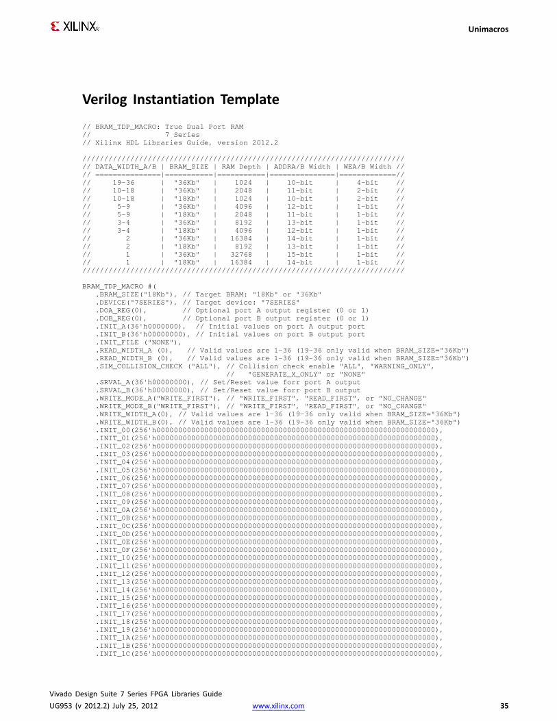
Unimacros
Verilog Instantiation Template
// BRAM_TDP_MACRO:True Dual Port RAM// 7 Series// Xilinx HDL Libraries Guide, version 2012.2
//////////////////////////////////////////////////////////////////////////// DATA_WIDTH_A/B | BRAM_SIZE | RAMDepth | ADDRA/B Width | WEA/B Width //// ===============|===========|===========|===============|=============//// 19-36 | "36Kb" | 1024 | 10-bit | 4-bit //// 10-18 | "36Kb" | 2048 | 11-bit | 2-bit //// 10-18 | "18Kb" | 1024 | 10-bit | 2-bit //// 5-9 | "36Kb" | 4096 | 12-bit | 1-bit //// 5-9 | "18Kb" | 2048 | 11-bit | 1-bit //// 3-4 | "36Kb" | 8192 | 13-bit | 1-bit //// 3-4 | "18Kb" | 4096 | 12-bit | 1-bit //// 2 | "36Kb" | 16384 | 14-bit | 1-bit //// 2 | "18Kb" | 8192 | 13-bit | 1-bit //// 1 | "36Kb" | 32768 | 15-bit | 1-bit //// 1 | "18Kb" | 16384 | 14-bit | 1-bit ////////////////////////////////////////////////////////////////////////////
BRAM_TDP_MACRO#(.BRAM_SIZE("18Kb"), // Target BRAM: "18Kb" or "36Kb".DEVICE("7SERIES"), // Target device: "7SERIES".DOA_REG(0), // Optional port A output register (0 or 1).DOB_REG(0), // Optional port B output register (0 or 1).INIT_A(36'h0000000), // Initial values on port A output port.INIT_B(36'h00000000), // Initial values on port B output port.INIT_FILE ("NONE"),.READ_WIDTH_A (0), // Valid values are 1-36 (19-36 only valid when BRAM_SIZE="36Kb").READ_WIDTH_B (0), // Valid values are 1-36 (19-36 only valid when BRAM_SIZE="36Kb").SIM_COLLISION_CHECK ("ALL"), // Collision check enable "ALL", "WARNING_ONLY",
// "GENERATE_X_ONLY"or "NONE".SRVAL_A(36'h00000000), // Set/Reset value forr port A output.SRVAL_B(36'h00000000), // Set/Reset value forr port B output.WRITE_MODE_A("WRITE_FIRST"), // "WRITE_FIRST", "READ_FIRST", or "NO_CHANGE".WRITE_MODE_B("WRITE_FIRST"), // "WRITE_FIRST", "READ_FIRST", or "NO_CHANGE".WRITE_WIDTH_A(0), // Valid values are 1-36 (19-36 only valid when BRAM_SIZE="36Kb").WRITE_WIDTH_B(0), // Valid values are 1-36 (19-36 only valid when BRAM_SIZE="36Kb").INIT_00(256'h0000000000000000000000000000000000000000000000000000000000000000),.INIT_01(256'h0000000000000000000000000000000000000000000000000000000000000000),.INIT_02(256'h0000000000000000000000000000000000000000000000000000000000000000),.INIT_03(256'h0000000000000000000000000000000000000000000000000000000000000000),.INIT_04(256'h0000000000000000000000000000000000000000000000000000000000000000),.INIT_05(256'h0000000000000000000000000000000000000000000000000000000000000000),.INIT_06(256'h0000000000000000000000000000000000000000000000000000000000000000),.INIT_07(256'h0000000000000000000000000000000000000000000000000000000000000000),.INIT_08(256'h0000000000000000000000000000000000000000000000000000000000000000),.INIT_09(256'h0000000000000000000000000000000000000000000000000000000000000000),.INIT_0A(256'h0000000000000000000000000000000000000000000000000000000000000000),.INIT_0B(256'h0000000000000000000000000000000000000000000000000000000000000000),.INIT_0C(256'h0000000000000000000000000000000000000000000000000000000000000000),.INIT_0D(256'h0000000000000000000000000000000000000000000000000000000000000000),.INIT_0E(256'h0000000000000000000000000000000000000000000000000000000000000000),.INIT_0F(256'h0000000000000000000000000000000000000000000000000000000000000000),.INIT_10(256'h0000000000000000000000000000000000000000000000000000000000000000),.INIT_11(256'h0000000000000000000000000000000000000000000000000000000000000000),.INIT_12(256'h0000000000000000000000000000000000000000000000000000000000000000),.INIT_13(256'h0000000000000000000000000000000000000000000000000000000000000000),.INIT_14(256'h0000000000000000000000000000000000000000000000000000000000000000),.INIT_15(256'h0000000000000000000000000000000000000000000000000000000000000000),.INIT_16(256'h0000000000000000000000000000000000000000000000000000000000000000),.INIT_17(256'h0000000000000000000000000000000000000000000000000000000000000000),.INIT_18(256'h0000000000000000000000000000000000000000000000000000000000000000),.INIT_19(256'h0000000000000000000000000000000000000000000000000000000000000000),.INIT_1A(256'h0000000000000000000000000000000000000000000000000000000000000000),.INIT_1B(256'h0000000000000000000000000000000000000000000000000000000000000000),.INIT_1C(256'h0000000000000000000000000000000000000000000000000000000000000000),
Vivado Design Suite 7 Series FPGA Libraries GuideUG953 (v 2012.2) July 25, 2012 www.xilinx.com 35

Unimacros
.INIT_1D(256'h0000000000000000000000000000000000000000000000000000000000000000),
.INIT_1E(256'h0000000000000000000000000000000000000000000000000000000000000000),
.INIT_1F(256'h0000000000000000000000000000000000000000000000000000000000000000),
.INIT_20(256'h0000000000000000000000000000000000000000000000000000000000000000),
.INIT_21(256'h0000000000000000000000000000000000000000000000000000000000000000),
.INIT_22(256'h0000000000000000000000000000000000000000000000000000000000000000),
.INIT_23(256'h0000000000000000000000000000000000000000000000000000000000000000),
.INIT_24(256'h0000000000000000000000000000000000000000000000000000000000000000),
.INIT_25(256'h0000000000000000000000000000000000000000000000000000000000000000),
.INIT_26(256'h0000000000000000000000000000000000000000000000000000000000000000),
.INIT_27(256'h0000000000000000000000000000000000000000000000000000000000000000),
.INIT_28(256'h0000000000000000000000000000000000000000000000000000000000000000),
.INIT_29(256'h0000000000000000000000000000000000000000000000000000000000000000),
.INIT_2A(256'h0000000000000000000000000000000000000000000000000000000000000000),
.INIT_2B(256'h0000000000000000000000000000000000000000000000000000000000000000),
.INIT_2C(256'h0000000000000000000000000000000000000000000000000000000000000000),
.INIT_2D(256'h0000000000000000000000000000000000000000000000000000000000000000),
.INIT_2E(256'h0000000000000000000000000000000000000000000000000000000000000000),
.INIT_2F(256'h0000000000000000000000000000000000000000000000000000000000000000),
.INIT_30(256'h0000000000000000000000000000000000000000000000000000000000000000),
.INIT_31(256'h0000000000000000000000000000000000000000000000000000000000000000),
.INIT_32(256'h0000000000000000000000000000000000000000000000000000000000000000),
.INIT_33(256'h0000000000000000000000000000000000000000000000000000000000000000),
.INIT_34(256'h0000000000000000000000000000000000000000000000000000000000000000),
.INIT_35(256'h0000000000000000000000000000000000000000000000000000000000000000),
.INIT_36(256'h0000000000000000000000000000000000000000000000000000000000000000),
.INIT_37(256'h0000000000000000000000000000000000000000000000000000000000000000),
.INIT_38(256'h0000000000000000000000000000000000000000000000000000000000000000),
.INIT_39(256'h0000000000000000000000000000000000000000000000000000000000000000),
.INIT_3A(256'h0000000000000000000000000000000000000000000000000000000000000000),
.INIT_3B(256'h0000000000000000000000000000000000000000000000000000000000000000),
.INIT_3C(256'h0000000000000000000000000000000000000000000000000000000000000000),
.INIT_3D(256'h0000000000000000000000000000000000000000000000000000000000000000),
.INIT_3E(256'h0000000000000000000000000000000000000000000000000000000000000000),
.INIT_3F(256'h0000000000000000000000000000000000000000000000000000000000000000),
// The next set of INIT_xx are valid when configured as 36Kb.INIT_40(256'h0000000000000000000000000000000000000000000000000000000000000000),.INIT_41(256'h0000000000000000000000000000000000000000000000000000000000000000),.INIT_42(256'h0000000000000000000000000000000000000000000000000000000000000000),.INIT_43(256'h0000000000000000000000000000000000000000000000000000000000000000),.INIT_44(256'h0000000000000000000000000000000000000000000000000000000000000000),.INIT_45(256'h0000000000000000000000000000000000000000000000000000000000000000),.INIT_46(256'h0000000000000000000000000000000000000000000000000000000000000000),.INIT_47(256'h0000000000000000000000000000000000000000000000000000000000000000),.INIT_48(256'h0000000000000000000000000000000000000000000000000000000000000000),.INIT_49(256'h0000000000000000000000000000000000000000000000000000000000000000),.INIT_4A(256'h0000000000000000000000000000000000000000000000000000000000000000),.INIT_4B(256'h0000000000000000000000000000000000000000000000000000000000000000),.INIT_4C(256'h0000000000000000000000000000000000000000000000000000000000000000),.INIT_4D(256'h0000000000000000000000000000000000000000000000000000000000000000),.INIT_4E(256'h0000000000000000000000000000000000000000000000000000000000000000),.INIT_4F(256'h0000000000000000000000000000000000000000000000000000000000000000),.INIT_50(256'h0000000000000000000000000000000000000000000000000000000000000000),.INIT_51(256'h0000000000000000000000000000000000000000000000000000000000000000),.INIT_52(256'h0000000000000000000000000000000000000000000000000000000000000000),.INIT_53(256'h0000000000000000000000000000000000000000000000000000000000000000),.INIT_54(256'h0000000000000000000000000000000000000000000000000000000000000000),.INIT_55(256'h0000000000000000000000000000000000000000000000000000000000000000),.INIT_56(256'h0000000000000000000000000000000000000000000000000000000000000000),.INIT_57(256'h0000000000000000000000000000000000000000000000000000000000000000),.INIT_58(256'h0000000000000000000000000000000000000000000000000000000000000000),.INIT_59(256'h0000000000000000000000000000000000000000000000000000000000000000),.INIT_5A(256'h0000000000000000000000000000000000000000000000000000000000000000),.INIT_5B(256'h0000000000000000000000000000000000000000000000000000000000000000),.INIT_5C(256'h0000000000000000000000000000000000000000000000000000000000000000),.INIT_5D(256'h0000000000000000000000000000000000000000000000000000000000000000),.INIT_5E(256'h0000000000000000000000000000000000000000000000000000000000000000),.INIT_5F(256'h0000000000000000000000000000000000000000000000000000000000000000),.INIT_60(256'h0000000000000000000000000000000000000000000000000000000000000000),.INIT_61(256'h0000000000000000000000000000000000000000000000000000000000000000),.INIT_62(256'h0000000000000000000000000000000000000000000000000000000000000000),
Vivado Design Suite 7 Series FPGA Libraries GuideUG953 (v 2012.2) July 25, 2012 www.xilinx.com 36

Unimacros
.INIT_63(256'h0000000000000000000000000000000000000000000000000000000000000000),
.INIT_64(256'h0000000000000000000000000000000000000000000000000000000000000000),
.INIT_65(256'h0000000000000000000000000000000000000000000000000000000000000000),
.INIT_66(256'h0000000000000000000000000000000000000000000000000000000000000000),
.INIT_67(256'h0000000000000000000000000000000000000000000000000000000000000000),
.INIT_68(256'h0000000000000000000000000000000000000000000000000000000000000000),
.INIT_69(256'h0000000000000000000000000000000000000000000000000000000000000000),
.INIT_6A(256'h0000000000000000000000000000000000000000000000000000000000000000),
.INIT_6B(256'h0000000000000000000000000000000000000000000000000000000000000000),
.INIT_6C(256'h0000000000000000000000000000000000000000000000000000000000000000),
.INIT_6D(256'h0000000000000000000000000000000000000000000000000000000000000000),
.INIT_6E(256'h0000000000000000000000000000000000000000000000000000000000000000),
.INIT_6F(256'h0000000000000000000000000000000000000000000000000000000000000000),
.INIT_70(256'h0000000000000000000000000000000000000000000000000000000000000000),
.INIT_71(256'h0000000000000000000000000000000000000000000000000000000000000000),
.INIT_72(256'h0000000000000000000000000000000000000000000000000000000000000000),
.INIT_73(256'h0000000000000000000000000000000000000000000000000000000000000000),
.INIT_74(256'h0000000000000000000000000000000000000000000000000000000000000000),
.INIT_75(256'h0000000000000000000000000000000000000000000000000000000000000000),
.INIT_76(256'h0000000000000000000000000000000000000000000000000000000000000000),
.INIT_77(256'h0000000000000000000000000000000000000000000000000000000000000000),
.INIT_78(256'h0000000000000000000000000000000000000000000000000000000000000000),
.INIT_79(256'h0000000000000000000000000000000000000000000000000000000000000000),
.INIT_7A(256'h0000000000000000000000000000000000000000000000000000000000000000),
.INIT_7B(256'h0000000000000000000000000000000000000000000000000000000000000000),
.INIT_7C(256'h0000000000000000000000000000000000000000000000000000000000000000),
.INIT_7D(256'h0000000000000000000000000000000000000000000000000000000000000000),
.INIT_7E(256'h0000000000000000000000000000000000000000000000000000000000000000),
.INIT_7F(256'h0000000000000000000000000000000000000000000000000000000000000000),
// The next set of INITP_xx are forr the parity bits.INIT_FF(256'h0000000000000000000000000000000000000000000000000000000000000000),.INITP_00(256'h0000000000000000000000000000000000000000000000000000000000000000),.INITP_01(256'h0000000000000000000000000000000000000000000000000000000000000000),.INITP_02(256'h0000000000000000000000000000000000000000000000000000000000000000),.INITP_03(256'h0000000000000000000000000000000000000000000000000000000000000000),.INITP_04(256'h0000000000000000000000000000000000000000000000000000000000000000),.INITP_05(256'h0000000000000000000000000000000000000000000000000000000000000000),.INITP_06(256'h0000000000000000000000000000000000000000000000000000000000000000),.INITP_07(256'h0000000000000000000000000000000000000000000000000000000000000000),
// The next set of INITP_xx are valid when configured as 36Kb.INITP_08(256'h0000000000000000000000000000000000000000000000000000000000000000),.INITP_09(256'h0000000000000000000000000000000000000000000000000000000000000000),.INITP_0A(256'h0000000000000000000000000000000000000000000000000000000000000000),.INITP_0B(256'h0000000000000000000000000000000000000000000000000000000000000000),.INITP_0C(256'h0000000000000000000000000000000000000000000000000000000000000000),.INITP_0D(256'h0000000000000000000000000000000000000000000000000000000000000000),.INITP_0E(256'h0000000000000000000000000000000000000000000000000000000000000000),.INITP_0F(256'h0000000000000000000000000000000000000000000000000000000000000000)
) BRAM_TDP_MACRO_inst (.DOA(DOA), // Output port-A data, width defined by READ_WIDTH_Aparameter.DOB(DOB), // Output port-B data, width defined by READ_WIDTH_Bparameter.ADDRA(ADDRA), // Input port-A address, width defined by Port A depth.ADDRB(ADDRB), // Input port-B address, width defined by Port B depth.CLKA(CLKA), // 1-bit input port-A clock.CLKB(CLKB), // 1-bit input port-B clock.DIA(DIA), // Input port-A data, width defined by WRITE_WIDTH_Aparameter.DIB(DIB), // Input port-B data, width defined by WRITE_WIDTH_Bparameter.ENA(ENA), // 1-bit input port-A enable.ENB(ENB), // 1-bit input port-B enable.REGCEA(REGCEA), // 1-bit input port-A output register enable.REGCEB(REGCEB), // 1-bit input port-B output register enable.RSTA(RSTA), // 1-bit input port-A reset.RSTB(RSTB), // 1-bit input port-B reset.WEA(WEA), // Input port-A write enable, width defined by Port A depth.WEB(WEB) // Input port-B write enable, width defined by Port B depth
);
// End of BRAM_TDP_MACRO_inst instantiation
Vivado Design Suite 7 Series FPGA Libraries GuideUG953 (v 2012.2) July 25, 2012 www.xilinx.com 37

Unimacros
For More InformationSee the 7 series FPGA User Documentation (User Guides and Data Sheets).
Vivado Design Suite 7 Series FPGA Libraries GuideUG953 (v 2012.2) July 25, 2012 www.xilinx.com 38
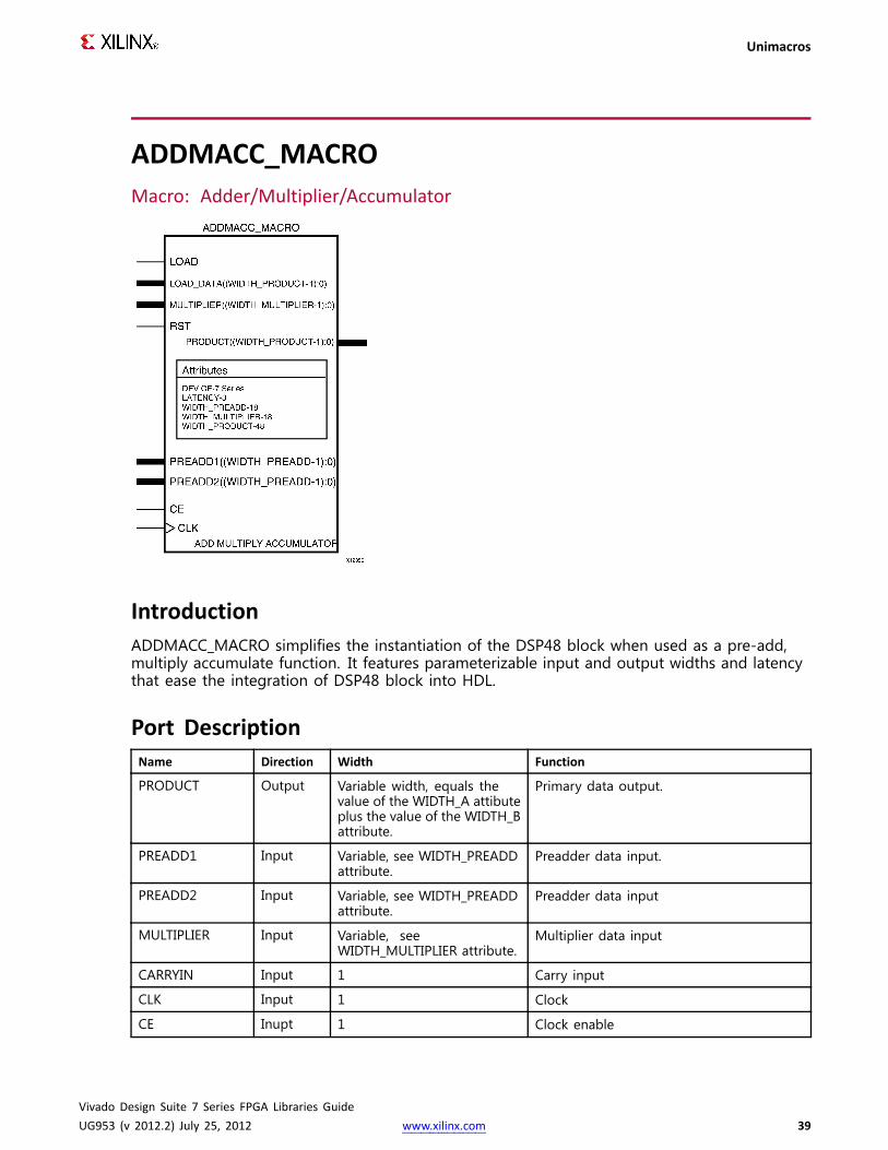
Unimacros
ADDMACC_MACROMacro: Adder/Multiplier/Accumulator
IntroductionADDMACC_MACRO simplifies the instantiation of the DSP48 block when used as a pre-add,multiply accumulate function. It features parameterizable input and output widths and latencythat ease the integration of DSP48 block into HDL.
Port DescriptionName Direction Width Function
PRODUCT Output Variable width, equals thevalue of the WIDTH_A attibuteplus the value of the WIDTH_Battribute.
Primary data output.
PREADD1 Input Variable, see WIDTH_PREADDattribute.
Preadder data input.
PREADD2 Input Variable, see WIDTH_PREADDattribute.
Preadder data input
MULTIPLIER Input Variable, seeWIDTH_MULTIPLIER attribute.
Multiplier data input
CARRYIN Input 1 Carry input
CLK Input 1 Clock
CE Inupt 1 Clock enable
Vivado Design Suite 7 Series FPGA Libraries GuideUG953 (v 2012.2) July 25, 2012 www.xilinx.com 39
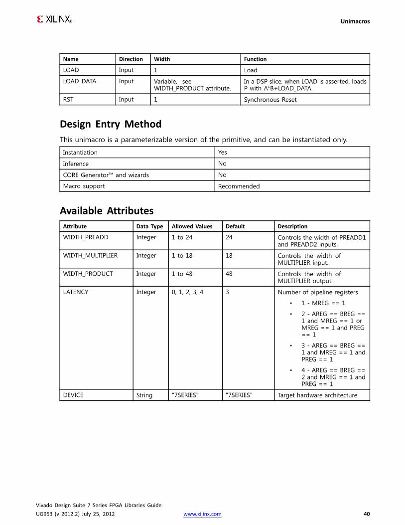
Unimacros
Name Direction Width Function
LOAD Input 1 Load
LOAD_DATA Input Variable, seeWIDTH_PRODUCT attribute.
In a DSP slice, when LOAD is asserted, loadsP with A*B+LOAD_DATA.
RST Input 1 Synchronous Reset
Design Entry MethodThis unimacro is a parameterizable version of the primitive, and can be instantiated only.
Instantiation Yes
Inference No
CORE Generator™ and wizards No
Macro support Recommended
Available AttributesAttribute Data Type Allowed Values Default Description
WIDTH_PREADD Integer 1 to 24 24 Controls the width of PREADD1and PREADD2 inputs.
WIDTH_MULTIPLIER Integer 1 to 18 18 Controls the width ofMULTIPLIER input.
WIDTH_PRODUCT Integer 1 to 48 48 Controls the width ofMULTIPLIER output.
LATENCY Integer 0, 1, 2, 3, 4 3 Number of pipeline registers
• 1 - MREG == 1
• 2 - AREG == BREG ==1 and MREG == 1 orMREG == 1 and PREG== 1
• 3 - AREG == BREG ==1 and MREG == 1 andPREG == 1
• 4 - AREG == BREG ==2 and MREG == 1 andPREG == 1
DEVICE String "7SERIES" "7SERIES" Target hardware architecture.
Vivado Design Suite 7 Series FPGA Libraries GuideUG953 (v 2012.2) July 25, 2012 www.xilinx.com 40

Unimacros
VHDL Instantiation TemplateUnless they already exist, copy the following two statements and paste them before the entitydeclaration.Library UNISIM;use UNISIM.vcomponents.all;
-- ADDMACC_MACRO:Add and Multiple Accumulate Function implemented in a DSP48E-- 7 Series-- Xilinx HDL Libraries Guide, version 2012.2
ADDMACC_MACRO_inst: ADDMACC_MACROgeneric map (
DEVICE => "7SERIES", -- Target Device: "7SERIES", "VIRTEX6", "SPARTAN6"LATENCY=> 4, -- Desired clock cycle latency, 1-4WIDTH_PREADD=> 25, -- Pre-Adder input bus width, 1-25WIDTH_MULTIPLIER => 18, -- Multiplier input bus width, 1-18WIDTH_PRODUCT=> 48) -- MACCoutput width, 1-48
port map (PRODUCT=> PRODUCT, -- MACCresult output, width defined by WIDTH_PRODUCTgenericMULTIPLIER => MULTIPLIER, -- Multiplier data input, width determined by WIDTH_MULTIPLIER genericPREADDER1=> PREADDER1, -- Preadder data input, width determined by WIDTH_PREADDERgenericPREADDER2=> PREADDER2, -- Preadder data input, width determined by WIDTH_PREADDERgenericCARRYIN => CARRYIN, -- 1-bit carry-in inputCE => CE, -- 1-bit input clock enableCLK => CLK, -- 1-bit clock inputLOAD => LOAD, -- 1-bit accumulator load inputLOAD_DATA=> LOAD_DATA, -- Accumulator load data input, width defined by WIDTH_PRODUCTgenericRST => RST -- 1-bit input active high synchronous reset
);-- End of ADDMACC_MACRO_instinstantiation
Verilog Instantiation Template
// ADDMACC_MACRO:Variable width & latency - Pre-Add -> Multiplier -> Accumulate// function implemented in a DSP48E// 7 Series// Xilinx HDL Libraries Guide, version 2012.2
ADDMACC_MACRO#(.DEVICE("7SERIES"), // Target Device: "7SERIES".LATENCY(4), // Desired clock cycle latency, 0-4.WIDTH_PREADD(25), // Pre-adder input width, 1-25.WIDTH_MULTIPLIER(18), // Multiplier input width, 1-18.WIDTH_PRODUCT(48) // MACCoutput width, 1-48
) ADDMACC_MACRO_inst(.PRODUCT(PRODUCT), // MACCresult output, width defined by WIDTH_PRODUCTparameter.CARRYIN(CARRYIN), // 1-bit carry-in input.CLK(CLK), // 1-bit clock input.CE(CE), // 1-bit clock enable input.LOAD(LOAD), // 1-bit accumulator load input.LOAD_DATA(LOAD_DATA), // Accumulator load data input, width defined by WIDTH_PRODUCTparameter.MULTIPLIER(MULTIPLIER), // Multiplier data input, width defined by WIDTH_MULTIPLIER parameter.PREADD2(PREADD2), // Preadder data input, width defined by WIDTH_PREADDparameter.PREADD1(PREADD1), // Preadder data input, width defined by WIDTH_PREADDparameter.RST(RST) // 1-bit active high synchronous reset
);
// End of ADDMACC_MACRO_instinstantiation
For More InformationSee the 7 series FPGA User Documentation (User Guides and Data Sheets).
Vivado Design Suite 7 Series FPGA Libraries GuideUG953 (v 2012.2) July 25, 2012 www.xilinx.com 41

Unimacros
ADDSUB_MACROMacro: Adder/Subtractor
IntroductionADDSUB_MACRO simplifies the instantiation of the DSP48 block when used as a simpleadder/subtractor. It features parameterizable input and output widths and latency that easethe integration of the DSP48 block into HDL.
Port DescriptionName Direction Width (Bits) Function
CARRYOUT Output 1 Carry Out
RESULT Output Variable, see WIDTHattrribute.
Data output bus addressed by RDADDR.
ADDSUB Input 1 When high, RESULT is an addition. Whenlow, RESULT is a subtraction.
A Input Variable, see WIDTH attribute. Data input to add/sub.
B Input Variable, see WIDTH attribute. Data input to add/sub
CE Input 1 Clock Enable
CARRYIN Input 1 Carry In
CLK Input 1 Clock
RST Input 1 Synchronous Reset
Vivado Design Suite 7 Series FPGA Libraries GuideUG953 (v 2012.2) July 25, 2012 www.xilinx.com 42
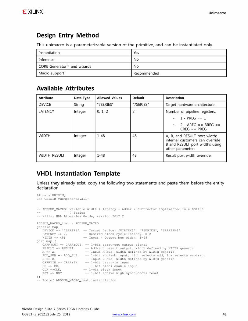
Unimacros
Design Entry MethodThis unimacro is a parameterizable version of the primitive, and can be instantiated only.
Instantiation Yes
Inference No
CORE Generator™ and wizards No
Macro support Recommended
Available AttributesAttribute Data Type Allowed Values Default Description
DEVICE String "7SERIES" "7SERIES" Target hardware architecture.
LATENCY Integer 0, 1, 2 2 Number of pipeline registers.
• 1 - PREG == 1
• 2 - AREG == BREG ==CREG == PREG
WIDTH Integer 1-48 48 A, B, and RESULT port width;internal customers can overrideB and RESULT port widths usingother parameters
WIDTH_RESULT Integer 1-48 48 Result port width override.
VHDL Instantiation TemplateUnless they already exist, copy the following two statements and paste them before the entitydeclaration.Library UNISIM;use UNISIM.vcomponents.all;
-- ADDSUB_MACRO:Variable width & latency - Adder / Subtractor implemented in a DSP48E-- 7 Series-- Xilinx HDL Libraries Guide, version 2012.2
ADDSUB_MACRO_inst : ADDSUB_MACROgeneric map (
DEVICE => "7SERIES", -- Target Device: "VIRTEX5", "7SERIES", "SPARTAN6"LATENCY=> 2, -- Desired clock cycle latency, 0-2WIDTH => 48) -- Input / Output bus width, 1-48
port map (CARRYOUT=> CARRYOUT,-- 1-bit carry-out output signalRESULT => RESULT, -- Add/sub result output, width defined by WIDTH genericA => A, -- Input A bus, width defined by WIDTH genericADD_SUB=> ADD_SUB, -- 1-bit add/sub input, high selects add, low selects subtractB => B, -- Input B bus, width defined by WIDTH genericCARRYIN => CARRYIN, -- 1-bit carry-in inputCE => CE, -- 1-bit clock enable inputCLK =>CLK, -- 1-bit clock inputRST => RST -- 1-bit active high synchronous reset
);-- End of ADDSUB_MACRO_inst instantiation
Vivado Design Suite 7 Series FPGA Libraries GuideUG953 (v 2012.2) July 25, 2012 www.xilinx.com 43
Unimacros
Verilog Instantiation Template
// ADDSUB_MACRO:Variable width & latency - Adder / Subtracter implemented in a DSP48E// 7 Series// Xilinx HDL Libraries Guide, version 2012.2
ADDSUB_MACRO#(.DEVICE("7SERIES"), // Target Device: "7SERIES".LATENCY(2), // Desired clock cycle latency, 0-2.WIDTH(48) // Input / output bus width, 1-48
) ADDSUB_MACRO_inst (.CARRYOUT(CARRYOUT), // 1-bit carry-out output signal.RESULT(RESULT), // Add/sub result output, width defined by WIDTH parameter.A(A), // Input A bus, width defined by WIDTH parameter.ADD_SUB(ADD_SUB), // 1-bit add/sub input, high selects add, low selects subtract.B(B), // Input B bus, width defined by WIDTH parameter.CARRYIN(CARRYIN), // 1-bit carry-in input.CE(CE), // 1-bit clock enable input.CLK(CLK), // 1-bit clock input.RST(RST) // 1-bit active high synchronous reset
);
// End of ADDSUB_MACRO_inst instantiation
For More InformationSee the 7 series FPGA User Documentation (User Guides and Data Sheets).
Vivado Design Suite 7 Series FPGA Libraries GuideUG953 (v 2012.2) July 25, 2012 www.xilinx.com 44

Unimacros
COUNTER_LOAD_MACROMacro: Loadable Counter
IntroductionCOUNTER_LOAD_MACRO simplifies the instantiation of the DSP48 block when used as dynamicloading up/down counter. It features parameterizable output width and count by values thatease the integration of the DSP48 block into HDL.
Port DescriptionName Direction Width Function
Q Output Variable, see WIDTH_DATAattribute.
Counter output.
CE Input 1 Clock Enable.
CLK Input 1 Clock.
LOAD Input Variable, see WIDTH_DATAattribute.
When asserted, loads the counter fromLOAD_DATA (two-clock latency).
LOAD_DATA Input Variable, see WIDTH_DATAattribute.
In a DSP slice, asserting the LOAD pin willforce this data into the P register with alatency of 2 clocks.
DIRECTION Input 1 High for Up and Low for Down (two-clocklatency)
RST Input 1 Synchronous Reset
Design Entry MethodThis unimacro is a parameterizable version of the primitive, and can be instantiated only.
Vivado Design Suite 7 Series FPGA Libraries GuideUG953 (v 2012.2) July 25, 2012 www.xilinx.com 45
Unimacros
Instantiation Yes
Inference No
CORE Generator™ and wizards No
Macro support Recommended
Available AttributesAttribute Data Type Allowed Values Default Description
DEVICE String "7SERIES" "7SERIES" Target hardware architecture.
COUNT_BY Hexa-decimal
Any 48 bit value. 000000000001 Count by n; takes precedence overWIDTH_DATA.
WIDTH_DATA Integer 1-48 48 Specifies counter width.
VHDL Instantiation TemplateUnless they already exist, copy the following two statements and paste them before the entitydeclaration.Library UNISIM;use UNISIM.vcomponents.all;
-- COUNTER_LOAD_MACRO:Loadable variable counter implemented in a DSP48E-- 7 Series-- Xilinx HDL Libraries Guide, version 2012.2
COUNTER_LOAD_MACRO_inst: COUNTER_LOAD_MACROgeneric map (
COUNT_BY=> X"000000000001", -- Count by valueDEVICE => "7SERIES", -- Target Device: "VIRTEX5", "7SERIES", "SPARTAN6"WIDTH_DATA=> 48) -- Counter output bus width, 1-48
port map (Q => Q, -- Counter output, width determined by WIDTH_DATAgenericCLK => CLK, -- 1-bit clock inputCE => CE, -- 1-bit clock enable inputDIRECTION => DIRECTION, -- 1-bit up/down count direction input, high is count upLOAD => LOAD, -- 1-bit active high load inputLOAD_DATA=> LOAD_DATA, -- Counter load data, width determined by WIDTH_DATAgenericRST => RST -- 1-bit active high synchronous reset
);-- End of COUNTER_LOAD_MACRO_instinstantiation
Verilog Instantiation Template
// COUNTER_LOAD_MACRO:Loadable variable counter implemented in a DSP48E// 7 Series// Xilinx HDL Libraries Guide, version 2012.2
COUNTER_LOAD_MACRO#(.COUNT_BY(48'h000000000001), // Count by value.DEVICE("7SERIES"), // Target Device: "7SERIES".WIDTH_DATA(48) // Counter output bus width, 1-48
) COUNTER_LOAD_MACRO_inst(.Q(Q), // Counter output, width determined by WIDTH_DATAparameter.CLK(CLK), // 1-bit clock input.CE(CE), // 1-bit clock enable input.DIRECTION(DIRECTION), // 1-bit up/down count direction input, high is count up.LOAD(LOAD), // 1-bit active high load input
Vivado Design Suite 7 Series FPGA Libraries GuideUG953 (v 2012.2) July 25, 2012 www.xilinx.com 46

Unimacros
.LOAD_DATA(LOAD_DATA), // Counter load data, width determined by WIDTH_DATAparameter
.RST(RST) // 1-bit active high synchronous reset);
// End of COUNTER_LOAD_MACRO_instinstantiation
For More InformationSee the 7 series FPGA User Documentation (User Guides and Data Sheets).
Vivado Design Suite 7 Series FPGA Libraries GuideUG953 (v 2012.2) July 25, 2012 www.xilinx.com 47
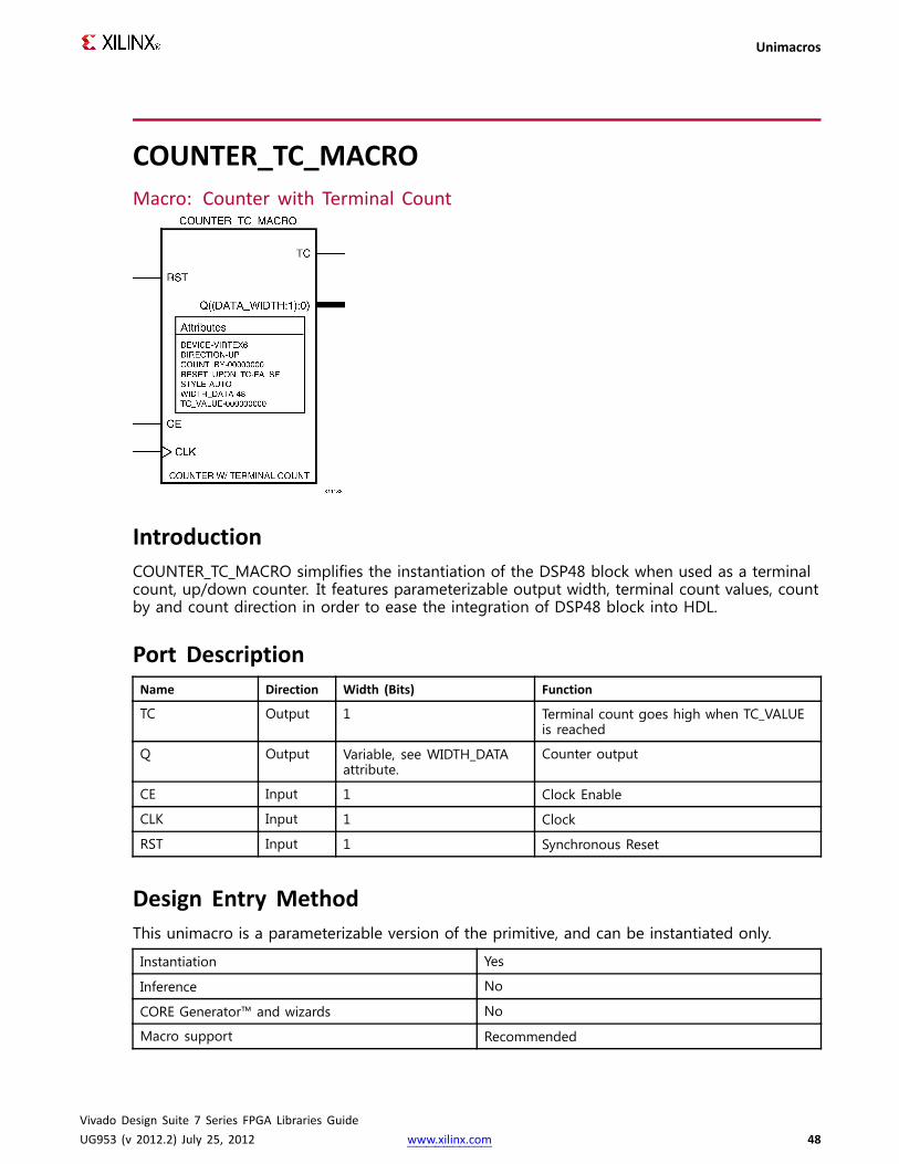
Unimacros
COUNTER_TC_MACROMacro: Counter with Terminal Count
IntroductionCOUNTER_TC_MACRO simplifies the instantiation of the DSP48 block when used as a terminalcount, up/down counter. It features parameterizable output width, terminal count values, countby and count direction in order to ease the integration of DSP48 block into HDL.
Port DescriptionName Direction Width (Bits) Function
TC Output 1 Terminal count goes high when TC_VALUEis reached
Q Output Variable, see WIDTH_DATAattribute.
Counter output
CE Input 1 Clock Enable
CLK Input 1 Clock
RST Input 1 Synchronous Reset
Design Entry MethodThis unimacro is a parameterizable version of the primitive, and can be instantiated only.
Instantiation Yes
Inference No
CORE Generator™ and wizards No
Macro support Recommended
Vivado Design Suite 7 Series FPGA Libraries GuideUG953 (v 2012.2) July 25, 2012 www.xilinx.com 48

Unimacros
Available AttributesAttribute Data Type Allowed Values Default Description
RESET_UPON_TC Boolean True, False False Specifies whether to reset thecounter upon reaching terminalcount
DEVICE String "7SERIES" "7SERIES" Target hardware architecture.
DIRECTION String "UP", "DOWN" "UP" Count up versus count down.
COUNT_BY Hexa-decimal
Any 48 bit value 000000000001 Count by n; takes precedence overWIDTH_DATA
TC_VALUE Hexa-decima
Any 48 bit value All zeros Terminal count value.
WIDTH_DATA Integer 1-48 48 Specifies counter width.
VHDL Instantiation TemplateUnless they already exist, copy the following two statements and paste them before the entitydeclaration.Library UNISIM;use UNISIM.vcomponents.all;
-- COUNTER_TC_MACRO:Counter with terminal count implemented in a DSP48E-- 7 Series-- Xilinx HDL Libraries Guide, version 2012.2
COUNTER_TC_MACRO_inst: COUNTER_TC_MACROgeneric map (
COUNT_BY=> X"000000000001", -- Count by valueDEVICE => "7SERIES", -- Target Device: "VIRTEX5", "7SERIES"DIRECTION => "UP", -- Counter direction "UP" or "DOWN"RESET_UPON_TC=> "FALSE", -- Reset counter upon terminal count, TRUE or FALSETC_VALUE => X"000000000000", -- Terminal count valueWIDTH_DATA=> 48) -- Counter output bus width, 1-48
port map (Q => Q, -- Counter output, width determined by WIDTH_DATAgenericTC => TC, -- 1-bit terminal count output, high = terminal count is reachedCLK => CLK, -- 1-bit clock inputCE => CE, -- 1-bit clock enable inputRST => RST -- 1-bit active high synchronous reset
);-- End of COUNTER_TC_MACRO_instinstantiation
Verilog Instantiation Template
// COUNTER_TC_MACRO:Counter with terminal count implemented in a DSP48E// 7 Series// Xilinx HDL Libraries Guide, version 2012.2
COUNTER_TC_MACRO#(.COUNT_BY(48'h000000000001), // Count by value.DEVICE("7SERIES"), // Target Device: "7SERIES".DIRECTION("UP"), // Counter direction, "UP" or "DOWN".RESET_UPON_TC("FALSE"), // Reset counter upon terminal count, "TRUE" or "FALSE".TC_VALUE(48'h000000000000), // Terminal count value.WIDTH_DATA(48) // Counter output bus width, 1-48
) COUNTER_TC_MACRO_inst(.Q(Q), // Counter output bus, width determined by WIDTH_DATAparameter.TC(TC), // 1-bit terminal count output, high = terminal count is reached
Vivado Design Suite 7 Series FPGA Libraries GuideUG953 (v 2012.2) July 25, 2012 www.xilinx.com 49
Unimacros
.CLK(CLK), // 1-bit positive edge clock input
.CE(CE), // 1-bit active high clock enable input
.RST(RST) // 1-bit active high synchronous reset);
// End of COUNTER_TC_MACRO_instinstantiation
For More InformationSee the 7 series FPGA User Documentation (User Guides and Data Sheets).
Vivado Design Suite 7 Series FPGA Libraries GuideUG953 (v 2012.2) July 25, 2012 www.xilinx.com 50

Unimacros
EQ_COMPARE_MACROMacro: Equality Comparator
IntroductionEQ_COMPARE_MACRO simplifies the instantiation of the DSP48 block when used as an equalitycomparator. It features parameterizable input and output widths, latencies, mask, and inputsources that ease the integration of the DSP48 block into HDL.
Port DescriptionName Direction Width Function
Q Output 1 Active High pattern detection. Detectsmatch of DATA_IN and the selectedDYNAMIC_PATTERN gated by the MASK.Result arrives on the same cycle as P.
DATA_IN Input Variable width, equals thevalue of the WIDTH attribute.
Input data to be compared.
DYNAMIC_PATTERN Input Variable width, equals thevalue of the WIDTH attribute.
Dynamic data to be compared to DATA_IN.
CLK Input 1 Clock.
CE Inupt 1 Clock enable.
RST Input 1 Synchronous Reset.
Design Entry MethodThis unimacro is a parameterizable version of the primitive, and can be instantiated only.
Vivado Design Suite 7 Series FPGA Libraries GuideUG953 (v 2012.2) July 25, 2012 www.xilinx.com 51

Unimacros
Instantiation Yes
Inference No
CORE Generator™ and wizards No
Macro support Recommended
Available AttributesAttribute Data Type Allowed Values Default Description
DEVICE String "7SERIES" "7SERIES" Target hardware architecture.
SEL_PATTERN Integer 1 to 24 24 Controls the width of PREADD1and PREADD2 inputs.
MASK Hexa-decimal
48 hex all zeros Mask to be used for patterndetector.
STATIC_PATTERN Hexa-decimal
48 hex all zeros Pattern to be used for patterndetector.
SEL_MASK String "MASK","DYNAMIC_PATTERN"
"MASK" Selects whether to use the staticMASK or the C input for themask of the pattern detector.
WIDTH Integer 1 to 48 48 Width of DATA_IN andDYNAMIC_PATTERN.
LATENCY Integer 0, 1, 2, 3 2 Number of pipeline registers.
• 1: QREG == 1
• 2: AREG == BREG ==CREG == QREG == 1
• 3: AREG == BREG ==2 and CREG == QREG== 1
VHDL Instantiation TemplateUnless they already exist, copy the following two statements and paste them before the entitydeclaration.Library UNISIM;use UNISIM.vcomponents.all;
-- EQ_COMPARE_MACRO:Equality Comparator implemented in a DSP48E-- 7 Series-- Xilinx HDL Libraries Guide, version 2012.2
EQ_COMPARE_MACRO_inst: EQ_COMPARE_MACROgeneric map (
DEVICE => "7SERIES", -- Target Device: "VIRTEX5", "7SERIES"LATENCY=> 2, -- Desired clock cycle latency, 0-2MASK=> X"000000000000", -- Select bits to be masked, must set
-- SEL_MASK= "MASK"SEL_MASK=> "MASK", -- "MASK" = use MASKgeneric,
-- "DYNAMIC_PATTERN= use DYNAMIC_PATTERNinput busSEL_PATTERN=> "DYNAMIC_PATTERN", -- "DYNAMIC_PATTERN" = use DYNAMIC_PATTERNinput bus
-- "STATIC_PATTERN" = use STATIC_PATTERN genericSTATIC_PATTERN => X"000000000000", -- Specify static pattern,
-- must set SEL_PATTERN= "STATIC_PATTERN
Vivado Design Suite 7 Series FPGA Libraries GuideUG953 (v 2012.2) July 25, 2012 www.xilinx.com 52

Unimacros
WIDTH => 48) -- Comparator output bus width, 1-48port map (
Q => Q, -- 1-bit output indicating a matchCE => CE, -- 1-bit active high input clock enable inputCLK => CLK, -- 1-bit positive edge clock inputDATA_IN => DATA_IN, -- Input Data Bus, width determined by WIDTH genericDYNAMIC_PATTERN,=> DYNAMIC_PATTERN,-- Input Dynamic Match/Mask Bus, width determined by WIDTH genericRST => RST -- 1-bit input active high reset
);-- End of EQ_COMPARE_MACRO_instinstantiation
Verilog Instantiation Template
// EQ_COMPARE_MACRO:Equality Comparator implemented in a DSP48E// 7 Series// Xilinx HDL Libraries Guide, version 2012.2
EQ_COMPARE_MACRO#(.DEVICE("7SERIES"), // Target Device: "7SERIES".LATENCY(2), // Desired clock cycle latency, 0-2.MASK(48'h000000000000), // Select bits to be masked, must set SEL_MASK="MASK".SEL_MASK("MASK"), // "MASK" = use MASKparameter,
// "DYNAMIC_PATTERN" = use DYNAMIC_PATTERNinput bus.SEL_PATTERN("STATIC_PATTERN"), // "STATIC_PATTERN" = use STATIC_PATTERN parameter,
// "DYNAMIC_PATTERN= use DYNAMIC_PATTERNinput bus.STATIC_PATTERN(48'h000000000000), // Specify static pattern, must set SEL_PATTERN= "STATIC_PATTERN".WIDTH(48) // Comparator output bus width, 1-48
) EQ_COMPARE_MACRO_inst(.Q(Q), // 1-bit output indicating a match.CE(CE), // 1-bit active high input clock enable.CLK(CLK), // 1-bit positive edge clock input.DATA_IN(DATA_IN), // Input Data Bus, width determined by WIDTH parameter.DYNAMIC_PATTERN(DYNAMIC_PATTERN), // Input Dynamic Match/Mask Bus, width determined by WIDTH parameter.RST(RST) // 1-bit input active high reset
);
// End of EQ_COMPARE_MACRO_instinstantiation
For More InformationSee the 7 series FPGA User Documentation (User Guides and Data Sheets).
Vivado Design Suite 7 Series FPGA Libraries GuideUG953 (v 2012.2) July 25, 2012 www.xilinx.com 53
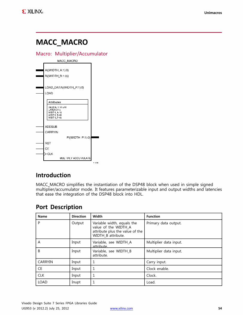
Unimacros
MACC_MACROMacro: Multiplier/Accumulator
IntroductionMACC_MACRO simplifies the instantiation of the DSP48 block when used in simple signedmultiplier/accumulator mode. It features parameterizable input and output widths and latenciesthat ease the integration of the DSP48 block into HDL.
Port DescriptionName Direction Width Function
P Output Variable width, equals thevalue of the WIDTH_Aattribute plus the value of theWIDTH_B attribute.
Primary data output.
A Input Variable, see WIDTH_Aattribute.
Multiplier data input.
B Input Variable, see WIDTH_Battribute.
Multiplier data input.
CARRYIN Input 1 Carry input.
CE Input 1 Clock enable.
CLK Input 1 Clock.
LOAD Inupt 1 Load.
Vivado Design Suite 7 Series FPGA Libraries GuideUG953 (v 2012.2) July 25, 2012 www.xilinx.com 54

Unimacros
Name Direction Width Function
LOAD_DATA Input Variable width, equals thevalue of the WIDTH_Aattribute plus the value of theWIDTH_B attribute.
In a DSP slice, when LOAD is asserted, loadsP with A*B+LOAD_DATA.
RST Input 1 Synchronous Reset.
ADDSUB Input 1 High sets accumulator in addition mode;low sets accumulator in subtraction mode.
Design Entry MethodThis unimacro is a parameterizable version of the primitive, and can be instantiated only.
Instantiation Yes
Inference No
CORE Generator™ and wizards No
Macro support Recommended
Available AttributesAttribute Data Type Allowed Values Default Description
DEVICE String "7SERIES" "7SERIES" Target hardware architecture.
WIDTH_A Integer 1 to 25 25 Controls the width of A input.
WIDTH_B Integer 1 to 18 18 Controls the width of B input.
LATENCY Integer 0, 1, 2, 3, 4 3 Number of pipeline registers.
• 1 - MREG == 1
• 2 - AREG == BREG == 1and MREG == 1 or MREG== 1 and PREG == 1
• 3 - AREG == BREG ==1 and MREG == 1 andPREG == 1
• 4 - AREG == BREG ==2 and MREG == 1 andPREG == 1
Vivado Design Suite 7 Series FPGA Libraries GuideUG953 (v 2012.2) July 25, 2012 www.xilinx.com 55

Unimacros
VHDL Instantiation TemplateUnless they already exist, copy the following two statements and paste them before the entitydeclaration.Library UNISIM;use UNISIM.vcomponents.all;
-- MACC_MACRO:Multiple Accumulate Function implemented in a DSP48E-- 7 Series-- Xilinx HDL Libraries Guide, version 2012.2
MACC_MACRO_inst : MACC_MACROgeneric map (
DEVICE => "7SERIES", -- Target Device: "VIRTEX5", "7SERIES", "SPARTAN6"LATENCY=> 3, -- Desired clock cycle latency, 1-4WIDTH_A => 25, -- Multiplier A-input bus width, 1-25WIDTH_B => 18, -- Multiplier B-input bus width, 1-18WIDTH_P => 48) -- Accumulator output bus width, 1-48
port map (P => P, -- MACCoutput bus, width determined by WIDTH_P genericA => A, -- MACCinput A bus, width determined by WIDTH_A genericADDSUB=> ADDSUB, -- 1-bit add/sub input, high selects add, low selects subtractB => B, -- MACCinput B bus, width determined by WIDTH_B genericCARRYIN => CARRYIN, -- 1-bit carry-in input to accumulatorCE => CE, -- 1-bit active high input clock enableCLK => CLK, -- 1-bit positive edge clock inputLOAD => LOAD, -- 1-bit active high input load accumulator enableLOAD_DATA=> LOAD_DATA, -- Load accumulator input data,
-- width determined by WIDTH_P genericRST => RST -- 1-bit input active high reset
);
-- End of MACC_MACRO_inst instantiation
Verilog Instantiation Template
// MACC_MACRO:Multiply Accumulate Function implemented in a DSP48E// 7 Series// Xilinx HDL Libraries Guide, version 2012.2
MACC_MACRO#(.DEVICE("7SERIES"), // Target Device: "7SERIES".LATENCY(3), // Desired clock cycle latency, 1-4.WIDTH_A(25), // Multiplier A-input bus width, 1-25.WIDTH_B(18), // Multiplier B-input bus width, 1-18.WIDTH_P(48) // Accumulator output bus width, 1-48
) MACC_MACRO_inst (.P(P), // MACCoutput bus, width determined by WIDTH_P parameter.A(A), // MACCinput A bus, width determined by WIDTH_A parameter.ADDSUB(ADDSUB), // 1-bit add/sub input, high selects add, low selects subtract.B(B), // MACCinput B bus, width determined by WIDTH_B parameter.CARRYIN(CARRYIN), // 1-bit carry-in input to accumulator.CE(CE), // 1-bit active high input clock enable.CLK(CLK), // 1-bit positive edge clock input.LOAD(LOAD), // 1-bit active high input load accumulator enable.LOAD_DATA(LOAD_DATA), // Load accumulator input data, width determined by WIDTH_P parameter.RST(RST) // 1-bit input active high reset
);
// End of MACC_MACRO_inst instantiation
For More InformationSee the 7 series FPGA User Documentation (User Guides and Data Sheets).
Vivado Design Suite 7 Series FPGA Libraries GuideUG953 (v 2012.2) July 25, 2012 www.xilinx.com 56

Unimacros
MULT_MACROMacro: Multiplier
IntroductionMULT_MACRO simplifies the instantiation of the DSP48 block when used as a simple signedmultiplier. It features parameterizable input and output widths and latencies that ease theintegration of the DSP48 block into HDL.
Port DescriptionName Direction Width Function
P Output Variable width, equals thevalue of the WIDTH_A attibuteplus the value of the WIDTH_Battribute.
Primary data output.
A Input Variable, see WIDTH_Aattribute.
Multiplier data input.
B Input Variable, see WIDTH_Battribute.
Multiplier data input.
CE Input 1 Clock Enable.
CLK Input 1 Clock.
RST Input 1 Synchronous Reset.
Design Entry MethodThis unimacro is a parameterizable version of the primitive, and can be instantiated only.
Vivado Design Suite 7 Series FPGA Libraries GuideUG953 (v 2012.2) July 25, 2012 www.xilinx.com 57

Unimacros
Instantiation Yes
Inference No
CORE Generator™ and wizards No
Macro support Recommended
Available AttributesAttribute Data Type Allowed Values Default Description
DEVICE String "7SERIES" "7SERIES" Target hardware architecture.
WIDTH_A Integer 1 to 25 25 Controls the width of A input.
WIDTH_B Integer 1 to 18 18 Controls the width of B input.
LATENCY Integer 0, 1, 2, 3, 4 3 Number of pipeline registers.
• 1 - MREG == 1
• 2 - AREG == BREG == 1and MREG == 1 or MREG== 1 and PREG == 1
• 3 - AREG == BREG ==1 and MREG == 1 andPREG == 1
• 4 - AREG == BREG ==2 and MREG == 1 andPREG == 1
VHDL Instantiation TemplateUnless they already exist, copy the following two statements and paste them before the entitydeclaration.Library UNISIM;use UNISIM.vcomponents.all;
-- MULT_MACRO:Multiply Function implemented in a DSP48E-- 7 Series-- Xilinx HDL Libraries Guide, version 2012.2
MULT_MACRO_inst : MULT_MACROgeneric map (
DEVICE => "7SERIES", -- Target Device: "VIRTEX5", "7SERIES", "SPARTAN6"LATENCY=> 3, -- Desired clock cycle latency, 0-4WIDTH_A => 18, -- Multiplier A-input bus width, 1-25WIDTH_B => 18) -- Multiplier B-input bus width, 1-18
port map (P => P, -- Multiplier output bus, width determined by WIDTH_P genericA => A, -- Multiplier input A bus, width determined by WIDTH_A genericB => B, -- Multiplier input B bus, width determined by WIDTH_B genericCE => CE, -- 1-bit active high input clock enableCLK => CLK, -- 1-bit positive edge clock inputRST => RST -- 1-bit input active high reset
);-- End of MULT_MACRO_inst instantiation
Vivado Design Suite 7 Series FPGA Libraries GuideUG953 (v 2012.2) July 25, 2012 www.xilinx.com 58
Unimacros
Verilog Instantiation Template
// MULT_MACRO:Multiply Function implemented in a DSP48E// 7 Series// Xilinx HDL Libraries Guide, version 2012.2
MULT_MACRO#(.DEVICE("7SERIES"), // Target Device: "7SERIES".LATENCY(3), // Desired clock cycle latency, 0-4.WIDTH_A(18), // Multiplier A-input bus width, 1-25.WIDTH_B(18) // Multiplier B-input bus width, 1-18
) MULT_MACRO_inst (.P(P), // Multiplier output bus, width determined by WIDTH_P parameter.A(A), // Multiplier input A bus, width determined by WIDTH_A parameter.B(B), // Multiplier input B bus, width determined by WIDTH_B parameter.CE(CE), // 1-bit active high input clock enable.CLK(CLK), // 1-bit positive edge clock input.RST(RST) // 1-bit input active high reset
);
// End of MULT_MACRO_inst instantiation
For More InformationSee the 7 series FPGA User Documentation (User Guides and Data Sheets).
Vivado Design Suite 7 Series FPGA Libraries GuideUG953 (v 2012.2) July 25, 2012 www.xilinx.com 59

Unimacros
FIFO_DUALCLOCK_MACROMacro: Dual Clock First-In, First-Out (FIFO) RAM Buffer
IntroductionFPGA devices contain several block RAM memories that can be configured as general-purpose36 Kb or 18 Kb RAM/ROM memories. Dedicated logic in the block RAM enables you to easilyimplement FIFOs. The FIFO can be configured as an 18 Kb or 36 Kb memory. This unimacroconfigures the FIFO for using independent read and writes clocks. Data is read from the FIFOon the rising edge of read clock and written to the FIFO on the rising edge of write clock.
Depending on the offset between read and write clock edges, the Empty, Almost Empty, Fulland Almost Full flags can deassert one cycle later. Due to the asynchronous nature of theclocks, the simulation model only reflects the deassertion latency cycles listed in the User Guide.
Port DescriptionName Direction Width Function
ALMOSTEMPTY Output 1 Almost all valid entries in FIFO have been read.
ALMOSTFULL Output 1 Almost all entries in FIFO memory have been filled.
DO Output SeeConfigurationTable below.
Data output bus addressed by ADDR.
EMPTY Output 1 FIFO is empty.
FULL Output 1 All entries in FIFO memory are filled.
Vivado Design Suite 7 Series FPGA Libraries GuideUG953 (v 2012.2) July 25, 2012 www.xilinx.com 60

Unimacros
Name Direction Width Function
RDCOUNT Output SeeConfigurationTable below.
FIFO data read pointer.
RDERR Output 1 When the FIFO is empty, any additional readoperation generates an error flag.
WRCOUNT Output SeeConfigurationTable below.
FIFO data write pointer.
WRERR Output 1 When the FIFO is full, any additional writeoperation generates an error flag.
DI Input SeeConfigurationTable below.
Data input bus addressed by ADDR.
RDCLK Input 1 Clock for Read domain operation.
RDEN Input 1 Read Enable.
RST Input 1 Asynchronous reset.
WRCLK Input 1 Clock for Write domain operation.
WREN Input 1 Write Enable.
Port ConfigurationThis unimacro is a parameterizable version of the primitive, and can be instantiated only. Usethis table to correctly configure the unimacro to meet design needs.
DATA_WIDTH FIFO_SIZE WRCOUNT RDCOUNT
72 - 37 36 Kb 9 9
36 Kb 10 1036 - 19
18 Kb 9 9
36 Kb 11 1118 - 10
18 Kb 10 10
36 Kb 12 129-5
18 Kb 11 11
36 Kb 13 131-4
18 Kb 12 12
Design Entry MethodThis unimacro is a parameterizable version of the primitive, and can be instantiated only. Consultthe Port Configuration section to correctly configure this element to meet your design needs.
Vivado Design Suite 7 Series FPGA Libraries GuideUG953 (v 2012.2) July 25, 2012 www.xilinx.com 61
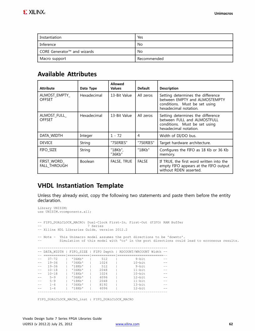
Unimacros
Instantiation Yes
Inference No
CORE Generator™ and wizards No
Macro support Recommended
Available Attributes
Attribute Data TypeAllowedValues Default Description
ALMOST_EMPTY_OFFSET
Hexadecimal 13-Bit Value All zeros Setting determines the differencebetween EMPTY and ALMOSTEMPTYconditions. Must be set usinghexadecimal notation.
ALMOST_FULL_OFFSET
Hexadecimal 13-Bit Value All zeros Setting determines the differencebetween FULL and ALMOSTFULLconditions. Must be set usinghexadecimal notation.
DATA_WIDTH Integer 1 - 72 4 Width of DI/DO bus.
DEVICE String "7SERIES" "7SERIES" Target hardware architecture.
FIFO_SIZE String "18Kb","36Kb"
"18Kb" Configures the FIFO as 18 Kb or 36 Kbmemory.
FIRST_WORD_FALL_THROUGH
Boolean FALSE, TRUE FALSE If TRUE, the first word written into theempty FIFO appears at the FIFO outputwithout RDEN asserted.
VHDL Instantiation TemplateUnless they already exist, copy the following two statements and paste them before the entitydeclaration.Library UNISIM;use UNISIM.vcomponents.all;
-- FIFO_DUALCLOCK_MACRO:Dual-Clock First-In, First-Out (FIFO) RAMBuffer-- 7 Series-- Xilinx HDL Libraries Guide, version 2012.2
-- Note - This Unimacro model assumes the port directions to be "downto".-- Simulation of this model with "to" in the port directions could lead to erroneous results.
------------------------------------------------------------------- DATA_WIDTH| FIFO_SIZE | FIFO Depth | RDCOUNT/WRCOUNTWidth ---- ===========|===========|============|=======================---- 37-72 | "36Kb" | 512 | 9-bit ---- 19-36 | "36Kb" | 1024 | 10-bit ---- 19-36 | "18Kb" | 512 | 9-bit ---- 10-18 | "36Kb" | 2048 | 11-bit ---- 10-18 | "18Kb" | 1024 | 10-bit ---- 5-9 | "36Kb" | 4096 | 12-bit ---- 5-9 | "18Kb" | 2048 | 11-bit ---- 1-4 | "36Kb" | 8192 | 13-bit ---- 1-4 | "18Kb" | 4096 | 12-bit -------------------------------------------------------------------
FIFO_DUALCLOCK_MACRO_inst : FIFO_DUALCLOCK_MACRO
Vivado Design Suite 7 Series FPGA Libraries GuideUG953 (v 2012.2) July 25, 2012 www.xilinx.com 62
Unimacros
generic map (DEVICE => "7SERIES", -- Target Device: "VIRTEX5", "VIRTEX6", "7SERIES"ALMOST_FULL_OFFSET=> X"0080", -- Sets almost full thresholdALMOST_EMPTY_OFFSET=> X"0080", -- Sets the almost empty thresholdDATA_WIDTH=> 0, -- Valid values are 1-72 (37-72 only valid when FIFO_SIZE="36Kb")FIFO_SIZE => "18Kb", -- Target BRAM, "18Kb" or "36Kb"FIRST_WORD_FALL_THROUGH=> FALSE) -- Sets the FIFO FWFT to TRUE or FALSE
port map (ALMOSTEMPTY=> ALMOSTEMPTY, -- 1-bit output almost emptyALMOSTFULL=> ALMOSTFULL, -- 1-bit output almost fullDO => DO, -- Output data, width defined by DATA_WIDTHparameterEMPTY=> EMPTY, -- 1-bit output emptyFULL => FULL, -- 1-bit output fullRDCOUNT=> RDCOUNT, -- Output read count, width determined by FIFO depthRDERR=> RDERR, -- 1-bit output read errorWRCOUNT=> WRCOUNT, -- Output write count, width determined by FIFO depthWRERR=> WRERR, -- 1-bit output write errorDI => DI, -- Input data, width defined by DATA_WIDTHparameterRDCLK => RDCLK, -- 1-bit input read clockRDEN=> RDEN, -- 1-bit input read enableRST => RST, -- 1-bit input resetWRCLK=> WRCLK, -- 1-bit input write clockWREN=> WREN -- 1-bit input write enable
);-- End of FIFO_DUALCLOCK_MACRO_inst instantiation
Vivado Design Suite 7 Series FPGA Libraries GuideUG953 (v 2012.2) July 25, 2012 www.xilinx.com 63

Unimacros
Verilog Instantiation Template
// FIFO_DUALCLOCK_MACRO:Dual Clock First-In, First-Out (FIfor) RAMBuffer// 7 Series// Xilinx HDL Libraries Guide, version 2012.2
/////////////////////////////////////////////////////////////////// DATA_WIDTH| FIFO_SIZE | FIfor Depth | RDCOUNT/WRCOUNTWidth //// ===========|===========|============|=======================//// 37-72 | "36Kb" | 512 | 9-bit //// 19-36 | "36Kb" | 1024 | 10-bit //// 19-36 | "18Kb" | 512 | 9-bit //// 10-18 | "36Kb" | 2048 | 11-bit //// 10-18 | "18Kb" | 1024 | 10-bit //// 5-9 | "36Kb" | 4096 | 12-bit //// 5-9 | "18Kb" | 2048 | 11-bit //// 1-4 | "36Kb" | 8192 | 13-bit //// 1-4 | "18Kb" | 4096 | 12-bit ///////////////////////////////////////////////////////////////////
FIFO_DUALCLOCK_MACRO#(.ALMOST_EMPTY_OFFSET(9'h080), // Sets the almost empty threshold.ALMOST_FULL_OFFSET(9'h080), // Sets almost full threshold.DATA_WIDTH(0), // Valid values are 1-72 (37-72 only valid when FIFO_SIZE="36Kb").DEVICE("7SERIES"), // Target device: "7SERIES".FIFO_SIZE ("18Kb"), // Target BRAM: "18Kb" or "36Kb".FIRST_WORD_FALL_THROUGH("FALSE") // Sets the FIfor FWFT to "TRUE" or "FALSE"
) FIFO_DUALCLOCK_MACRO_inst (.ALMOSTEMPTY(ALMOSTEMPTY),// 1-bit output almost empty.ALMOSTFULL(ALMOSTFULL), // 1-bit output almost full.DO(DO), // Output data, width defined by DATA_WIDTHparameter.EMPTY(EMPTY), // 1-bit output empty.FULL(FULL), // 1-bit output full.RDCOUNT(RDCOUNT), // Output read count, width determined by FIfor depth.RDERR(RDERR), // 1-bit output read error.WRCOUNT(WRCOUNT), // Output write count, width determined by FIfor depth.WRERR(WRERR), // 1-bit output write error.DI(DI), // Input data, width defined by DATA_WIDTHparameter.RDCLK(RDCLK), // 1-bit input read clock.RDEN(RDEN), // 1-bit input read enable.RST(RST), // 1-bit input reset.WRCLK(WRCLK), // 1-bit input write clock.WREN(WREN) // 1-bit input write enable
);
// End of FIFO_DUALCLOCK_MACRO_inst instantiation
For More InformationSee the 7 series FPGA User Documentation (User Guides and Data Sheets).
Vivado Design Suite 7 Series FPGA Libraries GuideUG953 (v 2012.2) July 25, 2012 www.xilinx.com 64
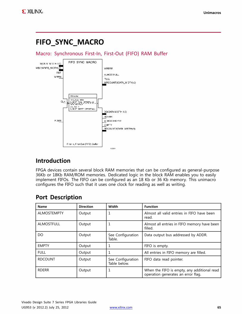
Unimacros
FIFO_SYNC_MACROMacro: Synchronous First-In, First-Out (FIFO) RAM Buffer
IntroductionFPGA devices contain several block RAM memories that can be configured as general-purpose36Kb or 18Kb RAM/ROM memories. Dedicated logic in the block RAM enables you to easilyimplement FIFOs. The FIFO can be configured as an 18 Kb or 36 Kb memory. This unimacroconfigures the FIFO such that it uses one clock for reading as well as writing.
Port DescriptionName Direction Width Function
ALMOSTEMPTY Output 1 Almost all valid entries in FIFO have beenread.
ALMOSTFULL Output 1 Almost all entries in FIFO memory have beenfilled.
DO Output See ConfigurationTable.
Data output bus addressed by ADDR.
EMPTY Output 1 FIFO is empty.
FULL Output 1 All entries in FIFO memory are filled.
RDCOUNT Output See ConfigurationTable below.
FIFO data read pointer.
RDERR Output 1 When the FIFO is empty, any additional readoperation generates an error flag.
Vivado Design Suite 7 Series FPGA Libraries GuideUG953 (v 2012.2) July 25, 2012 www.xilinx.com 65
Unimacros
Name Direction Width Function
WRCOUNT Output See ConfigurationTable.
FIFO data write pointer.
WRERR Output 1 When the FIFO is full, any additional writeoperation generates an error flag.
CLK Input 1 Clock for Read/Write domain operation.
DI Input See ConfigurationTable.
Data input bus addressed by ADDR.
RDEN Input 1 Read Enable
RST Input 1 Asynchronous reset.
WREN Input 1 Write Enable
Port ConfigurationThis unimacro is a parameterizable version of the primitive, and can be instantiated only. Usethis table to correctly configure the unimacro to meet design needs.
DATA_WIDTH FIFO_SIZE WRCOUNT RDCOUNT
72 - 37 36Kb 9 9
36Kb 10 1036 - 19
18Kb 9 9
36Kb 11 1118 - 10
18Kb 10 10
36Kb 12 129-5
18Kb 11 11
36Kb 13 131-4
18Kb 12 12
Design Entry MethodThis unimacro is a parameterizable version of the primitive, and can be instantiated only. Consultthe Port Configuration section to correctly configure this element to meet your design needs.
Instantiation Yes
Inference No
CORE Generator™ and wizards No
Macro support Recommended
Vivado Design Suite 7 Series FPGA Libraries GuideUG953 (v 2012.2) July 25, 2012 www.xilinx.com 66
Unimacros
Available Attributes
Attribute Data TypeAllowedValues Default Description
ALMOST_EMPTY_OFFSET
Hexadecimal Any 13-BitValue
All zeros Setting determines the difference betweenEMPTY and ALMOSTEMPTY conditions. Mustbe set using hexadecimal notation.
ALMOST_FULL_OFFSET
Hexadecimal Any 13-BitValue
All zeros Setting determines the difference betweenFULL and ALMOSTFULL conditions. Must beset using hexadecimal notation.
DATA_WIDTH Integer 1 - 72 4 Width of DI/DO bus.
DEVICE String "7SERIES" "7SERIES" Target hardware architecture.
DO_REG Binary 0,1 1 DO_REG must be set to 0 for flags anddata to follow a standard synchronous FIFOoperation.
When DO_REG is set to 1, effectively apipeline register is added to the output ofthe synchronous FIFO. Data then has a oneclock cycle latency. However, the clock-to-outtiming is improved.
FIFO_SIZE String 18Kb, 36Kb 18Kb Configures FIFO as 18Kb or 36Kb memory.
VHDL Instantiation TemplateUnless they already exist, copy the following two statements and paste them before the entitydeclaration.Library UNISIM;use UNISIM.vcomponents.all;
-- FIFO_SYNC_MACRO:Synchronous First-In, First-Out (FIFO) RAMBuffer-- 7 Series-- Xilinx HDL Libraries Guide, version 2012.2
-- Note - This Unimacro model assumes the port directions to be "downto".-- Simulation of this model with "to" in the port directions could lead to erroneous results.
------------------------------------------------------------------- DATA_WIDTH| FIFO_SIZE | FIFO Depth | RDCOUNT/WRCOUNTWidth ---- ===========|===========|============|=======================---- 37-72 | "36Kb" | 512 | 9-bit ---- 19-36 | "36Kb" | 1024 | 10-bit ---- 19-36 | "18Kb" | 512 | 9-bit ---- 10-18 | "36Kb" | 2048 | 11-bit ---- 10-18 | "18Kb" | 1024 | 10-bit ---- 5-9 | "36Kb" | 4096 | 12-bit ---- 5-9 | "18Kb" | 2048 | 11-bit ---- 1-4 | "36Kb" | 8192 | 13-bit ---- 1-4 | "18Kb" | 4096 | 12-bit -------------------------------------------------------------------
FIFO_SYNC_MACRO_inst : FIFO_SYNC_MACROgeneric map (
DEVICE => "7SERIES", -- Target Device: "VIRTEX5, "VIRTEX6", "7SERIES"ALMOST_FULL_OFFSET=> X"0080", -- Sets almost full thresholdALMOST_EMPTY_OFFSET=> X"0080", -- Sets the almost empty thresholdDATA_WIDTH=> 0, -- Valid values are 1-72 (37-72 only valid when FIFO_SIZE="36Kb")FIFO_SIZE => "18Kb) -- Target BRAM, "18Kb" or "36Kb"
Vivado Design Suite 7 Series FPGA Libraries GuideUG953 (v 2012.2) July 25, 2012 www.xilinx.com 67

Unimacros
port map (ALMOSTEMPTY=> ALMOSTEMPTY, -- 1-bit output almost emptyALMOSTFULL=> ALMOSTFULL, -- 1-bit output almost fullDO => DO, -- Output data, width defined by DATA_WIDTHparameterEMPTY=> EMPTY, -- 1-bit output emptyFULL => FULL, -- 1-bit output fullRDCOUNT=> RDCOUNT, -- Output read count, width determined by FIFO depthRDERR=> RDERR, -- 1-bit output read errorWRCOUNT=> WRCOUNT, -- Output write count, width determined by FIFO depthWRERR=> WRERR, -- 1-bit output write errorCLK => CLK, -- 1-bit input clockDI => DI, -- Input data, width defined by DATA_WIDTHparameterRDEN=> RDEN, -- 1-bit input read enableRST => RST, -- 1-bit input resetWREN=> WREN -- 1-bit input write enable
);-- End of FIFO_SYNC_MACRO_inst instantiation
Verilog Instantiation Template
// FIFO_SYNC_MACRO:Synchronous First-In, First-Out (FIfor) RAMBuffer// 7 Series// Xilinx HDL Libraries Guide, version 2012.2
/////////////////////////////////////////////////////////////////// DATA_WIDTH| FIFO_SIZE | FIfor Depth | RDCOUNT/WRCOUNTWidth //// ===========|===========|============|=======================//// 37-72 | "36Kb" | 512 | 9-bit //// 19-36 | "36Kb" | 1024 | 10-bit //// 19-36 | "18Kb" | 512 | 9-bit //// 10-18 | "36Kb" | 2048 | 11-bit //// 10-18 | "18Kb" | 1024 | 10-bit //// 5-9 | "36Kb" | 4096 | 12-bit //// 5-9 | "18Kb" | 2048 | 11-bit //// 1-4 | "36Kb" | 8192 | 13-bit //// 1-4 | "18Kb" | 4096 | 12-bit ///////////////////////////////////////////////////////////////////
FIFO_SYNC_MACRO #(.DEVICE("7SERIES"), // Target Device: "7SERIES".ALMOST_EMPTY_OFFSET(9'h080), // Sets the almost empty threshold.ALMOST_FULL_OFFSET(9'h080), // Sets almost full threshold.DATA_WIDTH(0), // Valid values are 1-72 (37-72 only valid when FIFO_SIZE="36Kb").DO_REG(0), // Optional output register (0 or 1).FIFO_SIZE ("18Kb") // Target BRAM: "18Kb" or "36Kb"
) FIFO_SYNC_MACRO_inst (.ALMOSTEMPTY(ALMOSTEMPTY),// 1-bit output almost empty.ALMOSTFULL(ALMOSTFULL), // 1-bit output almost full.DO(DO), // Output data, width defined by DATA_WIDTHparameter.EMPTY(EMPTY), // 1-bit output empty.FULL(FULL), // 1-bit output full.RDCOUNT(RDCOUNT), // Output read count, width determined by FIfor depth.RDERR(RDERR), // 1-bit output read error.WRCOUNT(WRCOUNT), // Output write count, width determined by FIfor depth.WRERR(WRERR), // 1-bit output write error.CLK(CLK), // 1-bit input clock.DI(DI), // Input data, width defined by DATA_WIDTHparameter.RDEN(RDEN), // 1-bit input read enable.RST(RST), // 1-bit input reset.WREN(WREN) // 1-bit input write enable
);
// End of FIFO_SYNC_MACRO_inst instantiation
For More InformationSee the 7 series FPGA User Documentation (User Guides and Data Sheets).
Vivado Design Suite 7 Series FPGA Libraries GuideUG953 (v 2012.2) July 25, 2012 www.xilinx.com 68
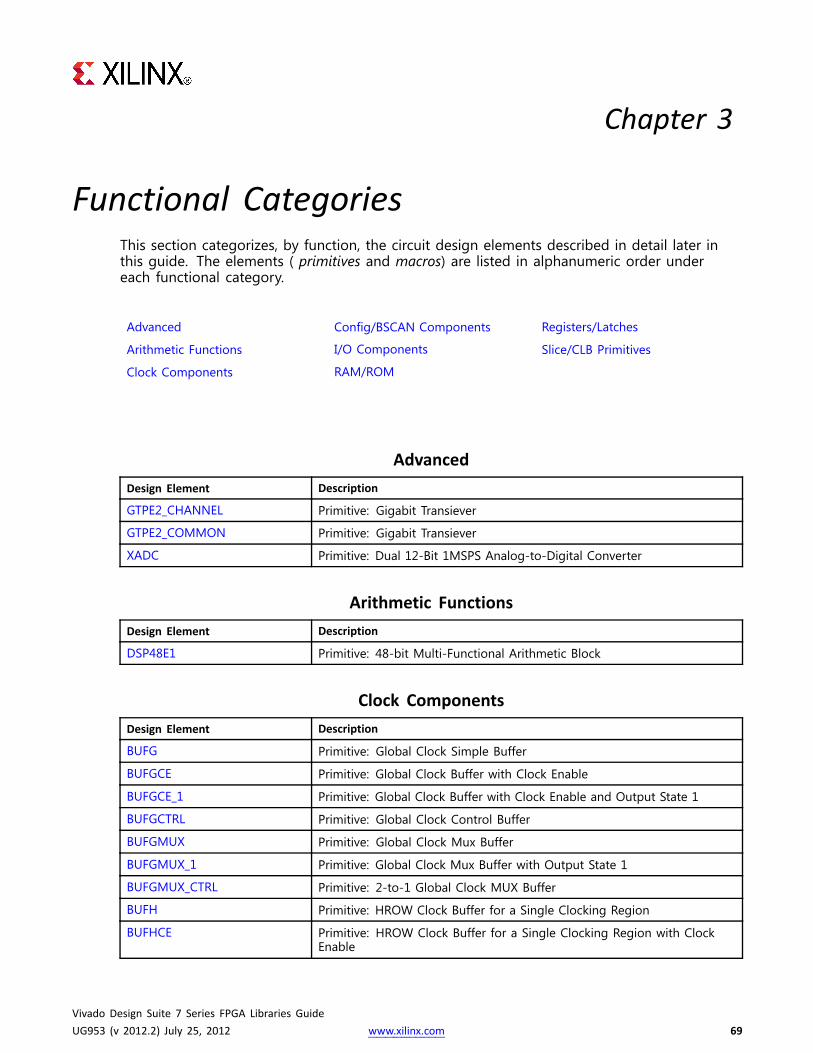
Chapter 3
Functional CategoriesThis section categorizes, by function, the circuit design elements described in detail later inthis guide. The elements ( primitives and macros) are listed in alphanumeric order undereach functional category.
Advanced Config/BSCAN Components Registers/Latches
Arithmetic Functions I/O Components Slice/CLB Primitives
Clock Components RAM/ROM
AdvancedDesign Element Description
GTPE2_CHANNEL Primitive: Gigabit Transiever
GTPE2_COMMON Primitive: Gigabit Transiever
XADC Primitive: Dual 12-Bit 1MSPS Analog-to-Digital Converter
Arithmetic FunctionsDesign Element Description
DSP48E1 Primitive: 48-bit Multi-Functional Arithmetic Block
Clock ComponentsDesign Element Description
BUFG Primitive: Global Clock Simple Buffer
BUFGCE Primitive: Global Clock Buffer with Clock Enable
BUFGCE_1 Primitive: Global Clock Buffer with Clock Enable and Output State 1
BUFGCTRL Primitive: Global Clock Control Buffer
BUFGMUX Primitive: Global Clock Mux Buffer
BUFGMUX_1 Primitive: Global Clock Mux Buffer with Output State 1
BUFGMUX_CTRL Primitive: 2-to-1 Global Clock MUX Buffer
BUFH Primitive: HROW Clock Buffer for a Single Clocking Region
BUFHCE Primitive: HROW Clock Buffer for a Single Clocking Region with ClockEnable
Vivado Design Suite 7 Series FPGA Libraries GuideUG953 (v 2012.2) July 25, 2012 www.xilinx.com 69
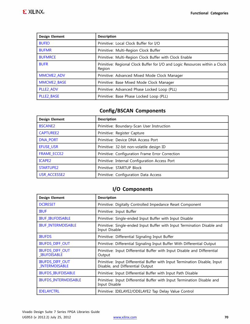
Functional Categories
Design Element Description
BUFIO Primitive: Local Clock Buffer for I/O
BUFMR Primitive: Multi-Region Clock Buffer
BUFMRCE Primitive: Multi-Region Clock Buffer with Clock Enable
BUFR Primitive: Regional Clock Buffer for I/O and Logic Resources within a ClockRegion
MMCME2_ADV Primitive: Advanced Mixed Mode Clock Manager
MMCME2_BASE Primitive: Base Mixed Mode Clock Manager
PLLE2_ADV Primitive: Advanced Phase Locked Loop (PLL)
PLLE2_BASE Primitive: Base Phase Locked Loop (PLL)
Config/BSCAN ComponentsDesign Element Description
BSCANE2 Primitive: Boundary-Scan User Instruction
CAPTUREE2 Primitive: Register Capture
DNA_PORT Primitive: Device DNA Access Port
EFUSE_USR Primitive: 32-bit non-volatile design ID
FRAME_ECCE2 Primitive: Configuration Frame Error Correction
ICAPE2 Primitive: Internal Configuration Access Port
STARTUPE2 Primitive: STARTUP Block
USR_ACCESSE2 Primitive: Configuration Data Access
I/O ComponentsDesign Element Description
DCIRESET Primitive: Digitally Controlled Impedance Reset Component
IBUF Primitive: Input Buffer
IBUF_IBUFDISABLE Primitive: Single-ended Input Buffer with Input Disable
IBUF_INTERMDISABLE Primitive: Single-ended Input Buffer with Input Termination Disable andInput Disable
IBUFDS Primitive: Differential Signaling Input Buffer
IBUFDS_DIFF_OUT Primitive: Differential Signaling Input Buffer With Differential Output
IBUFDS_DIFF_OUT_IBUFDISABLE
Primitive: Input Differential Buffer with Input Disable and DifferentialOutput
IBUFDS_DIFF_OUT_INTERMDISABLE
Primitive: Input Differential Buffer with Input Termination Disable, InputDisable, and Differential Output
IBUFDS_IBUFDISABLE Primitive: Input Differential Buffer with Input Path Disable
IBUFDS_INTERMDISABLE Primitive: Input Differential Buffer with Input Termination Disable andInput Disable
IDELAYCTRL Primitive: IDELAYE2/ODELAYE2 Tap Delay Value Control
Vivado Design Suite 7 Series FPGA Libraries GuideUG953 (v 2012.2) July 25, 2012 www.xilinx.com 70
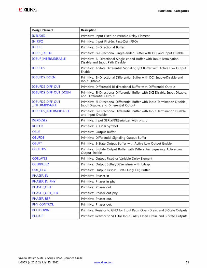
Functional Categories
Design Element Description
IDELAYE2 Primitive: Input Fixed or Variable Delay Element
IN_FIFO Primitive: Input First-In, First-Out (FIFO)
IOBUF Primitive: Bi-Directional Buffer
IOBUF_DCIEN Primitive: Bi-Directional Single-ended Buffer with DCI and Input Disable.
IOBUF_INTERMDISABLE Primitive: Bi-Directional Single-ended Buffer with Input TerminationDisable and Input Path Disable
IOBUFDS Primitive: 3-State Differential Signaling I/O Buffer with Active Low OutputEnable
IOBUFDS_DCIEN Primitive: Bi-Directional Differential Buffer with DCI Enable/Disable andInput Disable
IOBUFDS_DIFF_OUT Primitive: Differential Bi-directional Buffer with Differential Output
IOBUFDS_DIFF_OUT_DCIEN Primitive: Bi-Directional Differential Buffer with DCI Disable, Input Disable,and Differential Output
IOBUFDS_DIFF_OUT_INTERMDISABLE
Primitive: Bi-Directional Differential Buffer with Input Termination Disable,Input Disable, and Differential Output
IOBUFDS_INTERMDISABLE Primitive: Bi-Directional Differential Buffer with Input Termination Disableand Input Disable
ISERDESE2 Primitive: Input SERial/DESerializer with bitslip
KEEPER Primitive: KEEPER Symbol
OBUF Primitive: Output Buffer
OBUFDS Primitive: Differential Signaling Output Buffer
OBUFT Primitive: 3-State Output Buffer with Active Low Output Enable
OBUFTDS Primitive: 3-State Output Buffer with Differential Signaling, Active-LowOutput Enable
ODELAYE2 Primitive: Output Fixed or Variable Delay Element
OSERDESE2 Primitive: Output SERial/DESerializer with bitslip
OUT_FIFO Primitive: Output First-In, First-Out (FIFO) Buffer
PHASER_IN Primitive: Phaser in
PHASER_IN_PHY Primitive: Phaser in phy
PHASER_OUT Primitive: Phaser out.
PHASER_OUT_PHY Primitive: Phaser out phy.
PHASER_REF Primitive: Phaser out.
PHY_CONTROL Primitive: Phaser out.
PULLDOWN Primitive: Resistor to GND for Input Pads, Open-Drain, and 3-State Outputs
PULLUP Primitive: Resistor to VCC for Input PADs, Open-Drain, and 3-State Outputs
Vivado Design Suite 7 Series FPGA Libraries GuideUG953 (v 2012.2) July 25, 2012 www.xilinx.com 71

Functional Categories
RAM/ROM
Design Element Description
FIFO18E1 Primitive: 18Kb FIFO (First-In-First-Out) Block RAM Memory
FIFO36E1 Primitive: 36Kb FIFO (First-In-First-Out) Block RAM Memory
RAM128X1D Primitive: 128-Deep by 1-Wide Dual Port Random Access Memory (SelectRAM)
RAM256X1S Primitive: 256-Deep by 1-Wide Random Access Memory (Select RAM)
RAM32M Primitive: 32-Deep by 8-bit Wide Multi Port Random Access Memory(Select RAM)
RAM32X1D Primitive: 32-Deep by 1-Wide Static Dual Port Synchronous RAM
RAM32X1S Primitive: 32-Deep by 1-Wide Static Synchronous RAM
RAM32X1S_1 Primitive: 32-Deep by 1-Wide Static Synchronous RAM with Negative-EdgeClock
RAM32X2S Primitive: 32-Deep by 2-Wide Static Synchronous RAM
RAM64M Primitive: 64-Deep by 4-bit Wide Multi Port Random Access Memory(Select RAM)
RAM64X1D Primitive: 64-Deep by 1-Wide Dual Port Static Synchronous RAM
RAM64X1S Primitive: 64-Deep by 1-Wide Static Synchronous RAM
RAM64X1S_1 Primitive: 64-Deep by 1-Wide Static Synchronous RAM with Negative-EdgeClock
RAMB18E1 Primitive: 18K-bit Configurable Synchronous Block RAM
RAMB36E1 Primitive: 36K-bit Configurable Synchronous Block RAM
ROM128X1 Primitive: 128-Deep by 1-Wide ROM
ROM256X1 Primitive: 256-Deep by 1-Wide ROM
ROM32X1 Primitive: 32-Deep by 1-Wide ROM
ROM64X1 Primitive: 64-Deep by 1-Wide ROM
Registers/Latches
Design Element Description
FDCE Primitive: D Flip-Flop with Clock Enable and Asynchronous Clear
FDPE Primitive: D Flip-Flop with Clock Enable and Asynchronous Preset
FDRE Primitive: D Flip-Flop with Clock Enable and Synchronous Reset
FDSE Primitive: D Flip-Flop with Clock Enable and Synchronous Set
IDDR Primitive: Input Dual Data-Rate Register
IDDR_2CLK Primitive: Input Dual Data-Rate Register with Dual Clock Inputs
LDCE Primitive: Transparent Data Latch with Asynchronous Clear and Gate Enable
LDPE Primitive: Transparent Data Latch with Asynchronous Preset and GateEnable
ODDR Primitive: Dedicated Dual Data Rate (DDR) Output Register
Vivado Design Suite 7 Series FPGA Libraries GuideUG953 (v 2012.2) July 25, 2012 www.xilinx.com 72
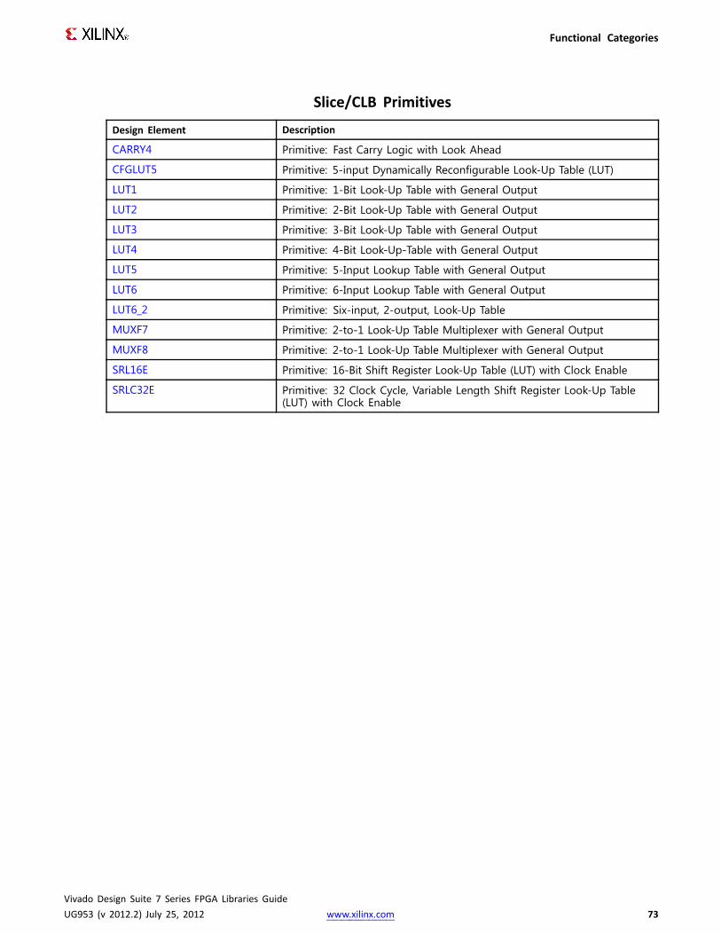
Functional Categories
Slice/CLB Primitives
Design Element Description
CARRY4 Primitive: Fast Carry Logic with Look Ahead
CFGLUT5 Primitive: 5-input Dynamically Reconfigurable Look-Up Table (LUT)
LUT1 Primitive: 1-Bit Look-Up Table with General Output
LUT2 Primitive: 2-Bit Look-Up Table with General Output
LUT3 Primitive: 3-Bit Look-Up Table with General Output
LUT4 Primitive: 4-Bit Look-Up-Table with General Output
LUT5 Primitive: 5-Input Lookup Table with General Output
LUT6 Primitive: 6-Input Lookup Table with General Output
LUT6_2 Primitive: Six-input, 2-output, Look-Up Table
MUXF7 Primitive: 2-to-1 Look-Up Table Multiplexer with General Output
MUXF8 Primitive: 2-to-1 Look-Up Table Multiplexer with General Output
SRL16E Primitive: 16-Bit Shift Register Look-Up Table (LUT) with Clock Enable
SRLC32E Primitive: 32 Clock Cycle, Variable Length Shift Register Look-Up Table(LUT) with Clock Enable
Vivado Design Suite 7 Series FPGA Libraries GuideUG953 (v 2012.2) July 25, 2012 www.xilinx.com 73

Chapter 4
Design Elements
OverviewThis section describes the design elements that can be used with 7 Series architectures. Thedesign elements are organized alphabetically.
The following information is provided for each design element, where applicable:
• Name of element
• Brief description
• Schematic symbol (if any)
• Logic table (if any)
• Port descriptions
• Design Entry Method
• Available attributes (if any)
• Example instantiation code
• For more information
Vivado Design Suite 7 Series FPGA Libraries GuideUG953 (v 2012.2) July 25, 2012 www.xilinx.com 74
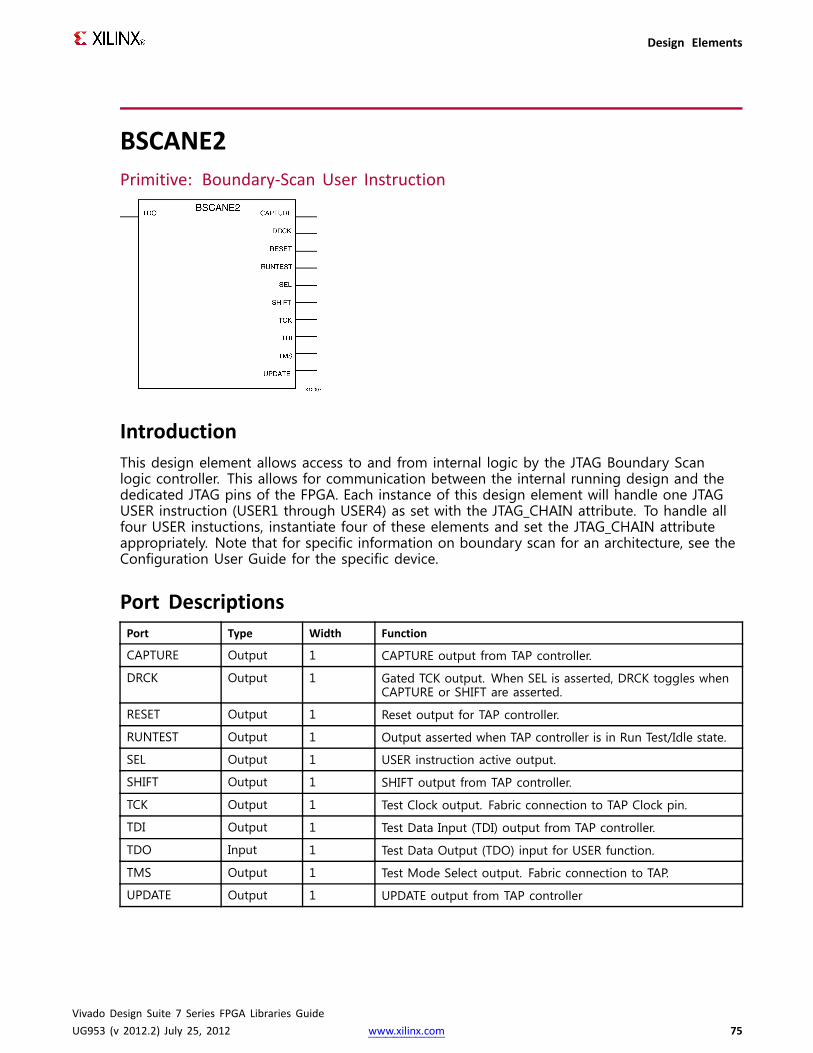
Design Elements
BSCANE2Primitive: Boundary-Scan User Instruction
IntroductionThis design element allows access to and from internal logic by the JTAG Boundary Scanlogic controller. This allows for communication between the internal running design and thededicated JTAG pins of the FPGA. Each instance of this design element will handle one JTAGUSER instruction (USER1 through USER4) as set with the JTAG_CHAIN attribute. To handle allfour USER instuctions, instantiate four of these elements and set the JTAG_CHAIN attributeappropriately. Note that for specific information on boundary scan for an architecture, see theConfiguration User Guide for the specific device.
Port DescriptionsPort Type Width Function
CAPTURE Output 1 CAPTURE output from TAP controller.
DRCK Output 1 Gated TCK output. When SEL is asserted, DRCK toggles whenCAPTURE or SHIFT are asserted.
RESET Output 1 Reset output for TAP controller.
RUNTEST Output 1 Output asserted when TAP controller is in Run Test/Idle state.
SEL Output 1 USER instruction active output.
SHIFT Output 1 SHIFT output from TAP controller.
TCK Output 1 Test Clock output. Fabric connection to TAP Clock pin.
TDI Output 1 Test Data Input (TDI) output from TAP controller.
TDO Input 1 Test Data Output (TDO) input for USER function.
TMS Output 1 Test Mode Select output. Fabric connection to TAP.
UPDATE Output 1 UPDATE output from TAP controller
Vivado Design Suite 7 Series FPGA Libraries GuideUG953 (v 2012.2) July 25, 2012 www.xilinx.com 75

Design Elements
Design Entry MethodInstantiation Recommended
Inference No
CORE Generator™ and wizards No
Macro support No
Available AttributesAttribute Type Allowed Values Default Description
JTAG_CHAIN DECIMAL 1, 2, 3, 4 1 Value for USER command.
VHDL Instantiation TemplateUnless they already exist, copy the following two statements and paste them before the entitydeclaration.Library UNISIM;use UNISIM.vcomponents.all;
-- BSCANE2: Boundary-Scan User Instruction-- 7 Series-- Xilinx HDL Libraries Guide, version 2012.2
BSCANE2_inst : BSCANE2generic map (
JTAG_CHAIN => 1 -- Value for USER command.)port map (
CAPTURE=> CAPTURE, -- 1-bit output: CAPTUREoutput from TAP controller.DRCK=> DRCK, -- 1-bit output: Gated TCK output. When SEL is asserted, DRCK toggles when CAPTUREor
-- SHIFT are asserted.
RESET => RESET, -- 1-bit output: Reset output for TAP controller.RUNTEST=> RUNTEST, -- 1-bit output: Output asserted when TAP controller is in Run Test/Idle state.SEL => SEL, -- 1-bit output: USER instruction active output.SHIFT => SHIFT, -- 1-bit output: SHIFT output from TAP controller.TCK => TCK, -- 1-bit output: Test Clock output. Fabric connection to TAP Clock pin.TDI => TDI, -- 1-bit output: Test Data Input (TDI) output from TAP controller.TMS => TMS, -- 1-bit output: Test Mode Select output. Fabric connection to TAP.UPDATE=> UPDATE, -- 1-bit output: UPDATEoutput from TAP controllerTDO => TDO -- 1-bit input: Test Data Output (TDO) input for USER function.
);
-- End of BSCANE2_inst instantiation
Vivado Design Suite 7 Series FPGA Libraries GuideUG953 (v 2012.2) July 25, 2012 www.xilinx.com 76

Design Elements
Verilog Instantiation Template
// BSCANE2: Boundary-Scan User Instruction// 7 Series// Xilinx HDL Libraries Guide, version 2012.2
BSCANE2#(.JTAG_CHAIN(1) // Value for USER command.
)BSCANE2_inst (
.CAPTURE(CAPTURE), // 1-bit output: CAPTUREoutput from TAP controller.
.DRCK(DRCK), // 1-bit output: Gated TCK output. When SEL is asserted, DRCK toggles when CAPTUREor// SHIFT are asserted.
.RESET(RESET), // 1-bit output: Reset output for TAP controller.
.RUNTEST(RUNTEST), // 1-bit output: Output asserted when TAP controller is in Run Test/Idle state.
.SEL(SEL), // 1-bit output: USER instruction active output.
.SHIFT(SHIFT), // 1-bit output: SHIFT output from TAP controller.
.TCK(TCK), // 1-bit output: Test Clock output. Fabric connection to TAP Clock pin.
.TDI(TDI), // 1-bit output: Test Data Input (TDI) output from TAP controller.
.TMS(TMS), // 1-bit output: Test Mode Select output. Fabric connection to TAP.
.UPDATE(UPDATE), // 1-bit output: UPDATEoutput from TAP controller
.TDO(TDO) // 1-bit input: Test Data Output (TDO) input for USER function.);
// End of BSCANE2_inst instantiation
For More InformationSee the 7 series FPGA User Documentation (User Guides and Data Sheets).
Vivado Design Suite 7 Series FPGA Libraries GuideUG953 (v 2012.2) July 25, 2012 www.xilinx.com 77

Design Elements
BUFGPrimitive: Global Clock Simple Buffer
IntroductionThis design element is a high-fanout buffer that connects signals to the global routingresources for low skew distribution of the signal. BUFGs are typically used on clock nets aswell other high fanout nets like sets/resets and clock enables.
Port DescriptionsPort Type Width Function
I Input 1 Clock input
O Output 1 Clock output
Design Entry MethodInstantiation Yes
Inference Recommended
CORE Generator™ and wizards No
Macro support No
VHDL Instantiation TemplateUnless they already exist, copy the following two statements and paste them before the entitydeclaration.Library UNISIM;use UNISIM.vcomponents.all;
-- BUFG: Global Clock Simple Buffer-- 7 Series-- Xilinx HDL Libraries Guide, version 2012.2
BUFG_inst : BUFGport map (
O => O, -- 1-bit output: Clock outputI => I -- 1-bit input: Clock input
);
-- End of BUFG_inst instantiation
Vivado Design Suite 7 Series FPGA Libraries GuideUG953 (v 2012.2) July 25, 2012 www.xilinx.com 78

Design Elements
Verilog Instantiation Template
// BUFG: Global Clock Simple Buffer// 7 Series// Xilinx HDL Libraries Guide, version 2012.2
BUFG BUFG_inst (.O(O), // 1-bit output: Clock output.I(I) // 1-bit input: Clock input
);
// End of BUFG_inst instantiation
For More InformationSee the 7 series FPGA User Documentation (User Guides and Data Sheets).
Vivado Design Suite 7 Series FPGA Libraries GuideUG953 (v 2012.2) July 25, 2012 www.xilinx.com 79

Design Elements
BUFGCEPrimitive: Global Clock Buffer with Clock Enable
IntroductionThis design element is a global clock buffer with a single gated input. Its O output is "0" whenclock enable (CE) is Low (inactive). When clock enable (CE) is High, the I input is transferred tothe O output.
Logic TableInputs Outputs
I CE O
X 0 0
I 1 I
Design Entry MethodInstantiation Recommended
Inference No
CORE Generator™ and wizards No
Macro support No
VHDL Instantiation TemplateUnless they already exist, copy the following two statements and paste them before the entitydeclaration.Library UNISIM;use UNISIM.vcomponents.all;
-- BUFGCE: Global Clock Buffer with Clock Enable-- 7 Series-- Xilinx HDL Libraries Guide, version 2012.2
BUFGCE_inst : BUFGCEport map (
O => O, -- 1-bit output: Clock outputCE => CE, -- 1-bit input: Clock enable input for I0I => I -- 1-bit input: Primary clock
);
-- End of BUFGCE_inst instantiation
Vivado Design Suite 7 Series FPGA Libraries GuideUG953 (v 2012.2) July 25, 2012 www.xilinx.com 80

Design Elements
Verilog Instantiation Template
// BUFGCE: Global Clock Buffer with Clock Enable// 7 Series// Xilinx HDL Libraries Guide, version 2012.2
BUFGCEBUFGCE_inst (.O(O), // 1-bit output: Clock output.CE(CE), // 1-bit input: Clock enable input for I0.I(I) // 1-bit input: Primary clock
);
// End of BUFGCE_inst instantiation
For More InformationSee the 7 series FPGA User Documentation (User Guides and Data Sheets).
Vivado Design Suite 7 Series FPGA Libraries GuideUG953 (v 2012.2) July 25, 2012 www.xilinx.com 81
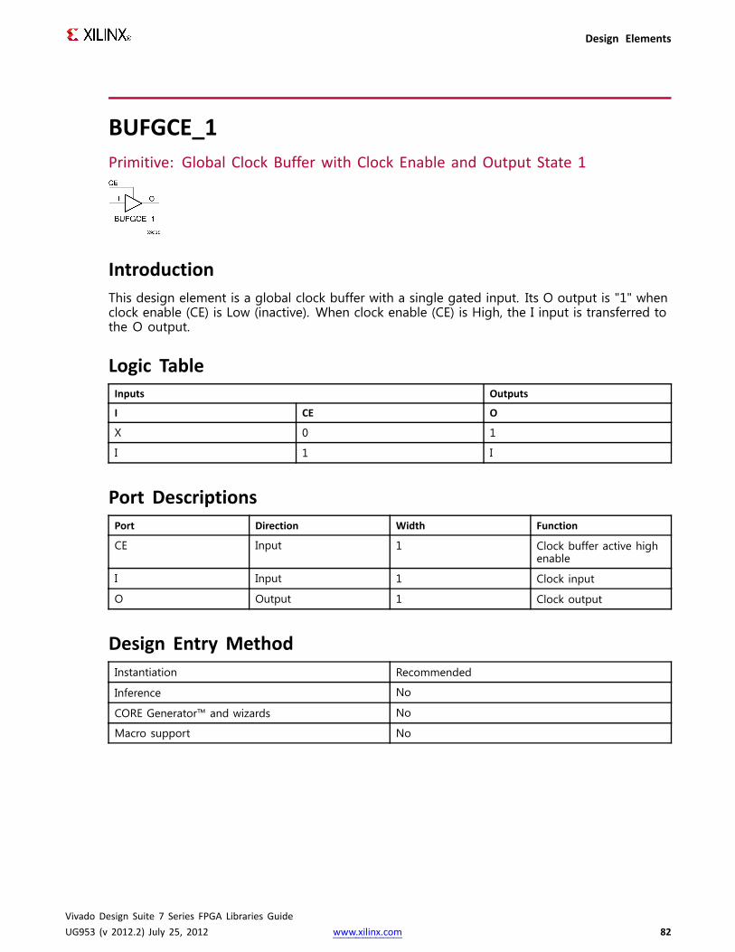
Design Elements
BUFGCE_1Primitive: Global Clock Buffer with Clock Enable and Output State 1
IntroductionThis design element is a global clock buffer with a single gated input. Its O output is "1" whenclock enable (CE) is Low (inactive). When clock enable (CE) is High, the I input is transferred tothe O output.
Logic TableInputs Outputs
I CE O
X 0 1
I 1 I
Port DescriptionsPort Direction Width Function
CE Input 1 Clock buffer active highenable
I Input 1 Clock input
O Output 1 Clock output
Design Entry MethodInstantiation Recommended
Inference No
CORE Generator™ and wizards No
Macro support No
Vivado Design Suite 7 Series FPGA Libraries GuideUG953 (v 2012.2) July 25, 2012 www.xilinx.com 82
Design Elements
VHDL Instantiation TemplateUnless they already exist, copy the following two statements and paste them before the entitydeclaration.Library UNISIM;use UNISIM.vcomponents.all;
-- BUFGCE_1: Global Clock Buffer with Clock Enable and Output State 1-- 7 Series-- Xilinx HDL Libraries Guide, version 2012.2
BUFGCE_1_inst : BUFGCE_1port map (
O => O, -- 1-bit output: Clock outputCE => CE, -- 1-bit input: Clock enable input for I0I => I -- 1-bit input: Primary clock
);
-- End of BUFGCE_1_inst instantiation
Verilog Instantiation Template
// BUFGCE_1: Global Clock Buffer with Clock Enable and Output State 1// 7 Series// Xilinx HDL Libraries Guide, version 2012.2
BUFGCE_1BUFGCE_1_inst (.O(O), // 1-bit output: Clock output.CE(CE), // 1-bit input: Clock enable input for I0.I(I) // 1-bit input: Primary clock
);
// End of BUFGCE_1_inst instantiation
For More InformationSee the 7 series FPGA User Documentation (User Guides and Data Sheets).
Vivado Design Suite 7 Series FPGA Libraries GuideUG953 (v 2012.2) July 25, 2012 www.xilinx.com 83

Design Elements
BUFGCTRLPrimitive: Global Clock Control Buffer
IntroductionBUFGCTRL primitive is a 7 series global clock buffer that is designed as asynchronous/asynchronous "glitch free" 2:1 multiplexer with two clock inputs. Unlike globalclock buffers that are found in previous generations of FPGAs, these clock buffers are designedwith more control pins to provide a wider range of functionality and more robust inputswitching. BUFGCTRL is not limited to clocking applications.
Port DescriptionsPort Type Width Function
CE0 Input 1 Clock enable input for the I0 clock input. A setup/hold timemust be guarenteed when you are using the CE0 pin toenable this input. Failure to meet this requirement couldresult in a clock glitch.
CE1 Input 1 Clock enable input for the I1 clock input. A setup/hold timemust be guarenteed when you are using the CE1 pin toenable this input. Failure to meet this requirement couldresult in a clock glitch.
IGNORE0 Input 1 Clock ignore input for I0 input. Asserting the IGNORE pinwill bypass the BUFGCTRL from detecting the conditionsfor switching between two clock inputs. In other words,asserting IGNORE causes the MUX to switch the inputs atthe instant the select pin changes. IGNORE0 causes theoutput to switch away from the I0 input immediately whenthe select pin changes, while IGNORE1 causes the output toswitch away from the I1 input immediately when the selectpin changes.
IGNORE1 Input 1 Clock ignore input for I1 input. Asserting the IGNORE pinwill bypass the BUFGCTRL from detecting the conditionsfor switching between two clock inputs. In other words,asserting IGNORE causes the MUX to switch the inputs atthe instant the select pin changes. IGNORE0 causes theoutput to switch away from the I0 input immediately whenthe select pin changes, while IGNORE1 causes the output to
Vivado Design Suite 7 Series FPGA Libraries GuideUG953 (v 2012.2) July 25, 2012 www.xilinx.com 84

Design Elements
Port Type Width Functionswitch away from the I1 input immediately when the selectpin changes.
I0 Input 1 Primary clock input into the BUFGCTRL enabled by the CE0input and selected by the S0 input.
I1 Input 1 Secondary clock input into the BUFGCTRL enabled by theCE1 input and selected by the S1 input.
O Output 1 Clock output
S0 Input 1 Clock select input for I0. The S pins represent the clockselect pin for each clock input. When using the S pin asinput select, there is a setup/hold time requirement. UnlikeCE pins, failure to meet this requirement will not result ina clock glitch. However, it can cause the output clock toappear one clock cycle later.
S1 Input 1 Clock select input for I1. The S pins represent the clockselect pin for each clock input. When using the S pin asinput select, there is a setup/hold time requirement. UnlikeCE pins, failure to meet this requirement will not result ina clock glitch. However, it can cause the output clock toappear one clock cycle later.
Design Entry MethodInstantiation Recommended
Inference No
CORE Generator™ and wizards No
Macro support No
Available AttributesAttribute Type Allowed Values Default Description
INIT_OUT DECIMAL 0, 1 0 Initializes the BUFGCTRL output to thespecified value after configuration.
PRESELECT_I0 BOOLEAN FALSE, TRUE FALSE If TRUE, BUFGCTRL output uses I0 input afterconfiguration.
PRESELECT_I1 BOOLEAN FALSE, TRUE FALSE If TRUE, BUFGCTRL output uses I1 input afterconfiguration.
Note Both PRESELECT attributes might not be TRUE at the same time.
Vivado Design Suite 7 Series FPGA Libraries GuideUG953 (v 2012.2) July 25, 2012 www.xilinx.com 85
Design Elements
VHDL Instantiation TemplateUnless they already exist, copy the following two statements and paste them before the entitydeclaration.Library UNISIM;use UNISIM.vcomponents.all;
-- BUFGCTRL: Global Clock Control Buffer-- 7 Series-- Xilinx HDL Libraries Guide, version 2012.2
BUFGCTRL_inst : BUFGCTRLgeneric map (
INIT_OUT => 0, -- Initial value of BUFGCTRLoutput ($VALUES;)PRESELECT_I0 => FALSE, -- BUFGCTRLoutput uses I0 input ($VALUES;)PRESELECT_I1 => FALSE -- BUFGCTRLoutput uses I1 input ($VALUES;)
)port map (
O => O, -- 1-bit output: Clock outputCE0 => CE0, -- 1-bit input: Clock enable input for I0CE1 => CE1, -- 1-bit input: Clock enable input for I1I0 => I0, -- 1-bit input: Primary clockI1 => I1, -- 1-bit input: Secondary clockIGNORE0 => IGNORE0, -- 1-bit input: Clock ignore input for I0IGNORE1 => IGNORE1, -- 1-bit input: Clock ignore input for I1S0 => S0, -- 1-bit input: Clock select for I0S1 => S1 -- 1-bit input: Clock select for I1
);
-- End of BUFGCTRL_inst instantiation
Verilog Instantiation Template
// BUFGCTRL: Global Clock Control Buffer// 7 Series// Xilinx HDL Libraries Guide, version 2012.2
BUFGCTRL#(.INIT_OUT(0), // Initial value of BUFGCTRLoutput ($VALUES;).PRESELECT_I0("FALSE"), // BUFGCTRLoutput uses I0 input ($VALUES;).PRESELECT_I1("FALSE") // BUFGCTRLoutput uses I1 input ($VALUES;)
)BUFGCTRL_inst (
.O(O), // 1-bit output: Clock output
.CE0(CE0), // 1-bit input: Clock enable input for I0
.CE1(CE1), // 1-bit input: Clock enable input for I1
.I0(I0), // 1-bit input: Primary clock
.I1(I1), // 1-bit input: Secondary clock
.IGNORE0(IGNORE0), // 1-bit input: Clock ignore input for I0
.IGNORE1(IGNORE1), // 1-bit input: Clock ignore input for I1
.S0(S0), // 1-bit input: Clock select for I0
.S1(S1) // 1-bit input: Clock select for I1);
// End of BUFGCTRL_inst instantiation
For More InformationSee the 7 series FPGA User Documentation (User Guides and Data Sheets).
Vivado Design Suite 7 Series FPGA Libraries GuideUG953 (v 2012.2) July 25, 2012 www.xilinx.com 86

Design Elements
BUFGMUXPrimitive: Global Clock Mux Buffer
IntroductionThis design element is a global clock buffer, based off of the BUFGCTRL, that can selectbetweeen two input clocks: I0 and I1. When the select input (S) is Low, the signal on I0 isselected for output (O). When the select input (S) is High, the signal on I1 is selected for output.BUFGMUX BUFGMUX_1 are distinguished by the state the output assumes when that outputswitches between clocks in response to a change in its select input. BUFGMUX assumes outputstate 0 and BUFGMUX_1 assumes output state 1.
Logic TableInputs Outputs
I0 I1 S O
I0 X 0 I0
X I1 1 I1
X X ↑ 0
X X ↓ 0
Port DescriptionsPort Direction Width Function
I0 Input 1 Clock buffer input. Thisinput is reflected on theoutput O when the Sinput is zero.
I1 Input 1 Clock buffer input. Thisinput is reflected on theoutput O when the Sinput is one.
O Output 1 Clock buffer output.
S Input 1 Clock buffer select input.When low, selects I0input and when high, theI1 input is slected
Vivado Design Suite 7 Series FPGA Libraries GuideUG953 (v 2012.2) July 25, 2012 www.xilinx.com 87

Design Elements
Design Entry MethodInstantiation Recommended
Inference No
CORE Generator™ and wizards No
Macro support No
VHDL Instantiation TemplateUnless they already exist, copy the following two statements and paste them before the entitydeclaration.Library UNISIM;use UNISIM.vcomponents.all;
-- BUFGMUX:Global Clock Mux Buffer-- 7 Series-- Xilinx HDL Libraries Guide, version 2012.2
BUFGMUX_inst : BUFGMUXport map (
O => O, -- 1-bit output: Clock outputI0 => I0, -- 1-bit input: Clock input (S=0)I1 => I1, -- 1-bit input: Clock input (S=1)S => S -- 1-bit input: Clock select
);
-- End of BUFGMUX_inst instantiation
Verilog Instantiation Template
// BUFGMUX:Global Clock Mux Buffer// 7 Series// Xilinx HDL Libraries Guide, version 2012.2
BUFGMUX#()BUFGMUX_inst (
.O(O), // 1-bit output: Clock output
.I0(I0), // 1-bit input: Clock input (S=0)
.I1(I1), // 1-bit input: Clock input (S=1)
.S(S) // 1-bit input: Clock select);
// End of BUFGMUX_inst instantiation
For More InformationSee the 7 series FPGA User Documentation (User Guides and Data Sheets).
Vivado Design Suite 7 Series FPGA Libraries GuideUG953 (v 2012.2) July 25, 2012 www.xilinx.com 88
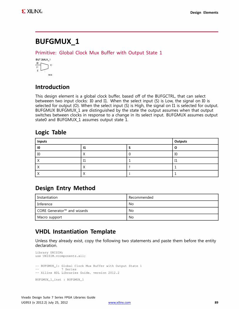
Design Elements
BUFGMUX_1Primitive: Global Clock Mux Buffer with Output State 1
IntroductionThis design element is a global clock buffer, based off of the BUFGCTRL, that can selectbetweeen two input clocks: I0 and I1. When the select input (S) is Low, the signal on I0 isselected for output (O). When the select input (S) is High, the signal on I1 is selected for output.BUFGMUX BUFGMUX_1 are distinguished by the state the output assumes when that outputswitches between clocks in response to a change in its select input. BUFGMUX assumes outputstate0 and BUFGMUX_1 assumes output state 1.
Logic TableInputs Outputs
I0 I1 S O
I0 X 0 I0
X I1 1 I1
X X ↑ 1
X X ↓ 1
Design Entry MethodInstantiation Recommended
Inference No
CORE Generator™ and wizards No
Macro support No
VHDL Instantiation TemplateUnless they already exist, copy the following two statements and paste them before the entitydeclaration.Library UNISIM;use UNISIM.vcomponents.all;
-- BUFGMUX_1: Global Clock Mux Buffer with Output State 1-- 7 Series-- Xilinx HDL Libraries Guide, version 2012.2
BUFGMUX_1_inst : BUFGMUX_1
Vivado Design Suite 7 Series FPGA Libraries GuideUG953 (v 2012.2) July 25, 2012 www.xilinx.com 89
Design Elements
port map (O => O, -- 1-bit output: Clock outputI0 => I0, -- 1-bit input: Clock input (S=0)I1 => I1, -- 1-bit input: Clock input (S=1)S => S -- 1-bit input: Clock select
);
-- End of BUFGMUX_1_inst instantiation
Verilog Instantiation Template
// BUFGMUX_1: Global Clock Mux Buffer with Output State 1// 7 Series// Xilinx HDL Libraries Guide, version 2012.2
BUFGMUX_1#()BUFGMUX_1_inst (
.O(O), // 1-bit output: Clock output
.I0(I0), // 1-bit input: Clock input (S=0)
.I1(I1), // 1-bit input: Clock input (S=1)
.S(S) // 1-bit input: Clock select);
// End of BUFGMUX_1_inst instantiation
For More InformationSee the 7 series FPGA User Documentation (User Guides and Data Sheets).
Vivado Design Suite 7 Series FPGA Libraries GuideUG953 (v 2012.2) July 25, 2012 www.xilinx.com 90
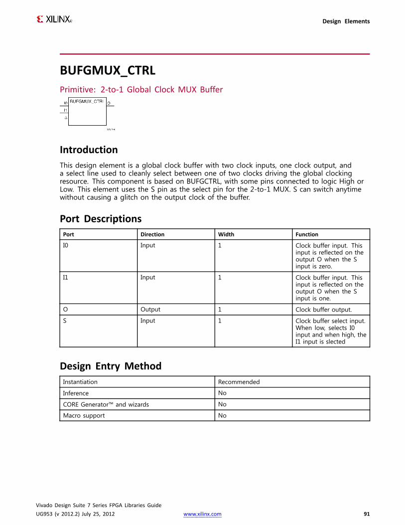
Design Elements
BUFGMUX_CTRLPrimitive: 2-to-1 Global Clock MUX Buffer
IntroductionThis design element is a global clock buffer with two clock inputs, one clock output, anda select line used to cleanly select between one of two clocks driving the global clockingresource. This component is based on BUFGCTRL, with some pins connected to logic High orLow. This element uses the S pin as the select pin for the 2-to-1 MUX. S can switch anytimewithout causing a glitch on the output clock of the buffer.
Port DescriptionsPort Direction Width Function
I0 Input 1 Clock buffer input. Thisinput is reflected on theoutput O when the Sinput is zero.
I1 Input 1 Clock buffer input. Thisinput is reflected on theoutput O when the Sinput is one.
O Output 1 Clock buffer output.
S Input 1 Clock buffer select input.When low, selects I0input and when high, theI1 input is slected
Design Entry MethodInstantiation Recommended
Inference No
CORE Generator™ and wizards No
Macro support No
Vivado Design Suite 7 Series FPGA Libraries GuideUG953 (v 2012.2) July 25, 2012 www.xilinx.com 91

Design Elements
VHDL Instantiation TemplateUnless they already exist, copy the following two statements and paste them before the entitydeclaration.Library UNISIM;use UNISIM.vcomponents.all;
-- BUFGMUX_CTRL:2-to-1 Global Clock MUXBuffer-- 7 Series-- Xilinx HDL Libraries Guide, version 2012.2
BUFGMUX_CTRL_inst : BUFGMUX_CTRLport map (
O => O, -- 1-bit output: Clock outputI0 => I0, -- 1-bit input: Clock input (S=0)I1 => I1, -- 1-bit input: Clock input (S=1)S => S -- 1-bit input: Clock select
);
-- End of BUFGMUX_CTRL_inst instantiation
Verilog Instantiation Template
// BUFGMUX_CTRL:2-to-1 Global Clock MUXBuffer// 7 Series// Xilinx HDL Libraries Guide, version 2012.2
BUFGMUX_CTRLBUFGMUX_CTRL_inst (.O(O), // 1-bit output: Clock output.I0(I0), // 1-bit input: Clock input (S=0).I1(I1), // 1-bit input: Clock input (S=1).S(S) // 1-bit input: Clock select
);
// End of BUFGMUX_CTRL_inst instantiation
For More InformationSee the 7 series FPGA User Documentation (User Guides and Data Sheets).
Vivado Design Suite 7 Series FPGA Libraries GuideUG953 (v 2012.2) July 25, 2012 www.xilinx.com 92

Design Elements
BUFHPrimitive: HROW Clock Buffer for a Single Clocking Region
IntroductionThe BUFH primitive allows direct access to the clock region entry point of the global buffer(BUFG) resource. This allows access to unused portions of the global clocking network to beused as high-speed, low skew local (single clock region) routing resources. Please refer to the 7series FPGA Clocking Resources User Guide for details for using this component.
Port DescriptionsPort Type Width Function
I Input 1 Clock input
O Output 1 Clock output
Design Entry MethodInstantiation Yes
Inference No
CORE Generator™ and wizards No
Macro support No
For More InformationSee the 7 series FPGA User Documentation (User Guides and Data Sheets).
Vivado Design Suite 7 Series FPGA Libraries GuideUG953 (v 2012.2) July 25, 2012 www.xilinx.com 93

Design Elements
BUFHCEPrimitive: HROW Clock Buffer for a Single Clocking Region with Clock Enable
IntroductionThe BUFHCE primitive allows direct access to the clock region entry point of the global buffer(BUFG) resource. This allows access to unused portions of the global clocking network to beused as high-speed, low skew local (single clock region) routing resources. Addtionaly, the CEor clock enable input allows for finer-grained control of clock enabling or gating to allow forpower reduction for circuitry or portions of the design not constantly used. Please refer to the7 series FPGA Clocking Resources User Guide for details for using this component.
Port DescriptionsPort Type Width Function
CE Input 1 Enables propagation of signal from I to O. When low,performs a glitchless transition of the output to INIT_OUTvalue.
I Input 1 Clock input
O Output 1 Clock output
Design Entry MethodInstantiation Yes
Inference No
CORE Generator™ and wizards No
Macro support No
Available AttributesAttribute Type Allowed Values Default Description
CE_TYPE STRING "SYNC","ASYNC"
"SYNC" Sets clock enable behavior where "SYNC"allows for a glitchless transition to and fromthe INIT_OUT value. "ASYNC" is generally usedto create a more immediate transition such aswhen you can expect the clock to be stoppedor when using the BUFHCE for a high fanoutcontrol or data path routing instead of a clockbuffer.
Vivado Design Suite 7 Series FPGA Libraries GuideUG953 (v 2012.2) July 25, 2012 www.xilinx.com 94

Design Elements
Attribute Type Allowed Values Default Description
INIT_OUT DECIMAL 0, 1 0 Initial output value, also indicates stop low vsstop high behavior
VHDL Instantiation TemplateUnless they already exist, copy the following two statements and paste them before the entitydeclaration.Library UNISIM;use UNISIM.vcomponents.all;
-- BUFHCE: HROWClock Buffer for a Single Clocking Region with Clock Enable-- 7 Series-- Xilinx HDL Libraries Guide, version 2012.2
BUFHCE_inst : BUFHCEgeneric map (
CE_TYPE => "SYNC", -- "SYNC" (glitchless switching) or "ASYNC" (immediate switch)INIT_OUT => 0 -- Initial output value (0-1)
)port map (
O => O, -- 1-bit output: Clock outputCE => CE, -- 1-bit input: Active high enableI => I -- 1-bit input: Clock input
);
-- End of BUFHCE_inst instantiation
Verilog Instantiation Template
// BUFHCE: HROWClock Buffer for a Single Clocking Region with Clock Enable// 7 Series// Xilinx HDL Libraries Guide, version 2012.2
BUFHCE#(.CE_TYPE("SYNC"), // "SYNC" (glitchless switching) or "ASYNC" (immediate switch).INIT_OUT(0) // Initial output value (0-1)
)BUFHCE_inst (
.O(O), // 1-bit output: Clock output
.CE(CE), // 1-bit input: Active high enable
.I(I) // 1-bit input: Clock input);
// End of BUFHCE_inst instantiation
For More InformationSee the 7 series FPGA User Documentation (User Guides and Data Sheets).
Vivado Design Suite 7 Series FPGA Libraries GuideUG953 (v 2012.2) July 25, 2012 www.xilinx.com 95

Design Elements
BUFIOPrimitive: Local Clock Buffer for I/O
IntroductionThis design element is simply a clock-in, clock-out buffer. It drives a dedicated clock net withinthe I/O column, independent of the global clock resources. Thus, these elements are ideallysuited for source-synchronous data capture (forwarded/receiver clock distribution). They canbe driven by a dedicated MRCC I/O located in the same clock region or a BUFMRCE/BUFMRcomponent capable of clocking multiple clock regions. The BUFIO can only drive I/Ocomponents within the bank in which they exist. These elements cannot directly drive logicresources (CLB, block RAM, etc.) because the I/O clock network only reaches the I/O column.
Port DescriptionsPort Type Width Function
I Input 1 Input port to clock buffer. Connectthis to an IBUFG connected to atop-level port or an associatedBUFMR buffer.
O Output 1 Output port from clock buffer.Connect this to the clock inputs tosynchronous I/O components like theISERDESE2, OSERDESE2, IDDR, ODDRor register connected directly to anI/O port (inferred or instantiated).
Design Entry MethodInstantiation Yes
Inference No
CORE Generator™ and wizards No
Macro support No
Vivado Design Suite 7 Series FPGA Libraries GuideUG953 (v 2012.2) July 25, 2012 www.xilinx.com 96
Design Elements
VHDL Instantiation TemplateUnless they already exist, copy the following two statements and paste them before the entitydeclaration.Library UNISIM;use UNISIM.vcomponents.all;
-- BUFIO: Local Clock Buffer for I/O-- 7 Series-- Xilinx HDL Libraries Guide, version 2012.2
BUFIO_inst : BUFIOport map (
O => O, -- 1-bit output: Clock output (connect to I/O clock loads).I => I -- 1-bit input: Clock input (connect to an IBUFG or BUFMR).
);
-- End of BUFIO_inst instantiation
Verilog Instantiation Template
// BUFIO: Local Clock Buffer for I/O// 7 Series// Xilinx HDL Libraries Guide, version 2012.2
BUFIO BUFIO_inst (.O(O), // 1-bit output: Clock output (connect to I/O clock loads)..I(I) // 1-bit input: Clock input (connect to an IBUFG or BUFMR).
);
// End of BUFIO_inst instantiation
For More InformationSee the 7 series FPGA User Documentation (User Guides and Data Sheets).
Vivado Design Suite 7 Series FPGA Libraries GuideUG953 (v 2012.2) July 25, 2012 www.xilinx.com 97

Design Elements
BUFMRPrimitive: Multi-Region Clock Buffer
IntroductionThe BUFMR is a simple clock-in/clock-out buffer. The BUFMR replaces the multi-region/banksupport of the BUFR and BUFIO available in prior Virtex architectures. There are two BUFMRs inevery bank and each buffer can be driven by one specific MRCC in the same bank. The BUFMRsdrive the BUFIOs and/or BUFRs in the same region/banks and in the region above and belowvia the I/O clocking backbone. It is not suggested to use a BUFMR when driving BUFRs usingclock dividers (not in bypass) and instead use a BUFMRCE component.
Port DescriptionsPort Direction Width Function
I Input 1 BUFMR clock input pin. Connect to an IBUFG input that in turnis directly connected to a MRCC I/O port.
O Output 1 BUFMR clock output pin. Connect to BUFIOs and/or BUFRs tobe driven in adjacent regions.
Design Entry MethodInstantiation Yes
Inference No
CORE Generator™ and wizards No
Macro support No
VHDL Instantiation TemplateUnless they already exist, copy the following two statements and paste them before the entitydeclaration.Library UNISIM;use UNISIM.vcomponents.all;
-- BUFMR: Multi-Region Clock Buffer-- 7 Series-- Xilinx HDL Libraries Guide, version 2012.2
BUFMR_inst : BUFMRport map (
O => O, -- 1-bit output: Clock output (connect to BUFIOs/BUFRs)I => I -- 1-bit input: Clock input (Connect to IBUFG)
);
Vivado Design Suite 7 Series FPGA Libraries GuideUG953 (v 2012.2) July 25, 2012 www.xilinx.com 98

Design Elements
-- End of BUFMR_inst instantiation
Verilog Instantiation Template
// BUFMR: Multi-Region Clock Buffer// 7 Series// Xilinx HDL Libraries Guide, version 2012.2
BUFMRBUFMR_inst (.O(O), // 1-bit output: Clock output (connect to BUFIOs/BUFRs).I(I) // 1-bit input: Clock input (Connect to IBUFG)
);
// End of BUFMR_inst instantiation
For More InformationSee the 7 series FPGA User Documentation (User Guides and Data Sheets).
Vivado Design Suite 7 Series FPGA Libraries GuideUG953 (v 2012.2) July 25, 2012 www.xilinx.com 99

Design Elements
BUFMRCEPrimitive: Multi-Region Clock Buffer with Clock Enable
IntroductionThe BUFMRCE is a simple clock-in/clock-out buffer with clock with clock enable (CE).Asserting CE stops the output clock to a user specified value. The BUFMRCE replaces themulti-region/bank support of the BUFR and BUFIO available in prior Virtex architectures. Thereare two BUFMRCEs in every bank and each buffer can be driven by one specific MRCC in thesame bank. The BUFMRCE drives the BUFIOs and/or BUFRs in the same region/banks and inthe region above and below via the I/O clocking backbone. When using BUFR dividers (not inbypass), the BUFMRCE must be disabled by deasserting the CE pin, the BUFR must be reset(cleared by asserting CLR), and then the CE signal should be asserted. This sequence ensuresthat all BUFR output clocks are phase aligned. If the dividers within the BUFRs are not used,then this additional circuitry is not necessary. If the clock enable circuitry is not needed, aBUFMR component should be used in place of a BUFMRCE.
Port DescriptionsPort Type Width Function
CE Input 1 Active high buffer enable input. When low, output will settleto INIT_OUT value.
I Input 1 BUFMR clock input pin. Connect to an IBUFG input that in turnis directly connected to a MRCC I/O port.
O Output 1 BUFMR clock output pin. Connect to BUFIOs and/or BUFRs tobe driven in the same and adjacent regions.
Design Entry MethodInstantiation Yes
Inference No
CORE Generator™ and wizards No
Macro support No
Vivado Design Suite 7 Series FPGA Libraries GuideUG953 (v 2012.2) July 25, 2012 www.xilinx.com 100
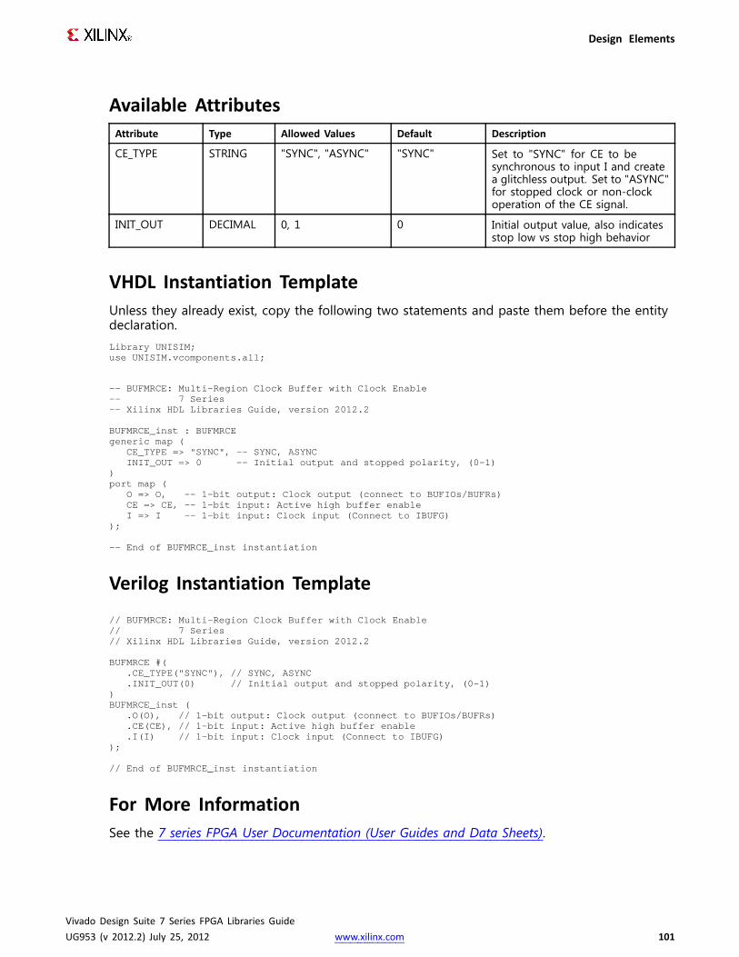
Design Elements
Available AttributesAttribute Type Allowed Values Default Description
CE_TYPE STRING "SYNC", "ASYNC" "SYNC" Set to "SYNC" for CE to besynchronous to input I and createa glitchless output. Set to "ASYNC"for stopped clock or non-clockoperation of the CE signal.
INIT_OUT DECIMAL 0, 1 0 Initial output value, also indicatesstop low vs stop high behavior
VHDL Instantiation TemplateUnless they already exist, copy the following two statements and paste them before the entitydeclaration.Library UNISIM;use UNISIM.vcomponents.all;
-- BUFMRCE:Multi-Region Clock Buffer with Clock Enable-- 7 Series-- Xilinx HDL Libraries Guide, version 2012.2
BUFMRCE_inst : BUFMRCEgeneric map (
CE_TYPE => "SYNC", -- SYNC, ASYNCINIT_OUT => 0 -- Initial output and stopped polarity, (0-1)
)port map (
O => O, -- 1-bit output: Clock output (connect to BUFIOs/BUFRs)CE => CE, -- 1-bit input: Active high buffer enableI => I -- 1-bit input: Clock input (Connect to IBUFG)
);
-- End of BUFMRCE_inst instantiation
Verilog Instantiation Template
// BUFMRCE:Multi-Region Clock Buffer with Clock Enable// 7 Series// Xilinx HDL Libraries Guide, version 2012.2
BUFMRCE#(.CE_TYPE("SYNC"), // SYNC, ASYNC.INIT_OUT(0) // Initial output and stopped polarity, (0-1)
)BUFMRCE_inst (
.O(O), // 1-bit output: Clock output (connect to BUFIOs/BUFRs)
.CE(CE), // 1-bit input: Active high buffer enable
.I(I) // 1-bit input: Clock input (Connect to IBUFG));
// End of BUFMRCE_inst instantiation
For More InformationSee the 7 series FPGA User Documentation (User Guides and Data Sheets).
Vivado Design Suite 7 Series FPGA Libraries GuideUG953 (v 2012.2) July 25, 2012 www.xilinx.com 101

Design Elements
BUFRPrimitive: Regional Clock Buffer for I/O and Logic Resources within a ClockRegion
IntroductionThe BUFR is a regional clock buffer available in 7 series devices. BUFRs drive clock signals to adedicated clock net within a clock region, independent from the global clock tree. Each BUFRcan drive the regional clock nets in the region in which it is located. Unlike BUFIOs, BUFRs candrive the I/O logic and logic resources (CLB, block RAM, etc.) in the existing clock region. BUFRscan be driven by either the output from an IBUFG, BUFMRCE, MMCM or local interconnect. Inaddition, BUFRs are capable of generating divided clock outputs with respect to the clock input.The divide value is an integer between one and eight. BUFRs are ideal for source-synchronousapplications requiring clock domain crossing or serial-to-parallel conversion. There are twoBUFRs in a typical clock region (two regional clock networks). If local clocking is needed inmultiple clock regions, the BUFMRCE can drive multiple BUFRs in adjacent clock regions tofurther extend this clocking capability. Please refer to the BUFMRCE for more details.
Port DescriptionsPort Type Width Function
CE Input 1 Clock enable port. When asserted low, this port disables theoutput clock. When asserted high, the clock is propagatedout the O output port. Cannot be used in "BYPASS" mode.Connect to vcc when BUFR_DIVIDE is set to "BYPASS" or ifnot used.
CLR Input 1 Counter asynchronous clear for divided clock output. Whenasserted high, this port resets the counter used to producethe divided clock output and the output is asserted low.Cannot be used in "BYPASS" mode. Connect to gnd whenBUFR_DIVIDE is set to "BYPASS" or if not used.
I Input 1 Clock input port. This port is the clock source port for BUFR.It can be driven by an IBUFG, BUFMRCE, MMCM or localinterconnect.
O Output 1 Clock output port. This port drives the clock tracks in theclock region of the BUFR. This port connects to FPGA clockedcomponents.
Vivado Design Suite 7 Series FPGA Libraries GuideUG953 (v 2012.2) July 25, 2012 www.xilinx.com 102

Design Elements
Design Entry MethodInstantiation Yes
Inference No
CORE Generator™ and wizards Yes
Macro support No
Available AttributesAttribute Type Allowed_Values Default Description
BUFR_DIVIDE STRING "BYPASS", "1", "2","3", "4", "5", "6", "7","8"
"BYPASS" Defines whether the output clock is adivided version of input clock.
SIM_DEVICE STRING 7SERIES "7SERIES" For correct simulation behavior, thisattribute must be set to "7SERIES"when targeting a 7 series device.
VHDL Instantiation TemplateUnless they already exist, copy the following two statements and paste them before the entitydeclaration.Library UNISIM;use UNISIM.vcomponents.all;
-- BUFR: Regional Clock Buffer for I/O and Logic Resources within a Clock Region-- 7 Series-- Xilinx HDL Libraries Guide, version 2012.2
BUFR_inst : BUFRgeneric map (
BUFR_DIVIDE => "BYPASS", -- Values: "BYPASS, 1, 2, 3, 4, 5, 6, 7, 8"SIM_DEVICE => "7SERIES" -- Must be set to "7SERIES"
)port map (
O => O, -- 1-bit output: Clock output portCE => CE, -- 1-bit input: Active high, clock enable (Divided modes only)CLR => CLR, -- 1-bit input: Active high, asynchronous clear (Divided modes only)I => I -- 1-bit input: Clock buffer input driven by an IBUFG, MMCMor local interconnect
);
-- End of BUFR_inst instantiation
Verilog Instantiation Template
// BUFR: Regional Clock Buffer for I/O and Logic Resources within a Clock Region// 7 Series// Xilinx HDL Libraries Guide, version 2012.2
BUFR #(.BUFR_DIVIDE("BYPASS"), // Values: "BYPASS, 1, 2, 3, 4, 5, 6, 7, 8".SIM_DEVICE("7SERIES") // Must be set to "7SERIES"
)BUFR_inst (
.O(O), // 1-bit output: Clock output port
.CE(CE), // 1-bit input: Active high, clock enable (Divided modes only)
.CLR(CLR), // 1-bit input: Active high, asynchronous clear (Divided modes only)
Vivado Design Suite 7 Series FPGA Libraries GuideUG953 (v 2012.2) July 25, 2012 www.xilinx.com 103

Design Elements
.I(I) // 1-bit input: Clock buffer input driven by an IBUFG, MMCMor local interconnect);
// End of BUFR_inst instantiation
For More InformationSee the 7 series FPGA User Documentation (User Guides and Data Sheets).
Vivado Design Suite 7 Series FPGA Libraries GuideUG953 (v 2012.2) July 25, 2012 www.xilinx.com 104
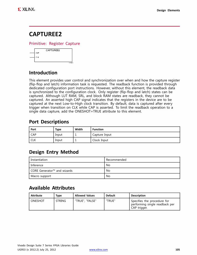
Design Elements
CAPTUREE2Primitive: Register Capture
IntroductionThis element provides user control and synchronization over when and how the capture register(flip-flop and latch) information task is requested. The readback function is provided throughdedicated configuration port instructions. However, without this element, the readback datais synchronized to the configuration clock. Only register (flip-flop and latch) states can becaptured. Although LUT RAM, SRL, and block RAM states are readback, they cannot becaptured. An asserted high CAP signal indicates that the registers in the device are to becaptured at the next Low-to-High clock transition. By default, data is captured after everytrigger when transition on CLK while CAP is asserted. To limit the readback operation to asingle data capture, add the ONESHOT=TRUE attribute to this element.
Port DescriptionsPort Type Width Function
CAP Input 1 Capture Input
CLK Input 1 Clock Input
Design Entry MethodInstantiation Recommended
Inference No
CORE Generator™ and wizards No
Macro support No
Available AttributesAttribute Type Allowed Values Default Description
ONESHOT STRING "TRUE", "FALSE" "TRUE" Specifies the procedure forperforming single readback perCAP trigger.
Vivado Design Suite 7 Series FPGA Libraries GuideUG953 (v 2012.2) July 25, 2012 www.xilinx.com 105

Design Elements
VHDL Instantiation TemplateUnless they already exist, copy the following two statements and paste them before the entitydeclaration.Library UNISIM;use UNISIM.vcomponents.all;
-- CAPTUREE2: Register Capture-- 7 Series-- Xilinx HDL Libraries Guide, version 2012.2
CAPTUREE2_inst : CAPTUREE2generic map (
ONESHOT=> "TRUE" -- Specifies the procedure for performing single readback per CAP trigger.)port map (
CAP => CAP, -- 1-bit input: Capture InputCLK => CLK -- 1-bit input: Clock Input
);
-- End of CAPTUREE2_inst instantiation
Verilog Instantiation Template
// CAPTUREE2: Register Capture// 7 Series// Xilinx HDL Libraries Guide, version 2012.2
CAPTUREE2#(.ONESHOT("TRUE") // Specifies the procedure for performing single readback per CAP trigger.
)CAPTUREE2_inst (
.CAP(CAP), // 1-bit input: Capture Input
.CLK(CLK) // 1-bit input: Clock Input);
// End of CAPTUREE2_inst instantiation
For More InformationSee the 7 series FPGA User Documentation (User Guides and Data Sheets).
Vivado Design Suite 7 Series FPGA Libraries GuideUG953 (v 2012.2) July 25, 2012 www.xilinx.com 106
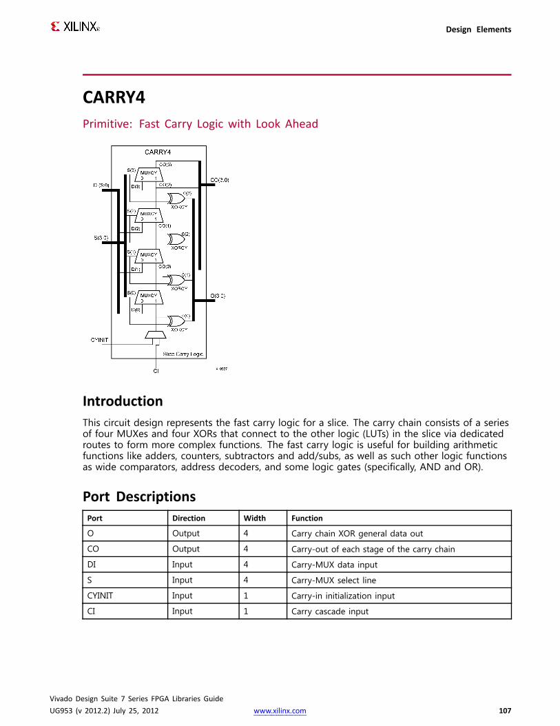
Design Elements
CARRY4Primitive: Fast Carry Logic with Look Ahead
IntroductionThis circuit design represents the fast carry logic for a slice. The carry chain consists of a seriesof four MUXes and four XORs that connect to the other logic (LUTs) in the slice via dedicatedroutes to form more complex functions. The fast carry logic is useful for building arithmeticfunctions like adders, counters, subtractors and add/subs, as well as such other logic functionsas wide comparators, address decoders, and some logic gates (specifically, AND and OR).
Port DescriptionsPort Direction Width Function
O Output 4 Carry chain XOR general data out
CO Output 4 Carry-out of each stage of the carry chain
DI Input 4 Carry-MUX data input
S Input 4 Carry-MUX select line
CYINIT Input 1 Carry-in initialization input
CI Input 1 Carry cascade input
Vivado Design Suite 7 Series FPGA Libraries GuideUG953 (v 2012.2) July 25, 2012 www.xilinx.com 107

Design Elements
Design Entry MethodInstantiation Yes
Inference Recommended
CORE Generator™ and wizards No
Macro support No
VHDL Instantiation TemplateUnless they already exist, copy the following two statements and paste them before the entitydeclaration.Library UNISIM;use UNISIM.vcomponents.all;
-- CARRY4: Fast Carry Logic Component-- 7 Series-- Xilinx HDL Libraries Guide, version 2012.2
CARRY4_inst : CARRY4port map (
CO => CO, -- 4-bit carry outO => O, -- 4-bit carry chain XOR data outCI => CI, -- 1-bit carry cascade inputCYINIT => CYINIT, -- 1-bit carry initializationDI => DI, -- 4-bit carry-MUX data inS => S -- 4-bit carry-MUX select input
);
-- End of CARRY4_inst instantiation
Verilog Instantiation Template
// CARRY4: Fast Carry Logic Component// 7 Series// Xilinx HDL Libraries Guide, version 2012.2
CARRY4CARRY4_inst (.CO(CO), // 4-bit carry out.O(O), // 4-bit carry chain XOR data out.CI(CI), // 1-bit carry cascade input.CYINIT(CYINIT), // 1-bit carry initialization.DI(DI), // 4-bit carry-MUX data in.S(S) // 4-bit carry-MUX select input
);
// End of CARRY4_inst instantiation
For More InformationSee the 7 series FPGA User Documentation (User Guides and Data Sheets).
Vivado Design Suite 7 Series FPGA Libraries GuideUG953 (v 2012.2) July 25, 2012 www.xilinx.com 108

Design Elements
CFGLUT5Primitive: 5-input Dynamically Reconfigurable Look-Up Table (LUT)
IntroductionThis element is a runtime, dynamically reconfigurable, 5-input look-up table (LUT) that enablesthe changing of the logical function of the LUT during circuit operation. Using the CDI pin, anew INIT value can be synchronously shifted in serially to change the logical function. The O6output pin produces the logical output function, based on the current INIT value loaded intothe LUT and the currently selected I0-I4 input pins. Optionally, you can use the O5 output incombination with the O6 output to create two individual 4-input functions sharing the sameinputs or a 5-input function and a 4-input function that uses a subset of the 5-input logic (seetables below). This component occupies one of the four LUT6 components within a Slice-M.
To cascade this element, connect the CDO pin from each element to the CDI input of thenext element. This will allow a single serial chain of data (32-bits per LUT) to reconfiguremultiple LUTs.
Port DescriptionsPort Direction Width Function
O6 Output 1 5-LUT output
O5 Output 1 4-LUT output
I0, I1, I2, I3, I4 Input 1 LUT inputs
CDO Output 1 Reconfiguration data cascaded output (optionally connect to theCDI input of a subsequent LUT)
CDI Input 1 Reconfiguration data serial input
CLK Input 1 Reconfiguration clock
CE Input 1 Active high reconfiguration clock enable
Vivado Design Suite 7 Series FPGA Libraries GuideUG953 (v 2012.2) July 25, 2012 www.xilinx.com 109
Design Elements
Design Entry MethodInstantiation Recommended
Inference No
CORE Generator™ and wizards No
Macro support No
• Connect the CLK input to the clock source used to supply the reconfiguration data.
• Connect the CDI input to the source of the reconfiguration data.
• Connect the CE pin to the active high logic if you need to enable/disable LUTreconfiguration.
• Connect the I4-I0 pins to the source inputs to the logic equation. The logic function isoutput on O6 and O5.
• To cascade this element, connect the CDO pin from each element to the CDI input ofthe next element to allow a single serial chain of data to reconfigure multiple LUTs.
The INIT attribute should be placed on this design element to specify the initial logical functionof the LUT. A new INIT can be loaded into the LUT any time during circuit operation byshifting in 32-bits per LUT in the chain, representing the new INIT value. Disregard the O6 andO5 output data until all 32-bits of new INIT data has been clocked into the LUT. The logicalfunction of the LUT changes as new INIT data is shifted into it. Data should be shifted in MSB(INIT[31]) first and LSB (INIT[0]) last.
In order to understand the O6 and O5 logical value based on the current INIT, see the tablebelow:
I4 I3 I2 I1 I0 O6 Value O5 Value
1 1 1 1 1 INIT[31] INIT[15]
1 1 1 1 0 INIT[30] INIT[14]. . . . . . . . .
1 0 0 0 1 INIT[17] INIT[1]
1 0 0 0 0 INIT[16] INIT[0]
0 1 1 1 1 INIT[15] INIT[15]
0 1 1 1 0 INIT[14] INIT[14]. . . . . . . . .
0 0 0 0 1 INIT[1] INIT[1]
0 0 0 0 0 INIT[0] INIT[0]
For instance, the INIT value of FFFF8000 would represent the following logical equations:
• O6 = I4 or (I3 and I2 and I1 and I0)
• O5 = I3 and I2 and I1 and I0
To use these elements as two, 4-input LUTs with the same inputs but different functions, tie theI4 signal to a logical one. The INIT[31:16] values apply to the logical values of the O6 outputand INIT [15:0] apply to the logical values of the O5 output.
Vivado Design Suite 7 Series FPGA Libraries GuideUG953 (v 2012.2) July 25, 2012 www.xilinx.com 110

Design Elements
Available AttributesAttribute Data Type Allowed Values Default Description
INIT Hexadecimal Any 32-bit Value All zeros Specifies the initial logicalexpression of this element.
VHDL Instantiation TemplateUnless they already exist, copy the following two statements and paste them before the entitydeclaration.Library UNISIM;use UNISIM.vcomponents.all;
-- CFGLUT5: Reconfigurable 5-input LUT (Mapped to SliceM LUT6)-- 7 Series-- Xilinx HDL Libraries Guide, version 2012.2
CFGLUT5_inst : CFGLUT5generic map (
INT => X"00000000")port map (
CDO=> CDO, -- Reconfiguration cascade outputO5 => O5, -- 4-LUT outputO6 => O6, -- 5-LUT outputCDI => CDI, -- Reconfiguration data inputCE => CE, -- Reconfiguration enable inputCLK => CLK, -- Clock inputI0 => I0, -- Logic data inputI1 => I1, -- Logic data inputI2 => I2, -- Logic data inputI3 => I3, -- Logic data inputI4 => I4 -- Logic data input
);
-- End of CFGLUT5_inst instantiation
Verilog Instantiation Template
// CFGLUT5: Reconfigurable 5-input LUT (Mapped to a SliceM LUT6)// 7 Series// Xilinx HDL Libraries Guide, version 2012.2
CFGLUT5 #(.INIT(32'h00000000) // Specify initial LUT contents
) CFGLUT5_inst (.CDO(CDO), // Reconfiguration cascade output.O5(O5), // 4-LUT output.O6(O6), // 5-LUT output.CDI(CDI), // Reconfiguration data input.CE(CE), // Reconfiguration enable input.CLK(CLK), // Clock input.I0(I0), // Logic data input.I1(I1), // Logic data input.I2(I2), // Logic data input.I3(I3), // Logic data input.I4(I4) // Logic data input
);
// End of CFGLUT5_inst instantiation
Vivado Design Suite 7 Series FPGA Libraries GuideUG953 (v 2012.2) July 25, 2012 www.xilinx.com 111

Design Elements
For More InformationSee the 7 series FPGA User Documentation (User Guides and Data Sheets).
Vivado Design Suite 7 Series FPGA Libraries GuideUG953 (v 2012.2) July 25, 2012 www.xilinx.com 112

Design Elements
DCIRESETPrimitive: Digitally Controlled Impedance Reset Component
IntroductionThis design element is used to reset the Digitally Controlled Impedance (DCI) state machineafter configuration has been completed. By toggling the RST input to the DCIRESET primitivewhile the device is operating, the DCI state-machine is reset and both phases of impedanceadjustment proceed in succession. All I/Os using DCI will be unavailable until the LOCKEDoutput from the DCIRESET block is asserted
Port DescriptionsPort Type Width Function
LOCKED Output 1 DCI state-machine LOCK status output.When low, DCI I/O impedance is beingcalibrated and DCI I/Os are unavailable.Upon a low-to-high assertion, DCI I/Osare available for use.
RST Input 1 Active-high asynchronous reset inputto DCI state-machine. After RST isasserted, I/Os utilizing DCI will beunavailable until LOCKED is asserted.
Design Entry MethodInstantiation Yes
Inference No
CORE Generator™ and wizards No
Macro support No
VHDL Instantiation TemplateUnless they already exist, copy the following two statements and paste them before the entitydeclaration.Library UNISIM;use UNISIM.vcomponents.all;
-- DCIRESET: Digitally Controlled Impedance Reset Component-- 7 Series-- Xilinx HDL Libraries Guide, version 2012.2
DCIRESET_inst : DCIRESET
Vivado Design Suite 7 Series FPGA Libraries GuideUG953 (v 2012.2) July 25, 2012 www.xilinx.com 113

Design Elements
port map (LOCKED=> LOCKED, -- 1-bit output: LOCK status outputRST => RST -- 1-bit input: Active-high asynchronous reset input
);
-- End of DCIRESET_inst instantiation
Verilog Instantiation Template
// DCIRESET: Digitally Controlled Impedance Reset Component// 7 Series// Xilinx HDL Libraries Guide, version 2012.2
DCIRESET DCIRESET_inst (.LOCKED(LOCKED), // 1-bit output: LOCK status output.RST(RST) // 1-bit input: Active-high asynchronous reset input
);
// End of DCIRESET_inst instantiation
For More InformationSee the 7 series FPGA User Documentation (User Guides and Data Sheets).
Vivado Design Suite 7 Series FPGA Libraries GuideUG953 (v 2012.2) July 25, 2012 www.xilinx.com 114

Design Elements
DNA_PORTPrimitive: Device DNA Access Port
IntroductionThe DNA_PORT allows access to a dedicated shift register that can be loaded with theDevice DNA data bits (factory-programmed, read-only unique ID) for a given 7 series device.In addition to shifting out the DNA data bits, this component allows for the inclusion ofsupplemental bits of your data, or allows for the DNA data to rollover (repeat DNA data afterinitial data has been shifted out). This component is primarily used in conjunction with othercircuitry to build added copy protection for the FPGA bitstream from possible theft. Connect allinputs and outputs to the design to ensure proper operation. To access the Device DNA data,you must first load the shift register by setting the active high READ signal for one clock cycle.After the shift register is loaded, the data can be synchronously shifted out by enabling theactive high SHIFT input and capturing the data out the DOUT output port. Additional datacan be appended to the end of the 57-bit shift register by connecting the appropriate logicto the DIN port. If DNA data rollover is desired, connect the DOUT port directly to the DINport to allow for the same data to be shifted out after completing the 57-bit shift operation.If no additional data is necessary, the DIN port can be tied to a logic zero. The attributeSIM_DNA_VALUE can be optionally set to allow for simulation of a possible DNA data sequence.By default, the Device DNA data bits are all zeros in the simulation model.
Port DescriptionsPort Type Width Function
CLK Input 1 Clock input.
DIN Input 1 User data input pin.
DOUT Output 1 DNA output data.
READ Input 1 Active high load DNA, active low read input.
SHIFT Input 1 Active high shift enable input.
Vivado Design Suite 7 Series FPGA Libraries GuideUG953 (v 2012.2) July 25, 2012 www.xilinx.com 115

Design Elements
Design Entry MethodInstantiation Recommended
Inference No
CORE Generator™ and wizards No
Macro support No
Available AttributesAttribute Type Allowed Values Default Description
SIM_DNA _VALUE HEX 57'h000000000000000to57'h1ffffffffffffff
57'h000000000000000Specifies a sample 57-bit DNA valuefor simulation
VHDL Instantiation TemplateUnless they already exist, copy the following two statements and paste them before the entitydeclaration.Library UNISIM;use UNISIM.vcomponents.all;
-- DNA_PORT: Device DNA Access Port-- 7 Series-- Xilinx HDL Libraries Guide, version 2012.2
DNA_PORT_inst : DNA_PORTgeneric map (
SIM_DNA_VALUE=> X"000000000000000" -- Specifies a sample 57-bit DNA value for simulation)port map (
DOUT=> DOUT, -- 1-bit output: DNA output data.CLK => CLK, -- 1-bit input: Clock input.DIN => DIN, -- 1-bit input: User data input pin.READ => READ, -- 1-bit input: Active high load DNA, active low read input.SHIFT => SHIFT -- 1-bit input: Active high shift enable input.
);
-- End of DNA_PORT_inst instantiation
Verilog Instantiation Template
// DNA_PORT: Device DNA Access Port// 7 Series// Xilinx HDL Libraries Guide, version 2012.2
DNA_PORT#(.SIM_DNA_VALUE(57'h000000000000000) // Specifies a sample 57-bit DNA value for simulation
)DNA_PORT_inst (
.DOUT(DOUT), // 1-bit output: DNA output data.
.CLK(CLK), // 1-bit input: Clock input.
.DIN(DIN), // 1-bit input: User data input pin.
.READ(READ), // 1-bit input: Active high load DNA, active low read input.
.SHIFT(SHIFT) // 1-bit input: Active high shift enable input.);
// End of DNA_PORT_inst instantiation
Vivado Design Suite 7 Series FPGA Libraries GuideUG953 (v 2012.2) July 25, 2012 www.xilinx.com 116

Design Elements
For More InformationSee the 7 series FPGA User Documentation (User Guides and Data Sheets).
Vivado Design Suite 7 Series FPGA Libraries GuideUG953 (v 2012.2) July 25, 2012 www.xilinx.com 117
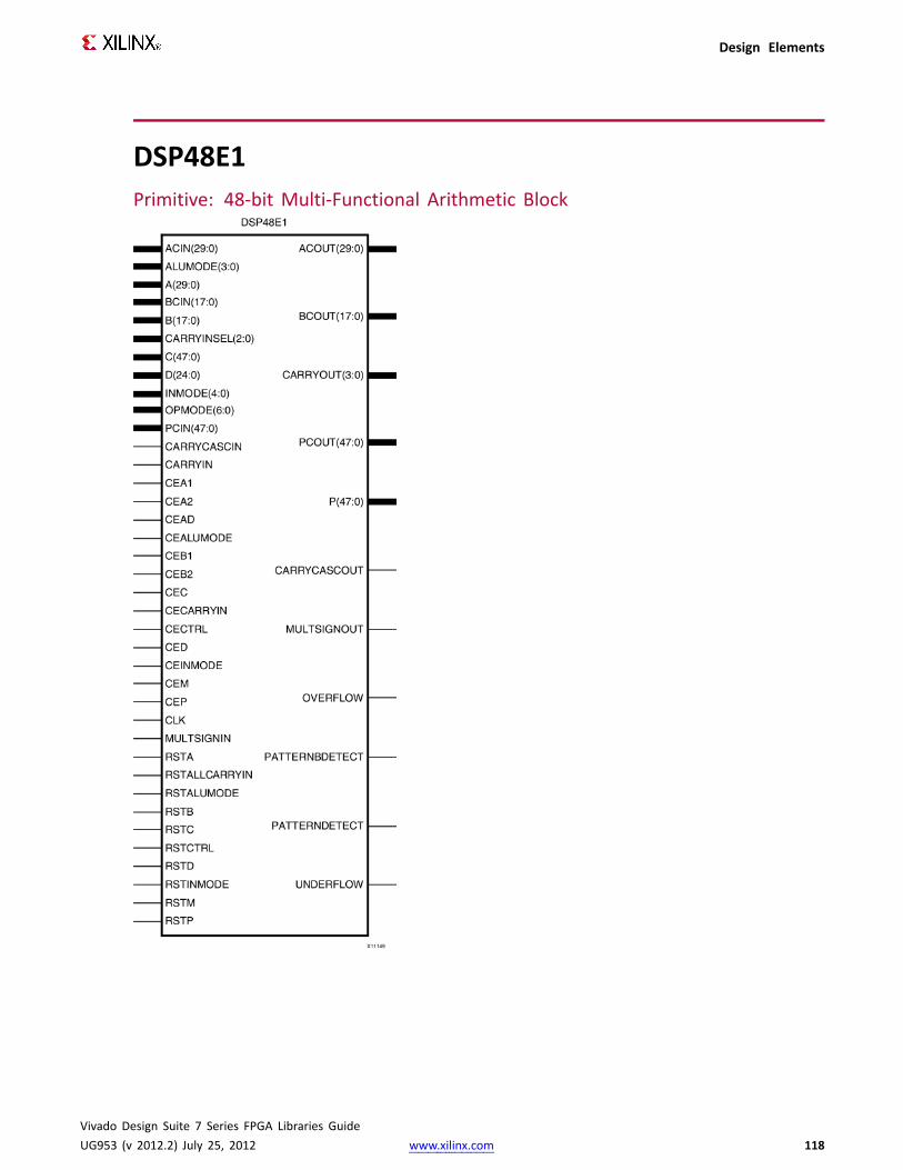
Design Elements
DSP48E1Primitive: 48-bit Multi-Functional Arithmetic Block
Vivado Design Suite 7 Series FPGA Libraries GuideUG953 (v 2012.2) July 25, 2012 www.xilinx.com 118

Design Elements
IntroductionThis design element is a versatile, scalable, hard IP block within 7 series devices that allows forthe creation of compact, high-speed, arithmetic-intensive operations, such as those seen formany DSP algorithms. Some of the functions capable within the block include multiplication,addition, subtraction, accumulation, shifting, logical operations and pattern detection.
Port DescriptionsPort Type Width Function
A<29:0> Input 30 Data input for preadder, multiplier,adder/subtractor/accumulator, ALU or concatenationoperations. When used with the multiplier or preadder, 25bits of data (A[24:0]) is used and upper bits (A[29:25]) areunused and may be tied to ground. When using the internaladder/subctractor/accumulator or ALU circuit, all 30 bits areused (A[29:0]). When used in concatenation mode, all 30bits are used and this constitutes the MSB (upper) bitsof the concatenated vector.
ACIN<29:0> Input 30 Cascaded data input from ACOUT of previous DSP48E1 slice(muxed with A). If not used, tie port to all zeros.
ACOUT<29:0> Output 30 Cascaded data output to ACIN of next DSP48E1 slice. Ifnot used, leave unconnected.
ALUMODE<3:0> Input 4 Controls the selection of the logic function in the DSP48E1slice.
B<17:0> Input 18 The B input of the multiplier. B[17:0] are the least significantbits (LSBs) of the A:B concatenated input to the second-stageadder/subtracter or logic function.
BCIN<17:0> Input 18 Cascaded data input from BCOUT of previous DSP48E1 slice(muxed with B). If not used, tie port to all zeros.
BCOUT<17:0> Output 18 Cascaded data output to BCIN of next DSP48E1 slice. If notused, leave unconnected.
C<47:0> Input 48 Data input to the second-stage adder/subtracter, patterndetector, or logic function.
CARRYCASCIN Input 1 Cascaded carry input from CARRYCASCOUT of previousDSP48E1 slice.
CARRYCASCOUT Output 1 Cascaded carry output to CARRYCASCIN of next DSP48E1slice. This signal is internally fed back into the CARRYINSELmultiplexer input of the same DSP48E1 slice.
CARRYIN Input 1 Carry input from the FPGA logic.
Vivado Design Suite 7 Series FPGA Libraries GuideUG953 (v 2012.2) July 25, 2012 www.xilinx.com 119
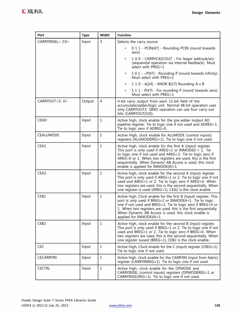
Design Elements
Port Type Width Function
CARRYINSEL< 2:0> Input 3 Selects the carry source:
• 0 1 1 - PCIN[47] - Rounding PCIN (round towardszero)
• 1 0 0 - CARRYCASCOUT - For larger add/sub/acc(sequential operation via internal feedback). Mustselect with PREG=1
• 1 0 1 - ~P[47] - Rounding P (round towards infinity).Must select with PREG=1
• 1 1 0 - A[24] - XNOR B[17] Rounding A x B
• 1 1 1 - P[47] - For rounding P (round towards zero).Must select with PREG=1
CARRYOUT<3: 0> Output 4 4-bit carry output from each 12-bit field of theaccumulate/adder/logic unit. Normal 48-bit operation usesonly CARRYOUT3. SIMD operation can use four carry outbits (CARRYOUT[3:0]).
CEAD Input 1 Active high, clock enable for the pre-adder output ADpipeline register. Tie to logic one if not used and ADREG=1.Tie to logic zero if ADREG=0.
CEALUMODE Input 1 Active High, clock enable for ALUMODE (control inputs)registers (ALUMODEREG=1). Tie to logic one if not used.
CEA1 Input 1 Active high, clock enable for the first A (input) register.This port is only used if AREG=2 or INMODE0 = 1. Tieto logic one if not used and AREG=2. Tie to logic zero ifAREG=0 or 1. When two registers are used, this is the firstsequentially. When Dynamic AB Access is used, this clockenable is applied for INMODE[0]=1.
CEA2 Input 1 Active high, clock enable for the second A (input) register.This port is only used if AREG=1 or 2. Tie to logic one if notused and AREG=1 or 2. Tie to logic zero if AREG=0. Whentwo registers are used, this is the second sequentially. Whenone register is used (AREG=1), CEA2 is the clock enable.
CEB1 Input 1 Active high, Clock enable for the first B (input) register. Thisport is only used if BREG=2 or INMODE4=1. Tie to logicone if not used and BREG=2. Tie to logic zero if BREG=0 or1. When two registers are used, this is the first sequentially.When Dynamic AB Access is used, this clock enable isapplied for INMODE[4]=1.
CEB2 Input 1 Active high, clock enable for the second B (input) register.This port is only used if BREG=1 or 2. Tie to logic one if notused and BREG=1 or 2. Tie to logic zero if BREG=0. Whentwo registers are used, this is the second sequentially. Whenone register isused (BREG=1), CEB2 is the clock enable.
CEC Input 1 Active High, Clock enable for the C (input) register (CREG=1).Tie to logic one if not used.
CECARRYIN Input 1 Active high, clock enable for the CARRYIN (input from fabric)register (CARRYINREG=1). Tie to logic one if not used.
CECTRL Input 1 Active high, clock enable for the OPMODE andCARRYINSEL (control inputs) registers (OPMODEREG=1 orCARRYINSELREG=1). Tie to logic one if not used.
Vivado Design Suite 7 Series FPGA Libraries GuideUG953 (v 2012.2) July 25, 2012 www.xilinx.com 120

Design Elements
Port Type Width Function
CED Input 1 Active high, Clock enable for the D (input) registers(DREG=1). Tie to logic one if not used.
CEINMODE Input 1 Active high, clock enable for the INMODE control inputregisters (INMODEREG=1). Tie to logic one if not used.
CEM Input 1 Active high, Clock enable for the post-multiply M (pipeline)register and the internal multiply round CARRYIN register(MREG=1). Tie to logic one if not used.
CEP Input 1 Active high, clock enable for the P (output) register(PREG=1). Tie to logic one if not used.
CLK Input 1 This port is the DSP48E1 input clock, common to all internalregisters and flip-flops.
D<24:0> Input 25 25-bit data input to the pre-adder or alternative input to themultiplier. The pre-adder implements D + A as determinedby the INMODE3 signal.
INMODE<4:0> Input 5 These five control bits select the functionality of thepre-adder, the A, B, and D inputs, and the input registers.These bits should be tied to all zeroes if not used.
MULTSIGNIN Input 1 Sign of the multiplied result from the previous DSP48E1 slicefor MACC extension. Either connect to the MULTSIGNOUTof another DSP block or tie to ground if not used.
MULTSIGNOUT Output 1 Sign of the multiplied result cascaded to the next DSP48E1slice for MACC extension. Either connect to the MULTSIGNINof another DSP block or tie to ground if not used.
OPMODE<6:0> Input 7 Controls the input to the X, Y, and Z multiplexers in theDSP48E1 slice dictating the operation or function of theDSP slice.
OVERFLOW Output 1 Active high Overflow indicator when used with theappropriate setting of the pattern detector and PREG=1.
P<47:0> Output 48 Data output from second stage adder/subtracter or logicfunction.
PATTERNBDET ECT Output 1 Active high match indicator between P[47:0] and the patternbar.
PATTERNDETE CT Output 1 Active high Match indicator between P[47:0] and the patterngated by the MASK. Result arrives on the same cycle as P.
PCIN<47:0> Input 48 Cascaded data input from PCOUT of previous DSP48E1 sliceto adder. If used, connect to PCOUT of upstream cascadedDSP slice. If not used, tie port to all zeros.
PCOUT<47:0> Output 48 Cascaded data output to PCIN of next DSP48E1 slice. Ifused, connect to PCIN of downstream cascaded DSP slice. Ifnot used, leave unconnected.
RSTA Input 1 Active high, synchronous Reset for both A (input) registers(AREG=1 or 2). Tie to logic zero if not used.
RSTALLCARRY IN Input 1 Active high, synchronous reset for the Carry (internal path)and the CARRYIN registers (CARRYINREG=1). Tie to logiczero if not used.
Vivado Design Suite 7 Series FPGA Libraries GuideUG953 (v 2012.2) July 25, 2012 www.xilinx.com 121

Design Elements
Port Type Width Function
RSTALUMODE Input 1 Active high, synchronous Reset for ALUMODE (controlinputs) registers (ALUMODEREG=1). Tie to logic zero if notused.
RSTB Input 1 Active high, synchronous Reset for both B (input) registers(BREG=1 or 2). Tie to logic zero if not used.
RSTC Input 1 Active high, synchronous reset for the C (input) registers(CREG=1). Tie to logic zero if not used.
RSTCTRL Input 1 Active High, synchronous reset for OPMODE andCARRYINSEL (control inputs) registers (OPMODEREG=1and/or CARRYINSELREG=1). Tie to logic zero if not used.
RSTD Input 1 Active high, synchronous reset for the D (input) register andfor the pre-adder (output) AD pipeline register (DREG=1and/or ADREG=1). Tie to logic zero if not used.
RSTINMODE Input 1 Active high, synchronous reset for the INMODE (controlinput) registers (INMODEREG=1). Tie to logic zero if notused.
RSTM Input 1 Active high, synchronous reset for the M (pipeline) registers(MREG=1). Tie to logic zero if not used.
RSTP Input 1 Active high, synchronous reset for the P (output) registers(PREG=1). Tie to logic zero if not used.
UNDERFLOW Output 1 Active high underflow indicator when used with theappropriate setting of the pattern detector and PREG=1.
Design Entry MethodInstantiation Yes
Inference Recommended
CORE Generator™ and wizards Yes
Macro support Yes
Available AttributesAttribute Type Allowed Values Default Description
ACASCREG DECIMAL 1, 0, 2 1 In conjunction with AREG, selects thenumber of A input registers on the Acascade path, ACOUT. This attribute mustbe equal to or one less than the AREGvalue: AREG=0: ACASCREG must be 0AREG=1: ACASCREG must be 1 AREG=2:ACASCREG can be 1 or 2
ADREG DECIMAL 1, 0 1 Selects the number of AD pipeline registers.Set to 1 to use the AD pipeline registers.
A_INPUT STRING "DIRECT","CASCADE"
"DIRECT" Selects the input to the A port betweenparallel input ("DIRECT") or the cascadedinput from the previous slice ("CASCADE").
Vivado Design Suite 7 Series FPGA Libraries GuideUG953 (v 2012.2) July 25, 2012 www.xilinx.com 122
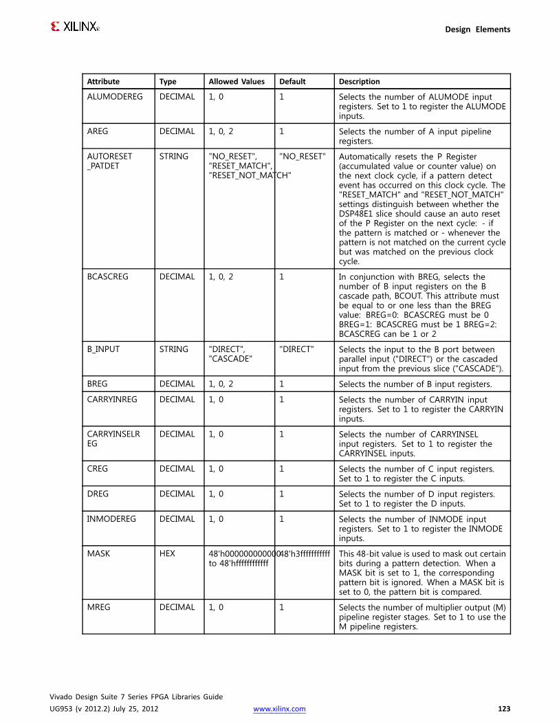
Design Elements
Attribute Type Allowed Values Default Description
ALUMODEREG DECIMAL 1, 0 1 Selects the number of ALUMODE inputregisters. Set to 1 to register the ALUMODEinputs.
AREG DECIMAL 1, 0, 2 1 Selects the number of A input pipelineregisters.
AUTORESET_PATDET
STRING "NO_RESET","RESET_MATCH","RESET_NOT_MATCH"
"NO_RESET" Automatically resets the P Register(accumulated value or counter value) onthe next clock cycle, if a pattern detectevent has occurred on this clock cycle. The"RESET_MATCH" and "RESET_NOT_MATCH"settings distinguish between whether theDSP48E1 slice should cause an auto resetof the P Register on the next cycle: - ifthe pattern is matched or - whenever thepattern is not matched on the current cyclebut was matched on the previous clockcycle.
BCASCREG DECIMAL 1, 0, 2 1 In conjunction with BREG, selects thenumber of B input registers on the Bcascade path, BCOUT. This attribute mustbe equal to or one less than the BREGvalue: BREG=0: BCASCREG must be 0BREG=1: BCASCREG must be 1 BREG=2:BCASCREG can be 1 or 2
B_INPUT STRING "DIRECT","CASCADE"
"DIRECT" Selects the input to the B port betweenparallel input ("DIRECT") or the cascadedinput from the previous slice ("CASCADE").
BREG DECIMAL 1, 0, 2 1 Selects the number of B input registers.
CARRYINREG DECIMAL 1, 0 1 Selects the number of CARRYIN inputregisters. Set to 1 to register the CARRYINinputs.
CARRYINSELREG
DECIMAL 1, 0 1 Selects the number of CARRYINSELinput registers. Set to 1 to register theCARRYINSEL inputs.
CREG DECIMAL 1, 0 1 Selects the number of C input registers.Set to 1 to register the C inputs.
DREG DECIMAL 1, 0 1 Selects the number of D input registers.Set to 1 to register the D inputs.
INMODEREG DECIMAL 1, 0 1 Selects the number of INMODE inputregisters. Set to 1 to register the INMODEinputs.
MASK HEX 48'h000000000000to 48'hffffffffffff
48'h3fffffffffff This 48-bit value is used to mask out certainbits during a pattern detection. When aMASK bit is set to 1, the correspondingpattern bit is ignored. When a MASK bit isset to 0, the pattern bit is compared.
MREG DECIMAL 1, 0 1 Selects the number of multiplier output (M)pipeline register stages. Set to 1 to use theM pipeline registers.
Vivado Design Suite 7 Series FPGA Libraries GuideUG953 (v 2012.2) July 25, 2012 www.xilinx.com 123

Design Elements
Attribute Type Allowed Values Default Description
OPMODEREG DECIMAL 1, 0 1 Selects the number of OPMODE inputregisters. Set to 1 to register the OPMODEinputs.
PATTERN HEX 48'h000000000000to 48'hffffffffffff
48'h000000000000This 48-bit value is used in the patterndetector.
PREG DECIMAL 1, 0 1 Selects the number of P output registers.Set to 1 to register the P outputs. Theregistered outputs will include CARRYOUT,CARRYCASCOUT, MULTSIGNOUT,PATTERNB_DETECT, PATTERN_DETECT, andPCOUT.
SEL_MASK STRING "MASK", "C","ROUNDING_MODE1","ROUNDING_MODE2"
"MASK" Selects the mask to be used for thepattern detector. The C and MASK settingsare for standard uses of the patterndetector (counter, overflow detection, etc.).ROUNDING_MODE1 (Cbar left shifted by 1)and ROUNDING_MODE2 (C-bar left shiftedby 2) select special masks based off ofthe optionally registered C port. Theserounding modes can be used to implementconvergent rounding in the DSP48E1 sliceusing the pattern detector.
SEL_PATTERN STRING "PATTERN", "C" "PATTERN" Selects the input source for the patternfield. The input source can either be a48-bit dynamic C input or a 48-bit staticPATTERN attribute field.
USE_DPORT BOOLEAN FALSE, TRUE FALSE Determines whether the pre-adder and theD Port are used or not.
USE_MULT STRING "MULTIPLY","DYNAMIC","NONE"
"MULTIPLY" Selects usage of the multiplier. Set to"NONE" to save power when using onlythe Adder/Logic Unit. The "DYNAMIC"setting indicates that the user is switchingbetween A*B and A:B operations on the flyand therefore needs to get the worst-casetiming of the two paths.
USE_PATTERN_DETECT
STRING "NO_PATDET","PATDET"
"NO_PATDET" Selects whether the pattern detector andrelated features are used ("PATDET") or notused ("NO_PATDET"). This attribute is usedfor speed specification and SimulationModel purposes only.
USE_SIMD STRING "ONE48","FOUR12","TWO24"
"ONE48" Selects the mode of operation for theadder/subtracter. The attribute setting canbe one 48-bit adder mode ("ONE48"), two24- bit adder mode ("TWO24"), or four12-bit adder mode ("FOUR12"). Selecting"ONE48" mode is compatible with Virtex-5DSP48 operation and is not actually atrue SIMD mode. Typical Multiply-Addoperations are supported when the modeis set to "ONE48". When either "TWO24" or"FOUR12" mode is selected, the multipliermust not be used, and USE_MULT must beset to "NONE".
Vivado Design Suite 7 Series FPGA Libraries GuideUG953 (v 2012.2) July 25, 2012 www.xilinx.com 124

Design Elements
VHDL Instantiation TemplateUnless they already exist, copy the following two statements and paste them before the entitydeclaration.Library UNISIM;use UNISIM.vcomponents.all;
-- DSP48E1: 48-bit Multi-Functional Arithmetic Block-- 7 Series-- Xilinx HDL Libraries Guide, version 2012.2
DSP48E1_inst : DSP48E1generic map (
-- Feature Control Attributes: Data Path SelectionA_INPUT => "DIRECT", -- Selects A input source, "DIRECT" (A port) or "CASCADE" (ACIN port)B_INPUT => "DIRECT", -- Selects B input source, "DIRECT" (B port) or "CASCADE" (BCIN port)USE_DPORT=> FALSE, -- Select D port usage (TRUE or FALSE)USE_MULT=> "MULTIPLY", -- Select multiplier usage ("MULTIPLY", "DYNAMIC", or "NONE")-- Pattern Detector Attributes: Pattern Detection ConfigurationAUTORESET_PATDET=> "NO_RESET", -- "NO_RESET", "RESET_MATCH", "RESET_NOT_MATCH"MASK=> X"3fffffffffff", -- 48-bit mask value for pattern detect (1=ignore)PATTERN=> X"000000000000", -- 48-bit pattern match for pattern detectSEL_MASK=> "MASK", -- "C", "MASK", "ROUNDING_MODE1", "ROUNDING_MODE2"SEL_PATTERN=> "PATTERN", -- Select pattern value ("PATTERN" or "C")USE_PATTERN_DETECT=> "NO_PATDET", -- Enable pattern detect ("PATDET" or "NO_PATDET")-- Register Control Attributes: Pipeline Register ConfigurationACASCREG=> 1, -- Number of pipeline stages between A/ACIN and ACOUT(0, 1 or 2)ADREG=> 1, -- Number of pipeline stages for pre-adder (0 or 1)ALUMODEREG=> 1, -- Number of pipeline stages for ALUMODE(0 or 1)AREG=> 1, -- Number of pipeline stages for A (0, 1 or 2)BCASCREG=> 1, -- Number of pipeline stages between B/BCIN and BCOUT(0, 1 or 2)BREG=> 1, -- Number of pipeline stages for B (0, 1 or 2)CARRYINREG=> 1, -- Number of pipeline stages for CARRYIN (0 or 1)CARRYINSELREG=> 1, -- Number of pipeline stages for CARRYINSEL (0 or 1)CREG=> 1, -- Number of pipeline stages for C (0 or 1)DREG=> 1, -- Number of pipeline stages for D (0 or 1)INMODEREG=> 1, -- Number of pipeline stages for INMODE (0 or 1)MREG=> 1, -- Number of multiplier pipeline stages (0 or 1)OPMODEREG=> 1, -- Number of pipeline stages for OPMODE(0 or 1)PREG=> 1, -- Number of pipeline stages for P (0 or 1)USE_SIMD => "ONE48" -- SIMD selection ("ONE48", "TWO24", "FOUR12")
)port map (
-- Cascade: 30-bit (each) output: Cascade PortsACOUT=> ACOUT, -- 30-bit output: A port cascade outputBCOUT=> BCOUT, -- 18-bit output: B port cascade outputCARRYCASCOUT=> CARRYCASCOUT, -- 1-bit output: Cascade carry outputMULTSIGNOUT=> MULTSIGNOUT, -- 1-bit output: Multiplier sign cascade outputPCOUT=> PCOUT, -- 48-bit output: Cascade output-- Control: 1-bit (each) output: Control Inputs/Status BitsOVERFLOW=> OVERFLOW, -- 1-bit output: Overflow in add/acc outputPATTERNBDETECT=> PATTERNBDETECT,-- 1-bit output: Pattern bar detect outputPATTERNDETECT=> PATTERNDETECT, -- 1-bit output: Pattern detect outputUNDERFLOW=> UNDERFLOW, -- 1-bit output: Underflow in add/acc output-- Data: 4-bit (each) output: Data PortsCARRYOUT=> CARRYOUT, -- 4-bit output: Carry outputP => P, -- 48-bit output: Primary data output-- Cascade: 30-bit (each) input: Cascade PortsACIN => ACIN, -- 30-bit input: A cascade data inputBCIN => BCIN, -- 18-bit input: B cascade inputCARRYCASCIN=> CARRYCASCIN, -- 1-bit input: Cascade carry inputMULTSIGNIN => MULTSIGNIN, -- 1-bit input: Multiplier sign inputPCIN => PCIN, -- 48-bit input: P cascade input-- Control: 4-bit (each) input: Control Inputs/Status BitsALUMODE=> ALUMODE, -- 4-bit input: ALU control inputCARRYINSEL => CARRYINSEL, -- 3-bit input: Carry select inputCEINMODE=> CEINMODE, -- 1-bit input: Clock enable input for INMODEREGCLK => CLK, -- 1-bit input: Clock inputINMODE => INMODE, -- 5-bit input: INMODE control inputOPMODE=> OPMODE, -- 7-bit input: Operation mode input
Vivado Design Suite 7 Series FPGA Libraries GuideUG953 (v 2012.2) July 25, 2012 www.xilinx.com 125

Design Elements
RSTINMODE=> RSTINMODE, -- 1-bit input: Reset input for INMODEREG-- Data: 30-bit (each) input: Data PortsA => A, -- 30-bit input: A data inputB => B, -- 18-bit input: B data inputC => C, -- 48-bit input: C data inputCARRYIN => CARRYIN, -- 1-bit input: Carry input signalD => D, -- 25-bit input: D data input-- Reset/Clock Enable: 1-bit (each) input: Reset/Clock Enable InputsCEA1 => CEA1, -- 1-bit input: Clock enable input for 1st stage AREGCEA2 => CEA2, -- 1-bit input: Clock enable input for 2nd stage AREGCEAD => CEAD, -- 1-bit input: Clock enable input for ADREGCEALUMODE=> CEALUMODE, -- 1-bit input: Clock enable input for ALUMODERECEB1 => CEB1, -- 1-bit input: Clock enable input for 1st stage BREGCEB2 => CEB2, -- 1-bit input: Clock enable input for 2nd stage BREGCEC => CEC, -- 1-bit input: Clock enable input for CREGCECARRYIN=> CECARRYIN, -- 1-bit input: Clock enable input for CARRYINREGCECTRL => CECTRL, -- 1-bit input: Clock enable input for OPMODEREGand CARRYINSELREGCED => CED, -- 1-bit input: Clock enable input for DREGCEM=> CEM, -- 1-bit input: Clock enable input for MREGCEP => CEP, -- 1-bit input: Clock enable input for PREGRSTA => RSTA, -- 1-bit input: Reset input for AREGRSTALLCARRYIN=> RSTALLCARRYIN, -- 1-bit input: Reset input for CARRYINREGRSTALUMODE=> RSTALUMODE, -- 1-bit input: Reset input for ALUMODEREGRSTB => RSTB, -- 1-bit input: Reset input for BREGRSTC => RSTC, -- 1-bit input: Reset input for CREGRSTCTRL => RSTCTRL, -- 1-bit input: Reset input for OPMODEREGand CARRYINSELREGRSTD => RSTD, -- 1-bit input: Reset input for DREGand ADREGRSTM=> RSTM, -- 1-bit input: Reset input for MREGRSTP => RSTP -- 1-bit input: Reset input for PREG
);
-- End of DSP48E1_inst instantiation
Verilog Instantiation Template
// DSP48E1: 48-bit Multi-Functional Arithmetic Block// 7 Series// Xilinx HDL Libraries Guide, version 2012.2
DSP48E1 #(// Feature Control Attributes: Data Path Selection.A_INPUT("DIRECT"), // Selects A input source, "DIRECT" (A port) or "CASCADE" (ACIN port).B_INPUT("DIRECT"), // Selects B input source, "DIRECT" (B port) or "CASCADE" (BCIN port).USE_DPORT("FALSE"), // Select D port usage (TRUE or FALSE).USE_MULT("MULTIPLY"), // Select multiplier usage ("MULTIPLY", "DYNAMIC", or "NONE")// Pattern Detector Attributes: Pattern Detection Configuration.AUTORESET_PATDET("NO_RESET"), // "NO_RESET", "RESET_MATCH", "RESET_NOT_MATCH".MASK(48'h3fffffffffff), // 48-bit mask value for pattern detect (1=ignore).PATTERN(48'h000000000000), // 48-bit pattern match for pattern detect.SEL_MASK("MASK"), // "C", "MASK", "ROUNDING_MODE1", "ROUNDING_MODE2".SEL_PATTERN("PATTERN"), // Select pattern value ("PATTERN" or "C").USE_PATTERN_DETECT("NO_PATDET"), // Enable pattern detect ("PATDET" or "NO_PATDET")// Register Control Attributes: Pipeline Register Configuration.ACASCREG(1), // Number of pipeline stages between A/ACIN and ACOUT(0, 1 or 2).ADREG(1), // Number of pipeline stages for pre-adder (0 or 1).ALUMODEREG(1), // Number of pipeline stages for ALUMODE(0 or 1).AREG(1), // Number of pipeline stages for A (0, 1 or 2).BCASCREG(1), // Number of pipeline stages between B/BCIN and BCOUT(0, 1 or 2).BREG(1), // Number of pipeline stages for B (0, 1 or 2).CARRYINREG(1), // Number of pipeline stages for CARRYIN (0 or 1).CARRYINSELREG(1), // Number of pipeline stages for CARRYINSEL (0 or 1).CREG(1), // Number of pipeline stages for C (0 or 1).DREG(1), // Number of pipeline stages for D (0 or 1).INMODEREG(1), // Number of pipeline stages for INMODE (0 or 1).MREG(1), // Number of multiplier pipeline stages (0 or 1).OPMODEREG(1), // Number of pipeline stages for OPMODE(0 or 1).PREG(1), // Number of pipeline stages for P (0 or 1).USE_SIMD("ONE48") // SIMD selection ("ONE48", "TWO24", "FOUR12")
)DSP48E1_inst (
Vivado Design Suite 7 Series FPGA Libraries GuideUG953 (v 2012.2) July 25, 2012 www.xilinx.com 126

Design Elements
// Cascade: 30-bit (each) output: Cascade Ports.ACOUT(ACOUT), // 30-bit output: A port cascade output.BCOUT(BCOUT), // 18-bit output: B port cascade output.CARRYCASCOUT(CARRYCASCOUT), // 1-bit output: Cascade carry output.MULTSIGNOUT(MULTSIGNOUT), // 1-bit output: Multiplier sign cascade output.PCOUT(PCOUT), // 48-bit output: Cascade output// Control: 1-bit (each) output: Control Inputs/Status Bits.OVERFLOW(OVERFLOW), // 1-bit output: Overflow in add/acc output.PATTERNBDETECT(PATTERNBDETECT),// 1-bit output: Pattern bar detect output.PATTERNDETECT(PATTERNDETECT), // 1-bit output: Pattern detect output.UNDERFLOW(UNDERFLOW), // 1-bit output: Underflow in add/acc output// Data: 4-bit (each) output: Data Ports.CARRYOUT(CARRYOUT), // 4-bit output: Carry output.P(P), // 48-bit output: Primary data output// Cascade: 30-bit (each) input: Cascade Ports.ACIN(ACIN), // 30-bit input: A cascade data input.BCIN(BCIN), // 18-bit input: B cascade input.CARRYCASCIN(CARRYCASCIN), // 1-bit input: Cascade carry input.MULTSIGNIN(MULTSIGNIN), // 1-bit input: Multiplier sign input.PCIN(PCIN), // 48-bit input: P cascade input// Control: 4-bit (each) input: Control Inputs/Status Bits.ALUMODE(ALUMODE), // 4-bit input: ALU control input.CARRYINSEL(CARRYINSEL), // 3-bit input: Carry select input.CEINMODE(CEINMODE), // 1-bit input: Clock enable input for INMODEREG.CLK(CLK), // 1-bit input: Clock input.INMODE(INMODE), // 5-bit input: INMODE control input.OPMODE(OPMODE), // 7-bit input: Operation mode input.RSTINMODE(RSTINMODE), // 1-bit input: Reset input for INMODEREG// Data: 30-bit (each) input: Data Ports.A(A), // 30-bit input: A data input.B(B), // 18-bit input: B data input.C(C), // 48-bit input: C data input.CARRYIN(CARRYIN), // 1-bit input: Carry input signal.D(D), // 25-bit input: D data input// Reset/Clock Enable: 1-bit (each) input: Reset/Clock Enable Inputs.CEA1(CEA1), // 1-bit input: Clock enable input for 1st stage AREG.CEA2(CEA2), // 1-bit input: Clock enable input for 2nd stage AREG.CEAD(CEAD), // 1-bit input: Clock enable input for ADREG.CEALUMODE(CEALUMODE), // 1-bit input: Clock enable input for ALUMODERE.CEB1(CEB1), // 1-bit input: Clock enable input for 1st stage BREG.CEB2(CEB2), // 1-bit input: Clock enable input for 2nd stage BREG.CEC(CEC), // 1-bit input: Clock enable input for CREG.CECARRYIN(CECARRYIN), // 1-bit input: Clock enable input for CARRYINREG.CECTRL(CECTRL), // 1-bit input: Clock enable input for OPMODEREGand CARRYINSELREG.CED(CED), // 1-bit input: Clock enable input for DREG.CEM(CEM), // 1-bit input: Clock enable input for MREG.CEP(CEP), // 1-bit input: Clock enable input for PREG.RSTA(RSTA), // 1-bit input: Reset input for AREG.RSTALLCARRYIN(RSTALLCARRYIN), // 1-bit input: Reset input for CARRYINREG.RSTALUMODE(RSTALUMODE), // 1-bit input: Reset input for ALUMODEREG.RSTB(RSTB), // 1-bit input: Reset input for BREG.RSTC(RSTC), // 1-bit input: Reset input for CREG.RSTCTRL(RSTCTRL), // 1-bit input: Reset input for OPMODEREGand CARRYINSELREG.RSTD(RSTD), // 1-bit input: Reset input for DREGand ADREG.RSTM(RSTM), // 1-bit input: Reset input for MREG.RSTP(RSTP) // 1-bit input: Reset input for PREG
);
// End of DSP48E1_inst instantiation
For More InformationSee the 7 series FPGA User Documentation (User Guides and Data Sheets).
Vivado Design Suite 7 Series FPGA Libraries GuideUG953 (v 2012.2) July 25, 2012 www.xilinx.com 127

Design Elements
EFUSE_USRPrimitive: 32-bit non-volatile design ID
IntroductionProvides internal access to the 32 non-volatile, user-programmable eFUSE bits
Port DescriptionsPort Type Width Function
EFUSEUSR<31 :0> Output 32 User eFUSE register value output
Design Entry MethodInstantiation Recommended
Inference No
CORE Generator™ and wizards No
Macro support No
Available AttributesAttribute Type Allowed Values Default Description
SIM_EFUSE _VALUE HEX 32'h00000000to 32'hffffffff
32'h00000000 Value of the 32-bit non-volatilevalue used in simulation
VHDL Instantiation TemplateUnless they already exist, copy the following two statements and paste them before the entitydeclaration.Library UNISIM;use UNISIM.vcomponents.all;
-- EFUSE_USR: 32-bit non-volatile design ID-- 7 Series-- Xilinx HDL Libraries Guide, version 2012.2
EFUSE_USR_inst : EFUSE_USRgeneric map (
SIM_EFUSE_VALUE=> X"00000000" -- Value of the 32-bit non-volatile value used in simulation)port map (
EFUSEUSR=> EFUSEUSR -- 32-bit output: User eFUSE register value output);
Vivado Design Suite 7 Series FPGA Libraries GuideUG953 (v 2012.2) July 25, 2012 www.xilinx.com 128

Design Elements
-- End of EFUSE_USR_inst instantiation
Verilog Instantiation Template
// EFUSE_USR: 32-bit non-volatile design ID// 7 Series// Xilinx HDL Libraries Guide, version 2012.2
EFUSE_USR#(.SIM_EFUSE_VALUE(32'h00000000) // Value of the 32-bit non-volatile value used in simulation
)EFUSE_USR_inst (
.EFUSEUSR(EFUSEUSR) // 32-bit output: User eFUSE register value output);
// End of EFUSE_USR_inst instantiation
For More InformationSee the 7 series FPGA User Documentation (User Guides and Data Sheets).
Vivado Design Suite 7 Series FPGA Libraries GuideUG953 (v 2012.2) July 25, 2012 www.xilinx.com 129
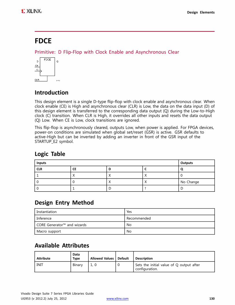
Design Elements
FDCEPrimitive: D Flip-Flop with Clock Enable and Asynchronous Clear
IntroductionThis design element is a single D-type flip-flop with clock enable and asynchronous clear. Whenclock enable (CE) is High and asynchronous clear (CLR) is Low, the data on the data input (D) ofthis design element is transferred to the corresponding data output (Q) during the Low-to-Highclock (C) transition. When CLR is High, it overrides all other inputs and resets the data output(Q) Low. When CE is Low, clock transitions are ignored.
This flip-flop is asynchronously cleared, outputs Low, when power is applied. For FPGA devices,power-on conditions are simulated when global set/reset (GSR) is active. GSR defaults toactive-High but can be inverted by adding an inverter in front of the GSR input of theSTARTUP_E2 symbol.
Logic TableInputs Outputs
CLR CE D C Q
1 X X X 0
0 0 X X No Change
0 1 D ↑ D
Design Entry MethodInstantiation Yes
Inference Recommended
CORE Generator™ and wizards No
Macro support No
Available Attributes
AttributeDataType Allowed Values Default Description
INIT Binary 1, 0 0 Sets the initial value of Q output afterconfiguration.
Vivado Design Suite 7 Series FPGA Libraries GuideUG953 (v 2012.2) July 25, 2012 www.xilinx.com 130

Design Elements
VHDL Instantiation TemplateUnless they already exist, copy the following two statements and paste them before the entitydeclaration.Library UNISIM;use UNISIM.vcomponents.all;
-- FDCE: Single Data Rate D Flip-Flop with Asynchronous Clear and-- Clock Enable (posedge clk).-- 7 Series-- Xilinx HDL Libraries Guide, version 2012.2
FDCE_inst : FDCEgeneric map (
INIT => '0') -- Initial value of register ('0' or '1')port map (
Q => Q, -- Data outputC => C, -- Clock inputCE => CE, -- Clock enable inputCLR => CLR, -- Asynchronous clear inputD => D -- Data input
);
-- End of FDCE_inst instantiation
Verilog Instantiation Template
// FDCE: Single Data Rate D Flip-Flop with Asynchronous Clear and// Clock Enable (posedge clk).// 7 Series// Xilinx HDL Libraries Guide, version 2012.2
FDCE #(.INIT(1'b0) // Initial value of register (1'b0 or 1'b1)
) FDCE_inst (.Q(Q), // 1-bit Data output.C(C), // 1-bit Clock input.CE(CE), // 1-bit Clock enable input.CLR(CLR), // 1-bit Asynchronous clear input.D(D) // 1-bit Data input
);
// End of FDCE_inst instantiation
For More InformationSee the 7 series FPGA User Documentation (User Guides and Data Sheets).
Vivado Design Suite 7 Series FPGA Libraries GuideUG953 (v 2012.2) July 25, 2012 www.xilinx.com 131

Design Elements
FDPEPrimitive: D Flip-Flop with Clock Enable and Asynchronous Preset
IntroductionThis design element is a single D-type flip-flop with data (D), clock enable (CE), andasynchronous preset (PRE) inputs and data output (Q). The asynchronous PRE, when High,overrides all other inputs and sets the (Q) output High. Data on the (D) input is loaded intothe flip-flop when PRE is Low and CE is High on the Low-to-High clock (C) transition. WhenCE is Low, the clock transitions are ignored.
For FPGA devices, this flip-flop is asynchronously preset, output High, when power is applied.Power-on conditions are simulated when global set/reset (GSR) is active. GSR defaults toactive-High but can be inverted by adding an inverter in front of the GSR input of theSTARTUP_E2 symbol.
Logic TableInputs Outputs
PRE CE D C Q
1 X X X 1
0 0 X X No Change
0 1 D ↑ D
Design Entry MethodInstantiation Yes
Inference Recommended
CORE Generator™ and wizards No
Macro support No
Available Attributes
AttributeDataType Allowed Values Default Description
INIT Binary 0, 1 1 Sets the initial value of Q output afterconfiguration
Vivado Design Suite 7 Series FPGA Libraries GuideUG953 (v 2012.2) July 25, 2012 www.xilinx.com 132

Design Elements
VHDL Instantiation TemplateUnless they already exist, copy the following two statements and paste them before the entitydeclaration.Library UNISIM;use UNISIM.vcomponents.all;
-- FDPE: Single Data Rate D Flip-Flop with Asynchronous Preset and-- Clock Enable (posedge clk).-- 7 Series-- Xilinx HDL Libraries Guide, version 2012.2
FDPE_inst : FDPEgeneric map (
INIT => '0') -- Initial value of register ('0' or '1')port map (
Q => Q, -- Data outputC => C, -- Clock inputCE => CE, -- Clock enable inputPRE => PRE, -- Asynchronous preset inputD => D -- Data input
);
-- End of FDPE_inst instantiation
Verilog Instantiation Template
// FDPE: Single Data Rate D Flip-Flop with Asynchronous Preset and// Clock Enable (posedge clk).// 7 Series// Xilinx HDL Libraries Guide, version 2012.2
FDPE #(.INIT(1'b0) // Initial value of register (1'b0 or 1'b1)
) FDPE_inst (.Q(Q), // 1-bit Data output.C(C), // 1-bit Clock input.CE(CE), // 1-bit Clock enable input.PRE(PRE), // 1-bit Asynchronous preset input.D(D) // 1-bit Data input
);
// End of FDPE_inst instantiation
For More InformationSee the 7 series FPGA User Documentation (User Guides and Data Sheets).
Vivado Design Suite 7 Series FPGA Libraries GuideUG953 (v 2012.2) July 25, 2012 www.xilinx.com 133

Design Elements
FDREPrimitive: D Flip-Flop with Clock Enable and Synchronous Reset
IntroductionThis design element is a single D-type flip-flop with data (D), clock enable (CE), and synchronousreset (R) inputs and data output (Q). The synchronous reset (R) input, when High, overridesall other inputs and resets the (Q) output Low on the Low-to-High clock (C) transition. Thedata on the (D) input is loaded into the flip-flop when R is Low and CE is High during theLow-to-High clock transition.
This flip-flop is asynchronously cleared, outputs Low, when power is applied. For FPGA devices,power-on conditions are simulated when global set/reset (GSR) is active. GSR defaults toactive-High but can be inverted by adding an inverter in front of the GSR input of theSTARTUP_E2 symbol.
Logic TableInputs Outputs
R CE D C Q
1 X X ↑ 0
0 0 X X No Change
0 1 D ↑ D
Design Entry MethodInstantiation Yes
Inference Recommended
CORE Generator™ and wizards No
Macro support No
Available Attributes
AttributeDataType Allowed Values Default Description
INIT Binary 0, 1 0 Sets the initial value of Q output afterconfiguration
Vivado Design Suite 7 Series FPGA Libraries GuideUG953 (v 2012.2) July 25, 2012 www.xilinx.com 134
Design Elements
VHDL Instantiation TemplateUnless they already exist, copy the following two statements and paste them before the entitydeclaration.Library UNISIM;use UNISIM.vcomponents.all;
-- FDRE: Single Data Rate D Flip-Flop with Synchronous Reset and-- Clock Enable (posedge clk).-- 7 Series-- Xilinx HDL Libraries Guide, version 2012.2
FDRE_inst : FDREgeneric map (
INIT => '0') -- Initial value of register ('0' or '1')port map (
Q => Q, -- Data outputC => C, -- Clock inputCE => CE, -- Clock enable inputR => R, -- Synchronous reset inputD => D -- Data input
);
-- End of FDRE_inst instantiation
Verilog Instantiation Template
// FDRE: Single Data Rate D Flip-Flop with Synchronous Reset and// Clock Enable (posedge clk).// 7 Series// Xilinx HDL Libraries Guide, version 2012.2
FDRE #(.INIT(1'b0) // Initial value of register (1'b0 or 1'b1)
) FDRE_inst (.Q(Q), // 1-bit Data output.C(C), // 1-bit Clock input.CE(CE), // 1-bit Clock enable input.R(R), // 1-bit Synchronous reset input.D(D) // 1-bit Data input
);
// End of FDRE_inst instantiation
For More InformationSee the 7 series FPGA User Documentation (User Guides and Data Sheets).
Vivado Design Suite 7 Series FPGA Libraries GuideUG953 (v 2012.2) July 25, 2012 www.xilinx.com 135

Design Elements
FDSEPrimitive: D Flip-Flop with Clock Enable and Synchronous Set
IntroductionFDSE is a single D-type flip-flop with data (D), clock enable (CE), and synchronous set (S) inputsand data output (Q). The synchronous set (S) input, when High, overrides the clock enable (CE)input and sets the Q output High during the Low-to-High clock (C) transition. The data onthe D input is loaded into the flip-flop when S is Low and CE is High during the Low-to-Highclock (C) transition.
For FPGA devices, this flip-flop is asynchronously preset, output High, when power is applied.Power-on conditions are simulated when global set/reset (GSR) is active. GSR defaults toactive-High but can be inverted by adding an inverter in front of the GSR input of theSTARTUP_E2 symbol.
Logic TableInputs Outputs
S CE D C Q
1 X X ↑ 1
0 0 X X No Change
0 1 D ↑ D
Design Entry MethodInstantiation Yes
Inference Recommended
CORE Generator™ and wizards No
Macro support No
Vivado Design Suite 7 Series FPGA Libraries GuideUG953 (v 2012.2) July 25, 2012 www.xilinx.com 136

Design Elements
Available Attributes
AttributeDataType Allowed Values Default Description
INIT Binary 0, 1 1 Sets the initial value of Q output afterconfiguration
VHDL Instantiation TemplateUnless they already exist, copy the following two statements and paste them before the entitydeclaration.Library UNISIM;use UNISIM.vcomponents.all;
-- FDSE: Single Data Rate D Flip-Flop with Synchronous Set and-- Clock Enable (posedge clk).-- 7 Series-- Xilinx HDL Libraries Guide, version 2012.2
FDSE_inst : FDSEgeneric map (
INIT => '0') -- Initial value of register ('0' or '1')port map (
Q => Q, -- Data outputC => C, -- Clock inputCE => CE, -- Clock enable inputS => S, -- Synchronous Set inputD => D -- Data input
);
-- End of FDSE_inst instantiation
Verilog Instantiation Template
// FDSE: Single Data Rate D Flip-Flop with Synchronous Set and// Clock Enable (posedge clk).// 7 Series// Xilinx HDL Libraries Guide, version 2012.2
FDSE #(.INIT(1'b0) // Initial value of register (1'b0 or 1'b1)
) FDSE_inst (.Q(Q), // 1-bit Data output.C(C), // 1-bit Clock input.CE(CE), // 1-bit Clock enable input.S(S), // 1-bit Synchronous set input.D(D) // 1-bit Data input
);
// End of FDSE_inst instantiation
For More InformationSee the 7 series FPGA User Documentation (User Guides and Data Sheets).
Vivado Design Suite 7 Series FPGA Libraries GuideUG953 (v 2012.2) July 25, 2012 www.xilinx.com 137

Design Elements
FIFO18E1Primitive: 18Kb FIFO (First-In-First-Out) Block RAM Memory
Introduction7 series devices contain several block RAM memories, each of which can be separatelyconfigured as a FIFO, an automatic error-correction RAM, or as a general-purpose 36KB or18KB RAM/ROM memory. These Block RAM memories offer fast and flexible storage of largeamounts of on-chip data. The FIFO18E1 uses the FIFO control logic and the 18KB Block RAM.This primitive can be used in a 4-bit wide by 4K deep, 9-bit wide by 2K deep, 18-bit wide by 1Kdeep, or a 36-bit wide by 512 deep configuration. The primitive can be configured in eithersynchronous or dual-clock (asynchronous) mode, with all associated FIFO flags and statussignals.When using the dual-clock mode with independent clocks, depending on the offset betweenread and write clock edges, the Empty, Almost Empty, Full and Almost Full flags can deassertone cycle later. Due to the asynchronous nature of the clocks the simulation model only reflectsthe deassertion latency cycles listed in the User Guide.Note For a 36-bit wide by 512 deep FIFO, the "FIFO18_36" mode must be used. For deeperor wider configurations of the FIFO, the FIFO36E1 can be used. If error-correction circuitry isdesired, the FIFO36E1 with "FIFO36_72" mode must be used.
Vivado Design Suite 7 Series FPGA Libraries GuideUG953 (v 2012.2) July 25, 2012 www.xilinx.com 138

Design Elements
Port DescriptionsPort Type Width Function
ALMOSTEMPTY Output 1 Programmable flag to indicate the FIFO is almostempty. The ALMOST_EMPTY_OFFSET attributespecifies the threshold where this flag is triggeredrelative to full/empty.
ALMOSTFULL Output 1 Programmable flag to indicate that the FIFO isalmost full. The ALMOST_FULL_OFFSET attributespecifies the threshold where this flag is triggeredrelative to full/empty.
DI<31:0> Input 32 FIFO data input bus.
DIP<3:0> Input 4 FIFO parity data input bus.
DO<31:0> Output 32 FIFO data output bus.
DOP<3:0> Output 4 FIFO parity data output bus.
EMPTY Output 1 Active high logic to indicate that the FIFO is currentlyempty.
FULL Output 1 Active high logic indicates that the FIFO is full.
RDCLK Input 1 Rising edge read clock.
RDCOUNT<11: 0> Output 12 Read count.
RDEN Input 1 Active high FIFO read enable.
RDERR Output 1 Read error occurred.
REGCE Input 1 Output register clock enable for pipelinedsynchronous FIFO. DO_REG must be set to 1 if usingthis enable.
RST Input 1 Active high (FIFO logic) asynchronous reset(for dual-clock FIFO), synchronous reset (forsynchronous FIFO). Must be held for a minimum of5 WRCLK/RDCLK cycles.
RSTREG Input 1 Output register synchronous set/reset. DO_REGmust be set to 1 if using this reset.
WRCLK Input 1 Rising edge write clock.
WRCOUNT<11: 0> Output 12 Write count.
WREN Input 1 Active high FIFO write enable.
WRERR Output 1 Write error occurred. When the FIFO is full, anyadditional write operation generates an error flag.Synchronous with WRCLK.
Design Entry MethodInstantiation Yes
Inference No
CORE Generator™ and wizards Yes
Macro support Recommended
Vivado Design Suite 7 Series FPGA Libraries GuideUG953 (v 2012.2) July 25, 2012 www.xilinx.com 139
Design Elements
Available AttributesAttribute Type Allowed Values Default Description
ALMOST_EMPTY_OFFSET
HEX 13'h0000 to13'h1fff
13'h0080 Specifies the amount of datacontents in the RAM to triggerthe ALMOST_EMPTY flag.
ALMOST_FULL_OFFSET
HEX 13'h0000 to13'h1fff
13'h0080 Specifies the amount of datacontents in the RAM to triggerthe ALMOST_FULL flag.
DATA_WIDTH DECIMAL 4, 9, 18, 36 4 Specifies the desired data widthfor the FIFO.Note If set to 36, FIFO_MODEmust be set to FIFO18_36.
DO_REG DECIMAL 1, 0 1 Data pipeline register for EN_SYN.
EN_SYN BOOLEAN FALSE, TRUE FALSE EN_SYN denotes whether the FIFOis operating in either dual-clock(two independent clocks) orsynchronous (a single clock)mode. Dual-clock must useDO_REG=1.
FIFO_MODE STRING "FIFO18","FIFO18_36"
"FIFO18" Selects "FIFO18" or "FIFO18_36"mode. If set to "FIFO18_36",DATA_WIDTH must be set to 36.
FIRST_WORD_FALL_THROUGH
BOOLEAN FALSE, TRUE FALSE If TRUE, the first write to the FIFOwill appear on DO without a firstRDEN assertion.
INIT HEX 36 bit HEX 36'h000000000 Specifies the initial value on theDO output after configuration.
SIM_DEVICE STRING 7SERIES "7SERIES" Must be set to "7SERIES" inorder to exhibit proper simulationbehavior under all conditions.
SRVAL HEX 36 bit HEX 36'h000000000 Specifies the output value ofthe FIFO upon assertion of thesynchronous reset (RSTREG)signal. Only valid for DO_REG=1.
VHDL Instantiation TemplateUnless they already exist, copy the following two statements and paste them before the entitydeclaration.Library UNISIM;use UNISIM.vcomponents.all;
-- FIFO18E1: 18Kb FIFO (First-In-First-Out) Block RAMMemory-- 7 Series-- Xilinx HDL Libraries Guide, version 2012.2
FIFO18E1_inst : FIFO18E1generic map (
ALMOST_EMPTY_OFFSET=> X"0080", -- Sets the almost empty thresholdALMOST_FULL_OFFSET=> X"0080", -- Sets almost full thresholdDATA_WIDTH=> 4, -- Sets data width to 4-36DO_REG=> 1, -- Enable output register (1-0) Must be 1 if EN_SYN = FALSE
Vivado Design Suite 7 Series FPGA Libraries GuideUG953 (v 2012.2) July 25, 2012 www.xilinx.com 140

Design Elements
EN_SYN => FALSE, -- Specifies FIFO as dual-clock (FALSE) or Synchronous (TRUE)FIFO_MODE=> "FIFO18", -- Sets mode to FIFO18 or FIFO18_36FIRST_WORD_FALL_THROUGH=> FALSE, -- Sets the FIFO FWFT to FALSE, TRUEINIT => X"000000000", -- Initial values on output portSIM_DEVICE => "7SERIES", -- Must be set to "7SERIES" for simulation behaviorSRVAL => X"000000000" -- Set/Reset value for output port
)port map (
-- Read Data: 32-bit (each) output: Read output dataDO => DO, -- 32-bit output: Data outputDOP => DOP, -- 4-bit output: Parity data output-- Status: 1-bit (each) output: Flags and other FIFO status outputsALMOSTEMPTY=> ALMOSTEMPTY,-- 1-bit output: Almost empty flagALMOSTFULL=> ALMOSTFULL, -- 1-bit output: Almost full flagEMPTY=> EMPTY, -- 1-bit output: Empty flagFULL => FULL, -- 1-bit output: Full flagRDCOUNT=> RDCOUNT, -- 12-bit output: Read countRDERR=> RDERR, -- 1-bit output: Read errorWRCOUNT=> WRCOUNT, -- 12-bit output: Write countWRERR=> WRERR, -- 1-bit output: Write error-- Read Control Signals: 1-bit (each) input: Read clock, enable and reset input signalsRDCLK => RDCLK, -- 1-bit input: Read clockRDEN=> RDEN, -- 1-bit input: Read enableREGCE=> REGCE, -- 1-bit input: Clock enableRST => RST, -- 1-bit input: Asynchronous ResetRSTREG=> RSTREG, -- 1-bit input: Output register set/reset-- Write Control Signals: 1-bit (each) input: Write clock and enable input signalsWRCLK=> WRCLK, -- 1-bit input: Write clockWREN=> WREN, -- 1-bit input: Write enable-- Write Data: 32-bit (each) input: Write input dataDI => DI, -- 32-bit input: Data inputDIP => DIP -- 4-bit input: Parity input
);
-- End of FIFO18E1_inst instantiation
Vivado Design Suite 7 Series FPGA Libraries GuideUG953 (v 2012.2) July 25, 2012 www.xilinx.com 141
Design Elements
Verilog Instantiation Template
// FIFO18E1: 18Kb FIFO (First-In-First-Out) Block RAMMemory// 7 Series// Xilinx HDL Libraries Guide, version 2012.2
FIFO18E1 #(.ALMOST_EMPTY_OFFSET(13'h0080), // Sets the almost empty threshold.ALMOST_FULL_OFFSET(13'h0080), // Sets almost full threshold.DATA_WIDTH(4), // Sets data width to 4-36.DO_REG(1), // Enable output register (1-0) Must be 1 if EN_SYN = FALSE.EN_SYN("FALSE"), // Specifies FIFO as dual-clock (FALSE) or Synchronous (TRUE).FIFO_MODE("FIFO18"), // Sets mode to FIFO18 or FIFO18_36.FIRST_WORD_FALL_THROUGH("FALSE"), // Sets the FIFO FWFT to FALSE, TRUE.INIT(36'h000000000), // Initial values on output port.SIM_DEVICE("7SERIES"), // Must be set to "7SERIES" for simulation behavior.SRVAL(36'h000000000) // Set/Reset value for output port
)FIFO18E1_inst (
// Read Data: 32-bit (each) output: Read output data.DO(DO), // 32-bit output: Data output.DOP(DOP), // 4-bit output: Parity data output// Status: 1-bit (each) output: Flags and other FIFO status outputs.ALMOSTEMPTY(ALMOSTEMPTY),// 1-bit output: Almost empty flag.ALMOSTFULL(ALMOSTFULL), // 1-bit output: Almost full flag.EMPTY(EMPTY), // 1-bit output: Empty flag.FULL(FULL), // 1-bit output: Full flag.RDCOUNT(RDCOUNT), // 12-bit output: Read count.RDERR(RDERR), // 1-bit output: Read error.WRCOUNT(WRCOUNT), // 12-bit output: Write count.WRERR(WRERR), // 1-bit output: Write error// Read Control Signals: 1-bit (each) input: Read clock, enable and reset input signals.RDCLK(RDCLK), // 1-bit input: Read clock.RDEN(RDEN), // 1-bit input: Read enable.REGCE(REGCE), // 1-bit input: Clock enable.RST(RST), // 1-bit input: Asynchronous Reset.RSTREG(RSTREG), // 1-bit input: Output register set/reset// Write Control Signals: 1-bit (each) input: Write clock and enable input signals.WRCLK(WRCLK), // 1-bit input: Write clock.WREN(WREN), // 1-bit input: Write enable// Write Data: 32-bit (each) input: Write input data.DI(DI), // 32-bit input: Data input.DIP(DIP) // 4-bit input: Parity input
);
// End of FIFO18E1_inst instantiation
For More InformationSee the 7 series FPGA User Documentation (User Guides and Data Sheets).
Vivado Design Suite 7 Series FPGA Libraries GuideUG953 (v 2012.2) July 25, 2012 www.xilinx.com 142

Design Elements
FIFO36E1Primitive: 36Kb FIFO (First-In-First-Out) Block RAM Memory
Introduction7 series devices contain several block RAM memories that can be configured as FIFOs,automatic error-correction RAM, or general-purpose 36KB or 18KB RAM/ROM memories. TheseBlock RAM memories offer fast and flexible storage of large amounts of on-chip data. TheFIFO36E1 allows access to the Block RAM in the 36KB FIFO configurations. This componentcan be configured and used as a 4-bit wide by 8K deep, 9-bit by 4K deep, 18-bit by 2K deep,36-bit wide by 1K deep, or 72-bit wide by 512 deep synchronous or dual-clock (asynchronous)FIFO RAM with all associated FIFO flags. When using the dual-clock mode with independentclocks, depending on the offset between read and write clock edges, the Empty, Almost Empty,Full and Almost Full flags can deassert one cycle later. Due to the asynchronous nature of theclocks the simulation model only reflects the deassertion latency cycles listed in the User Guide.Note For a 72-bit wide by 512 deep FIFO, the "FIFO36_72" mode must be used. For smallerconfigurations of the FIFO, the FIFO18E1 can be used. If error-correction circuitry is desired, the"FIFO36_72" mode must be used.
Vivado Design Suite 7 Series FPGA Libraries GuideUG953 (v 2012.2) July 25, 2012 www.xilinx.com 143

Design Elements
Port DescriptionsPort Type Width Function
ALMOSTEMPTY Output 1 Programmable flag to indicate the FIFO is almostempty. The ALMOST_EMPTY_OFFSET attributespecifies where to trigger this flag.
ALMOSTFULL Output 1 Programmable flag to indicate the FIFO is almostfull. The ALMOST_FULL_OFFSET attribute specifieswhere to trigger this flag.
DBITERR Output 1 Status output from ECC function to indicate adouble bit error was detected. EN_ECC_READ needsto be TRUE in order to use this functionality.
DI<63:0> Input 64 FIFO data input bus.
DIP<7:0> Input 8 FIFO parity data input bus.
DO<63:0> Output 64 FIFO data output bus.
DOP<7:0> Output 8 FIFO parity data output bus.
ECCPARITY<7 :0> Output 8 8-bit data generated by the ECC encoder used bythe ECC decoder for memory error detection andcorrection.
EMPTY Output 1 Active high logic to indicate that the FIFO iscurrently empty.
FULL Output 1 Active high logic indicates that the FIFO is full.
INJECTDBITE RR Input 1 Inject a double bit error if ECC feature is used.
INJECTSBITE RR Input 1 Inject a single bit error if ECC feature is used.
RDCLK Input 1 Rising edge read clock.
RDCOUNT<12: 0> Output 13 Read count.
RDEN Input 1 Active high FIFO read enable.
RDERR Output 1 Read error occurred.
REGCE Input 1 Output register clock enable for pipelinedsynchronous FIFO. DO_REG must be 1 to use thisenable.
RST Input 1 Active high (FIFO logic) asynchronous reset (fordual-clock FIFO), synchronous reset (synchronousFIFO) for 5 CLK cycles.
RSTREG Input 1 Output register synchronous set/reset. DO_REGmust be 1 to use this reset.
SBITERR Output 1 Status output from ECC function to indicate a singlebit error was detected. EN_ECC_READ needs to beTRUE in order to use this functionality.
WRCLK Input 1 Write clock and enable input signals
WRCOUNT<12: 0> Output 13 Write count.
WREN Input 1 Active high FIFO write enable.
WRERR Output 1 Write error occurred. When the FIFO is full, anyadditional write operation generates an error flag.Synchronous with WRCLK.
Vivado Design Suite 7 Series FPGA Libraries GuideUG953 (v 2012.2) July 25, 2012 www.xilinx.com 144
Design Elements
Design Entry MethodInstantiation Yes
Inference No
CORE Generator™ and wizards Yes
Macro support Recommended
Available AttributesAttribute Type Allowed Values Default Description
ALMOST_EMPTY_OFFSET
HEX 13'h0000 to13'h1fff
13'h0080 Specifies the amount of datacontents in the RAM to triggerthe ALMOST_EMPTY flag.
ALMOST_FULL _OFFSET HEX 13'h0000 to13'h1fff
13'h0080 Specifies the amount of datacontents in the RAM to triggerthe ALMOST_FULL flag.
DATA_WIDTH DECIMAL 4, 9, 18, 36, 72 4 Specifies the desired data widthfor the FIFO. For data widths of72, FIFO_MODE must be set to"FIFO36_72"
DO_REG DECIMAL 1, 0 1 Enable output register to theFIFO for improved clock-to-outtiming at the expense of addedread latency (one pipeline delay).DO_REG must be 1 when EN_SYNis set to FALSE.
EN_ECC_READ BOOLEAN FALSE, TRUE FALSE Enable the ECC decoder circuitry.
EN_ECC_WRITE BOOLEAN FALSE, TRUE FALSE Enable the ECC encoder circuitry.
EN_SYN BOOLEAN FALSE, TRUE FALSE When FALSE, specifies the FIFO tobe used in asynchronous mode(two independent clock) or whenTRUE in synchronous (a singleclock) operation.
FIFO_MODE STRING "FIFO36","FIFO36_72"
"FIFO36" Selects regular "FIFO36" or thewide "FIFO36_72" mode. If setto "FIFO36_72", the DATA_WIDTHattribute has to be 72.
FIRST_WORD_FALL_THROUGH
BOOLEAN FALSE, TRUE FALSE If TRUE, the first write to the FIFOwill appear on DO without anRDEN assertion.
INIT HEX 72 bit HEX 72'h000000000000000000
Specifies the initial value on theDO output after configuration.
SIM_DEVICE STRING 7SERIES "7SERIES" Must be set to "7SERIES" inorder to exhibit proper simulationbehavior under all conditions.
SRVAL HEX 72 bit HEX 72'h000000000000000000
Specifies the output value ofthe FIFO upon assertion of thesynchronous reset (RSTREG)signal. Only valid for DO_REG=1.
Vivado Design Suite 7 Series FPGA Libraries GuideUG953 (v 2012.2) July 25, 2012 www.xilinx.com 145
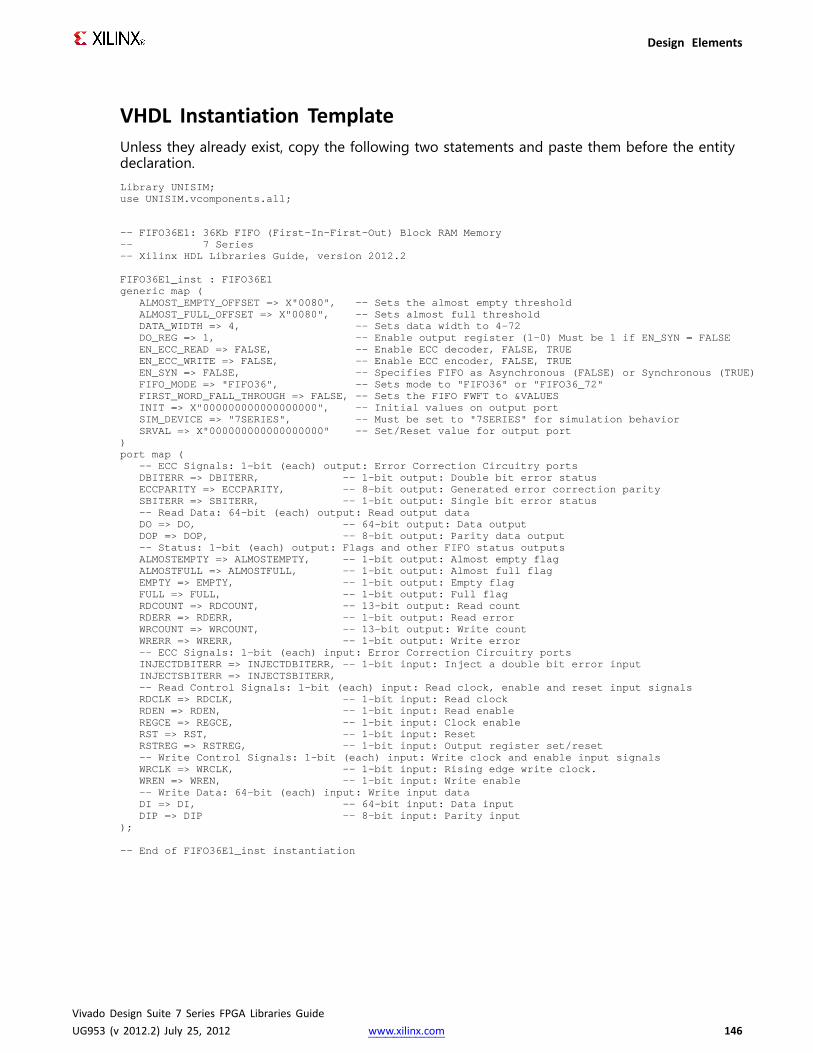
Design Elements
VHDL Instantiation TemplateUnless they already exist, copy the following two statements and paste them before the entitydeclaration.Library UNISIM;use UNISIM.vcomponents.all;
-- FIFO36E1: 36Kb FIFO (First-In-First-Out) Block RAMMemory-- 7 Series-- Xilinx HDL Libraries Guide, version 2012.2
FIFO36E1_inst : FIFO36E1generic map (
ALMOST_EMPTY_OFFSET=> X"0080", -- Sets the almost empty thresholdALMOST_FULL_OFFSET=> X"0080", -- Sets almost full thresholdDATA_WIDTH=> 4, -- Sets data width to 4-72DO_REG=> 1, -- Enable output register (1-0) Must be 1 if EN_SYN = FALSEEN_ECC_READ=> FALSE, -- Enable ECC decoder, FALSE, TRUEEN_ECC_WRITE=> FALSE, -- Enable ECC encoder, FALSE, TRUEEN_SYN => FALSE, -- Specifies FIFO as Asynchronous (FALSE) or Synchronous (TRUE)FIFO_MODE=> "FIFO36", -- Sets mode to "FIFO36" or "FIFO36_72"FIRST_WORD_FALL_THROUGH=> FALSE, -- Sets the FIFO FWFT to &VALUESINIT => X"000000000000000000", -- Initial values on output portSIM_DEVICE => "7SERIES", -- Must be set to "7SERIES" for simulation behaviorSRVAL => X"000000000000000000" -- Set/Reset value for output port
)port map (
-- ECC Signals: 1-bit (each) output: Error Correction Circuitry portsDBITERR => DBITERR, -- 1-bit output: Double bit error statusECCPARITY => ECCPARITY, -- 8-bit output: Generated error correction paritySBITERR => SBITERR, -- 1-bit output: Single bit error status-- Read Data: 64-bit (each) output: Read output dataDO => DO, -- 64-bit output: Data outputDOP => DOP, -- 8-bit output: Parity data output-- Status: 1-bit (each) output: Flags and other FIFO status outputsALMOSTEMPTY=> ALMOSTEMPTY, -- 1-bit output: Almost empty flagALMOSTFULL=> ALMOSTFULL, -- 1-bit output: Almost full flagEMPTY=> EMPTY, -- 1-bit output: Empty flagFULL => FULL, -- 1-bit output: Full flagRDCOUNT=> RDCOUNT, -- 13-bit output: Read countRDERR=> RDERR, -- 1-bit output: Read errorWRCOUNT=> WRCOUNT, -- 13-bit output: Write countWRERR=> WRERR, -- 1-bit output: Write error-- ECC Signals: 1-bit (each) input: Error Correction Circuitry portsINJECTDBITERR => INJECTDBITERR, -- 1-bit input: Inject a double bit error inputINJECTSBITERR => INJECTSBITERR,-- Read Control Signals: 1-bit (each) input: Read clock, enable and reset input signalsRDCLK => RDCLK, -- 1-bit input: Read clockRDEN=> RDEN, -- 1-bit input: Read enableREGCE=> REGCE, -- 1-bit input: Clock enableRST => RST, -- 1-bit input: ResetRSTREG=> RSTREG, -- 1-bit input: Output register set/reset-- Write Control Signals: 1-bit (each) input: Write clock and enable input signalsWRCLK=> WRCLK, -- 1-bit input: Rising edge write clock.WREN=> WREN, -- 1-bit input: Write enable-- Write Data: 64-bit (each) input: Write input dataDI => DI, -- 64-bit input: Data inputDIP => DIP -- 8-bit input: Parity input
);
-- End of FIFO36E1_inst instantiation
Vivado Design Suite 7 Series FPGA Libraries GuideUG953 (v 2012.2) July 25, 2012 www.xilinx.com 146

Design Elements
Verilog Instantiation Template
// FIFO36E1: 36Kb FIFO (First-In-First-Out) Block RAMMemory// 7 Series// Xilinx HDL Libraries Guide, version 2012.2
FIFO36E1 #(.ALMOST_EMPTY_OFFSET(13'h0080), // Sets the almost empty threshold.ALMOST_FULL_OFFSET(13'h0080), // Sets almost full threshold.DATA_WIDTH(4), // Sets data width to 4-72.DO_REG(1), // Enable output register (1-0) Must be 1 if EN_SYN = FALSE.EN_ECC_READ("FALSE"), // Enable ECC decoder, FALSE, TRUE.EN_ECC_WRITE("FALSE"), // Enable ECC encoder, FALSE, TRUE.EN_SYN("FALSE"), // Specifies FIFO as Asynchronous (FALSE) or Synchronous (TRUE).FIFO_MODE("FIFO36"), // Sets mode to "FIFO36" or "FIFO36_72".FIRST_WORD_FALL_THROUGH("FALSE"), // Sets the FIFO FWFT to &VALUES.INIT(72'h000000000000000000), // Initial values on output port.SIM_DEVICE("7SERIES"), // Must be set to "7SERIES" for simulation behavior.SRVAL(72'h000000000000000000) // Set/Reset value for output port
)FIFO36E1_inst (
// ECC Signals: 1-bit (each) output: Error Correction Circuitry ports.DBITERR(DBITERR), // 1-bit output: Double bit error status.ECCPARITY(ECCPARITY), // 8-bit output: Generated error correction parity.SBITERR(SBITERR), // 1-bit output: Single bit error status// Read Data: 64-bit (each) output: Read output data.DO(DO), // 64-bit output: Data output.DOP(DOP), // 8-bit output: Parity data output// Status: 1-bit (each) output: Flags and other FIFO status outputs.ALMOSTEMPTY(ALMOSTEMPTY), // 1-bit output: Almost empty flag.ALMOSTFULL(ALMOSTFULL), // 1-bit output: Almost full flag.EMPTY(EMPTY), // 1-bit output: Empty flag.FULL(FULL), // 1-bit output: Full flag.RDCOUNT(RDCOUNT), // 13-bit output: Read count.RDERR(RDERR), // 1-bit output: Read error.WRCOUNT(WRCOUNT), // 13-bit output: Write count.WRERR(WRERR), // 1-bit output: Write error// ECC Signals: 1-bit (each) input: Error Correction Circuitry ports.INJECTDBITERR(INJECTDBITERR), // 1-bit input: Inject a double bit error input.INJECTSBITERR(INJECTSBITERR),// Read Control Signals: 1-bit (each) input: Read clock, enable and reset input signals.RDCLK(RDCLK), // 1-bit input: Read clock.RDEN(RDEN), // 1-bit input: Read enable.REGCE(REGCE), // 1-bit input: Clock enable.RST(RST), // 1-bit input: Reset.RSTREG(RSTREG), // 1-bit input: Output register set/reset// Write Control Signals: 1-bit (each) input: Write clock and enable input signals.WRCLK(WRCLK), // 1-bit input: Rising edge write clock..WREN(WREN), // 1-bit input: Write enable// Write Data: 64-bit (each) input: Write input data.DI(DI), // 64-bit input: Data input.DIP(DIP) // 8-bit input: Parity input
);
// End of FIFO36E1_inst instantiation
For More InformationSee the 7 series FPGA User Documentation (User Guides and Data Sheets).
Vivado Design Suite 7 Series FPGA Libraries GuideUG953 (v 2012.2) July 25, 2012 www.xilinx.com 147

Design Elements
FRAME_ECCE2Primitive: Configuration Frame Error Correction
IntroductionThis design element enables the dedicated, built-in Error Correction Code (ECC) for theconfiguration memory of the FPGA. This element contains outputs that allow monitoring of thestatus of the ECC circuitry and the status of the readback CRC circuitry.
Port DescriptionsPort Type Width Function
CRCERROR Output 1 Output indicating a CRC error.
ECCERROR Output 1 Output indicating an ECC error.
ECCERRORSIN GLE Output 1 Output Indicating single-bit Frame ECC error detected.
FAR<25:0> Output 26 Frame Address Register Value output.
SYNBIT<4:0> Output 5 Output bit address of error.
SYNDROME<12 :0> Output 13 Output location of erroneous bit.
SYNDROMEVAL ID Output 1 Frame ECC output indicating the SYNDROME output isvalid.
SYNWORD<6:0> Output 7 Word output in the frame where an ECC error has beendetected.
Design Entry MethodInstantiation Recommended
Inference No
CORE Generator™ and wizards No
Macro support No
Vivado Design Suite 7 Series FPGA Libraries GuideUG953 (v 2012.2) July 25, 2012 www.xilinx.com 148

Design Elements
Available AttributesAttribute Type Allowed Values Default Description
FARSRC STRING "EFAR", "FAR" "EFAR" Determines if the output ofFAR[25:0] configuration registerpoints to the FAR or EFAR. Setsconfiguration option register bitCTL0[7].
FRAME_RBT_IN_FILENAME
STRING "0", "bit", "STRING" "NONE" This file is output by the ICAP_E2model and it contains Frame Datainformation for the Raw Bitstream(RBT) file. The FRAME_ECCE2model will parse this file, calculateECC and output any errorconditions.
VHDL Instantiation TemplateUnless they already exist, copy the following two statements and paste them before the entitydeclaration.Library UNISIM;use UNISIM.vcomponents.all;
-- FRAME_ECCE2:Configuration Frame Error Correction-- 7 Series-- Xilinx HDL Libraries Guide, version 2012.2
FRAME_ECCE2_inst : FRAME_ECCE2generic map (
FARSRC=> "EFAR", -- Determines if the output of FAR[25:0] configuration register points-- to the FAR or EFAR. Sets configuration option register bit CTL0[7].
FRAME_RBT_IN_FILENAME=> "NONE" -- This file is output by the ICAP_E2 model and it contains Frame Data-- information for the Raw Bitstream (RBT) file. The FRAME_ECCE2model-- will parse this file, calculate ECC and output any error conditions.
)port map (
CRCERROR=> CRCERROR, -- 1-bit output: Output indicating a CRC error.ECCERROR=> ECCERROR, -- 1-bit output: Output indicating an ECC error.ECCERRORSINGLE=> ECCERRORSINGLE,-- 1-bit output: Output Indicating single-bit Frame ECC error detected.FAR => FAR, -- 26-bit output: Frame Address Register Value output.SYNBIT => SYNBIT, -- 5-bit output: Output bit address of error.SYNDROME=> SYNDROME, -- 13-bit output: Output location of erroneous bit.SYNDROMEVALID=> SYNDROMEVALID, -- 1-bit output: Frame ECC output indicating the SYNDROMEoutput is
-- valid.
SYNWORD=> SYNWORD -- 7-bit output: Word output in the frame where an ECC error has been-- detected.
);
-- End of FRAME_ECCE2_inst instantiation
Vivado Design Suite 7 Series FPGA Libraries GuideUG953 (v 2012.2) July 25, 2012 www.xilinx.com 149
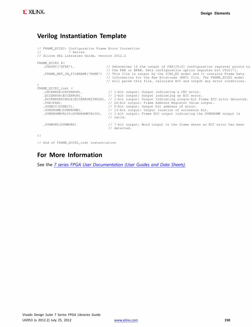
Design Elements
Verilog Instantiation Template
// FRAME_ECCE2:Configuration Frame Error Correction// 7 Series// Xilinx HDL Libraries Guide, version 2012.2
FRAME_ECCE2#(.FARSRC("EFAR"), // Determines if the output of FAR[25:0] configuration register points to
// the FAR or EFAR. Sets configuration option register bit CTL0[7]..FRAME_RBT_IN_FILENAME("NONE") // This file is output by the ICAP_E2 model and it contains Frame Data
// information for the Raw Bitstream (RBT) file. The FRAME_ECCE2model// will parse this file, calculate ECC and output any error conditions.
)FRAME_ECCE2_inst (
.CRCERROR(CRCERROR), // 1-bit output: Output indicating a CRC error.
.ECCERROR(ECCERROR), // 1-bit output: Output indicating an ECC error.
.ECCERRORSINGLE(ECCERRORSINGLE),// 1-bit output: Output Indicating single-bit Frame ECC error detected.
.FAR(FAR), // 26-bit output: Frame Address Register Value output.
.SYNBIT(SYNBIT), // 5-bit output: Output bit address of error.
.SYNDROME(SYNDROME), // 13-bit output: Output location of erroneous bit.
.SYNDROMEVALID(SYNDROMEVALID), // 1-bit output: Frame ECC output indicating the SYNDROMEoutput is// valid.
.SYNWORD(SYNWORD) // 7-bit output: Word output in the frame where an ECC error has been// detected.
);
// End of FRAME_ECCE2_inst instantiation
For More InformationSee the 7 series FPGA User Documentation (User Guides and Data Sheets).
Vivado Design Suite 7 Series FPGA Libraries GuideUG953 (v 2012.2) July 25, 2012 www.xilinx.com 150
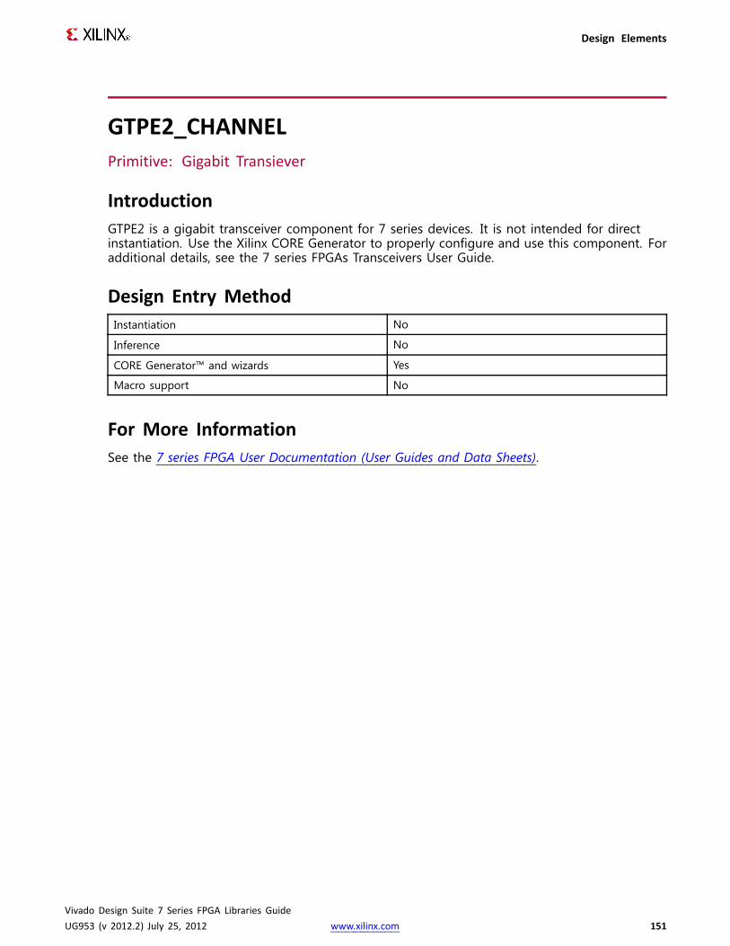
Design Elements
GTPE2_CHANNELPrimitive: Gigabit Transiever
IntroductionGTPE2 is a gigabit transceiver component for 7 series devices. It is not intended for directinstantiation. Use the Xilinx CORE Generator to properly configure and use this component. Foradditional details, see the 7 series FPGAs Transceivers User Guide.
Design Entry MethodInstantiation No
Inference No
CORE Generator™ and wizards Yes
Macro support No
For More InformationSee the 7 series FPGA User Documentation (User Guides and Data Sheets).
Vivado Design Suite 7 Series FPGA Libraries GuideUG953 (v 2012.2) July 25, 2012 www.xilinx.com 151

Design Elements
GTPE2_COMMONPrimitive: Gigabit Transiever
IntroductionGTPE2 is a gigabit transceiver component for 7 series devices. It is not intended for directinstantiation. Use the Xilinx CORE Generator to properly configure and use this component. Foradditional details, see the 7 series FPGAs Transceivers User Guide.
Design Entry MethodInstantiation No
Inference No
CORE Generator™ and wizards Yes
Macro support No
For More InformationSee the 7 series FPGA User Documentation (User Guides and Data Sheets).
Vivado Design Suite 7 Series FPGA Libraries GuideUG953 (v 2012.2) July 25, 2012 www.xilinx.com 152

Design Elements
IBUFPrimitive: Input Buffer
IntroductionThis design element is automatically inserted (inferred) by the synthesis tool to any signaldirectly connected to a top-level input or in-out port of the design. You should generally letthe synthesis tool infer this buffer. However, it can be instantiated into the design if required. Inorder to do so, connect the input port (I) directly to the associated top-level input or in-outport, and connect the output port (O) to the logic sourced by that port. Modify any necessarygeneric maps (VHDL) or named parameter value assignment (Verilog) in order to change thedefault behavior of the component.
Port DescriptionsPort Direction Width Function
O Output 1 Buffer output
I Input 1 Buffer input
Design Entry MethodInstantiation Yes
Inference Recommended
CORE Generator™ and wizards No
Macro support No
In general, this element is inferred by the synthesis tool for any specified top-level input port tothe design. It is generally not necessary to specify them in the source code. However, if desired,they be manually instantiated by either copying the instantiation code from the appropriateLibraries Guide HDL template and pasting it into the top-level entity/module of your code. Itis recommended to always put all I/O components on the top-level of the design to helpfacilitate hierarchical design methods. Connect the I port directly to the top-level input port ofthe design and the O port to the logic in which this input is to source. Specify the desiredgeneric/defparam values in order to configure the proper behavior of the buffer.
Vivado Design Suite 7 Series FPGA Libraries GuideUG953 (v 2012.2) July 25, 2012 www.xilinx.com 153
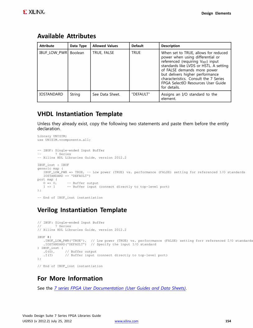
Design Elements
Available AttributesAttribute Data Type Allowed Values Default Description
IBUF_LOW_PWR Boolean TRUE, FALSE TRUE When set to TRUE, allows for reducedpower when using differential orreferenced (requiring VREF) inputstandards like LVDS or HSTL. A settingof FALSE demands more powerbut delivers higher performancecharacteristics. Consult the 7 SeriesFPGA SelectIO Resources User Guidefor details.
IOSTANDARD String See Data Sheet. "DEFAULT" Assigns an I/O standard to theelement.
VHDL Instantiation TemplateUnless they already exist, copy the following two statements and paste them before the entitydeclaration.Library UNISIM;use UNISIM.vcomponents.all;
-- IBUF: Single-ended Input Buffer-- 7 Series-- Xilinx HDL Libraries Guide, version 2012.2
IBUF_inst : IBUFgeneric map (
IBUF_LOW_PWR=> TRUE, -- Low power (TRUE) vs. performance (FALSE) setting for referenced I/O standardsIOSTANDARD=> "DEFAULT")
port map (O => O, -- Buffer outputI => I -- Buffer input (connect directly to top-level port)
);
-- End of IBUF_inst instantiation
Verilog Instantiation Template
// IBUF: Single-ended Input Buffer// 7 Series// Xilinx HDL Libraries Guide, version 2012.2
IBUF #(.IBUF_LOW_PWR("TRUE"), // Low power (TRUE) vs. perforrmance (FALSE) setting forr referenced I/O standards.IOSTANDARD("DEFAULT") // Specify the input I/O standard
) IBUF_inst (.O(O), // Buffer output.I(I) // Buffer input (connect directly to top-level port)
);
// End of IBUF_inst instantiation
For More InformationSee the 7 series FPGA User Documentation (User Guides and Data Sheets).
Vivado Design Suite 7 Series FPGA Libraries GuideUG953 (v 2012.2) July 25, 2012 www.xilinx.com 154

Design Elements
IBUF_IBUFDISABLEPrimitive: Single-ended Input Buffer with Input Disable
IntroductionThis design element is an input buffer used to connect internal logic to an external pin. Thiselement includes an input path disable as an additional power saving feature when the I/Ois not used for a sustained amount of time.
Port DescriptionsPort Direction Width Function
I Input 1 Input port connection.Connect directly totop-level port in thedesign.
IBUFDISABLE Input 1 Disables input paththrough the buffer andforces to a logic highwhen USE_IBUFDISABLEis set to "TRUE" and thissignal is asserted high.If USE_IBUFDISABLE isset to "FALSE" this inputis ignored and shouldbe tied to ground. Thisfeature is generally usedto reduce power at timeswhen the I/O is idle for aperiod of time.
O Output 1 Buffer outputrepresenting the inputpath to the device.
Design Entry MethodInstantiation Yes
Inference No
CORE Generator™ and wizards Yes
Macro support No
Vivado Design Suite 7 Series FPGA Libraries GuideUG953 (v 2012.2) July 25, 2012 www.xilinx.com 155

Design Elements
Available Attributes
AttributeDataType Allowed Values Default Description
IBUF_LOW_PWR String "TRUE","FALSE"
"TRUE" Allows a trade off of lower powerconsumption versus highest performancewhen referenced I/O standards are used.
IOSTANDARD String See DataSheet
"DEFAULT" Assigns an I/O standard to the element.
USE_IBUFDISABLE String "TRUE","FALSE"
"TRUE" Enables or disables the feature ofIBUFDISABLE.
VHDL Instantiation TemplateUnless they already exist, copy the following two statements and paste them before the entitydeclaration.Library UNISIM;use UNISIM.vcomponents.all;
-- IBUF_IBUFDISABLE: Single-ended Input Buffer with Disable-- 7 Series-- Xilinx HDL Libraries Guide, version 2012.2
IBUF_IBUFDISABLE_inst : IBUF_IBUFDISABLEgeneric map (
IBUF_LOW_PWR=> "TRUE", -- Low power (TRUE) vs. performance (FALSE) setting for referenced I/O standardsIOSTANDARD=> "DEFAULT", -- Specify the input I/O standardUSE_IBUFDISABLE => "TRUE") -- Set to "TRUE" to enable IBUFDISABLE feature
port map (O => O, -- Buffer outputI => I, -- Buffer input (connect directly to top-level port)IBUFDISABLE => IBUFDISABLE -- Buffer disable input, low=disable
);
-- End of IBUF_IBUFDISABLE_inst instantiation
Verilog Instantiation Template// IBUF_IBUFDISABLE: Single-ended Input Buffer with Disable// 7 Series// Xilinx HDL Libraries Guide, version 2012.2
IBUF_IBUFDISABLE #(.IBUF_LOW_PWR("TRUE"), // Low power ("TRUE") vs. perforrmance ("FALSE") forr referenced I/O standards.IOSTANDARD("DEFAULT"), // Specify the input I/O standard.USE_IBUFDISABLE("TRUE") // Set to "TRUE" to enable IBUFDISABLE feature
) IBUF_IBUFDISABLE_inst (.O(O), // Buffer output.I(I), // Buffer input (connect directly to top-level port).IBUFDISABLE(IBUFDISABLE) // Buffer disable input, low=disable
);
// End of IBUF_IBUFDISABLE_inst instantiation
For More Information• See the 7 series FPGA SelectIO Resources User Guide (UG471).• See the 7 series FPGA User Documentation (User Guides and Data Sheets).
Vivado Design Suite 7 Series FPGA Libraries GuideUG953 (v 2012.2) July 25, 2012 www.xilinx.com 156
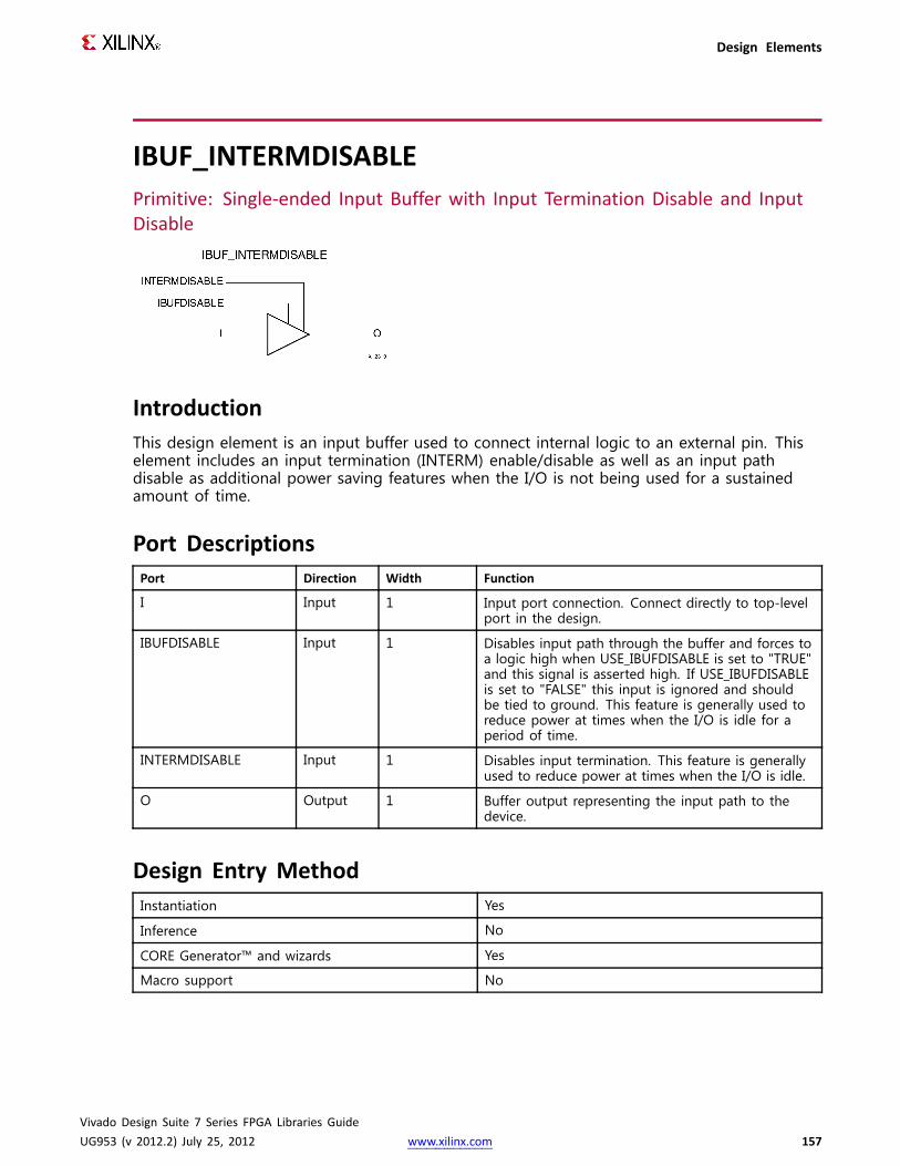
Design Elements
IBUF_INTERMDISABLEPrimitive: Single-ended Input Buffer with Input Termination Disable and InputDisable
IntroductionThis design element is an input buffer used to connect internal logic to an external pin. Thiselement includes an input termination (INTERM) enable/disable as well as an input pathdisable as additional power saving features when the I/O is not being used for a sustainedamount of time.
Port DescriptionsPort Direction Width Function
I Input 1 Input port connection. Connect directly to top-levelport in the design.
IBUFDISABLE Input 1 Disables input path through the buffer and forces toa logic high when USE_IBUFDISABLE is set to "TRUE"and this signal is asserted high. If USE_IBUFDISABLEis set to "FALSE" this input is ignored and shouldbe tied to ground. This feature is generally used toreduce power at times when the I/O is idle for aperiod of time.
INTERMDISABLE Input 1 Disables input termination. This feature is generallyused to reduce power at times when the I/O is idle.
O Output 1 Buffer output representing the input path to thedevice.
Design Entry MethodInstantiation Yes
Inference No
CORE Generator™ and wizards Yes
Macro support No
Vivado Design Suite 7 Series FPGA Libraries GuideUG953 (v 2012.2) July 25, 2012 www.xilinx.com 157

Design Elements
Available Attributes
AttributeDataType Allowed Values Default Description
IBUF_LOW_PWR String "TRUE","FALSE"
"TRUE" Allows a trade off of lower powerconsumption vs. highest performance whenreferenced I/O standards are used.
IOSTANDARD String See DataSheet
"DEFAULT" Assigns an I/O standard to the element.
USE_IBUFDISABLE String "TRUE","FALSE"
"TRUE" Enables or disables the feature ofIBUFDISABLE.
VHDL Instantiation TemplateUnless they already exist, copy the following two statements and paste them before the entitydeclaration.Library UNISIM;use UNISIM.vcomponents.all;
-- IBUF_INTERMDISABLE: Single-ended Input Buffer with Termination Input Disable-- May only be placed in High Range (HR) Banks-- 7 Series-- Xilinx HDL Libraries Guide, version 2012.2
IBUF_INTERMDISABLE_inst : IBUF_INTERMDISABLEgeneric map (
IBUF_LOW_PWR=> "TRUE", -- Low power (TRUE) vs. performance (FALSE) setting for referenced I/O standardsIOSTANDARD=> "DEFAULT", -- Specify the input I/O standardUSE_IBUFDISABLE => "TRUE") -- Set to "TRUE" to enable IBUFDISABLE feature
port map (O => O, -- Buffer outputI => I, -- Buffer input (connect directly to top-level port)INTERMDISABLE => INTERMDISABLE, -- Input Termination DisableIBUFDISABLE => IBUFDISABLE -- Buffer disable input, low=disable
);
-- End of IBUF_INTERMDISABLE_inst instantiation
Verilog Instantiation Template
// IBUF_INTERMDISABLE: Single-ended Input Buffer with Termination Input Disable// May only be placed in High Range (HR) Banks// 7 Series// Xilinx HDL Libraries Guide, version 2012.2
IBUF_INTERMDISABLE #(.IBUF_LOW_PWR("TRUE"), // Low power ("TRUE") vs. perforrmance ("FALSE") forr referenced I/O standards.IOSTANDARD("DEFAULT"), // Specify the input I/O standard.USE_IBUFDISABLE("TRUE") // Set to "TRUE" to enable IBUFDISABLE feature
) IBUF_INTERMDISABLE_inst (.O(O), // Buffer output.I(I), // Buffer input (connect directly to top-level port).IBUFDISABLE(IBUFDISABLE), // Buffer disable input, low=disable.INTERMDISABLE(INTERMDISABLE) // Input Termination Disable
);
// End of IBUF_INTERMDISABLE_inst instantiation
Vivado Design Suite 7 Series FPGA Libraries GuideUG953 (v 2012.2) July 25, 2012 www.xilinx.com 158

Design Elements
For More Information• See the 7 series FPGA SelectIO Resources User Guide (UG471).
• See the 7 series FPGA User Documentation (User Guides and Data Sheets).
Vivado Design Suite 7 Series FPGA Libraries GuideUG953 (v 2012.2) July 25, 2012 www.xilinx.com 159

Design Elements
IBUFDSPrimitive: Differential Signaling Input Buffer
IntroductionThis design element is an input buffer that supports low-voltage, differential signaling. InIBUFDS, a design level interface signal is represented as two distinct ports (I and IB), onedeemed the "master" and the other the "slave." The master and the slave are opposite phasesof the same logical signal (for example, MYNET_P and MYNET_N). Optionally, a programmabledifferential termination feature is available to help improve signal integrity and reduce externalcomponents.
Logic TableInputs Outputs
I IB O
0 0 No Change
0 1 0
1 0 1
1 1 No Change
Port DescriptionsPort Direction Width Function
I Input 1 Diff_p Buffer Input
IB Input 1 Diff_n Buffer Input
O Output 1 Buffer Output
Design Entry MethodInstantiation Recommended
Inference No
CORE Generator™ and wizards No
Macro support No
Vivado Design Suite 7 Series FPGA Libraries GuideUG953 (v 2012.2) July 25, 2012 www.xilinx.com 160

Design Elements
Put all I/O components on the top-level of the design to help facilitate hierarchical designmethods. Connect the I port directly to the top-level "master" input port of the design, theIB port to the top-level "slave" input port, and the O port to the logic in which this inputis to source. Specify the desired generic/defparam values in order to configure the properbehavior of the buffer.
Available Attributes
AttributeDataType Allowed Values Default Description
DIFF_TERM Boolean TRUE, FALSE FALSE The differential termination attribute isdesigned for the 7 Series FPGA supporteddifferential input I/O standards. It is used toturn the built-in differential termination on(TRUE) or off (FALSE).
IBUF_LOW_PWR Boolean TRUE, FALSE TRUE When set to TRUE, allows for reducedpower when using differential or referenced(requiring VREF) input standards like LVDSor HSTL. A setting of FALSE demands morepower but delivers higher performancecharacteristics. Consult the 7 Series FPGASelectIO Resources User Guide for details.
IOSTANDARD String See DataSheet.
"DEFAULT" Assigns an I/O standard to the element.
VHDL Instantiation TemplateUnless they already exist, copy the following two statements and paste them before the entitydeclaration.Library UNISIM;use UNISIM.vcomponents.all;
-- IBUFDS: Differential Input Buffer-- 7 Series-- Xilinx HDL Libraries Guide, version 2012.2
IBUFDS_inst : IBUFDSgeneric map (
DIFF_TERM => FALSE, -- Differential TerminationIBUF_LOW_PWR=> TRUE, -- Low power (TRUE) vs. performance (FALSE) setting for referenced I/O standardsIOSTANDARD=> "DEFAULT")
port map (O => O, -- Buffer outputI => I, -- Diff_p buffer input (connect directly to top-level port)IB => IB -- Diff_n buffer input (connect directly to top-level port)
);
-- End of IBUFDS_inst instantiation
Vivado Design Suite 7 Series FPGA Libraries GuideUG953 (v 2012.2) July 25, 2012 www.xilinx.com 161
Design Elements
Verilog Instantiation Template
// IBUFDS: Differential Input Buffer// 7 Series// Xilinx HDL Libraries Guide, version 2012.2
IBUFDS #(.DIFF_TERM("FALSE"), // Differential Termination.IBUF_LOW_PWR("TRUE"), // Low power="TRUE", Highest perforrmance="FALSE".IOSTANDARD("DEFAULT") // Specify the input I/O standard
) IBUFDS_inst (.O(O), // Buffer output.I(I), // Diff_p buffer input (connect directly to top-level port).IB(IB) // Diff_n buffer input (connect directly to top-level port)
);
// End of IBUFDS_inst instantiation
For More InformationSee the 7 series FPGA User Documentation (User Guides and Data Sheets).
Vivado Design Suite 7 Series FPGA Libraries GuideUG953 (v 2012.2) July 25, 2012 www.xilinx.com 162
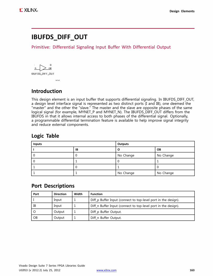
Design Elements
IBUFDS_DIFF_OUTPrimitive: Differential Signaling Input Buffer With Differential Output
IntroductionThis design element is an input buffer that supports differential signaling. In IBUFDS_DIFF_OUT,a design level interface signal is represented as two distinct ports (I and IB), one deemed the"master" and the other the "slave." The master and the slave are opposite phases of the samelogical signal (for example, MYNET_P and MYNET_N). The IBUFDS_DIFF_OUT differs from theIBUFDS in that it allows internal access to both phases of the differential signal. Optionally,a programmable differential termination feature is available to help improve signal integrityand reduce external components.
Logic TableInputs Outputs
I IB O OB
0 0 No Change No Change
0 1 0 1
1 0 1 0
1 1 No Change No Change
Port DescriptionsPort Direction Width Function
I Input 1 Diff_p Buffer Input (connect to top-level port in the design).
IB Input 1 Diff_n Buffer Input (connect to top-level port in the design).
O Output 1 Diff_p Buffer Output.
OB Output 1 Diff_n Buffer Output.
Vivado Design Suite 7 Series FPGA Libraries GuideUG953 (v 2012.2) July 25, 2012 www.xilinx.com 163

Design Elements
Design Entry MethodInstantiation Recommended
Inference No
CORE Generator™ and wizards No
Macro support No
It is suggested to put all I/O components on the top-level of the design to help facilitatehierarchical design methods. Connect the I port directly to the top-level "master" input portof the design, the IB port to the top-level "slave" input port, and the O and OB ports to thelogic in which this input is to source. Specify the desired generic/parameter values in order toconfigure the proper behavior of the buffer.
Available Attributes
AttributeDataType Allowed Values Default Description
DIFF_TERM Boolean TRUE, FALSE FALSE The differential termination attribute isdesigned for the 7 Series FPGA supporteddifferential input I/O standards. It is used toturn the built-in differential termination on(TRUE) or off (FALSE).
IBUF_LOW_PWR Boolean TRUE, FALSE TRUE When set to TRUE, allows for reducedpower when using differential or referenced(requiring VREF) input standards like LVDSor HSTL. A setting of FALSE demands morepower but delivers higher performancecharacteristics. Consult the 7 Series FPGASelectIO Resources User Guide for details.
IOSTANDARD String See DataSheet.
"DEFAULT" Assigns an I/O standard to the element.
VHDL Instantiation TemplateUnless they already exist, copy the following two statements and paste them before the entitydeclaration.Library UNISIM;use UNISIM.vcomponents.all;
-- IBUFDS_DIFF_OUT: Differential Input Buffer with Differential Output-- 7 Series-- Xilinx HDL Libraries Guide, version 2012.2
IBUFDS_DIFF_OUT_inst : IBUFDS_DIFF_OUTgeneric map (
DIFF_TERM => FALSE, -- Differential TerminationIBUF_LOW_PWR=> TRUE, -- Low power (TRUE) vs. performance (FALSE) setting for referenced I/O standardsIOSTANDARD=> "DEFAULT", -- Specify the input I/O standardUSE_IBUFDISABLE => "TRUE"
port map (O => O, -- Buffer diff_p outputOB => OB, -- Buffer diff_n outputI => I, -- Diff_p buffer input (connect directly to top-level port)IB => IB -- Diff_n buffer input (connect directly to top-level port)
);
Vivado Design Suite 7 Series FPGA Libraries GuideUG953 (v 2012.2) July 25, 2012 www.xilinx.com 164

Design Elements
-- End of IBUFDS_DIFF_OUT_inst instantiation
Verilog Instantiation Template
// IBUFDS_DIFF_OUT: Differential Input Buffer with Differential Output// 7 Series// Xilinx HDL Libraries Guide, version 2012.2
IBUFDS_DIFF_OUT #(.DIFF_TERM("FALSE"), // Differential Termination, "TRUE"/"FALSE".IBUF_LOW_PWR("TRUE"), // Low power="TRUE", Highest perforrmance="FALSE".IOSTANDARD("DEFAULT") // Specify the input I/O standard
) IBUFDS_DIFF_OUT_inst (.O(O), // Buffer diff_p output.OB(OB), // Buffer diff_n output.I(I), // Diff_p buffer input (connect directly to top-level port).IB(IB) // Diff_n buffer input (connect directly to top-level port)
);
// End of IBUFDS_DIFF_OUT_inst instantiation
For More Information• See the 7 series FPGA SelectIO Resources User Guide (UG471).
• See the 7 series FPGA User Documentation (User Guides and Data Sheets).
Vivado Design Suite 7 Series FPGA Libraries GuideUG953 (v 2012.2) July 25, 2012 www.xilinx.com 165

Design Elements
IBUFDS_DIFF_OUT_IBUFDISABLEPrimitive: Input Differential Buffer with Input Disable and Differential Output
IntroductionThis design element is a differential input buffer used to connect internal logic to an externalbidirectional pin. This element includes an input path disable as an additional power savingfeature when the input is idle for a sustained time. The IOBUFDS_DIFF_OUT_IBUFDISABLEdiffers from the IOBUFDS_IBUFDISABLE in that it allows internal access to both phases ofthe differential signal.
Port DescriptionsPort Direction Width Function
I Input 1 Input p-side portconnection. Connectdirectly to top-level portin the design.
IB Input 1 Input n-side portconnection. Connectdirectly to top-level portin the design.
IBUFDISABLE Input 1 Disables input paththrough the buffer andforces to a logic highwhen USE_IBUFDISABLEis set to "TRUE" and thissignal is asserted high.If USE_IBUFDISABLE isset to "FALSE" this inputis ignored and shouldbe tied to ground. Thisfeature is generally usedto reduce power at timeswhen the I/O is idle for aperiod of time.
O Output 1 Buffer p-side outputrepresenting the inputpath to the device.
OB Output 1 Buffer n-side outputrepresenting the inputpath to the device.
Vivado Design Suite 7 Series FPGA Libraries GuideUG953 (v 2012.2) July 25, 2012 www.xilinx.com 166

Design Elements
Design Entry MethodInstantiation Yes
Inference No
CORE Generator™ and wizards Yes
Macro support No
Available Attributes
AttributeDataType Allowed Values Default Description
DIFF_TERM String "TRUE","FALSE"
"FALSE" Enable the built-in differential termination.
IBUF_LOW_PWR String "TRUE","FALSE"
"TRUE" Allows a trade off of lower powerconsumption vs. highest performance whenreferenced I/O standards are used.
IOSTANDARD String See DataSheet
"DEFAULT" Assigns an I/O standard to the element.
USE_IBUFDISABLE String "TRUE","FALSE"
"TRUE" Enables or disables the feature ofIBUFDISABLE.
VHDL Instantiation TemplateUnless they already exist, copy the following two statements and paste them before the entitydeclaration.Library UNISIM;use UNISIM.vcomponents.all;
-- IBUFDS_DIFF_OUT_IBUFDISABLE: Differential Input Buffer with Differential Output w/ Disable-- 7 Series-- Xilinx HDL Libraries Guide, version 2012.2
IBUFDS_DIFF_OUT_IBUFDISABLE_inst : IBUFDS_DIFF_OUT_IBUFDISABLEgeneric map (
DIFF_TERM => "FALSE", -- Differential TerminationIBUF_LOW_PWR=> "TRUE", -- Low power "TRUE" vs. performance "FALSE" setting for referenced I/O standardsIOSTANDARD=> "DEFAULT", -- Specify the input I/O standardUSE_IBUFDISABLE => "TRUE") -- Set to "TRUE" to enable IBUFDISABLE feature
port map (O => O, -- Buffer diff_p outputOB => OB, -- Buffer diff_n outputI => I, -- Diff_p buffer input (connect directly to top-level port)IB => IB, -- Diff_n buffer input (connect directly to top-level port)IBUFDISABLE => IBUFDISABLE -- Buffer disable input, low=disable
);
-- End of IBUFDS_DIFF_OUT_IBUFDISABLE_inst instantiation
Vivado Design Suite 7 Series FPGA Libraries GuideUG953 (v 2012.2) July 25, 2012 www.xilinx.com 167

Design Elements
Verilog Instantiation Template
// IBUFDS_DIFF_OUT_IBUFDISABLE: Differential Input Buffer with Differential Output with Input Disable// 7 Series// Xilinx HDL Libraries Guide, version 2012.2
IBUFDS_DIFF_OUT_IBUFDISABLE #(.DIFF_TERM("FALSE"), // Differential Termination, "TRUE"/"FALSE".IBUF_LOW_PWR("TRUE"), // Low power="TRUE", Highest perforrmance="FALSE".IOSTANDARD("DEFAULT"), // Specify the input I/O standard.USE_IBUFDISABLE("TRUE") // Set to "TRUE" to enable IBUFDISABLE feature
) IBUFDS_DIFF_OUT_IBUFDISABLE_inst (.O(O), // Buffer diff_p output.OB(OB), // Buffer diff_n output.I(I), // Diff_p buffer input (connect directly to top-level port).IB(IB), // Diff_n buffer input (connect directly to top-level port).IBUFDISABLE(IBUFDISABLE) // Buffer disable input, low=disable
);
// End of IBUFDS_DIFF_OUT_IBUFDISABLE_inst instantiation
For More Information• See the 7 series FPGA SelectIO Resources User Guide (UG471).
• See the 7 series FPGA User Documentation (User Guides and Data Sheets).
Vivado Design Suite 7 Series FPGA Libraries GuideUG953 (v 2012.2) July 25, 2012 www.xilinx.com 168
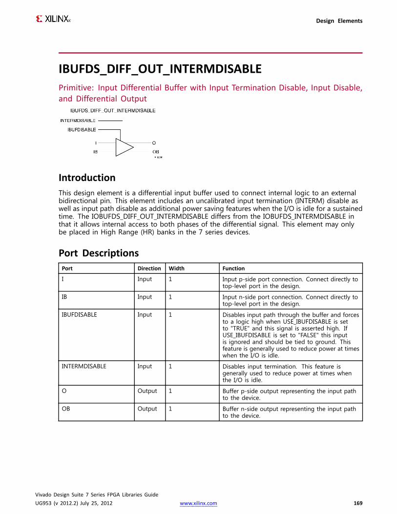
Design Elements
IBUFDS_DIFF_OUT_INTERMDISABLEPrimitive: Input Differential Buffer with Input Termination Disable, Input Disable,and Differential Output
IntroductionThis design element is a differential input buffer used to connect internal logic to an externalbidirectional pin. This element includes an uncalibrated input termination (INTERM) disable aswell as input path disable as additional power saving features when the I/O is idle for a sustainedtime. The IOBUFDS_DIFF_OUT_INTERMDISABLE differs from the IOBUFDS_INTERMDISABLE inthat it allows internal access to both phases of the differential signal. This element may onlybe placed in High Range (HR) banks in the 7 series devices.
Port DescriptionsPort Direction Width Function
I Input 1 Input p-side port connection. Connect directly totop-level port in the design.
IB Input 1 Input n-side port connection. Connect directly totop-level port in the design.
IBUFDISABLE Input 1 Disables input path through the buffer and forcesto a logic high when USE_IBUFDISABLE is setto "TRUE" and this signal is asserted high. IfUSE_IBUFDISABLE is set to "FALSE" this inputis ignored and should be tied to ground. Thisfeature is generally used to reduce power at timeswhen the I/O is idle.
INTERMDISABLE Input 1 Disables input termination. This feature isgenerally used to reduce power at times whenthe I/O is idle.
O Output 1 Buffer p-side output representing the input pathto the device.
OB Output 1 Buffer n-side output representing the input pathto the device.
Vivado Design Suite 7 Series FPGA Libraries GuideUG953 (v 2012.2) July 25, 2012 www.xilinx.com 169

Design Elements
Design Entry MethodInstantiation Yes
Inference No
CORE Generator™ and wizards Yes
Macro support No
Available Attributes
AttributeDataType Allowed Values Default Description
DIFF_TERM String "TRUE","FALSE"
"FALSE" Enable the built-in differential termination.
IBUF_LOW_PWR String "TRUE","FALSE"
"TRUE" Allows a trade off of lower powerconsumption vs. highest performance whenreferenced I/O standards are used.
IOSTANDARD String See DataSheet
"DEFAULT" Assigns an I/O standard to the element.
USE_IBUFDISABLE String "TRUE","FALSE"
"TRUE" Enables or disables the feature ofIBUFDISABLE.
VHDL Instantiation TemplateUnless they already exist, copy the following two statements and paste them before the entitydeclaration.Library UNISIM;use UNISIM.vcomponents.all;
-- IBUFDS_DIFF_OUT_INTERMDISABLE: Differential Input Buffer with Differential Output w/ Disable-- 7 Series-- Xilinx HDL Libraries Guide, version 2012.2
IBUFDS_DIFF_OUT_INTERMDISABLE_inst : IBUFDS_DIFF_OUT_INTERMDISABLEgeneric map (
DIFF_TERM => "FALSE", -- Differential TerminationIBUF_LOW_PWR=> "TRUE", -- Low power "TRUE" vs. performance "FALSE" setting for referenced I/O standardsIOSTANDARD=> "DEFAULT", -- Specify the input I/O standardUSE_IBUFDISABLE => "TRUE") -- Set to "TRUE" to enable IBUFDISABLE feature
port map (O => O, -- Buffer diff_p outputOB => OB, -- Buffer diff_n outputI => I, -- Diff_p buffer input (connect directly to top-level port)IB => IB, -- Diff_n buffer input (connect directly to top-level port)IBUFDISABLE => IBUFDISABLE, -- Buffer disable input, low=disableINTERMDISABLE => INTERMDISABLE -- Input termination disable
);
-- End of IBUFDS_DIFF_OUT_INTERMDISABLE_inst instantiation
Vivado Design Suite 7 Series FPGA Libraries GuideUG953 (v 2012.2) July 25, 2012 www.xilinx.com 170
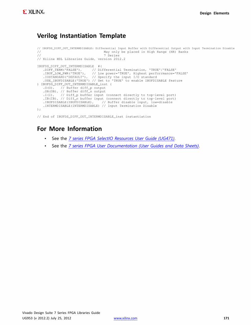
Design Elements
Verilog Instantiation Template
// IBUFDS_DIFF_OUT_INTERMDISABLE: Differential Input Buffer with Differential Output with Input Termination Disable// May only be placed in High Range (HR) Banks// 7 Series// Xilinx HDL Libraries Guide, version 2012.2
IBUFDS_DIFF_OUT_INTERMDISABLE #(.DIFF_TERM("FALSE"), // Differential Termination, "TRUE"/"FALSE".IBUF_LOW_PWR("TRUE"), // Low power="TRUE", Highest perforrmance="FALSE".IOSTANDARD("DEFAULT"), // Specify the input I/O standard.USE_IBUFDISABLE("TRUE") // Set to "TRUE" to enable IBUFDISABLE feature
) IBUFDS_DIFF_OUT_INTERMDISABLE_inst (.O(O), // Buffer diff_p output.OB(OB), // Buffer diff_n output.I(I), // Diff_p buffer input (connect directly to top-level port).IB(IB), // Diff_n buffer input (connect directly to top-level port).IBUFDISABLE(IBUFDISABLE), // Buffer disable input, low=disable.INTERMDISABLE(INTERMDISABLE) // Input Termination Disable
);
// End of IBUFDS_DIFF_OUT_INTERMDISABLE_inst instantiation
For More Information• See the 7 series FPGA SelectIO Resources User Guide (UG471).
• See the 7 series FPGA User Documentation (User Guides and Data Sheets).
Vivado Design Suite 7 Series FPGA Libraries GuideUG953 (v 2012.2) July 25, 2012 www.xilinx.com 171
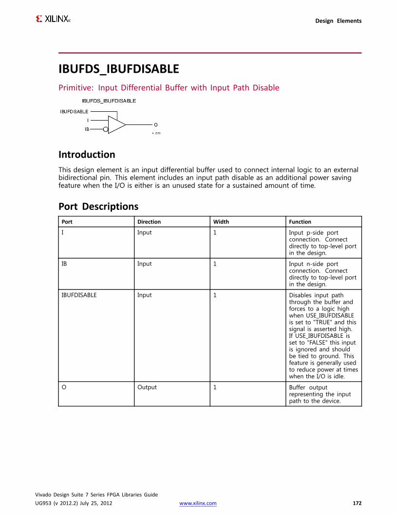
Design Elements
IBUFDS_IBUFDISABLEPrimitive: Input Differential Buffer with Input Path Disable
IntroductionThis design element is an input differential buffer used to connect internal logic to an externalbidirectional pin. This element includes an input path disable as an additional power savingfeature when the I/O is either is an unused state for a sustained amount of time.
Port DescriptionsPort Direction Width Function
I Input 1 Input p-side portconnection. Connectdirectly to top-level portin the design.
IB Input 1 Input n-side portconnection. Connectdirectly to top-level portin the design.
IBUFDISABLE Input 1 Disables input paththrough the buffer andforces to a logic highwhen USE_IBUFDISABLEis set to "TRUE" and thissignal is asserted high.If USE_IBUFDISABLE isset to "FALSE" this inputis ignored and shouldbe tied to ground. Thisfeature is generally usedto reduce power at timeswhen the I/O is idle.
O Output 1 Buffer outputrepresenting the inputpath to the device.
Vivado Design Suite 7 Series FPGA Libraries GuideUG953 (v 2012.2) July 25, 2012 www.xilinx.com 172
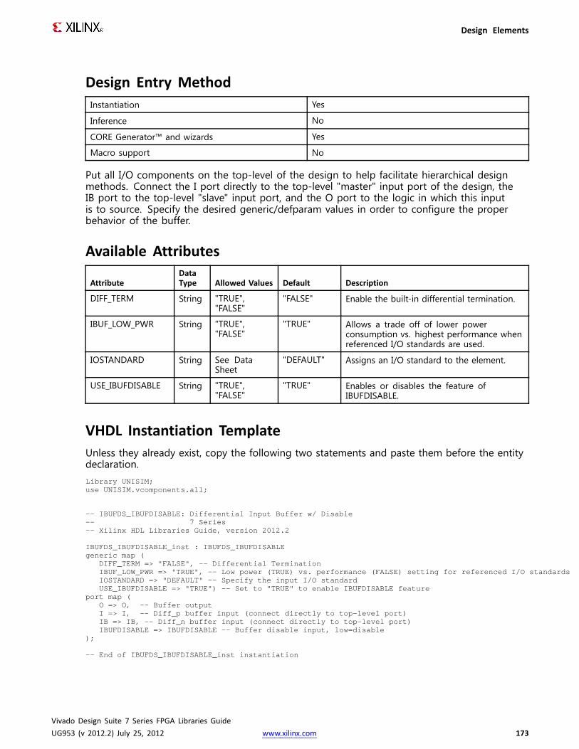
Design Elements
Design Entry MethodInstantiation Yes
Inference No
CORE Generator™ and wizards Yes
Macro support No
Put all I/O components on the top-level of the design to help facilitate hierarchical designmethods. Connect the I port directly to the top-level "master" input port of the design, theIB port to the top-level "slave" input port, and the O port to the logic in which this inputis to source. Specify the desired generic/defparam values in order to configure the properbehavior of the buffer.
Available Attributes
AttributeDataType Allowed Values Default Description
DIFF_TERM String "TRUE","FALSE"
"FALSE" Enable the built-in differential termination.
IBUF_LOW_PWR String "TRUE","FALSE"
"TRUE" Allows a trade off of lower powerconsumption vs. highest performance whenreferenced I/O standards are used.
IOSTANDARD String See DataSheet
"DEFAULT" Assigns an I/O standard to the element.
USE_IBUFDISABLE String "TRUE","FALSE"
"TRUE" Enables or disables the feature ofIBUFDISABLE.
VHDL Instantiation TemplateUnless they already exist, copy the following two statements and paste them before the entitydeclaration.Library UNISIM;use UNISIM.vcomponents.all;
-- IBUFDS_IBUFDISABLE: Differential Input Buffer w/ Disable-- 7 Series-- Xilinx HDL Libraries Guide, version 2012.2
IBUFDS_IBUFDISABLE_inst : IBUFDS_IBUFDISABLEgeneric map (
DIFF_TERM => "FALSE", -- Differential TerminationIBUF_LOW_PWR=> "TRUE", -- Low power (TRUE) vs. performance (FALSE) setting for referenced I/O standardsIOSTANDARD=> "DEFAULT" -- Specify the input I/O standardUSE_IBUFDISABLE => "TRUE") -- Set to "TRUE" to enable IBUFDISABLE feature
port map (O => O, -- Buffer outputI => I, -- Diff_p buffer input (connect directly to top-level port)IB => IB, -- Diff_n buffer input (connect directly to top-level port)IBUFDISABLE => IBUFDISABLE -- Buffer disable input, low=disable
);
-- End of IBUFDS_IBUFDISABLE_inst instantiation
Vivado Design Suite 7 Series FPGA Libraries GuideUG953 (v 2012.2) July 25, 2012 www.xilinx.com 173

Design Elements
Verilog Instantiation Template
// IBUFDS_IBUFDISABLE: Differential Input Buffer with Input Disable// 7 Series// Xilinx HDL Libraries Guide, version 2012.2
IBUFDS_IBUFDISABLE #(.DIFF_TERM("FALSE"), // Differential Termination.IBUF_LOW_PWR("TRUE"), // Low power="TRUE", Highest perforrmance="FALSE".IOSTANDARD("DEFAULT"), // Specify the input I/O standard.USE_IBUFDISABLE("TRUE") // Set to "TRUE" to enable IBUFDISABLE feature
) IBUFDS_IBUFDISABLE_inst (.O(O), // Buffer output.I(I), // Diff_p buffer input (connect directly to top-level port).IB(IB), // Diff_n buffer input (connect directly to top-level port).IBUFDISABLE(IBUFDISABLE) // Buffer disable input, low=disable
);
// End of IBUFDS_IBUFDISABLE_inst instantiation
For More Information• See the 7 series FPGA SelectIO Resources User Guide (UG471).
• See the 7 series FPGA User Documentation (User Guides and Data Sheets).
Vivado Design Suite 7 Series FPGA Libraries GuideUG953 (v 2012.2) July 25, 2012 www.xilinx.com 174

Design Elements
IBUFDS_INTERMDISABLEPrimitive: Input Differential Buffer with Input Termination Disable and InputDisable
IntroductionThis design element is an input differential buffer used to connect internal logic to an externalbidirectional pin. This element includes an uncalibrated input termination (INTERM) disableas well as input path disable as additional power saving features when the input is idle for asustained amount of time. This element may only be placed in High Range (HR) banks inthe 7 series devices.
Port DescriptionsPort Direction Width Function
I Input 1 Input p-side portconnection. Connectdirectly to top-level portin the design.
IB Input 1 Input n-side portconnection. Connectdirectly to top-level portin the design.
IBUFDISABLE Input 1 Disables input paththrough the buffer andforces to a logic highwhen USE_IBUFDISABLEis set to "TRUE" and thissignal is asserted high.If USE_IBUFDISABLE isset to "FALSE" this inputis ignored and shouldbe tied to ground. Thisfeature is generally usedto reduce power at timeswhen the I/O is idle.
INTERMDISABLE Input 1 Disables inputtermination. This featureis generally used toreduce power at timeswhen the I/O is idle.
Vivado Design Suite 7 Series FPGA Libraries GuideUG953 (v 2012.2) July 25, 2012 www.xilinx.com 175
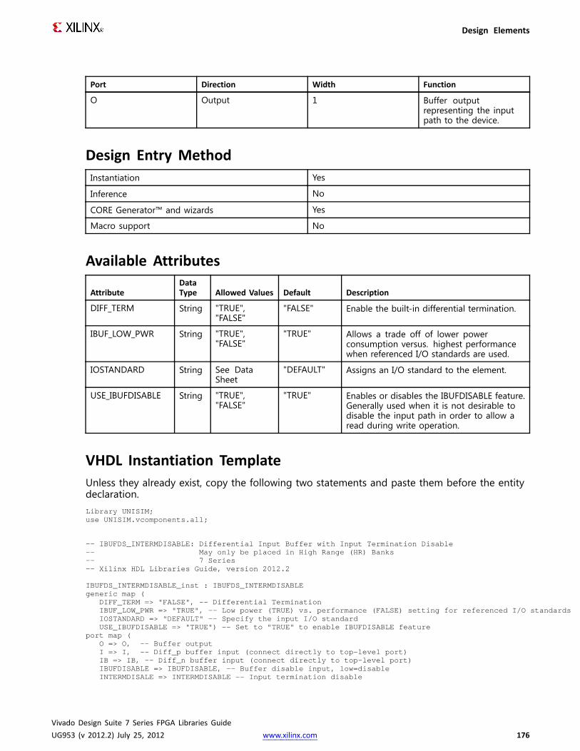
Design Elements
Port Direction Width Function
O Output 1 Buffer outputrepresenting the inputpath to the device.
Design Entry MethodInstantiation Yes
Inference No
CORE Generator™ and wizards Yes
Macro support No
Available Attributes
AttributeDataType Allowed Values Default Description
DIFF_TERM String "TRUE","FALSE"
"FALSE" Enable the built-in differential termination.
IBUF_LOW_PWR String "TRUE","FALSE"
"TRUE" Allows a trade off of lower powerconsumption versus. highest performancewhen referenced I/O standards are used.
IOSTANDARD String See DataSheet
"DEFAULT" Assigns an I/O standard to the element.
USE_IBUFDISABLE String "TRUE","FALSE"
"TRUE" Enables or disables the IBUFDISABLE feature.Generally used when it is not desirable todisable the input path in order to allow aread during write operation.
VHDL Instantiation TemplateUnless they already exist, copy the following two statements and paste them before the entitydeclaration.Library UNISIM;use UNISIM.vcomponents.all;
-- IBUFDS_INTERMDISABLE: Differential Input Buffer with Input Termination Disable-- May only be placed in High Range (HR) Banks-- 7 Series-- Xilinx HDL Libraries Guide, version 2012.2
IBUFDS_INTERMDISABLE_inst : IBUFDS_INTERMDISABLEgeneric map (
DIFF_TERM => "FALSE", -- Differential TerminationIBUF_LOW_PWR=> "TRUE", -- Low power (TRUE) vs. performance (FALSE) setting for referenced I/O standardsIOSTANDARD=> "DEFAULT" -- Specify the input I/O standardUSE_IBUFDISABLE => "TRUE") -- Set to "TRUE" to enable IBUFDISABLE feature
port map (O => O, -- Buffer outputI => I, -- Diff_p buffer input (connect directly to top-level port)IB => IB, -- Diff_n buffer input (connect directly to top-level port)IBUFDISABLE => IBUFDISABLE, -- Buffer disable input, low=disableINTERMDISALE => INTERMDISABLE -- Input termination disable
Vivado Design Suite 7 Series FPGA Libraries GuideUG953 (v 2012.2) July 25, 2012 www.xilinx.com 176
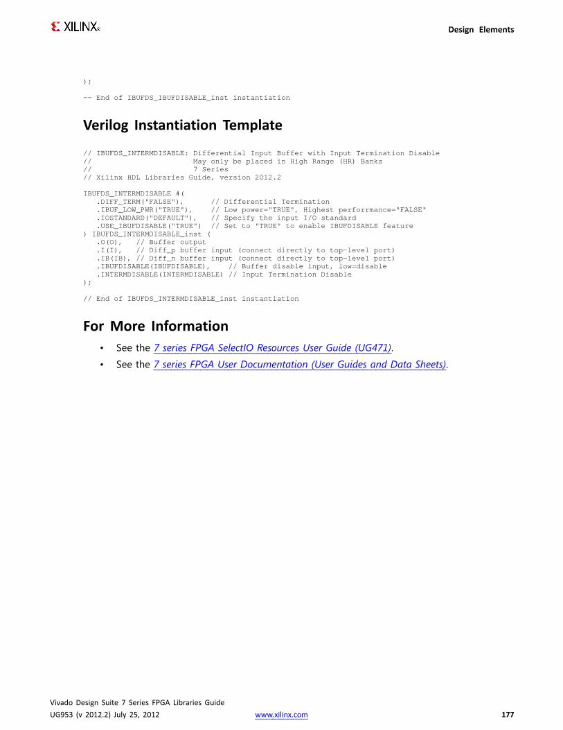
Design Elements
);
-- End of IBUFDS_IBUFDISABLE_inst instantiation
Verilog Instantiation Template
// IBUFDS_INTERMDISABLE: Differential Input Buffer with Input Termination Disable// May only be placed in High Range (HR) Banks// 7 Series// Xilinx HDL Libraries Guide, version 2012.2
IBUFDS_INTERMDISABLE #(.DIFF_TERM("FALSE"), // Differential Termination.IBUF_LOW_PWR("TRUE"), // Low power="TRUE", Highest perforrmance="FALSE".IOSTANDARD("DEFAULT"), // Specify the input I/O standard.USE_IBUFDISABLE("TRUE") // Set to "TRUE" to enable IBUFDISABLE feature
) IBUFDS_INTERMDISABLE_inst (.O(O), // Buffer output.I(I), // Diff_p buffer input (connect directly to top-level port).IB(IB), // Diff_n buffer input (connect directly to top-level port).IBUFDISABLE(IBUFDISABLE), // Buffer disable input, low=disable.INTERMDISABLE(INTERMDISABLE) // Input Termination Disable
);
// End of IBUFDS_INTERMDISABLE_inst instantiation
For More Information• See the 7 series FPGA SelectIO Resources User Guide (UG471).
• See the 7 series FPGA User Documentation (User Guides and Data Sheets).
Vivado Design Suite 7 Series FPGA Libraries GuideUG953 (v 2012.2) July 25, 2012 www.xilinx.com 177

Design Elements
ICAPE2Primitive: Internal Configuration Access Port
IntroductionThis design element gives you access to the configuration functions of the FPGA from theFPGA fabric. Using this component, commands and data can be written to and read from theconfiguration logic of the FPGA array. Since the improper use of this function can have anegative effect on the functionality and reliability of the FPGA, you should not use this elementunless you are very familiar with its capabilities.
Port DescriptionsPort Type Width Function
CLK Input 1 Clock Input
CSIB Input 1 Active-Low ICAP Enable
I<31:0> Input 32 Configuration data input bus
O<31:0> Output 32 Configuration data output bus
RDWRB Input 1 Read/Write Select input
Design Entry MethodInstantiation Recommended
Inference No
CORE Generator™ and wizards No
Macro support No
Vivado Design Suite 7 Series FPGA Libraries GuideUG953 (v 2012.2) July 25, 2012 www.xilinx.com 178

Design Elements
Available AttributesAttribute Type Allowed Values Default Description
DEVICE_ID HEX 32'h03651093,32'h036A2093,32'h036A4093,32'h036A6093,32'h036BF093,32'h036B1093,32'h036B3093,32'h036C2093,32'h036C4093,32'h036C6093,32'h036DF093,32'h036D1093,32'h036D3093,32'h036D5093,32'h036D9093,32'h0362C093,32'h0362D093,32'h0363B093,32'h0364C093,32'h0371F093,32'h0372C093,32'h0377F093,32'h03627093,32'h03628093,32'h03631093,32'h03636093,32'h03642093,32'h03647093,32'h03656093,32'h03667093,32'h03671093,32'h03676093,32'h03680093,32'h03681093,32'h03682093,32'h03687093,32'h03691093,32'h03692093,32'h03696093,32'h03702093,32'h03704093,32'h03711093,32'h03722093,32'h03727093,32'h03731093,32'h03747093,32'h03751093,32'h03752093,32'h03762093,32'h03771093,32'h03782093
0'h3651093 Specifies the pre-programmedDevice ID value to be used forsimulation purposes.
ICAP_WIDTH STRING "X32", "X8", "X16" "X32" Specifies the input and outputdata width.
SIM_CFG_FILE_NAME
STRING "0", "bit", "STRING" "NONE" Specifies the Raw Bitstream (RBT)file to be parsed by the simulationmodel.
Vivado Design Suite 7 Series FPGA Libraries GuideUG953 (v 2012.2) July 25, 2012 www.xilinx.com 179
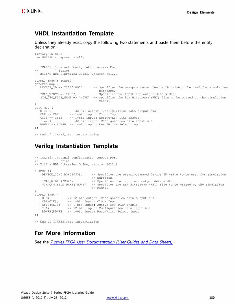
Design Elements
VHDL Instantiation TemplateUnless they already exist, copy the following two statements and paste them before the entitydeclaration.Library UNISIM;use UNISIM.vcomponents.all;
-- ICAPE2: Internal Configuration Access Port-- 7 Series-- Xilinx HDL Libraries Guide, version 2012.2
ICAPE2_inst : ICAPE2generic map (
DEVICE_ID => X"3651093", -- Specifies the pre-programmed Device ID value to be used for simulation-- purposes.
ICAP_WIDTH => "X32", -- Specifies the input and output data width.SIM_CFG_FILE_NAME => "NONE" -- Specifies the Raw Bitstream (RBT) file to be parsed by the simulation
-- model.)port map (
O => O, -- 32-bit output: Configuration data output busCLK => CLK, -- 1-bit input: Clock InputCSIB => CSIB, -- 1-bit input: Active-Low ICAP EnableI => I, -- 32-bit input: Configuration data input busRDWRB=> RDWRB -- 1-bit input: Read/Write Select input
);
-- End of ICAPE2_inst instantiation
Verilog Instantiation Template
// ICAPE2: Internal Configuration Access Port// 7 Series// Xilinx HDL Libraries Guide, version 2012.2
ICAPE2 #(.DEVICE_ID(0'h3651093), // Specifies the pre-programmed Device ID value to be used for simulation
// purposes..ICAP_WIDTH("X32"), // Specifies the input and output data width..SIM_CFG_FILE_NAME("NONE") // Specifies the Raw Bitstream (RBT) file to be parsed by the simulation
// model.)ICAPE2_inst (
.O(O), // 32-bit output: Configuration data output bus
.CLK(CLK), // 1-bit input: Clock Input
.CSIB(CSIB), // 1-bit input: Active-Low ICAP Enable
.I(I), // 32-bit input: Configuration data input bus
.RDWRB(RDWRB) // 1-bit input: Read/Write Select input);
// End of ICAPE2_inst instantiation
For More InformationSee the 7 series FPGA User Documentation (User Guides and Data Sheets).
Vivado Design Suite 7 Series FPGA Libraries GuideUG953 (v 2012.2) July 25, 2012 www.xilinx.com 180

Design Elements
IDDRPrimitive: Input Dual Data-Rate Register
IntroductionThis design element is a dedicated input register designed to receive external dual data rate(DDR) signals into Xilinx® FPGAs. The IDDR is available with modes that present the data tothe FPGA fabric at the time and clock edge they are captured, or on the same clock edge. Thisfeature allows you to avoid additional timing complexities and resource usage.
• OPPOSITE_EDGE mode: Data is recovered in the classic DDR methodology. Given aDDR data and clock at pin D and C respectively, Q1 changes after every positive edge ofclock C, and Q2 changes after every negative edge of clock C.
• SAME_EDGE mode: Data is still recovered by opposite edges of clock C. However, anextra register has been placed in front of the negative edge data register. This extraregister is clocked with positive clock edge of clock signal C. As a result, DDR data isnow presented into the FPGA fabric at the same clock edge. However, because ofthis feature, the data pair appears to be "separated." Q1 and Q2 no longer have pair1 and 2. Instead, the first pair presented is Pair 1 and DONT_CARE, followed by Pair2 and 3 at the next clock cycle.
• SAME_EDGE_PIPELINED mode: Recovers data in a similar fashion as the SAME_EDGEmode. In order to avoid the "separated" effect of the SAME_EDGE mode, an extraregister has been placed in front of the positive edge data register. A data pair nowappears at the Q1 and Q2 pin at the same time. However, using this mode costs you anadditional cycle of latency for Q1 and Q2 signals to change.
IDDR also works with the SelectIO™ features, such as the IODELAYE2.
Note For high speed interfaces, the IDDR_2CLK component can be used to specify twoindependent clocks to capture the data. Use this component when the performancerequirements of the IDDR are not adequate, since the IDDR_2CLK requires more clockingresources and can imply placement restrictions that are not necessary when using the IDDRcomponent.
Vivado Design Suite 7 Series FPGA Libraries GuideUG953 (v 2012.2) July 25, 2012 www.xilinx.com 181
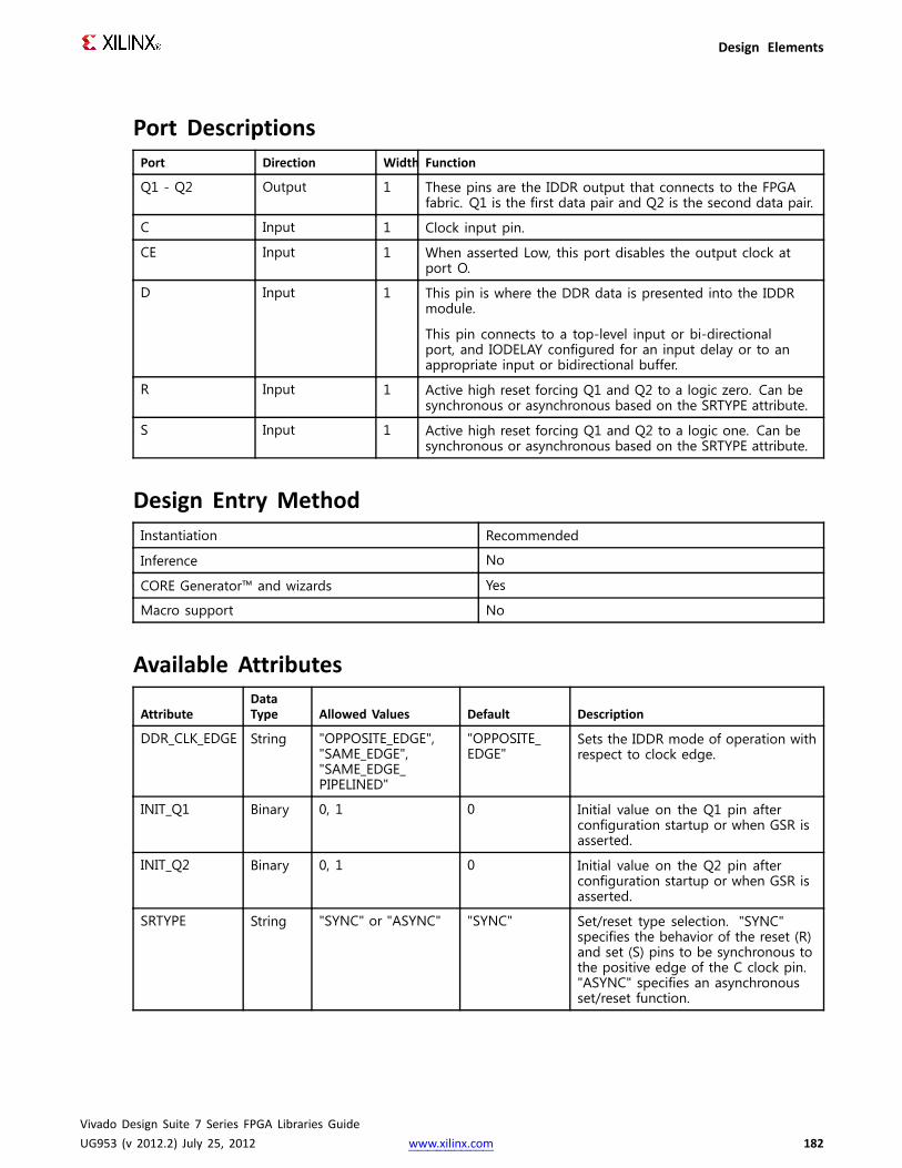
Design Elements
Port DescriptionsPort Direction Width Function
Q1 - Q2 Output 1 These pins are the IDDR output that connects to the FPGAfabric. Q1 is the first data pair and Q2 is the second data pair.
C Input 1 Clock input pin.
CE Input 1 When asserted Low, this port disables the output clock atport O.
D Input 1 This pin is where the DDR data is presented into the IDDRmodule.
This pin connects to a top-level input or bi-directionalport, and IODELAY configured for an input delay or to anappropriate input or bidirectional buffer.
R Input 1 Active high reset forcing Q1 and Q2 to a logic zero. Can besynchronous or asynchronous based on the SRTYPE attribute.
S Input 1 Active high reset forcing Q1 and Q2 to a logic one. Can besynchronous or asynchronous based on the SRTYPE attribute.
Design Entry MethodInstantiation Recommended
Inference No
CORE Generator™ and wizards Yes
Macro support No
Available Attributes
AttributeDataType Allowed Values Default Description
DDR_CLK_EDGE String "OPPOSITE_EDGE","SAME_EDGE","SAME_EDGE_PIPELINED"
"OPPOSITE_EDGE"
Sets the IDDR mode of operation withrespect to clock edge.
INIT_Q1 Binary 0, 1 0 Initial value on the Q1 pin afterconfiguration startup or when GSR isasserted.
INIT_Q2 Binary 0, 1 0 Initial value on the Q2 pin afterconfiguration startup or when GSR isasserted.
SRTYPE String "SYNC" or "ASYNC" "SYNC" Set/reset type selection. "SYNC"specifies the behavior of the reset (R)and set (S) pins to be synchronous tothe positive edge of the C clock pin."ASYNC" specifies an asynchronousset/reset function.
Vivado Design Suite 7 Series FPGA Libraries GuideUG953 (v 2012.2) July 25, 2012 www.xilinx.com 182

Design Elements
VHDL Instantiation TemplateUnless they already exist, copy the following two statements and paste them before the entitydeclaration.Library UNISIM;use UNISIM.vcomponents.all;
-- IDDR: Double Data Rate Input Register with Set, Reset-- and Clock Enable.-- 7 Series-- Xilinx HDL Libraries Guide, version 2012.2
IDDR_inst : IDDRgeneric map (
DDR_CLK_EDGE=> "OPPOSITE_EDGE", -- "OPPOSITE_EDGE", "SAME_EDGE"-- or "SAME_EDGE_PIPELINED"
INIT_Q1 => '0', -- Initial value of Q1: '0' or '1'INIT_Q2 => '0', -- Initial value of Q2: '0' or '1'SRTYPE => "SYNC") -- Set/Reset type: "SYNC" or "ASYNC"
port map (Q1 => Q1, -- 1-bit output for positive edge of clockQ2 => Q2, -- 1-bit output for negative edge of clockC => C, -- 1-bit clock inputCE => CE, -- 1-bit clock enable inputD => D, -- 1-bit DDR data inputR => R, -- 1-bit resetS => S -- 1-bit set);
-- End of IDDR_inst instantiation
Verilog Instantiation Template
// IDDR: Input Double Data Rate Input Register with Set, Reset// and Clock Enable.// 7 Series// Xilinx HDL Libraries Guide, version 2012.2
IDDR #(.DDR_CLK_EDGE("OPPOSITE_EDGE"), // "OPPOSITE_EDGE", "SAME_EDGE"
// or "SAME_EDGE_PIPELINED".INIT_Q1(1'b0), // Initial value of Q1: 1'b0 or 1'b1.INIT_Q2(1'b0), // Initial value of Q2: 1'b0 or 1'b1.SRTYPE("SYNC") // Set/Reset type: "SYNC" or "ASYNC"
) IDDR_inst (.Q1(Q1), // 1-bit output forr positive edge of clock.Q2(Q2), // 1-bit output forr negative edge of clock.C(C), // 1-bit clock input.CE(CE), // 1-bit clock enable input.D(D), // 1-bit DDR data input.R(R), // 1-bit reset.S(S) // 1-bit set
);
// End of IDDR_inst instantiation
For More InformationSee the 7 series FPGA User Documentation (User Guides and Data Sheets).
Vivado Design Suite 7 Series FPGA Libraries GuideUG953 (v 2012.2) July 25, 2012 www.xilinx.com 183

Design Elements
IDDR_2CLKPrimitive: Input Dual Data-Rate Register with Dual Clock Inputs
IntroductionThis design element is a dedicated input register designed to receive external dual data rate(DDR) signals into Xilinx® FPGAs. You should only use the IDDR_2CLK for very high speedinterfaces, since it requires more clocking resources, more power, and can imply certainplacement restrictions that are not necessary when using the IDDR component. The IDDRcomponent is also easier to use, uses fewer resources, and has fewer restrictions, though itcannot operate at the same high I/O speeds. The IDDR_2CLK is available with modes thatpresent the data to the FPGA fabric at the time and clock edge they are captured, or on thesame clock edge. This feature allows designers to avoid additional timing complexities andresource usage.
• OPPOSITE_EDGE mode: Data is presented in the classic DDR methodology. Given aDDR data and clock at pin D and C respectively, Q1 changes after every positive edge ofclock C, and Q2 changes after every positive edge of clock CB.
• SAME_EDGE mode: Data is still presented by positive edges of each clock. However,an extra register has been placed in front of the CB clocked data register. This extraregister is clocked with positive clock edge of clock signal C. As a result, DDR data isnow presented into the FPGA fabric at the positive edge of clock C. However, because ofthis feature, the data pair appears to be "separated." Q1 and Q2 no longer have pair1 and 2. Instead, the first pair presented is Pair 1 and DON'T CARE, followed by Pair2 and 3 at the next clock cycle.
• SAME_EDGE_PIPELINED mode: Presents data in a similar fashion as the SAME_EDGEmode. In order to avoid the "separated" effect of the SAME_EDGE mode, an extraregister has been placed in front of the C clocked data register. A data pair now appearsat the Q1 and Q2 pin at the same time during the positive edge of C. However, usingthis mode requires an additional cycle of latency for Q1 and Q2 signals to change.
IDDR also works with SelectIO™ features, such as the IODELAYE2.
Vivado Design Suite 7 Series FPGA Libraries GuideUG953 (v 2012.2) July 25, 2012 www.xilinx.com 184

Design Elements
Port DescriptionsPort Direction Width Function
Q1 : Q2 Output 1 These pins are the IDDR output that connects to theFPGA fabric. Q1 is the first data pair and Q2 is thesecond data pair.
C Input 1 Primary clock input pin used to capture the positiveedge data.
CB Input 1 Secondary clock input pin (typically 180 degrees outof phase with the primary clock) used to capture thenegative edge data.
CE Input 1 When asserted Low, this port disables the outputclock at port O.
D Input 1 This pin is where the DDR data is presented into theIDDR module.
This pin connects to a top-level input or bi-directionalport, and IODELAY configured for an input delay orto an appropriate input or bidirectional buffer.
R Input 1 Active high reset forcing Q1 and Q2 to a logic zero.Can be synchronous or asynchronous based on theSRTYPE attribute.
S Input 1 Active high reset forcing Q1 and Q2 to a logic one.Can be synchronous or asynchronous based on theSRTYPE attribute.
Design Entry MethodInstantiation Recommended
Inference No
CORE Generator™ and wizards No
Macro support No
• Connect the C pin to the appropriate clock source, representing the positive clock edgeand CB to the clock source representing the negative clock edge.
• Connect the D pin to the top-level input, or bidirectional port, an IODELAY, or aninstantiated input or bidirectional buffer.
• The Q1 and Q2 pins should be connected to the appropriate data sources.• CE should be tied high when not used, or connected to the appropriate clock enable
logic.• R and S pins should be tied low, if not used, or to the appropriate set or reset
generation logic.• Set all attributes to the component to represent the desired behavior.• Always instantiate this component in pairs with the same clocking, and to LOC those to
the appropriate P and N I/O pair in order not to sacrifice possible I/O resources.• Always instantiate this component in the top-level hierarchy of your design, along with
any other instantiated I/O components for the design. This helps facilitate hierarchicaldesign flows/practices.
Vivado Design Suite 7 Series FPGA Libraries GuideUG953 (v 2012.2) July 25, 2012 www.xilinx.com 185

Design Elements
• To minimize CLK skew, both CLK and CLKB should come from global routing (MMCM)and not from the local inversion. MMCM de-skews these clocks whereas the localinversion adds skew.
Available AttributesAttribute Data Type Allowed Values Default Description
DDR_CLK_EDGE String "OPPOSITE_EDGE","SAME_EDGE""SAME_EDGE_PIPELINED"
"OPPOSITE_EDGE"
DDR clock mode recovery modeselection. See Introduction formore explanation.
INIT_Q1 Binary 0, 1 0 Initial value on the Q1 pin afterconfiguration startup or whenGSR is asserted.
INIT_Q2 Binary 0, 1 0 Initial value on the Q2 pin afterconfiguration startup or whenGSR is asserted.
SRTYPE String "SYNC" or "ASYNC" "SYNC" Set/reset type selection. SYNC"specifies the behavior of thereset (R) and set (S) pins to besynchronous to the positive edgeof the C clock pin. "ASYNC"specifies an asynchronousset/reset function.
VHDL Instantiation TemplateUnless they already exist, copy the following two statements and paste them before the entitydeclaration.Library UNISIM;use UNISIM.vcomponents.all;
-- IDDR_2CLK: Dual-Clock, Input Double Data Rate Input Register with-- Set, Reset and Clock Enable.-- 7 Series-- Xilinx HDL Libraries Guide, version 2012.2
IDDR_2CLK_inst : IDDR_2CLKgeneric map (
DDR_CLK_EDGE=> "OPPOSITE_EDGE", -- "OPPOSITE_EDGE", "SAME_EDGE"-- or "SAME_EDGE_PIPELINED"
INIT_Q1 => '0', -- Initial value of Q1: '0' or '1'INIT_Q2 => '0', -- Initial value of Q2: '0' or '1'SRTYPE => "SYNC") -- Set/Reset type: "SYNC" or "ASYNC"
port map (Q1 => Q1, -- 1-bit output for positive edge of clockQ2 => Q2, -- 1-bit output for negative edge of clockC => C, -- 1-bit primary clock inputCB => CB, -- 1-bit secondary clock inputCE => CE, -- 1-bit clock enable inputD => D, -- 1-bit DDR data inputR => R, -- 1-bit resetS => S -- 1-bit set);
-- End of IDDR_2CLK_inst instantiation
Vivado Design Suite 7 Series FPGA Libraries GuideUG953 (v 2012.2) July 25, 2012 www.xilinx.com 186

Design Elements
Verilog Instantiation Template
// IDDR_2CLK: Dual-Clock, Input Double Data Rate Input Register with// Set, Reset and Clock Enable.// 7 Series// Xilinx HDL Libraries Guide, version 2012.2
IDDR_2CLK #(.DDR_CLK_EDGE("OPPOSITE_EDGE"), // "OPPOSITE_EDGE", "SAME_EDGE"
// or "SAME_EDGE_PIPELINED".INIT_Q1(1'b0), // Initial value of Q1: 1'b0 or 1'b1.INIT_Q2(1'b0), // Initial value of Q2: 1'b0 or 1'b1.SRTYPE("SYNC") // Set/Reset type: "SYNC" or "ASYNC"
) IDDR_2CLK_inst (.Q1(Q1), // 1-bit output forr positive edge of clock.Q2(Q2), // 1-bit output forr negative edge of clock.C(C), // 1-bit primary clock input.CB(CB), // 1-bit secondary clock input.CE(CE), // 1-bit clock enable input.D(D), // 1-bit DDR data input.R(R), // 1-bit reset.S(S) // 1-bit set
);
// End of IDDR_2CLK_inst instantiation
For More InformationSee the 7 series FPGA User Documentation (User Guides and Data Sheets).
Vivado Design Suite 7 Series FPGA Libraries GuideUG953 (v 2012.2) July 25, 2012 www.xilinx.com 187
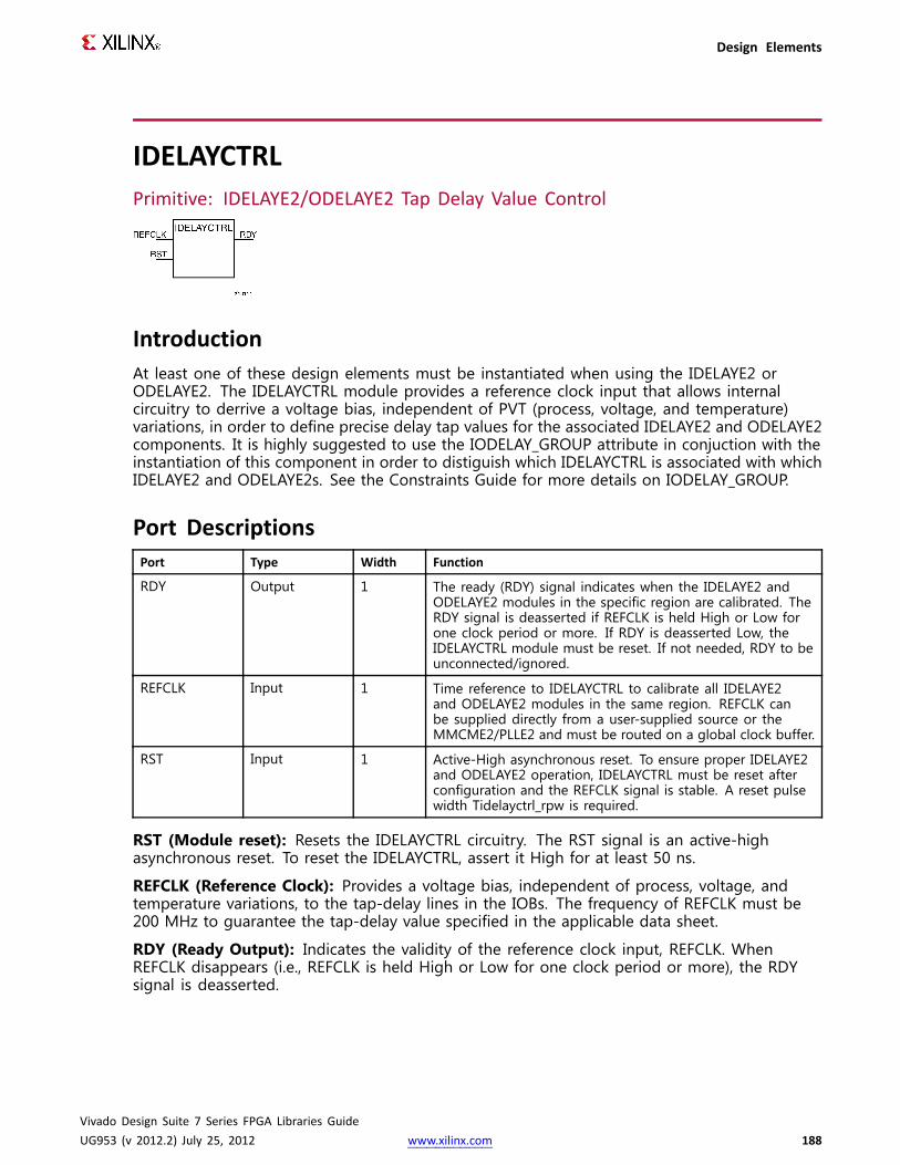
Design Elements
IDELAYCTRLPrimitive: IDELAYE2/ODELAYE2 Tap Delay Value Control
IntroductionAt least one of these design elements must be instantiated when using the IDELAYE2 orODELAYE2. The IDELAYCTRL module provides a reference clock input that allows internalcircuitry to derrive a voltage bias, independent of PVT (process, voltage, and temperature)variations, in order to define precise delay tap values for the associated IDELAYE2 and ODELAYE2components. It is highly suggested to use the IODELAY_GROUP attribute in conjuction with theinstantiation of this component in order to distiguish which IDELAYCTRL is associated with whichIDELAYE2 and ODELAYE2s. See the Constraints Guide for more details on IODELAY_GROUP.
Port DescriptionsPort Type Width Function
RDY Output 1 The ready (RDY) signal indicates when the IDELAYE2 andODELAYE2 modules in the specific region are calibrated. TheRDY signal is deasserted if REFCLK is held High or Low forone clock period or more. If RDY is deasserted Low, theIDELAYCTRL module must be reset. If not needed, RDY to beunconnected/ignored.
REFCLK Input 1 Time reference to IDELAYCTRL to calibrate all IDELAYE2and ODELAYE2 modules in the same region. REFCLK canbe supplied directly from a user-supplied source or theMMCME2/PLLE2 and must be routed on a global clock buffer.
RST Input 1 Active-High asynchronous reset. To ensure proper IDELAYE2and ODELAYE2 operation, IDELAYCTRL must be reset afterconfiguration and the REFCLK signal is stable. A reset pulsewidth Tidelayctrl_rpw is required.
RST (Module reset): Resets the IDELAYCTRL circuitry. The RST signal is an active-highasynchronous reset. To reset the IDELAYCTRL, assert it High for at least 50 ns.
REFCLK (Reference Clock): Provides a voltage bias, independent of process, voltage, andtemperature variations, to the tap-delay lines in the IOBs. The frequency of REFCLK must be200 MHz to guarantee the tap-delay value specified in the applicable data sheet.
RDY (Ready Output): Indicates the validity of the reference clock input, REFCLK. WhenREFCLK disappears (i.e., REFCLK is held High or Low for one clock period or more), the RDYsignal is deasserted.
Vivado Design Suite 7 Series FPGA Libraries GuideUG953 (v 2012.2) July 25, 2012 www.xilinx.com 188

Design Elements
Design Entry MethodInstantiation Yes
Inference No
CORE Generator™ and wizards Yes
Macro support No
VHDL Instantiation TemplateUnless they already exist, copy the following two statements and paste them before the entitydeclaration.Library UNISIM;use UNISIM.vcomponents.all;
-- IDELAYCTRL: IDELAYE2/ODELAYE2 Tap Delay Value Control-- 7 Series-- Xilinx HDL Libraries Guide, version 2012.2
IDELAYCTRL_inst : IDELAYCTRLport map (
RDY => RDY, -- 1-bit output: Ready outputREFCLK => REFCLK, -- 1-bit input: Reference clock inputRST => RST -- 1-bit input: Active high reset input
);
-- End of IDELAYCTRL_inst instantiation
Verilog Instantiation Template
// IDELAYCTRL: IDELAYE2/ODELAYE2 Tap Delay Value Control// 7 Series// Xilinx HDL Libraries Guide, version 2012.2
(* IODELAY_GROUP= <iodelay_group_name> *) // Specifies group name for associated IDELAYs/ODELAYs and IDELAYCTRL
IDELAYCTRL IDELAYCTRL_inst (.RDY(RDY), // 1-bit output: Ready output.REFCLK(REFCLK), // 1-bit input: Reference clock input.RST(RST) // 1-bit input: Active high reset input
);
// End of IDELAYCTRL_inst instantiation
For More InformationSee the 7 series FPGA User Documentation (User Guides and Data Sheets).
Vivado Design Suite 7 Series FPGA Libraries GuideUG953 (v 2012.2) July 25, 2012 www.xilinx.com 189

Design Elements
IDELAYE2Primitive: Input Fixed or Variable Delay Element
IntroductionEvery I/O block contains a programmable absolute delay element called IDELAYE2. TheIDELAYE2 can be connected to an input register/ISERDESE1 or driven directly into FPGA logic.The IDELAYE2 is a 31-tap, wraparound, delay element with a calibrated tap resolution. Refer tothe 7 series FPGA Data Sheet for delay values. The IDELAYE2 allows incoming signals to bedelayed on an individual basis. The tap delay resolution is varied by selecting an IDELAYCTRLreference clock from the range specified in the 7 series FPGA Data Sheet.
Port DescriptionsPort Type Width Function
C Input 1 All control inputs to IDELAYE2 primitive (RST, CE, and INC) aresynchronous to the clock input (C). A clock must be connectedto this port when IDELAYE2 is configured in "VARIABLE","VAR_LOAD" or "VAR_LOAD_PIPE" mode. C can be locallyinverted, and must be supplied by a global or regional clockbuffer. This clock should be connected to the same clockin the SelectIO logic resources (when using ISERDESE2 andOSERDESE2, C is connected to CLKDIV).
CE Input 1 Active high enable increment/decrement function
CINVCTRL Input 1 The CINVCTRL pin is used for dynamically switching thepolarity of C pin. This is for use in applications when glitchesare not an issue. When switching the polarity, do not use theIDELAYE2 control pins for two clock cycles.
CNTVALUEIN<4:0>
Input 5 Counter value from FPGA logic for dynamically loadable tapvalue input.
CNTVALUEOUT<4:0>
Output 5 The CNTVALUEOUT pins are used for reporting the dynamicallyswitching value of the delay element. CNTVALUEOUT is onlyavailable when IDELAYE2 is in "VAR_LOAD" or "VAR_LOAD_PIPE"mode.
Vivado Design Suite 7 Series FPGA Libraries GuideUG953 (v 2012.2) July 25, 2012 www.xilinx.com 190
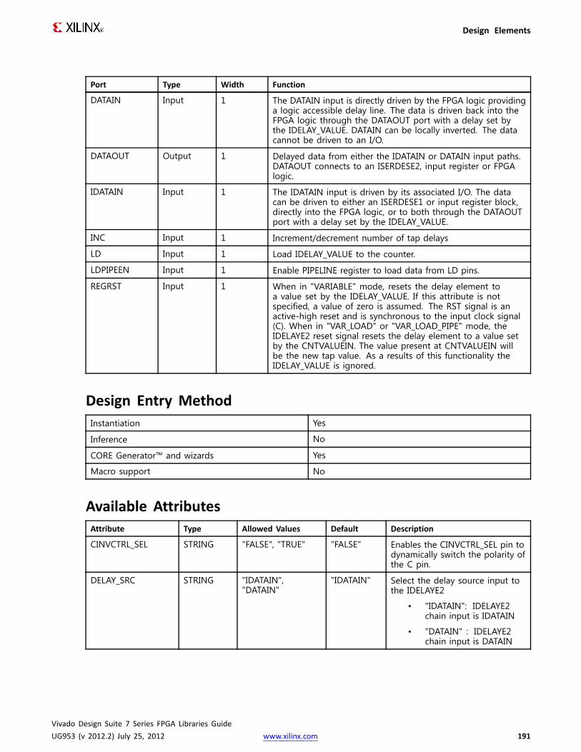
Design Elements
Port Type Width Function
DATAIN Input 1 The DATAIN input is directly driven by the FPGA logic providinga logic accessible delay line. The data is driven back into theFPGA logic through the DATAOUT port with a delay set bythe IDELAY_VALUE. DATAIN can be locally inverted. The datacannot be driven to an I/O.
DATAOUT Output 1 Delayed data from either the IDATAIN or DATAIN input paths.DATAOUT connects to an ISERDESE2, input register or FPGAlogic.
IDATAIN Input 1 The IDATAIN input is driven by its associated I/O. The datacan be driven to either an ISERDESE1 or input register block,directly into the FPGA logic, or to both through the DATAOUTport with a delay set by the IDELAY_VALUE.
INC Input 1 Increment/decrement number of tap delays
LD Input 1 Load IDELAY_VALUE to the counter.
LDPIPEEN Input 1 Enable PIPELINE register to load data from LD pins.
REGRST Input 1 When in "VARIABLE" mode, resets the delay element toa value set by the IDELAY_VALUE. If this attribute is notspecified, a value of zero is assumed. The RST signal is anactive-high reset and is synchronous to the input clock signal(C). When in "VAR_LOAD" or "VAR_LOAD_PIPE" mode, theIDELAYE2 reset signal resets the delay element to a value setby the CNTVALUEIN. The value present at CNTVALUEIN willbe the new tap value. As a results of this functionality theIDELAY_VALUE is ignored.
Design Entry MethodInstantiation Yes
Inference No
CORE Generator™ and wizards Yes
Macro support No
Available AttributesAttribute Type Allowed Values Default Description
CINVCTRL_SEL STRING "FALSE", "TRUE" "FALSE" Enables the CINVCTRL_SEL pin todynamically switch the polarity ofthe C pin.
DELAY_SRC STRING "IDATAIN","DATAIN"
"IDATAIN" Select the delay source input tothe IDELAYE2
• "IDATAIN": IDELAYE2chain input is IDATAIN
• "DATAIN" : IDELAYE2chain input is DATAIN
Vivado Design Suite 7 Series FPGA Libraries GuideUG953 (v 2012.2) July 25, 2012 www.xilinx.com 191

Design Elements
Attribute Type Allowed Values Default Description
HIGH_PERFORMANCE_MODE
STRING "FALSE", "TRUE" "FALSE" When TRUE, this attributereduces the output jitter. WhenFALSE, power consumption isreduced. The difference in powerconsumption is quantified in theXilinx Power Estimator tool.
IDELAY_TYPE STRING "FIXED","VARIABLE","VAR_LOAD","VAR_LOAD_PIPE"
"FIXED" Sets the type of tap delay line.
• "FIXED" - Sets a staticdelay value.
• "VARIABLE" -Dynamically adjust(incement/decrement)delay value.
• "VAR_LOAD" -Dynamically loads tapvalues.
• "VAR_LOAD_PIPE" -Pipelined dynamicallyloadable tap values.
IDELAY_VALUE DECIMAL 0, 1, 2, 3, 4, 5, 6, 7,8, 9, 10, 11, 12, 13,14, 15, 16, 17, 18,19, 20, 21, 22, 23,24, 25, 26, 27, 28,29, 30, 31
0 Specifies the fixed number ofdelay taps in fixed mode or theinitial starting number of taps in"VARIABLE" mode (input path).When IDELAY_TYPE is set to"VAR_LOAD" or "VAR_LOAD_PIPE"mode, this value is ignored.
PIPE_SEL STRING "FALSE", "TRUE" "FALSE" Select pipelined mode.
REFCLK_FREQUENCY
1 significantdigit FLOAT
190.0 to 210.0 and290.0 to 310.0
200.0 Sets the tap value (in MHz)used by the timing analyzerfor static timing analysis andfunctional/timing simulation. Thefrequency of REFCLK must bewithin the given datasheet rangeto guarantee the tap-delay valueand performance.
SIGNAL _PATTERN STRING "DATA", "CLOCK" "DATA" Causes the timing analyzer toaccount for the appropriateamount of delay-chain jitter inthe data or clock path.
VHDL Instantiation TemplateUnless they already exist, copy the following two statements and paste them before the entitydeclaration.Library UNISIM;use UNISIM.vcomponents.all;
-- IDELAYE2: Input Fixed or Variable Delay Element-- 7 Series-- Xilinx HDL Libraries Guide, version 2012.2
IDELAYE2_inst : IDELAYE2
Vivado Design Suite 7 Series FPGA Libraries GuideUG953 (v 2012.2) July 25, 2012 www.xilinx.com 192

Design Elements
generic map (CINVCTRL_SEL => "FALSE", -- Enable dynamic clock inversion (FALSE, TRUE)DELAY_SRC=> "IDATAIN", -- Delay input (IDATAIN, DATAIN)HIGH_PERFORMANCE_MODE=> "FALSE", -- Reduced jitter ("TRUE"), Reduced power ("FALSE")IDELAY_TYPE => "FIXED", -- FIXED, VARIABLE, VAR_LOAD, VAR_LOAD_PIPEIDELAY_VALUE => 0, -- Input delay tap setting (0-31)PIPE_SEL => "FALSE", -- Select pipelined mode, FALSE, TRUEREFCLK_FREQUENCY=> 200.0, -- IDELAYCTRL clock input frequency in MHz (190.0-210.0).SIGNAL_PATTERN=> "DATA" -- DATA, CLOCK input signal
)port map (
CNTVALUEOUT=> CNTVALUEOUT,-- 5-bit output: Counter value outputDATAOUT=> DATAOUT, -- 1-bit output: Delayed data outputC => C, -- 1-bit input: Clock inputCE => CE, -- 1-bit input: Active high enable increment/decrement inputCINVCTRL => CINVCTRL, -- 1-bit input: Dynamic clock inversion inputCNTVALUEIN => CNTVALUEIN, -- 5-bit input: Counter value inputDATAIN => DATAIN, -- 1-bit input: Internal delay data inputIDATAIN => IDATAIN, -- 1-bit input: Data input from the I/OINC => INC, -- 1-bit input: Increment / Decrement tap delay inputLD => LD, -- 1-bit input: Load IDELAY_VALUE inputLDPIPEEN => LDPIPEEN, -- 1-bit input: Enable PIPELINE register to load data inputREGRST=> REGRST -- 1-bit input: Active-high reset tap-delay input
);
-- End of IDELAYE2_inst instantiation
Verilog Instantiation Template
// IDELAYE2: Input Fixed or Variable Delay Element// 7 Series// Xilinx HDL Libraries Guide, version 2012.2
(* IODELAY_GROUP= <iodelay_group_name> *) // Specifies group name for associated IDELAYs/ODELAYs and IDELAYCTRL
IDELAYE2 #(.CINVCTRL_SEL("FALSE"), // Enable dynamic clock inversion (FALSE, TRUE).DELAY_SRC("IDATAIN"), // Delay input (IDATAIN, DATAIN).HIGH_PERFORMANCE_MODE("FALSE"), // Reduced jitter ("TRUE"), Reduced power ("FALSE").IDELAY_TYPE("FIXED"), // FIXED, VARIABLE, VAR_LOAD, VAR_LOAD_PIPE.IDELAY_VALUE(0), // Input delay tap setting (0-31).PIPE_SEL("FALSE"), // Select pipelined mode, FALSE, TRUE.REFCLK_FREQUENCY(200.0), // IDELAYCTRL clock input frequency in MHz (190.0-210.0)..SIGNAL_PATTERN("DATA") // DATA, CLOCK input signal
)IDELAYE2_inst (
.CNTVALUEOUT(CNTVALUEOUT),// 5-bit output: Counter value output
.DATAOUT(DATAOUT), // 1-bit output: Delayed data output
.C(C), // 1-bit input: Clock input
.CE(CE), // 1-bit input: Active high enable increment/decrement input
.CINVCTRL(CINVCTRL), // 1-bit input: Dynamic clock inversion input
.CNTVALUEIN(CNTVALUEIN), // 5-bit input: Counter value input
.DATAIN(DATAIN), // 1-bit input: Internal delay data input
.IDATAIN(IDATAIN), // 1-bit input: Data input from the I/O
.INC(INC), // 1-bit input: Increment / Decrement tap delay input
.LD(LD), // 1-bit input: Load IDELAY_VALUE input
.LDPIPEEN(LDPIPEEN), // 1-bit input: Enable PIPELINE register to load data input
.REGRST(REGRST) // 1-bit input: Active-high reset tap-delay input);
// End of IDELAYE2_inst instantiation
For More InformationSee the 7 series FPGA User Documentation (User Guides and Data Sheets).
Vivado Design Suite 7 Series FPGA Libraries GuideUG953 (v 2012.2) July 25, 2012 www.xilinx.com 193

Design Elements
IN_FIFOPrimitive: Input First-In, First-Out (FIFO)
IntroductionThe Input FIFO is a new resource located next to the I/O. This dedicated hardware is designedto help transition the data from the input port, input register, IDDR or ISERDES to the fabric. Ithas two basic modes the first is a 4x4 mode where the data coming into the FIFO goes out atthe same rate. The second mode is a 4x8 mode where the data coming out is de-serializedby a factor of 2. In other words in 4x8 mode 4 bits go to the IN_FIFO and 8 bits come out.Features of this component include:
• Array dimensions: 80 wide, 8 deep (4x8 mode); 40 wide, 8 deep (4x4 mode)
• Empty and Full flags
• Programmable Almost Empty and Almost Full flags
Vivado Design Suite 7 Series FPGA Libraries GuideUG953 (v 2012.2) July 25, 2012 www.xilinx.com 194

Design Elements
Port DescriptionsPort Type Width Function
ALMOSTEMPTY Output 1 Active high output flag indicating the FIFO is almost empty.The threshold of the almost empty flag is set by theALMOST_EMPTY_VALUE attribute.
ALMOSTFULL Output 1 Active high output flag indicating the FIFO is almost full.The threshold of the almost empty flag is set by theALMOST_FULL_VALUE attribute.
D0<3:0> Input 4 Channel 0 input bus.
D1<3:0> Input 4 Channel 1 input bus.
D2<3:0> Input 4 Channel 2 input bus.
D3<3:0> Input 4 Channel 3 input bus.
D4<3:0> Input 4 Channel 4 input bus.
D5<7:0> Input 8 Channel 5 input bus.
D6<7:0> Input 8 Channel 6 input bus.
D7<3:0> Input 4 Channel 7 input bus.
D8<3:0> Input 4 Channel 8 input bus.
D9<3:0> Input 4 Channel 9 input bus.
EMPTY Output 1 Active high output flag indicating the FIFO is empty.
FULL Output 1 Active high output flag indicating the FIFO is full.
Q0<7:0> Output 8 Channel 0 input bus.
Q1<7:0> Output 8 Channel 1 output bus.
Q2<7:0> Output 8 Channel 2 output bus.
Q3<7:0> Output 8 Channel 3 output bus.
Q4<7:0> Output 8 Channel 4 output bus.
Q5<7:0> Output 8 Channel 5 output bus.
Q6<7:0> Output 8 Channel 6 output bus.
Q7<7:0> Output 8 Channel 7 output bus.
Q8<7:0> Output 8 Channel 8 output bus.
Q9<7:0> Output 8 Channel 9 output bus.
RDCLK Input 1 Read clock.
RDEN Input 1 Active high read enable.
RESET Input 1 Active low, asynchrnous reset.
WRCLK Input 1 Write clock.
WREN Input 1 Active high write enable.
Vivado Design Suite 7 Series FPGA Libraries GuideUG953 (v 2012.2) July 25, 2012 www.xilinx.com 195

Design Elements
Design Entry MethodInstantiation Yes
Inference No
CORE Generator™ and wizards No
Macro support No
Available AttributesAttribute Type Allowed Values Default Description
ALMOST_EMPTY_VALUE
DECIMAL1, 2 1 Specifies the number of entriesleft before asserting theALMOSTEMPTY output signal.
ALMOST_FULL_VALUE
DECIMAL1, 2 1 Specifies the number of entriesleft before asserting theALMOSTFULL output signal.
ARRAY_MODE STRING "ARRAY_MODE_4_X_8","ARRAY_MODE_4_X_4"
"ARRAY_MODE_4_X_8"Specifies deserializer mode:
• "ARRAY_MODE_8_X_8"- Eight bits in, eightbits out
• "ARRAY_MODE_4_X_8"- Four bits in, eightbits out
SYNCHRONOUS_MODE
STRING "FALSE" "FALSE" Specify whether the RDCLKand WRCLK are synchrnous toeach other.
VHDL Instantiation TemplateUnless they already exist, copy the following two statements and paste them before the entitydeclaration.Library UNISIM;use UNISIM.vcomponents.all;
-- IN_FIFO: Input First-In, First-Out (FIFO)-- 7 Series-- Xilinx HDL Libraries Guide, version 2012.2
IN_FIFO_inst : IN_FIFOgeneric map (
ALMOST_EMPTY_VALUE=> 1, -- Almost empty offset (1-2)ALMOST_FULL_VALUE=> 1, -- Almost full offset (1-2)ARRAY_MODE=> "ARRAY_MODE_4_X_8", -- ARRAY_MODE_4_X_8,ARRAY_MODE_4_X_4SYNCHRONOUS_MODE=> "FALSE" -- Clock synchronous (FALSE)
)port map (
-- FIFO Status Flags: 1-bit (each) output: Flags and other FIFO status outputsALMOSTEMPTY=> ALMOSTEMPTY,-- 1-bit output: Almost emptyALMOSTFULL=> ALMOSTFULL, -- 1-bit output: Almost fullEMPTY=> EMPTY, -- 1-bit output: EmptyFULL => FULL, -- 1-bit output: Full-- Q0-Q9: 8-bit (each) output: FIFO OutputsQ0 => Q0, -- 8-bit output: Channel 0Q1 => Q1, -- 8-bit output: Channel 1
Vivado Design Suite 7 Series FPGA Libraries GuideUG953 (v 2012.2) July 25, 2012 www.xilinx.com 196
Design Elements
Q2 => Q2, -- 8-bit output: Channel 2Q3 => Q3, -- 8-bit output: Channel 3Q4 => Q4, -- 8-bit output: Channel 4Q5 => Q5, -- 8-bit output: Channel 5Q6 => Q6, -- 8-bit output: Channel 6Q7 => Q7, -- 8-bit output: Channel 7Q8 => Q8, -- 8-bit output: Channel 8Q9 => Q9, -- 8-bit output: Channel 9-- D0-D9: 4-bit (each) input: FIFO inputsD0 => D0, -- 4-bit input: Channel 0D1 => D1, -- 4-bit input: Channel 1D2 => D2, -- 4-bit input: Channel 2D3 => D3, -- 4-bit input: Channel 3D4 => D4, -- 4-bit input: Channel 4D5 => D5, -- 8-bit input: Channel 5D6 => D6, -- 8-bit input: Channel 6D7 => D7, -- 4-bit input: Channel 7D8 => D8, -- 4-bit input: Channel 8D9 => D9, -- 4-bit input: Channel 9-- FIFO Control Signals: 1-bit (each) input: Clocks, Resets and EnablesRDCLK => RDCLK, -- 1-bit input: Read clockRDEN=> RDEN, -- 1-bit input: Read enableRESET => RESET, -- 1-bit input: ResetWRCLK=> WRCLK, -- 1-bit input: Write clockWREN=> WREN -- 1-bit input: Write enable
);
-- End of IN_FIFO_inst instantiation
Vivado Design Suite 7 Series FPGA Libraries GuideUG953 (v 2012.2) July 25, 2012 www.xilinx.com 197

Design Elements
Verilog Instantiation Template
// IN_FIFO: Input First-In, First-Out (FIFO)// 7 Series// Xilinx HDL Libraries Guide, version 2012.2
IN_FIFO #(.ALMOST_EMPTY_VALUE(1), // Almost empty offset (1-2).ALMOST_FULL_VALUE(1), // Almost full offset (1-2).ARRAY_MODE("ARRAY_MODE_4_X_8"), // ARRAY_MODE_4_X_8,ARRAY_MODE_4_X_4.SYNCHRONOUS_MODE("FALSE") // Clock synchronous (FALSE)
)IN_FIFO_inst (
// FIFO Status Flags: 1-bit (each) output: Flags and other FIFO status outputs.ALMOSTEMPTY(ALMOSTEMPTY),// 1-bit output: Almost empty.ALMOSTFULL(ALMOSTFULL), // 1-bit output: Almost full.EMPTY(EMPTY), // 1-bit output: Empty.FULL(FULL), // 1-bit output: Full// Q0-Q9: 8-bit (each) output: FIFO Outputs.Q0(Q0), // 8-bit output: Channel 0.Q1(Q1), // 8-bit output: Channel 1.Q2(Q2), // 8-bit output: Channel 2.Q3(Q3), // 8-bit output: Channel 3.Q4(Q4), // 8-bit output: Channel 4.Q5(Q5), // 8-bit output: Channel 5.Q6(Q6), // 8-bit output: Channel 6.Q7(Q7), // 8-bit output: Channel 7.Q8(Q8), // 8-bit output: Channel 8.Q9(Q9), // 8-bit output: Channel 9// D0-D9: 4-bit (each) input: FIFO inputs.D0(D0), // 4-bit input: Channel 0.D1(D1), // 4-bit input: Channel 1.D2(D2), // 4-bit input: Channel 2.D3(D3), // 4-bit input: Channel 3.D4(D4), // 4-bit input: Channel 4.D5(D5), // 8-bit input: Channel 5.D6(D6), // 8-bit input: Channel 6.D7(D7), // 4-bit input: Channel 7.D8(D8), // 4-bit input: Channel 8.D9(D9), // 4-bit input: Channel 9// FIFO Control Signals: 1-bit (each) input: Clocks, Resets and Enables.RDCLK(RDCLK), // 1-bit input: Read clock.RDEN(RDEN), // 1-bit input: Read enable.RESET(RESET), // 1-bit input: Reset.WRCLK(WRCLK), // 1-bit input: Write clock.WREN(WREN) // 1-bit input: Write enable
);
// End of IN_FIFO_inst instantiation
For More InformationSee the 7 series FPGA User Documentation (User Guides and Data Sheets).
Vivado Design Suite 7 Series FPGA Libraries GuideUG953 (v 2012.2) July 25, 2012 www.xilinx.com 198

Design Elements
IOBUFPrimitive: Bi-Directional Buffer
IntroductionThe design element is a bidirectional single-ended I/O Buffer used to connect internal logic toan external bidirectional pin.
Logic TableInputs Bidirectional Outputs
T I IO O
1 X Z IO
0 1 1 1
0 0 0 0
Port DescriptionsPort Direction Width Function
O Output 1 Buffer output
IO In/out 1 Buffer In/out
I Input 1 Buffer input
T Input 1 3-State enable input
Design Entry MethodInstantiation Yes
Inference Recommended
CORE Generator™ and wizards No
Macro support No
Vivado Design Suite 7 Series FPGA Libraries GuideUG953 (v 2012.2) July 25, 2012 www.xilinx.com 199

Design Elements
Available Attributes
AttributeDataType Allowed Values Default Description
DRIVE Integer 2, 4, 6, 8, 12, 16, 24 12 Selects output drive strength (mA)for the SelectIO™ buffers that usethe LVTTL, LVCMOS12, LVCMOS15,LVCMOS18, LVCMOS25, orLVCMOS33 interface I/O standard.
IOSTANDARD String See Data Sheet "DEFAULT" Assigns an I/O standard to theelement.
SLEW String "SLOW", "FAST" "SLOW" Sets the output rise and fall time.
VHDL Instantiation TemplateUnless they already exist, copy the following two statements and paste them before the entitydeclaration.Library UNISIM;use UNISIM.vcomponents.all;
-- IOBUF: Single-ended Bi-directional Buffer-- 7 Series-- Xilinx HDL Libraries Guide, version 2012.2
IOBUF_inst : IOBUFgeneric map (
DRIVE => 12,IOSTANDARD=> "DEFAULT",SLEW=> "SLOW")
port map (O => O, -- Buffer outputIO => IO, -- Buffer inout port (connect directly to top-level port)I => I, -- Buffer inputT => T -- 3-state enable input, high=input, low=output
);
-- End of IOBUF_inst instantiation
Verilog Instantiation Template
// IOBUF: Single-ended Bi-directional Buffer// All devices// Xilinx HDL Libraries Guide, version 2012.2
IOBUF #(.DRIVE(12), // Specify the output drive strength.IBUF_LOW_PWR("TRUE"), // Low Power - "TRUE", High Perforrmance = "FALSE".IOSTANDARD("DEFAULT"), // Specify the I/O standard.SLEW("SLOW") // Specify the output slew rate
) IOBUF_inst (.O(O), // Buffer output.IO(IO), // Buffer inout port (connect directly to top-level port).I(I), // Buffer input.T(T) // 3-state enable input, high=input, low=output
);
// End of IOBUF_inst instantiation
Vivado Design Suite 7 Series FPGA Libraries GuideUG953 (v 2012.2) July 25, 2012 www.xilinx.com 200

Design Elements
For More Information• See the 7 series FPGA SelectIO Resources User Guide (UG471).
• See the 7 series FPGA User Documentation (User Guides and Data Sheets).
Vivado Design Suite 7 Series FPGA Libraries GuideUG953 (v 2012.2) July 25, 2012 www.xilinx.com 201
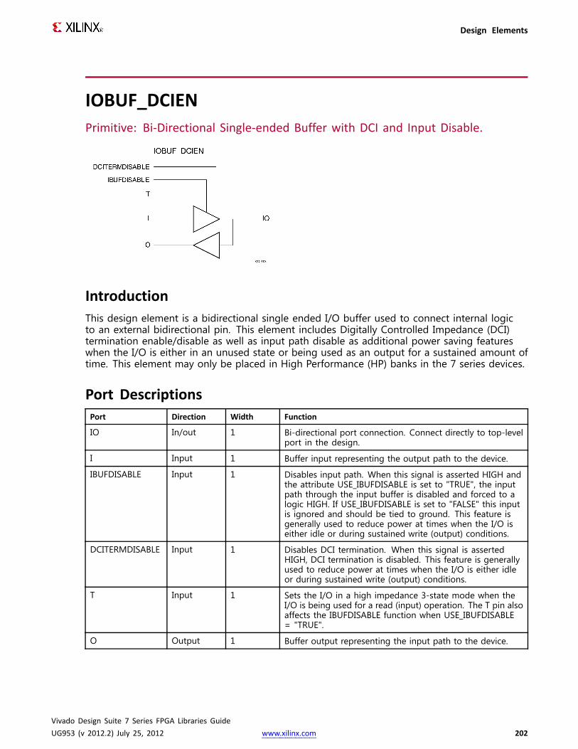
Design Elements
IOBUF_DCIENPrimitive: Bi-Directional Single-ended Buffer with DCI and Input Disable.
IntroductionThis design element is a bidirectional single ended I/O buffer used to connect internal logicto an external bidirectional pin. This element includes Digitally Controlled Impedance (DCI)termination enable/disable as well as input path disable as additional power saving featureswhen the I/O is either in an unused state or being used as an output for a sustained amount oftime. This element may only be placed in High Performance (HP) banks in the 7 series devices.
Port DescriptionsPort Direction Width Function
IO In/out 1 Bi-directional port connection. Connect directly to top-levelport in the design.
I Input 1 Buffer input representing the output path to the device.
IBUFDISABLE Input 1 Disables input path. When this signal is asserted HIGH andthe attribute USE_IBUFDISABLE is set to "TRUE", the inputpath through the input buffer is disabled and forced to alogic HIGH. If USE_IBUFDISABLE is set to "FALSE" this inputis ignored and should be tied to ground. This feature isgenerally used to reduce power at times when the I/O iseither idle or during sustained write (output) conditions.
DCITERMDISABLE Input 1 Disables DCI termination. When this signal is assertedHIGH, DCI termination is disabled. This feature is generallyused to reduce power at times when the I/O is either idleor during sustained write (output) conditions.
T Input 1 Sets the I/O in a high impedance 3-state mode when theI/O is being used for a read (input) operation. The T pin alsoaffects the IBUFDISABLE function when USE_IBUFDISABLE= "TRUE".
O Output 1 Buffer output representing the input path to the device.
Vivado Design Suite 7 Series FPGA Libraries GuideUG953 (v 2012.2) July 25, 2012 www.xilinx.com 202

Design Elements
Design Entry MethodInstantiation Yes
Inference No
CORE Generator™ and wizards Yes
Macro support No
Available Attributes
AttributeDataType Allowed Values Default Description
DRIVE Integer 2, 4, 6, 8, 12, 16, 24 12 Selects output drive strength (mA)for the SelectIO™ buffers.
IBUF_LOW_PWR
String "TRUE", "FALSE" "TRUE" Allows a trade off of lowerpower consumption vs. highestperformance.
IOSTANDARD String See Data Sheet "DEFAULT" Assigns an I/O standard to theelement.
SLEW String "SLOW", "FAST", "SLOW" Sets the output rise and falltime. See the Data Sheet forrecommendations of the bestsetting for this attribute.
USE_IBUFDISABLE
String "TRUE", "FALSE" "TRUE" Enables or disables the feature ofIBUFDISABLE. Set to FALSE when itis not desirable to have the T pindisable input path to allow a readduring write operation. When setto TRUE deasserting T (IO used asoutput) or asserting IBUFDISABLEwill disable the input path throughthe buffer and forces to a logichigh.
VHDL Instantiation TemplateUnless they already exist, copy the following two statements and paste them before the entitydeclaration.Library UNISIM;use UNISIM.vcomponents.all;
-- IOBUF_DCIEN: Single-ended Bi-directional Buffer with Digital Controlled Impedance (DCI)-- and Input path enable/disable-- May only be placed in High Performance (HP) Banks-- 7 Series-- Xilinx HDL Libraries Guide, version 2012.2
IOBUF_DCIEN_inst : IOBUF_DCIENgeneric map (
DRIVE => 12,IOSTANDARD=> "DEFAULT",IBUF_LOW_PWR=> "TRUE",SLEW=> "SLOW")
port map (O => O, -- Buffer output
Vivado Design Suite 7 Series FPGA Libraries GuideUG953 (v 2012.2) July 25, 2012 www.xilinx.com 203
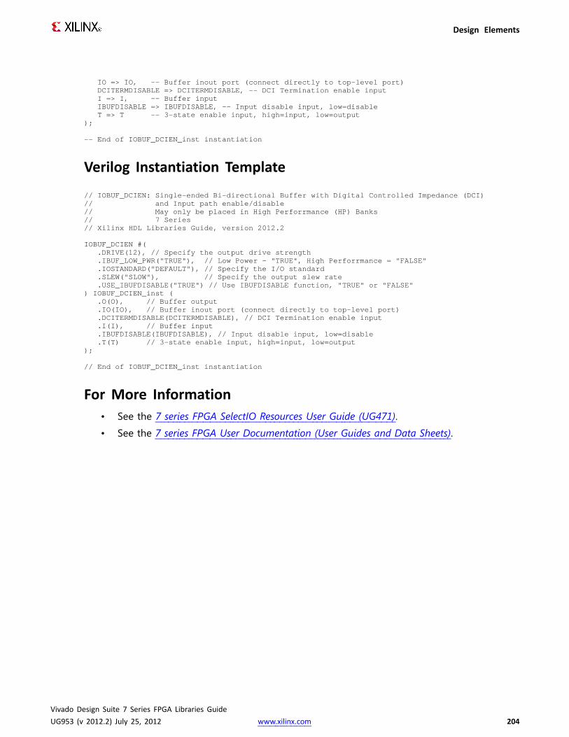
Design Elements
IO => IO, -- Buffer inout port (connect directly to top-level port)DCITERMDISABLE => DCITERMDISABLE, -- DCI Termination enable inputI => I, -- Buffer inputIBUFDISABLE => IBUFDISABLE, -- Input disable input, low=disableT => T -- 3-state enable input, high=input, low=output
);
-- End of IOBUF_DCIEN_inst instantiation
Verilog Instantiation Template
// IOBUF_DCIEN: Single-ended Bi-directional Buffer with Digital Controlled Impedance (DCI)// and Input path enable/disable// May only be placed in High Perforrmance (HP) Banks// 7 Series// Xilinx HDL Libraries Guide, version 2012.2
IOBUF_DCIEN #(.DRIVE(12), // Specify the output drive strength.IBUF_LOW_PWR("TRUE"), // Low Power - "TRUE", High Perforrmance = "FALSE".IOSTANDARD("DEFAULT"), // Specify the I/O standard.SLEW("SLOW"), // Specify the output slew rate.USE_IBUFDISABLE("TRUE") // Use IBUFDISABLE function, "TRUE" or "FALSE"
) IOBUF_DCIEN_inst (.O(O), // Buffer output.IO(IO), // Buffer inout port (connect directly to top-level port).DCITERMDISABLE(DCITERMDISABLE), // DCI Termination enable input.I(I), // Buffer input.IBUFDISABLE(IBUFDISABLE), // Input disable input, low=disable.T(T) // 3-state enable input, high=input, low=output
);
// End of IOBUF_DCIEN_inst instantiation
For More Information• See the 7 series FPGA SelectIO Resources User Guide (UG471).
• See the 7 series FPGA User Documentation (User Guides and Data Sheets).
Vivado Design Suite 7 Series FPGA Libraries GuideUG953 (v 2012.2) July 25, 2012 www.xilinx.com 204
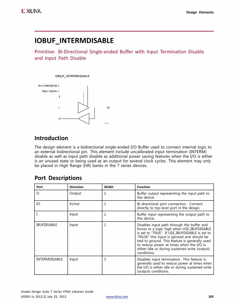
Design Elements
IOBUF_INTERMDISABLEPrimitive: Bi-Directional Single-ended Buffer with Input Termination Disableand Input Path Disable
IntroductionThe design element is a bidirectional single-ended I/O Buffer used to connect internal logic toan external bidirectional pin. This element include uncalibrated input termination (INTERM)disable as well as input path disable as additional power saving features when the I/O is eitheris an unused state or being used as an output for several clock cycles. This element may onlybe placed in High Range (HR) banks in the 7 series devices.
Port DescriptionsPort Direction Width Function
O Output 1 Buffer output representing the input path tothe device.
IO In/out 1 Bi-directional port connection. Connectdirectly to top-level port in the design.
I Input 1 Buffer input representing the output path tothe device.
IBUFDISABLE Input 1 Disables input path through the buffer andforces to a logic high when USE_IBUFDISABLEis set to "TRUE". If USE_IBUFDISABLE is set to"FALSE" this input is ignored and should betied to ground. This feature is generally usedto reduce power at times when the I/O iseither idle or during sustained write (output)conditions.
INTERMDISABLE Input 1 Disables input termination. This feature isgenerally used to reduce power at times whenthe I/O is either idle or during sustained write(output) conditions.
Vivado Design Suite 7 Series FPGA Libraries GuideUG953 (v 2012.2) July 25, 2012 www.xilinx.com 205
Design Elements
Port Direction Width Function
T Input 1 Sets the I/O in a high impedance 3-statemode when the I/O is being used for a read(input) operation. The T pin also affects theIBUFDISABLE function when USE_IBUFDISABLE= "TRUE". The T pin also disables INTERMwhen in a write (output) mode.
Design Entry MethodInstantiation Yes
Inference No
CORE Generator™ and wizards Yes
Macro support No
Available Attributes
AttributeDataType Allowed Values Default Description
DRIVE Integer 2, 4, 6, 8, 12, 16, 24 12 Selects output drive strength (mA)for the SelectIO™ buffers.
IBUF_LOW_PWR
String "TRUE", "FALSE" "TRUE" Allows a trade off of lowerpower consumption vs. highestperformance.
IOSTANDARD String See Data Sheet "DEFAULT" Assigns an I/O standard to theelement.
SLEW String "SLOW", "FAST" "SLOW" Sets the output rise and falltime. See the Data Sheet forrecommendations of the bestsetting for this attribute.
USE_IBUFDISABLE
String "TRUE", "FALSE" "TRUE" Enables or disables the feature ofIBUFDISABLE. Generally used whenit is not desirable to have the T pindisable input path to allow a readduring write operation.
VHDL Instantiation TemplateUnless they already exist, copy the following two statements and paste them before the entitydeclaration.Library UNISIM;use UNISIM.vcomponents.all;
-- IOBUF_INTERMDISABLE: Single-ended Bi-directional Buffer with Input Termination-- and Input path enable/disable-- May only be placed in High Range (HR) Banks-- 7 Series-- Xilinx HDL Libraries Guide, version 2012.2
IOBUF_INTERMDISABLE_inst : IOBUF_INTERMDISABLE
Vivado Design Suite 7 Series FPGA Libraries GuideUG953 (v 2012.2) July 25, 2012 www.xilinx.com 206

Design Elements
generic map (DRIVE => 12,IOSTANDARD=> "DEFAULT", -- Specify the I/O standardIBUF_LOW_PWR=> "TRUE", -- Low Power - "TRUE", High Performance = "FALSE"USE_IBUFDISABLE => "TRUE", -- Use IBUFDISABLE function "TRUE" or "FALSE"SLEW=> "SLOW")
port map (O => O, -- Buffer outputIO => IO, -- Buffer inout port (connect directly to top-level port)DCITERMDISABLE => DCITERMDISABLE, -- DCI Termination enable inputI => I, -- Buffer inputIBUFDISABLE => IBUFDISABLE, -- Input disable input, low=disableINTERMDISABLE => INTERMDISABLE, -- Input termination disable inputT => T -- 3-state enable input, high=input, low=output
);
-- End of IOBUF_INTERMDISABLE_inst instantiation
Verilog Instantiation Template
// IOBUF_INTERMDISABLE: Single-ended Bi-directional Buffer with Input Termination// and Input path enable/disable// May only be placed in High Range (HR) Banks// 7 Series// Xilinx HDL Libraries Guide, version 2012.2
IOBUF_INTERMDISABLE #(.DRIVE(12), // Specify the output drive strength.IBUF_LOW_PWR("TRUE"), // Low Power - "TRUE", High Perforrmance = "FALSE".IOSTANDARD("DEFAULT"), // Specify the I/O standard.SLEW("SLOW"), // Specify the output slew rate.USE_IBUFDISABLE("TRUE") // Use IBUFDISABLE function, "TRUE" or "FALSE"
) IOBUF_INTERMDISABLE_inst (.O(O), // Buffer output.IO(IO), // Buffer inout port (connect directly to top-level port).I(I), // Buffer input.IBUFDISABLE(IBUFDISABLE), // Input disable input, low=disable.INTERMDISABLE(INTERMDISABLE), // Input termination disable input.T(T) // 3-state enable input, high=input, low=output
);
// End of IOBUF_INTERMDISABLE_inst instantiation
For More Information• See the 7 series FPGA SelectIO Resources User Guide (UG471).
• See the 7 series FPGA User Documentation (User Guides and Data Sheets).
Vivado Design Suite 7 Series FPGA Libraries GuideUG953 (v 2012.2) July 25, 2012 www.xilinx.com 207
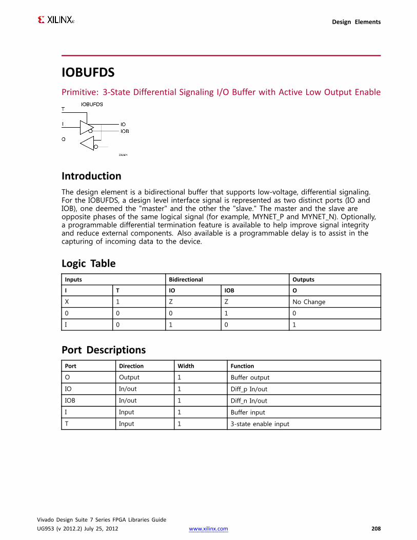
Design Elements
IOBUFDSPrimitive: 3-State Differential Signaling I/O Buffer with Active Low Output Enable
IntroductionThe design element is a bidirectional buffer that supports low-voltage, differential signaling.For the IOBUFDS, a design level interface signal is represented as two distinct ports (IO andIOB), one deemed the "master" and the other the "slave." The master and the slave areopposite phases of the same logical signal (for example, MYNET_P and MYNET_N). Optionally,a programmable differential termination feature is available to help improve signal integrityand reduce external components. Also available is a programmable delay is to assist in thecapturing of incoming data to the device.
Logic TableInputs Bidirectional Outputs
I T IO IOB O
X 1 Z Z No Change
0 0 0 1 0
I 0 1 0 1
Port DescriptionsPort Direction Width Function
O Output 1 Buffer output
IO In/out 1 Diff_p In/out
IOB In/out 1 Diff_n In/out
I Input 1 Buffer input
T Input 1 3-state enable input
Vivado Design Suite 7 Series FPGA Libraries GuideUG953 (v 2012.2) July 25, 2012 www.xilinx.com 208
Design Elements
Design Entry MethodInstantiation Recommended
Inference No
CORE Generator™ and wizards No
Macro support No
Available Attributes
AttributeDataType Allowed Values Default Description
DIFF_TERM Boolean TRUE, FALSE FALSE The differential terminationattribute is designed for the 7Series FPGA supported differentialinput I/O standards. It is usedto turn the built-in differentialtermination on (TRUE) or off(FALSE).
IBUF_LOW_PWR Boolean TRUE, FALSE TRUE When set to TRUE, allows forreduced power when usingdifferential or referenced (requiringVREF) input standards like LVDSor HSTL. A setting of FALSEdemands more power but delivershigher performance characteristics.Consult the 7 Series FPGA SelectIOResources User Guide for details.
IOSTANDARD String See Data Sheet "DEFAULT" Assigns an I/O standard to theelement.
SLEW String "SLOW" or"FAST"
"SLOW" Specifies the slew rate of theoutput driver. Consult the productData Sheet for recommendationsof the best setting for this attribute.
VHDL Instantiation TemplateUnless they already exist, copy the following two statements and paste them before the entitydeclaration.Library UNISIM;use UNISIM.vcomponents.all;
-- IOBUFDS: Differential Bi-directional Buffer-- 7 Series-- Xilinx HDL Libraries Guide, version 2012.2
IOBUFDS_inst : IOBUFDSgeneric map (
DIFF_TERM => FALSE, -- Differential Termination (TRUE/FALSE)IBUF_LOW_PWR=> TRUE, -- Low Power = TRUE, High Performance = FALSEIOSTANDARD=> "BLVDS_25", -- Specify the I/O standardSLEW=> "SLOW") -- Specify the output slew rate
port map (O => O, -- Buffer outputIO => IO, -- Diff_p inout (connect directly to top-level port)
Vivado Design Suite 7 Series FPGA Libraries GuideUG953 (v 2012.2) July 25, 2012 www.xilinx.com 209

Design Elements
IOB => IOB, -- Diff_n inout (connect directly to top-level port)I => I, -- Buffer inputT => T -- 3-state enable input, high=input, low=output
);
-- End of IOBUFDS_inst instantiation
Verilog Instantiation Template
// IOBUFDS: Differential Bi-directional Buffer// 7 Series// Xilinx HDL Libraries Guide, version 2012.2
IOBUFDS #(.DIFF_TERM("FALSE"), // Differential Termination ("TRUE"/"FALSE").IBUF_LOW_PWR("TRUE"), // Low Power - "TRUE", High Perforrmance = "FALSE".IOSTANDARD("BLVDS_25"), // Specify the I/O standard.SLEW("SLOW") // Specify the output slew rate
) IOBUFDS_inst (.O(O), // Buffer output.IO(IO), // Diff_p inout (connect directly to top-level port).IOB(IOB), // Diff_n inout (connect directly to top-level port).I(I), // Buffer input.T(T) // 3-state enable input, high=input, low=output
);
// End of IOBUFDS_inst instantiation
For More Information• See the 7 series FPGA SelectIO Resources User Guide (UG471).
• See the 7 series FPGA User Documentation (User Guides and Data Sheets).
Vivado Design Suite 7 Series FPGA Libraries GuideUG953 (v 2012.2) July 25, 2012 www.xilinx.com 210
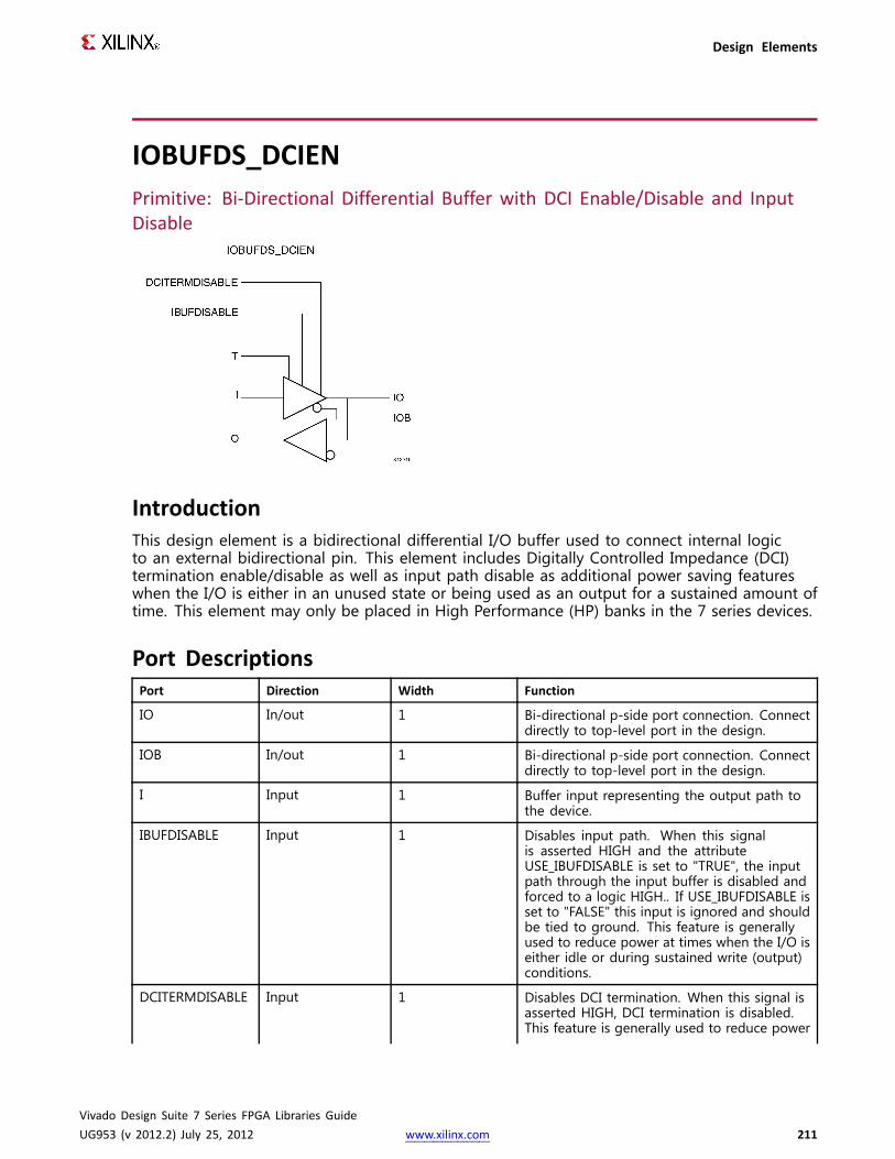
Design Elements
IOBUFDS_DCIENPrimitive: Bi-Directional Differential Buffer with DCI Enable/Disable and InputDisable
IntroductionThis design element is a bidirectional differential I/O buffer used to connect internal logicto an external bidirectional pin. This element includes Digitally Controlled Impedance (DCI)termination enable/disable as well as input path disable as additional power saving featureswhen the I/O is either in an unused state or being used as an output for a sustained amount oftime. This element may only be placed in High Performance (HP) banks in the 7 series devices.
Port DescriptionsPort Direction Width Function
IO In/out 1 Bi-directional p-side port connection. Connectdirectly to top-level port in the design.
IOB In/out 1 Bi-directional p-side port connection. Connectdirectly to top-level port in the design.
I Input 1 Buffer input representing the output path tothe device.
IBUFDISABLE Input 1 Disables input path. When this signalis asserted HIGH and the attributeUSE_IBUFDISABLE is set to "TRUE", the inputpath through the input buffer is disabled andforced to a logic HIGH.. If USE_IBUFDISABLE isset to "FALSE" this input is ignored and shouldbe tied to ground. This feature is generallyused to reduce power at times when the I/O iseither idle or during sustained write (output)conditions.
DCITERMDISABLE Input 1 Disables DCI termination. When this signal isasserted HIGH, DCI termination is disabled.This feature is generally used to reduce power
Vivado Design Suite 7 Series FPGA Libraries GuideUG953 (v 2012.2) July 25, 2012 www.xilinx.com 211

Design Elements
Port Direction Width Functionat times when the I/O is either idle or duringsustained write (output) conditions.
T Input 1 Sets the I/O in a high impedance 3-statemode when the I/O is being used for a read(input) operation. The T pin also affects theIBUFDISABLE function when USE_IBUFDISABLE= "TRUE".
O Output 1 Buffer output representing the input path tothe device.
Design Entry MethodInstantiation Yes
Inference No
CORE Generator™ and wizards Yes
Macro support No
Available Attributes
AttributeDataType Allowed Values Default Description
DIFF_TERM String "TRUE", "FALSE" "FALSE" Enable the built-in differentialtermination.
IBUF_LOW_PWR
String "TRUE", "FALSE" "TRUE" Allows a trade off of lowerpower consumption vs. highestperformance.
IOSTANDARD String See Data Sheet "DEFAULT" Assigns an I/O standard to theelement.
SLEW String "SLOW", "FAST", "SLOW" Sets the output rise and falltime. See the Data Sheet forrecommendations of the bestsetting for this attribute.
USE_IBUFDISABLE
String "TRUE", "FALSE" "TRUE" Enables or disables the feature ofIBUFDISABLE. Set to FALSE when itis not desirable to have the T pindisable input path to allow a readduring write operation. When setto TRUE deasserting T (IO used asoutput) or asserting IBUFDISABLEwill disable the input path throughthe buffer and forces to a logichigh.
Vivado Design Suite 7 Series FPGA Libraries GuideUG953 (v 2012.2) July 25, 2012 www.xilinx.com 212

Design Elements
VHDL Instantiation TemplateUnless they already exist, copy the following two statements and paste them before the entitydeclaration.Library UNISIM;use UNISIM.vcomponents.all;
-- IOBUFDS_DCIEN: Differential Bi-directional Buffer with Digital Controlled Impedance (DCI)-- and Input path enable/disable-- May only be placed in High Performance (HP) Banks-- 7 Series-- Xilinx HDL Libraries Guide, version 2012.2
IOBUFDS_DCIEN_inst : IOBUFDS_DCIENgeneric map (
DIFF_TERM => "FALSE", -- Differential termination (TRUE/FALSE)IBUF_LOW_PWR=> "TRUE", -- Low Power - TRUE, HIGH Performance = FALSEIOSTANDARD=> "BLVDS_25", -- Specify the I/O standardSLEW=> "SLOW", -- Specify the output slew rateUSE_IBUFDISABLE => "TRUE") -- Use IBUFDISABLE function "TRUE" or "FALSE"
port map (O => O, -- Buffer outputIO => IO, -- Diff_p inout (connect directly to top-level port)IOB => IOB, -- Diff_n inout (connect directly to top-level port)DCITERMDISABLE => DCITERMDISABLE, -- DCI Termination enable inputI => I, -- Buffer inputIBUFDISABLE => IBUFDISABLE, -- Input disable input, low=disableT => T -- 3-state enable input, high=input, low=output
);
-- End of IOBUFDS_DCIEN_inst instantiation
Verilog Instantiation Template
// IOBUFDS_DCIEN: Differential Bi-directional Buffer with Digital Controlled Impedance (DCI)// and Input path enable/disable// May only be placed in High Perforrmance (HP) Banks// 7 Series// Xilinx HDL Libraries Guide, version 2012.2
IOBUFDS_DCIEN #(.DIFF_TERM("FALSE"), // Differential Termination ("TRUE"/"FALSE").IBUF_LOW_PWR("TRUE"), // Low Power - "TRUE", High Perforrmance = "FALSE".IOSTANDARD("BLVDS_25"), // Specify the I/O standard.SLEW("SLOW"), // Specify the output slew rate.USE_IBUFDISABLE("TRUE") // Use IBUFDISABLE function, "TRUE" or "FALSE"
) IOBUFDS_DCIEN_inst (.O(O), // Buffer output.IO(IO), // Diff_p inout (connect directly to top-level port).IOB(IOB), // Diff_n inout (connect directly to top-level port).DCITERMDISABLE(DCITERMDISABLE), // DCI Termination enable input.I(I), // Buffer input.IBUFDISABLE(IBUFDISABLE), // Input disable input, low=disable.T(T) // 3-state enable input, high=input, low=output
);
// End of IOBUFDS_DCIEN_inst instantiation
For More Information• See the 7 series FPGA SelectIO Resources User Guide (UG471).
• See the 7 series FPGA User Documentation (User Guides and Data Sheets).
Vivado Design Suite 7 Series FPGA Libraries GuideUG953 (v 2012.2) July 25, 2012 www.xilinx.com 213
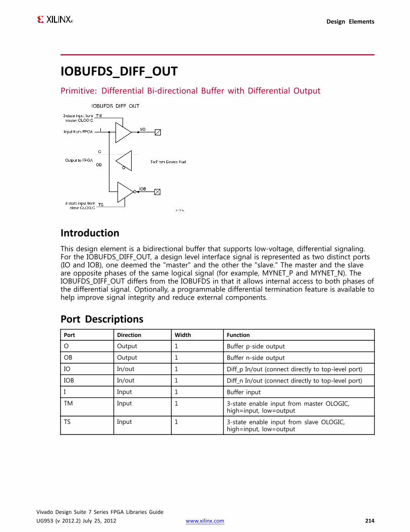
Design Elements
IOBUFDS_DIFF_OUTPrimitive: Differential Bi-directional Buffer with Differential Output
IntroductionThis design element is a bidirectional buffer that supports low-voltage, differential signaling.For the IOBUFDS_DIFF_OUT, a design level interface signal is represented as two distinct ports(IO and IOB), one deemed the "master" and the other the "slave." The master and the slaveare opposite phases of the same logical signal (for example, MYNET_P and MYNET_N). TheIOBUFDS_DIFF_OUT differs from the IOBUFDS in that it allows internal access to both phases ofthe differential signal. Optionally, a programmable differential termination feature is available tohelp improve signal integrity and reduce external components.
Port DescriptionsPort Direction Width Function
O Output 1 Buffer p-side output
OB Output 1 Buffer n-side output
IO In/out 1 Diff_p In/out (connect directly to top-level port)
IOB In/out 1 Diff_n In/out (connect directly to top-level port)
I Input 1 Buffer input
TM Input 1 3-state enable input from master OLOGIC,high=input, low=output
TS Input 1 3-state enable input from slave OLOGIC,high=input, low=output
Vivado Design Suite 7 Series FPGA Libraries GuideUG953 (v 2012.2) July 25, 2012 www.xilinx.com 214

Design Elements
Design Entry MethodInstantiation Recommended
Inference No
CORE Generator™ and wizards No
Macro support No
Available Attributes
AttributeDataType Allowed Values Default Description
DIFF_TERM Boolean TRUE, FALSE FALSE The differential terminationattribute is designed for the 7Series FPGA supported differentialinput I/O standards. It is used toturn the built-in, 100?, differentialtermination on (TRUE) or off(FALSE).
IBUF_LOW_PWR Boolean TRUE, FALSE TRUE When set to TRUE, allows forreduced power when usingdifferential or referenced (requiringVREF) input standards like LVDSor HSTL. A setting of FALSEdemands more power but delivershigher performance characteristics.Consult the 7 Series FPGA SelectIOResources User Guide for details.
IOSTANDARD String See Data Sheet "DEFAULT" Assigns an I/O standard to theelement.
VHDL Instantiation TemplateUnless they already exist, copy the following two statements and paste them before the entitydeclaration.Library UNISIM;use UNISIM.vcomponents.all;
-- IOBUFDS_DIFF_OUT: Differential Bi-directional Buffer with Differential Output-- 7 Series-- Xilinx HDL Libraries Guide, version 2012.2
IOBUFDS_DIFF_OUT_inst : IOBUFDS_DIFF_OUTgeneric map (
DIFF_TERM => FALSE, -- Differential Termination (TRUE/FALSE)IBUF_LOW_PWR=> TRUE, -- Low Power - TRUE, High Performance = FALSEIOSTANDARD=> "BLVDS_25") -- Specify the I/O standard
port map (O => O, -- Buffer p-side outputOB => OB, -- Buffer n-side outputIO => IO, -- Diff_p inout (connect directly to top-level port)IOB => IOB, -- Diff_n inout (connect directly to top-level port)I => I, -- Buffer inputTM => TM, -- 3-state enable input, high=input, low=outputTS => TS -- 3-state enable input, high=output, low=input
);
Vivado Design Suite 7 Series FPGA Libraries GuideUG953 (v 2012.2) July 25, 2012 www.xilinx.com 215

Design Elements
-- End of IOBUFDS_DIFF_OUT_inst instantiation
Verilog Instantiation Template
// IOBUFDS_DIFF_OUT: Differential Bi-directional Buffer with Differential Output// 7 Series// Xilinx HDL Libraries Guide, version 2012.2
IOBUFDS_DIFF_OUT #(.DIFF_TERM("FALSE"), // Differential Termination ("TRUE"/"FALSE").IBUF_LOW_PWR("TRUE"), // Low Power - "TRUE", High Perforrmance = "FALSE".IOSTANDARD("BLVDS_25") // Specify the I/O standard
) IOBUFDS_DIFF_OUT_inst (.O(O), // Buffer p-side output.OB(OB), // Buffer n-side output.IO(IO), // Diff_p inout (connect directly to top-level port).IOB(IOB), // Diff_n inout (connect directly to top-level port).I(I), // Buffer input.TM(TM), // 3-state enable input, high=input, low=output.TS(TS) // 3-state enable input, high=output, low=input
);
// End of IOBUFDS_DIFF_OUT_inst instantiation
For More Information• See the 7 series FPGA SelectIO Resources User Guide (UG471).
• See the 7 series FPGA User Documentation (User Guides and Data Sheets).
Vivado Design Suite 7 Series FPGA Libraries GuideUG953 (v 2012.2) July 25, 2012 www.xilinx.com 216

Design Elements
IOBUFDS_DIFF_OUT_DCIENPrimitive: Bi-Directional Differential Buffer with DCI Disable, Input Disable, andDifferential Output
IntroductionThis design element is a bidirectional differential I/O buffer used to connect internal logicto an external bidirectional pin. This element includes Digitally Controlled Impedance (DCI)termination enable/ disable as well as input path disable as additional power saving featureswhen the I/O is either is an unused state or being used as an output for a sustained amount oftime. The IOBUFDS_DIFF_OUT_DCIEN differs from the IOBUFDS_DCIEN in that it allows internalaccess to both phases of the differential signal. This element may only be placed in HighPerformance (HP) banks in the 7 series devices.
Port DescriptionsPort Direction Width Function
IO In/out 1 Bi-directional p-side port connection. Connectdirectly to top-level port in the design.
IOB In/out 1 Bi-directional n-side port connection. Connectdirectly to top-level port in the design.
I Input 1 Buffer input representing the output path tothe device.
IBUFDISABLE Input 1 Disables input path. When this signalis asserted HIGH and the attributeUSE_IBUFDISABLE is set to "TRUE", the inputpath through the input buffer is disabled andforced to a logic HIGH.. If USE_IBUFDISABLEis set to "FALSE" this input is ignored andshould be tied to ground. This feature isgenerally used to reduce power at times whenthe I/O is either idle or during sustained write(output) conditions.
Vivado Design Suite 7 Series FPGA Libraries GuideUG953 (v 2012.2) July 25, 2012 www.xilinx.com 217
Design Elements
Port Direction Width Function
DCITERMDISABLE Input 1 Disables DCI termination. When this signal isasserted HIGH, DCI termination is disabled.This feature is generally used to reduce powerat times when the I/O is either idle or duringsustained write (output) conditions.
TM Input 1 P-side or master side of the high impedance3-state mode when the I/O is being usedfor a read (input) operation. The TM pinalso affects the IBUFDISABLE function whenUSE_IBUFDISABLE = "TRUE".
TS Input 1 N-side or slave side of the high impedance3-state mode when the I/O is being usedfor a read (input) operation. The TM pinalso affects the IBUFDISABLE function whenUSE_IBUFDISABLE = "TRUE".
O Output 1 Buffer p-side output representing the inputpath to the device.
OB Output 1 Buffer n-side output representing the inputpath to the device.
Design Entry MethodInstantiation Yes
Inference No
CORE Generator™ and wizards Yes
Macro support No
Available Attributes
AttributeDataType Allowed Values Default Description
DIFF_TERM String "TRUE", "FALSE" "FALSE" Enable the built-in differentialtermination.
IBUF_LOW_PWR
String "TRUE", "FALSE" "TRUE" Allows a trade off of lowerpower consumption vs highestperformance.
IOSTANDARD String See Data Sheet "DEFAULT" Assigns an I/O standard to theelement.
USE_IBUFDISABLE
String "TRUE", "FALSE" "TRUE" Enables or disables the feature ofIBUFDISABLE. Set to FALSE when itis not desirable to have the T pindisable input path to allow a readduring write operation. When setto TRUE deasserting T (IO used asoutput) or asserting IBUFDISABLEwill disable the input path throughthe buffer and forces to a logichigh.
Vivado Design Suite 7 Series FPGA Libraries GuideUG953 (v 2012.2) July 25, 2012 www.xilinx.com 218

Design Elements
VHDL Instantiation TemplateUnless they already exist, copy the following two statements and paste them before the entitydeclaration.Library UNISIM;use UNISIM.vcomponents.all;
-- IOBUFDS_DIFF_OUT_DCIEN: Differential Bi-directional Buffer with Differential Output,-- Digital Controlled Impedance (DCI)and Input path enable/disable-- May only be placed in High Performance (HP) Banks-- 7 Series-- Xilinx HDL Libraries Guide, version 2012.2
IOBUFDS_DIFF_OUT_DCIEN_inst : IOBUFDS_DIFF_OUT_DCIENgeneric map (
DIFF_TERM => "FALSE", -- Differential Termination (TRUE/FALSE)IBUF_LOW_PWR=> "TRUE", -- Low Power - TRUE, High Performance = FALSEIOSTANDARD=> "BLVDS_25", -- Specify the I/O standardUSE_IBUFDISABLE => "TRUE") -- Use IBUFDISABLE function, "TRUE" or "FALSE"
port map (O => O, -- Buffer p-side outputOB => OB, -- Buffer n-side outputIO => IO, -- Diff_p inout (connect directly to top-level port)IOB => IOB, -- Diff_n inout (connect directly to top-level port)DCITERMDISABLE => DCITERMDISABLE, -- DCI Termination enable inputI => I, -- Buffer inputIBUFTERMDISABLE => IBUFTERMDISABLE, -- input disable input, low=disableTM => TM, -- 3-state enable input, high=input, low=outputTS => TS -- 3-state enable input, high=output, low=input
);
-- End of IOBUFDS_DIFF_OUT_DCIEN_inst instantiation
Verilog Instantiation Template
// IOBUFDS_DIFF_OUT_DCIEN: Differential Bi-directional Buffer with Differential Output,// Digital Controlled Impedance (DCI)and Input path enable/disable// May only be placed in High Perforrmance (HP) Banks// 7 Series// Xilinx HDL Libraries Guide, version 2012.2
IOBUFDS_DIFF_OUT_DCIEN #(.DIFF_TERM("FALSE"), // Differential Termination ("TRUE"/"FALSE").IBUF_LOW_PWR("TRUE"), // Low Power - "TRUE", High Perforrmance = "FALSE".IOSTANDARD("BLVDS_25"), // Specify the I/O standard.USE_IBUFDISABLE("TRUE") // Use IBUFDISABLE function, "TRUE" or "FALSE"
) IOBUFDS_DIFF_OUT_DCIEN_inst (.O(O), // Buffer p-side output.OB(OB), // Buffer n-side output.IO(IO), // Diff_p inout (connect directly to top-level port).IOB(IOB), // Diff_n inout (connect directly to top-level port).DCITERMDISABLE(DCITERMDISABLE), // DCI Termination enable input.I(I), // Buffer input.IBUFDISABLE(IBUFDISABLE), // Input disable input, low=disable.TM(TM), // 3-state enable input, high=input, low=output.TS(TS) // 3-state enable input, high=output, low=input
);
// End of IOBUFDS_DIFF_OUT_DCIEN_inst instantiation
For More Information• See the 7 series FPGA SelectIO Resources User Guide (UG471).• See the 7 series FPGA User Documentation (User Guides and Data Sheets).
Vivado Design Suite 7 Series FPGA Libraries GuideUG953 (v 2012.2) July 25, 2012 www.xilinx.com 219

Design Elements
IOBUFDS_DIFF_OUT_INTERMDISABLEPrimitive: Bi-Directional Differential Buffer with Input Termination Disable, InputDisable, and Differential Output
IntroductionThis design element is a bidirectional differential I/O Buffer used to connect internal logicto an external bidirectional pin. This element includes an uncalibrated input termination(INTERM) disable as well as input path disable as additional power saving features when theI/O is either is an unused state or being used as an output for several clock cycles. TheIOBUFDS_DIFF_OUT_INTERMDISABLE differs from the IOBUFDS_INTERMDISABLE in that it allowsinternal access to both phases of the differential signal. This element may only be placed inHigh Range (HR) banks in the 7 series devices.
Port DescriptionsPort Direction Width Function
IO In/out 1 Bi-directional p-side port connection. Connectdirectly to top-level port in the design.
IOB In/out 1 Bi-directional n-side port connection. Connectdirectly to top-level port in the design.
I Input 1 Buffer input representing the output path to thedevice.
IBUFDISABLE Input 1 Disables input path through the buffer and forcesto a logic high when USE_IBUFDISABLE is set to"TRUE". If USE_IBUFDISABLE is set to "FALSE" thisinput is ignored and should be tied to ground. Thisfeature is generally used to reduce power at timeswhen the I/O is either idle or during sustainedwrite (output) conditions.
INTERMDISABLE Input 1 Disables input termination. This feature is generallyused to reduce power at times when the I/O
Vivado Design Suite 7 Series FPGA Libraries GuideUG953 (v 2012.2) July 25, 2012 www.xilinx.com 220

Design Elements
Port Direction Width Functionis either idle or during sustained write (output)conditions.
TM Input 1 P-side or master side of the high impedance3-state mode when the I/O is being used for aread (input) operation. The TM pin also affectsthe IBUFDISABLE function when USE_IBUFDISABLE= "TRUE", and disables INTERM when in a write(output) mode.
TS Input 1 N-side or slave side of the high impedance 3-statemode when the I/O is being used for a read (input)operation. The TS pin also affects the IBUFDISABLEfunction when USE_IBUFDISABLE = "TRUE", anddisables INTERM when in a write (output) mode.
O Output 1 Buffer p-side output representing the input pathto the device.
OB Output 1 Buffer n-side output representing the input pathto the device.
Design Entry MethodInstantiation Yes
Inference No
CORE Generator™ and wizards Yes
Macro support No
Available Attributes
AttributeDataType Allowed Values Default Description
DIFF_TERM String "TRUE", "FALSE" "FALSE" Enable the built-in differentialtermination.
IBUF_LOW_PWR String "TRUE", "FALSE" "TRUE" Allows a trade off of lowerpower consumption vs. highestperformance when referenced I/Ostandards are used.
IOSTANDARD String See Data Sheet "DEFAULT" Assigns an I/O standard to theelement.
USE_IBUFDISABLE String "TRUE", "FALSE" "TRUE" Enables or disables the feature ofIBUFDISABLE. Generally used whenit is not desirable to have the T pindisable input path to allow a readduring write operation.
Vivado Design Suite 7 Series FPGA Libraries GuideUG953 (v 2012.2) July 25, 2012 www.xilinx.com 221
Design Elements
VHDL Instantiation TemplateUnless they already exist, copy the following two statements and paste them before the entitydeclaration.Library UNISIM;use UNISIM.vcomponents.all;
-- IOBUFDS_DIFF_OUT_INTERMDISABLE: Differential Global Clock Buffer with Differential Output-- Input Termination and Input Path Disable-- May only be placed in High Range (HR) Banks-- 7 Series-- Xilinx HDL Libraries Guide, version 2012.2
IOBUFDS_DIFF_OUT_INTERMDISABLE_inst : IOBUFDS_DIFF_OUT_INTERMDISABLEgeneric map (
DIFF_TERM => "FALSE", -- Differential Termination (TRUE/FALSE)IBUF_LOW_PWR=> "TRUE", -- Low Power - TRUE, High Performance = FALSEIOSTANDARD=> "BLVDS_25", -- Specify the I/O standardUSE_IBUFDISABLE => "TRUE") -- Use IBUFDISABLE function, "TRUE" or "FALSE"
port map (O => O, -- Buffer p-side outputOB => OB, -- Buffer n-side outputIO => IO, -- Diff_p inout (connect directly to top-level port)IOB => IOB, -- Diff_n inout (connect directly to top-level port)DCITERMDISABLE => DCITERMDISABLE, -- DCI Termination enable inputI => I, -- Buffer inputIBUFDISABLE => IBUFDISABLE, -- input disable input, low=disableINTERMDISABLE => INTERMDISABLE, -- Input termination disable inputTM => TM, -- 3-state enable input, high=input, low=outputTS => TS -- 3-state enable input, high=output, low=input
);
-- End of IOBUFDS_DIFF_OUT_INTERMDISABLE_inst instantiation
Verilog Instantiation Template
// IOBUFDS_DIFF_OUT_INTERMDISABLE: Differential Global Clock Buffer with Differential Output// Input Termination and Input Path Disable// May only be placed in High Range (HR) Banks// 7 Series// Xilinx HDL Libraries Guide, version 2012.2
IOBUFDS_DIFF_OUT_INTERMDISABLE#(.DIFF_TERM("FALSE"), // Differential Termination, "TRUE"/"FALSE".IBUF_LOW_PWR("TRUE"), // Low power="TRUE", Highest perforrmance="FALSE".IOSTANDARD("DEFAULT"), // Specify the input I/O standard.USE_IBUFDISABLE("TRUE") // Set to "TRUE" to enable IBUFDISABLE feature
) IOBUFDS_DIFF_OUT_INTERMDISABLE_inst (.O(O), // Buffer p-side output.OB(OB), // Buffer n-side output.IO(IO), // Diff_p inout (connect directly to top-level port).IOB(IOB), // Diff_n inout (connect directly to top-level port).I(I), // Buffer input.INTERMDISABLE(INTERMDISABLE), // Input termination disable input.IBUFDISABLE(IBUFDISABLE), // Input disable input, low=disable.TM(TM), // 3-state enable input, high=input, low=output.TS(TS) // 3-state enable input, high=output, low=input
);
// End of IOBUFDS_DIFF_OUT_INTERMDISABLE_inst instantiation
Vivado Design Suite 7 Series FPGA Libraries GuideUG953 (v 2012.2) July 25, 2012 www.xilinx.com 222

Design Elements
For More Information• See the 7 series FPGA SelectIO Resources User Guide (UG471).
• See the 7 series FPGA User Documentation (User Guides and Data Sheets).
Vivado Design Suite 7 Series FPGA Libraries GuideUG953 (v 2012.2) July 25, 2012 www.xilinx.com 223
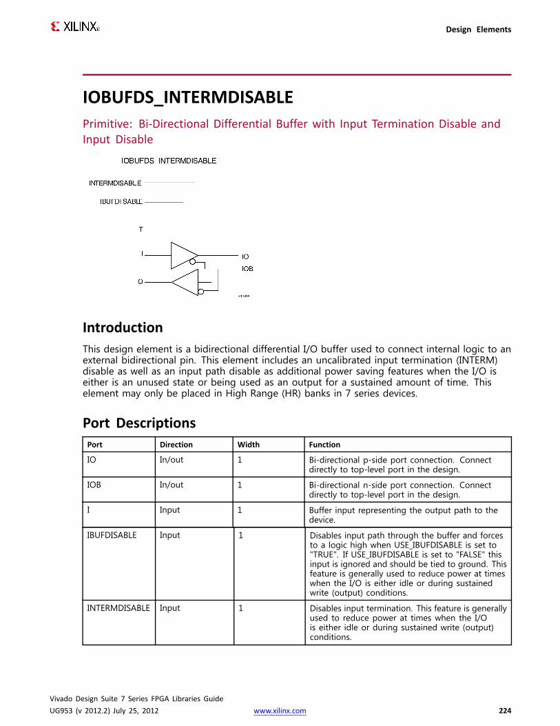
Design Elements
IOBUFDS_INTERMDISABLEPrimitive: Bi-Directional Differential Buffer with Input Termination Disable andInput Disable
IntroductionThis design element is a bidirectional differential I/O buffer used to connect internal logic to anexternal bidirectional pin. This element includes an uncalibrated input termination (INTERM)disable as well as an input path disable as additional power saving features when the I/O iseither is an unused state or being used as an output for a sustained amount of time. Thiselement may only be placed in High Range (HR) banks in 7 series devices.
Port DescriptionsPort Direction Width Function
IO In/out 1 Bi-directional p-side port connection. Connectdirectly to top-level port in the design.
IOB In/out 1 Bi-directional n-side port connection. Connectdirectly to top-level port in the design.
I Input 1 Buffer input representing the output path to thedevice.
IBUFDISABLE Input 1 Disables input path through the buffer and forcesto a logic high when USE_IBUFDISABLE is set to"TRUE". If USE_IBUFDISABLE is set to "FALSE" thisinput is ignored and should be tied to ground. Thisfeature is generally used to reduce power at timeswhen the I/O is either idle or during sustainedwrite (output) conditions.
INTERMDISABLE Input 1 Disables input termination. This feature is generallyused to reduce power at times when the I/Ois either idle or during sustained write (output)conditions.
Vivado Design Suite 7 Series FPGA Libraries GuideUG953 (v 2012.2) July 25, 2012 www.xilinx.com 224
Design Elements
T Input 1 Sets the I/O in a high impedance 3-state modewhen the I/O is being used for a read (input)operation. The T pin also affects the IBUFDISABLEfunction when USE_IBUFDISABLE = "TRUE". The Tpin also disables INTERM when in a write (output)mode.
O Output 1 Buffer output representing the input path to thedevice.
Design Entry MethodInstantiation Yes
Inference No
CORE Generator™ and wizards Yes
Macro support No
Available Attributes
AttributeDataType Allowed Values Default Description
DIFF_TERM String "TRUE", "FALSE" "FALSE" Enable the built-in differentialtermination.
IBUF_LOW_PWR String "TRUE", "FALSE" "TRUE" Allows a trade off of lowerpower consumption vs. highestperformance when referenced I/Ostandards are used.
IOSTANDARD String See Data Sheet "DEFAULT" Assigns an I/O standard to theelement.
SLEW String "SLOW" or"FAST"
"SLOW" Sets the output rise and falltime. See the Data Sheet forrecommendations of the bestsetting for this attribute.
USE_IBUFDISABLE String "TRUE", "FALSE" "TRUE" Enables or disables the feature ofIBUFDISABLE. Generally used whenit is not desirable to have the T pindisable input path to allow a readduring write operation.
VHDL Instantiation TemplateUnless they already exist, copy the following two statements and paste them before the entitydeclaration.Library UNISIM;use UNISIM.vcomponents.all;
-- IOBUFDS_INTERMDISABLE: Differential Bi-directional Buffer with Input Termination-- and Input path enable/disable-- May only be placed in High Range (HR) Banks-- 7 Series-- Xilinx HDL Libraries Guide, version 2012.2
Vivado Design Suite 7 Series FPGA Libraries GuideUG953 (v 2012.2) July 25, 2012 www.xilinx.com 225

Design Elements
IOBUFDS_INTERMDISABLE_inst : IOBUFDS_INTERMDISABLEgeneric map (
DIFF_TERM => "FALSE", -- Differential termination (TRUE/FALSE)IBUF_LOW_PWR=> "TRUE", -- Low Power - TRUE, HIGH Performance = FALSEIOSTANDARD=> "BLVDS_25", -- Specify the I/O standardSLEW=> "SLOW", -- Specify the output slew rateUSE_IBUFDISABLE => "TRUE") -- Use IBUFDISABLE function "TRUE" or "FALSE"
port map (O => O, -- Buffer outputIO => IO, -- Diff_p inout (connect directly to top-level port)IOB => IOB, -- Diff_n inout (connect directly to top-level port)DCITERMDISABLE => DCITERMDISABLE, -- DCI Termination enable inputI => I, -- Buffer inputIBUFDISABLE => IBUFDISABLE, -- Input disable input, low=disableINTERMDISABLE => INTERMDISABLE, -- Input termination disable inputT => T -- 3-state enable input, high=input, low=output
);
-- End of IOBUFDS_INTERMDISABLE_inst instantiation
Verilog Instantiation Template
// IOBUFDS_INTERMDISABLE: Differential Bi-directional Buffer with Input Termination// and Input path enable/disable// May only be placed in High Range (HR) Banks// 7 Series// Xilinx HDL Libraries Guide, version 2012.2
IOBUFDS_INTERMDISABLE#(.DIFF_TERM("FALSE"), // Differential Termination ("TRUE"/"FALSE").IBUF_LOW_PWR("TRUE"), // Low Power - "TRUE", High Perforrmance = "FALSE".IOSTANDARD("BLVDS_25"), // Specify the I/O standard.SLEW("SLOW"), // Specify the output slew rate.USE_IBUFDISABLE("TRUE") // Use IBUFDISABLE function, "TRUE" or "FALSE"
) IOBUFDS_INTERMDISABLE_inst (.O(O), // Buffer output.IO(IO), // Diff_p inout (connect directly to top-level port).IOB(IOB), // Diff_n inout (connect directly to top-level port).I(I), // Buffer input.IBUFDISABLE(IBUFDISABLE), // Input disable input, low=disable.INTERMDISABLE(INTERMDISABLE), // Input termination disable input.T(T) // 3-state enable input, high=input, low=output
);
// End of IOBUFDS_INTERMDISABLE_inst instantiation
For More Information• See the 7 series FPGA SelectIO Resources User Guide (UG471).
• See the 7 series FPGA User Documentation (User Guides and Data Sheets).
Vivado Design Suite 7 Series FPGA Libraries GuideUG953 (v 2012.2) July 25, 2012 www.xilinx.com 226

Design Elements
ISERDESE2Primitive: Input SERial/DESerializer with bitslip
IntroductionThe ISERDESE2 in 7 series FPGAs is a dedicated serial-to-parallel converter with specific clockingand logic features designed to facilitate the implementation of high-speed source-synchronousapplications. The ISERDESE2 avoids the additional timing complexities encountered whendesigning deserializers in the FPGA fabric. ISERDESE2 features include:
• Dedicated Deserializer/Serial-to-Parallel Converter, which enables high-speed datatransfer without requiring the FPGA fabric to match the input data frequency. Thisconverter supports both single data rate (SDR) and double data rate (DDR) modes. InSDR mode, the serial-to-parallel converter creates a 2-, 3-, 4-, 5-, 6-, 7-, or 8-bit wideparallel word. In DDR mode, the serial-to-parallel converter creates a 4-, 6-, 8-, 10-, or14-bit-wide parallel word.
• Bitslip Submodule, which lets designers reorder the sequence of the parallel data streamgoing into the FPGA fabric. This can be used for training source-synchronous interfacesthat include a training pattern.
• Dedicated Support for Strobe-based Memory Interfaces, including the OCLK input pin,to handle the strobe-to-FPGA clock domain crossover entirely within the ISERDESE2block. This allows for higher performance and a simplified implementation.
• Dedicated Support for Networking Interfaces
• Dedicated Support for Memory Interfaces
Vivado Design Suite 7 Series FPGA Libraries GuideUG953 (v 2012.2) July 25, 2012 www.xilinx.com 227

Design Elements
Port DescriptionsPort Type Width Function
BITSLIP Input 1 The BITSLIP pin performs a Bitslip operation synchronousto CLKDIV when asserted (active High). Subsequently, thedata seen on the Q1 to Q8 output ports will shift, as in abarrel-shifter operation, one position every time Bitslip isinvoked (DDR operation is different from SDR).
CE1, CE2 Input 1 Each ISERDESE2 block contains an input clock enable module.When NUM_CE = 1, the CE2 input is not used, and the CE1input is an active high clock enable connected directly to theinput registers in the ISERDESE2. When NUM_CE = 2, the CE1and CE2 inputs are both used, with CE1 enabling the ISERDESE2for half of a CLKDIV cycle, and CE2 enabling the ISERDESE2for the other half. The clock enable module functions as a2:1 serial-to-parallel converter, clocked by CLKDIV. The clockenable module is needed specifically for bidirectional memoryinterfaces when ISERDESE2 is configured for 1:4 deserializationin DDR mode. When the attribute NUM_CE = 2, the clockenable module is enabled and both CE1 and CE2 ports areavailable. When NUM_CE = 1, only CE1 is available andfunctions as a regular clock enable.
CLK Input 1 The high-speed clock input (CLK) is used to clock in the inputserial data stream.
CLKB Input 1 The high-speed secondary clock input (CLKB) is used to clockin the input serial data stream. In any mode other than"MEMORY_QDR", connect CLKB to an inverted version of CLK.In "MEMORY_QDR" mode CLKB should be connected to aunique, phase shifted clock.
CLKDIV Input 1 The divided clock input (CLKDIV) is typically a dividedversion of CLK (depending on the width of the implementeddeserialization). It drives the output of the serial-to-parallelconverter, the Bitslip submodule, and the CE module.
CLKDIVP Input 1 Only supported in MIG. Sourced by PHASER_IN divided CLK inMEMORY_DDR3 mode. All other modes connect to ground.
D Input 1 The serial input data port (D) is the serial (high-speed) datainput port of the ISERDESE2. This port works in conjunctiononly with the 7 series FPGA I/O resource.
DDLY Input 1 The serial input data port (DDLY) is the serial (high-speed) datainput port of the ISERDESE2. This port works in conjunctiononly with the 7 series FPGA IDELAYE2 resource.
DYNCLKDIVSEL Input 1 Dynamically select CLKDIV inversion.
DYNCLKSEL Input 1 Dynamically select CLK and CLKB inversion.
O Output 1 The combinatorial output port (O) is an unregistered output ofthe ISERDESE2 module. This output can come directly from thedata input (D), or from the data input (DDLY) via the IDELAYE2.
Vivado Design Suite 7 Series FPGA Libraries GuideUG953 (v 2012.2) July 25, 2012 www.xilinx.com 228

Design Elements
Port Type Width Function
OCLK Input 1 The OCLK clock input synchronizes data transfer instrobe-based memory interfaces. The OCLK clock is only usedwhen INTERFACE_TYPE is set to "MEMORY". The OCLK clockinput is used to transfer strobe-based memory data onto afree-running clock domain. OCLK is a free-running FPGA clockat the same frequency as the strobe on the CLK input. Thetiming of the domain transfer is set by the user by adjustingthe delay of the strobe signal to the CLK input (e.g., usingIDELAY). Examples of setting the timing of this domain transferare given in the Memory Interface Generator (MIG). WhenINTERFACE_TYPE is "NETWORKING", this port is unused andshould be connected to GND.
OCLKB Input 1 The OCLK clock input synchronizes data transfer instrobe-based memory interfaces. The OCLKB clock is only usedwhen INTERFACE_TYPE is set to "MEMORY".
OFB Input 1 The serial input data port (OFB) is the serial (high-speed) datainput port of the ISERDESE2. This port works in conjunctiononly with the 7 series FPGA OSERDESE2 port OFB.
Q1 - Q8 Output 1 The output ports Q1 to Q8 are the registered outputs of theISERDESE2 module. One ISERDESE2 block can support up toeight bits (i.e., a 1:8 deserialization). Bit widths greater thaneight (up to 14) can be supported using Width Expansion. Thefirst data bit received appears on the highest order Q output.The bit ordering at the input of an OSERDESE2 is the oppositeof the bit ordering at the output of an ISERDESE2 block. Forexample, the least significant bit A of the word FEDCBA isplaced at the D1 input of an OSERDESE2, but the same bit Aemerges from the ISERDESE2 block at the Q8 output. In otherwords, D1 is the least significant input to the OSERDESE2,while Q8 is the least significant output of the ISERDESE2 block.When width expansion is used, D1 of the master OSERDESE1is the least significant input, while Q7 of the slave ISERDESE2block is the least significant output.
RST Input 1 The reset input causes the outputs of all data flip-flops in theCLK and CLKDIV domains to be driven low asynchronously.ISERDESE2 circuits running in the CLK domain where timing iscritical use an internal, dedicated circuit to retime the RST inputto produce a reset signal synchronous to the CLK domain.Similarly, there is a dedicated circuit to retime the RST inputto produce a reset signal synchronous to the CLKDIV domain.Because the ISERDESE2 is driven into reset asynchronouslybut comes out of reset synchronously it must be treated asa synchronous reset to the CLKDIV time domain and havea minimum pulse of one CLKDIV cycle. When building aninterface consisting of multiple ISERDESE2 ports, all ISERDESE2ports in the interface must be synchronized. The internalretiming of the RST input is designed so that all ISERDESE2blocks that receive the same reset pulse come out of resetsynchronized with one another.
SHIFTIN1-SHIFTIN2
Input 1 If SERDES_MODE="SLAVE", connect SHIFTIN1/2 to themaster ISERDESE2 SHIFTOUT1/2 outputs. Otherwise, leaveSHIFTOUT1/2 unconnected and/or SHIFTIN1/2 grounded.
SHIFTOUT1-SHIFTOUT2
Output 1 If SERDES_MODE="MASTER" and two ISERDESE2s are tobe cascaded, connect SHIFTOUT1/2 to the slave ISERDESE2SHIFTIN1/2 inputs.
Vivado Design Suite 7 Series FPGA Libraries GuideUG953 (v 2012.2) July 25, 2012 www.xilinx.com 229

Design Elements
Design Entry MethodInstantiation Yes
Inference No
CORE Generator™ and wizards Yes
Macro support No
Available AttributesAttribute Type Allowed Values Default Description
DATA_RATE STRING "DDR", "SDR" "DDR" The DATA_RATE attribute defineswhether the incoming data streamis processed as single data rate(SDR) or double data rate (DDR).
DATA_WIDTH DECIMAL 4, 2, 3, 5, 6, 7, 8, 10,14
4 Defines the width of theserial-to-parallel converter.The legal value depends on theDATA_RATE attribute (SDR or DDR).
• If DATA_RATE = DDR,value is limited to 4, 6, 8,10 or 14.
• If DATA_RATE = SDR, valueis limited to 2, 3, 4, 5, 6,7, or 8.
DYN_CLKDIV_INV_EN
STRING "FALSE", "TRUE" "FALSE" Enables DYNCLKDIVINVSELinversion when TRUE and disablesHDL inversions on CLKDIV pin.
DYN_CLK_INV_EN
STRING "FALSE", "TRUE" "FALSE" Enables DYNCLKINVSEL inversionwhen TRUE and disables HDLinversions on CLK and CLKB pins.
INIT_Q1,INIT_Q2,INIT_Q3,INIT_Q4
BINARY 1'b0 to 1'b1 1'b0 Defines the initial value on theQ1 through Q4 outputs afterconfiguration.
INTERFACE_TYPE
STRING "MEMORY","MEMORY_DDR3","MEMORY_QDR","NETWORKING","OVERSAMPLE"
"MEMORY" Specifies mode of operation forthe ISERDESE2. For details on eachmode, please refer to the 7 seriesFPGA SelectIO Resources UserGuide.
Vivado Design Suite 7 Series FPGA Libraries GuideUG953 (v 2012.2) July 25, 2012 www.xilinx.com 230

Design Elements
Attribute Type Allowed Values Default Description
IOBDELAY STRING "NONE", "BOTH","IBUF", "IFD"
"NONE" Defines input sources forISERDESE2 module. The D andDDLY pins are dedicated inputs tothe ISERDESE2. The D input is adirect connection to the I/O. TheDDLY pin is a direct connectionto the IODELAYE2. This allowsthe user to either have a delayedor non-delayed version of theinput to the registered (Q1- Q6) orcombinatorial path (O) output. Theattribute IOBDELAY determines theinput applied the output.
• "NONE" - O => D | Q1-Q6=> D
• "IBUF" - O => DDLY |Q1-Q6 => D
• "IFD" - O => D | Q1-Q6=> DDLY
• "BOTH" - O => DDLY |Q1-Q6 => DDLY
NUM_CE DECIMAL 2, 1 2 The NUM_CE attribute defines thenumber of clock enables (CE1 andCE2) used.
OFB_USED STRING "FALSE", "TRUE" "FALSE" Enables the path from the OLOGIC,OSERDES OFB pin to the ISERDESOFB pin. Disables the use of theD input pin.
SERDES_MODE STRING "MASTER", "SLAVE" "MASTER" The SERDES_MODE attributedefines whether the ISERDESE2module is a master or slave whenusing width expansion. Set to"MASTER" when not using widthexplansion.
SRVAL_Q1,SRVAL_Q2,SRVAL_Q3,SRVAL_Q4
BINARY 1'b0 to 1'b1 1'b0 Defines the value (set or reset) ofQ1 through Q4 outputs when theSR pin is invoked.
VHDL Instantiation TemplateUnless they already exist, copy the following two statements and paste them before the entitydeclaration.Library UNISIM;use UNISIM.vcomponents.all;
-- ISERDESE2: Input SERial/DESerializer with bitslip-- 7 Series-- Xilinx HDL Libraries Guide, version 2012.2
ISERDESE2_inst : ISERDESE2generic map (
DATA_RATE=> "DDR", -- DDR, SDR
Vivado Design Suite 7 Series FPGA Libraries GuideUG953 (v 2012.2) July 25, 2012 www.xilinx.com 231
Design Elements
DATA_WIDTH=> 4, -- Parallel data width (2-8,10,14)DYN_CLKDIV_INV_EN => "FALSE", -- Enable DYNCLKDIVINVSEL inversion (FALSE, TRUE)DYN_CLK_INV_EN => "FALSE", -- Enable DYNCLKINVSEL inversion (FALSE, TRUE)-- INIT_Q1 - INIT_Q4: Initial value on the Q outputs (0/1)INIT_Q1 => '0',INIT_Q2 => '0',INIT_Q3 => '0',INIT_Q4 => '0',INTERFACE_TYPE=> "MEMORY", -- MEMORY,MEMORY_DDR3,MEMORY_QDR,NETWORKING,OVERSAMPLEIOBDELAY => "NONE", -- NONE, BOTH, IBUF, IFDNUM_CE=> 2, -- Number of clock enables (1,2)OFB_USED=> "FALSE", -- Select OFB path (FALSE, TRUE)SERDES_MODE=> "MASTER", -- MASTER, SLAVE-- SRVAL_Q1 - SRVAL_Q4: Q output values when SR is used (0/1)SRVAL_Q1 => '0',SRVAL_Q2 => '0',SRVAL_Q3 => '0',SRVAL_Q4 => '0'
)port map (
O => O, -- 1-bit output: Combinatorial output-- Q1 - Q8: 1-bit (each) output: Registered data outputsQ1 => Q1,Q2 => Q2,Q3 => Q3,Q4 => Q4,Q5 => Q5,Q6 => Q6,Q7 => Q7,Q8 => Q8,-- SHIFTOUT1-SHIFTOUT2: 1-bit (each) output: Data width expansion output portsSHIFTOUT1 => SHIFTOUT1,SHIFTOUT2 => SHIFTOUT2,BITSLIP => BITSLIP, -- 1-bit input: The BITSLIP pin performs a Bitslip operation synchronous to
-- CLKDIV when asserted (active High). Subsequently, the data seen on the-- Q1 to Q8 output ports will shift, as in a barrel-shifter operation, one-- position every time Bitslip is invoked (DDR operation is different from-- SDR).
-- CE1, CE2: 1-bit (each) input: Data register clock enable inputsCE1 => CE1,CE2 => CE2,CLKDIVP => CLKDIVP, -- 1-bit input: TBD-- Clocks: 1-bit (each) input: ISERDESE2 clock input portsCLK => CLK, -- 1-bit input: High-speed clockCLKB => CLKB, -- 1-bit input: High-speed secondary clockCLKDIV => CLKDIV, -- 1-bit input: Divided clockOCLK => OCLK, -- 1-bit input: High speed output clock used when INTERFACE_TYPE="MEMORY"-- Dynamic Clock Inversions: 1-bit (each) input: Dynamic clock inversion pins to switch clock polarityDYNCLKDIVSEL => DYNCLKDIVSEL, -- 1-bit input: Dynamic CLKDIV inversionDYNCLKSEL=> DYNCLKSEL, -- 1-bit input: Dynamic CLK/CLKB inversion-- Input Data: 1-bit (each) input: ISERDESE2 data input portsD => D, -- 1-bit input: Data inputDDLY => DDLY, -- 1-bit input: Serial data from IDELAYE2OFB => OFB, -- 1-bit input: Data feedback from OSERDESE2OCLKB => OCLKB, -- 1-bit input: High speed negative edge output clockRST => RST, -- 1-bit input: Active high asynchronous reset-- SHIFTIN1-SHIFTIN2: 1-bit (each) input: Data width expansion input portsSHIFTIN1 => SHIFTIN1,SHIFTIN2 => SHIFTIN2
);
-- End of ISERDESE2_inst instantiation
Verilog Instantiation Template
// ISERDESE2: Input SERial/DESerializer with bitslip// 7 Series// Xilinx HDL Libraries Guide, version 2012.2
Vivado Design Suite 7 Series FPGA Libraries GuideUG953 (v 2012.2) July 25, 2012 www.xilinx.com 232

Design Elements
ISERDESE2 #(.DATA_RATE("DDR"), // DDR, SDR.DATA_WIDTH(4), // Parallel data width (2-8,10,14).DYN_CLKDIV_INV_EN("FALSE"), // Enable DYNCLKDIVINVSEL inversion (FALSE, TRUE).DYN_CLK_INV_EN("FALSE"), // Enable DYNCLKINVSEL inversion (FALSE, TRUE)// INIT_Q1 - INIT_Q4: Initial value on the Q outputs (0/1).INIT_Q1(1'b0),.INIT_Q2(1'b0),.INIT_Q3(1'b0),.INIT_Q4(1'b0),.INTERFACE_TYPE("MEMORY"), // MEMORY,MEMORY_DDR3,MEMORY_QDR,NETWORKING,OVERSAMPLE.IOBDELAY("NONE"), // NONE, BOTH, IBUF, IFD.NUM_CE(2), // Number of clock enables (1,2).OFB_USED("FALSE"), // Select OFB path (FALSE, TRUE).SERDES_MODE("MASTER"), // MASTER, SLAVE// SRVAL_Q1 - SRVAL_Q4: Q output values when SR is used (0/1).SRVAL_Q1(1'b0),.SRVAL_Q2(1'b0),.SRVAL_Q3(1'b0),.SRVAL_Q4(1'b0)
)ISERDESE2_inst (
.O(O), // 1-bit output: Combinatorial output// Q1 - Q8: 1-bit (each) output: Registered data outputs.Q1(Q1),.Q2(Q2),.Q3(Q3),.Q4(Q4),.Q5(Q5),.Q6(Q6),.Q7(Q7),.Q8(Q8),// SHIFTOUT1-SHIFTOUT2: 1-bit (each) output: Data width expansion output ports.SHIFTOUT1(SHIFTOUT1),.SHIFTOUT2(SHIFTOUT2),.BITSLIP(BITSLIP), // 1-bit input: The BITSLIP pin performs a Bitslip operation synchronous to
// CLKDIV when asserted (active High). Subsequently, the data seen on the Q1// to Q8 output ports will shift, as in a barrel-shifter operation, one// position every time Bitslip is invoked (DDR operation is different from// SDR).
// CE1, CE2: 1-bit (each) input: Data register clock enable inputs.CE1(CE1),.CE2(CE2),.CLKDIVP(CLKDIVP), // 1-bit input: TBD// Clocks: 1-bit (each) input: ISERDESE2 clock input ports.CLK(CLK), // 1-bit input: High-speed clock.CLKB(CLKB), // 1-bit input: High-speed secondary clock.CLKDIV(CLKDIV), // 1-bit input: Divided clock.OCLK(OCLK), // 1-bit input: High speed output clock used when INTERFACE_TYPE="MEMORY"// Dynamic Clock Inversions: 1-bit (each) input: Dynamic clock inversion pins to switch clock polarity.DYNCLKDIVSEL(DYNCLKDIVSEL), // 1-bit input: Dynamic CLKDIV inversion.DYNCLKSEL(DYNCLKSEL), // 1-bit input: Dynamic CLK/CLKB inversion// Input Data: 1-bit (each) input: ISERDESE2 data input ports.D(D), // 1-bit input: Data input.DDLY(DDLY), // 1-bit input: Serial data from IDELAYE2.OFB(OFB), // 1-bit input: Data feedback from OSERDESE2.OCLKB(OCLKB), // 1-bit input: High speed negative edge output clock.RST(RST), // 1-bit input: Active high asynchronous reset// SHIFTIN1-SHIFTIN2: 1-bit (each) input: Data width expansion input ports.SHIFTIN1(SHIFTIN1),.SHIFTIN2(SHIFTIN2)
);
// End of ISERDESE2_inst instantiation
For More Information• See the 7 series FPGA SelectIO Resources User Guide (UG471).• See the 7 series FPGA User Documentation (User Guides and Data Sheets).
Vivado Design Suite 7 Series FPGA Libraries GuideUG953 (v 2012.2) July 25, 2012 www.xilinx.com 233

Design Elements
KEEPERPrimitive: KEEPER Symbol
IntroductionThe design element is a weak keeper element that retains the value of the net connected toits bidirectional O pin. For example, if a logic 1 is being driven onto the net, KEEPER drives aweak/resistive 1 onto the net. If the net driver is then 3-stated, KEEPER continues to drive aweak/resistive 1 onto the net.
Port DescriptionsName Direction Width Function
O Output 1-Bit Keeper output
Design Entry MethodInstantiation Yes
Inference No
CORE Generator™ and wizards No
Macro support No
VHDL Instantiation TemplateUnless they already exist, copy the following two statements and paste them before the entitydeclaration.Library UNISIM;use UNISIM.vcomponents.all;
-- KEEPER: I/O Buffer Weak Keeper-- 7 Series-- Xilinx HDL Libraries Guide, version 2012.2
KEEPER_inst : KEEPERport map (
O => O -- Keeper output (connect directly to top-level port));
-- End of KEEPER_inst instantiation
Vivado Design Suite 7 Series FPGA Libraries GuideUG953 (v 2012.2) July 25, 2012 www.xilinx.com 234

Design Elements
Verilog Instantiation Template
// KEEPER: I/O Buffer Weak Keeper// 7 Series// Xilinx HDL Libraries Guide, version 2012.2
KEEPERKEEPER_inst (.O(O) // Keeper output (connect directly to top-level port)
);
// End of KEEPER_inst instantiation
For More InformationSee the 7 series FPGA User Documentation (User Guides and Data Sheets).
Vivado Design Suite 7 Series FPGA Libraries GuideUG953 (v 2012.2) July 25, 2012 www.xilinx.com 235
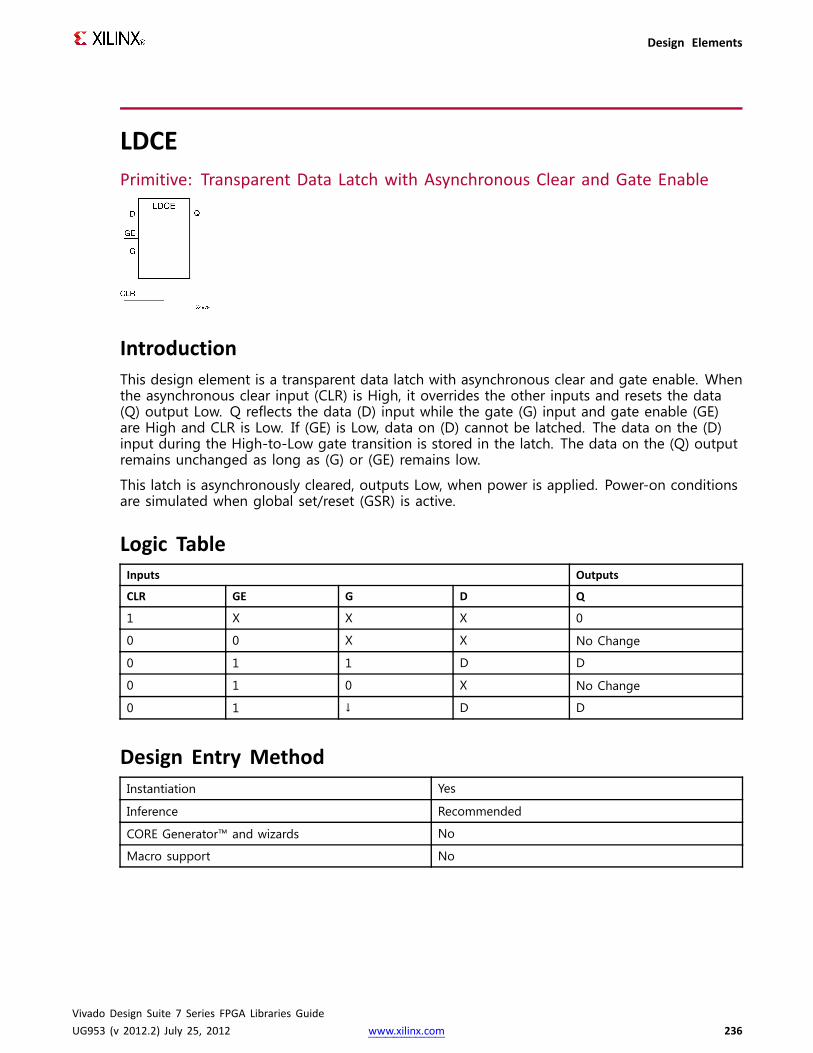
Design Elements
LDCEPrimitive: Transparent Data Latch with Asynchronous Clear and Gate Enable
IntroductionThis design element is a transparent data latch with asynchronous clear and gate enable. Whenthe asynchronous clear input (CLR) is High, it overrides the other inputs and resets the data(Q) output Low. Q reflects the data (D) input while the gate (G) input and gate enable (GE)are High and CLR is Low. If (GE) is Low, data on (D) cannot be latched. The data on the (D)input during the High-to-Low gate transition is stored in the latch. The data on the (Q) outputremains unchanged as long as (G) or (GE) remains low.
This latch is asynchronously cleared, outputs Low, when power is applied. Power-on conditionsare simulated when global set/reset (GSR) is active.
Logic TableInputs Outputs
CLR GE G D Q
1 X X X 0
0 0 X X No Change
0 1 1 D D
0 1 0 X No Change
0 1 ↓ D D
Design Entry MethodInstantiation Yes
Inference Recommended
CORE Generator™ and wizards No
Macro support No
Vivado Design Suite 7 Series FPGA Libraries GuideUG953 (v 2012.2) July 25, 2012 www.xilinx.com 236

Design Elements
Available AttributesAttribute Data Type Allowed Values Default Description
INIT Binary 0, 1 0 Sets the initial value of Q output afterconfiguration.
VHDL Instantiation TemplateUnless they already exist, copy the following two statements and paste them before the entitydeclaration.Library UNISIM;use UNISIM.vcomponents.all;
-- LDCE: Transparent latch with Asynchronous Reset and-- Gate Enable.-- 7 Series-- Xilinx HDL Libraries Guide, version 2012.2
LDCE_inst : LDCEgeneric map (
INIT => '0') -- Initial value of latch ('0' or '1')port map (
Q => Q, -- Data outputCLR => CLR, -- Asynchronous clear/reset inputD => D, -- Data inputG => G, -- Gate inputGE => GE -- Gate enable input
);
-- End of LDCE_inst instantiation
Verilog Instantiation Template
// LDCE: Transparent latch with Asynchronous Reset and Gate Enable.// 7 Series// Xilinx HDL Libraries Guide, version 2012.2
LDCE #(.INIT(1'b0) // Initial value of latch (1'b0 or 1'b1)
) LDCE_inst (.Q(Q), // Data output.CLR(CLR), // Asynchronous clear/reset input.D(D), // Data input.G(G), // Gate input.GE(GE) // Gate enable input
);
// End of LDCE_inst instantiation
For More InformationSee the 7 series FPGA User Documentation (User Guides and Data Sheets).
Vivado Design Suite 7 Series FPGA Libraries GuideUG953 (v 2012.2) July 25, 2012 www.xilinx.com 237
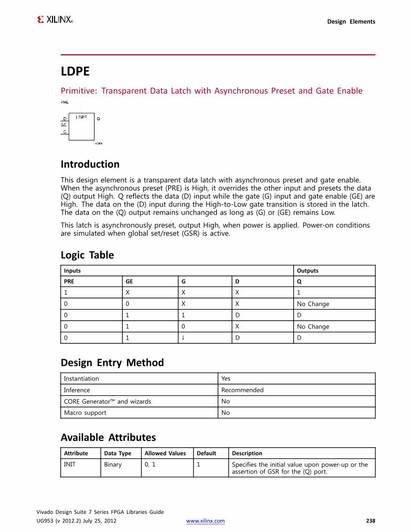
Design Elements
LDPEPrimitive: Transparent Data Latch with Asynchronous Preset and Gate Enable
IntroductionThis design element is a transparent data latch with asynchronous preset and gate enable.When the asynchronous preset (PRE) is High, it overrides the other input and presets the data(Q) output High. Q reflects the data (D) input while the gate (G) input and gate enable (GE) areHigh. The data on the (D) input during the High-to-Low gate transition is stored in the latch.The data on the (Q) output remains unchanged as long as (G) or (GE) remains Low.
This latch is asynchronously preset, output High, when power is applied. Power-on conditionsare simulated when global set/reset (GSR) is active.
Logic TableInputs Outputs
PRE GE G D Q
1 X X X 1
0 0 X X No Change
0 1 1 D D
0 1 0 X No Change
0 1 ↓ D D
Design Entry MethodInstantiation Yes
Inference Recommended
CORE Generator™ and wizards No
Macro support No
Available AttributesAttribute Data Type Allowed Values Default Description
INIT Binary 0, 1 1 Specifies the initial value upon power-up or theassertion of GSR for the (Q) port.
Vivado Design Suite 7 Series FPGA Libraries GuideUG953 (v 2012.2) July 25, 2012 www.xilinx.com 238

Design Elements
VHDL Instantiation TemplateUnless they already exist, copy the following two statements and paste them before the entitydeclaration.Library UNISIM;use UNISIM.vcomponents.all;
-- LDPE: Transparent latch with Asynchronous Set and-- Gate Enable.-- 7 Series-- Xilinx HDL Libraries Guide, version 2012.2
LDPE_inst : LDPEgeneric map (
INIT => '0') -- Initial value of latch ('0' or '1')port map (
Q => Q, -- Data outputCLR => CLR, -- Asynchronous preset/set inputD => D, -- Data inputG => G, -- Gate inputGE => GE -- Gate enable input
);
-- End of LDPE_inst instantiation
Verilog Instantiation Template
// LDPE: Transparent latch with Asynchronous Preset and Gate Enable.// 7 Series// Xilinx HDL Libraries Guide, version 2012.2
LDPE #(.INIT(1'b1) // Initial value of latch (1'b0 or 1'b1)
) LDPE_inst (.Q(Q), // Data output.PRE(PRE), // Asynchronous preset/set input.D(D), // Data input.G(G), // Gate input.GE(GE) // Gate enable input
);
// End of LDPE_inst instantiation
For More InformationSee the 7 series FPGA User Documentation (User Guides and Data Sheets).
Vivado Design Suite 7 Series FPGA Libraries GuideUG953 (v 2012.2) July 25, 2012 www.xilinx.com 239
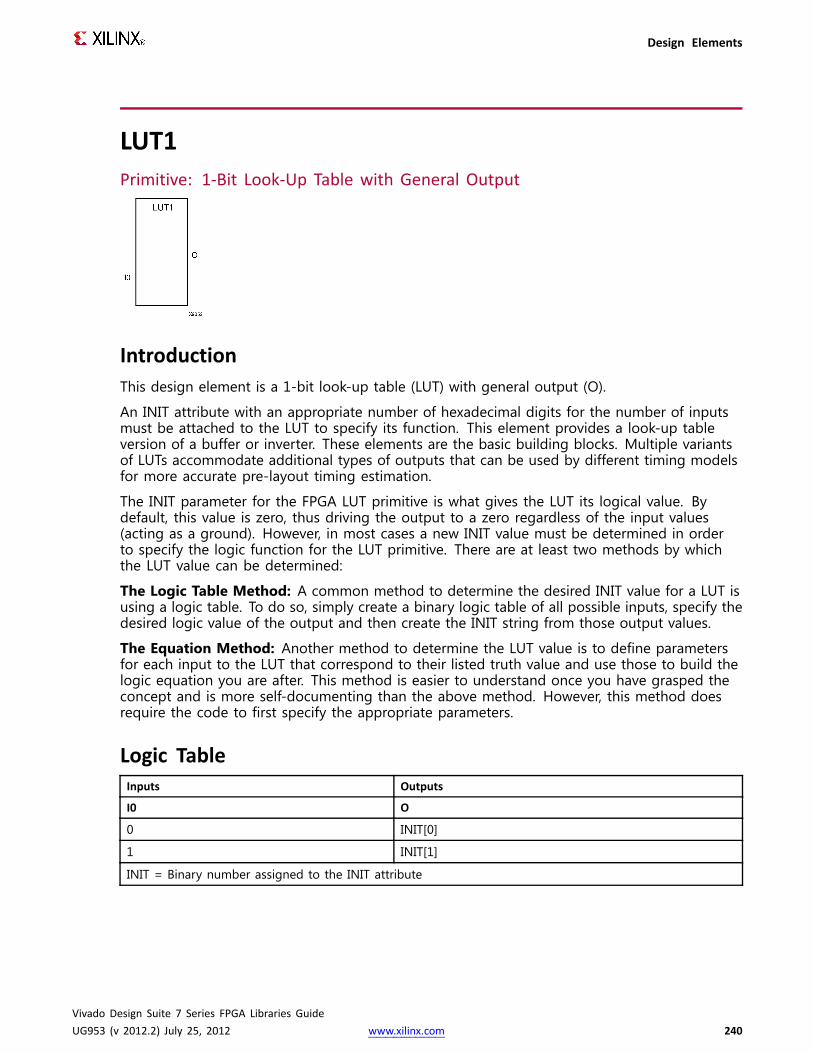
Design Elements
LUT1Primitive: 1-Bit Look-Up Table with General Output
IntroductionThis design element is a 1-bit look-up table (LUT) with general output (O).
An INIT attribute with an appropriate number of hexadecimal digits for the number of inputsmust be attached to the LUT to specify its function. This element provides a look-up tableversion of a buffer or inverter. These elements are the basic building blocks. Multiple variantsof LUTs accommodate additional types of outputs that can be used by different timing modelsfor more accurate pre-layout timing estimation.
The INIT parameter for the FPGA LUT primitive is what gives the LUT its logical value. Bydefault, this value is zero, thus driving the output to a zero regardless of the input values(acting as a ground). However, in most cases a new INIT value must be determined in orderto specify the logic function for the LUT primitive. There are at least two methods by whichthe LUT value can be determined:
The Logic Table Method: A common method to determine the desired INIT value for a LUT isusing a logic table. To do so, simply create a binary logic table of all possible inputs, specify thedesired logic value of the output and then create the INIT string from those output values.
The Equation Method: Another method to determine the LUT value is to define parametersfor each input to the LUT that correspond to their listed truth value and use those to build thelogic equation you are after. This method is easier to understand once you have grasped theconcept and is more self-documenting than the above method. However, this method doesrequire the code to first specify the appropriate parameters.
Logic TableInputs Outputs
I0 O
0 INIT[0]
1 INIT[1]
INIT = Binary number assigned to the INIT attribute
Vivado Design Suite 7 Series FPGA Libraries GuideUG953 (v 2012.2) July 25, 2012 www.xilinx.com 240

Design Elements
Design Entry MethodInstantiation Yes
Inference Recommended
CORE Generator™ and wizards No
Macro support No
Available AttributesAttribute Data Type Allowed Values Default Description
INIT Hexadecimal Any 2-Bit Value All zeros Initializes look-up tables.
VHDL Instantiation TemplateUnless they already exist, copy the following two statements and paste them before the entitydeclaration.Library UNISIM;use UNISIM.vcomponents.all;
-- LUT1: 1-input Look-Up Table with general output-- 7 Series-- Xilinx HDL Libraries Guide, version 2012.2
LUT1_inst : LUT1generic map (
INIT => "00")port map (
O => O, -- LUT general outputI0 => I0 -- LUT input
);
-- End of LUT1_inst instantiation
Verilog Instantiation Template
// LUT1: 1-input Look-Up Table with general output (Mapped to a LUT6)// 7 Series// Xilinx HDL Libraries Guide, version 2012.2
LUT1 #(.INIT(2'b00) // Specify LUT Contents
) LUT1_inst (.O(O), // LUT general output.I0(I0) // LUT input
);
// End of LUT1_inst instantiation
For More InformationSee the 7 series FPGA User Documentation (User Guides and Data Sheets).
Vivado Design Suite 7 Series FPGA Libraries GuideUG953 (v 2012.2) July 25, 2012 www.xilinx.com 241

Design Elements
LUT2Primitive: 2-Bit Look-Up Table with General Output
IntroductionThis design element is a 2-bit look-up table (LUT) with general output (O).
An INIT attribute with an appropriate number of hexadecimal digits for the number of inputsmust be attached to the LUT to specify its function. This element provides a look-up tableversion of a buffer or inverter. These elements are the basic building blocks. Multiple variantsof LUTs accommodate additional types of outputs that can be used by different timing modelsfor more accurate pre-layout timing estimation.
The INIT parameter for the FPGA LUT primitive is what gives the LUT its logical value. Bydefault, this value is zero, thus driving the output to a zero regardless of the input values(acting as a ground). However, in most cases a new INIT value must be determined in orderto specify the logic function for the LUT primitive. There are at least two methods by whichthe LUT value can be determined:
The Logic Table Method: A common method to determine the desired INIT value for a LUT isusing a logic table. To do so, simply create a binary logic table of all possible inputs, specify thedesired logic value of the output and then create the INIT string from those output values.
The Equation Method: Another method to determine the LUT value is to define parametersfor each input to the LUT that correspond to their listed truth value and use those to build thelogic equation you are after. This method is easier to understand once you have grasped theconcept and is more self-documenting than the above method. However, this method doesrequire the code to first specify the appropriate parameters.
Logic TableInputs Outputs
I1 I0 O
0 0 INIT[0]
0 1 INIT[1]
1 0 INIT[2]
1 1 INIT[3]
INIT = Binary equivalent of the hexadecimal number assigned to the INIT attribute
Vivado Design Suite 7 Series FPGA Libraries GuideUG953 (v 2012.2) July 25, 2012 www.xilinx.com 242
Design Elements
Design Entry MethodInstantiation Yes
Inference Recommended
CORE Generator™ and wizards No
Macro support No
Available AttributesAttribute Data Type Allowed Values Default Description
INIT Hexadecimal Any 4-Bit Value All zeros Initializes look-up tables.
VHDL Instantiation TemplateUnless they already exist, copy the following two statements and paste them before the entitydeclaration.Library UNISIM;use UNISIM.vcomponents.all;
-- LUT2: 2-input Look-Up Table with general output-- 7 Series-- Xilinx HDL Libraries Guide, version 2012.2
LUT2_inst : LUT2generic map (
INIT => X"0")port map (
O => O, -- LUT general outputI0 => I0, -- LUT inputI1 => I1 -- LUT input
);
-- End of LUT2_inst instantiation
Verilog Instantiation Template
// LUT2: 2-input Look-Up Table with general output (Mapped to a LUT6)// 7 Series// Xilinx HDL Libraries Guide, version 2012.2
LUT2 #(.INIT(4'h0) // Specify LUT Contents
) LUT2_inst (.O(O), // LUT general output.I0(I0), // LUT input.I1(I1) // LUT input
);
// End of LUT2_inst instantiation
For More InformationSee the 7 series FPGA User Documentation (User Guides and Data Sheets).
Vivado Design Suite 7 Series FPGA Libraries GuideUG953 (v 2012.2) July 25, 2012 www.xilinx.com 243
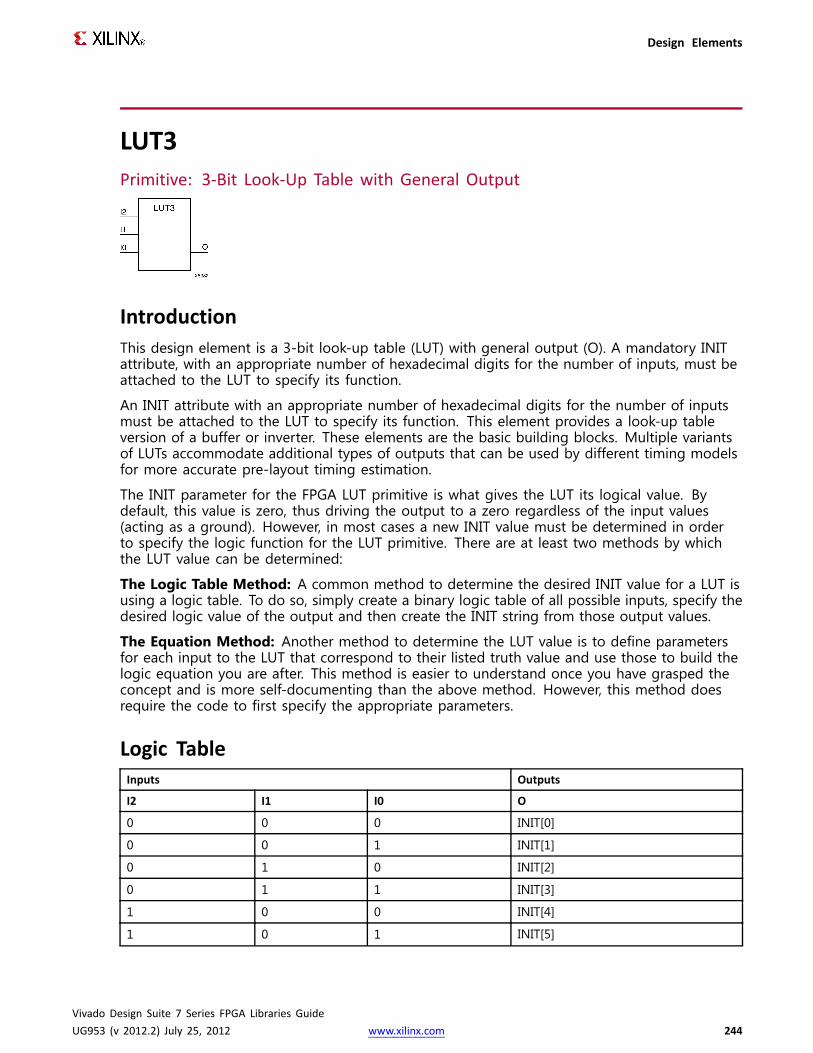
Design Elements
LUT3Primitive: 3-Bit Look-Up Table with General Output
IntroductionThis design element is a 3-bit look-up table (LUT) with general output (O). A mandatory INITattribute, with an appropriate number of hexadecimal digits for the number of inputs, must beattached to the LUT to specify its function.
An INIT attribute with an appropriate number of hexadecimal digits for the number of inputsmust be attached to the LUT to specify its function. This element provides a look-up tableversion of a buffer or inverter. These elements are the basic building blocks. Multiple variantsof LUTs accommodate additional types of outputs that can be used by different timing modelsfor more accurate pre-layout timing estimation.
The INIT parameter for the FPGA LUT primitive is what gives the LUT its logical value. Bydefault, this value is zero, thus driving the output to a zero regardless of the input values(acting as a ground). However, in most cases a new INIT value must be determined in orderto specify the logic function for the LUT primitive. There are at least two methods by whichthe LUT value can be determined:
The Logic Table Method: A common method to determine the desired INIT value for a LUT isusing a logic table. To do so, simply create a binary logic table of all possible inputs, specify thedesired logic value of the output and then create the INIT string from those output values.
The Equation Method: Another method to determine the LUT value is to define parametersfor each input to the LUT that correspond to their listed truth value and use those to build thelogic equation you are after. This method is easier to understand once you have grasped theconcept and is more self-documenting than the above method. However, this method doesrequire the code to first specify the appropriate parameters.
Logic TableInputs Outputs
I2 I1 I0 O
0 0 0 INIT[0]
0 0 1 INIT[1]
0 1 0 INIT[2]
0 1 1 INIT[3]
1 0 0 INIT[4]
1 0 1 INIT[5]
Vivado Design Suite 7 Series FPGA Libraries GuideUG953 (v 2012.2) July 25, 2012 www.xilinx.com 244

Design Elements
Inputs Outputs
I2 I1 I0 O
1 1 0 INIT[6]
1 1 1 INIT[7]
INIT = Binary equivalent of the hexadecimal number assigned to the INIT attribute
Design Entry MethodInstantiation Yes
Inference Recommended
CORE Generator™ and wizards No
Macro support No
Available AttributesAttribute Data Type Allowed Values Default Description
INIT Hexadecimal Any 8-Bit Value All zeros Initializes look-up tables.
VHDL Instantiation TemplateUnless they already exist, copy the following two statements and paste them before the entitydeclaration.Library UNISIM;use UNISIM.vcomponents.all;
-- LUT3: 3-input Look-Up Table with general output (Mapped to a LUT6)-- 7 Series-- Xilinx HDL Libraries Guide, version 2012.2
LUT3_inst : LUT3generic map (
INIT => X"00")port map (
O => O, -- LUT general outputI0 => I0, -- LUT inputI1 => I1, -- LUT inputI2 => I2 -- LUT input
);
-- End of LUT3_inst instantiation
Vivado Design Suite 7 Series FPGA Libraries GuideUG953 (v 2012.2) July 25, 2012 www.xilinx.com 245

Design Elements
Verilog Instantiation Template
// LUT3: 3-input Look-Up Table with general output (Mapped to a LUT6)// 7 Series// Xilinx HDL Libraries Guide, version 2012.2
LUT3 #(.INIT(8'h00) // Specify LUT Contents
) LUT3_inst (.O(O), // LUT general output.I0(I0), // LUT input.I1(I1), // LUT input.I2(I2) // LUT input
);
// End of LUT3_inst instantiation
For More InformationSee the 7 series FPGA User Documentation (User Guides and Data Sheets).
Vivado Design Suite 7 Series FPGA Libraries GuideUG953 (v 2012.2) July 25, 2012 www.xilinx.com 246

Design Elements
LUT4Primitive: 4-Bit Look-Up-Table with General Output
IntroductionThis design element is a 4-bit look-up table (LUT) with general output (O).
An INIT attribute with an appropriate number of hexadecimal digits for the number of inputsmust be attached to the LUT to specify its function. This element provides a look-up tableversion of a buffer or inverter. These elements are the basic building blocks. Multiple variantsof LUTs accommodate additional types of outputs that can be used by different timing modelsfor more accurate pre-layout timing estimation.
The INIT parameter for the FPGA LUT primitive is what gives the LUT its logical value. Bydefault, this value is zero, thus driving the output to a zero regardless of the input values(acting as a ground). However, in most cases a new INIT value must be determined in orderto specify the logic function for the LUT primitive. There are at least two methods by whichthe LUT value can be determined:
The Logic Table Method: A common method to determine the desired INIT value for a LUT isusing a logic table. To do so, simply create a binary logic table of all possible inputs, specify thedesired logic value of the output and then create the INIT string from those output values.
The Equation Method: Another method to determine the LUT value is to define parametersfor each input to the LUT that correspond to their listed truth value and use those to build thelogic equation you are after. This method is easier to understand once you have grasped theconcept and is more self-documenting than the above method. However, this method doesrequire the code to first specify the appropriate parameters.
Logic TableInputs Outputs
I3 I2 I1 I0 O
0 0 0 0 INIT[0]
0 0 0 1 INIT[1]
0 0 1 0 INIT[2]
0 0 1 1 INIT[3]
0 1 0 0 INIT[4]
0 1 0 1 INIT[5]
0 1 1 0 INIT[6]
Vivado Design Suite 7 Series FPGA Libraries GuideUG953 (v 2012.2) July 25, 2012 www.xilinx.com 247
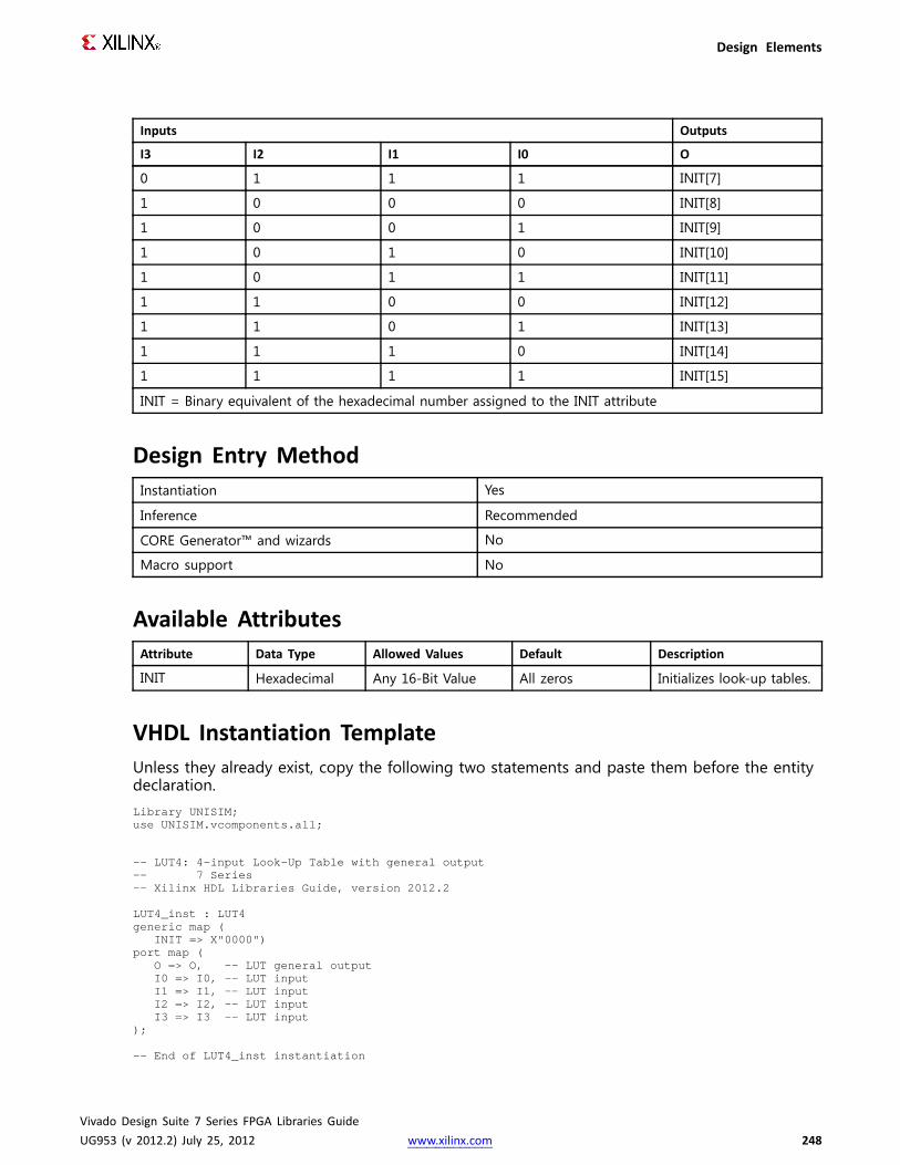
Design Elements
Inputs Outputs
I3 I2 I1 I0 O
0 1 1 1 INIT[7]
1 0 0 0 INIT[8]
1 0 0 1 INIT[9]
1 0 1 0 INIT[10]
1 0 1 1 INIT[11]
1 1 0 0 INIT[12]
1 1 0 1 INIT[13]
1 1 1 0 INIT[14]
1 1 1 1 INIT[15]
INIT = Binary equivalent of the hexadecimal number assigned to the INIT attribute
Design Entry MethodInstantiation Yes
Inference Recommended
CORE Generator™ and wizards No
Macro support No
Available AttributesAttribute Data Type Allowed Values Default Description
INIT Hexadecimal Any 16-Bit Value All zeros Initializes look-up tables.
VHDL Instantiation TemplateUnless they already exist, copy the following two statements and paste them before the entitydeclaration.Library UNISIM;use UNISIM.vcomponents.all;
-- LUT4: 4-input Look-Up Table with general output-- 7 Series-- Xilinx HDL Libraries Guide, version 2012.2
LUT4_inst : LUT4generic map (
INIT => X"0000")port map (
O => O, -- LUT general outputI0 => I0, -- LUT inputI1 => I1, -- LUT inputI2 => I2, -- LUT inputI3 => I3 -- LUT input
);
-- End of LUT4_inst instantiation
Vivado Design Suite 7 Series FPGA Libraries GuideUG953 (v 2012.2) July 25, 2012 www.xilinx.com 248

Design Elements
Verilog Instantiation Template
// LUT4: 4-input Look-Up Table with general output (Mapped to a LUT6)// 7 Series// Xilinx HDL Libraries Guide, version 2012.2
LUT4 #(.INIT(16'h0000) // Specify LUT Contents
) LUT4_inst (.O(O), // LUT general output.I0(I0), // LUT input.I1(I1), // LUT input.I2(I2), // LUT input.I3(I3) // LUT input
);
// End of LUT4_inst instantiation
For More InformationSee the 7 series FPGA User Documentation (User Guides and Data Sheets).
Vivado Design Suite 7 Series FPGA Libraries GuideUG953 (v 2012.2) July 25, 2012 www.xilinx.com 249

Design Elements
LUT5Primitive: 5-Input Lookup Table with General Output
IntroductionThis design element is a 5-input, 1-output look-up table (LUT) that can either act as anasynchronous 32-bit ROM (with 5-bit addressing) or implement any 5-input logic function. LUTsare the basic logic building blocks and are used to implement most logic functions of thedesign. One LUT5 is packed into a LUT6 within a slice, or two LUT5s can be packed into a singleLUT6 with some restrictions. The functionality of the LUT5, LUT5_L and LUT5_D is the same.However, the LUT5_L and LUT5_D allow the additional specification to connect the LUT5 outputsignal to an internal slice or CLB connection using the LO output. The LUT5_L specifies thatthe only connections from the LUT5 will be within a slice or CLB, while the LUT5_D allows thespecification to connect the output of the LUT to both inter-slice/CLB logic and external logic aswell. The LUT5 does not state any specific output connections and should be used in all casesexcept where internal slice or CLB signal connections must be implicitly specified.
An INIT attribute consisting of a 32-bit hexadecimal value must be specified to indicate theLUTs logical function. The INIT value is calculated by assigning a 1 to the correspondingINIT bit value when the associated inputs are applied. For instance, a Verilog INIT value of32'h80000000 (X"80000000" for VHDL) makes the output zero unless all of the inputs are one (a5-input AND gate). A Verilog INIT value of 32'hfffffffe (X"FFFFFFFE" for VHDL) makes the outputone unless all zeros are on the inputs (a 5-input OR gate).
The INIT parameter for the FPGA LUT primitive is what gives the LUT its logical value. Bydefault, this value is zero, thus driving the output to a zero regardless of the input values(acting as a ground). However, in most cases a new INIT value must be determined in orderto specify the logic function for the LUT primitive. There are at least two methods by whichthe LUT value can be determined:
The Logic Table Method: A common method to determine the desired INIT value for a LUT isusing a logic table. To do so, simply create a binary logic table of all possible inputs, specify thedesired logic value of the output and then create the INIT string from those output values.
The Equation Method: Another method to determine the LUT value is to define parametersfor each input to the LUT that correspond to their listed truth value and use those to build thelogic equation you are after. This method is easier to understand once you have grasped theconcept and is more self-documenting than the above method. However, this method doesrequire the code to first specify the appropriate parameters.
Vivado Design Suite 7 Series FPGA Libraries GuideUG953 (v 2012.2) July 25, 2012 www.xilinx.com 250

Design Elements
Logic TableInputs Outputs
I4 I3 I2 I1 I0 LO
0 0 0 0 0 INIT[0]
0 0 0 0 1 INIT[1]
0 0 0 1 0 INIT[2]
0 0 0 1 1 INIT[3]
0 0 1 0 0 INIT[4]
0 0 1 0 1 INIT[5]
0 0 1 1 0 INIT[6]
0 0 1 1 1 INIT[7]
0 1 0 0 0 INIT[8]
0 1 0 0 1 INIT[9]
0 1 0 1 0 INIT[10]
0 1 0 1 1 INIT[11]
0 1 1 0 0 INIT[12]
0 1 1 0 1 INIT[13]
0 1 1 1 0 INIT[14]
0 1 1 1 1 INIT[15]
1 0 0 0 0 INIT[16]
1 0 0 0 1 INIT[17]
1 0 0 1 0 INIT[18]
1 0 0 1 1 INIT[19]
1 0 1 0 0 INIT[20]
1 0 1 0 1 INIT[21]
1 0 1 1 0 INIT[22]
1 0 1 1 1 INIT[23]
1 1 0 0 0 INIT[24]
1 1 0 0 1 INIT[25]
1 1 0 1 0 INIT[26]
1 1 0 1 1 INIT[27]
1 1 1 0 0 INIT[28]
1 1 1 0 1 INIT[29]
1 1 1 1 0 INIT[30]
1 1 1 1 1 INIT[31]
INIT = Binary equivalent of the hexadecimal number assigned to the INIT attribute
Vivado Design Suite 7 Series FPGA Libraries GuideUG953 (v 2012.2) July 25, 2012 www.xilinx.com 251
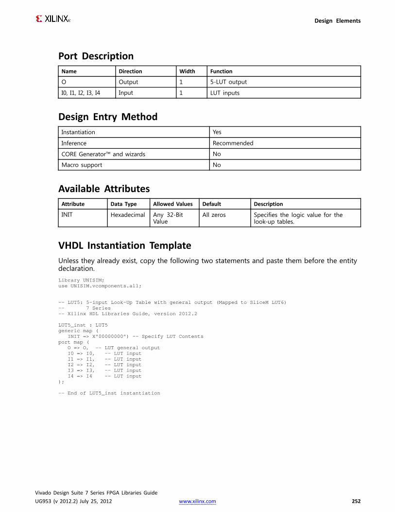
Design Elements
Port DescriptionName Direction Width Function
O Output 1 5-LUT output
I0, I1, I2, I3, I4 Input 1 LUT inputs
Design Entry MethodInstantiation Yes
Inference Recommended
CORE Generator™ and wizards No
Macro support No
Available AttributesAttribute Data Type Allowed Values Default Description
INIT Hexadecimal Any 32-BitValue
All zeros Specifies the logic value for thelook-up tables.
VHDL Instantiation TemplateUnless they already exist, copy the following two statements and paste them before the entitydeclaration.Library UNISIM;use UNISIM.vcomponents.all;
-- LUT5: 5-input Look-Up Table with general output (Mapped to SliceM LUT6)-- 7 Series-- Xilinx HDL Libraries Guide, version 2012.2
LUT5_inst : LUT5generic map (
INIT => X"00000000") -- Specify LUT Contentsport map (
O => O, -- LUT general outputI0 => I0, -- LUT inputI1 => I1, -- LUT inputI2 => I2, -- LUT inputI3 => I3, -- LUT inputI4 => I4 -- LUT input
);
-- End of LUT5_inst instantiation
Vivado Design Suite 7 Series FPGA Libraries GuideUG953 (v 2012.2) July 25, 2012 www.xilinx.com 252

Design Elements
Verilog Instantiation Template
// LUT5: 5-input Look-Up Table with general output (Mapped to a LUT6)// 7 Series// Xilinx HDL Libraries Guide, version 2012.2
LUT5 #(.INIT(32'h00000000) // Specify LUT Contents
) LUT5_inst (.O(O), // LUT general output.I0(I0), // LUT input.I1(I1), // LUT input.I2(I2), // LUT input.I3(I3), // LUT input.I4(I4) // LUT input
);
// End of LUT5_inst instantiation
For More InformationSee the 7 series FPGA User Documentation (User Guides and Data Sheets).
Vivado Design Suite 7 Series FPGA Libraries GuideUG953 (v 2012.2) July 25, 2012 www.xilinx.com 253
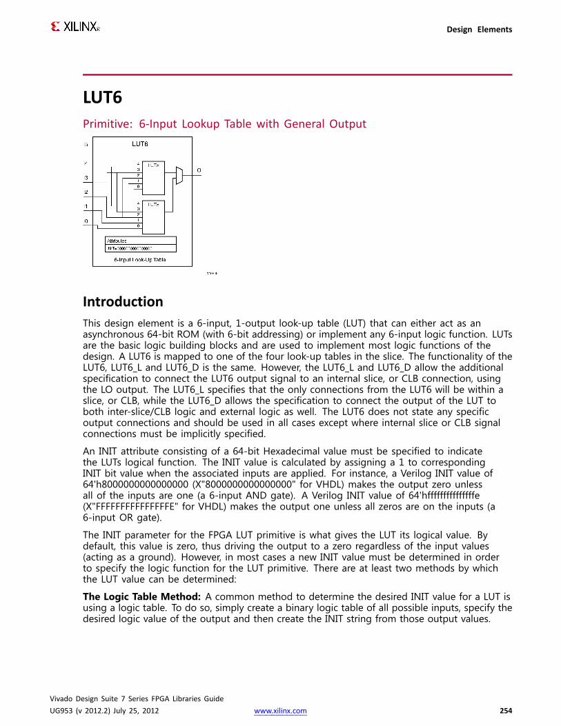
Design Elements
LUT6Primitive: 6-Input Lookup Table with General Output
IntroductionThis design element is a 6-input, 1-output look-up table (LUT) that can either act as anasynchronous 64-bit ROM (with 6-bit addressing) or implement any 6-input logic function. LUTsare the basic logic building blocks and are used to implement most logic functions of thedesign. A LUT6 is mapped to one of the four look-up tables in the slice. The functionality of theLUT6, LUT6_L and LUT6_D is the same. However, the LUT6_L and LUT6_D allow the additionalspecification to connect the LUT6 output signal to an internal slice, or CLB connection, usingthe LO output. The LUT6_L specifies that the only connections from the LUT6 will be within aslice, or CLB, while the LUT6_D allows the specification to connect the output of the LUT toboth inter-slice/CLB logic and external logic as well. The LUT6 does not state any specificoutput connections and should be used in all cases except where internal slice or CLB signalconnections must be implicitly specified.
An INIT attribute consisting of a 64-bit Hexadecimal value must be specified to indicatethe LUTs logical function. The INIT value is calculated by assigning a 1 to correspondingINIT bit value when the associated inputs are applied. For instance, a Verilog INIT value of64'h8000000000000000 (X"8000000000000000" for VHDL) makes the output zero unlessall of the inputs are one (a 6-input AND gate). A Verilog INIT value of 64'hfffffffffffffffe(X"FFFFFFFFFFFFFFFE" for VHDL) makes the output one unless all zeros are on the inputs (a6-input OR gate).
The INIT parameter for the FPGA LUT primitive is what gives the LUT its logical value. Bydefault, this value is zero, thus driving the output to a zero regardless of the input values(acting as a ground). However, in most cases a new INIT value must be determined in orderto specify the logic function for the LUT primitive. There are at least two methods by whichthe LUT value can be determined:
The Logic Table Method: A common method to determine the desired INIT value for a LUT isusing a logic table. To do so, simply create a binary logic table of all possible inputs, specify thedesired logic value of the output and then create the INIT string from those output values.
Vivado Design Suite 7 Series FPGA Libraries GuideUG953 (v 2012.2) July 25, 2012 www.xilinx.com 254

Design Elements
The Equation Method: Another method to determine the LUT value is to define parametersfor each input to the LUT that correspond to their listed truth value and use those to build thelogic equation you are after. This method is easier to understand once you have grasped theconcept and is more self-documenting than the above method. However, this method doesrequire the code to first specify the appropriate parameters.
Logic TableInputs Outputs
I5 I4 I3 I2 I1 I0 O
0 0 0 0 0 0 INIT[0]
0 0 0 0 0 1 INIT[1]
0 0 0 0 1 0 INIT[2]
0 0 0 0 1 1 INIT[3]
0 0 0 1 0 0 INIT[4]
0 0 0 1 0 1 INIT[5]
0 0 0 1 1 0 INIT[6]
0 0 0 1 1 1 INIT[7]
0 0 1 0 0 0 INIT[8]
0 0 1 0 0 1 INIT[9]
0 0 1 0 1 0 INIT[10]
0 0 1 0 1 1 INIT[11]
0 0 1 1 0 0 INIT[12]
0 0 1 1 0 1 INIT[13]
0 0 1 1 1 0 INIT[14]
0 0 1 1 1 1 INIT[15]
0 1 0 0 0 0 INIT[16]
0 1 0 0 0 1 INIT[17]
0 1 0 0 1 0 INIT[18]
0 1 0 0 1 1 INIT[19]
0 1 0 1 0 0 INIT[20]
0 1 0 1 0 1 INIT[21]
0 1 0 1 1 0 INIT[22]
0 1 0 1 1 1 INIT[23]
0 1 1 0 0 0 INIT[24]
0 1 1 0 0 1 INIT[25]
0 1 1 0 1 0 INIT[26]
0 1 1 0 1 1 INIT[27]
0 1 1 1 0 0 INIT[28]
0 1 1 1 0 1 INIT[29]
Vivado Design Suite 7 Series FPGA Libraries GuideUG953 (v 2012.2) July 25, 2012 www.xilinx.com 255

Design Elements
Inputs Outputs
I5 I4 I3 I2 I1 I0 O
0 1 1 1 1 0 INIT[30]
0 1 1 1 1 1 INIT[31]
1 0 0 0 0 0 INIT[32]
1 0 0 0 0 1 INIT[33]
1 0 0 0 1 0 INIT[34]
1 0 0 0 1 1 INIT[35]
1 0 0 1 0 0 INIT[36]
1 0 0 1 0 1 INIT[37]
1 0 0 1 1 0 INIT[38]
1 0 0 1 1 1 INIT[39]
1 0 1 0 0 0 INIT[40]
1 0 1 0 0 1 INIT[41]
1 0 1 0 1 0 INIT[42]
1 0 1 0 1 1 INIT[43]
1 0 1 1 0 0 INIT[44]
1 0 1 1 0 1 INIT[45]
1 0 1 1 1 0 INIT[46]
1 0 1 1 1 1 INIT[47]
1 1 0 0 0 0 INIT[48]
1 1 0 0 0 1 INIT[49]
1 1 0 0 1 0 INIT[50]
1 1 0 0 1 1 INIT[51]
1 1 0 1 0 0 INIT[52]
1 1 0 1 0 1 INIT[53]
1 1 0 1 1 0 INIT[54]
1 1 0 1 1 1 INIT[55]
1 1 1 0 0 0 INIT[56]
1 1 1 0 0 1 INIT[57]
1 1 1 0 1 0 INIT[58]
1 1 1 0 1 1 INIT[59]
1 1 1 1 0 0 INIT[60]
1 1 1 1 0 1 INIT[61]
1 1 1 1 1 0 INIT[62]
1 1 1 1 1 1 INIT[63]
INIT = Binary equivalent of the hexadecimal number assigned to the INIT attribute
Vivado Design Suite 7 Series FPGA Libraries GuideUG953 (v 2012.2) July 25, 2012 www.xilinx.com 256
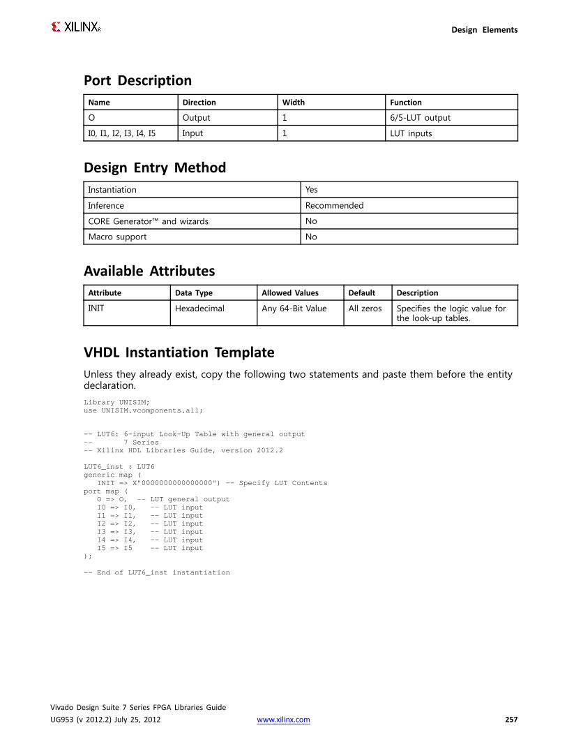
Design Elements
Port DescriptionName Direction Width Function
O Output 1 6/5-LUT output
I0, I1, I2, I3, I4, I5 Input 1 LUT inputs
Design Entry MethodInstantiation Yes
Inference Recommended
CORE Generator™ and wizards No
Macro support No
Available AttributesAttribute Data Type Allowed Values Default Description
INIT Hexadecimal Any 64-Bit Value All zeros Specifies the logic value forthe look-up tables.
VHDL Instantiation TemplateUnless they already exist, copy the following two statements and paste them before the entitydeclaration.Library UNISIM;use UNISIM.vcomponents.all;
-- LUT6: 6-input Look-Up Table with general output-- 7 Series-- Xilinx HDL Libraries Guide, version 2012.2
LUT6_inst : LUT6generic map (
INIT => X"0000000000000000") -- Specify LUT Contentsport map (
O => O, -- LUT general outputI0 => I0, -- LUT inputI1 => I1, -- LUT inputI2 => I2, -- LUT inputI3 => I3, -- LUT inputI4 => I4, -- LUT inputI5 => I5 -- LUT input
);
-- End of LUT6_inst instantiation
Vivado Design Suite 7 Series FPGA Libraries GuideUG953 (v 2012.2) July 25, 2012 www.xilinx.com 257
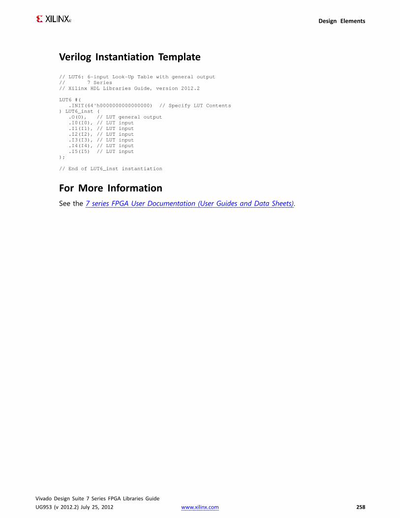
Design Elements
Verilog Instantiation Template
// LUT6: 6-input Look-Up Table with general output// 7 Series// Xilinx HDL Libraries Guide, version 2012.2
LUT6 #(.INIT(64'h0000000000000000) // Specify LUT Contents
) LUT6_inst (.O(O), // LUT general output.I0(I0), // LUT input.I1(I1), // LUT input.I2(I2), // LUT input.I3(I3), // LUT input.I4(I4), // LUT input.I5(I5) // LUT input
);
// End of LUT6_inst instantiation
For More InformationSee the 7 series FPGA User Documentation (User Guides and Data Sheets).
Vivado Design Suite 7 Series FPGA Libraries GuideUG953 (v 2012.2) July 25, 2012 www.xilinx.com 258

Design Elements
LUT6_2Primitive: Six-input, 2-output, Look-Up Table
IntroductionThis design element is a 6-input, 2-output look-up table (LUT) that can either act as a dualasynchronous 32-bit ROM (with 5-bit addressing), implement any two 5-input logic functionswith shared inputs, or implement a 6-input logic function and a 5-input logic function withshared inputs and shared logic values. LUTs are the basic logic building blocks and are used toimplement most logic functions of the design. A LUT6_2 will be mapped to one of the fourlook-up tables in the slice.
An INIT attribute consisting of a 64-bit hexadecimal value must be specified to indicate the LUTslogical function. The INIT value is calculated by assigning a 1 to corresponding INIT bit valuewhen the associated inputs are applied. For instance, a Verilog INIT value of 64'hfffffffffffffffe(X"FFFFFFFFFFFFFFFE" for VHDL) makes the O6 output 1 unless all zeros are on the inputs andthe O5 output a 1, or unless I[4:0] are all zeroes (a 5-input and 6-input OR gate). The lower half(bits 31:0) of the INIT values apply to the logic function of the O5 output.
The INIT parameter for the FPGA LUT primitive is what gives the LUT its logical value. Bydefault, this value is zero, thus driving the output to a zero regardless of the input values(acting as a ground). However, in most cases a new INIT value must be determined in orderto specify the logic function for the LUT primitive. There are at least two methods by whichthe LUT value can be determined:
The Logic Table Method: A common method to determine the desired INIT value for a LUT isusing a logic table. To do so, simply create a binary logic table of all possible inputs, specify thedesired logic value of the output and then create the INIT string from those output values.
The Equation Method: Another method to determine the LUT value is to define parametersfor each input to the LUT that correspond to their listed truth value and use those to build thelogic equation you are after. This method is easier to understand once you have grasped theconcept and is more self-documenting than the above method. However, this method doesrequire the code to first specify the appropriate parameters.
Vivado Design Suite 7 Series FPGA Libraries GuideUG953 (v 2012.2) July 25, 2012 www.xilinx.com 259
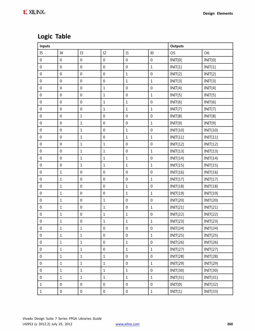
Design Elements
Logic TableInputs Outputs
I5 I4 I3 I2 I1 I0 O5 O6
0 0 0 0 0 0 INIT[0] INIT[0]
0 0 0 0 0 1 INIT[1] INIT[1]
0 0 0 0 1 0 INIT[2] INIT[2]
0 0 0 0 1 1 INIT[3] INIT[3]
0 0 0 1 0 0 INIT[4] INIT[4]
0 0 0 1 0 1 INIT[5] INIT[5]
0 0 0 1 1 0 INIT[6] INIT[6]
0 0 0 1 1 1 INIT[7] INIT[7]
0 0 1 0 0 0 INIT[8] INIT[8]
0 0 1 0 0 1 INIT[9] INIT[9]
0 0 1 0 1 0 INIT[10] INIT[10]
0 0 1 0 1 1 INIT[11] INIT[11]
0 0 1 1 0 0 INIT[12] INIT[12]
0 0 1 1 0 1 INIT[13] INIT[13]
0 0 1 1 1 0 INIT[14] INIT[14]
0 0 1 1 1 1 INIT[15] INIT[15]
0 1 0 0 0 0 INIT[16] INIT[16]
0 1 0 0 0 1 INIT[17] INIT[17]
0 1 0 0 1 0 INIT[18] INIT[18]
0 1 0 0 1 1 INIT[19] INIT[19]
0 1 0 1 0 0 INIT[20] INIT[20]
0 1 0 1 0 1 INIT[21] INIT[21]
0 1 0 1 1 0 INIT[22] INIT[22]
0 1 0 1 1 1 INIT[23] INIT[23]
0 1 1 0 0 0 INIT[24] INIT[24]
0 1 1 0 0 1 INIT[25] INIT[25]
0 1 1 0 1 0 INIT[26] INIT[26]
0 1 1 0 1 1 INIT[27] INIT[27]
0 1 1 1 0 0 INIT[28] INIT[28]
0 1 1 1 0 1 INIT[29] INIT[29]
0 1 1 1 1 0 INIT[30] INIT[30]
0 1 1 1 1 1 INIT[31] INIT[31]
1 0 0 0 0 0 INIT[0] INIT[32]
1 0 0 0 0 1 INIT[1] INIT[33]
Vivado Design Suite 7 Series FPGA Libraries GuideUG953 (v 2012.2) July 25, 2012 www.xilinx.com 260
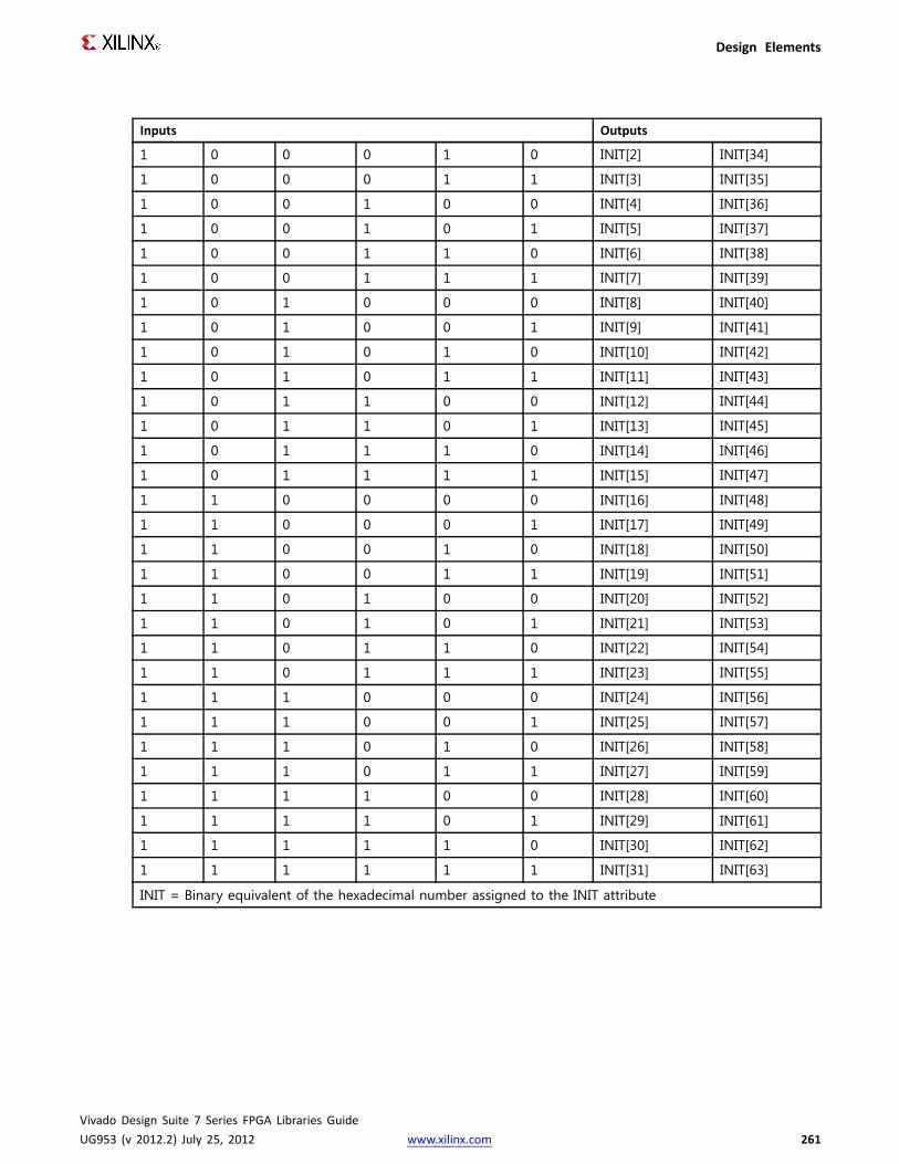
Design Elements
Inputs Outputs
1 0 0 0 1 0 INIT[2] INIT[34]
1 0 0 0 1 1 INIT[3] INIT[35]
1 0 0 1 0 0 INIT[4] INIT[36]
1 0 0 1 0 1 INIT[5] INIT[37]
1 0 0 1 1 0 INIT[6] INIT[38]
1 0 0 1 1 1 INIT[7] INIT[39]
1 0 1 0 0 0 INIT[8] INIT[40]
1 0 1 0 0 1 INIT[9] INIT[41]
1 0 1 0 1 0 INIT[10] INIT[42]
1 0 1 0 1 1 INIT[11] INIT[43]
1 0 1 1 0 0 INIT[12] INIT[44]
1 0 1 1 0 1 INIT[13] INIT[45]
1 0 1 1 1 0 INIT[14] INIT[46]
1 0 1 1 1 1 INIT[15] INIT[47]
1 1 0 0 0 0 INIT[16] INIT[48]
1 1 0 0 0 1 INIT[17] INIT[49]
1 1 0 0 1 0 INIT[18] INIT[50]
1 1 0 0 1 1 INIT[19] INIT[51]
1 1 0 1 0 0 INIT[20] INIT[52]
1 1 0 1 0 1 INIT[21] INIT[53]
1 1 0 1 1 0 INIT[22] INIT[54]
1 1 0 1 1 1 INIT[23] INIT[55]
1 1 1 0 0 0 INIT[24] INIT[56]
1 1 1 0 0 1 INIT[25] INIT[57]
1 1 1 0 1 0 INIT[26] INIT[58]
1 1 1 0 1 1 INIT[27] INIT[59]
1 1 1 1 0 0 INIT[28] INIT[60]
1 1 1 1 0 1 INIT[29] INIT[61]
1 1 1 1 1 0 INIT[30] INIT[62]
1 1 1 1 1 1 INIT[31] INIT[63]
INIT = Binary equivalent of the hexadecimal number assigned to the INIT attribute
Vivado Design Suite 7 Series FPGA Libraries GuideUG953 (v 2012.2) July 25, 2012 www.xilinx.com 261

Design Elements
Port DescriptionsPort Direction Width Function
O6 Output 1 6/5-LUT output
O5 Output 1 5-LUT output
I0, I1, I2, I3, I4, I5 Input 1 LUT inputs
Design Entry MethodInstantiation Yes
Inference Recommended
CORE Generator™ and wizards No
Macro support No
Available AttributesAttribute Data Type Allowed Values Default Description
INIT Hexadecimal Any 64-Bit Value All zeros Specifies the LUT5/6 outputfunction.
VHDL Instantiation TemplateUnless they already exist, copy the following two statements and paste them before the entitydeclaration.Library UNISIM;use UNISIM.vcomponents.all;
-- LUT6_2: 6-input 2 output Look-Up Table-- 7 Series-- Xilinx HDL Libraries Guide, version 2012.2
LUT6_2_inst : LUT6_2generic map (
INIT => X"0000000000000000") -- Specify LUT Contentsport map (
O6 => O6, -- 6/5-LUT output (1-bit)O5 => O5, -- 5-LUT output (1-bit)I0 => I0, -- LUT input (1-bit)I1 => I1, -- LUT input (1-bit)I2 => I2, -- LUT input (1-bit)I3 => I3, -- LUT input (1-bit)I4 => I4, -- LUT input (1-bit)I5 => I5 -- LUT input (1-bit)
);
-- End of LUT6_2_inst instantiation
Vivado Design Suite 7 Series FPGA Libraries GuideUG953 (v 2012.2) July 25, 2012 www.xilinx.com 262

Design Elements
Verilog Instantiation Template
// LUT6_2: 6-input, 2 output Look-Up Table// 7 Series// Xilinx HDL Libraries Guide, version 2012.2
LUT6_2 #(.INIT(64'h0000000000000000) // Specify LUT Contents
) LUT6_2_inst (.O6(O6), // 1-bit LUT6 output.O5(O5), // 1-bit lower LUT5 output.I0(I0), // 1-bit LUT input.I1(I1), // 1-bit LUT input.I2(I2), // 1-bit LUT input.I3(I3), // 1-bit LUT input.I4(I4), // 1-bit LUT input.I5(I5) // 1-bit LUT input (fast MUX select only available to O6 output)
);
// End of LUT6_2_inst instantiation
For More InformationSee the 7 series FPGA User Documentation (User Guides and Data Sheets).
Vivado Design Suite 7 Series FPGA Libraries GuideUG953 (v 2012.2) July 25, 2012 www.xilinx.com 263

Design Elements
MMCME2_ADVPrimitive: Advanced Mixed Mode Clock Manager
IntroductionThe MMCME2 is a mixed signal block designed to support frequency synthesis, clock networkdeskew, and jitter reduction. The clock outputs can each have an individual divide, phaseshift and duty cycle based on the same VCO frequency. Additionally, the MMCME2 supportsdynamic phase shifting and fractional divides.
Port DescriptionsPort Type Width Function
CLKFBIN Input 1 Feedback clock pin to the MMCM
CLKFBOUT Output 1 Dedicated MMCM Feedback clock output
CLKFBOUTB Output 1 Inverted CLKFBOUT
CLKFBSTOPPED Output 1 Status pin indicating that the feedback clock has stopped.
CLKINSEL Input 1 Signal controls the state of the input MUX, High = CLKIN1,Low = CLKIN2.
CLKINSTOPPED Output 1 Status pin indicating that the input clock has stopped.
CLKIN1 Input 1 Primary clock input.
Vivado Design Suite 7 Series FPGA Libraries GuideUG953 (v 2012.2) July 25, 2012 www.xilinx.com 264

Design Elements
Port Type Width Function
CLKIN2 Input 1 Secondary clock input to dynamically switch the MMCMreference clock.
CLKOUT0 Output 1 CLKOUT0 output
CLKOUT0B Output 1 Inverted CLKOUT0 output
CLKOUT1 Output 1 CLKOUT1 output
CLKOUT1B Output 1 Inverted CLKOUT1 output
CLKOUT2 Output 1 CLKOUT2 output
CLKOUT2B Output 1 Inverted CLKOUT2 output
CLKOUT3 Output 1 CLKOUT3 output
CLKOUT3B Output 1 Inverted CLKOUT3 output
CLKOUT4 Output 1 CLKOUT4 output
CLKOUT5 Output 1 CLKOUT5 output
CLKOUT6 Output 1 CLKOUT6 output
DADDR<6:0> Input 7 The dynamic reconfiguration address (DADDR) inputbus provides a reconfiguration address for the dynamicreconfiguration. When not used, all bits must be assignedzeros.
DCLK Input 1 The DCLK signal is the reference clock for the dynamicreconfiguration port.
DEN Input 1 The dynamic reconfiguration enable (DEN) provides the enablecontrol signal to access the dynamic reconfiguration feature.When the dynamic reconfiguration feature is not used, DENmust be tied Low.
DI<15:0> Input 16 The dynamic reconfiguration data input (DI) bus providesreconfiguration data. When not used, all bits must be set tozero.
DO<15:0> Output 16 The dynamic reconfiguration output bus provides MMCM dataoutput when using dynamic reconfiguration.
DRDY Output 1 The dynamic reconfiguration ready output (DRDY) providesthe response to the DEN signal for the MMCMs dynamicreconfiguration feature.
DWE Input 1 The dynamic reconfiguration write enable (DWE) input pinprovides the write enable control signal to write the DI datainto the DADDR address. When not used, it must be tied Low.
LOCKED Output 1 An output from the MMCM that indicates when the MMCMhas achieved phase alignment within a predefined windowand frequency matching within a predefined PPM range. TheMMCM automatically locks after power on, no extra reset isrequired. LOCKED will be deasserted if the input clock stopsor the phase alignment is violated (e.g., input clock phaseshift). The MMCM automatically reacquires lock after LOCKEDis deasserted.
PSCLK Input 1 Phase shift clock.
PSDONE Output 1 Phase shift done.
PSEN Input 1 Phase shift enable
Vivado Design Suite 7 Series FPGA Libraries GuideUG953 (v 2012.2) July 25, 2012 www.xilinx.com 265

Design Elements
Port Type Width Function
PSINCDEC Input 1 Phase shift increment/decrement control.
PWRDWN Input 1 Powers down instantiated but unused MMCMs.
RST Input 1 Asynchronous reset signal. The MMCM will synchronouslyre-enable itself when this signal is released (i.e., MMCMre-enabled). A reset is required when the input clock conditionschange (e.g., frequency).
Design Entry MethodInstantiation Yes
Inference No
CORE Generator™ and wizards Recommended
Macro support No
Available AttributesAttribute Type Allowed Values Default Description
BANDWIDTH STRING "OPTIMIZED","HIGH", "LOW"
"OPTIMIZED" Specifies the MMCM programmingalgorithm affecting the jitter, phasemargin and other characteristics ofthe MMCM.
CLKFBOUT_MULT_F
3significantdigit FLOAT
2.000 to 64.000 5.000 Specifies the amount to multiplyall CLKOUT clock outputs if adifferent frequency is desired. Thisnumber, in combination with theassociated CLKOUT#_DIVIDE valueand DIVCLK_DIVIDE value, willdetermine the output frequency.
CLKFBOUT_PHASE
3significantdigit FLOAT
-360.000 to 360.000 0.000 Specifies the phase offset indegrees of the clock feedbackoutput. Shifting the feedbackclock results in a negative phaseshift of all output clocks to theMMCM.
CLKIN1_PERIOD,CLKIN2_PERIOD
FLOAT(nS) 0.000 to 100.000 0.000 Specifies the input period in nsto the MMCM CLKIN inputs.Resolution is down to the ps.For exmaple a value of 33.333would indicate a 30 MHz inputclock. This information ismandatory and must be supplied.CLKIN1_PERIOD relates to theinput period on the CLKIN1 inputwhile CLKIN2_PERIOD relates tothe input clock period on theCLKIN2 input.
Vivado Design Suite 7 Series FPGA Libraries GuideUG953 (v 2012.2) July 25, 2012 www.xilinx.com 266

Design Elements
Attribute Type Allowed Values Default Description
CLKOUT1_DIVIDE,CLKOUT2_DIVIDE,CLKOUT3_DIVIDE,CLKOUT4_DIVIDE,CLKOUT5_DIVIDE,CLKOUT6_DIVIDE
DECIMAL 1 to 128 1 Specifies the amount to divide theassociated CLKOUT clock outputif a different frequency is desired.This number in combinationwith the CLKFBOUT_MULT_Fand DIVCLK_DIVIDE values willdetermine the output frequency.
CLKOUT0_DIVIDE_F
3significantdigit FLOAT
1.000 to 128.000 1.000 Specifies the amount to divide theassociated CLKOUT clock outputif a different frequency is desired.This number in combinationwith the CLKFBOUT_MULT_Fand DIVCLK_DIVIDE values willdetermine the output frequency.
CLKOUT0_DUTY_CYCLE toCLKOUT6_DUTY_CYCLE
3significantdigit FLOAT
0.001 to 0.999 0.500 Specifies the Duty Cycle of theassociated CLKOUT clock output inpercentage (i.e., 0.50 will generatea 50% duty cycle).
CLKOUT0_PHASE toCLKOUT6_PHASE
3significantdigit FLOAT
-360.000 to 360.000 0.000 Specifies the phase offset indegrees of the clock feedbackoutput. Shifting the feedbackclock results in a negative phaseshift of all output clocks to theMMCM.
CLKOUT4_CASCADE
BOOLEAN FALSE, TRUE FALSE Cascades the output divider(counter) into the input of theCLKOUT4 divider for an outputclock divider that is greater than128.
COMPENSATION STRING "ZHOLD", "BUF_IN","EXTERNAL","INTERNAL"
"ZHOLD" Clock input compensation. Shouldbe set to ZHOLD. Defines how theMMCM feedback is configured.
• "ZHOLD" - MMCM isconfigured to provide anegative hold time at theI/O registers.
• "INTERNAL" - MMCMis using its own internalfeedback path so no delayis being compensated.
• "EXTERNAL" - a networkexternal to the FPGA isbeing compensated.
• "BUF_IN" - configurationdoes not match withthe other compensationmodes and no delay willbe compensated. Thisis the case if a clock
Vivado Design Suite 7 Series FPGA Libraries GuideUG953 (v 2012.2) July 25, 2012 www.xilinx.com 267

Design Elements
Attribute Type Allowed Values Default Description
input is driven by aBUFG/BUFH/BUFR/GT.
DIVCLK _DIVIDE DECIMAL 1 to 106 1 Specifies the division ratio for alloutput clocks with respect to theinput clock. Effectively divides theCLKIN going into the PFD.
REF_JITTER1,REF_JITTER2
3significantdigit FLOAT
0.000 to 0.999 0.010 Allows specification of theexpected jitter on the CLKIN inputsin order to better optimize MMCMperformance. A bandwidth settingof OPTIMIZED will attempt tochoose the best parameter forinput clocking when unknown. Ifknown, then the value providedshould be specified in terms of theUI percentage (the maximum peakto peak value) of the expected jitteron the input clock. REF_JITTER1relates to the input jitter onCLKIN1 while REF_JITTER2 relatesto the input jitter on CLKIN2.
SS_EN STRING "FALSE", "TRUE" "FALSE" Enables the spread spectrumfeature for the MMCM. Used inconjunction with SS_MODE andSS_MOD_PERIOD attributes.
SS_MOD_PERIOD
DECIMAL(nS) 4000 to 40000 10000 Specifies the spread spectrummodulation period (ns).
SS_MODE STRING "CENTER_HIGH","CENTER_LOW","DOWN_HIGH","DOWN_LOW"
"CENTER_HIGH" Controls the spread spectrumfrequency deviation and thespread type.
STARTUP_WAIT BOOLEAN FALSE, TRUE FALSE Delays configuration DONE signalfrom asserting until MMCM islocked.
CLKFBOUT_USE_FINE_PS toCLKOUT6_USE_FINE_PS
BOOLEAN FALSE, TRUE FALSE Counter variable fine phase shiftenable.
VHDL Instantiation TemplateUnless they already exist, copy the following two statements and paste them before the entitydeclaration.Library UNISIM;use UNISIM.vcomponents.all;
-- MMCME2_ADV:Advanced Mixed Mode Clock Manager-- 7 Series-- Xilinx HDL Libraries Guide, version 2012.2
MMCME2_ADV_inst : MMCME2_ADVgeneric map (
BANDWIDTH=> "OPTIMIZED", -- Jitter programming (OPTIMIZED, HIGH, LOW)
Vivado Design Suite 7 Series FPGA Libraries GuideUG953 (v 2012.2) July 25, 2012 www.xilinx.com 268
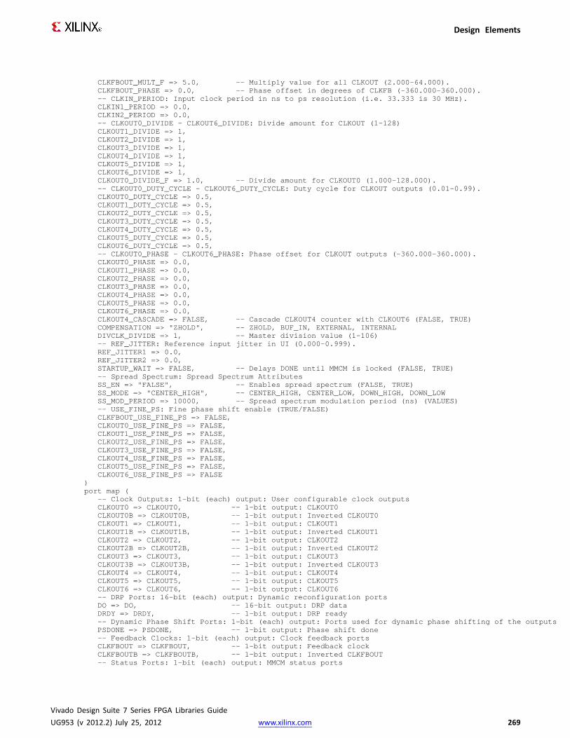
Design Elements
CLKFBOUT_MULT_F=> 5.0, -- Multiply value for all CLKOUT(2.000-64.000).CLKFBOUT_PHASE=> 0.0, -- Phase offset in degrees of CLKFB (-360.000-360.000).-- CLKIN_PERIOD: Input clock period in ns to ps resolution (i.e. 33.333 is 30 MHz).CLKIN1_PERIOD => 0.0,CLKIN2_PERIOD => 0.0,-- CLKOUT0_DIVIDE - CLKOUT6_DIVIDE: Divide amount for CLKOUT(1-128)CLKOUT1_DIVIDE => 1,CLKOUT2_DIVIDE => 1,CLKOUT3_DIVIDE => 1,CLKOUT4_DIVIDE => 1,CLKOUT5_DIVIDE => 1,CLKOUT6_DIVIDE => 1,CLKOUT0_DIVIDE_F => 1.0, -- Divide amount for CLKOUT0 (1.000-128.000).-- CLKOUT0_DUTY_CYCLE- CLKOUT6_DUTY_CYCLE:Duty cycle for CLKOUToutputs (0.01-0.99).CLKOUT0_DUTY_CYCLE=> 0.5,CLKOUT1_DUTY_CYCLE=> 0.5,CLKOUT2_DUTY_CYCLE=> 0.5,CLKOUT3_DUTY_CYCLE=> 0.5,CLKOUT4_DUTY_CYCLE=> 0.5,CLKOUT5_DUTY_CYCLE=> 0.5,CLKOUT6_DUTY_CYCLE=> 0.5,-- CLKOUT0_PHASE- CLKOUT6_PHASE:Phase offset for CLKOUToutputs (-360.000-360.000).CLKOUT0_PHASE=> 0.0,CLKOUT1_PHASE=> 0.0,CLKOUT2_PHASE=> 0.0,CLKOUT3_PHASE=> 0.0,CLKOUT4_PHASE=> 0.0,CLKOUT5_PHASE=> 0.0,CLKOUT6_PHASE=> 0.0,CLKOUT4_CASCADE=> FALSE, -- Cascade CLKOUT4 counter with CLKOUT6 (FALSE, TRUE)COMPENSATION=> "ZHOLD", -- ZHOLD, BUF_IN, EXTERNAL, INTERNALDIVCLK_DIVIDE => 1, -- Master division value (1-106)-- REF_JITTER: Reference input jitter in UI (0.000-0.999).REF_JITTER1 => 0.0,REF_JITTER2 => 0.0,STARTUP_WAIT=> FALSE, -- Delays DONEuntil MMCMis locked (FALSE, TRUE)-- Spread Spectrum: Spread Spectrum AttributesSS_EN => "FALSE", -- Enables spread spectrum (FALSE, TRUE)SS_MODE=> "CENTER_HIGH", -- CENTER_HIGH, CENTER_LOW,DOWN_HIGH,DOWN_LOWSS_MOD_PERIOD=> 10000, -- Spread spectrum modulation period (ns) (VALUES)-- USE_FINE_PS: Fine phase shift enable (TRUE/FALSE)CLKFBOUT_USE_FINE_PS=> FALSE,CLKOUT0_USE_FINE_PS=> FALSE,CLKOUT1_USE_FINE_PS=> FALSE,CLKOUT2_USE_FINE_PS=> FALSE,CLKOUT3_USE_FINE_PS=> FALSE,CLKOUT4_USE_FINE_PS=> FALSE,CLKOUT5_USE_FINE_PS=> FALSE,CLKOUT6_USE_FINE_PS=> FALSE
)port map (
-- Clock Outputs: 1-bit (each) output: User configurable clock outputsCLKOUT0 => CLKOUT0, -- 1-bit output: CLKOUT0CLKOUT0B=> CLKOUT0B, -- 1-bit output: Inverted CLKOUT0CLKOUT1 => CLKOUT1, -- 1-bit output: CLKOUT1CLKOUT1B=> CLKOUT1B, -- 1-bit output: Inverted CLKOUT1CLKOUT2 => CLKOUT2, -- 1-bit output: CLKOUT2CLKOUT2B=> CLKOUT2B, -- 1-bit output: Inverted CLKOUT2CLKOUT3 => CLKOUT3, -- 1-bit output: CLKOUT3CLKOUT3B=> CLKOUT3B, -- 1-bit output: Inverted CLKOUT3CLKOUT4 => CLKOUT4, -- 1-bit output: CLKOUT4CLKOUT5 => CLKOUT5, -- 1-bit output: CLKOUT5CLKOUT6 => CLKOUT6, -- 1-bit output: CLKOUT6-- DRP Ports: 16-bit (each) output: Dynamic reconfiguration portsDO => DO, -- 16-bit output: DRP dataDRDY=> DRDY, -- 1-bit output: DRP ready-- Dynamic Phase Shift Ports: 1-bit (each) output: Ports used for dynamic phase shifting of the outputsPSDONE=> PSDONE, -- 1-bit output: Phase shift done-- Feedback Clocks: 1-bit (each) output: Clock feedback portsCLKFBOUT=> CLKFBOUT, -- 1-bit output: Feedback clockCLKFBOUTB=> CLKFBOUTB, -- 1-bit output: Inverted CLKFBOUT-- Status Ports: 1-bit (each) output: MMCMstatus ports
Vivado Design Suite 7 Series FPGA Libraries GuideUG953 (v 2012.2) July 25, 2012 www.xilinx.com 269
Design Elements
CLKFBSTOPPED=> CLKFBSTOPPED,-- 1-bit output: Feedback clock stoppedCLKINSTOPPED=> CLKINSTOPPED, -- 1-bit output: Input clock stoppedLOCKED=> LOCKED, -- 1-bit output: LOCK-- Clock Inputs: 1-bit (each) input: Clock inputsCLKIN1 => CLKIN1, -- 1-bit input: Primary clockCLKIN2 => CLKIN2, -- 1-bit input: Secondary clock-- Control Ports: 1-bit (each) input: MMCMcontrol portsCLKINSEL => CLKINSEL, -- 1-bit input: Clock select, High=CLKIN1 Low=CLKIN2PWRDWN=> PWRDWN, -- 1-bit input: Power-downRST => RST, -- 1-bit input: Reset-- DRP Ports: 7-bit (each) input: Dynamic reconfiguration portsDADDR=> DADDR, -- 7-bit input: DRP addressDCLK => DCLK, -- 1-bit input: DRP clockDEN => DEN, -- 1-bit input: DRP enableDI => DI, -- 16-bit input: DRP dataDWE=> DWE, -- 1-bit input: DRP write enable-- Dynamic Phase Shift Ports: 1-bit (each) input: Ports used for dynamic phase shifting of the outputsPSCLK => PSCLK, -- 1-bit input: Phase shift clockPSEN => PSEN, -- 1-bit input: Phase shift enablePSINCDEC => PSINCDEC, -- 1-bit input: Phase shift increment/decrement-- Feedback Clocks: 1-bit (each) input: Clock feedback portsCLKFBIN => CLKFBIN -- 1-bit input: Feedback clock
);
-- End of MMCME2_ADV_inst instantiation
Verilog Instantiation Template
// MMCME2_ADV:Advanced Mixed Mode Clock Manager// 7 Series// Xilinx HDL Libraries Guide, version 2012.2
MMCME2_ADV#(.BANDWIDTH("OPTIMIZED"), // Jitter programming (OPTIMIZED, HIGH, LOW).CLKFBOUT_MULT_F(5.0), // Multiply value for all CLKOUT(2.000-64.000)..CLKFBOUT_PHASE(0.0), // Phase offset in degrees of CLKFB (-360.000-360.000).// CLKIN_PERIOD: Input clock period in ns to ps resolution (i.e. 33.333 is 30 MHz)..CLKIN1_PERIOD(0.0),.CLKIN2_PERIOD(0.0),// CLKOUT0_DIVIDE - CLKOUT6_DIVIDE: Divide amount for CLKOUT(1-128).CLKOUT1_DIVIDE(1),.CLKOUT2_DIVIDE(1),.CLKOUT3_DIVIDE(1),.CLKOUT4_DIVIDE(1),.CLKOUT5_DIVIDE(1),.CLKOUT6_DIVIDE(1),.CLKOUT0_DIVIDE_F(1.0), // Divide amount for CLKOUT0 (1.000-128.000).// CLKOUT0_DUTY_CYCLE- CLKOUT6_DUTY_CYCLE:Duty cycle for CLKOUToutputs (0.01-0.99)..CLKOUT0_DUTY_CYCLE(0.5),.CLKOUT1_DUTY_CYCLE(0.5),.CLKOUT2_DUTY_CYCLE(0.5),.CLKOUT3_DUTY_CYCLE(0.5),.CLKOUT4_DUTY_CYCLE(0.5),.CLKOUT5_DUTY_CYCLE(0.5),.CLKOUT6_DUTY_CYCLE(0.5),// CLKOUT0_PHASE- CLKOUT6_PHASE:Phase offset for CLKOUToutputs (-360.000-360.000)..CLKOUT0_PHASE(0.0),.CLKOUT1_PHASE(0.0),.CLKOUT2_PHASE(0.0),.CLKOUT3_PHASE(0.0),.CLKOUT4_PHASE(0.0),.CLKOUT5_PHASE(0.0),.CLKOUT6_PHASE(0.0),.CLKOUT4_CASCADE("FALSE"), // Cascade CLKOUT4 counter with CLKOUT6 (FALSE, TRUE).COMPENSATION("ZHOLD"), // ZHOLD, BUF_IN, EXTERNAL, INTERNAL.DIVCLK_DIVIDE(1), // Master division value (1-106)// REF_JITTER: Reference input jitter in UI (0.000-0.999)..REF_JITTER1(0.0),.REF_JITTER2(0.0),.STARTUP_WAIT("FALSE"), // Delays DONEuntil MMCMis locked (FALSE, TRUE)
Vivado Design Suite 7 Series FPGA Libraries GuideUG953 (v 2012.2) July 25, 2012 www.xilinx.com 270

Design Elements
// Spread Spectrum: Spread Spectrum Attributes.SS_EN("FALSE"), // Enables spread spectrum (FALSE, TRUE).SS_MODE("CENTER_HIGH"), // CENTER_HIGH, CENTER_LOW,DOWN_HIGH,DOWN_LOW.SS_MOD_PERIOD(10000), // Spread spectrum modulation period (ns) (VALUES)// USE_FINE_PS: Fine phase shift enable (TRUE/FALSE).CLKFBOUT_USE_FINE_PS("FALSE"),.CLKOUT0_USE_FINE_PS("FALSE"),.CLKOUT1_USE_FINE_PS("FALSE"),.CLKOUT2_USE_FINE_PS("FALSE"),.CLKOUT3_USE_FINE_PS("FALSE"),.CLKOUT4_USE_FINE_PS("FALSE"),.CLKOUT5_USE_FINE_PS("FALSE"),.CLKOUT6_USE_FINE_PS("FALSE")
)MMCME2_ADV_inst (
// Clock Outputs: 1-bit (each) output: User configurable clock outputs.CLKOUT0(CLKOUT0), // 1-bit output: CLKOUT0.CLKOUT0B(CLKOUT0B), // 1-bit output: Inverted CLKOUT0.CLKOUT1(CLKOUT1), // 1-bit output: CLKOUT1.CLKOUT1B(CLKOUT1B), // 1-bit output: Inverted CLKOUT1.CLKOUT2(CLKOUT2), // 1-bit output: CLKOUT2.CLKOUT2B(CLKOUT2B), // 1-bit output: Inverted CLKOUT2.CLKOUT3(CLKOUT3), // 1-bit output: CLKOUT3.CLKOUT3B(CLKOUT3B), // 1-bit output: Inverted CLKOUT3.CLKOUT4(CLKOUT4), // 1-bit output: CLKOUT4.CLKOUT5(CLKOUT5), // 1-bit output: CLKOUT5.CLKOUT6(CLKOUT6), // 1-bit output: CLKOUT6// DRP Ports: 16-bit (each) output: Dynamic reconfiguration ports.DO(DO), // 16-bit output: DRP data.DRDY(DRDY), // 1-bit output: DRP ready// Dynamic Phase Shift Ports: 1-bit (each) output: Ports used for dynamic phase shifting of the outputs.PSDONE(PSDONE), // 1-bit output: Phase shift done// Feedback Clocks: 1-bit (each) output: Clock feedback ports.CLKFBOUT(CLKFBOUT), // 1-bit output: Feedback clock.CLKFBOUTB(CLKFBOUTB), // 1-bit output: Inverted CLKFBOUT// Status Ports: 1-bit (each) output: MMCMstatus ports.CLKFBSTOPPED(CLKFBSTOPPED), // 1-bit output: Feedback clock stopped.CLKINSTOPPED(CLKINSTOPPED), // 1-bit output: Input clock stopped.LOCKED(LOCKED), // 1-bit output: LOCK// Clock Inputs: 1-bit (each) input: Clock inputs.CLKIN1(CLKIN1), // 1-bit input: Primary clock.CLKIN2(CLKIN2), // 1-bit input: Secondary clock// Control Ports: 1-bit (each) input: MMCMcontrol ports.CLKINSEL(CLKINSEL), // 1-bit input: Clock select, High=CLKIN1 Low=CLKIN2.PWRDWN(PWRDWN), // 1-bit input: Power-down.RST(RST), // 1-bit input: Reset// DRP Ports: 7-bit (each) input: Dynamic reconfiguration ports.DADDR(DADDR), // 7-bit input: DRP address.DCLK(DCLK), // 1-bit input: DRP clock.DEN(DEN), // 1-bit input: DRP enable.DI(DI), // 16-bit input: DRP data.DWE(DWE), // 1-bit input: DRP write enable// Dynamic Phase Shift Ports: 1-bit (each) input: Ports used for dynamic phase shifting of the outputs.PSCLK(PSCLK), // 1-bit input: Phase shift clock.PSEN(PSEN), // 1-bit input: Phase shift enable.PSINCDEC(PSINCDEC), // 1-bit input: Phase shift increment/decrement// Feedback Clocks: 1-bit (each) input: Clock feedback ports.CLKFBIN(CLKFBIN) // 1-bit input: Feedback clock
);
// End of MMCME2_ADV_inst instantiation
For More InformationSee the 7 series FPGA User Documentation (User Guides and Data Sheets).
Vivado Design Suite 7 Series FPGA Libraries GuideUG953 (v 2012.2) July 25, 2012 www.xilinx.com 271
Design Elements
MMCME2_BASEPrimitive: Base Mixed Mode Clock Manager
IntroductionThe MMCME2 is a mixed signal block designed to support frequency synthesis, clock networkdeskew, and jitter reduction. The clock outputs can each have an individual divide, phaseshift and duty cycle based on the same VCO frequency. Additionally, the MMCME2 supportsdynamic phase shifting and fractional divides.
Port DescriptionsPort Type Width Function
CLKFBIN Input 1 Feedback clock pin to the MMCM
CLKFBOUT Output 1 Dedicated MMCM Feedback clock output
CLKFBOUTB Output 1 Inverted CLKFBOUT output
CLKOUT0 Output 1 CLKOUT0 output
CLKOUT0B Output 1 Inverted CLKOUT0 output
CLKOUT1 Output 1 CLKOUT1 output
CLKOUT1B Output 1 Inverted CLKOUT1 output
Vivado Design Suite 7 Series FPGA Libraries GuideUG953 (v 2012.2) July 25, 2012 www.xilinx.com 272

Design Elements
Port Type Width Function
CLKOUT2 Output 1 CLKOUT2 output
CLKOUT2B Output 1 Inverted CLKOUT2 output
CLKOUT3 Output 1 CLKOUT3 output
CLKOUT3B Output 1 Inverted CLKOUT3 output
CLKOUT4 Output 1 CLKOUT4 output
CLKOUT5 Output 1 CLKOUT5 output
CLKOUT6 Output 1 CLKOUT6 output
Clock Inputs Input 1 General clock input.
PWRDWN Input 1 Powers down instantiated but unused MMCMs.
RST Input 1 Asynchronous reset signal. The MMCM will synchronouslyre-enable itself when this signal is released (i.e., MMCMre-enabled). A reset is required when the input clockconditions change (e.g., frequency).
Status Ports Output 1 An output from the MMCM that indicates when theMMCM has achieved phase alignment within a predefinedwindow and frequency matching within a predefined PPMrange. The MMCM automatically locks after power on,no extra reset is required. LOCKED will be deasserted ifthe input clock stops or the phase alignment is violated(e.g., input clock phase shift). The MMCM automaticallyreacquires lock after LOCKED is deasserted.
Design Entry MethodInstantiation Yes
Inference No
CORE Generator™ and wizards Recommended
Macro support No
Available AttributesAttribute Type Allowed Values Default Description
BANDWIDTH STRING "OPTIMIZED","HIGH", "LOW"
"OPTIMIZED" Specifies the MMCM programmingalgorithm affecting the jitter, phasemargin and other characteristics of theMMCM.
CLKFBOUT_MULT _F 3significantdigitFLOAT
2.000 to 64.000 5.000 Specifies the amount to multiplyall CLKOUT clock outputs if adifferent frequency is desired. Thisnumber, in combination with theassociated CLKOUT#_DIVIDE value andDIVCLK_DIVIDE value, will determinethe output frequency.
Vivado Design Suite 7 Series FPGA Libraries GuideUG953 (v 2012.2) July 25, 2012 www.xilinx.com 273
Design Elements
Attribute Type Allowed Values Default Description
CLKFBOUT _PHASE 3significantdigitFLOAT
-360.000 to360.000
0.000 Specifies the phase offset in degreesof the clock feedback output. Shiftingthe feedback clock results in a negativephase shift of all output clocks to theMMCM.
CLKIN1 _PERIOD FLOAT(nS) 0.000 to100.000
0.000 Specifies the input period in ns to theMMCM CLKIN1 input. Resolution isdown to the ps (3 decimal places).For example, a value of 33.333 wouldindicate a 30 MHz input clock. Thisinformation is mandatory and must besupplied.
CLKOUT1 _DIVIDE,CLKOUT2 _DIVIDE,CLKOUT3 _DIVIDE,CLKOUT4 _DIVIDE,CLKOUT5 _DIVIDE,CLKOUT6 _DIVIDE
DECIMAL 1 to 128 1 Specifies the amount to dividethe associated CLKOUT clockoutput if a different frequency isdesired. This number in combinationwith the CLKFBOUT_MULT_F andDIVCLK_DIVIDE values will determinethe output frequency.
CLKOUT0 _DIVIDE_F 3significantdigitFLOAT
1.000 to128.000
1.000 Specifies the amount to dividethe associated CLKOUT clockoutput if a different frequency isdesired. This number in combinationwith the CLKFBOUT_MULT_F andDIVCLK_DIVIDE values will determinethe output frequency.
CLKOUT0_DUTY_CYCLE toCLKOUT6_DUTY_CYCLE
3significantdigitFLOAT
0.001 to 0.999 0.500 Specifies the Duty Cycle of theassociated CLKOUT clock output inpercentage (i.e., 0.50 will generate a50% duty cycle).
CLKOUT0 _PHASE toCLKOUT6 _PHASE
3significantdigitFLOAT
-360.000 to360.000
0.000 Specifies the phase offset in degreesof the clock feedback output. Shiftingthe feedback clock results in a negativephase shift of all output clocks to theMMCM.
CLKOUT4 _CASCADE BOOLEAN FALSE, TRUE FALSE Cascades the output divider (counter)CLKOUT6 into the input of theCLKOUT4 divider for an output clockdivider that is greater than 128.
DIVCLK _DIVIDE DECIMAL 1 to 106 1 Specifies the division ratio for alloutput clocks with respect to the inputclock. Effectively divides the CLKINgoing into the PFD.
Vivado Design Suite 7 Series FPGA Libraries GuideUG953 (v 2012.2) July 25, 2012 www.xilinx.com 274

Design Elements
Attribute Type Allowed Values Default Description
REF_JITTER1 3significantdigitFLOAT
0.000 to 0.999 0.010 Allows specification of the expectedjitter on CLKIN1 in order to betteroptimize MMCM performance. Abandwidth setting of OPTIMIZED willattempt to choose the best parameterfor input clocking when unknown.If known, then the value providedshould be specified in terms of theUI percentage (the maximum peak topeak value) of the expected jitter onthe input clock.
STARTUP_WAIT BOOLEAN FALSE, TRUE FALSE Delays configuration DONE signal fromasserting until MMCM is locked.
VHDL Instantiation TemplateUnless they already exist, copy the following two statements and paste them before the entitydeclaration.Library UNISIM;use UNISIM.vcomponents.all;
-- MMCME2_BASE:Base Mixed Mode Clock Manager-- 7 Series-- Xilinx HDL Libraries Guide, version 2012.2
MMCME2_BASE_inst : MMCME2_BASEgeneric map (
BANDWIDTH=> "OPTIMIZED", -- Jitter programming (OPTIMIZED, HIGH, LOW)CLKFBOUT_MULT_F=> 5.0, -- Multiply value for all CLKOUT(2.000-64.000).CLKFBOUT_PHASE=> 0.0, -- Phase offset in degrees of CLKFB (-360.000-360.000).CLKIN1_PERIOD => 0.0, -- Input clock period in ns to ps resolution (i.e. 33.333 is 30 MHz).-- CLKOUT0_DIVIDE - CLKOUT6_DIVIDE: Divide amount for each CLKOUT(1-128)CLKOUT1_DIVIDE => 1,CLKOUT2_DIVIDE => 1,CLKOUT3_DIVIDE => 1,CLKOUT4_DIVIDE => 1,CLKOUT5_DIVIDE => 1,CLKOUT6_DIVIDE => 1,CLKOUT0_DIVIDE_F => 1.0, -- Divide amount for CLKOUT0 (1.000-128.000).-- CLKOUT0_DUTY_CYCLE- CLKOUT6_DUTY_CYCLE:Duty cycle for each CLKOUT(0.01-0.99).CLKOUT0_DUTY_CYCLE=> 0.5,CLKOUT1_DUTY_CYCLE=> 0.5,CLKOUT2_DUTY_CYCLE=> 0.5,CLKOUT3_DUTY_CYCLE=> 0.5,CLKOUT4_DUTY_CYCLE=> 0.5,CLKOUT5_DUTY_CYCLE=> 0.5,CLKOUT6_DUTY_CYCLE=> 0.5,-- CLKOUT0_PHASE- CLKOUT6_PHASE:Phase offset for each CLKOUT(-360.000-360.000).CLKOUT0_PHASE=> 0.0,CLKOUT1_PHASE=> 0.0,CLKOUT2_PHASE=> 0.0,CLKOUT3_PHASE=> 0.0,CLKOUT4_PHASE=> 0.0,CLKOUT5_PHASE=> 0.0,CLKOUT6_PHASE=> 0.0,CLKOUT4_CASCADE=> FALSE, -- Cascade CLKOUT4 counter with CLKOUT6 (FALSE, TRUE)DIVCLK_DIVIDE => 1, -- Master division value (1-106)REF_JITTER1 => 0.0, -- Reference input jitter in UI (0.000-0.999).STARTUP_WAIT=> FALSE -- Delays DONEuntil MMCMis locked (FALSE, TRUE)
)port map (
-- Clock Outputs: 1-bit (each) output: User configurable clock outputs
Vivado Design Suite 7 Series FPGA Libraries GuideUG953 (v 2012.2) July 25, 2012 www.xilinx.com 275

Design Elements
CLKOUT0 => CLKOUT0, -- 1-bit output: CLKOUT0CLKOUT0B=> CLKOUT0B, -- 1-bit output: Inverted CLKOUT0CLKOUT1 => CLKOUT1, -- 1-bit output: CLKOUT1CLKOUT1B=> CLKOUT1B, -- 1-bit output: Inverted CLKOUT1CLKOUT2 => CLKOUT2, -- 1-bit output: CLKOUT2CLKOUT2B=> CLKOUT2B, -- 1-bit output: Inverted CLKOUT2CLKOUT3 => CLKOUT3, -- 1-bit output: CLKOUT3CLKOUT3B=> CLKOUT3B, -- 1-bit output: Inverted CLKOUT3CLKOUT4 => CLKOUT4, -- 1-bit output: CLKOUT4CLKOUT5 => CLKOUT5, -- 1-bit output: CLKOUT5CLKOUT6 => CLKOUT6, -- 1-bit output: CLKOUT6-- Feedback Clocks: 1-bit (each) output: Clock feedback portsCLKFBOUT=> CLKFBOUT, -- 1-bit output: Feedback clockCLKFBOUTB=> CLKFBOUTB, -- 1-bit output: Inverted CLKFBOUT-- Status Ports: 1-bit (each) output: MMCMstatus portsLOCKED=> LOCKED, -- 1-bit output: LOCK-- Clock Inputs: 1-bit (each) input: Clock inputCLKIN1 => CLKIN1, -- 1-bit input: Clock-- Control Ports: 1-bit (each) input: MMCMcontrol portsPWRDWN=> PWRDWN, -- 1-bit input: Power-downRST => RST, -- 1-bit input: Reset-- Feedback Clocks: 1-bit (each) input: Clock feedback portsCLKFBIN => CLKFBIN -- 1-bit input: Feedback clock
);
-- End of MMCME2_BASE_inst instantiation
Vivado Design Suite 7 Series FPGA Libraries GuideUG953 (v 2012.2) July 25, 2012 www.xilinx.com 276

Design Elements
Verilog Instantiation Template
// MMCME2_BASE:Base Mixed Mode Clock Manager// 7 Series// Xilinx HDL Libraries Guide, version 2012.2
MMCME2_BASE#(.BANDWIDTH("OPTIMIZED"), // Jitter programming (OPTIMIZED, HIGH, LOW).CLKFBOUT_MULT_F(5.0), // Multiply value for all CLKOUT(2.000-64.000)..CLKFBOUT_PHASE(0.0), // Phase offset in degrees of CLKFB (-360.000-360.000)..CLKIN1_PERIOD(0.0), // Input clock period in ns to ps resolution (i.e. 33.333 is 30 MHz).// CLKOUT0_DIVIDE - CLKOUT6_DIVIDE: Divide amount for each CLKOUT(1-128).CLKOUT1_DIVIDE(1),.CLKOUT2_DIVIDE(1),.CLKOUT3_DIVIDE(1),.CLKOUT4_DIVIDE(1),.CLKOUT5_DIVIDE(1),.CLKOUT6_DIVIDE(1),.CLKOUT0_DIVIDE_F(1.0), // Divide amount for CLKOUT0 (1.000-128.000).// CLKOUT0_DUTY_CYCLE- CLKOUT6_DUTY_CYCLE:Duty cycle for each CLKOUT(0.01-0.99)..CLKOUT0_DUTY_CYCLE(0.5),.CLKOUT1_DUTY_CYCLE(0.5),.CLKOUT2_DUTY_CYCLE(0.5),.CLKOUT3_DUTY_CYCLE(0.5),.CLKOUT4_DUTY_CYCLE(0.5),.CLKOUT5_DUTY_CYCLE(0.5),.CLKOUT6_DUTY_CYCLE(0.5),// CLKOUT0_PHASE- CLKOUT6_PHASE:Phase offset for each CLKOUT(-360.000-360.000)..CLKOUT0_PHASE(0.0),.CLKOUT1_PHASE(0.0),.CLKOUT2_PHASE(0.0),.CLKOUT3_PHASE(0.0),.CLKOUT4_PHASE(0.0),.CLKOUT5_PHASE(0.0),.CLKOUT6_PHASE(0.0),.CLKOUT4_CASCADE("FALSE"), // Cascade CLKOUT4 counter with CLKOUT6 (FALSE, TRUE).DIVCLK_DIVIDE(1), // Master division value (1-106).REF_JITTER1(0.0), // Reference input jitter in UI (0.000-0.999)..STARTUP_WAIT("FALSE") // Delays DONEuntil MMCMis locked (FALSE, TRUE)
)MMCME2_BASE_inst (
// Clock Outputs: 1-bit (each) output: User configurable clock outputs.CLKOUT0(CLKOUT0), // 1-bit output: CLKOUT0.CLKOUT0B(CLKOUT0B), // 1-bit output: Inverted CLKOUT0.CLKOUT1(CLKOUT1), // 1-bit output: CLKOUT1.CLKOUT1B(CLKOUT1B), // 1-bit output: Inverted CLKOUT1.CLKOUT2(CLKOUT2), // 1-bit output: CLKOUT2.CLKOUT2B(CLKOUT2B), // 1-bit output: Inverted CLKOUT2.CLKOUT3(CLKOUT3), // 1-bit output: CLKOUT3.CLKOUT3B(CLKOUT3B), // 1-bit output: Inverted CLKOUT3.CLKOUT4(CLKOUT4), // 1-bit output: CLKOUT4.CLKOUT5(CLKOUT5), // 1-bit output: CLKOUT5.CLKOUT6(CLKOUT6), // 1-bit output: CLKOUT6// Feedback Clocks: 1-bit (each) output: Clock feedback ports.CLKFBOUT(CLKFBOUT), // 1-bit output: Feedback clock.CLKFBOUTB(CLKFBOUTB), // 1-bit output: Inverted CLKFBOUT// Status Ports: 1-bit (each) output: MMCMstatus ports.LOCKED(LOCKED), // 1-bit output: LOCK// Clock Inputs: 1-bit (each) input: Clock input.CLKIN1(CLKIN1), // 1-bit input: Clock// Control Ports: 1-bit (each) input: MMCMcontrol ports.PWRDWN(PWRDWN), // 1-bit input: Power-down.RST(RST), // 1-bit input: Reset// Feedback Clocks: 1-bit (each) input: Clock feedback ports.CLKFBIN(CLKFBIN) // 1-bit input: Feedback clock
);
// End of MMCME2_BASE_inst instantiation
Vivado Design Suite 7 Series FPGA Libraries GuideUG953 (v 2012.2) July 25, 2012 www.xilinx.com 277

Design Elements
For More InformationSee the 7 series FPGA User Documentation (User Guides and Data Sheets).
Vivado Design Suite 7 Series FPGA Libraries GuideUG953 (v 2012.2) July 25, 2012 www.xilinx.com 278
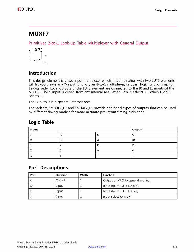
Design Elements
MUXF7Primitive: 2-to-1 Look-Up Table Multiplexer with General Output
IntroductionThis design element is a two input multiplexer which, in combination with two LUT6 elementswill let you create any 7-input function, an 8-to-1 multiplexer, or other logic functions up to12-bits wide. Local outputs of the LUT6 element are connected to the I0 and I1 inputs of theMUXF7. The S input is driven from any internal net. When Low, S selects I0. When High, Sselects I1.
The O output is a general interconnect.
The variants, "MUXF7_D" and "MUXF7_L", provide additional types of outputs that can be usedby different timing models for more accurate pre-layout timing estimation.
Logic TableInputs Outputs
S I0 I1 O
0 I0 X I0
1 X I1 I1
X 0 0 0
X 1 1 1
Port DescriptionsPort Direction Width Function
O Output 1 Output of MUX to general routing.
I0 Input 1 Input (tie to LUT6 LO out).
I1 Input 1 Input (tie to LUT6 LO out).
S Input 1 Input select to MUX.
Vivado Design Suite 7 Series FPGA Libraries GuideUG953 (v 2012.2) July 25, 2012 www.xilinx.com 279

Design Elements
Design Entry MethodInstantiation Yes
Inference Recommended
CORE Generator™ and wizards No
Macro support No
VHDL Instantiation TemplateUnless they already exist, copy the following two statements and paste them before the entitydeclaration.Library UNISIM;use UNISIM.vcomponents.all;
-- MUXF7: CLB MUX to tie two LUT6's together with general output-- 7 Series-- Xilinx HDL Libraries Guide, version 2012.2
MUXF7_inst : MUXF7port map (
O => O, -- Output of MUX to general routingI0 => I0, -- Input (tie to LUT6 O6 pin)I1 => I1, -- Input (tie to LUT6 O6 pin)S => S -- Input select to MUX
);
-- End of MUXF7_inst instantiation
Verilog Instantiation Template
// MUXF7: CLB MUX to tie two LUT6's together with general output// 7 Series// Xilinx HDL Libraries Guide, version 2012.2
MUXF7MUXF7_inst (.O(O), // Output of MUX to general routing.I0(I0), // Input (tie to LUT6 O6 pin).I1(I1), // Input (tie to LUT6 O6 pin).S(S) // Input select to MUX
);
// End of MUXF7_inst instantiation
For More InformationSee the 7 series FPGA User Documentation (User Guides and Data Sheets).
Vivado Design Suite 7 Series FPGA Libraries GuideUG953 (v 2012.2) July 25, 2012 www.xilinx.com 280
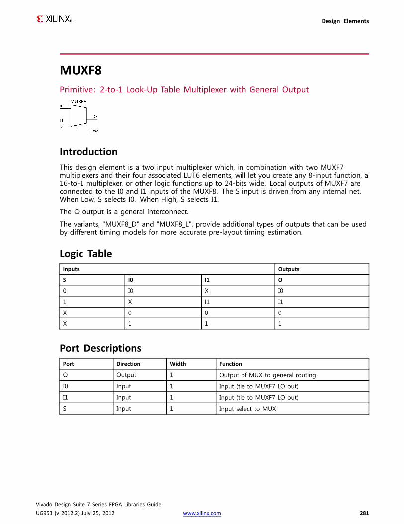
Design Elements
MUXF8Primitive: 2-to-1 Look-Up Table Multiplexer with General Output
IntroductionThis design element is a two input multiplexer which, in combination with two MUXF7multiplexers and their four associated LUT6 elements, will let you create any 8-input function, a16-to-1 multiplexer, or other logic functions up to 24-bits wide. Local outputs of MUXF7 areconnected to the I0 and I1 inputs of the MUXF8. The S input is driven from any internal net.When Low, S selects I0. When High, S selects I1.
The O output is a general interconnect.
The variants, "MUXF8_D" and "MUXF8_L", provide additional types of outputs that can be usedby different timing models for more accurate pre-layout timing estimation.
Logic TableInputs Outputs
S I0 I1 O
0 I0 X I0
1 X I1 I1
X 0 0 0
X 1 1 1
Port DescriptionsPort Direction Width Function
O Output 1 Output of MUX to general routing
I0 Input 1 Input (tie to MUXF7 LO out)
I1 Input 1 Input (tie to MUXF7 LO out)
S Input 1 Input select to MUX
Vivado Design Suite 7 Series FPGA Libraries GuideUG953 (v 2012.2) July 25, 2012 www.xilinx.com 281

Design Elements
Design Entry MethodInstantiation Yes
Inference Recommended
CORE Generator™ and wizards No
Macro support No
VHDL Instantiation TemplateUnless they already exist, copy the following two statements and paste them before the entitydeclaration.Library UNISIM;use UNISIM.vcomponents.all;
-- MUXF8: CLB MUX to tie two MUXF7's together with general output-- 7 Series-- Xilinx HDL Libraries Guide, version 2012.2
MUXF8_inst : MUXF8port map (
O => O, -- Output of MUX to general routingI0 => I0, -- Input (tie to MUXF7 L/LO out)I1 => I1, -- Input (tie to MUXF7 L/LO out)S => S -- Input select to MUX
);
-- End of MUXF8_inst instantiation
Verilog Instantiation Template
// MUXF8: CLB MUX to tie two MUXF7's together with general output// 7 Series// Xilinx HDL Libraries Guide, version 2012.2
MUXF8MUXF8_inst (.O(O), // Output of MUX to general routing.I0(I0), // Input (tie to MUXF7 L/LO out).I1(I1), // Input (tie to MUXF7 L/LO out).S(S) // Input select to MUX
);
// End of MUXF8_inst instantiation
For More InformationSee the 7 series FPGA User Documentation (User Guides and Data Sheets).
Vivado Design Suite 7 Series FPGA Libraries GuideUG953 (v 2012.2) July 25, 2012 www.xilinx.com 282

Design Elements
OBUFPrimitive: Output Buffer
IntroductionThis design element is a simple output buffer used to drive output signals to the FPGA devicepins that do not need to be 3-stated (constantly driven). Either an OBUF, OBUFT, OBUFDS, orOBUFTDS must be connected to every output port in the design.
This element isolates the internal circuit and provides drive current for signals leaving a chip. Itexists in input/output blocks (IOB). Its output (O) is connected to an OPAD or an IOPAD. Theinterface standard used by this element is LVCMOS18. Also, this element has selectable driveand slew rates using the DRIVE and SLOW or FAST constraints.
Port DescriptionsPort Direction Width Function
O Output 1 Output of OBUF to be connected directly to top-leveloutput port.
I Input 1 Input of OBUF. Connect to the logic driving theoutput port.
Design Entry MethodInstantiation Yes
Inference Recommended
CORE Generator™ and wizards No
Macro support No
Available Attributes
AttributeDataType Allowed Values Default Description
DRIVE Integer 2, 4, 6, 8, 12, 16,24
12 Specifies the output current drivestrength of the I/O. It is suggestedthat you set this to the lowest settingtolerable for the design drive and timingrequirements.
IOSTANDARD String See Data Sheet "DEFAULT" Assigns an I/O standard to the element.
Vivado Design Suite 7 Series FPGA Libraries GuideUG953 (v 2012.2) July 25, 2012 www.xilinx.com 283

Design Elements
AttributeDataType Allowed Values Default Description
SLEW String "SLOW" or "FAST" "SLOW" Specifies the slew rate of the outputdriver. Consult the product Data Sheetfor recommendations of the best settingfor this attribute.
VHDL Instantiation TemplateUnless they already exist, copy the following two statements and paste them before the entitydeclaration.Library UNISIM;use UNISIM.vcomponents.all;
-- OBUF: Single-ended Output Buffer-- 7 Series-- Xilinx HDL Libraries Guide, version 2012.2
OBUF_inst : OBUFgeneric map (
DRIVE => 12,IOSTANDARD=> "DEFAULT",SLEW=> "SLOW")
port map (O => O, -- Buffer output (connect directly to top-level port)I => I -- Buffer input
);
-- End of OBUF_inst instantiation
Verilog Instantiation Template
// OBUF: Single-ended Output Buffer// 7 Series// Xilinx HDL Libraries Guide, version 2012.2
OBUF #(.DRIVE(12), // Specify the output drive strength.IOSTANDARD("DEFAULT"), // Specify the output I/O standard.SLEW("SLOW") // Specify the output slew rate
) OBUF_inst (.O(O), // Buffer output (connect directly to top-level port).I(I) // Buffer input
);
// End of OBUF_inst instantiation
For More InformationSee the 7 series FPGA User Documentation (User Guides and Data Sheets).
Vivado Design Suite 7 Series FPGA Libraries GuideUG953 (v 2012.2) July 25, 2012 www.xilinx.com 284

Design Elements
OBUFDSPrimitive: Differential Signaling Output Buffer
IntroductionThis design element is a single output buffer that supports low-voltage, differential signaling.OBUFDS isolates the internal circuit and provides drive current for signals leaving the chip. Itsoutput is represented as two distinct ports (O and OB), one deemed the "master" and theother the "slave." The master and the slave are opposite phases of the same logical signal(for example, MYNET and MYNETB).
Logic TableInputs Outputs
I O OB
0 0 1
1 1 0
Port DescriptionsPort Direction Width Function
O Output 1 Diff_p output (connect directly to top level port)
OB Output 1 Diff_n output (connect directly to top level port)
I Input 1 Buffer input
Design Entry MethodInstantiation Recommended
Inference No
CORE Generator™ and wizards No
Macro support No
Vivado Design Suite 7 Series FPGA Libraries GuideUG953 (v 2012.2) July 25, 2012 www.xilinx.com 285
Design Elements
Available Attributes
AttributeDataType Allowed Values Default Description
IOSTANDARD String See DataSheet
"DEFAULT" Assigns an I/O standard to the element.
SLEW String "SLOW" or"FAST"
"SLOW" Specifies the slew rate of the outputdriver. Consult the product Data Sheetfor recommendations of the best settingfor this attribute.
VHDL Instantiation TemplateUnless they already exist, copy the following two statements and paste them before the entitydeclaration.Library UNISIM;use UNISIM.vcomponents.all;
-- OBUFDS: Differential Output Buffer-- 7 Series-- Xilinx HDL Libraries Guide, version 2012.2
OBUFDS_inst : OBUFDSgeneric map (
IOSTANDARD=> "DEFAULT", -- Specify the output I/O standardSLEW=> "SLOW") -- Specify the output slew rate
port map (O => O, -- Diff_p output (connect directly to top-level port)OB => OB, -- Diff_n output (connect directly to top-level port)I => I -- Buffer input
);
-- End of OBUFDS_inst instantiation
Verilog Instantiation Template
// OBUFDS: Differential Output Buffer// 7 Series// Xilinx HDL Libraries Guide, version 2012.2
OBUFDS#(.IOSTANDARD("DEFAULT"), // Specify the output I/O standard.SLEW("SLOW") // Specify the output slew rate
) OBUFDS_inst (.O(O), // Diff_p output (connect directly to top-level port).OB(OB), // Diff_n output (connect directly to top-level port).I(I) // Buffer input
);
// End of OBUFDS_inst instantiation
For More InformationSee the 7 series FPGA User Documentation (User Guides and Data Sheets).
Vivado Design Suite 7 Series FPGA Libraries GuideUG953 (v 2012.2) July 25, 2012 www.xilinx.com 286
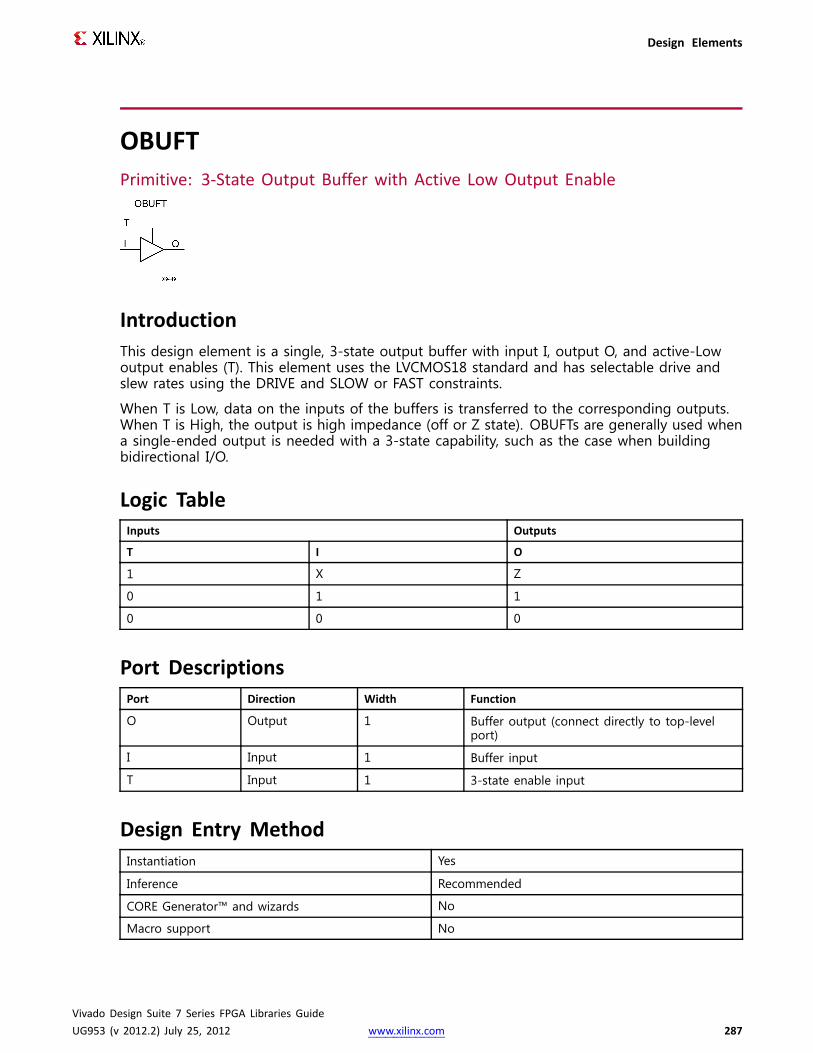
Design Elements
OBUFTPrimitive: 3-State Output Buffer with Active Low Output Enable
IntroductionThis design element is a single, 3-state output buffer with input I, output O, and active-Lowoutput enables (T). This element uses the LVCMOS18 standard and has selectable drive andslew rates using the DRIVE and SLOW or FAST constraints.
When T is Low, data on the inputs of the buffers is transferred to the corresponding outputs.When T is High, the output is high impedance (off or Z state). OBUFTs are generally used whena single-ended output is needed with a 3-state capability, such as the case when buildingbidirectional I/O.
Logic TableInputs Outputs
T I O
1 X Z
0 1 1
0 0 0
Port DescriptionsPort Direction Width Function
O Output 1 Buffer output (connect directly to top-levelport)
I Input 1 Buffer input
T Input 1 3-state enable input
Design Entry MethodInstantiation Yes
Inference Recommended
CORE Generator™ and wizards No
Macro support No
Vivado Design Suite 7 Series FPGA Libraries GuideUG953 (v 2012.2) July 25, 2012 www.xilinx.com 287
Design Elements
Available AttributesAttribute Data Type Allowed Values Default Description
DRIVE Integer 2, 4, 6, 8, 12, 16,24
12 Specifies the output current drivestrength of the I/O. It is suggestedthat you set this to the lowest settingtolerable for the design drive andtiming requirements.
IOSTANDARD String See Data Sheet "DEFAULT" Assigns an I/O standard to theelement.
SLEW String "SLOW" or "FAST" "SLOW" Specifies the slew rate of the outputdriver. See the Data Sheet forrecommendations of the best settingfor this attribute.
VHDL Instantiation TemplateUnless they already exist, copy the following two statements and paste them before the entitydeclaration.Library UNISIM;use UNISIM.vcomponents.all;
-- OBUFT: Single-ended 3-state Output Buffer-- 7 Series-- Xilinx HDL Libraries Guide, version 2012.2
OBUFT_inst : OBUFTgeneric map (
DRIVE => 12,IOSTANDARD=> "DEFAULT",SLEW=> "SLOW")
port map (O => O, -- Buffer output (connect directly to top-level port)I => I, -- Buffer inputT => T -- 3-state enable input
);
-- End of OBUFT_inst instantiation
Verilog Instantiation Template
// OBUFT: Single-ended 3-state Output Buffer// All devices// Xilinx HDL Libraries Guide, version 2012.2
OBUFT #(.DRIVE(12), // Specify the output drive strength.IOSTANDARD("DEFAULT"), // Specify the output I/O standard.SLEW("SLOW") // Specify the output slew rate
) OBUFT_inst (.O(O), // Buffer output (connect directly to top-level port).I(I), // Buffer input.T(T) // 3-state enable input
);
// End of OBUFT_inst instantiation
Vivado Design Suite 7 Series FPGA Libraries GuideUG953 (v 2012.2) July 25, 2012 www.xilinx.com 288

Design Elements
For More InformationSee the 7 series FPGA User Documentation (User Guides and Data Sheets).
Vivado Design Suite 7 Series FPGA Libraries GuideUG953 (v 2012.2) July 25, 2012 www.xilinx.com 289

Design Elements
OBUFTDSPrimitive: 3-State Output Buffer with Differential Signaling, Active-Low OutputEnable
IntroductionThis design element is an output buffer that supports low-voltage, differential signaling. For theOBUFTDS, a design level interface signal is represented as two distinct ports (O and OB), onedeemed the "master" and the other the "slave." The master and the slave are opposite phasesof the same logical signal (for example, MYNET_P and MYNET_N).
Logic TableInputs Outputs
I T O OB
X 1 Z Z
0 0 0 1
1 0 1 0
Port DescriptionsPort Direction Width Function
O Output 1 Diff_p output (connect directly to top level port)
OB Output 1 Diff_n output (connect directly to top level port)
I Input 1 Buffer input
T Input 1 3-state enable input
Design Entry MethodInstantiation Recommended
Inference No
CORE Generator™ and wizards No
Macro support No
Vivado Design Suite 7 Series FPGA Libraries GuideUG953 (v 2012.2) July 25, 2012 www.xilinx.com 290
Design Elements
Available Attributes
AttributeDataType Allowed Values Default Description
IOSTANDARD String See Data Sheet "DEFAULT" Assigns an I/O standard to the element.
SLEW String "SLOW" or "FAST" "SLOW" Specifies the slew rate of the outputdriver. Consult the product Data Sheet forrecommendations of the best setting forthis attribute.
VHDL Instantiation TemplateUnless they already exist, copy the following two statements and paste them before the entitydeclaration.Library UNISIM;use UNISIM.vcomponents.all;
-- OBUFTDS: Differential 3-state Output Buffer-- 7 Series-- Xilinx HDL Libraries Guide, version 2012.2
OBUFTDS_inst : OBUFTDSgeneric map (
IOSTANDARD=> "DEFAULT")port map (
O => O, -- Diff_p output (connect directly to top-level port)OB => OB, -- Diff_n output (connect directly to top-level port)I => I, -- Buffer inputT => T -- 3-state enable input
);
-- End of OBUFTDS_inst instantiation
Verilog Instantiation Template
// OBUFTDS: Differential 3-state Output Buffer// 7 Series// Xilinx HDL Libraries Guide, version 2012.2
OBUFTDS#(.IOSTANDARD("DEFAULT"), // Specify the output I/O standard.SLEW("SLOW") // Specify the output slew rate
) OBUFTDS_inst (.O(O), // Diff_p output (connect directly to top-level port).OB(OB), // Diff_n output (connect directly to top-level port).I(I), // Buffer input.T(T) // 3-state enable input
);
// End of OBUFTDS_inst instantiation
For More InformationSee the 7 series FPGA User Documentation (User Guides and Data Sheets).
Vivado Design Suite 7 Series FPGA Libraries GuideUG953 (v 2012.2) July 25, 2012 www.xilinx.com 291
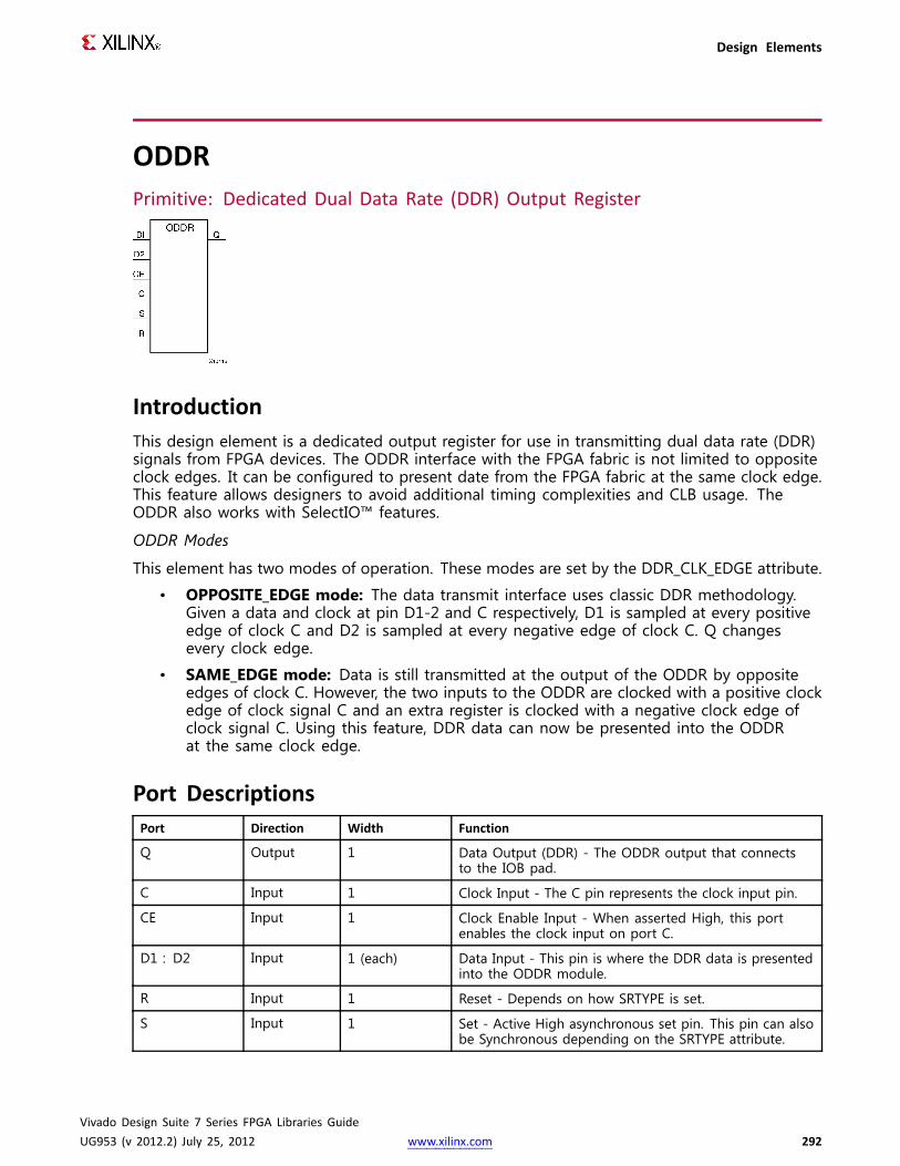
Design Elements
ODDRPrimitive: Dedicated Dual Data Rate (DDR) Output Register
IntroductionThis design element is a dedicated output register for use in transmitting dual data rate (DDR)signals from FPGA devices. The ODDR interface with the FPGA fabric is not limited to oppositeclock edges. It can be configured to present date from the FPGA fabric at the same clock edge.This feature allows designers to avoid additional timing complexities and CLB usage. TheODDR also works with SelectIO™ features.
ODDR Modes
This element has two modes of operation. These modes are set by the DDR_CLK_EDGE attribute.
• OPPOSITE_EDGE mode: The data transmit interface uses classic DDR methodology.Given a data and clock at pin D1-2 and C respectively, D1 is sampled at every positiveedge of clock C and D2 is sampled at every negative edge of clock C. Q changesevery clock edge.
• SAME_EDGE mode: Data is still transmitted at the output of the ODDR by oppositeedges of clock C. However, the two inputs to the ODDR are clocked with a positive clockedge of clock signal C and an extra register is clocked with a negative clock edge ofclock signal C. Using this feature, DDR data can now be presented into the ODDRat the same clock edge.
Port DescriptionsPort Direction Width Function
Q Output 1 Data Output (DDR) - The ODDR output that connectsto the IOB pad.
C Input 1 Clock Input - The C pin represents the clock input pin.
CE Input 1 Clock Enable Input - When asserted High, this portenables the clock input on port C.
D1 : D2 Input 1 (each) Data Input - This pin is where the DDR data is presentedinto the ODDR module.
R Input 1 Reset - Depends on how SRTYPE is set.
S Input 1 Set - Active High asynchronous set pin. This pin can alsobe Synchronous depending on the SRTYPE attribute.
Vivado Design Suite 7 Series FPGA Libraries GuideUG953 (v 2012.2) July 25, 2012 www.xilinx.com 292

Design Elements
Design Entry MethodInstantiation Recommended
Inference No
CORE Generator™ and wizards No
Macro support No
Available AttributesAttribute Data Type Allowed Values Default Description
DDR_CLK_EDGE
String "OPPOSITE_EDGE","SAME_EDGE"
"OPPOSITE_EDGE"
DDR clock mode recovery modeselection.
INIT Integer 0, 1 1 Q initialization value.
SRTYPE String "SYNC", "ASYNC" "SYNC" Set/Reset type selection.
VHDL Instantiation TemplateUnless they already exist, copy the following two statements and paste them before the entitydeclaration.Library UNISIM;use UNISIM.vcomponents.all;
-- ODDR: Output Double Data Rate Output Register with Set, Reset-- and Clock Enable.-- 7 Series-- Xilinx HDL Libraries Guide, version 2012.2
ODDR_inst : ODDRgeneric map(
DDR_CLK_EDGE=> "OPPOSITE_EDGE", -- "OPPOSITE_EDGE" or "SAME_EDGE"INIT => '0', -- Initial value for Q port ('1' or '0')SRTYPE => "SYNC") -- Reset Type ("ASYNC" or "SYNC")
port map (Q => Q, -- 1-bit DDR outputC => C, -- 1-bit clock inputCE => CE, -- 1-bit clock enable inputD1 => D1, -- 1-bit data input (positive edge)D2 => D2, -- 1-bit data input (negative edge)R => R, -- 1-bit reset inputS => S -- 1-bit set input
);
-- End of ODDR_inst instantiation
Vivado Design Suite 7 Series FPGA Libraries GuideUG953 (v 2012.2) July 25, 2012 www.xilinx.com 293

Design Elements
Verilog Instantiation Template
// ODDR: Output Double Data Rate Output Register with Set, Reset// and Clock Enable.// 7 Series// Xilinx HDL Libraries Guide, version 2012.2
ODDR#(.DDR_CLK_EDGE("OPPOSITE_EDGE"), // "OPPOSITE_EDGE" or "SAME_EDGE".INIT(1'b0), // Initial value of Q: 1'b0 or 1'b1.SRTYPE("SYNC") // Set/Reset type: "SYNC" or "ASYNC"
) ODDR_inst (.Q(Q), // 1-bit DDR output.C(C), // 1-bit clock input.CE(CE), // 1-bit clock enable input.D1(D1), // 1-bit data input (positive edge).D2(D2), // 1-bit data input (negative edge).R(R), // 1-bit reset.S(S) // 1-bit set
);
// End of ODDR_inst instantiation
For More InformationSee the 7 series FPGA User Documentation (User Guides and Data Sheets).
Vivado Design Suite 7 Series FPGA Libraries GuideUG953 (v 2012.2) July 25, 2012 www.xilinx.com 294
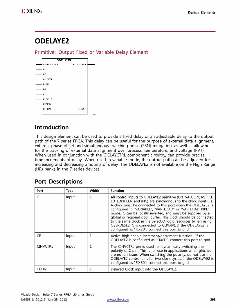
Design Elements
ODELAYE2Primitive: Output Fixed or Variable Delay Element
IntroductionThis design element can be used to provide a fixed delay or an adjustable delay to the outputpath of the 7 series FPGA. This delay can be useful for the purpose of external data alignment,external phase offset and simultaneous switching noise (SSN) mitigation, as well as allowingfor the tracking of external data alignment over process, temperature, and voltage (PVT).When used in conjunction with the IDELAYCTRL component circuitry, can provide precisetime increments of delay. When used in variable mode, the output path can be adjusted forincreasing and decreasing amounts of delay. The ODELAYE2 is not available on the High Range(HR) banks in the 7 series devices.
Port DescriptionsPort Type Width Function
C Input 1 All control inputs to ODELAYE2 primitive (CNTVALUEIN, RST, CE,LD, LDPIPEEN and INC) are synchronous to the clock input (C).A clock must be connected to this port when the ODELAYE2 isconfigured in "VARIABLE", "VAR_LOAD" or "VAR_LOAD_PIPE"mode. C can be locally inverted, and must be supplied by aglobal or regional clock buffer. This clock should be connectedto the same clock in the SelectIO logic resources (when usingOSERDESE2, C is connected to CLKDIV). If the ODELAYE2 isconfigured as "FIXED", connect this port to gnd.
CE Input 1 Active high enable increment/decrement function. If theODELAYE2 is configured as "FIXED", connect this port to gnd.
CINVCTRL Input 1 The CINVCTRL pin is used for dynamically switching thepolarity of C pin. This is for use in applications when glitchesare not an issue. When switching the polarity, do not use theODELAYE2 control pins for two clock cycles. If the ODELAYE2 isconfigured as "FIXED", connect this port to gnd.
CLKIN Input 1 Delayed Clock input into the ODELAYE2.
Vivado Design Suite 7 Series FPGA Libraries GuideUG953 (v 2012.2) July 25, 2012 www.xilinx.com 295

Design Elements
Port Type Width Function
CNTVALUEIN<4:0>
Input 5 Counter value from FPGA logic for dynamically loadabletap value input when configigured in "VAR_LOAD" or"VAR_LOAD_PIPE" modes. If the ODELAYE2 is configured as"FIXED" or "VARIABLE", connect this port to gnd.
CNTVALUEOUT<4:0>
Output 5 The CNTVALUEOUT pins are used for reporting the dynamicallyswitching value of the delay element. CNTVALUEOUTis only available when ODELAYE2 is in "VAR_LOAD" or"VAR_LOAD_PIPE" mode.
DATAOUT Output 1 Delayed data/clock from either the CLKIN or ODATAIN ports.DATAOUT connects to an I/O port in the case of data or backto the clocking structure in the case of a clock..
INC Input 1 The increment/decrement is controlled by the enable signal(CE). This interface is only available when ODELAYE2 is inVARIABLE, VAR_LOAD, or VAR_LOAD_PIPE mode.
LD Input 1 Load initial value or loaded value to the counter.
LDPIPEEN Input 1 Enable PIPELINE register to load data from LD pins.
ODATAIN Input 1 The ODATAIN input is the output data to be delayed driven bythe OSERDESE2 or output register.
REGRST Input 1 The REGRST signal is an active-high reset and is synchronous tothe input clock signal (C). When asserted, the tap value revertsto a zero state unless LDPIPEEN is also assreted in which casethe tap value results in the value on the CNTVALUEIN port.
Design Entry MethodInstantiation Yes
Inference No
CORE Generator™ and wizards Yes
Macro support No
Available AttributesAttribute Type Allowed Values Default Description
CINVCTRL_SEL STRING "FALSE", "TRUE" "FALSE" Enables the CINVCTRL_SEL pin todynamically switch the polarity ofthe C pin.
DELAY_SRC STRING "ODATAIN", "CLKIN" "ODATAIN" Select the data input source:
• "ODATAIN": ODELAYE2chain input is ODATAIN
• "CLKIN": ODELAYE2 chaininput is CLKIN
Vivado Design Suite 7 Series FPGA Libraries GuideUG953 (v 2012.2) July 25, 2012 www.xilinx.com 296

Design Elements
Attribute Type Allowed Values Default Description
HIGH_PERFORMANCE_MODE
STRING "FALSE", "TRUE" "FALSE" When TRUE, this attributereduces the output jitter. WhenFALSE, power consumption isreduced. The difference in powerconsumption is quantified in theXilinx Power Estimator tool.
ODELAY_TYPE STRING "FIXED", "VARIABLE","VAR_LOAD","VAR_LOAD_PIPE"
"FIXED" Sets the type of tap delay line.
• "FIXED": Sets a static delayvalue
• "VARIABLE":Dynamically adjust(incement/decrement)delay value
• "VAR_LOAD": Dynamicallyloads tap values
• "VAR_LOAD_PIPE":Pipelined dynamicallyloadable tap values
ODELAY_VALUE DECIMAL 0, 1, 2, 3, 4, 5, 6, 7,8, 9, 10, 11, 12, 13,14, 15, 16, 17, 18,19, 20, 21, 22, 23,24, 25, 26, 27, 28,29, 30, 31
0 Specifies the fixed number ofdelay taps in fixed mode or theinitial starting number of taps in"VARIABLE" mode (output path).When IDELAY_TYPE is set to"VAR_LOAD" or "VAR_LOAD_PIPE"mode, this value is ignored.
PIPE_SEL STRING "FALSE", "TRUE" "FALSE" Select pipelined mode.
REFCLK_FREQUENCY
1significantdigit FLOAT
190.0 to 210.0 and290.0 to 310.0
200.0 Sets the tap value (in MHz)used by the Timing Analyzerfor static timing analysis andfunctional/timing simulation. Thefrequency of REFCLK must bewithin the given datasheet rangeto guarantee the tap-delay valueand performance.
SIGNAL_PATTERN
STRING "DATA", "CLOCK" "DATA" Causes timing analysis to accountfor the appropriate amount ofdelay-chain jitter when presentedwith either a "DATA" pattern withirregular transitions or a "CLOCK"pattern with a regular rise/fallpattern.
Vivado Design Suite 7 Series FPGA Libraries GuideUG953 (v 2012.2) July 25, 2012 www.xilinx.com 297

Design Elements
VHDL Instantiation TemplateUnless they already exist, copy the following two statements and paste them before the entitydeclaration.Library UNISIM;use UNISIM.vcomponents.all;
-- ODELAYE2: Output Fixed or Variable Delay Element-- 7 Series-- Xilinx HDL Libraries Guide, version 2012.2
ODELAYE2_inst : ODELAYE2generic map (
CINVCTRL_SEL => "FALSE", -- Enable dynamic clock inversion (FALSE, TRUE)DELAY_SRC=> "ODATAIN", -- Delay input (ODATAIN, CLKIN)HIGH_PERFORMANCE_MODE=> "FALSE", -- Reduced jitter ("TRUE"), Reduced power ("FALSE")ODELAY_TYPE=> "FIXED", -- FIXED, VARIABLE, VAR_LOAD, VAR_LOAD_PIPEODELAY_VALUE=> 0, -- Output delay tap setting (0-31)PIPE_SEL => "FALSE", -- Select pipelined mode, FALSE, TRUEREFCLK_FREQUENCY=> 200.0, -- IDELAYCTRL clock input frequency in MHz (190.0-210.0).SIGNAL_PATTERN=> "DATA" -- DATA, CLOCK input signal
)port map (
CNTVALUEOUT=> CNTVALUEOUT,-- 5-bit output: Counter value outputDATAOUT=> DATAOUT, -- 1-bit output: Delayed data/clock outputC => C, -- 1-bit input: Clock inputCE => CE, -- 1-bit input: Active high enable increment/decrement inputCINVCTRL => CINVCTRL, -- 1-bit input: Dynamic clock inversion inputCLKIN => CLKIN, -- 1-bit input: Clock delay inputCNTVALUEIN => CNTVALUEIN, -- 5-bit input: Counter value inputINC => INC, -- 1-bit input: Increment / Decrement tap delay inputLD => LD, -- 1-bit input: Loads ODELAY_VALUEtap delay in VARIABLE mode, in VAR_LOADor
-- VAR_LOAD_PIPE mode, loads the value of CNTVALUEIN
LDPIPEEN => LDPIPEEN, -- 1-bit input: Enables the pipeline register to load dataODATAIN => ODATAIN, -- 1-bit input: Output delay data inputREGRST=> REGRST -- 1-bit input: Active-high reset tap-delay input
);
-- End of ODELAYE2_inst instantiation
Vivado Design Suite 7 Series FPGA Libraries GuideUG953 (v 2012.2) July 25, 2012 www.xilinx.com 298
Design Elements
Verilog Instantiation Template
// ODELAYE2: Output Fixed or Variable Delay Element// 7 Series// Xilinx HDL Libraries Guide, version 2012.2
(* IODELAY_GROUP= <iodelay_group_name> *) // Specifies group name for associated IDELAYs/ODELAYs and IDELAYCTRL
ODELAYE2#(.CINVCTRL_SEL("FALSE"), // Enable dynamic clock inversion (FALSE, TRUE).DELAY_SRC("ODATAIN"), // Delay input (ODATAIN, CLKIN).HIGH_PERFORMANCE_MODE("FALSE"), // Reduced jitter ("TRUE"), Reduced power ("FALSE").ODELAY_TYPE("FIXED"), // FIXED, VARIABLE, VAR_LOAD, VAR_LOAD_PIPE.ODELAY_VALUE(0), // Output delay tap setting (0-31).PIPE_SEL("FALSE"), // Select pipelined mode, FALSE, TRUE.REFCLK_FREQUENCY(200.0), // IDELAYCTRL clock input frequency in MHz (190.0-210.0)..SIGNAL_PATTERN("DATA") // DATA, CLOCK input signal
)ODELAYE2_inst (
.CNTVALUEOUT(CNTVALUEOUT),// 5-bit output: Counter value output
.DATAOUT(DATAOUT), // 1-bit output: Delayed data/clock output
.C(C), // 1-bit input: Clock input
.CE(CE), // 1-bit input: Active high enable increment/decrement input
.CINVCTRL(CINVCTRL), // 1-bit input: Dynamic clock inversion input
.CLKIN(CLKIN), // 1-bit input: Clock delay input
.CNTVALUEIN(CNTVALUEIN), // 5-bit input: Counter value input
.INC(INC), // 1-bit input: Increment / Decrement tap delay input
.LD(LD), // 1-bit input: Loads ODELAY_VALUEtap delay in VARIABLE mode, in VAR_LOADor// VAR_LOAD_PIPE mode, loads the value of CNTVALUEIN
.LDPIPEEN(LDPIPEEN), // 1-bit input: Enables the pipeline register to load data
.ODATAIN(ODATAIN), // 1-bit input: Output delay data input
.REGRST(REGRST) // 1-bit input: Active-high reset tap-delay input);
// End of ODELAYE2_inst instantiation
For More Information• See the 7 series FPGA SelectIO Resources User Guide (UG471).
• See the 7 series FPGA User Documentation (User Guides and Data Sheets).
Vivado Design Suite 7 Series FPGA Libraries GuideUG953 (v 2012.2) July 25, 2012 www.xilinx.com 299
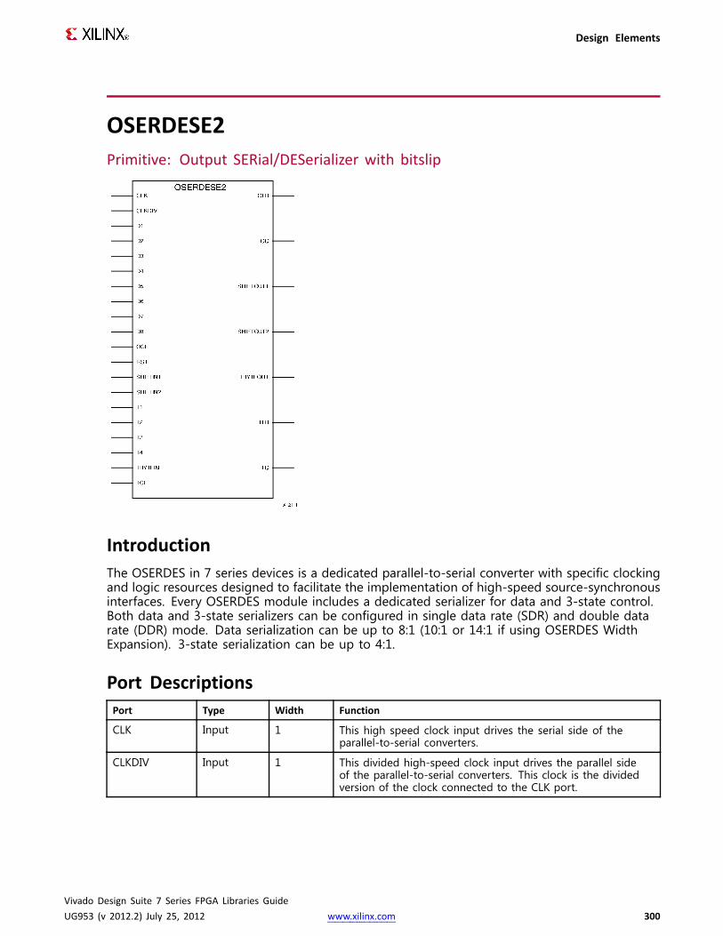
Design Elements
OSERDESE2Primitive: Output SERial/DESerializer with bitslip
IntroductionThe OSERDES in 7 series devices is a dedicated parallel-to-serial converter with specific clockingand logic resources designed to facilitate the implementation of high-speed source-synchronousinterfaces. Every OSERDES module includes a dedicated serializer for data and 3-state control.Both data and 3-state serializers can be configured in single data rate (SDR) and double datarate (DDR) mode. Data serialization can be up to 8:1 (10:1 or 14:1 if using OSERDES WidthExpansion). 3-state serialization can be up to 4:1.
Port DescriptionsPort Type Width Function
CLK Input 1 This high speed clock input drives the serial side of theparallel-to-serial converters.
CLKDIV Input 1 This divided high-speed clock input drives the parallel sideof the parallel-to-serial converters. This clock is the dividedversion of the clock connected to the CLK port.
Vivado Design Suite 7 Series FPGA Libraries GuideUG953 (v 2012.2) July 25, 2012 www.xilinx.com 300
Design Elements
Port Type Width Function
D1 - D8 Input 1 All incoming parallel data enters the OSERDES module throughports D1 to D8. These ports are connected to the FPGAfabric, and can be configured from two to eight bits (i.e., a8:1 serialization). Bit widths greater than six (up to 14) can besupported by using a second OSERDES in SLAVE mode.
OCE Input 1 OCE is an active High clock enable for the data path.
OFB Output 1 The output feedback port (OFB) is the serial (high-speed) dataoutput port of the OSERDESE2.
OQ Output 1 The OQ port is the data output port of the OSERDES module.Data at the input port D1 will appear first at OQ. This portconnects the output of the data parallel-to-serial converterto the data input of the IOB. This port can not drive theODELAYE2; the OFB pin must be used.
RST Input 1 The reset input causes the outputs of all data flip-flops in theCLK and CLKDIV domains to be driven Low asynchronously.OSERDES circuits running in the CLK domain where timing iscritical use an internal, dedicated circuit to retime the RST inputto produce a reset signal synchronous to the CLK domain.Similarly, there is a dedicated circuit to retime the RST inputto produce a reset signal synchronous to the CLKDIV domain.Because there are OSERDES circuits that retime the RST input,the user is only required to provide a reset pulse to the RSTinput that meets timing on the CLKDIV frequency domain(synchronous to CLKDIV). Therefore, RST should be drivenHigh for a minimum of one CLKDIV cycle. When building aninterface consisting of multiple OSERDES ports, all OSERDESports must be synchronized. The internal retiming of the RSTinput is designed so that all OSERDES blocks that receive thesame reset pulse come out of reset synchronized with oneanother.
SHIFTIN1 /SHIFTIN2
Input 1 Cascade Input for data input expansion. Connect toSHIFTOUT1/2 of slave.
SHIFTOUT1 /SHIFTOUT2
Output 1 Cascade out for data input expansion. Connect to SHIFTIN1/2of master.
TBYTEIN Input 1 Byte group tristate input from source
TBYTEOUT Output 1 Byte group tristate output to IOB
TCE Input 1 TCE is an active High clock enable for the 3-state control path.
TFB Output 1 This port is the 3-state control output of the OSERDESmodule sent to the ODELAYE2. When used, this port connectsthe output of the 3-state parallel-to-serial converter to thecontrol/3-state input of the ODELAYE2.
TQ Output 1 This port is the 3-state control output of the OSERDES module.When used, this port connects the output of the 3-stateparallel-to-serial converter to the control/3-state input of theIOB.
T1 - T4 Input 1 All parallel 3-state signals enter the OSERDES module throughports T1 to T4. The ports are connected to the FPGA fabric,and can be configured as one, two, or four bits.
Vivado Design Suite 7 Series FPGA Libraries GuideUG953 (v 2012.2) July 25, 2012 www.xilinx.com 301
Design Elements
Design Entry MethodInstantiation Yes
Inference No
CORE Generator™ and wizards Yes
Macro support No
Available AttributesAttribute Type Allowed Values Default Description
DATA_RATE_OQ STRING "DDR", "SDR" "DDR" The DATA_RATE_OQ attributedefines whether data is processedas single data rate (SDR) or doubledata rate (DDR).
DATA_RATE_TQ STRING "DDR", "BUF", "SDR" "DDR" The DATA_RATE_TQ attributedefines whether 3-state control isto be processed as single data rate(SDR) or double data rate (DDR).
DATA_WIDTH DECIMAL 4, 2, 3, 5, 6, 7, 8, 10,14
4 The DATA_WIDTH attribute definesthe parallel data input width of theparallel-to-serial converter. Thepossible values for this attributedepend on the DATA_RATE_OQattribute. When DATA_RATE_OQis set to SDR, the possible valuesfor the DATA_WIDTH attributeare 2, 3, 4, 5, 6, 7, and 8.When DATA_RATE_OQ is set toDDR, the possible values for theDATA_WIDTH attribute are 4, 6, 8,10 and 14. When the DATA_WIDTHis set to widths larger than eight,a pair of OSERDES must beconfigured into a master-slaveconfiguration.
INIT_OQ BINARY 1'b0 to 1'b1 1'b0 Defines the initial value of OQoutput.
INIT_TQ BINARY 1'b0 to 1'b1 1'b0 Defines the initial value of TQoutput.
SERDES_MODE STRING "MASTER", "SLAVE" "MASTER" The SERDES_MODE attributedefines whether the OSERDESmodule is a master or slave whenusing width expansion.
SRVAL_OQ BINARY 1'b0 to 1'b1 1'b0 Defines the value of OQ outputswhen the SR is invoked.
SRVAL_TQ BINARY 1'b0 to 1'b1 1'b0 Defines the value of YQ outputswhen the SR is invoked.
Vivado Design Suite 7 Series FPGA Libraries GuideUG953 (v 2012.2) July 25, 2012 www.xilinx.com 302
Design Elements
Attribute Type Allowed Values Default Description
TBYTE_CTL STRING "FALSE", "TRUE" "FALSE" Enable Tristate BYTE operationfor DDR3 mode. This allows thetristate signal to take value fromone of the tristate outputs whichis acting as a source.
TBYTE_SRC STRING "FALSE", "TRUE" "FALSE" Enable OSERDES to act as a sourcefor Tristate Byte operation in DDR3mode.
TRISTATE_WIDTH
DECIMAL 4, 1 4 The TRISTATE_WIDTH attributedefines the parallel 3-state inputwidth of the 3-state controlparallel-to-serial converter. Thepossible values for this attributedepend on the DATA_RATE_TQattribute. When DATA_RATE_TQis set to SDR or BUF, theTRISTATE_WIDTH attribute can onlybe set to 1. When DATA_RATE_TQis set to DDR, the possible valuesfor the TRISTATE_WIDTH attributeis 4. TRISTATE_WIDTH cannot beset to widths larger than 4. Whena DATA_WIDTH is larger than four,set the TRISTATE_WIDTH to 1.
VHDL Instantiation TemplateUnless they already exist, copy the following two statements and paste them before the entitydeclaration.Library UNISIM;use UNISIM.vcomponents.all;
-- OSERDESE2: Output SERial/DESerializer with bitslip-- 7 Series-- Xilinx HDL Libraries Guide, version 2012.2
OSERDESE2_inst : OSERDESE2generic map (
DATA_RATE_OQ=> "DDR", -- DDR, SDRDATA_RATE_TQ=> "DDR", -- DDR, BUF, SDRDATA_WIDTH=> 4, -- Parallel data width (2-8,10,14)INIT_OQ => '0', -- Initial value of OQ output (1'b0,1'b1)INIT_TQ => '0', -- Initial value of TQ output (1'b0,1'b1)SERDES_MODE=> "MASTER", -- MASTER, SLAVESRVAL_OQ=> '0', -- OQ output value when SR is used (1'b0,1'b1)SRVAL_TQ=> '0', -- TQ output value when SR is used (1'b0,1'b1)TBYTE_CTL => "FALSE", -- Enable tristate byte operation (FALSE, TRUE)TBYTE_SRC=> "FALSE", -- Tristate byte source (FALSE, TRUE)TRISTATE_WIDTH => 4 -- 3-state converter width (1,4)
)port map (
OFB => OFB, -- 1-bit output: Feedback path for dataOQ => OQ, -- 1-bit output: Data path output-- SHIFTOUT1 / SHIFTOUT2: 1-bit (each) output: Data output expansion (1-bit each)SHIFTOUT1 => SHIFTOUT1,SHIFTOUT2 => SHIFTOUT2,TBYTEOUT=> TBYTEOUT, -- 1-bit output: Byte group tristateTFB => TFB, -- 1-bit output: 3-state controlTQ => TQ, -- 1-bit output: 3-state control
Vivado Design Suite 7 Series FPGA Libraries GuideUG953 (v 2012.2) July 25, 2012 www.xilinx.com 303
Design Elements
CLK => CLK, -- 1-bit input: High speed clockCLKDIV => CLKDIV, -- 1-bit input: Divided clock-- D1 - D8: 1-bit (each) input: Parallel data inputs (1-bit each)D1 => D1,D2 => D2,D3 => D3,D4 => D4,D5 => D5,D6 => D6,D7 => D7,D8 => D8,OCE => OCE, -- 1-bit input: Output data clock enableRST => RST, -- 1-bit input: Reset-- SHIFTIN1 / SHIFTIN2: 1-bit (each) input: Data input expansion (1-bit each)SHIFTIN1 => SHIFTIN1,SHIFTIN2 => SHIFTIN2,-- T1 - T4: 1-bit (each) input: Parallel 3-state inputsT1 => T1,T2 => T2,T3 => T3,T4 => T4,TBYTEIN => TBYTEIN, -- 1-bit input: Byte group tristateTCE => TCE -- 1-bit input: 3-state clock enable
);
-- End of OSERDESE2_inst instantiation
Vivado Design Suite 7 Series FPGA Libraries GuideUG953 (v 2012.2) July 25, 2012 www.xilinx.com 304

Design Elements
Verilog Instantiation Template
// OSERDESE2: Output SERial/DESerializer with bitslip// 7 Series// Xilinx HDL Libraries Guide, version 2012.2
OSERDESE2#(.DATA_RATE_OQ("DDR"), // DDR, SDR.DATA_RATE_TQ("DDR"), // DDR, BUF, SDR.DATA_WIDTH(4), // Parallel data width (2-8,10,14).INIT_OQ(1'b0), // Initial value of OQ output (1'b0,1'b1).INIT_TQ(1'b0), // Initial value of TQ output (1'b0,1'b1).SERDES_MODE("MASTER"), // MASTER, SLAVE.SRVAL_OQ(1'b0), // OQ output value when SR is used (1'b0,1'b1).SRVAL_TQ(1'b0), // TQ output value when SR is used (1'b0,1'b1).TBYTE_CTL("FALSE"), // Enable tristate byte operation (FALSE, TRUE).TBYTE_SRC("FALSE"), // Tristate byte source (FALSE, TRUE).TRISTATE_WIDTH(4) // 3-state converter width (1,4)
)OSERDESE2_inst (
.OFB(OFB), // 1-bit output: Feedback path for data
.OQ(OQ), // 1-bit output: Data path output// SHIFTOUT1 / SHIFTOUT2: 1-bit (each) output: Data output expansion (1-bit each).SHIFTOUT1(SHIFTOUT1),.SHIFTOUT2(SHIFTOUT2),.TBYTEOUT(TBYTEOUT), // 1-bit output: Byte group tristate.TFB(TFB), // 1-bit output: 3-state control.TQ(TQ), // 1-bit output: 3-state control.CLK(CLK), // 1-bit input: High speed clock.CLKDIV(CLKDIV), // 1-bit input: Divided clock// D1 - D8: 1-bit (each) input: Parallel data inputs (1-bit each).D1(D1),.D2(D2),.D3(D3),.D4(D4),.D5(D5),.D6(D6),.D7(D7),.D8(D8),.OCE(OCE), // 1-bit input: Output data clock enable.RST(RST), // 1-bit input: Reset// SHIFTIN1 / SHIFTIN2: 1-bit (each) input: Data input expansion (1-bit each).SHIFTIN1(SHIFTIN1),.SHIFTIN2(SHIFTIN2),// T1 - T4: 1-bit (each) input: Parallel 3-state inputs.T1(T1),.T2(T2),.T3(T3),.T4(T4),.TBYTEIN(TBYTEIN), // 1-bit input: Byte group tristate.TCE(TCE) // 1-bit input: 3-state clock enable
);
// End of OSERDESE2_inst instantiation
For More Information• See the 7 series FPGA SelectIO Resources User Guide (UG471).
• See the 7 series FPGA User Documentation (User Guides and Data Sheets).
Vivado Design Suite 7 Series FPGA Libraries GuideUG953 (v 2012.2) July 25, 2012 www.xilinx.com 305

Design Elements
OUT_FIFOPrimitive: Output First-In, First-Out (FIFO) Buffer
The Output FIFO is a new resource located next to the I/O. This dedicated hardware is designedto help transition the data from fabric to the I/O, ODDR or OSERDES. It has two basic modesthe first is a 4x4 mode where the data coming into the FIFO goes out at the same rate. Thesecond mode is a 8x4 mode where the data coming out is serialized by a factor of 2. In otherwords in 8x4 mode 8 bits go to the OUT_FIFO and 4 bits come out.
The Output FIFO is a new resource located next to the I/O. This dedicated hardware is designedto help transition the data from fabric to the I/O, ODDR or OSERDES. It has two basic modes thefirst is a 4x4 mode where the data coming into the FIFO goes out at the same rate. The secondmode is a 8x4 mode where the data coming out is serialized by a factor of 2. In other words in8x4 mode 8 bits go to the OUT_FIFO and 4 bits come out. Features of this component include:
• Array dimensions: 80 wide, 8 deep (8x4 mode); 40 wide, 8 deep (4x4 mode)
• Empty and Full flags
• Programmable Almost Empty and Almost Full flags
Vivado Design Suite 7 Series FPGA Libraries GuideUG953 (v 2012.2) July 25, 2012 www.xilinx.com 306

Design Elements
Port DescriptionsPort Type Width Function
ALMOSTEMPTY Output 1 Active high output flag indicating the FIFO is almost empty.The threshold of the almost empty flag is set by theALMOST_EMPTY_VALUE attribute.
ALMOSTFULL Output 1 Active high output flag indicating the FIFO is almost full.The threshold of the almost empty flag is set by theALMOST_FULL_VALUE attribute.
D0<7:0> Input 8 Channel 0 input bus.
D1<7:0> Input 8 Channel 1 input bus.
D2<7:0> Input 8 Channel 2 input bus.
D3<7:0> Input 8 Channel 3 input bus.
D4<7:0> Input 8 Channel 4 input bus.
D5<7:0> Input 8 Channel 5 input bus.
D6<7:0> Input 8 Channel 6 input bus.
D7<7:0> Input 8 Channel 7 input bus.
D8<7:0> Input 8 Channel 8 input bus.
D9<7:0> Input 8 Channel 9 input bus.
EMPTY Output 1 Active high output flag indicating the FIFO is empty.
FULL Output 1 Active high output flag indicating the FIFO is full.
Q0<3:0> Output 4 Channel 0 output bus.
Q1<3:0> Output 4 Channel 1 output bus.
Q2<3:0> Output 4 Channel 2 output bus.
Q3<3:0> Output 4 Channel 3 output bus.
Q4<3:0> Output 4 Channel 4 output bus.
Q5<7:0> Output 8 Channel 5 output bus.
Q6<7:0> Output 8 Channel 6 output bus.
Q7<3:0> Output 4 Channel 7 output bus.
Q8<3:0> Output 4 Channel 8 output bus.
Q9<3:0> Output 4 Channel 9 output bus.
RDCLK Input 1 Read clock
RDEN Input 1 Active high read enable
RESET Input 1 Active high asynchrnous reset
WRCLK Input 1 Write clock
WREN Input 1 Active high write enable
Vivado Design Suite 7 Series FPGA Libraries GuideUG953 (v 2012.2) July 25, 2012 www.xilinx.com 307
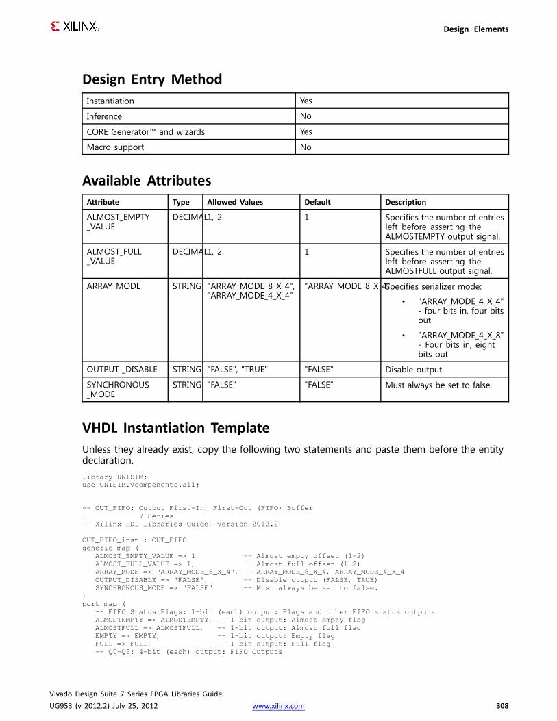
Design Elements
Design Entry MethodInstantiation Yes
Inference No
CORE Generator™ and wizards Yes
Macro support No
Available AttributesAttribute Type Allowed Values Default Description
ALMOST_EMPTY_VALUE
DECIMAL1, 2 1 Specifies the number of entriesleft before asserting theALMOSTEMPTY output signal.
ALMOST_FULL_VALUE
DECIMAL1, 2 1 Specifies the number of entriesleft before asserting theALMOSTFULL output signal.
ARRAY_MODE STRING "ARRAY_MODE_8_X_4","ARRAY_MODE_4_X_4"
"ARRAY_MODE_8_X_4"Specifies serializer mode:
• "ARRAY_MODE_4_X_4"- four bits in, four bitsout
• "ARRAY_MODE_4_X_8"- Four bits in, eightbits out
OUTPUT _DISABLE STRING "FALSE", "TRUE" "FALSE" Disable output.
SYNCHRONOUS_MODE
STRING "FALSE" "FALSE" Must always be set to false.
VHDL Instantiation TemplateUnless they already exist, copy the following two statements and paste them before the entitydeclaration.Library UNISIM;use UNISIM.vcomponents.all;
-- OUT_FIFO: Output First-In, First-Out (FIFO) Buffer-- 7 Series-- Xilinx HDL Libraries Guide, version 2012.2
OUT_FIFO_inst : OUT_FIFOgeneric map (
ALMOST_EMPTY_VALUE=> 1, -- Almost empty offset (1-2)ALMOST_FULL_VALUE=> 1, -- Almost full offset (1-2)ARRAY_MODE=> "ARRAY_MODE_8_X_4", -- ARRAY_MODE_8_X_4,ARRAY_MODE_4_X_4OUTPUT_DISABLE=> "FALSE", -- Disable output (FALSE, TRUE)SYNCHRONOUS_MODE=> "FALSE" -- Must always be set to false.
)port map (
-- FIFO Status Flags: 1-bit (each) output: Flags and other FIFO status outputsALMOSTEMPTY=> ALMOSTEMPTY,-- 1-bit output: Almost empty flagALMOSTFULL=> ALMOSTFULL, -- 1-bit output: Almost full flagEMPTY=> EMPTY, -- 1-bit output: Empty flagFULL => FULL, -- 1-bit output: Full flag-- Q0-Q9: 4-bit (each) output: FIFO Outputs
Vivado Design Suite 7 Series FPGA Libraries GuideUG953 (v 2012.2) July 25, 2012 www.xilinx.com 308
Design Elements
Q0 => Q0, -- 4-bit output: Channel 0 output busQ1 => Q1, -- 4-bit output: Channel 1 output busQ2 => Q2, -- 4-bit output: Channel 2 output busQ3 => Q3, -- 4-bit output: Channel 3 output busQ4 => Q4, -- 4-bit output: Channel 4 output busQ5 => Q5, -- 8-bit output: Channel 5 output busQ6 => Q6, -- 8-bit output: Channel 6 output busQ7 => Q7, -- 4-bit output: Channel 7 output busQ8 => Q8, -- 4-bit output: Channel 8 output busQ9 => Q9, -- 4-bit output: Channel 9 output bus-- D0-D9: 8-bit (each) input: FIFO inputsD0 => D0, -- 8-bit input: Channel 0 input busD1 => D1, -- 8-bit input: Channel 1 input busD2 => D2, -- 8-bit input: Channel 2 input busD3 => D3, -- 8-bit input: Channel 3 input busD4 => D4, -- 8-bit input: Channel 4 input busD5 => D5, -- 8-bit input: Channel 5 input busD6 => D6, -- 8-bit input: Channel 6 input busD7 => D7, -- 8-bit input: Channel 7 input busD8 => D8, -- 8-bit input: Channel 8 input busD9 => D9, -- 8-bit input: Channel 9 input bus-- FIFO Control Signals: 1-bit (each) input: Clocks, Resets and EnablesRDCLK => RDCLK, -- 1-bit input: Read clockRDEN=> RDEN, -- 1-bit input: Read enableRESET => RESET, -- 1-bit input: Active high resetWRCLK=> WRCLK, -- 1-bit input: Write clockWREN=> WREN -- 1-bit input: Write enable
);
-- End of OUT_FIFO_inst instantiation
Vivado Design Suite 7 Series FPGA Libraries GuideUG953 (v 2012.2) July 25, 2012 www.xilinx.com 309
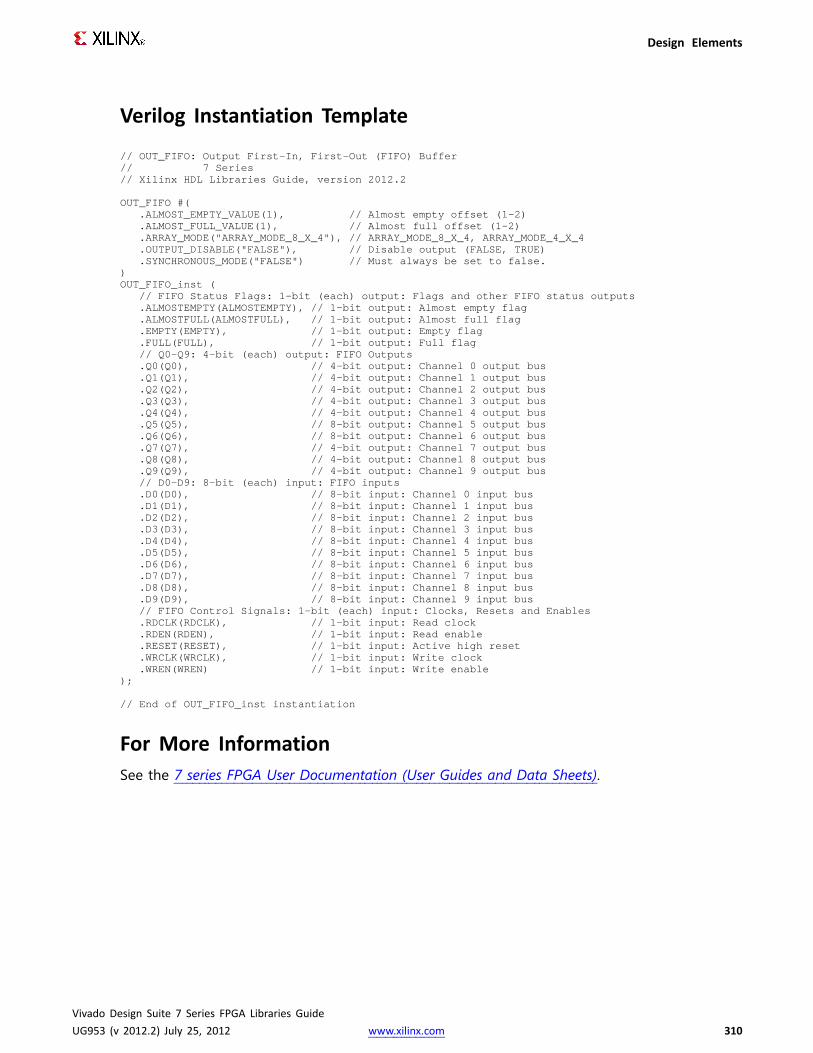
Design Elements
Verilog Instantiation Template
// OUT_FIFO: Output First-In, First-Out (FIFO) Buffer// 7 Series// Xilinx HDL Libraries Guide, version 2012.2
OUT_FIFO #(.ALMOST_EMPTY_VALUE(1), // Almost empty offset (1-2).ALMOST_FULL_VALUE(1), // Almost full offset (1-2).ARRAY_MODE("ARRAY_MODE_8_X_4"), // ARRAY_MODE_8_X_4,ARRAY_MODE_4_X_4.OUTPUT_DISABLE("FALSE"), // Disable output (FALSE, TRUE).SYNCHRONOUS_MODE("FALSE") // Must always be set to false.
)OUT_FIFO_inst (
// FIFO Status Flags: 1-bit (each) output: Flags and other FIFO status outputs.ALMOSTEMPTY(ALMOSTEMPTY),// 1-bit output: Almost empty flag.ALMOSTFULL(ALMOSTFULL), // 1-bit output: Almost full flag.EMPTY(EMPTY), // 1-bit output: Empty flag.FULL(FULL), // 1-bit output: Full flag// Q0-Q9: 4-bit (each) output: FIFO Outputs.Q0(Q0), // 4-bit output: Channel 0 output bus.Q1(Q1), // 4-bit output: Channel 1 output bus.Q2(Q2), // 4-bit output: Channel 2 output bus.Q3(Q3), // 4-bit output: Channel 3 output bus.Q4(Q4), // 4-bit output: Channel 4 output bus.Q5(Q5), // 8-bit output: Channel 5 output bus.Q6(Q6), // 8-bit output: Channel 6 output bus.Q7(Q7), // 4-bit output: Channel 7 output bus.Q8(Q8), // 4-bit output: Channel 8 output bus.Q9(Q9), // 4-bit output: Channel 9 output bus// D0-D9: 8-bit (each) input: FIFO inputs.D0(D0), // 8-bit input: Channel 0 input bus.D1(D1), // 8-bit input: Channel 1 input bus.D2(D2), // 8-bit input: Channel 2 input bus.D3(D3), // 8-bit input: Channel 3 input bus.D4(D4), // 8-bit input: Channel 4 input bus.D5(D5), // 8-bit input: Channel 5 input bus.D6(D6), // 8-bit input: Channel 6 input bus.D7(D7), // 8-bit input: Channel 7 input bus.D8(D8), // 8-bit input: Channel 8 input bus.D9(D9), // 8-bit input: Channel 9 input bus// FIFO Control Signals: 1-bit (each) input: Clocks, Resets and Enables.RDCLK(RDCLK), // 1-bit input: Read clock.RDEN(RDEN), // 1-bit input: Read enable.RESET(RESET), // 1-bit input: Active high reset.WRCLK(WRCLK), // 1-bit input: Write clock.WREN(WREN) // 1-bit input: Write enable
);
// End of OUT_FIFO_inst instantiation
For More InformationSee the 7 series FPGA User Documentation (User Guides and Data Sheets).
Vivado Design Suite 7 Series FPGA Libraries GuideUG953 (v 2012.2) July 25, 2012 www.xilinx.com 310
Design Elements
PHASER_INPrimitive: Phaser in
IntroductionPHASER_IN is designed to work with other PHASER elements to handle data alignment andcapture for high-speed memory interfaces. Its only intended use is by the Memory InterfaceGenerator (MIG) and is not intended to be instantiated, used or modified outside of Xilinxgenerated IP.
Design Entry MethodInstantiation No
Inference No
CORE Generator™ and wizards Yes
Macro support No
For More InformationSee the 7 series FPGA User Documentation (User Guides and Data Sheets).
Vivado Design Suite 7 Series FPGA Libraries GuideUG953 (v 2012.2) July 25, 2012 www.xilinx.com 311

Design Elements
PHASER_IN_PHYPrimitive: Phaser in phy
IntroductionPHASER_IN_PHY is designed to work with other PHASER elements to handle data alignmentand capture for high-speed memory interfaces. Its only intended use is by the MemoryInterface Generator(MIG) and is not intended to be instantiated, used or modified outside ofXilinx generated IP.
Design Entry MethodInstantiation No
Inference No
CORE Generator™ and wizards Yes
Macro support No
For More InformationSee the 7 series FPGA User Documentation (User Guides and Data Sheets).
Vivado Design Suite 7 Series FPGA Libraries GuideUG953 (v 2012.2) July 25, 2012 www.xilinx.com 312

Design Elements
PHASER_OUTPrimitive: Phaser out.
IntroductionPHASER_OUT is designed to work with other PHASER elements to handle data alignmentand capture for high-speed memory interfaces. Its only intended use is by the MemoryInterface Generator (MIG) and is not intended to be instantiated, used or modified outside ofXilinx generated IP.
Design Entry MethodInstantiation No
Inference No
CORE Generator™ and wizards Yes
Macro support No
For More InformationSee the 7 series FPGA User Documentation (User Guides and Data Sheets).
Vivado Design Suite 7 Series FPGA Libraries GuideUG953 (v 2012.2) July 25, 2012 www.xilinx.com 313
Design Elements
PHASER_OUT_PHYPrimitive: Phaser out phy.
IntroductionPHASER_OUT_PHY is designed to work with other PHASER elements to handle data alignmentand capture for high-speed memory interfaces. Its only intended use is by the MemoryInterface Generator (MIG) and is not intended to be instantiated, used or modified outside ofXilinx generated IP.
Design Entry MethodInstantiation No
Inference No
CORE Generator™ and wizards Yes
Macro support No
For More InformationSee the 7 series FPGA User Documentation (User Guides and Data Sheets).
Vivado Design Suite 7 Series FPGA Libraries GuideUG953 (v 2012.2) July 25, 2012 www.xilinx.com 314

Design Elements
PHASER_REFPrimitive: Phaser out.
IntroductionPHASER_REF is designed to work with other PHASER elements to handle data alignment andcapture for high-speed memory interfaces. Its only intended use is by the Memory InterfaceGenerator (MIG) and is not intended to be instantiated, used or modified outside of Xilinxgenerated IP.
Design Entry MethodInstantiation No
Inference No
CORE Generator™ and wizards Yes
Macro support No
For More InformationSee the 7 series FPGA User Documentation (User Guides and Data Sheets).
Vivado Design Suite 7 Series FPGA Libraries GuideUG953 (v 2012.2) July 25, 2012 www.xilinx.com 315

Design Elements
PHY_CONTROLPrimitive: Phaser out.
IntroductionPHY_CONTROL is designed to work with other PHASER elements to handle data alignmentand capture for high-speed memory interfaces. Its only intended use is by the MemoryInterface Generator (MIG) and is not intended to be instantiated, used or modified outside ofXilinx generated IP.
Design Entry MethodInstantiation No
Inference No
CORE Generator™ and wizards Yes
Macro support No
For More InformationSee the 7 series FPGA User Documentation (User Guides and Data Sheets).
Vivado Design Suite 7 Series FPGA Libraries GuideUG953 (v 2012.2) July 25, 2012 www.xilinx.com 316
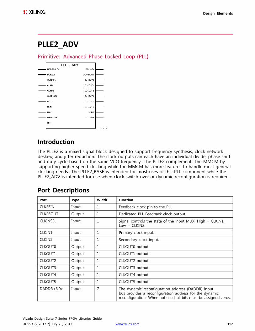
Design Elements
PLLE2_ADVPrimitive: Advanced Phase Locked Loop (PLL)
IntroductionThe PLLE2 is a mixed signal block designed to support frequency synthesis, clock networkdeskew, and jitter reduction. The clock outputs can each have an individual divide, phase shiftand duty cycle based on the same VCO frequency. The PLLE2 complements the MMCM bysupporting higher speed clocking while the MMCM has more features to handle most generalclocking needs. The PLLE2_BASE is intended for most uses of this PLL component while thePLLE2_ADV is intended for use when clock switch-over or dynamic reconfiguration is required.
Port DescriptionsPort Type Width Function
CLKFBIN Input 1 Feedback clock pin to the PLL
CLKFBOUT Output 1 Dedicated PLL Feedback clock output
CLKINSEL Input 1 Signal controls the state of the input MUX, High = CLKIN1,Low = CLKIN2.
CLKIN1 Input 1 Primary clock input.
CLKIN2 Input 1 Secondary clock input.
CLKOUT0 Output 1 CLKOUT0 output
CLKOUT1 Output 1 CLKOUT1 output
CLKOUT2 Output 1 CLKOUT2 output
CLKOUT3 Output 1 CLKOUT3 output
CLKOUT4 Output 1 CLKOUT4 output
CLKOUT5 Output 1 CLKOUT5 output
DADDR<6:0> Input 7 The dynamic reconfiguration address (DADDR) inputbus provides a reconfiguration address for the dynamicreconfiguration. When not used, all bits must be assigned zeros.
Vivado Design Suite 7 Series FPGA Libraries GuideUG953 (v 2012.2) July 25, 2012 www.xilinx.com 317
Design Elements
Port Type Width Function
DCLK Input 1 The DCLK signal is the reference clock for the dynamicreconfiguration port.
DEN Input 1 The dynamic reconfiguration enable (DEN) provides the enablecontrol signal to access the dynamic reconfiguration feature.When the dynamic reconfiguration feature is not used, DENmust be tied Low.
DI<15:0> Input 16 The dynamic reconfiguration data input (DI) bus providesreconfiguration data. When not used, all bits must be set tozero.
DO<15:0> Output 16 The dynamic reconfiguration output bus provides PLL dataoutput when using dynamic reconfiguration.
DRDY Output 1 The dynamic reconfiguration ready output (DRDY) providesthe response to the DEN signal for the PLLs dynamicreconfiguration feature.
DWE Input 1 The dynamic reconfiguration write enable (DWE) input pinprovides the write enable control signal to write the DI datainto the DADDR address. When not used, it must be tied Low.
PWRDWN Input 1 Powers down instantiated but unused PLLs.
RST Input 1 The RST signal is an asynchronous reset for the PLL. The PLLwill synchronously re-enable itself when this signal is releasedand go through a new phase alignment and lock cycle. Areset is required when the input clock conditions change (e.g.,frequency).
Status Ports Output 1 An output from the PLL that indicates when the PLL hasachieved phase alignment within a predefined window andfrequency matching within a predefined PPM range. The PLLautomatically locks after power on, no extra reset is required.LOCKED will be deasserted if the input clock stops or the phasealignment is violated (e.g., input clock phase shift). The PLLautomatically reacquires lock after LOCKED is deasserted.
Design Entry MethodInstantiation Yes
Inference No
CORE Generator™ and wizards Yes
Macro support No
Vivado Design Suite 7 Series FPGA Libraries GuideUG953 (v 2012.2) July 25, 2012 www.xilinx.com 318
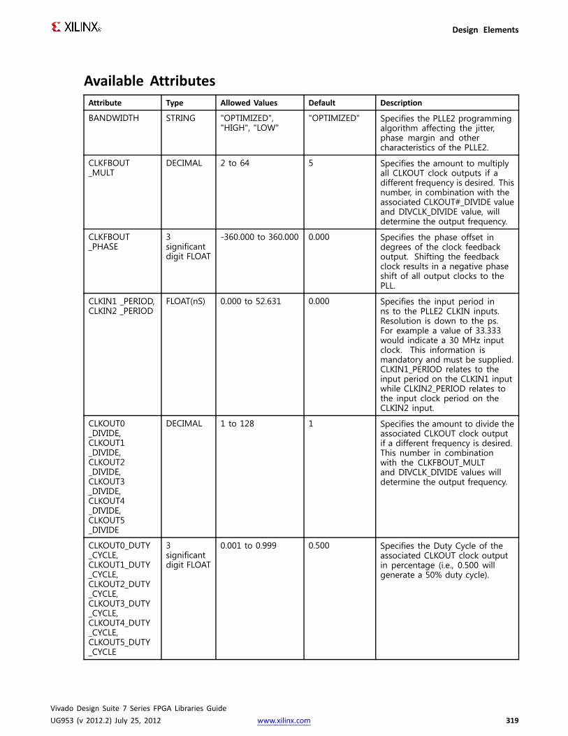
Design Elements
Available AttributesAttribute Type Allowed Values Default Description
BANDWIDTH STRING "OPTIMIZED","HIGH", "LOW"
"OPTIMIZED" Specifies the PLLE2 programmingalgorithm affecting the jitter,phase margin and othercharacteristics of the PLLE2.
CLKFBOUT_MULT
DECIMAL 2 to 64 5 Specifies the amount to multiplyall CLKOUT clock outputs if adifferent frequency is desired. Thisnumber, in combination with theassociated CLKOUT#_DIVIDE valueand DIVCLK_DIVIDE value, willdetermine the output frequency.
CLKFBOUT_PHASE
3significantdigit FLOAT
-360.000 to 360.000 0.000 Specifies the phase offset indegrees of the clock feedbackoutput. Shifting the feedbackclock results in a negative phaseshift of all output clocks to thePLL.
CLKIN1 _PERIOD,CLKIN2 _PERIOD
FLOAT(nS) 0.000 to 52.631 0.000 Specifies the input period inns to the PLLE2 CLKIN inputs.Resolution is down to the ps.For example a value of 33.333would indicate a 30 MHz inputclock. This information ismandatory and must be supplied.CLKIN1_PERIOD relates to theinput period on the CLKIN1 inputwhile CLKIN2_PERIOD relates tothe input clock period on theCLKIN2 input.
CLKOUT0_DIVIDE,CLKOUT1_DIVIDE,CLKOUT2_DIVIDE,CLKOUT3_DIVIDE,CLKOUT4_DIVIDE,CLKOUT5_DIVIDE
DECIMAL 1 to 128 1 Specifies the amount to divide theassociated CLKOUT clock outputif a different frequency is desired.This number in combinationwith the CLKFBOUT_MULTand DIVCLK_DIVIDE values willdetermine the output frequency.
CLKOUT0_DUTY_CYCLE,CLKOUT1_DUTY_CYCLE,CLKOUT2_DUTY_CYCLE,CLKOUT3_DUTY_CYCLE,CLKOUT4_DUTY_CYCLE,CLKOUT5_DUTY_CYCLE
3significantdigit FLOAT
0.001 to 0.999 0.500 Specifies the Duty Cycle of theassociated CLKOUT clock outputin percentage (i.e., 0.500 willgenerate a 50% duty cycle).
Vivado Design Suite 7 Series FPGA Libraries GuideUG953 (v 2012.2) July 25, 2012 www.xilinx.com 319
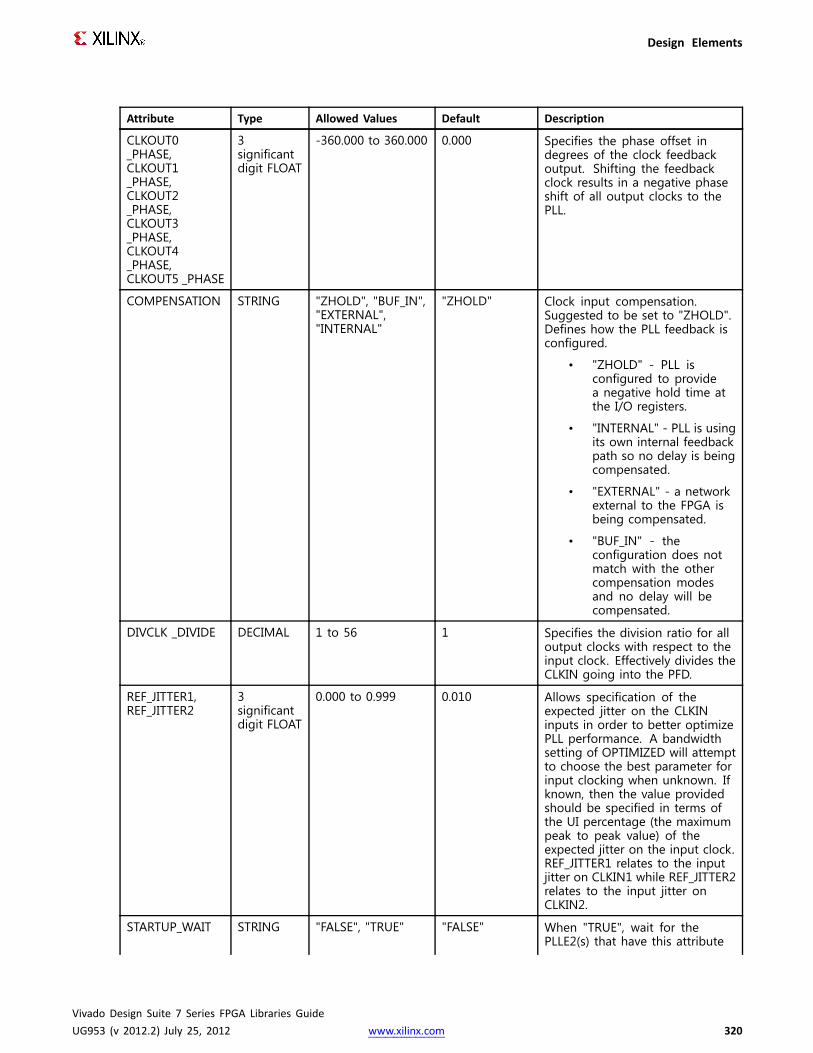
Design Elements
Attribute Type Allowed Values Default Description
CLKOUT0_PHASE,CLKOUT1_PHASE,CLKOUT2_PHASE,CLKOUT3_PHASE,CLKOUT4_PHASE,CLKOUT5 _PHASE
3significantdigit FLOAT
-360.000 to 360.000 0.000 Specifies the phase offset indegrees of the clock feedbackoutput. Shifting the feedbackclock results in a negative phaseshift of all output clocks to thePLL.
COMPENSATION STRING "ZHOLD", "BUF_IN","EXTERNAL","INTERNAL"
"ZHOLD" Clock input compensation.Suggested to be set to "ZHOLD".Defines how the PLL feedback isconfigured.
• "ZHOLD" - PLL isconfigured to providea negative hold time atthe I/O registers.
• "INTERNAL" - PLL is usingits own internal feedbackpath so no delay is beingcompensated.
• "EXTERNAL" - a networkexternal to the FPGA isbeing compensated.
• "BUF_IN" - theconfiguration does notmatch with the othercompensation modesand no delay will becompensated.
DIVCLK _DIVIDE DECIMAL 1 to 56 1 Specifies the division ratio for alloutput clocks with respect to theinput clock. Effectively divides theCLKIN going into the PFD.
REF_JITTER1,REF_JITTER2
3significantdigit FLOAT
0.000 to 0.999 0.010 Allows specification of theexpected jitter on the CLKINinputs in order to better optimizePLL performance. A bandwidthsetting of OPTIMIZED will attemptto choose the best parameter forinput clocking when unknown. Ifknown, then the value providedshould be specified in terms ofthe UI percentage (the maximumpeak to peak value) of theexpected jitter on the input clock.REF_JITTER1 relates to the inputjitter on CLKIN1 while REF_JITTER2relates to the input jitter onCLKIN2.
STARTUP_WAIT STRING "FALSE", "TRUE" "FALSE" When "TRUE", wait for thePLLE2(s) that have this attribute
Vivado Design Suite 7 Series FPGA Libraries GuideUG953 (v 2012.2) July 25, 2012 www.xilinx.com 320
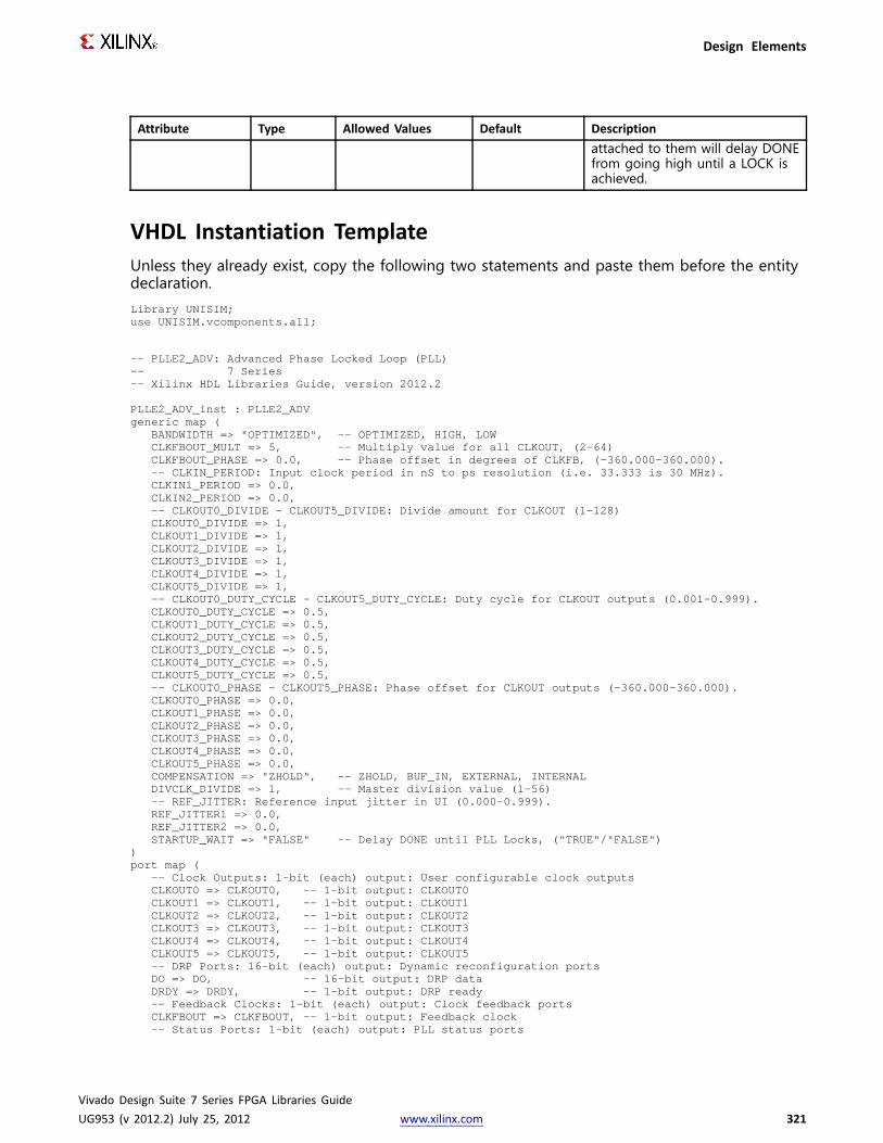
Design Elements
Attribute Type Allowed Values Default Descriptionattached to them will delay DONEfrom going high until a LOCK isachieved.
VHDL Instantiation TemplateUnless they already exist, copy the following two statements and paste them before the entitydeclaration.Library UNISIM;use UNISIM.vcomponents.all;
-- PLLE2_ADV: Advanced Phase Locked Loop (PLL)-- 7 Series-- Xilinx HDL Libraries Guide, version 2012.2
PLLE2_ADV_inst : PLLE2_ADVgeneric map (
BANDWIDTH=> "OPTIMIZED", -- OPTIMIZED, HIGH, LOWCLKFBOUT_MULT=> 5, -- Multiply value for all CLKOUT, (2-64)CLKFBOUT_PHASE=> 0.0, -- Phase offset in degrees of CLKFB, (-360.000-360.000).-- CLKIN_PERIOD: Input clock period in nS to ps resolution (i.e. 33.333 is 30 MHz).CLKIN1_PERIOD => 0.0,CLKIN2_PERIOD => 0.0,-- CLKOUT0_DIVIDE - CLKOUT5_DIVIDE: Divide amount for CLKOUT(1-128)CLKOUT0_DIVIDE => 1,CLKOUT1_DIVIDE => 1,CLKOUT2_DIVIDE => 1,CLKOUT3_DIVIDE => 1,CLKOUT4_DIVIDE => 1,CLKOUT5_DIVIDE => 1,-- CLKOUT0_DUTY_CYCLE- CLKOUT5_DUTY_CYCLE:Duty cycle for CLKOUToutputs (0.001-0.999).CLKOUT0_DUTY_CYCLE=> 0.5,CLKOUT1_DUTY_CYCLE=> 0.5,CLKOUT2_DUTY_CYCLE=> 0.5,CLKOUT3_DUTY_CYCLE=> 0.5,CLKOUT4_DUTY_CYCLE=> 0.5,CLKOUT5_DUTY_CYCLE=> 0.5,-- CLKOUT0_PHASE- CLKOUT5_PHASE:Phase offset for CLKOUToutputs (-360.000-360.000).CLKOUT0_PHASE=> 0.0,CLKOUT1_PHASE=> 0.0,CLKOUT2_PHASE=> 0.0,CLKOUT3_PHASE=> 0.0,CLKOUT4_PHASE=> 0.0,CLKOUT5_PHASE=> 0.0,COMPENSATION=> "ZHOLD", -- ZHOLD, BUF_IN, EXTERNAL, INTERNALDIVCLK_DIVIDE => 1, -- Master division value (1-56)-- REF_JITTER: Reference input jitter in UI (0.000-0.999).REF_JITTER1 => 0.0,REF_JITTER2 => 0.0,STARTUP_WAIT=> "FALSE" -- Delay DONEuntil PLL Locks, ("TRUE"/"FALSE")
)port map (
-- Clock Outputs: 1-bit (each) output: User configurable clock outputsCLKOUT0 => CLKOUT0, -- 1-bit output: CLKOUT0CLKOUT1 => CLKOUT1, -- 1-bit output: CLKOUT1CLKOUT2 => CLKOUT2, -- 1-bit output: CLKOUT2CLKOUT3 => CLKOUT3, -- 1-bit output: CLKOUT3CLKOUT4 => CLKOUT4, -- 1-bit output: CLKOUT4CLKOUT5 => CLKOUT5, -- 1-bit output: CLKOUT5-- DRP Ports: 16-bit (each) output: Dynamic reconfiguration portsDO => DO, -- 16-bit output: DRP dataDRDY=> DRDY, -- 1-bit output: DRP ready-- Feedback Clocks: 1-bit (each) output: Clock feedback portsCLKFBOUT=> CLKFBOUT, -- 1-bit output: Feedback clock-- Status Ports: 1-bit (each) output: PLL status ports
Vivado Design Suite 7 Series FPGA Libraries GuideUG953 (v 2012.2) July 25, 2012 www.xilinx.com 321

Design Elements
LOCKED=> LOCKED, -- 1-bit output: LOCK-- Clock Inputs: 1-bit (each) input: Clock inputsCLKIN1 => CLKIN1, -- 1-bit input: Primary clockCLKIN2 => CLKIN2, -- 1-bit input: Secondary clock-- Control Ports: 1-bit (each) input: PLL control portsCLKINSEL => CLKINSEL, -- 1-bit input: Clock select, High=CLKIN1 Low=CLKIN2PWRDWN=> PWRDWN, -- 1-bit input: Power-downRST => RST, -- 1-bit input: Reset-- DRP Ports: 7-bit (each) input: Dynamic reconfiguration portsDADDR=> DADDR, -- 7-bit input: DRP addressDCLK => DCLK, -- 1-bit input: DRP clockDEN => DEN, -- 1-bit input: DRP enableDI => DI, -- 16-bit input: DRP dataDWE=> DWE, -- 1-bit input: DRP write enable-- Feedback Clocks: 1-bit (each) input: Clock feedback portsCLKFBIN => CLKFBIN -- 1-bit input: Feedback clock
);
-- End of PLLE2_ADV_inst instantiation
Verilog Instantiation Template
// PLLE2_ADV: Advanced Phase Locked Loop (PLL)// 7 Series// Xilinx HDL Libraries Guide, version 2012.2
PLLE2_ADV #(.BANDWIDTH("OPTIMIZED"), // OPTIMIZED, HIGH, LOW.CLKFBOUT_MULT(5), // Multiply value for all CLKOUT, (2-64).CLKFBOUT_PHASE(0.0), // Phase offset in degrees of CLKFB, (-360.000-360.000).// CLKIN_PERIOD: Input clock period in nS to ps resolution (i.e. 33.333 is 30 MHz)..CLKIN1_PERIOD(0.0),.CLKIN2_PERIOD(0.0),// CLKOUT0_DIVIDE - CLKOUT5_DIVIDE: Divide amount for CLKOUT(1-128).CLKOUT0_DIVIDE(1),.CLKOUT1_DIVIDE(1),.CLKOUT2_DIVIDE(1),.CLKOUT3_DIVIDE(1),.CLKOUT4_DIVIDE(1),.CLKOUT5_DIVIDE(1),// CLKOUT0_DUTY_CYCLE- CLKOUT5_DUTY_CYCLE:Duty cycle for CLKOUToutputs (0.001-0.999)..CLKOUT0_DUTY_CYCLE(0.5),.CLKOUT1_DUTY_CYCLE(0.5),.CLKOUT2_DUTY_CYCLE(0.5),.CLKOUT3_DUTY_CYCLE(0.5),.CLKOUT4_DUTY_CYCLE(0.5),.CLKOUT5_DUTY_CYCLE(0.5),// CLKOUT0_PHASE- CLKOUT5_PHASE:Phase offset for CLKOUToutputs (-360.000-360.000)..CLKOUT0_PHASE(0.0),.CLKOUT1_PHASE(0.0),.CLKOUT2_PHASE(0.0),.CLKOUT3_PHASE(0.0),.CLKOUT4_PHASE(0.0),.CLKOUT5_PHASE(0.0),.COMPENSATION("ZHOLD"), // ZHOLD, BUF_IN, EXTERNAL, INTERNAL.DIVCLK_DIVIDE(1), // Master division value (1-56)// REF_JITTER: Reference input jitter in UI (0.000-0.999)..REF_JITTER1(0.0),.REF_JITTER2(0.0),.STARTUP_WAIT("FALSE") // Delay DONEuntil PLL Locks, ("TRUE"/"FALSE")
)PLLE2_ADV_inst (
// Clock Outputs: 1-bit (each) output: User configurable clock outputs.CLKOUT0(CLKOUT0), // 1-bit output: CLKOUT0.CLKOUT1(CLKOUT1), // 1-bit output: CLKOUT1.CLKOUT2(CLKOUT2), // 1-bit output: CLKOUT2.CLKOUT3(CLKOUT3), // 1-bit output: CLKOUT3.CLKOUT4(CLKOUT4), // 1-bit output: CLKOUT4.CLKOUT5(CLKOUT5), // 1-bit output: CLKOUT5// DRP Ports: 16-bit (each) output: Dynamic reconfiguration ports
Vivado Design Suite 7 Series FPGA Libraries GuideUG953 (v 2012.2) July 25, 2012 www.xilinx.com 322
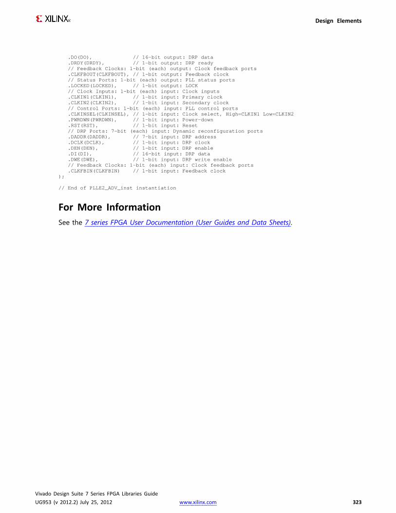
Design Elements
.DO(DO), // 16-bit output: DRP data
.DRDY(DRDY), // 1-bit output: DRP ready// Feedback Clocks: 1-bit (each) output: Clock feedback ports.CLKFBOUT(CLKFBOUT), // 1-bit output: Feedback clock// Status Ports: 1-bit (each) output: PLL status ports.LOCKED(LOCKED), // 1-bit output: LOCK// Clock Inputs: 1-bit (each) input: Clock inputs.CLKIN1(CLKIN1), // 1-bit input: Primary clock.CLKIN2(CLKIN2), // 1-bit input: Secondary clock// Control Ports: 1-bit (each) input: PLL control ports.CLKINSEL(CLKINSEL), // 1-bit input: Clock select, High=CLKIN1 Low=CLKIN2.PWRDWN(PWRDWN), // 1-bit input: Power-down.RST(RST), // 1-bit input: Reset// DRP Ports: 7-bit (each) input: Dynamic reconfiguration ports.DADDR(DADDR), // 7-bit input: DRP address.DCLK(DCLK), // 1-bit input: DRP clock.DEN(DEN), // 1-bit input: DRP enable.DI(DI), // 16-bit input: DRP data.DWE(DWE), // 1-bit input: DRP write enable// Feedback Clocks: 1-bit (each) input: Clock feedback ports.CLKFBIN(CLKFBIN) // 1-bit input: Feedback clock
);
// End of PLLE2_ADV_inst instantiation
For More InformationSee the 7 series FPGA User Documentation (User Guides and Data Sheets).
Vivado Design Suite 7 Series FPGA Libraries GuideUG953 (v 2012.2) July 25, 2012 www.xilinx.com 323

Design Elements
PLLE2_BASEPrimitive: Base Phase Locked Loop (PLL)
IntroductionThe PLLE2 is a mixed signal block designed to support frequency synthesis, clock networkdeskew, and jitter reduction. The clock outputs can each have an individual divide, phase shiftand duty cycle based on the same VCO frequency. The PLLE2 complements the MMCM bysupporting higher speed clocking while the MMCM has more features to handle most generalclocking needs. The PLLE2_BASE is intended for most uses of this PLL component while thePLLE2_ADV is intended for use when clock switch-over or dynamic reconfiguration is required.
Port DescriptionsPort Direction Width Function
CLKFBIN Input 1 Feedback clock pin to the PLL
CLKFBOUT Output 1 Dedicated PLL Feedback clock output
Clock Input Input 1 General clock input.
Clock Outpu ts Output 1 User configurable clock outputs that can bedivided versions of the VCO phase outputs(user controllable) from 1 (bypassed) to 128.The output clocks are phase aligned to eachother (unless phase shifted) and alignedto the input clock with a proper feedbackconfiguration. .
PWRDWN Input 1 Powers down instantiated but unused PLLs.
RST Input 1 The RST signal is an asynchronous reset forthe PLL. The PLL will synchronously re-enableitself when this signal is released and gothrough a new phase alignment and lock
Vivado Design Suite 7 Series FPGA Libraries GuideUG953 (v 2012.2) July 25, 2012 www.xilinx.com 324

Design Elements
Port Direction Width Functioncycle. A reset is required when the input clockconditions change (e.g., frequency).
Status Port Output 1 An output from the PLL that indicates whenthe PLL has achieved phase alignment withina predefined window and frequency matchingwithin a predefined PPM range. The PLLautomatically locks after power on, no extrareset is required. LOCKED will be deasserted ifthe input clock stops or the phase alignmentis violated (e.g., input clock phase shift).The PLL automatically reacquires lock afterLOCKED is deasserted.
Design Entry MethodInstantiation Yes
Inference No
CORE Generator™ and wizards Yes
Macro support No
Available AttributesAttribute Type Allowed Values Default Description
BANDWIDTH STRING "OPTIMIZED","HIGH", "LOW"
"OPTIMIZED" Specifies the PLLE2 programmingalgorithm affecting the jitter,phase margin and othercharacteristics of the PLLE2.
CLKFBOUT _MULT DECIMAL 2 to 64 5 Specifies the amount to multiplyall CLKOUT clock outputs if adifferent frequency is desired. Thisnumber, in combination with theassociated CLKOUT#_DIVIDE valueand DIVCLK_DIVIDE value, willdetermine the output frequency.
CLKFBOUT _PHASE 3significantdigitFLOAT
-360.000 to360.000
0.000 Specifies the phase offset indegrees of the clock feedbackoutput. Shifting the feedbackclock results in a negative phaseshift of all output clocks to thePLL.
CLKIN1 _PERIOD FLOAT(nS) 0.000 to 52.631 0.000 Specifies the input period in ns tothe PLL CLKIN1 input. Resolutionis down to the ps (3 decimalplaces). For exmaple a value of33.333 would indicate a 30 MHzinput clock. This information ismandatory and must be supplied.
Vivado Design Suite 7 Series FPGA Libraries GuideUG953 (v 2012.2) July 25, 2012 www.xilinx.com 325
Design Elements
Attribute Type Allowed Values Default Description
CLKOUT0 _DIVIDE,CLKOUT1 _DIVIDE,CLKOUT2 _DIVIDE,CLKOUT3 _DIVIDE,CLKOUT4 _DIVIDE,CLKOUT5 _DIVIDE
DECIMAL 1 to 128 1 Specifies the amount to divide theassociated CLKOUT clock outputif a different frequency is desired.This number in combinationwith the CLKFBOUT_MULTand DIVCLK_DIVIDE values willdetermine the output frequency.
CLKOUT0_DUTY_CYCLE,CLKOUT1_DUTY_CYCLE,CLKOUT2_DUTY_CYCLE,CLKOUT3_DUTY_CYCLE,CLKOUT4_DUTY_CYCLE,CLKOUT5_DUTY_CYCLE
3significantdigitFLOAT
0.001 to 0.999 0.500 Specifies the Duty Cycle of theassociated CLKOUT clock outputin percentage (i.e., 0.500 willgenerate a 50% duty cycle).
CLKOUT0 _PHASE,CLKOUT1 _PHASE,CLKOUT2 _PHASE,CLKOUT3 _PHASE,CLKOUT4 _PHASE,CLKOUT5 _PHASE
3significantdigitFLOAT
-360.000 to360.000
0.000 Specifies the phase offset indegrees of the clock feedbackoutput. Shifting the feedbackclock results in a negative phaseshift of all output clocks to thePLL.
DIVCLK _DIVIDE DECIMAL 1 to 56 1 Specifies the division ratio for alloutput clocks with respect to theinput clock. Effectively divides theCLKIN going into the PFD.
REF_JITTER1 3significantdigitFLOAT
0.000 to 0.999 0.010 Allows specification of theexpected jitter on CLKIN1 inorder to better optimize PLLperformance. A bandwidthsetting of OPTIMIZED will attemptto choose the best parameter forinput clocking when unknown. Ifknown, then the value providedshould be specified in terms of theUI percentage (the maximum peakto peak value) of the expectedjitter on the input clock.
STARTUP_WAIT STRING "FALSE", "TRUE" "FALSE" When "TRUE", wait for thePLLE2(s) that have this attributeattached to them will delay DONEfrom going high until a LOCK isachieved.
Vivado Design Suite 7 Series FPGA Libraries GuideUG953 (v 2012.2) July 25, 2012 www.xilinx.com 326

Design Elements
VHDL Instantiation TemplateUnless they already exist, copy the following two statements and paste them before the entitydeclaration.Library UNISIM;use UNISIM.vcomponents.all;
-- PLLE2_BASE: Base Phase Locked Loop (PLL)-- 7 Series-- Xilinx HDL Libraries Guide, version 2012.2
PLLE2_BASE_inst : PLLE2_BASEgeneric map (
BANDWIDTH=> "OPTIMIZED", -- OPTIMIZED, HIGH, LOWCLKFBOUT_MULT=> 5, -- Multiply value for all CLKOUT, (2-64)CLKFBOUT_PHASE=> 0.0, -- Phase offset in degrees of CLKFB, (-360.000-360.000).CLKIN1_PERIOD => 0.0, -- Input clock period in ns to ps resolution (i.e. 33.333 is 30 MHz).-- CLKOUT0_DIVIDE - CLKOUT5_DIVIDE: Divide amount for each CLKOUT(1-128)CLKOUT0_DIVIDE => 1,CLKOUT1_DIVIDE => 1,CLKOUT2_DIVIDE => 1,CLKOUT3_DIVIDE => 1,CLKOUT4_DIVIDE => 1,CLKOUT5_DIVIDE => 1,-- CLKOUT0_DUTY_CYCLE- CLKOUT5_DUTY_CYCLE:Duty cycle for each CLKOUT(0.001-0.999).CLKOUT0_DUTY_CYCLE=> 0.5,CLKOUT1_DUTY_CYCLE=> 0.5,CLKOUT2_DUTY_CYCLE=> 0.5,CLKOUT3_DUTY_CYCLE=> 0.5,CLKOUT4_DUTY_CYCLE=> 0.5,CLKOUT5_DUTY_CYCLE=> 0.5,-- CLKOUT0_PHASE- CLKOUT5_PHASE:Phase offset for each CLKOUT(-360.000-360.000).CLKOUT0_PHASE=> 0.0,CLKOUT1_PHASE=> 0.0,CLKOUT2_PHASE=> 0.0,CLKOUT3_PHASE=> 0.0,CLKOUT4_PHASE=> 0.0,CLKOUT5_PHASE=> 0.0,DIVCLK_DIVIDE => 1, -- Master division value, (1-56)REF_JITTER1 => 0.0, -- Reference input jitter in UI, (0.000-0.999).STARTUP_WAIT=> "FALSE" -- Delay DONEuntil PLL Locks, ("TRUE"/"FALSE")
)port map (
-- Clock Outputs: 1-bit (each) output: User configurable clock outputsCLKOUT0 => CLKOUT0,CLKOUT1 => CLKOUT1,CLKOUT2 => CLKOUT2,CLKOUT3 => CLKOUT3,CLKOUT4 => CLKOUT4,CLKOUT5 => CLKOUT5,-- Feedback Clocks: 1-bit (each) output: Clock feedback portsCLKFBOUT=> CLKFBOUT, -- 1-bit output: Feedback clock-- Status Port: 1-bit (each) output: PLL status portsLOCKED=> LOCKED, -- 1-bit output: LOCK-- Clock Input: 1-bit (each) input: Clock inputCLKIN1 => CLKIN1, -- 1-bit input: Input clock-- Control Ports: 1-bit (each) input: PLL control portsPWRDWN=> PWRDWN, -- 1-bit input: Power-downRST => RST, -- 1-bit input: Reset-- Feedback Clocks: 1-bit (each) input: Clock feedback portsCLKFBIN => CLKFBIN -- 1-bit input: Feedback clock
);
-- End of PLLE2_BASE_inst instantiation
Vivado Design Suite 7 Series FPGA Libraries GuideUG953 (v 2012.2) July 25, 2012 www.xilinx.com 327

Design Elements
Verilog Instantiation Template
// PLLE2_BASE: Base Phase Locked Loop (PLL)// 7 Series// Xilinx HDL Libraries Guide, version 2012.2
PLLE2_BASE #(.BANDWIDTH("OPTIMIZED"), // OPTIMIZED, HIGH, LOW.CLKFBOUT_MULT(5), // Multiply value for all CLKOUT, (2-64).CLKFBOUT_PHASE(0.0), // Phase offset in degrees of CLKFB, (-360.000-360.000)..CLKIN1_PERIOD(0.0), // Input clock period in ns to ps resolution (i.e. 33.333 is 30 MHz).// CLKOUT0_DIVIDE - CLKOUT5_DIVIDE: Divide amount for each CLKOUT(1-128).CLKOUT0_DIVIDE(1),.CLKOUT1_DIVIDE(1),.CLKOUT2_DIVIDE(1),.CLKOUT3_DIVIDE(1),.CLKOUT4_DIVIDE(1),.CLKOUT5_DIVIDE(1),// CLKOUT0_DUTY_CYCLE- CLKOUT5_DUTY_CYCLE:Duty cycle for each CLKOUT(0.001-0.999)..CLKOUT0_DUTY_CYCLE(0.5),.CLKOUT1_DUTY_CYCLE(0.5),.CLKOUT2_DUTY_CYCLE(0.5),.CLKOUT3_DUTY_CYCLE(0.5),.CLKOUT4_DUTY_CYCLE(0.5),.CLKOUT5_DUTY_CYCLE(0.5),// CLKOUT0_PHASE- CLKOUT5_PHASE:Phase offset for each CLKOUT(-360.000-360.000)..CLKOUT0_PHASE(0.0),.CLKOUT1_PHASE(0.0),.CLKOUT2_PHASE(0.0),.CLKOUT3_PHASE(0.0),.CLKOUT4_PHASE(0.0),.CLKOUT5_PHASE(0.0),.DIVCLK_DIVIDE(1), // Master division value, (1-56).REF_JITTER1(0.0), // Reference input jitter in UI, (0.000-0.999)..STARTUP_WAIT("FALSE") // Delay DONEuntil PLL Locks, ("TRUE"/"FALSE")
)PLLE2_BASE_inst (
// Clock Outputs: 1-bit (each) output: User configurable clock outputs.CLKOUT0(CLKOUT0),.CLKOUT1(CLKOUT1),.CLKOUT2(CLKOUT2),.CLKOUT3(CLKOUT3),.CLKOUT4(CLKOUT4),.CLKOUT5(CLKOUT5),// Feedback Clocks: 1-bit (each) output: Clock feedback ports.CLKFBOUT(CLKFBOUT), // 1-bit output: Feedback clock// Status Port: 1-bit (each) output: PLL status ports.LOCKED(LOCKED), // 1-bit output: LOCK// Clock Input: 1-bit (each) input: Clock input.CLKIN1(CLKIN1), // 1-bit input: Input clock// Control Ports: 1-bit (each) input: PLL control ports.PWRDWN(PWRDWN), // 1-bit input: Power-down.RST(RST), // 1-bit input: Reset// Feedback Clocks: 1-bit (each) input: Clock feedback ports.CLKFBIN(CLKFBIN) // 1-bit input: Feedback clock
);
// End of PLLE2_BASE_inst instantiation
For More InformationSee the 7 series FPGA User Documentation (User Guides and Data Sheets).
Vivado Design Suite 7 Series FPGA Libraries GuideUG953 (v 2012.2) July 25, 2012 www.xilinx.com 328
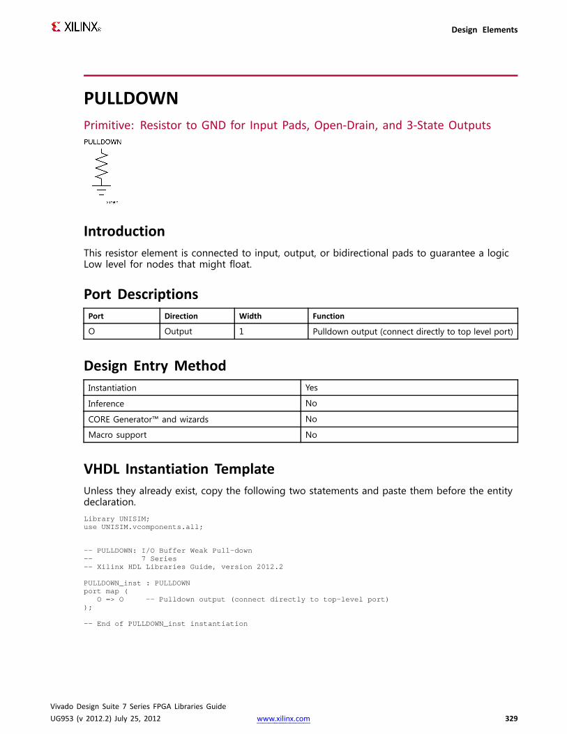
Design Elements
PULLDOWNPrimitive: Resistor to GND for Input Pads, Open-Drain, and 3-State Outputs
IntroductionThis resistor element is connected to input, output, or bidirectional pads to guarantee a logicLow level for nodes that might float.
Port DescriptionsPort Direction Width Function
O Output 1 Pulldown output (connect directly to top level port)
Design Entry MethodInstantiation Yes
Inference No
CORE Generator™ and wizards No
Macro support No
VHDL Instantiation TemplateUnless they already exist, copy the following two statements and paste them before the entitydeclaration.Library UNISIM;use UNISIM.vcomponents.all;
-- PULLDOWN:I/O Buffer Weak Pull-down-- 7 Series-- Xilinx HDL Libraries Guide, version 2012.2
PULLDOWN_inst : PULLDOWNport map (
O => O -- Pulldown output (connect directly to top-level port));
-- End of PULLDOWN_inst instantiation
Vivado Design Suite 7 Series FPGA Libraries GuideUG953 (v 2012.2) July 25, 2012 www.xilinx.com 329

Design Elements
Verilog Instantiation Template
// PULLDOWN:I/O Buffer Weak Pull-down// 7 Series// Xilinx HDL Libraries Guide, version 2012.2
PULLDOWNPULLDOWN_inst (.O(O) // Pulldown output (connect directly to top-level port)
);
// End of PULLDOWN_inst instantiation
For More InformationSee the 7 series FPGA User Documentation (User Guides and Data Sheets).
Vivado Design Suite 7 Series FPGA Libraries GuideUG953 (v 2012.2) July 25, 2012 www.xilinx.com 330

Design Elements
PULLUPPrimitive: Resistor to VCC for Input PADs, Open-Drain, and 3-State Outputs
IntroductionThis design element allows for an input, 3-state output or bi-directional port to be driven toa weak high value when not being driven by an internal or external source. This elementestablishes a High logic level for open-drain elements and macros when all the drivers are off.
Port DescriptionsPort Direction Width Function
O Output 1 Pullup output (connect directly to top level port)
Design Entry MethodInstantiation Yes
Inference No
CORE Generator™ and wizards No
Macro support No
VHDL Instantiation TemplateUnless they already exist, copy the following two statements and paste them before the entitydeclaration.Library UNISIM;use UNISIM.vcomponents.all;
-- PULLUP: I/O Buffer Weak Pull-up-- 7 Series-- Xilinx HDL Libraries Guide, version 2012.2
PULLUP_inst : PULLUPport map (
O => O -- Pullup output (connect directly to top-level port));
-- End of PULLUP_inst instantiation
Vivado Design Suite 7 Series FPGA Libraries GuideUG953 (v 2012.2) July 25, 2012 www.xilinx.com 331

Design Elements
Verilog Instantiation Template
// PULLUP: I/O Buffer Weak Pull-up// 7 Series// Xilinx HDL Libraries Guide, version 2012.2
PULLUP PULLUP_inst (.O(O) // Pullup output (connect directly to top-level port)
);
// End of PULLUP_inst instantiation
For More InformationSee the 7 series FPGA User Documentation (User Guides and Data Sheets).
Vivado Design Suite 7 Series FPGA Libraries GuideUG953 (v 2012.2) July 25, 2012 www.xilinx.com 332

Design Elements
RAM128X1DPrimitive: 128-Deep by 1-Wide Dual Port Random Access Memory (Select RAM)
IntroductionThis design element is a 128-bit deep by 1-bit wide random access memory and has aread/write port that writes the value on the D input data pin when the write enable (WE) ishigh to the location specified by the A address bus. This happens shortly after the risingedge of the WCLK and that same value is reflected in the data output SPO. When WE is low,an asynchronous read is initiated in which the contents of the memory location specified bythe A address bus is output asynchronously to the SPO output. The read port can performasynchronous read access of the memory by changing the value of the address bus DPRA, andby outputing that value to the DPO data output.
Port DescriptionsPort Direction Width Function
SPO Output 1 Read/Write port data output addressed by A
DPO Output 1 Read port data output addressed by DPRA
D Input 1 Write data input addressed by A
A Input 7 Read/Write port address bus
DPRA Input 7 Read port address bus
WE Input 1 Write Enable
WCLK Input 1 Write clock (reads are asynchronous)
Vivado Design Suite 7 Series FPGA Libraries GuideUG953 (v 2012.2) July 25, 2012 www.xilinx.com 333

Design Elements
If instantiated, the following connections should be made to this component:• Tie the WCLK input to the desired clock source, the D input to the data source to be
stored and the DPO output to an FDCE D input or other appropriate data destination.• Optionally, the SPO output can also be connected to the appropriate data destination
or else left unconnected.• The WE clock enable pin should be connected to the proper write enable source
in the design.• The 7-bit A bus should be connected to the source for the read/write addressing and
the 7-bit DPRA bus should be connected to the appropriate read address connections.• An optional INIT attribute consisting of a 128-bit Hexadecimal value can be specified to
indicate the initial contents of the RAM.
If left unspecified, the initial contents default to all zeros.
Design Entry MethodInstantiation Yes
Inference Recommended
CORE Generator™ and wizards No
Macro support No
Available AttributesAttribute Type Allowed Values Default Description
INIT Hexadecimal Any 128-Bit Value All zeros Specifies the initial contents of theRAM.
VHDL Instantiation TemplateUnless they already exist, copy the following two statements and paste them before the entitydeclaration.Library UNISIM;use UNISIM.vcomponents.all;
-- RAM128X1D: 128-deep by 1-wide positive edge write, asynchronous read-- dual-port distributed LUT RAM (Mapped to two SliceM LUT6s)-- 7 Series-- Xilinx HDL Libraries Guide, version 2012.2
RAM128X1D_inst : RAM128X1Dgeneric map (
INIT => X"00000000000000000000000000000000")port map (
DPO => DPO, -- Read/Write port 1-bit outputSPO => SPO, -- Read port 1-bit outputA => A, -- Read/Write port 7-bit address inputD => D, -- RAMdata inputDPRA => DPRA, -- Read port 7-bit address inputWCLK=> WCLK, -- Write clock inputWE => WE -- RAMdata input
);
Vivado Design Suite 7 Series FPGA Libraries GuideUG953 (v 2012.2) July 25, 2012 www.xilinx.com 334

Design Elements
-- End of RAM128X1D_inst instantiation
Verilog Instantiation Template
// RAM128X1D: 128-deep by 1-wide positive edge write, asynchronous read (Mapped to two SliceM LUT6s)// dual-port distributed LUT RAM// 7 Series// Xilinx HDL Libraries Guide, version 2012.2
RAM128X1D#(.INIT(128'h00000000000000000000000000000000)
) RAM128X1D_inst (.DPO(DPO), // Read port 1-bit output.SPO(SPO), // Readw/rite port 1-bit output.A(A), // Readw/rite port 7-bit address input.D(D), // RAMdata input.DPRA(DPRA), // Read port 7-bit address input.WCLK(WCLK), // Write clock input.WE(WE) // Write enable input
);
// End of RAM128X1D_inst instantiation
For More InformationSee the 7 series FPGA User Documentation (User Guides and Data Sheets).
Vivado Design Suite 7 Series FPGA Libraries GuideUG953 (v 2012.2) July 25, 2012 www.xilinx.com 335
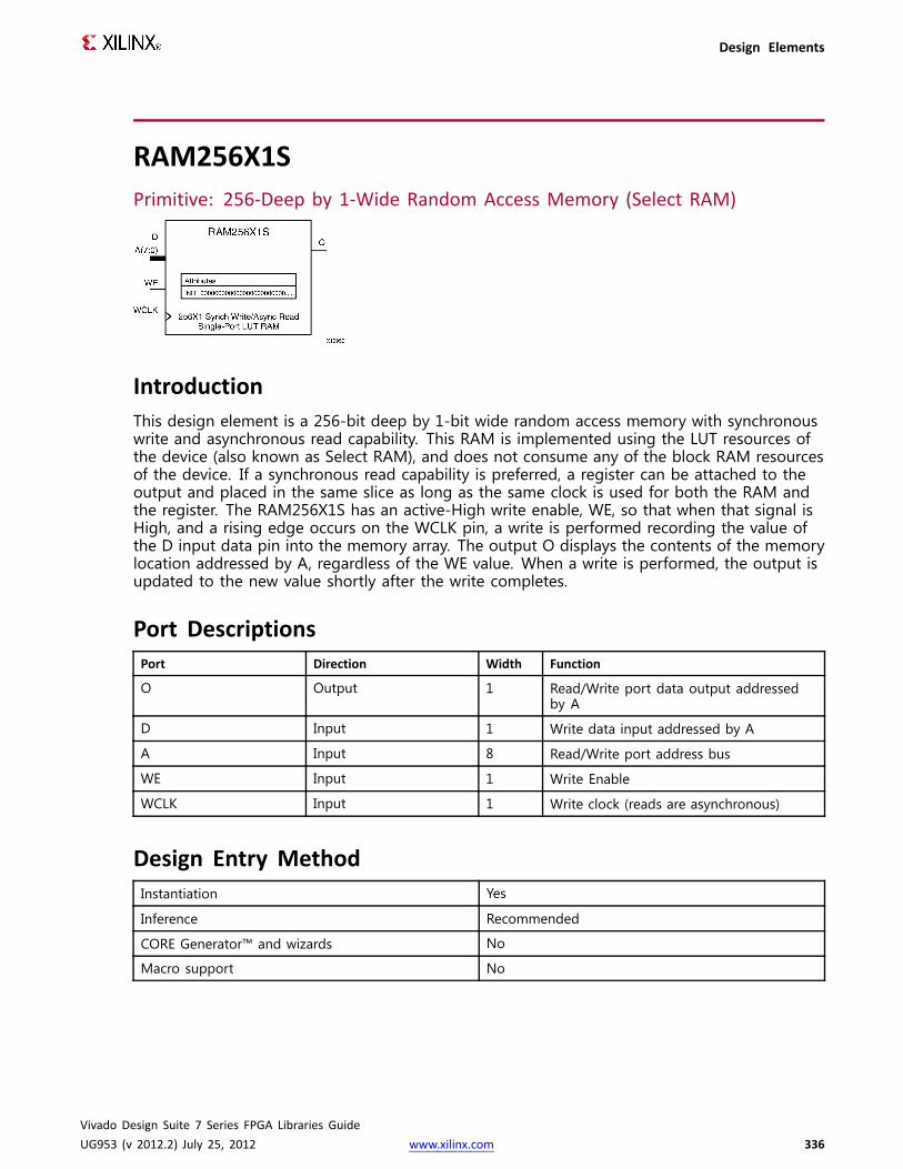
Design Elements
RAM256X1SPrimitive: 256-Deep by 1-Wide Random Access Memory (Select RAM)
IntroductionThis design element is a 256-bit deep by 1-bit wide random access memory with synchronouswrite and asynchronous read capability. This RAM is implemented using the LUT resources ofthe device (also known as Select RAM), and does not consume any of the block RAM resourcesof the device. If a synchronous read capability is preferred, a register can be attached to theoutput and placed in the same slice as long as the same clock is used for both the RAM andthe register. The RAM256X1S has an active-High write enable, WE, so that when that signal isHigh, and a rising edge occurs on the WCLK pin, a write is performed recording the value ofthe D input data pin into the memory array. The output O displays the contents of the memorylocation addressed by A, regardless of the WE value. When a write is performed, the output isupdated to the new value shortly after the write completes.
Port DescriptionsPort Direction Width Function
O Output 1 Read/Write port data output addressedby A
D Input 1 Write data input addressed by A
A Input 8 Read/Write port address bus
WE Input 1 Write Enable
WCLK Input 1 Write clock (reads are asynchronous)
Design Entry MethodInstantiation Yes
Inference Recommended
CORE Generator™ and wizards No
Macro support No
Vivado Design Suite 7 Series FPGA Libraries GuideUG953 (v 2012.2) July 25, 2012 www.xilinx.com 336
Design Elements
If instantiated, the following connections should be made to this component:
• Tie the WCLK input to the desired clock source, the D input to the data source to bestored, and the O output to an FDCE D input or other appropriate data destination.
• The WE clock enable pin should be connected to the proper write enable sourcein the design.
• The 8-bit A bus should be connected to the source for the read/write.
• An optional INIT attribute consisting of a 256-bit Hexadecimal value can be specified toindicate the initial contents of the RAM.
If left unspecified, the initial contents default to all zeros.
Available AttributesAttribute Data Type Allowed Values Default Description
INIT Hexadecimal Any 256-Bit Value Allzeros
Specifies the initial contents of the RAM.
VHDL Instantiation TemplateUnless they already exist, copy the following two statements and paste them before the entitydeclaration.Library UNISIM;use UNISIM.vcomponents.all;
-- RAM256X1S: 256-deep by 1-wide positive edge write, asynchronous read-- single-port distributed LUT RAM (Mapped to four SliceM LUT6s)-- 7 Series-- Xilinx HDL Libraries Guide, version 2012.2
RAM256X1S_inst : RAM256X1Sgeneric map (
INIT => X"0000000000000000000000000000000000000000000000000000000000000000")port map (
O => O, -- Read/Write port 1-bit outputA => A, -- Read/Write port 8-bit address inputD => D, -- RAMdata inputWCLK=> WCLK, -- Write clock inputWE => WE -- Write enable input
);
-- End of RAM256X1S_inst instantiation
Vivado Design Suite 7 Series FPGA Libraries GuideUG953 (v 2012.2) July 25, 2012 www.xilinx.com 337

Design Elements
Verilog Instantiation Template
// RAM256X1S: 256-deep by 1-wide positive edge write, asynchronous read (Mapped to forur SliceM LUT6s)// single-port distributed LUT RAM// 7 Series// Xilinx HDL Libraries Guide, version 2012.2
RAM256X1S #(.INIT(256'h0000000000000000000000000000000000000000000000000000000000000000)
) RAM256X1S_inst (.O(O), // Readw/rite port 1-bit output.A(A), // Readw/rite port 8-bit address input.WE(WE), // Write enable input.WCLK(WCLK), // Write clock input.D(D) // RAMdata input
);
// End of RAM256X1S_inst instantiation
For More InformationSee the 7 series FPGA User Documentation (User Guides and Data Sheets).
Vivado Design Suite 7 Series FPGA Libraries GuideUG953 (v 2012.2) July 25, 2012 www.xilinx.com 338

Design Elements
RAM32MPrimitive: 32-Deep by 8-bit Wide Multi Port Random Access Memory (SelectRAM)
IntroductionThis design element is a 32-bit deep by 8-bit wide, multi-port, random access memory withsynchronous write and asynchronous independent, 2-bit, wide-read capability. This RAM isimplemented using the LUT resources of the device known as SelectRAM™, and does notconsume any of the Block RAM resources of the device. The RAM32M is implemented in a singleslice and consists of one 8-bit write, 2-bit read port and three separate 2-bit read ports fromthe same memory, which allows for byte-wide write and independent 2-bit read access RAM.
• If the DIA, DIB, DIC, and DID inputs are all tied to the same data inputs, the RAM canbecome a 1 read/write port, 3 independent read port, 32x2 quad port memory.
• If DID is grounded, DOD is not used.
• If ADDRA, ADDRB, and ADDRC are tied to the same address, the RAM becomes a 32x6simple dual port RAM.
• If ADDRD is tied to ADDRA, ADDRB, and ADDRC, then the RAM is a 32x8 single portRAM.
There are several other possible configurations for this RAM.
Vivado Design Suite 7 Series FPGA Libraries GuideUG953 (v 2012.2) July 25, 2012 www.xilinx.com 339

Design Elements
Port DescriptionsPort Direction Width Function
DOA Output 2 Read port data outputs addressed by ADDRA
DOB Output 2 Read port data outputs addressed by ADDRB
DOC Output 2 Read port data outputs addressed by ADDRC
DOD Output 2 Read/Write port data outputs addressed by ADDRD
DIA Input 2 Write data inputs addressed by ADDRD (read outputis addressed by ADDRA)
DIB Input 2 Write data inputs addressed by ADDRD (read outputis addressed by ADDRB)
DIC Input 2 Write data inputs addressed by ADDRD (read outputis addressed by ADDRC)
DID Input 2 Write data inputs addressed by ADDRD
ADDRA Input 5 Read address bus A
ADDRB Input 5 Read address bus B
ADDRC Input 5 Read address bus C
ADDRD Input 5 8-bit data write port, 2-bit data read port addressbus D
WE Input 1 Write Enable
WCLK Input 1 Write clock (reads are asynchronous)
Design Entry MethodInstantiation Yes
Inference Recommended
CORE Generator™ and wizards No
Macro support No
This element can be inferred by some synthesis tools by describing a RAM with a synchronouswrite and asynchronous read capability. Consult your synthesis tool documentation for detailson RAM inference capabilities and coding examples. You should instantiate this component ifyou have a need to implicitly specify the RAM function, or if you need to manually place orrelationally place the component. If a synchronous read capability is desired, the outputs canbe connected to an FDRSE (FDCPE if asynchronous reset is needed) in order to improve theoutput timing of the function. However, this is not necessary for the proper operation of theRAM. If you want to have the data clocked on the negative edge of a clock, an inverter can bedescribed on the clock input to this component. This inverter will be absorbed into the blockgiving the ability to write to the RAM on falling clock edges.
Vivado Design Suite 7 Series FPGA Libraries GuideUG953 (v 2012.2) July 25, 2012 www.xilinx.com 340

Design Elements
If instantiated, the following connections should be made to this component:• Connect the WCLK input to the desired clock source, the DIA, DIB, DIC• Connect the DIA, DIB, DIC, and DID inputs to the data source to be stored• Connect the DOA, DOB, DOC, and DOD outputs to an FDCE D input or other appropriate
data destination, or leave unconnected if not used• Connect the WE clock enable pin to the proper write enable source in the design• Connect the ADDRD bus to the source for the read/write addressing• Connect the ADDRA, ADDRB, and ADDRC buses to the appropriate read address
connections
The optional INIT_A, INIT_B, INIT_C and INIT_D attributes let you specify the initial memorycontents of each port using a 64-bit hexadecimal value. The INIT value correlates to the RAMaddressing by the following equation: ADDRy[z] = INIT_y[2*z+1:2*z]. For instance, if the RAMADDRC port is addressed to 00001, then the INIT_C[3:2] values would be the initial valuesshown on the DOC port before the first write occurs at that address. If left unspecified, theinitial contents will be all zeros.
Available AttributesAttribute Data Type Allowed Values Default Description
INIT_A Hexadecimal Any 64-Bit Value All zeros Specifies the initial contents of the RAMon port A.
INIT_B Hexadecimal Any 64-Bit Value All zeros Specifies the initial contents of the RAMon port B.
INIT_C Hexadecimal Any 64-Bit Value All zeros Specifies the initial contents of the RAMon port C.
INIT_D Hexadecimal Any 64-Bit Value All zeros Specifies the initial contents of the RAMon port D.
VHDL Instantiation TemplateUnless they already exist, copy the following two statements and paste them before the entitydeclaration.Library UNISIM;use UNISIM.vcomponents.all;
-- RAM32M: 32-deep by 8-wide Multi Port LUT RAM (Mapped to four SliceM LUT6s)-- 7 Series-- Xilinx HDL Libraries Guide, version 2012.2
RAM32M_inst : RAM32Mgeneric map (
INIT_A => X"0000000000000000", -- Initial contents of A portINIT_B => X"0000000000000000", -- Initial contents of B portINIT_C => X"0000000000000000", -- Initial contents of C portINIT_D => X"0000000000000000) -- Initial contents of D port
port map (DOA => DOA, -- Read port A 2-bit outputDOB => DOB, -- Read port B 2-bit outputDOC=> DOC, -- Read port C 2-bit outputDOD=> DOD, -- Read/Write port D 2-bit outputADDRA=> ADDRA, -- Read port A 5-bit address inputADDRB=> ADDRB, -- Read port B 5-bit address input
Vivado Design Suite 7 Series FPGA Libraries GuideUG953 (v 2012.2) July 25, 2012 www.xilinx.com 341

Design Elements
ADDRC=> ADDRC, -- Read port C 5-bit address inputADDRD=> ADDRD, -- Read/Write port D 5-bit address inputDIA => DIA, -- RAM2-bit data write input addressed by ADDRD,
-- read addressed by ADDRADIB => DIB, -- RAM2-bit data write input addressed by ADDRD,
-- read addressed by ADDRBDIC => DIC, -- RAM2-bit data write input addressed by ADDRD,
-- read addressed by ADDRCDID => DID, -- RAM2-bit data write input addressed by ADDRD,
-- read addressed by ADDRDWCLK=> WCLK, -- Write clock inputWE => WE -- Write enable input
);-- End of RAM32M_inst instantiation
Verilog Instantiation Template
// RAM32M: 32-deep by 8-wide Multi Port LUT RAM (Mapped to forur SliceM LUT6s)// 7 Series// Xilinx HDL Libraries Guide, version 2012.2
RAM32M#(.INIT_A(64'h0000000000000000), // Initial contents of A Port.INIT_B(64'h0000000000000000), // Initial contents of B Port.INIT_C(64'h0000000000000000), // Initial contents of C Port.INIT_D(64'h0000000000000000) // Initial contents of D Port
) RAM32M_inst (.DOA(DOA), // Read port A 2-bit output.DOB(DOB), // Read port B 2-bit output.DOC(DOC), // Read port C 2-bit output.DOD(DOD), // Readw/rite port D 2-bit output.ADDRA(ADDRA), // Read port A 5-bit address input.ADDRB(ADDRB), // Read port B 5-bit address input.ADDRC(ADDRC), // Read port C 5-bit address input.ADDRD(ADDRD), // Readw/rite port D 5-bit address input.DIA(DIA), // RAM2-bit data write input addressed by ADDRD,
// read addressed by ADDRA.DIB(DIB), // RAM2-bit data write input addressed by ADDRD,
// read addressed by ADDRB.DIC(DIC), // RAM2-bit data write input addressed by ADDRD,
// read addressed by ADDRC.DID(DID), // RAM2-bit data write input addressed by ADDRD,
// read addressed by ADDRD.WCLK(WCLK), // Write clock input.WE(WE) // Write enable input
);
// End of RAM32M_inst instantiation
For More InformationSee the 7 series FPGA User Documentation (User Guides and Data Sheets).
Vivado Design Suite 7 Series FPGA Libraries GuideUG953 (v 2012.2) July 25, 2012 www.xilinx.com 342

Design Elements
RAM32X1DPrimitive: 32-Deep by 1-Wide Static Dual Port Synchronous RAM
IntroductionThe design element is a 32-word by 1-bit static dual port random access memory withsynchronous write capability. The device has two separate address ports: the read address(DPRA4:DPRA0) and the write address (A4:A0). These two address ports are completelyasynchronous. The read address controls the location of the data driven out of the output pin(DPO), and the write address controls the destination of a valid write transaction. When the writeenable (WE) is Low, transitions on the write clock (WCLK) are ignored and data stored in theRAM is not affected. When WE is High, any positive transition on WCLK loads the data on thedata input (D) into the word selected by the 5-bit write address. For predictable performance,write address and data inputs must be stable before a Low-to-High WCLK transition. This RAMblock assumes an active-High WCLK. WCLK can be active-High or active-Low. Any inverterplaced on the WCLK input net is absorbed into the block. You can initialize RAM32X1D duringconfiguration using the INIT attribute. Mode selection is shown in the following logic table.
The SPO output reflects the data in the memory cell addressed by A4:A0. The DPO outputreflects the data in the memory cell addressed by DPRA4:DPRA0. The write process is notaffected by the address on the read address port.
Logic TableInputs Outputs
WE (Mode) WCLK D SPO DPO
0 (read) X X data_a data_d
1 (read) 0 X data_a data_d
1 (read) 1 X data_a data_d
1 (write) ↑ D D data_d
1 (read) ↓ X data_a data_d
Vivado Design Suite 7 Series FPGA Libraries GuideUG953 (v 2012.2) July 25, 2012 www.xilinx.com 343

Design Elements
Design Entry MethodInstantiation Yes
Inference Recommended
CORE Generator™ and wizards No
Macro support No
Available Attributes
Attribute Data TypeAllowedValues Default Descriptions
INIT Hexadecimal Any 32-BitValue
All Zeros Initializes ROMs, RAMs, registers, andlook-up tables.
VHDL Instantiation TemplateUnless they already exist, copy the following two statements and paste them before the entitydeclaration.Library UNISIM;use UNISIM.vcomponents.all;
-- RAM32X1D: 32 x 1 positive edge write, asynchronous read-- dual-port distributed RAM (Mapped to SliceM LUT6)-- 7 Series-- Xilinx HDL Libraries Guide, version 2012.2
RAM32X1D_inst : RAM32X1Dgeneric map (
INIT => X"00000000") -- Initial contents of RAMport map (
DPO => DPO, -- Read-only 1-bit data outputSPO => SPO, -- R/W 1-bit data outputA0 => A0, -- R/W address[0] input bitA1 => A1, -- R/W address[1] input bitA2 => A2, -- R/W address[2] input bitA3 => A3, -- R/W address[3] input bitA4 => A4, -- R/W address[4] input bitD => D, -- Write 1-bit data inputDPRA0 => DPRA0, -- Read-only address[0] input bitDPRA1 => DPRA1, -- Read-only address[1] input bitDPRA2 => DPRA2, -- Read-only address[2] input bitDPRA3 => DPRA3, -- Read-only address[3] input bitDPRA4 => DPRA4, -- Read-only address[4] input bitWCLK=> WCLK, -- Write clock inputWE => WE -- Write enable input
);
-- End of RAM32X1D_inst instantiation
Vivado Design Suite 7 Series FPGA Libraries GuideUG953 (v 2012.2) July 25, 2012 www.xilinx.com 344

Design Elements
Verilog Instantiation Template
// RAM32X1D: 32 x 1 positive edge write, asynchronous read dual-port distributed RAM (Mapped to a SliceM LUT6)// 7 Series// Xilinx HDL Libraries Guide, version 2012.2
RAM32X1D#(.INIT(32'h00000000) // Initial contents of RAM
) RAM32X1D_inst (.DPO(DPO), // Read-only 1-bit data output.SPO(SPO), // Rw/ 1-bit data output.A0(A0), // Rw/ address[0] input bit.A1(A1), // Rw/ address[1] input bit.A2(A2), // Rw/ address[2] input bit.A3(A3), // Rw/ address[3] input bit.A4(A4), // Rw/ address[4] input bit.D(D), // Write 1-bit data input.DPRA0(DPRA0), // Read-only address[0] input bit.DPRA1(DPRA1), // Read-only address[1] input bit.DPRA2(DPRA2), // Read-only address[2] input bit.DPRA3(DPRA3), // Read-only address[3] input bit.DPRA4(DPRA4), // Read-only address[4] input bit.WCLK(WCLK), // Write clock input.WE(WE) // Write enable input
);
// End of RAM32X1D_inst instantiation
For More InformationSee the 7 series FPGA User Documentation (User Guides and Data Sheets).
Vivado Design Suite 7 Series FPGA Libraries GuideUG953 (v 2012.2) July 25, 2012 www.xilinx.com 345

Design Elements
RAM32X1SPrimitive: 32-Deep by 1-Wide Static Synchronous RAM
IntroductionThe design element is a 32-word by 1-bit static random access memory with synchronous writecapability. When the write enable is Low, transitions on the write clock (WCLK) are ignored anddata stored in the RAM is not affected. When (WE) is High, any positive transition on (WCLK)loads the data on the data input (D) into the word selected by the 5-bit address (A4-A0). Forpredictable performance, address and data inputs must be stable before a Low-to-High (WCLK)transition. This RAM block assumes an active-High (WCLK). However, (WCLK) can be active-Highor active-Low. Any inverter placed on the (WCLK) input net is absorbed into the block.
The signal output on the data output pin (O) is the data that is stored in the RAM at thelocation defined by the values on the address pins. You can initialize RAM32X1S duringconfiguration using the INIT attribute.
Logic TableInputs Outputs
WE (Mode) WCLK D O
0 (read) X X Data
1 (read) 0 X Data
1 (read) 1 X Data
1 (write) ↑ D D
1 (read) ↓ X Data
Vivado Design Suite 7 Series FPGA Libraries GuideUG953 (v 2012.2) July 25, 2012 www.xilinx.com 346
Design Elements
Design Entry MethodInstantiation Yes
Inference Recommended
CORE Generator™ and wizards No
Macro support No
Available AttributesAttribute Data Type Allowed Values Default Descriptions
INIT Hexadecimal Any 32-Bit Value All zeros Specifies initial contents of the RAM.
VHDL Instantiation TemplateUnless they already exist, copy the following two statements and paste them before the entitydeclaration.Library UNISIM;use UNISIM.vcomponents.all;
-- RAM32X1S: 32 x 1 posedge write distributed (LUT) RAM (Mapped to SliceM LUT6)-- 7 Series-- Xilinx HDL Libraries Guide, version 2012.2
RAM32X1S_inst : RAM32X1Sgeneric map (
INIT => X"00000000")port map (
O => O, -- RAMoutputA0 => A0, -- RAMaddress[0] inputA1 => A1, -- RAMaddress[1] inputA2 => A2, -- RAMaddress[2] inputA3 => A3, -- RAMaddress[3] inputA4 => A4, -- RAMaddress[4] inputD => D, -- RAMdata inputWCLK=> WCLK, -- Write clock inputWE => WE -- Write enable input
);
-- End of RAM32X1S_inst instantiation
Verilog Instantiation Template// RAM32X1S: 32 x 1 posedge write distributed (LUT) RAM (Mapped to a SliceM LUT6)// 7 Series// Xilinx HDL Libraries Guide, version 2012.2
RAM32X1S#(.INIT(32'h00000000) // Initial contents of RAM
) RAM32X1S_inst (.O(O), // RAMoutput.A0(A0), // RAMaddress[0] input.A1(A1), // RAMaddress[1] input.A2(A2), // RAMaddress[2] input.A3(A3), // RAMaddress[3] input.A4(A4), // RAMaddress[4] input.D(D), // RAMdata input.WCLK(WCLK), // Write clock input.WE(WE) // Write enable input
Vivado Design Suite 7 Series FPGA Libraries GuideUG953 (v 2012.2) July 25, 2012 www.xilinx.com 347

Design Elements
);
// End of RAM32X1S_inst instantiation
For More InformationSee the 7 series FPGA User Documentation (User Guides and Data Sheets).
Vivado Design Suite 7 Series FPGA Libraries GuideUG953 (v 2012.2) July 25, 2012 www.xilinx.com 348

Design Elements
RAM32X1S_1Primitive: 32-Deep by 1-Wide Static Synchronous RAM with Negative-Edge Clock
IntroductionThe design element is a 32-word by 1-bit static random access memory with synchronous writecapability. When the write enable is Low, transitions on the write clock (WCLK) are ignored anddata stored in the RAM is not affected. When (WE) is High, any negative transition on (WCLK)loads the data on the data input (D) into the word selected by the 5-bit address (A4:A0). Forpredictable performance, address and data inputs must be stable before a High-to-Low (WCLK)transition. This RAM block assumes an active-Low (WCLK). However, (WCLK) can be active-Highor active-Low. Any inverter placed on the (WCLK) input net is absorbed into the block.
The signal output on the data output pin (O) is the data that is stored in the RAM at thelocation defined by the values on the address pins. You can initialize RAM32X1S_1 duringconfiguration using the INIT attribute.
Logic TableInputs Outputs
WE (Mode) WCLK D O
0 (read) X X Data
1 (read) 0 X Data
1 (read) 1 X Data
1 (write) ↓ D D
1 (read) ↑ X Data
Data = word addressed by bits A4:A0
Design Entry MethodInstantiation Yes
Inference Recommended
CORE Generator™ and wizards No
Macro support No
Vivado Design Suite 7 Series FPGA Libraries GuideUG953 (v 2012.2) July 25, 2012 www.xilinx.com 349
Design Elements
Available AttributesAttribute Data Type Allowed Values Default Descriptions
INIT Hexadecimal Any 32-Bit Value 0 Initializes RAMs, registers, andlook-up tables.
VHDL Instantiation TemplateUnless they already exist, copy the following two statements and paste them before the entitydeclaration.Library UNISIM;use UNISIM.vcomponents.all;
-- RAM32X1S_1: 32 x 1 negedge write distributed (LUT) RAM (Mapped to SliceM LUT6)-- 7 Series-- Xilinx HDL Libraries Guide, version 2012.2
RAM32X1S_1_inst : RAM32X1S_1generic map (
INIT => X"00000000")port map (
O => O, -- RAMoutputA0 => A0, -- RAMaddress[0] inputA1 => A1, -- RAMaddress[1] inputA2 => A2, -- RAMaddress[2] inputA3 => A3, -- RAMaddress[3] inputA4 => A4, -- RAMaddress[4] inputD => D, -- RAMdata inputWCLK=> WCLK, -- Write clock inputWE => WE -- Write enable input
);
-- End of RAM32X1S_1_inst instantiation
Verilog Instantiation Template
// RAM32X1S_1: 32 x 1 negedge write distributed (LUT) RAM (Mapped to a SliceM LUT6)// 7 Series// Xilinx HDL Libraries Guide, version 2012.2
RAM32X1S_1 #(.INIT(32'h00000000) // Initial contents of RAM
)RAM32X1S_1_inst (.O(O), // RAMoutput.A0(A0), // RAMaddress[0] input.A1(A1), // RAMaddress[1] input.A2(A2), // RAMaddress[2] input.A3(A3), // RAMaddress[3] input.A4(A4), // RAMaddress[4] input.D(D), // RAMdata input.WCLK(WCLK), // Write clock input.WE(WE) // Write enable input
);
// End of RAM32X1S_1_inst instantiation
For More InformationSee the 7 series FPGA User Documentation (User Guides and Data Sheets).
Vivado Design Suite 7 Series FPGA Libraries GuideUG953 (v 2012.2) July 25, 2012 www.xilinx.com 350
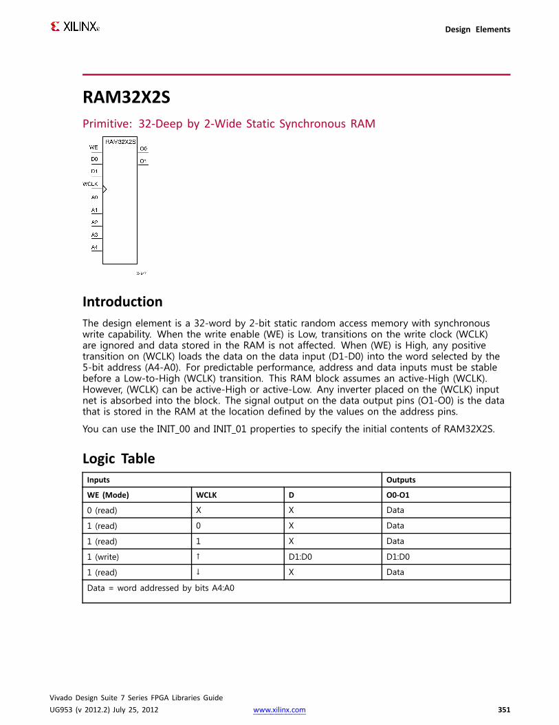
Design Elements
RAM32X2SPrimitive: 32-Deep by 2-Wide Static Synchronous RAM
IntroductionThe design element is a 32-word by 2-bit static random access memory with synchronouswrite capability. When the write enable (WE) is Low, transitions on the write clock (WCLK)are ignored and data stored in the RAM is not affected. When (WE) is High, any positivetransition on (WCLK) loads the data on the data input (D1-D0) into the word selected by the5-bit address (A4-A0). For predictable performance, address and data inputs must be stablebefore a Low-to-High (WCLK) transition. This RAM block assumes an active-High (WCLK).However, (WCLK) can be active-High or active-Low. Any inverter placed on the (WCLK) inputnet is absorbed into the block. The signal output on the data output pins (O1-O0) is the datathat is stored in the RAM at the location defined by the values on the address pins.
You can use the INIT_00 and INIT_01 properties to specify the initial contents of RAM32X2S.
Logic TableInputs Outputs
WE (Mode) WCLK D O0-O1
0 (read) X X Data
1 (read) 0 X Data
1 (read) 1 X Data
1 (write) ↑ D1:D0 D1:D0
1 (read) ↓ X Data
Data = word addressed by bits A4:A0
Vivado Design Suite 7 Series FPGA Libraries GuideUG953 (v 2012.2) July 25, 2012 www.xilinx.com 351

Design Elements
Design Entry MethodInstantiation Yes
Inference Recommended
CORE Generator™ and wizards No
Macro support No
Available AttributesAttribute Data Type Allowed Values Default Descriptions
INIT_00 Hexadecimal Any 32-Bit Value All zeros INIT for bit 0 of RAM.
INIT_01 Hexadecimal Any 32-Bit Value All zeros INIT for bit 1 of RAM.
VHDL Instantiation TemplateUnless they already exist, copy the following two statements and paste them before the entitydeclaration.Library UNISIM;use UNISIM.vcomponents.all;
-- RAM32X2S: 32 x 2 posedge write distributed (LUT) RAM (Mapped to SliceM LUT6)-- 7 Series-- Xilinx HDL Libraries Guide, version 2012.2
RAM32X2S_inst : RAM32X2Sgeneric map (
INIT_00 => X"00000000", -- INIT for bit 0 of RAMINIT_01 => X"00000000") -- INIT for bit 1 of RAM
port map (O0 => O0, -- RAMdata[0] outputO1 => O1, -- RAMdata[1] outputA0 => A0, -- RAMaddress[0] inputA1 => A1, -- RAMaddress[1] inputA2 => A2, -- RAMaddress[2] inputA3 => A3, -- RAMaddress[3] inputA4 => A4, -- RAMaddress[4] inputD0 => D0, -- RAMdata[0] inputD1 => D1, -- RAMdata[1] inputWCLK=> WCLK, -- Write clock inputWE => WE -- Write enable input
);
-- End of RAM32X2S_inst instantiation
Vivado Design Suite 7 Series FPGA Libraries GuideUG953 (v 2012.2) July 25, 2012 www.xilinx.com 352

Design Elements
Verilog Instantiation Template
// RAM32X2S: 32 x 2 posedge write distributed (LUT) RAM (Mapped to a SliceM LUT6)// 7 Series// Xilinx HDL Libraries Guide, version 2012.2
RAM32X2S#(.INIT_00(32'h00000000), // INIT forr bit 0 of RAM.INIT_01(32'h00000000) // INIT forr bit 1 of RAM
) RAM32X2S_inst (.O0(O0), // RAMdata[0] output.O1(O1), // RAMdata[1] output.A0(A0), // RAMaddress[0] input.A1(A1), // RAMaddress[1] input.A2(A2), // RAMaddress[2] input.A3(A3), // RAMaddress[3] input.A4(A4), // RAMaddress[4] input.D0(D0), // RAMdata[0] input.D1(D1), // RAMdata[1] input.WCLK(WCLK), // Write clock input.WE(WE) // Write enable input
);
// End of RAM32X2S_inst instantiation
For More InformationSee the 7 series FPGA User Documentation (User Guides and Data Sheets).
Vivado Design Suite 7 Series FPGA Libraries GuideUG953 (v 2012.2) July 25, 2012 www.xilinx.com 353

Design Elements
RAM64MPrimitive: 64-Deep by 4-bit Wide Multi Port Random Access Memory (SelectRAM)
IntroductionThis design element is a 64-bit deep by 4-bit wide, multi-port, random access memory withsynchronous write and asynchronous independent bit wide read capability. This RAM isimplemented using the LUT resources of the device (also known as SelectRAM™) and doesnot consume any of the block RAM resources of the device. The RAM64M component isimplemented in a single slice, and consists of one 4-bit write, 1-bit read port, and threeseparate 1-bit read ports from the same memory allowing for 4-bit write and independentbit read access RAM.
• If the DIA, DIB, DIC, and DID inputs are all tied to the same data inputs, the RAM canbecome a 1 read/write port, 3 independent read port 64x1 quad port memory.
• If DID is grounded, DOD is not used.
• If ADDRA, ADDRB, and ADDRC are tied to the same address, the RAM becomes a 64x3simple dual port RAM.
• If ADDRD is tied to ADDRA, ADDRB, and ADDRC, the RAM is a 64x4 single port RAM.
There are several other possible configurations for this RAM.
Vivado Design Suite 7 Series FPGA Libraries GuideUG953 (v 2012.2) July 25, 2012 www.xilinx.com 354
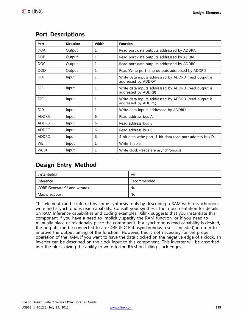
Design Elements
Port DescriptionsPort Direction Width Function
DOA Output 1 Read port data outputs addressed by ADDRA
DOB Output 1 Read port data outputs addressed by ADDRB
DOC Output 1 Read port data outputs addressed by ADDRC
DOD Output 1 Read/Write port data outputs addressed by ADDRD
DIA Input 1 Write data inputs addressed by ADDRD (read output isaddressed by ADDRA)
DIB Input 1 Write data inputs addressed by ADDRD (read output isaddressed by ADDRB)
DIC Input 1 Write data inputs addressed by ADDRD (read output isaddressed by ADDRC)
DID Input 1 Write data inputs addressed by ADDRD
ADDRA Input 6 Read address bus A
ADDRB Input 6 Read address bus B
ADDRC Input 6 Read address bus C
ADDRD Input 6 4-bit data write port, 1-bit data read port address bus D
WE Input 1 Write Enable
WCLK Input 1 Write clock (reads are asynchronous)
Design Entry MethodInstantiation Yes
Inference Recommended
CORE Generator™ and wizards No
Macro support No
This element can be inferred by some synthesis tools by describing a RAM with a synchronouswrite and asynchronous read capability. Consult your synthesis tool documentation for detailson RAM inference capabilities and coding examples. Xilinx suggests that you instantiate thiscomponent if you have a need to implicitly specify the RAM function, or if you need tomanually place or relationally place the component. If a synchronous read capability is desired,the outputs can be connected to an FDRE (FDCE if asynchronous reset is needed) in order toimprove the output timing of the function. However, this is not necessary for the properoperation of the RAM. If you want to have the data clocked on the negative edge of a clock, aninverter can be described on the clock input to this component. This inverter will be absorbedinto the block giving the ability to write to the RAM on falling clock edges.
Vivado Design Suite 7 Series FPGA Libraries GuideUG953 (v 2012.2) July 25, 2012 www.xilinx.com 355

Design Elements
If instantiated, the following connections should be made to this component:• Connect the WCLK input to the desired clock source, the DIA, DIB, DIC• Connect the DIA, DIB, DIC, and DID inputs to the data source to be stored• Connect the DOA, DOB, DOC, and DOD outputs to an FDCE D input or other appropriate
data destination, or leave unconnected if not used• Connect the WE clock enable pin to the proper write enable source in the design• Connect the ADDRD bus to the source for the read/write addressing• Connect the ADDRA, ADDRB, and ADDRC buses to the appropriate read address
connections
The optional INIT_A, INIT_B, INIT_C and INIT_D attributes let you specify the initial memorycontents of each port using a 64-bit hexadecimal value. The INIT value correlates to the RAMaddressing by the following equation: ADDRy[z] = INIT_y[z]. For instance, if the RAM ADDRCport is addressed to 00001, then the INIT_C[1] values would be the initial values shown on theDOC port before the first write occurs at that address. If left unspecified, the initial contents willdefault to all zeros.
Available AttributesAttribute Data Type Allowed Values Default Description
INIT_A Hexadecimal Any 64-Bit Value All zero Specifies the initial contents of theRAM on port A.
INIT_B Hexadecimal Any 64-Bit Value All zero Specifies the initial contents of theRAM on port B.
INIT_C Hexadecimal Any 64-Bit Value All zero Specifies the initial contents of theRAM on port C.
INIT_D Hexadecimal Any 64-Bit Value All zero Specifies the initial contents of theRAM on port D.
VHDL Instantiation TemplateUnless they already exist, copy the following two statements and paste them before the entitydeclaration.Library UNISIM;use UNISIM.vcomponents.all;
-- RAM64M: 64-deep by 4-wide Multi Port LUT RAM (Mapped to four SliceM LUT6s)-- 7 Series-- Xilinx HDL Libraries Guide, version 2012.2
RAM64M_inst : RAM64Mgeneric map (
INIT_A => X"0000000000000000", -- Initial contents of A portINIT_B => X"0000000000000000", -- Initial contents of B portINIT_C => X"0000000000000000", -- Initial contents of C portINIT_D => X"0000000000000000) -- Initial contents of D port
port map (DOA => DOA, -- Read port A 1-bit outputDOB => DOB, -- Read port B 1-bit outputDOC=> DOC, -- Read port C 1-bit outputDOD=> DOD, -- Read/Write port D 1-bit output
Vivado Design Suite 7 Series FPGA Libraries GuideUG953 (v 2012.2) July 25, 2012 www.xilinx.com 356
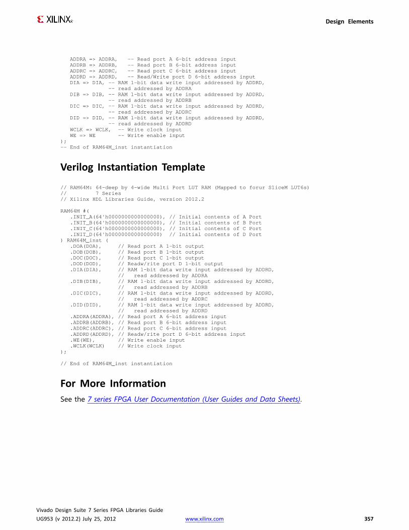
Design Elements
ADDRA=> ADDRA, -- Read port A 6-bit address inputADDRB=> ADDRB, -- Read port B 6-bit address inputADDRC=> ADDRC, -- Read port C 6-bit address inputADDRD=> ADDRD, -- Read/Write port D 6-bit address inputDIA => DIA, -- RAM1-bit data write input addressed by ADDRD,
-- read addressed by ADDRADIB => DIB, -- RAM1-bit data write input addressed by ADDRD,
-- read addressed by ADDRBDIC => DIC, -- RAM1-bit data write input addressed by ADDRD,
-- read addressed by ADDRCDID => DID, -- RAM1-bit data write input addressed by ADDRD,
-- read addressed by ADDRDWCLK=> WCLK, -- Write clock inputWE => WE -- Write enable input
);-- End of RAM64M_inst instantiation
Verilog Instantiation Template
// RAM64M: 64-deep by 4-wide Multi Port LUT RAM (Mapped to forur SliceM LUT6s)// 7 Series// Xilinx HDL Libraries Guide, version 2012.2
RAM64M#(.INIT_A(64'h0000000000000000), // Initial contents of A Port.INIT_B(64'h0000000000000000), // Initial contents of B Port.INIT_C(64'h0000000000000000), // Initial contents of C Port.INIT_D(64'h0000000000000000) // Initial contents of D Port
) RAM64M_inst (.DOA(DOA), // Read port A 1-bit output.DOB(DOB), // Read port B 1-bit output.DOC(DOC), // Read port C 1-bit output.DOD(DOD), // Readw/rite port D 1-bit output.DIA(DIA), // RAM1-bit data write input addressed by ADDRD,
// read addressed by ADDRA.DIB(DIB), // RAM1-bit data write input addressed by ADDRD,
// read addressed by ADDRB.DIC(DIC), // RAM1-bit data write input addressed by ADDRD,
// read addressed by ADDRC.DID(DID), // RAM1-bit data write input addressed by ADDRD,
// read addressed by ADDRD.ADDRA(ADDRA), // Read port A 6-bit address input.ADDRB(ADDRB), // Read port B 6-bit address input.ADDRC(ADDRC), // Read port C 6-bit address input.ADDRD(ADDRD), // Readw/rite port D 6-bit address input.WE(WE), // Write enable input.WCLK(WCLK) // Write clock input
);
// End of RAM64M_inst instantiation
For More InformationSee the 7 series FPGA User Documentation (User Guides and Data Sheets).
Vivado Design Suite 7 Series FPGA Libraries GuideUG953 (v 2012.2) July 25, 2012 www.xilinx.com 357

Design Elements
RAM64X1DPrimitive: 64-Deep by 1-Wide Dual Port Static Synchronous RAM
IntroductionThis design element is a 64-word by 1-bit static dual port random access memory withsynchronous write capability. The device has two separate address ports: the read address(DPRA5:DPRA0) and the write address (A5:A0). These two address ports are completelyasynchronous. The read address controls the location of the data driven out of the output pin(DPO), and the write address controls the destination of a valid write transaction. When thewrite enable (WE) is Low, transitions on the write clock (WCLK) are ignored and data stored inthe RAM is not affected.
When WE is High, any positive transition on WCLK loads the data on the data input (D) into theword selected by the 6-bit (A0:A5) write address. For predictable performance, write addressand data inputs must be stable before a Low-to-High WCLK transition. This RAM block assumesan active-High WCLK. WCLK can be active-High or active-Low. Any inverter placed on theWCLK input net is absorbed into the block.
The SPO output reflects the data in the memory cell addressed by A5:A0. The DPO outputreflects the data in the memory cell addressed by DPRA5:DPRA0.
Note The write process is not affected by the address on the read address port.
Logic TableInputs Outputs
WE (mode) WCLK D SPO DPO
0 (read) X X data_a data_d
1 (read) 0 X data_a data_d
1 (read) 1 X data_a data_d
1 (write) ↑ D D data_d
1 (read) ↓ X data_a data_d
Vivado Design Suite 7 Series FPGA Libraries GuideUG953 (v 2012.2) July 25, 2012 www.xilinx.com 358

Design Elements
Inputs Outputs
WE (mode) WCLK D SPO DPO
data_a = word addressed by bits A5:A0
data_d = word addressed by bits DPRA5:DPRA0
Design Entry MethodInstantiation Yes
Inference Recommended
CORE Generator™ and wizards No
Macro support No
Available AttributesAttribute Data Type Allowed Values Default Description
INIT Hexadecimal Any 64-BitValue
All zeros Initializes RAMs, registers, and look-uptables.
VHDL Instantiation TemplateUnless they already exist, copy the following two statements and paste them before the entitydeclaration.Library UNISIM;use UNISIM.vcomponents.all;
-- RAM64X1D: 64 x 1 negative edge write, asynchronous read-- dual-port distributed RAM (Mapped to SliceM LUT6)-- 7 Series-- Xilinx HDL Libraries Guide, version 2012.2
RAM64X1D_1_inst : RAM64X1D_1generic map (
INIT => X"0000000000000000") -- Initial contents of RAMport map (
DPO => DPO, -- Read-only 1-bit data outputSPO => SPO, -- R/W 1-bit data outputA0 => A0, -- R/W address[0] input bitA1 => A1, -- R/W address[1] input bitA2 => A2, -- R/W address[2] input bitA3 => A3, -- R/W address[3] input bitA4 => A4, -- R/W address[4] input bitA5 => A5, -- R/W address[5] input bitD => D, -- Write 1-bit data inputDPRA0 => DPRA0, -- Read-only address[0] input bitDPRA1 => DPRA1, -- Read-only address[1] input bitDPRA2 => DPRA2, -- Read-only address[2] input bitDPRA3 => DPRA3, -- Read-only address[3] input bitDPRA4 => DPRA4, -- Read-only address[4] input bitDPRA5 => DPRA5, -- Read-only address[5] input bitWCLK=> WCLK, -- Write clock inputWE => WE -- Write enable input
);
-- End of RAM64X1D_1_inst instantiation
Vivado Design Suite 7 Series FPGA Libraries GuideUG953 (v 2012.2) July 25, 2012 www.xilinx.com 359

Design Elements
Verilog Instantiation Template
// RAM64X1D: 64 x 1 positive edge write, asynchronous read dual-port distributed RAM (Mapped to a SliceM LUT6)// 7 Series// Xilinx HDL Libraries Guide, version 2012.2
RAM64X1D#(.INIT(64'h0000000000000000) // Initial contents of RAM
) RAM64X1D_inst (.DPO(DPO), // Read-only 1-bit data output.SPO(SPO), // Rw/ 1-bit data output.A0(A0), // Rw/ address[0] input bit.A1(A1), // Rw/ address[1] input bit.A2(A2), // Rw/ address[2] input bit.A3(A3), // Rw/ address[3] input bit.A4(A4), // Rw/ address[4] input bit.A5(A5), // Rw/ address[5] input bit.D(D), // Write 1-bit data input.DPRA0(DPRA0), // Read-only address[0] input bit.DPRA1(DPRA1), // Read-only address[1] input bit.DPRA2(DPRA2), // Read-only address[2] input bit.DPRA3(DPRA3), // Read-only address[3] input bit.DPRA4(DPRA4), // Read-only address[4] input bit.DPRA5(DPRA5), // Read-only address[5] input bit.WCLK(WCLK), // Write clock input.WE(WE) // Write enable input
);
// End of RAM64X1D_inst instantiation
For More InformationSee the 7 series FPGA User Documentation (User Guides and Data Sheets).
Vivado Design Suite 7 Series FPGA Libraries GuideUG953 (v 2012.2) July 25, 2012 www.xilinx.com 360

Design Elements
RAM64X1SPrimitive: 64-Deep by 1-Wide Static Synchronous RAM
IntroductionThis design element is a 64-word by 1-bit static random access memory (RAM) with synchronouswrite capability. When the write enable is set Low, transitions on the write clock (WCLK) areignored and data stored in the RAM is not affected. When WE is set High, any positive transitionon WCLK loads the data on the data input (D) into the word selected by the 6-bit address(A5:A0). This RAM block assumes an active-High WCLK. However, WCLK can be active-High oractive-Low. Any inverter placed on the WCLK input net is absorbed into the block.
The signal output on the data output pin (O) is the data that is stored in the RAM at thelocation defined by the values on the address pins.
You can initialize this element during configuration using the INIT attribute.
Logic TableMode selection is shown in the following logic tableInputs Outputs
WE (mode) WCLK D O
0 (read) X X Data
1 (read) 0 X Data
1 (read) 1 X Data
1 (write) ↑ D D
1 (read) ↓ X Data
Data = word addressed by bits A5:A0
Design Entry MethodInstantiation Yes
Inference Recommended
CORE Generator™ and wizards No
Macro support No
Vivado Design Suite 7 Series FPGA Libraries GuideUG953 (v 2012.2) July 25, 2012 www.xilinx.com 361
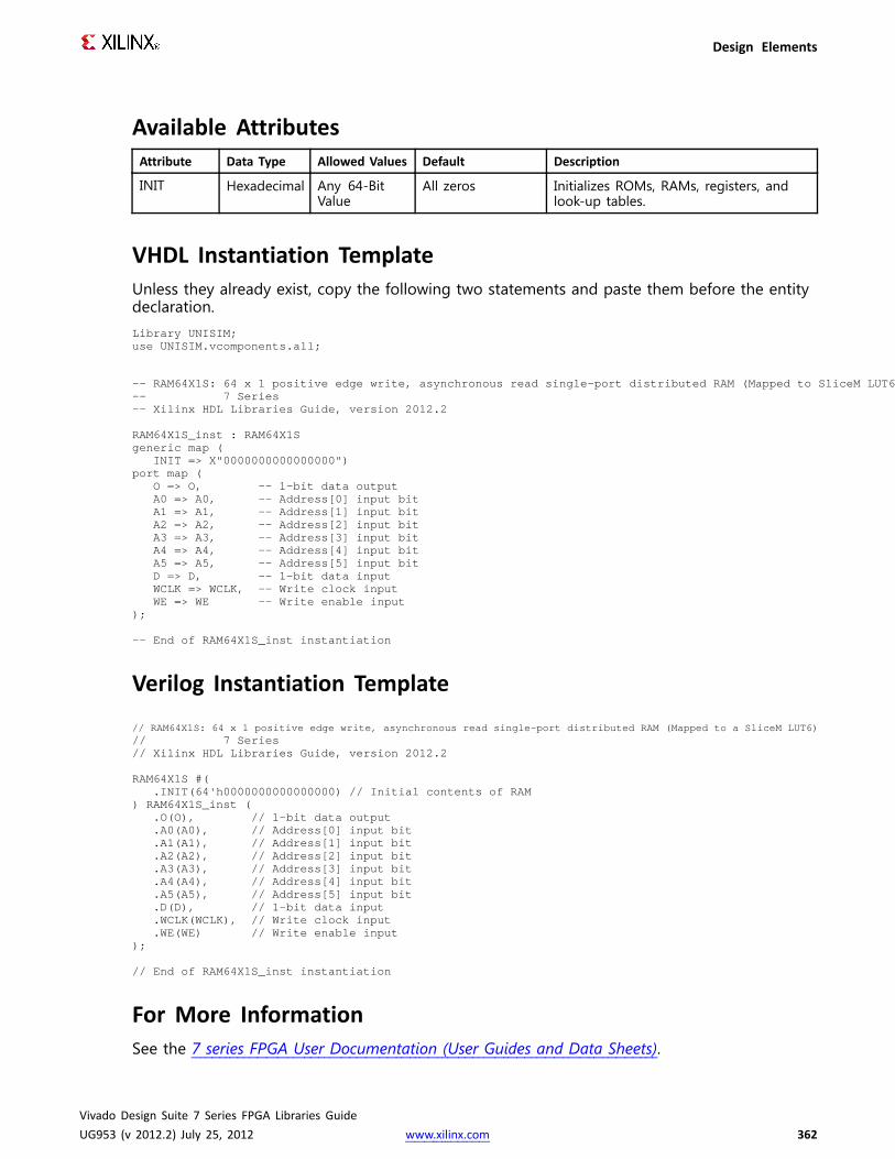
Design Elements
Available AttributesAttribute Data Type Allowed Values Default Description
INIT Hexadecimal Any 64-BitValue
All zeros Initializes ROMs, RAMs, registers, andlook-up tables.
VHDL Instantiation TemplateUnless they already exist, copy the following two statements and paste them before the entitydeclaration.Library UNISIM;use UNISIM.vcomponents.all;
-- RAM64X1S: 64 x 1 positive edge write, asynchronous read single-port distributed RAM (Mapped to SliceM LUT6)-- 7 Series-- Xilinx HDL Libraries Guide, version 2012.2
RAM64X1S_inst : RAM64X1Sgeneric map (
INIT => X"0000000000000000")port map (
O => O, -- 1-bit data outputA0 => A0, -- Address[0] input bitA1 => A1, -- Address[1] input bitA2 => A2, -- Address[2] input bitA3 => A3, -- Address[3] input bitA4 => A4, -- Address[4] input bitA5 => A5, -- Address[5] input bitD => D, -- 1-bit data inputWCLK=> WCLK, -- Write clock inputWE => WE -- Write enable input
);
-- End of RAM64X1S_inst instantiation
Verilog Instantiation Template
// RAM64X1S: 64 x 1 positive edge write, asynchronous read single-port distributed RAM (Mapped to a SliceM LUT6)// 7 Series// Xilinx HDL Libraries Guide, version 2012.2
RAM64X1S#(.INIT(64'h0000000000000000) // Initial contents of RAM
) RAM64X1S_inst (.O(O), // 1-bit data output.A0(A0), // Address[0] input bit.A1(A1), // Address[1] input bit.A2(A2), // Address[2] input bit.A3(A3), // Address[3] input bit.A4(A4), // Address[4] input bit.A5(A5), // Address[5] input bit.D(D), // 1-bit data input.WCLK(WCLK), // Write clock input.WE(WE) // Write enable input
);
// End of RAM64X1S_inst instantiation
For More InformationSee the 7 series FPGA User Documentation (User Guides and Data Sheets).
Vivado Design Suite 7 Series FPGA Libraries GuideUG953 (v 2012.2) July 25, 2012 www.xilinx.com 362
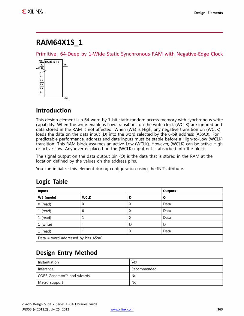
Design Elements
RAM64X1S_1Primitive: 64-Deep by 1-Wide Static Synchronous RAM with Negative-Edge Clock
IntroductionThis design element is a 64-word by 1-bit static random access memory with synchronous writecapability. When the write enable is Low, transitions on the write clock (WCLK) are ignored anddata stored in the RAM is not affected. When (WE) is High, any negative transition on (WCLK)loads the data on the data input (D) into the word selected by the 6-bit address (A5:A0). Forpredictable performance, address and data inputs must be stable before a High-to-Low (WCLK)transition. This RAM block assumes an active-Low (WCLK). However, (WCLK) can be active-Highor active-Low. Any inverter placed on the (WCLK) input net is absorbed into the block.
The signal output on the data output pin (O) is the data that is stored in the RAM at thelocation defined by the values on the address pins.
You can initialize this element during configuration using the INIT attribute.
Logic TableInputs Outputs
WE (mode) WCLK D O
0 (read) X X Data
1 (read) 0 X Data
1 (read) 1 X Data
1 (write) ↓ D D
1 (read) ↑ X Data
Data = word addressed by bits A5:A0
Design Entry MethodInstantiation Yes
Inference Recommended
CORE Generator™ and wizards No
Macro support No
Vivado Design Suite 7 Series FPGA Libraries GuideUG953 (v 2012.2) July 25, 2012 www.xilinx.com 363
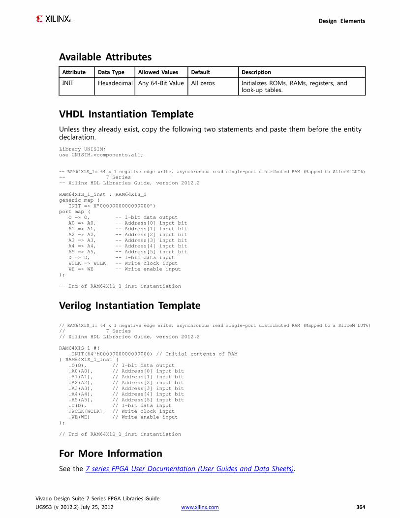
Design Elements
Available AttributesAttribute Data Type Allowed Values Default Description
INIT Hexadecimal Any 64-Bit Value All zeros Initializes ROMs, RAMs, registers, andlook-up tables.
VHDL Instantiation TemplateUnless they already exist, copy the following two statements and paste them before the entitydeclaration.Library UNISIM;use UNISIM.vcomponents.all;
-- RAM64X1S_1: 64 x 1 negative edge write, asynchronous read single-port distributed RAM (Mapped to SliceM LUT6)-- 7 Series-- Xilinx HDL Libraries Guide, version 2012.2
RAM64X1S_1_inst : RAM64X1S_1generic map (
INIT => X"0000000000000000")port map (
O => O, -- 1-bit data outputA0 => A0, -- Address[0] input bitA1 => A1, -- Address[1] input bitA2 => A2, -- Address[2] input bitA3 => A3, -- Address[3] input bitA4 => A4, -- Address[4] input bitA5 => A5, -- Address[5] input bitD => D, -- 1-bit data inputWCLK=> WCLK, -- Write clock inputWE => WE -- Write enable input
);
-- End of RAM64X1S_1_inst instantiation
Verilog Instantiation Template
// RAM64X1S_1: 64 x 1 negative edge write, asynchronous read single-port distributed RAM (Mapped to a SliceM LUT6)// 7 Series// Xilinx HDL Libraries Guide, version 2012.2
RAM64X1S_1 #(.INIT(64'h0000000000000000) // Initial contents of RAM
) RAM64X1S_1_inst (.O(O), // 1-bit data output.A0(A0), // Address[0] input bit.A1(A1), // Address[1] input bit.A2(A2), // Address[2] input bit.A3(A3), // Address[3] input bit.A4(A4), // Address[4] input bit.A5(A5), // Address[5] input bit.D(D), // 1-bit data input.WCLK(WCLK), // Write clock input.WE(WE) // Write enable input
);
// End of RAM64X1S_1_inst instantiation
For More InformationSee the 7 series FPGA User Documentation (User Guides and Data Sheets).
Vivado Design Suite 7 Series FPGA Libraries GuideUG953 (v 2012.2) July 25, 2012 www.xilinx.com 364

Design Elements
RAMB18E1Primitive: 18K-bit Configurable Synchronous Block RAM
Introduction7 series devices contain several block RAM memories that can be configured as FIFOs,automatic error correction RAM, or general-purpose 36KB or 18KB RAM/ROM memories. Theseblock RAM memories offer fast and flexible storage of large amounts of on-chip data. TheRAMB18E1 allows access to the block RAM in the 18KB configuration. This element can beconfigured and used as a 1-bit wide by 16K deep to an 18-bit wide by 1024-bit deep true dualport RAM. This element can also be configured as a 36-bit wide by 512 deep simple dualport RAM. Both read and write operations are fully synchronous to the supplied clock(s) tothe component. However, the READ and WRITE ports can operate fully independent andasynchronous to each other, accessing the same memory array. When configured in the widerdata width modes, byte-enable write operations are possible, and an optional output registercan be used to reduce the clock-to-out times of the RAM.
Vivado Design Suite 7 Series FPGA Libraries GuideUG953 (v 2012.2) July 25, 2012 www.xilinx.com 365
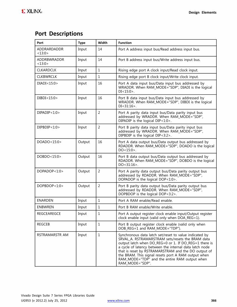
Design Elements
Port DescriptionsPort Type Width Function
ADDRARDADDR<13:0>
Input 14 Port A address input bus/Read address input bus.
ADDRBWRADDR<13:0>
Input 14 Port B address input bus/Write address input bus.
CLKARDCLK Input 1 Rising edge port A clock input/Read clock input.
CLKBWRCLK Input 1 Rising edge port B clock input/Write clock input.
DIADI<15:0> Input 16 Port A data input bus/Data input bus addressed byWRADDR. When RAM_MODE="SDP", DIADI is the logicalDI<15:0>.
DIBDI<15:0> Input 16 Port B data input bus/Data input bus addressed byWRADDR. When RAM_MODE="SDP", DIBDI is the logicalDI<31:16>.
DIPADIP<1:0> Input 2 Port A parity data input bus/Data parity input busaddressed by WRADDR. When RAM_MODE="SDP",DIPADIP is the logical DIP<1:0>.
DIPBDIP<1:0> Input 2 Port B parity data input bus/Data parity input busaddressed by WRADDR. When RAM_MODE="SDP",DIPBDIP is the logical DIP<3:2>.
DOADO<15:0> Output 16 Port A data output bus/Data output bus addressed byRDADDR. When RAM_MODE="SDP", DOADO is the logicalDO<15:0>.
DOBDO<15:0> Output 16 Port B data output bus/Data output bus addressed byRDADDR. When RAM_MODE="SDP", DOBDO is the logicalDO<31:16>.
DOPADOP<1:0> Output 2 Port A parity data output bus/Data parity output busaddressed by RDADDR. When RAM_MODE="SDP",DOPADOP is the logical DOP<1:0>.
DOPBDOP<1:0> Output 2 Port B parity data output bus/Data parity output busaddressed by RDADDR. When RAM_MODE="SDP",DOPBDOP is the logical DOP<3:2>.
ENARDEN Input 1 Port A RAM enable/Read enable.
ENBWREN Input 1 Port B RAM enable/Write enable.
REGCEAREGCE Input 1 Port A output register clock enable input/Output registerclock enable input (valid only when DOA_REG=1).
REGCEB Input 1 Port B output register clock enable (valid only whenDOB_REG=1 and RAM_MODE="TDP").
RSTRAMARSTR AM Input 1 Synchronous data latch set/reset to value indicated bySRVAL_A. RSTRAMARSTRAM sets/resets the BRAM dataoutput latch when DO_REG=0 or 1. If DO_REG=1 there isa cycle of latency between the internal data latch nodethat is reset by RSTRAMARSTRAM and the DO output ofthe BRAM. This signal resets port A RAM output whenRAM_MODE="TDP" and the entire RAM output whenRAM_MODE="SDP".
Vivado Design Suite 7 Series FPGA Libraries GuideUG953 (v 2012.2) July 25, 2012 www.xilinx.com 366

Design Elements
Port Type Width Function
RSTRAMB Input 1 Synchronous data latch set/reset to value indicated bySRVAL_B. RSTRAMB sets/resets the BRAM data outputlatch when DO_REG=0 or 1. If DO_REG=1 there is a cycleof latency between the internal data latch node that isreset by RSTRAMB and the DO output of the BRAM. Notused when RAM_MODE="SDP".
RSTREGARSTR EG Input 1 Synchronous output register set/reset to value indicated bySRVAL_A. RSTREGARSTREG sets/resets the output registerwhen DO_REG=1. RSTREG_PRIORITY_A determines if thissignal gets priority over REGCEAREGCE. This signal resetsport A output when RAM_MODE="TDP" and the entireoutput port when RAM_MODE="SDP".
RSTREGB Input 1 Synchronous output register set/reset to value indicatedby SRVAL_B. RSTREGB sets/resets the output registerwhen DO_REG=1. RSTREG_PRIORITY_B determines ifthis signal gets priority over REGCEB. Not used whenRAM_MODE="SDP".
WEA<1:0> Input 2 Port A byte-wide write enable. Not used whenRAM_MODE="SDP". See User Guide for WEA mapping fordifferent port widths.
WEBWE<3:0> Input 4 Port B byte-wide write enable/Write enable. See UserGuide for WEBWE mapping for different port widths.
Design Entry MethodInstantiation Yes
Inference Recommended
CORE Generator™ and wizards Yes
Macro support Yes
Available AttributesAttribute Type Allowed Values Default Description
RDADDR_COLLISION_HWCONFIG
STRING "DELAYED_WRITE","PERFORMANCE"
"DELAYED_WRITE" When set to "PERFORMANCE"allows for higher clockperformance (frequency) inREAD_FIRST mode. If using thesame clock on both ports ofthe RAM with "PERFORMANCE"mode, the address overlapcollision rules apply where in"DELAYED_WRITE" mode, youcan safely use the BRAM withoutincurring collisions.
SIM_COLLISION_CHECK
STRING "ALL","GENERATE_X_ONLY","NONE","WARNING_ONLY"
"ALL" Allows modification of thesimulation behavior so that if amemory collision occurs.
• "ALL" = warningproduced and affected
Vivado Design Suite 7 Series FPGA Libraries GuideUG953 (v 2012.2) July 25, 2012 www.xilinx.com 367
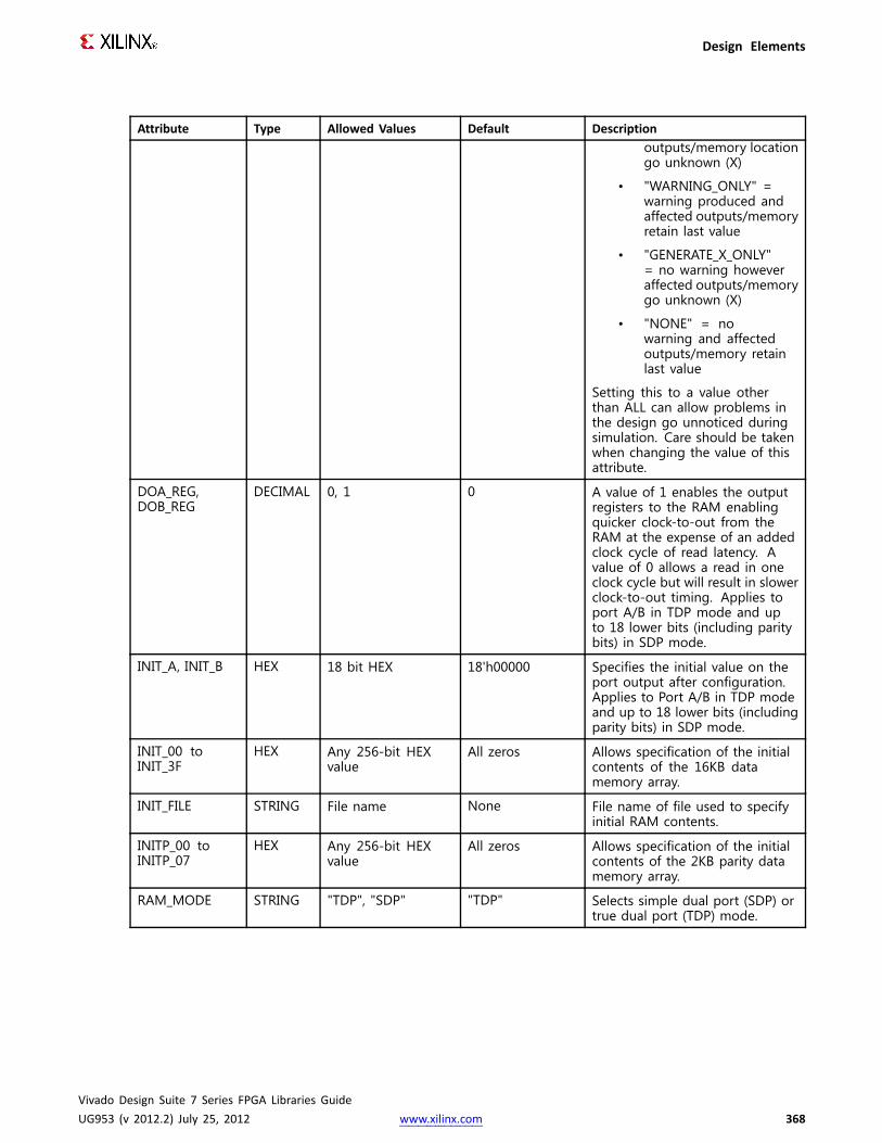
Design Elements
Attribute Type Allowed Values Default Descriptionoutputs/memory locationgo unknown (X)
• "WARNING_ONLY" =warning produced andaffected outputs/memoryretain last value
• "GENERATE_X_ONLY"= no warning howeveraffected outputs/memorygo unknown (X)
• "NONE" = nowarning and affectedoutputs/memory retainlast value
Setting this to a value otherthan ALL can allow problems inthe design go unnoticed duringsimulation. Care should be takenwhen changing the value of thisattribute.
DOA_REG,DOB_REG
DECIMAL 0, 1 0 A value of 1 enables the outputregisters to the RAM enablingquicker clock-to-out from theRAM at the expense of an addedclock cycle of read latency. Avalue of 0 allows a read in oneclock cycle but will result in slowerclock-to-out timing. Applies toport A/B in TDP mode and upto 18 lower bits (including paritybits) in SDP mode.
INIT_A, INIT_B HEX 18 bit HEX 18'h00000 Specifies the initial value on theport output after configuration.Applies to Port A/B in TDP modeand up to 18 lower bits (includingparity bits) in SDP mode.
INIT_00 toINIT_3F
HEX Any 256-bit HEXvalue
All zeros Allows specification of the initialcontents of the 16KB datamemory array.
INIT_FILE STRING File name None File name of file used to specifyinitial RAM contents.
INITP_00 toINITP_07
HEX Any 256-bit HEXvalue
All zeros Allows specification of the initialcontents of the 2KB parity datamemory array.
RAM_MODE STRING "TDP", "SDP" "TDP" Selects simple dual port (SDP) ortrue dual port (TDP) mode.
Vivado Design Suite 7 Series FPGA Libraries GuideUG953 (v 2012.2) July 25, 2012 www.xilinx.com 368

Design Elements
Attribute Type Allowed Values Default Description
READ_WIDTH_A DECIMAL 0, 1, 2, 4, 9, 18, 36,72
0 Specifies the desired data widthfor a read on Port A, includingparity bits. This value must be 0 ifthe Port A is not used. Otherwise,it should be set to the desiredport width. In "SDP" mode, thisis the read width including paritybits.
READ_WIDTH_B DECIMAL 0, 1, 2, 4, 9, 18 0 Specifies the desired data widthfor a read on Port B includingparity bits. This value must be 0 ifthe Port B is not used. Otherwise,it should be set to the desiredport width. Not used for "SDP"mode.
RSTREG_PRIORITY_A,RSTREG_PRIORITY_B
STRING "RSTREG", "REGCE" "RSTREG" Selects register priority forRSTREG or REGCE. Applies to portA/B in TDP mode and up to 18lower bits (including parity bits)in SDP mode.
SIM_DEVICE STRING 7SERIES "7SERIES" Must be set to "7SERIES" inorder to exhibit proper simulationbehavior under all conditions.
SRVAL_A,SRVAL_B
HEX 18 bit HEX 18'h00000 Specifies the output value ofthe RAM upon assertion of thesynchronous reset (RSTREG)signal.
WRITE_MODE_A,WRITE_MODE_B
STRING "WRITE_FIRST","NO_CHANGE","READ_FIRST"
"WRITE_FIRST" Specifies output behavior of theport being written to.
• "WRITE_FIRST" = writtenvalue appears on outputport of the RAM
• "READ_FIRST" = previousRAM contents for thatmemory location appearon the output port
• "NO_CHANGE" =previous value on theoutput port remains thesame.
When RAM_MODE="SDP",WRITE_MODE can not be set to"NO_CHANGE". For simple dualport implementations, you shouldgenerally set this attribute to"READ_FIRST" if using the sameclock on both ports and to set itto "WRITE_FIRST" if using differentclocks. This generally yields animproved collision or addressoverlap behavior when using theBRAM in this configuration.
Vivado Design Suite 7 Series FPGA Libraries GuideUG953 (v 2012.2) July 25, 2012 www.xilinx.com 369
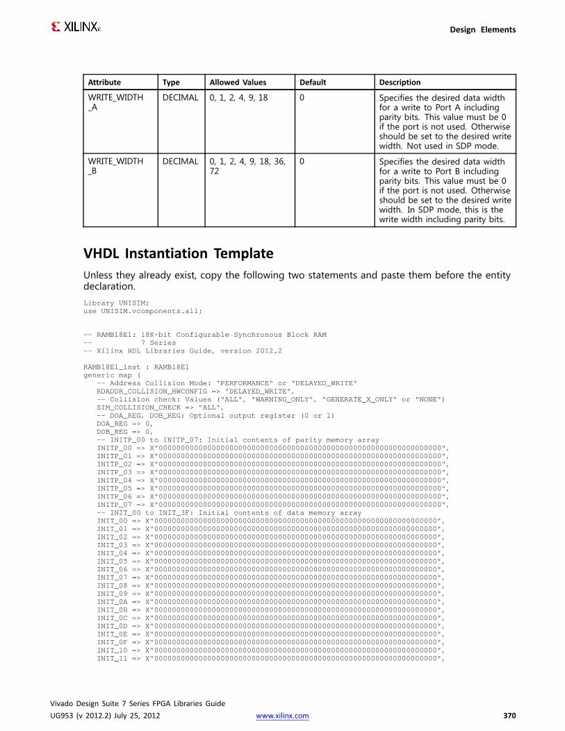
Design Elements
Attribute Type Allowed Values Default Description
WRITE_WIDTH_A
DECIMAL 0, 1, 2, 4, 9, 18 0 Specifies the desired data widthfor a write to Port A includingparity bits. This value must be 0if the port is not used. Otherwiseshould be set to the desired writewidth. Not used in SDP mode.
WRITE_WIDTH_B
DECIMAL 0, 1, 2, 4, 9, 18, 36,72
0 Specifies the desired data widthfor a write to Port B includingparity bits. This value must be 0if the port is not used. Otherwiseshould be set to the desired writewidth. In SDP mode, this is thewrite width including parity bits.
VHDL Instantiation TemplateUnless they already exist, copy the following two statements and paste them before the entitydeclaration.Library UNISIM;use UNISIM.vcomponents.all;
-- RAMB18E1: 18K-bit Configurable Synchronous Block RAM-- 7 Series-- Xilinx HDL Libraries Guide, version 2012.2
RAMB18E1_inst : RAMB18E1generic map (
-- Address Collision Mode: "PERFORMANCE"or "DELAYED_WRITE"RDADDR_COLLISION_HWCONFIG=> "DELAYED_WRITE",-- Collision check: Values ("ALL", "WARNING_ONLY", "GENERATE_X_ONLY"or "NONE")SIM_COLLISION_CHECK => "ALL",-- DOA_REG, DOB_REG: Optional output register (0 or 1)DOA_REG=> 0,DOB_REG=> 0,-- INITP_00 to INITP_07: Initial contents of parity memory arrayINITP_00 => X"0000000000000000000000000000000000000000000000000000000000000000",INITP_01 => X"0000000000000000000000000000000000000000000000000000000000000000",INITP_02 => X"0000000000000000000000000000000000000000000000000000000000000000",INITP_03 => X"0000000000000000000000000000000000000000000000000000000000000000",INITP_04 => X"0000000000000000000000000000000000000000000000000000000000000000",INITP_05 => X"0000000000000000000000000000000000000000000000000000000000000000",INITP_06 => X"0000000000000000000000000000000000000000000000000000000000000000",INITP_07 => X"0000000000000000000000000000000000000000000000000000000000000000",-- INIT_00 to INIT_3F: Initial contents of data memory arrayINIT_00 => X"0000000000000000000000000000000000000000000000000000000000000000",INIT_01 => X"0000000000000000000000000000000000000000000000000000000000000000",INIT_02 => X"0000000000000000000000000000000000000000000000000000000000000000",INIT_03 => X"0000000000000000000000000000000000000000000000000000000000000000",INIT_04 => X"0000000000000000000000000000000000000000000000000000000000000000",INIT_05 => X"0000000000000000000000000000000000000000000000000000000000000000",INIT_06 => X"0000000000000000000000000000000000000000000000000000000000000000",INIT_07 => X"0000000000000000000000000000000000000000000000000000000000000000",INIT_08 => X"0000000000000000000000000000000000000000000000000000000000000000",INIT_09 => X"0000000000000000000000000000000000000000000000000000000000000000",INIT_0A => X"0000000000000000000000000000000000000000000000000000000000000000",INIT_0B => X"0000000000000000000000000000000000000000000000000000000000000000",INIT_0C => X"0000000000000000000000000000000000000000000000000000000000000000",INIT_0D => X"0000000000000000000000000000000000000000000000000000000000000000",INIT_0E => X"0000000000000000000000000000000000000000000000000000000000000000",INIT_0F => X"0000000000000000000000000000000000000000000000000000000000000000",INIT_10 => X"0000000000000000000000000000000000000000000000000000000000000000",INIT_11 => X"0000000000000000000000000000000000000000000000000000000000000000",
Vivado Design Suite 7 Series FPGA Libraries GuideUG953 (v 2012.2) July 25, 2012 www.xilinx.com 370

Design Elements
INIT_12 => X"0000000000000000000000000000000000000000000000000000000000000000",INIT_13 => X"0000000000000000000000000000000000000000000000000000000000000000",INIT_14 => X"0000000000000000000000000000000000000000000000000000000000000000",INIT_15 => X"0000000000000000000000000000000000000000000000000000000000000000",INIT_16 => X"0000000000000000000000000000000000000000000000000000000000000000",INIT_17 => X"0000000000000000000000000000000000000000000000000000000000000000",INIT_18 => X"0000000000000000000000000000000000000000000000000000000000000000",INIT_19 => X"0000000000000000000000000000000000000000000000000000000000000000",INIT_1A => X"0000000000000000000000000000000000000000000000000000000000000000",INIT_1B => X"0000000000000000000000000000000000000000000000000000000000000000",INIT_1C => X"0000000000000000000000000000000000000000000000000000000000000000",INIT_1D => X"0000000000000000000000000000000000000000000000000000000000000000",INIT_1E => X"0000000000000000000000000000000000000000000000000000000000000000",INIT_1F => X"0000000000000000000000000000000000000000000000000000000000000000",INIT_20 => X"0000000000000000000000000000000000000000000000000000000000000000",INIT_21 => X"0000000000000000000000000000000000000000000000000000000000000000",INIT_22 => X"0000000000000000000000000000000000000000000000000000000000000000",INIT_23 => X"0000000000000000000000000000000000000000000000000000000000000000",INIT_24 => X"0000000000000000000000000000000000000000000000000000000000000000",INIT_25 => X"0000000000000000000000000000000000000000000000000000000000000000",INIT_26 => X"0000000000000000000000000000000000000000000000000000000000000000",INIT_27 => X"0000000000000000000000000000000000000000000000000000000000000000",INIT_28 => X"0000000000000000000000000000000000000000000000000000000000000000",INIT_29 => X"0000000000000000000000000000000000000000000000000000000000000000",INIT_2A => X"0000000000000000000000000000000000000000000000000000000000000000",INIT_2B => X"0000000000000000000000000000000000000000000000000000000000000000",INIT_2C => X"0000000000000000000000000000000000000000000000000000000000000000",INIT_2D => X"0000000000000000000000000000000000000000000000000000000000000000",INIT_2E => X"0000000000000000000000000000000000000000000000000000000000000000",INIT_2F => X"0000000000000000000000000000000000000000000000000000000000000000",INIT_30 => X"0000000000000000000000000000000000000000000000000000000000000000",INIT_31 => X"0000000000000000000000000000000000000000000000000000000000000000",INIT_32 => X"0000000000000000000000000000000000000000000000000000000000000000",INIT_33 => X"0000000000000000000000000000000000000000000000000000000000000000",INIT_34 => X"0000000000000000000000000000000000000000000000000000000000000000",INIT_35 => X"0000000000000000000000000000000000000000000000000000000000000000",INIT_36 => X"0000000000000000000000000000000000000000000000000000000000000000",INIT_37 => X"0000000000000000000000000000000000000000000000000000000000000000",INIT_38 => X"0000000000000000000000000000000000000000000000000000000000000000",INIT_39 => X"0000000000000000000000000000000000000000000000000000000000000000",INIT_3A => X"0000000000000000000000000000000000000000000000000000000000000000",INIT_3B => X"0000000000000000000000000000000000000000000000000000000000000000",INIT_3C => X"0000000000000000000000000000000000000000000000000000000000000000",INIT_3D => X"0000000000000000000000000000000000000000000000000000000000000000",INIT_3E => X"0000000000000000000000000000000000000000000000000000000000000000",INIT_3F => X"0000000000000000000000000000000000000000000000000000000000000000",-- INIT_A, INIT_B: Initial values on output portsINIT_A => X"00000",INIT_B => X"00000",-- Initialization File: RAM initialization fileINIT_FILE => "NONE",-- RAMMode: "SDP" or "TDP"RAM_MODE=> "TDP",-- READ_WIDTH_A/B, WRITE_WIDTH_A/B: Read/write width per portREAD_WIDTH_A=> 0, -- 0-72READ_WIDTH_B=> 0, -- 0-18WRITE_WIDTH_A=> 0, -- 0-18WRITE_WIDTH_B=> 0, -- 0-72-- RSTREG_PRIORITY_A, RSTREG_PRIORITY_B: Reset or enable priority ("RSTREG" or "REGCE")RSTREG_PRIORITY_A=> "RSTREG",RSTREG_PRIORITY_B=> "RSTREG",-- SRVAL_A, SRVAL_B: Set/reset value for outputSRVAL_A => X"00000",SRVAL_B => X"00000",-- Simulation Device: Must be set to "7SERIES" for simulation behaviorSIM_DEVICE => "7SERIES",-- WriteMode: Value on output upon a write ("WRITE_FIRST", "READ_FIRST", or "NO_CHANGE")WRITE_MODE_A=> "WRITE_FIRST",WRITE_MODE_B=> "WRITE_FIRST"
)port map (
-- Port A Data: 16-bit (each) output: Port A data
Vivado Design Suite 7 Series FPGA Libraries GuideUG953 (v 2012.2) July 25, 2012 www.xilinx.com 371
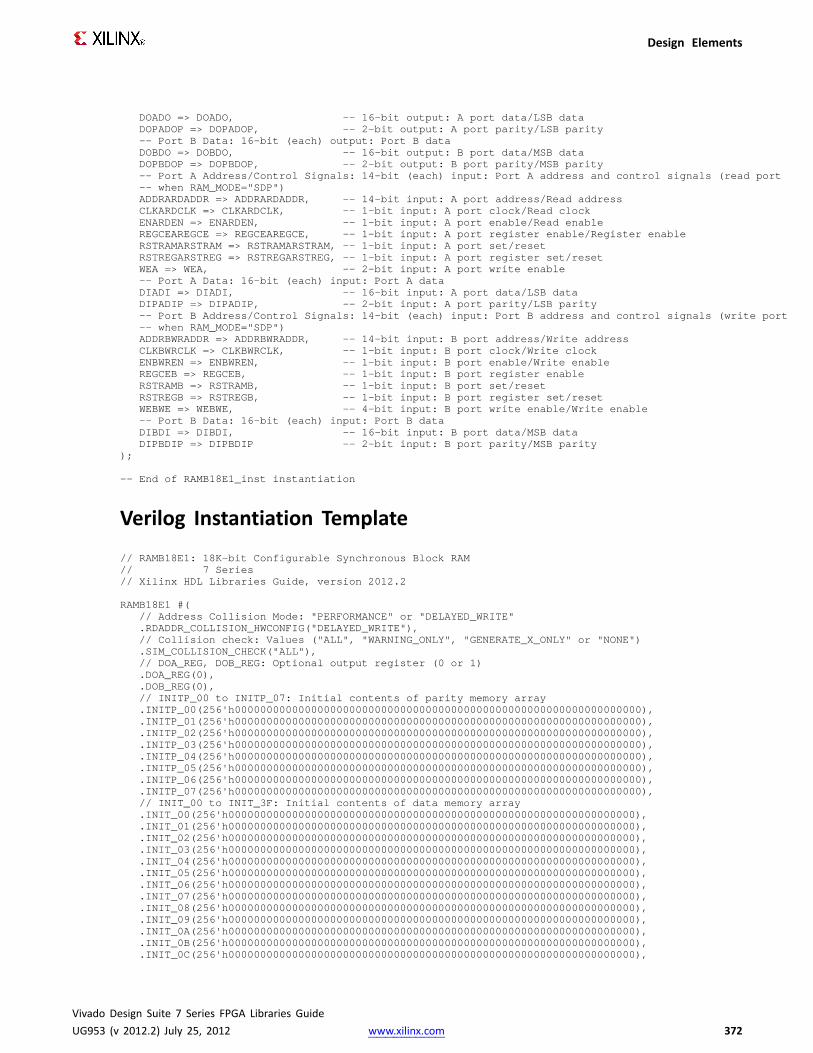
Design Elements
DOADO=> DOADO, -- 16-bit output: A port data/LSB dataDOPADOP=> DOPADOP, -- 2-bit output: A port parity/LSB parity-- Port B Data: 16-bit (each) output: Port B dataDOBDO=> DOBDO, -- 16-bit output: B port data/MSB dataDOPBDOP=> DOPBDOP, -- 2-bit output: B port parity/MSB parity-- Port A Address/Control Signals: 14-bit (each) input: Port A address and control signals (read port-- when RAM_MODE="SDP")ADDRARDADDR=> ADDRARDADDR, -- 14-bit input: A port address/Read addressCLKARDCLK=> CLKARDCLK, -- 1-bit input: A port clock/Read clockENARDEN=> ENARDEN, -- 1-bit input: A port enable/Read enableREGCEAREGCE=> REGCEAREGCE, -- 1-bit input: A port register enable/Register enableRSTRAMARSTRAM=> RSTRAMARSTRAM,-- 1-bit input: A port set/resetRSTREGARSTREG=> RSTREGARSTREG,-- 1-bit input: A port register set/resetWEA=> WEA, -- 2-bit input: A port write enable-- Port A Data: 16-bit (each) input: Port A dataDIADI => DIADI, -- 16-bit input: A port data/LSB dataDIPADIP => DIPADIP, -- 2-bit input: A port parity/LSB parity-- Port B Address/Control Signals: 14-bit (each) input: Port B address and control signals (write port-- when RAM_MODE="SDP")ADDRBWRADDR=> ADDRBWRADDR, -- 14-bit input: B port address/Write addressCLKBWRCLK=> CLKBWRCLK, -- 1-bit input: B port clock/Write clockENBWREN=> ENBWREN, -- 1-bit input: B port enable/Write enableREGCEB=> REGCEB, -- 1-bit input: B port register enableRSTRAMB=> RSTRAMB, -- 1-bit input: B port set/resetRSTREGB=> RSTREGB, -- 1-bit input: B port register set/resetWEBWE=> WEBWE, -- 4-bit input: B port write enable/Write enable-- Port B Data: 16-bit (each) input: Port B dataDIBDI => DIBDI, -- 16-bit input: B port data/MSB dataDIPBDIP => DIPBDIP -- 2-bit input: B port parity/MSB parity
);
-- End of RAMB18E1_inst instantiation
Verilog Instantiation Template
// RAMB18E1: 18K-bit Configurable Synchronous Block RAM// 7 Series// Xilinx HDL Libraries Guide, version 2012.2
RAMB18E1 #(// Address Collision Mode: "PERFORMANCE"or "DELAYED_WRITE".RDADDR_COLLISION_HWCONFIG("DELAYED_WRITE"),// Collision check: Values ("ALL", "WARNING_ONLY", "GENERATE_X_ONLY"or "NONE").SIM_COLLISION_CHECK("ALL"),// DOA_REG, DOB_REG: Optional output register (0 or 1).DOA_REG(0),.DOB_REG(0),// INITP_00 to INITP_07: Initial contents of parity memory array.INITP_00(256'h0000000000000000000000000000000000000000000000000000000000000000),.INITP_01(256'h0000000000000000000000000000000000000000000000000000000000000000),.INITP_02(256'h0000000000000000000000000000000000000000000000000000000000000000),.INITP_03(256'h0000000000000000000000000000000000000000000000000000000000000000),.INITP_04(256'h0000000000000000000000000000000000000000000000000000000000000000),.INITP_05(256'h0000000000000000000000000000000000000000000000000000000000000000),.INITP_06(256'h0000000000000000000000000000000000000000000000000000000000000000),.INITP_07(256'h0000000000000000000000000000000000000000000000000000000000000000),// INIT_00 to INIT_3F: Initial contents of data memory array.INIT_00(256'h0000000000000000000000000000000000000000000000000000000000000000),.INIT_01(256'h0000000000000000000000000000000000000000000000000000000000000000),.INIT_02(256'h0000000000000000000000000000000000000000000000000000000000000000),.INIT_03(256'h0000000000000000000000000000000000000000000000000000000000000000),.INIT_04(256'h0000000000000000000000000000000000000000000000000000000000000000),.INIT_05(256'h0000000000000000000000000000000000000000000000000000000000000000),.INIT_06(256'h0000000000000000000000000000000000000000000000000000000000000000),.INIT_07(256'h0000000000000000000000000000000000000000000000000000000000000000),.INIT_08(256'h0000000000000000000000000000000000000000000000000000000000000000),.INIT_09(256'h0000000000000000000000000000000000000000000000000000000000000000),.INIT_0A(256'h0000000000000000000000000000000000000000000000000000000000000000),.INIT_0B(256'h0000000000000000000000000000000000000000000000000000000000000000),.INIT_0C(256'h0000000000000000000000000000000000000000000000000000000000000000),
Vivado Design Suite 7 Series FPGA Libraries GuideUG953 (v 2012.2) July 25, 2012 www.xilinx.com 372
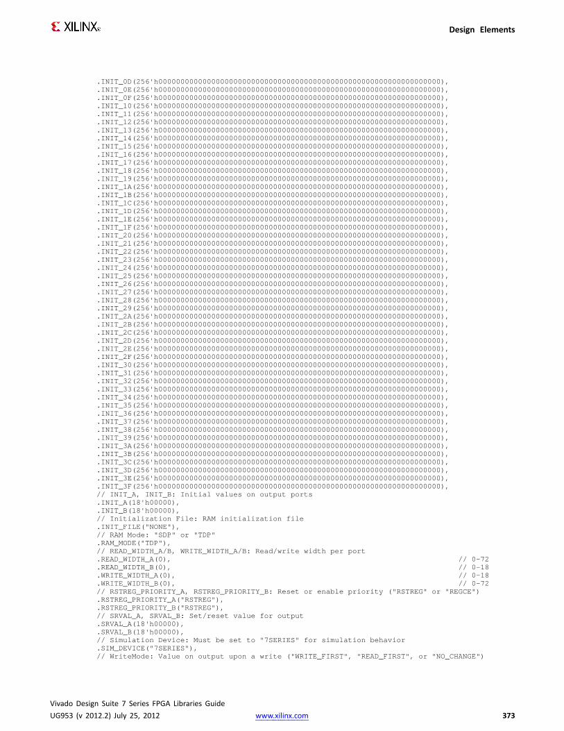
Design Elements
.INIT_0D(256'h0000000000000000000000000000000000000000000000000000000000000000),
.INIT_0E(256'h0000000000000000000000000000000000000000000000000000000000000000),
.INIT_0F(256'h0000000000000000000000000000000000000000000000000000000000000000),
.INIT_10(256'h0000000000000000000000000000000000000000000000000000000000000000),
.INIT_11(256'h0000000000000000000000000000000000000000000000000000000000000000),
.INIT_12(256'h0000000000000000000000000000000000000000000000000000000000000000),
.INIT_13(256'h0000000000000000000000000000000000000000000000000000000000000000),
.INIT_14(256'h0000000000000000000000000000000000000000000000000000000000000000),
.INIT_15(256'h0000000000000000000000000000000000000000000000000000000000000000),
.INIT_16(256'h0000000000000000000000000000000000000000000000000000000000000000),
.INIT_17(256'h0000000000000000000000000000000000000000000000000000000000000000),
.INIT_18(256'h0000000000000000000000000000000000000000000000000000000000000000),
.INIT_19(256'h0000000000000000000000000000000000000000000000000000000000000000),
.INIT_1A(256'h0000000000000000000000000000000000000000000000000000000000000000),
.INIT_1B(256'h0000000000000000000000000000000000000000000000000000000000000000),
.INIT_1C(256'h0000000000000000000000000000000000000000000000000000000000000000),
.INIT_1D(256'h0000000000000000000000000000000000000000000000000000000000000000),
.INIT_1E(256'h0000000000000000000000000000000000000000000000000000000000000000),
.INIT_1F(256'h0000000000000000000000000000000000000000000000000000000000000000),
.INIT_20(256'h0000000000000000000000000000000000000000000000000000000000000000),
.INIT_21(256'h0000000000000000000000000000000000000000000000000000000000000000),
.INIT_22(256'h0000000000000000000000000000000000000000000000000000000000000000),
.INIT_23(256'h0000000000000000000000000000000000000000000000000000000000000000),
.INIT_24(256'h0000000000000000000000000000000000000000000000000000000000000000),
.INIT_25(256'h0000000000000000000000000000000000000000000000000000000000000000),
.INIT_26(256'h0000000000000000000000000000000000000000000000000000000000000000),
.INIT_27(256'h0000000000000000000000000000000000000000000000000000000000000000),
.INIT_28(256'h0000000000000000000000000000000000000000000000000000000000000000),
.INIT_29(256'h0000000000000000000000000000000000000000000000000000000000000000),
.INIT_2A(256'h0000000000000000000000000000000000000000000000000000000000000000),
.INIT_2B(256'h0000000000000000000000000000000000000000000000000000000000000000),
.INIT_2C(256'h0000000000000000000000000000000000000000000000000000000000000000),
.INIT_2D(256'h0000000000000000000000000000000000000000000000000000000000000000),
.INIT_2E(256'h0000000000000000000000000000000000000000000000000000000000000000),
.INIT_2F(256'h0000000000000000000000000000000000000000000000000000000000000000),
.INIT_30(256'h0000000000000000000000000000000000000000000000000000000000000000),
.INIT_31(256'h0000000000000000000000000000000000000000000000000000000000000000),
.INIT_32(256'h0000000000000000000000000000000000000000000000000000000000000000),
.INIT_33(256'h0000000000000000000000000000000000000000000000000000000000000000),
.INIT_34(256'h0000000000000000000000000000000000000000000000000000000000000000),
.INIT_35(256'h0000000000000000000000000000000000000000000000000000000000000000),
.INIT_36(256'h0000000000000000000000000000000000000000000000000000000000000000),
.INIT_37(256'h0000000000000000000000000000000000000000000000000000000000000000),
.INIT_38(256'h0000000000000000000000000000000000000000000000000000000000000000),
.INIT_39(256'h0000000000000000000000000000000000000000000000000000000000000000),
.INIT_3A(256'h0000000000000000000000000000000000000000000000000000000000000000),
.INIT_3B(256'h0000000000000000000000000000000000000000000000000000000000000000),
.INIT_3C(256'h0000000000000000000000000000000000000000000000000000000000000000),
.INIT_3D(256'h0000000000000000000000000000000000000000000000000000000000000000),
.INIT_3E(256'h0000000000000000000000000000000000000000000000000000000000000000),
.INIT_3F(256'h0000000000000000000000000000000000000000000000000000000000000000),// INIT_A, INIT_B: Initial values on output ports.INIT_A(18'h00000),.INIT_B(18'h00000),// Initialization File: RAM initialization file.INIT_FILE("NONE"),// RAMMode: "SDP" or "TDP".RAM_MODE("TDP"),// READ_WIDTH_A/B, WRITE_WIDTH_A/B: Read/write width per port.READ_WIDTH_A(0), // 0-72.READ_WIDTH_B(0), // 0-18.WRITE_WIDTH_A(0), // 0-18.WRITE_WIDTH_B(0), // 0-72// RSTREG_PRIORITY_A, RSTREG_PRIORITY_B: Reset or enable priority ("RSTREG" or "REGCE").RSTREG_PRIORITY_A("RSTREG"),.RSTREG_PRIORITY_B("RSTREG"),// SRVAL_A, SRVAL_B: Set/reset value for output.SRVAL_A(18'h00000),.SRVAL_B(18'h00000),// Simulation Device: Must be set to "7SERIES" for simulation behavior.SIM_DEVICE("7SERIES"),// WriteMode: Value on output upon a write ("WRITE_FIRST", "READ_FIRST", or "NO_CHANGE")
Vivado Design Suite 7 Series FPGA Libraries GuideUG953 (v 2012.2) July 25, 2012 www.xilinx.com 373
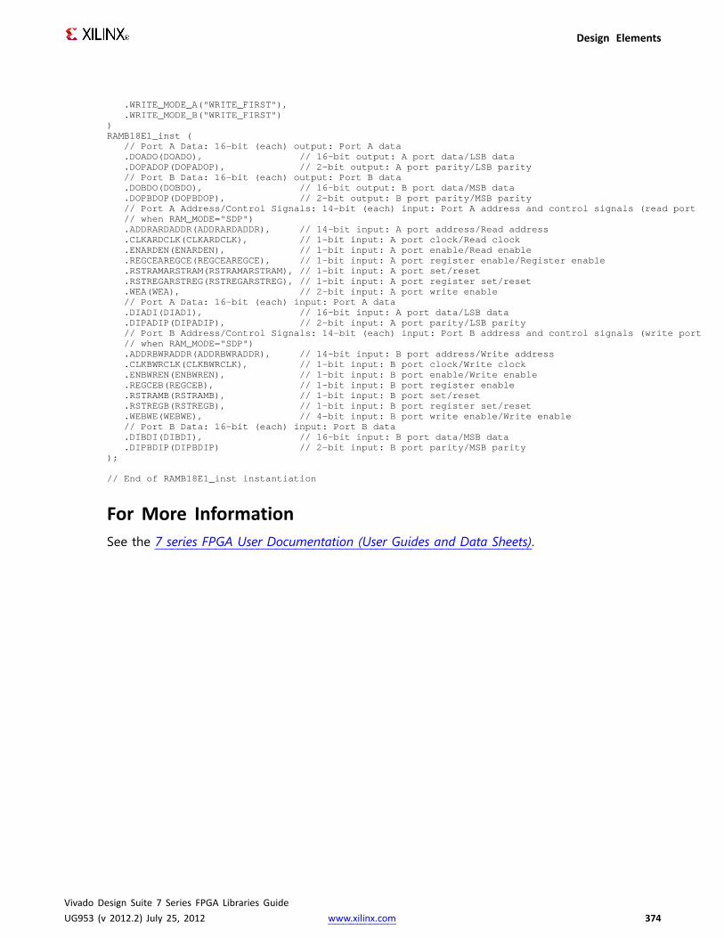
Design Elements
.WRITE_MODE_A("WRITE_FIRST"),
.WRITE_MODE_B("WRITE_FIRST"))RAMB18E1_inst (
// Port A Data: 16-bit (each) output: Port A data.DOADO(DOADO), // 16-bit output: A port data/LSB data.DOPADOP(DOPADOP), // 2-bit output: A port parity/LSB parity// Port B Data: 16-bit (each) output: Port B data.DOBDO(DOBDO), // 16-bit output: B port data/MSB data.DOPBDOP(DOPBDOP), // 2-bit output: B port parity/MSB parity// Port A Address/Control Signals: 14-bit (each) input: Port A address and control signals (read port// when RAM_MODE="SDP").ADDRARDADDR(ADDRARDADDR), // 14-bit input: A port address/Read address.CLKARDCLK(CLKARDCLK), // 1-bit input: A port clock/Read clock.ENARDEN(ENARDEN), // 1-bit input: A port enable/Read enable.REGCEAREGCE(REGCEAREGCE), // 1-bit input: A port register enable/Register enable.RSTRAMARSTRAM(RSTRAMARSTRAM),// 1-bit input: A port set/reset.RSTREGARSTREG(RSTREGARSTREG),// 1-bit input: A port register set/reset.WEA(WEA), // 2-bit input: A port write enable// Port A Data: 16-bit (each) input: Port A data.DIADI(DIADI), // 16-bit input: A port data/LSB data.DIPADIP(DIPADIP), // 2-bit input: A port parity/LSB parity// Port B Address/Control Signals: 14-bit (each) input: Port B address and control signals (write port// when RAM_MODE="SDP").ADDRBWRADDR(ADDRBWRADDR), // 14-bit input: B port address/Write address.CLKBWRCLK(CLKBWRCLK), // 1-bit input: B port clock/Write clock.ENBWREN(ENBWREN), // 1-bit input: B port enable/Write enable.REGCEB(REGCEB), // 1-bit input: B port register enable.RSTRAMB(RSTRAMB), // 1-bit input: B port set/reset.RSTREGB(RSTREGB), // 1-bit input: B port register set/reset.WEBWE(WEBWE), // 4-bit input: B port write enable/Write enable// Port B Data: 16-bit (each) input: Port B data.DIBDI(DIBDI), // 16-bit input: B port data/MSB data.DIPBDIP(DIPBDIP) // 2-bit input: B port parity/MSB parity
);
// End of RAMB18E1_inst instantiation
For More InformationSee the 7 series FPGA User Documentation (User Guides and Data Sheets).
Vivado Design Suite 7 Series FPGA Libraries GuideUG953 (v 2012.2) July 25, 2012 www.xilinx.com 374

Design Elements
RAMB36E1Primitive: 36K-bit Configurable Synchronous Block RAM
Vivado Design Suite 7 Series FPGA Libraries GuideUG953 (v 2012.2) July 25, 2012 www.xilinx.com 375

Design Elements
Introduction7 series devices contain several block RAM memories that can be configured as FIFOs,automatic error correction RAM, or general-purpose 36KB or 18KB RAM/ROM memories. Theseblock RAM memories offer fast and flexible storage of large amounts of on-chip data. TheRAMB36E1 allows access to the block RAM in the 36KB configuration. This element can becascaded to create a larger ram. This element can be configured and used as a 1-bit wide by32K deep to a 36-bit wide by 1K deep true dual port RAM. This element can also be configuredas a 72-bit wide by 512 deep simple dual port RAM. Both read and write operations are fullysynchronous to the supplied clock(s) to the component. However, the READ and WRITE portscan operate fully independent and asynchronous to each other, accessing the same memoryarray. When configured in the wider data width modes, byte-enable write operations arepossible, and an optional output register can be used to reduce the clock-to-out times ofthe RAM. Error detection and correction circuitry can also be enabled to uncover and rectifypossible memory corruptions.
Port DescriptionsPort Type Width Function
ADDRARDADDR<15:0>
Input 16 Port A address input bus/Read address input bus.
ADDRBWRADDR<15:0>
Input 16 Port B address input bus/Write address input bus.
CASCADEINA Input 1 Port A cascade input. Never use when RAM_MODE="SDP".
CASCADEINB Input 1 Port B cascade input. Never use when RAM_MODE="SDP".
CASCADEOUTA Output 1 Port A cascade output. Never use whenRAM_MODE="SDP".
CASCADEOUTB Output 1 Port B cascade output. Never use whenRAM_MODE="SDP".
CLKARDCLK Input 1 Rising edge port A clock input/Read clock input.
CLKBWRCLK Input 1 Rising edge port B clock input/Write clock input.
DBITERR Output 1 Status output from ECC function to indicate a doublebit error was detected. EN_ECC_READ needs to beTRUE in order to use this functionality. Not used whenRAM_MODE="TDP".
DIADI<31:0> Input 32 Port A data input bus/Data input bus addressed byWRADDR. When RAM_MODE="SDP", DIADI is the logicalDI<31:0>.
DIBDI<31:0> Input 32 Port B data input bus/Data input bus addressed byWRADDR. When RAM_MODE="SDP", DIBDI is the logicalDI<63:32>.
DIPADIP<3:0> Input 4 Port A parity data input bus/Data parity input busaddressed by WRADDR. When RAM_MODE="SDP",DIPADIP is the logical DIP<3:0>.
DIPBDIP<3:0> Input 4 Port B parity data input bus/Data parity input busaddressed by WRADDR. When RAM_MODE="SDP",DIPBDIP is the logical DIP<7:4>.
Vivado Design Suite 7 Series FPGA Libraries GuideUG953 (v 2012.2) July 25, 2012 www.xilinx.com 376
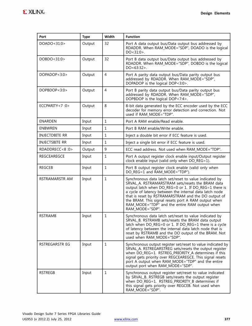
Design Elements
Port Type Width Function
DOADO<31:0> Output 32 Port A data output bus/Data output bus addressed byRDADDR. When RAM_MODE="SDP", DOADO is the logicalDO<31:0>.
DOBDO<31:0> Output 32 Port B data output bus/Data output bus addressed byRDADDR. When RAM_MODE="SDP", DOBDO is the logicalDO<63:32>.
DOPADOP<3:0> Output 4 Port A parity data output bus/Data parity output busaddressed by RDADDR. When RAM_MODE="SDP",DOPADOP is the logical DOP<3:0>.
DOPBDOP<3:0> Output 4 Port B parity data output bus/Data parity output busaddressed by RDADDR. When RAM_MODE="SDP",DOPBDOP is the logical DOP<7:4>.
ECCPARITY<7 :0> Output 8 8-bit data generated by the ECC encoder used by the ECCdecoder for memory error detection and correction. Notused if RAM_MODE="TDP".
ENARDEN Input 1 Port A RAM enable/Read enable.
ENBWREN Input 1 Port B RAM enable/Write enable.
INJECTDBITE RR Input 1 Inject a double bit error if ECC feature is used.
INJECTSBITE RR Input 1 Inject a single bit error if ECC feature is used.
RDADDRECC<8 :0> Output 9 ECC read address. Not used when RAM_MODE="TDP".
REGCEAREGCE Input 1 Port A output register clock enable input/Output registerclock enable input (valid only when DO_REG=1).
REGCEB Input 1 Port B output register clock enable (valid only whenDO_REG=1 and RAM_MODE="TDP").
RSTRAMARSTR AM Input 1 Synchronous data latch set/reset to value indicated bySRVAL_A. RSTRAMARSTRAM sets/resets the BRAM dataoutput latch when DO_REG=0 or 1. If DO_REG=1 there isa cycle of latency between the internal data latch nodethat is reset by RSTRAMARSTRAM and the DO output ofthe BRAM. This signal resets port A RAM output whenRAM_MODE="TDP" and the entire RAM output whenRAM_MODE="SDP".
RSTRAMB Input 1 Synchronous data latch set/reset to value indicated bySRVAL_B. RSTRAMB sets/resets the BRAM data outputlatch when DO_REG=0 or 1. If DO_REG=1 there is a cycleof latency between the internal data latch node that isreset by RSTRAMB and the DO output of the BRAM. Notused when RAM_MODE="SDP".
RSTREGARSTR EG Input 1 Synchronous output register set/reset to value indicated bySRVAL_A. RSTREGARSTREG sets/resets the output registerwhen DO_REG=1. RSTREG_PRIORITY_A determines if thissignal gets priority over REGCEAREGCE. This signal resetsport A output when RAM_MODE="TDP" and the entireoutput port when RAM_MODE="SDP".
RSTREGB Input 1 Synchronous output register set/reset to value indicatedby SRVAL_B. RSTREGB sets/resets the output registerwhen DO_REG=1. RSTREG_PRIORITY_B determines ifthis signal gets priority over REGCEB. Not used whenRAM_MODE="SDP".
Vivado Design Suite 7 Series FPGA Libraries GuideUG953 (v 2012.2) July 25, 2012 www.xilinx.com 377

Design Elements
Port Type Width Function
SBITERR Output 1 Status output from ECC function to indicate a singlebit error was detected. EN_ECC_READ needs to beTRUE in order to use this functionality. Not used whenRAM_MODE="TDP".
WEA<3:0> Input 4 Port A byte-wide write enable. Not used whenRAM_MODE="SDP". See User Guide for WEA mapping fordifferent port widths.
WEBWE<7:0> Input 8 Port B byte-wide write enable/Write enable. See UserGuide for WEBWE mapping for different port widths.
Design Entry MethodInstantiation Yes
Inference Recommended
CORE Generator™ and wizards Yes
Macro support Yes
Available AttributesAttribute Type Allowed Values Default Description
RDADDR_COLLISION_HWCONFIG
STRING "DELAYED_WRITE","PERFORMANCE"
"DELAYED_WRITE" When set to "PERFORMANCE"allows for higher clockperformance (frequency) inREAD_FIRST mode. If using thesame clock on both ports ofthe RAM with "PERFORMANCE"mode, the address overlapcollision rules apply where in"DELAYED_WRITE" mode, youcan safely use the BRAM withoutincurring collisions.
SIM_COLLISION_CHECK
STRING "ALL","GENERATE_X_ONLY","NONE","WARNING_ONLY"
"ALL" Allows modification of thesimulation behavior so that if amemory collision occurs
• "ALL" = warningproduced and affectedoutputs/memorylocation go unknown(X)
• "WARNING_ONLY" =warning producedand affectedoutputs/memory retainlast value
• "GENERATE_X_ONLY"= no warninghowever affectedoutputs/memory gounknown (X)
Vivado Design Suite 7 Series FPGA Libraries GuideUG953 (v 2012.2) July 25, 2012 www.xilinx.com 378
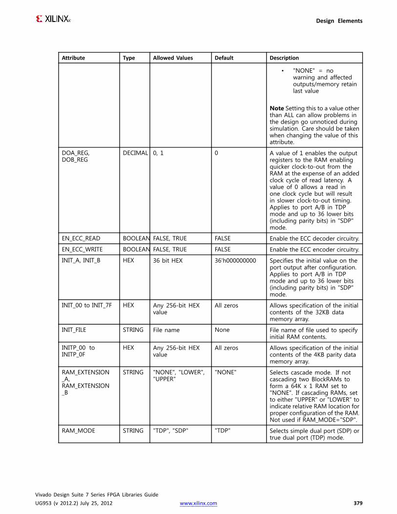
Design Elements
Attribute Type Allowed Values Default Description
• "NONE" = nowarning and affectedoutputs/memory retainlast value
Note Setting this to a value otherthan ALL can allow problems inthe design go unnoticed duringsimulation. Care should be takenwhen changing the value of thisattribute.
DOA_REG,DOB_REG
DECIMAL 0, 1 0 A value of 1 enables the outputregisters to the RAM enablingquicker clock-to-out from theRAM at the expense of an addedclock cycle of read latency. Avalue of 0 allows a read inone clock cycle but will resultin slower clock-to-out timing.Applies to port A/B in TDPmode and up to 36 lower bits(including parity bits) in "SDP"mode.
EN_ECC_READ BOOLEAN FALSE, TRUE FALSE Enable the ECC decoder circuitry.
EN_ECC_WRITE BOOLEAN FALSE, TRUE FALSE Enable the ECC encoder circuitry.
INIT_A, INIT_B HEX 36 bit HEX 36'h000000000 Specifies the initial value on theport output after configuration.Applies to port A/B in TDPmode and up to 36 lower bits(including parity bits) in "SDP"mode.
INIT_00 to INIT_7F HEX Any 256-bit HEXvalue
All zeros Allows specification of the initialcontents of the 32KB datamemory array.
INIT_FILE STRING File name None File name of file used to specifyinitial RAM contents.
INITP_00 toINITP_0F
HEX Any 256-bit HEXvalue
All zeros Allows specification of the initialcontents of the 4KB parity datamemory array.
RAM_EXTENSION_A,RAM_EXTENSION_B
STRING "NONE", "LOWER","UPPER"
"NONE" Selects cascade mode. If notcascading two BlockRAMs toform a 64K x 1 RAM set to"NONE". If cascading RAMs, setto either "UPPER" or "LOWER" toindicate relative RAM location forproper configuration of the RAM.Not used if RAM_MODE="SDP".
RAM_MODE STRING "TDP", "SDP" "TDP" Selects simple dual port (SDP) ortrue dual port (TDP) mode.
Vivado Design Suite 7 Series FPGA Libraries GuideUG953 (v 2012.2) July 25, 2012 www.xilinx.com 379

Design Elements
Attribute Type Allowed Values Default Description
READ_WIDTH_A,READ_WIDTH_B,WRITE_WIDTH _A,WRITE_WIDTH _B
DECIMAL 0, 1, 2, 4, 9, 18, 36,72
0 Specifies the desired data widthfor a read/write on port A/B,including parity bits. This valuemust be 0 if the port is not used.Otherwise, it should be set tothe desired port width.
RSTREG_PRIORITY_A,RSTREG_PRIORITY_B
STRING "RSTREG", "REGCE" "RSTREG" Selects register priority for"RSTREG" or "REGCE". Appliesto port A/B in TDP mode and upto 18 lower bits (including paritybits) in SDP mode.
SIM_DEVICE STRING 7SERIES "7SERIES" Must be set to "7SERIES"in order to exhibit propersimulation behavior under allconditions.
SRVAL_A, SRVAL_B HEX 36 bit HEX 36'h000000000 Specifies the output value ofthe RAM upon assertion of thesynchronous reset (RSTREG)signal.
WRITE_MODE_A,WRITE_MODE_B
STRING "WRITE_FIRST","NO_CHANGE","READ_FIRST"
"WRITE_FIRST" Specifies output behavior of theport being written to.
• "WRITE_FIRST" = writtenvalue appears on outputport of the RAM
• "READ_FIRST" =previous RAM contentsfor that memorylocation appears onthe output port
• "NO_CHANGE" =previous value on theoutput port remains thesame
When RAM_MODE="SDP",WRITE_MODE can not be setto "NO_CHANGE". For simpledual port implementations,your should generally setWRITE_MODE to "READ_FIRST"if using the same clock onboth ports and to set it to"WRITE_FIRST" if using differentclocks. This generally yields animproved collision or addressoverlap behavior when using theBRAM in this configuration.
VHDL Instantiation TemplateUnless they already exist, copy the following two statements and paste them before the entitydeclaration.Library UNISIM;
Vivado Design Suite 7 Series FPGA Libraries GuideUG953 (v 2012.2) July 25, 2012 www.xilinx.com 380
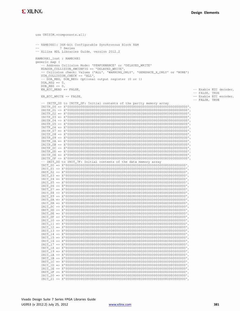
Design Elements
use UNISIM.vcomponents.all;
-- RAMB36E1: 36K-bit Configurable Synchronous Block RAM-- 7 Series-- Xilinx HDL Libraries Guide, version 2012.2
RAMB36E1_inst : RAMB36E1generic map (
-- Address Collision Mode: "PERFORMANCE"or "DELAYED_WRITE"RDADDR_COLLISION_HWCONFIG=> "DELAYED_WRITE",-- Collision check: Values ("ALL", "WARNING_ONLY", "GENERATE_X_ONLY"or "NONE")SIM_COLLISION_CHECK => "ALL",-- DOA_REG, DOB_REG: Optional output register (0 or 1)DOA_REG=> 0,DOB_REG=> 0,EN_ECC_READ=> FALSE, -- Enable ECC decoder,
-- FALSE, TRUEEN_ECC_WRITE=> FALSE, -- Enable ECC encoder,
-- FALSE, TRUE-- INITP_00 to INITP_0F: Initial contents of the parity memory arrayINITP_00 => X"0000000000000000000000000000000000000000000000000000000000000000",INITP_01 => X"0000000000000000000000000000000000000000000000000000000000000000",INITP_02 => X"0000000000000000000000000000000000000000000000000000000000000000",INITP_03 => X"0000000000000000000000000000000000000000000000000000000000000000",INITP_04 => X"0000000000000000000000000000000000000000000000000000000000000000",INITP_05 => X"0000000000000000000000000000000000000000000000000000000000000000",INITP_06 => X"0000000000000000000000000000000000000000000000000000000000000000",INITP_07 => X"0000000000000000000000000000000000000000000000000000000000000000",INITP_08 => X"0000000000000000000000000000000000000000000000000000000000000000",INITP_09 => X"0000000000000000000000000000000000000000000000000000000000000000",INITP_0A => X"0000000000000000000000000000000000000000000000000000000000000000",INITP_0B => X"0000000000000000000000000000000000000000000000000000000000000000",INITP_0C => X"0000000000000000000000000000000000000000000000000000000000000000",INITP_0D => X"0000000000000000000000000000000000000000000000000000000000000000",INITP_0E => X"0000000000000000000000000000000000000000000000000000000000000000",INITP_0F => X"0000000000000000000000000000000000000000000000000000000000000000",-- INIT_00 to INIT_7F: Initial contents of the data memory arrayINIT_00 => X"0000000000000000000000000000000000000000000000000000000000000000",INIT_01 => X"0000000000000000000000000000000000000000000000000000000000000000",INIT_02 => X"0000000000000000000000000000000000000000000000000000000000000000",INIT_03 => X"0000000000000000000000000000000000000000000000000000000000000000",INIT_04 => X"0000000000000000000000000000000000000000000000000000000000000000",INIT_05 => X"0000000000000000000000000000000000000000000000000000000000000000",INIT_06 => X"0000000000000000000000000000000000000000000000000000000000000000",INIT_07 => X"0000000000000000000000000000000000000000000000000000000000000000",INIT_08 => X"0000000000000000000000000000000000000000000000000000000000000000",INIT_09 => X"0000000000000000000000000000000000000000000000000000000000000000",INIT_0A => X"0000000000000000000000000000000000000000000000000000000000000000",INIT_0B => X"0000000000000000000000000000000000000000000000000000000000000000",INIT_0C => X"0000000000000000000000000000000000000000000000000000000000000000",INIT_0D => X"0000000000000000000000000000000000000000000000000000000000000000",INIT_0E => X"0000000000000000000000000000000000000000000000000000000000000000",INIT_0F => X"0000000000000000000000000000000000000000000000000000000000000000",INIT_10 => X"0000000000000000000000000000000000000000000000000000000000000000",INIT_11 => X"0000000000000000000000000000000000000000000000000000000000000000",INIT_12 => X"0000000000000000000000000000000000000000000000000000000000000000",INIT_13 => X"0000000000000000000000000000000000000000000000000000000000000000",INIT_14 => X"0000000000000000000000000000000000000000000000000000000000000000",INIT_15 => X"0000000000000000000000000000000000000000000000000000000000000000",INIT_16 => X"0000000000000000000000000000000000000000000000000000000000000000",INIT_17 => X"0000000000000000000000000000000000000000000000000000000000000000",INIT_18 => X"0000000000000000000000000000000000000000000000000000000000000000",INIT_19 => X"0000000000000000000000000000000000000000000000000000000000000000",INIT_1A => X"0000000000000000000000000000000000000000000000000000000000000000",INIT_1B => X"0000000000000000000000000000000000000000000000000000000000000000",INIT_1C => X"0000000000000000000000000000000000000000000000000000000000000000",INIT_1D => X"0000000000000000000000000000000000000000000000000000000000000000",INIT_1E => X"0000000000000000000000000000000000000000000000000000000000000000",INIT_1F => X"0000000000000000000000000000000000000000000000000000000000000000",INIT_20 => X"0000000000000000000000000000000000000000000000000000000000000000",INIT_21 => X"0000000000000000000000000000000000000000000000000000000000000000",
Vivado Design Suite 7 Series FPGA Libraries GuideUG953 (v 2012.2) July 25, 2012 www.xilinx.com 381

Design Elements
INIT_22 => X"0000000000000000000000000000000000000000000000000000000000000000",INIT_23 => X"0000000000000000000000000000000000000000000000000000000000000000",INIT_24 => X"0000000000000000000000000000000000000000000000000000000000000000",INIT_25 => X"0000000000000000000000000000000000000000000000000000000000000000",INIT_26 => X"0000000000000000000000000000000000000000000000000000000000000000",INIT_27 => X"0000000000000000000000000000000000000000000000000000000000000000",INIT_28 => X"0000000000000000000000000000000000000000000000000000000000000000",INIT_29 => X"0000000000000000000000000000000000000000000000000000000000000000",INIT_2A => X"0000000000000000000000000000000000000000000000000000000000000000",INIT_2B => X"0000000000000000000000000000000000000000000000000000000000000000",INIT_2C => X"0000000000000000000000000000000000000000000000000000000000000000",INIT_2D => X"0000000000000000000000000000000000000000000000000000000000000000",INIT_2E => X"0000000000000000000000000000000000000000000000000000000000000000",INIT_2F => X"0000000000000000000000000000000000000000000000000000000000000000",INIT_30 => X"0000000000000000000000000000000000000000000000000000000000000000",INIT_31 => X"0000000000000000000000000000000000000000000000000000000000000000",INIT_32 => X"0000000000000000000000000000000000000000000000000000000000000000",INIT_33 => X"0000000000000000000000000000000000000000000000000000000000000000",INIT_34 => X"0000000000000000000000000000000000000000000000000000000000000000",INIT_35 => X"0000000000000000000000000000000000000000000000000000000000000000",INIT_36 => X"0000000000000000000000000000000000000000000000000000000000000000",INIT_37 => X"0000000000000000000000000000000000000000000000000000000000000000",INIT_38 => X"0000000000000000000000000000000000000000000000000000000000000000",INIT_39 => X"0000000000000000000000000000000000000000000000000000000000000000",INIT_3A => X"0000000000000000000000000000000000000000000000000000000000000000",INIT_3B => X"0000000000000000000000000000000000000000000000000000000000000000",INIT_3C => X"0000000000000000000000000000000000000000000000000000000000000000",INIT_3D => X"0000000000000000000000000000000000000000000000000000000000000000",INIT_3E => X"0000000000000000000000000000000000000000000000000000000000000000",INIT_3F => X"0000000000000000000000000000000000000000000000000000000000000000",INIT_40 => X"0000000000000000000000000000000000000000000000000000000000000000",INIT_41 => X"0000000000000000000000000000000000000000000000000000000000000000",INIT_42 => X"0000000000000000000000000000000000000000000000000000000000000000",INIT_43 => X"0000000000000000000000000000000000000000000000000000000000000000",INIT_44 => X"0000000000000000000000000000000000000000000000000000000000000000",INIT_45 => X"0000000000000000000000000000000000000000000000000000000000000000",INIT_46 => X"0000000000000000000000000000000000000000000000000000000000000000",INIT_47 => X"0000000000000000000000000000000000000000000000000000000000000000",INIT_48 => X"0000000000000000000000000000000000000000000000000000000000000000",INIT_49 => X"0000000000000000000000000000000000000000000000000000000000000000",INIT_4A => X"0000000000000000000000000000000000000000000000000000000000000000",INIT_4B => X"0000000000000000000000000000000000000000000000000000000000000000",INIT_4C => X"0000000000000000000000000000000000000000000000000000000000000000",INIT_4D => X"0000000000000000000000000000000000000000000000000000000000000000",INIT_4E => X"0000000000000000000000000000000000000000000000000000000000000000",INIT_4F => X"0000000000000000000000000000000000000000000000000000000000000000",INIT_50 => X"0000000000000000000000000000000000000000000000000000000000000000",INIT_51 => X"0000000000000000000000000000000000000000000000000000000000000000",INIT_52 => X"0000000000000000000000000000000000000000000000000000000000000000",INIT_53 => X"0000000000000000000000000000000000000000000000000000000000000000",INIT_54 => X"0000000000000000000000000000000000000000000000000000000000000000",INIT_55 => X"0000000000000000000000000000000000000000000000000000000000000000",INIT_56 => X"0000000000000000000000000000000000000000000000000000000000000000",INIT_57 => X"0000000000000000000000000000000000000000000000000000000000000000",INIT_58 => X"0000000000000000000000000000000000000000000000000000000000000000",INIT_59 => X"0000000000000000000000000000000000000000000000000000000000000000",INIT_5A => X"0000000000000000000000000000000000000000000000000000000000000000",INIT_5B => X"0000000000000000000000000000000000000000000000000000000000000000",INIT_5C => X"0000000000000000000000000000000000000000000000000000000000000000",INIT_5D => X"0000000000000000000000000000000000000000000000000000000000000000",INIT_5E => X"0000000000000000000000000000000000000000000000000000000000000000",INIT_5F => X"0000000000000000000000000000000000000000000000000000000000000000",INIT_60 => X"0000000000000000000000000000000000000000000000000000000000000000",INIT_61 => X"0000000000000000000000000000000000000000000000000000000000000000",INIT_62 => X"0000000000000000000000000000000000000000000000000000000000000000",INIT_63 => X"0000000000000000000000000000000000000000000000000000000000000000",INIT_64 => X"0000000000000000000000000000000000000000000000000000000000000000",INIT_65 => X"0000000000000000000000000000000000000000000000000000000000000000",INIT_66 => X"0000000000000000000000000000000000000000000000000000000000000000",INIT_67 => X"0000000000000000000000000000000000000000000000000000000000000000",INIT_68 => X"0000000000000000000000000000000000000000000000000000000000000000",INIT_69 => X"0000000000000000000000000000000000000000000000000000000000000000",
Vivado Design Suite 7 Series FPGA Libraries GuideUG953 (v 2012.2) July 25, 2012 www.xilinx.com 382

Design Elements
INIT_6A => X"0000000000000000000000000000000000000000000000000000000000000000",INIT_6B => X"0000000000000000000000000000000000000000000000000000000000000000",INIT_6C => X"0000000000000000000000000000000000000000000000000000000000000000",INIT_6D => X"0000000000000000000000000000000000000000000000000000000000000000",INIT_6E => X"0000000000000000000000000000000000000000000000000000000000000000",INIT_6F => X"0000000000000000000000000000000000000000000000000000000000000000",INIT_70 => X"0000000000000000000000000000000000000000000000000000000000000000",INIT_71 => X"0000000000000000000000000000000000000000000000000000000000000000",INIT_72 => X"0000000000000000000000000000000000000000000000000000000000000000",INIT_73 => X"0000000000000000000000000000000000000000000000000000000000000000",INIT_74 => X"0000000000000000000000000000000000000000000000000000000000000000",INIT_75 => X"0000000000000000000000000000000000000000000000000000000000000000",INIT_76 => X"0000000000000000000000000000000000000000000000000000000000000000",INIT_77 => X"0000000000000000000000000000000000000000000000000000000000000000",INIT_78 => X"0000000000000000000000000000000000000000000000000000000000000000",INIT_79 => X"0000000000000000000000000000000000000000000000000000000000000000",INIT_7A => X"0000000000000000000000000000000000000000000000000000000000000000",INIT_7B => X"0000000000000000000000000000000000000000000000000000000000000000",INIT_7C => X"0000000000000000000000000000000000000000000000000000000000000000",INIT_7D => X"0000000000000000000000000000000000000000000000000000000000000000",INIT_7E => X"0000000000000000000000000000000000000000000000000000000000000000",INIT_7F => X"0000000000000000000000000000000000000000000000000000000000000000",-- INIT_A, INIT_B: Initial values on output portsINIT_A => X"000000000",INIT_B => X"000000000",-- Initialization File: RAM initialization fileINIT_FILE => "NONE",-- RAMMode: "SDP" or "TDP"RAM_MODE=> "TDP",-- RAM_EXTENSION_A,RAM_EXTENSION_B:Selects cascade mode ("UPPER", "LOWER", or "NONE")RAM_EXTENSION_A=> "NONE",RAM_EXTENSION_B=> "NONE",-- READ_WIDTH_A/B, WRITE_WIDTH_A/B: Read/write width per portREAD_WIDTH_A=> 0, -- 0-72READ_WIDTH_B=> 0, -- 0-36WRITE_WIDTH_A=> 0, -- 0-36WRITE_WIDTH_B=> 0, -- 0-72-- RSTREG_PRIORITY_A, RSTREG_PRIORITY_B: Reset or enable priority ("RSTREG" or "REGCE")RSTREG_PRIORITY_A=> "RSTREG",RSTREG_PRIORITY_B=> "RSTREG",-- SRVAL_A, SRVAL_B: Set/reset value for outputSRVAL_A => X"000000000",SRVAL_B => X"000000000",-- Simulation Device: Must be set to "7SERIES" for simulation behaviorSIM_DEVICE => "7SERIES",-- WriteMode: Value on output upon a write ("WRITE_FIRST", "READ_FIRST", or "NO_CHANGE")WRITE_MODE_A=> "WRITE_FIRST",WRITE_MODE_B=> "WRITE_FIRST"
)port map (
-- Cascade Signals: 1-bit (each) output: BRAMcascade ports (to create 64kx1)CASCADEOUTA=> CASCADEOUTA, -- 1-bit output: A port cascadeCASCADEOUTB=> CASCADEOUTB, -- 1-bit output: B port cascade-- ECC Signals: 1-bit (each) output: Error Correction Circuitry portsDBITERR => DBITERR, -- 1-bit output: Double bit error statusECCPARITY => ECCPARITY, -- 8-bit output: Generated error correction parityRDADDRECC=> RDADDRECC, -- 9-bit output: ECC read addressSBITERR => SBITERR, -- 1-bit output: Single bit error status-- Port A Data: 32-bit (each) output: Port A dataDOADO=> DOADO, -- 32-bit output: A port data/LSB dataDOPADOP=> DOPADOP, -- 4-bit output: A port parity/LSB parity-- Port B Data: 32-bit (each) output: Port B dataDOBDO=> DOBDO, -- 32-bit output: B port data/MSB dataDOPBDOP=> DOPBDOP, -- 4-bit output: B port parity/MSB parity-- Cascade Signals: 1-bit (each) input: BRAMcascade ports (to create 64kx1)CASCADEINA=> CASCADEINA, -- 1-bit input: A port cascadeCASCADEINB=> CASCADEINB, -- 1-bit input: B port cascade-- ECC Signals: 1-bit (each) input: Error Correction Circuitry portsINJECTDBITERR => INJECTDBITERR, -- 1-bit input: Inject a double bit errorINJECTSBITERR => INJECTSBITERR, -- 1-bit input: Inject a single bit error-- Port A Address/Control Signals: 16-bit (each) input: Port A address and control signals (read port-- when RAM_MODE="SDP")
Vivado Design Suite 7 Series FPGA Libraries GuideUG953 (v 2012.2) July 25, 2012 www.xilinx.com 383

Design Elements
ADDRARDADDR=> ADDRARDADDR, -- 16-bit input: A port address/Read addressCLKARDCLK=> CLKARDCLK, -- 1-bit input: A port clock/Read clockENARDEN=> ENARDEN, -- 1-bit input: A port enable/Read enableREGCEAREGCE=> REGCEAREGCE, -- 1-bit input: A port register enable/Register enableRSTRAMARSTRAM=> RSTRAMARSTRAM,-- 1-bit input: A port set/resetRSTREGARSTREG=> RSTREGARSTREG,-- 1-bit input: A port register set/resetWEA=> WEA, -- 4-bit input: A port write enable-- Port A Data: 32-bit (each) input: Port A dataDIADI => DIADI, -- 32-bit input: A port data/LSB dataDIPADIP => DIPADIP, -- 4-bit input: A port parity/LSB parity-- Port B Address/Control Signals: 16-bit (each) input: Port B address and control signals (write port-- when RAM_MODE="SDP")ADDRBWRADDR=> ADDRBWRADDR, -- 16-bit input: B port address/Write addressCLKBWRCLK=> CLKBWRCLK, -- 1-bit input: B port clock/Write clockENBWREN=> ENBWREN, -- 1-bit input: B port enable/Write enableREGCEB=> REGCEB, -- 1-bit input: B port register enableRSTRAMB=> RSTRAMB, -- 1-bit input: B port set/resetRSTREGB=> RSTREGB, -- 1-bit input: B port register set/resetWEBWE=> WEBWE, -- 8-bit input: B port write enable/Write enable-- Port B Data: 32-bit (each) input: Port B dataDIBDI => DIBDI, -- 32-bit input: B port data/MSB dataDIPBDIP => DIPBDIP -- 4-bit input: B port parity/MSB parity
);
-- End of RAMB36E1_inst instantiation
Verilog Instantiation Template
// RAMB36E1: 36K-bit Configurable Synchronous Block RAM// 7 Series// Xilinx HDL Libraries Guide, version 2012.2
RAMB36E1 #(// Address Collision Mode: "PERFORMANCE"or "DELAYED_WRITE".RDADDR_COLLISION_HWCONFIG("DELAYED_WRITE"),// Collision check: Values ("ALL", "WARNING_ONLY", "GENERATE_X_ONLY"or "NONE").SIM_COLLISION_CHECK("ALL"),// DOA_REG, DOB_REG: Optional output register (0 or 1).DOA_REG(0),.DOB_REG(0),.EN_ECC_READ("FALSE"), // Enable ECC decoder,
// FALSE, TRUE.EN_ECC_WRITE("FALSE"), // Enable ECC encoder,
// FALSE, TRUE// INITP_00 to INITP_0F: Initial contents of the parity memory array.INITP_00(256'h0000000000000000000000000000000000000000000000000000000000000000),.INITP_01(256'h0000000000000000000000000000000000000000000000000000000000000000),.INITP_02(256'h0000000000000000000000000000000000000000000000000000000000000000),.INITP_03(256'h0000000000000000000000000000000000000000000000000000000000000000),.INITP_04(256'h0000000000000000000000000000000000000000000000000000000000000000),.INITP_05(256'h0000000000000000000000000000000000000000000000000000000000000000),.INITP_06(256'h0000000000000000000000000000000000000000000000000000000000000000),.INITP_07(256'h0000000000000000000000000000000000000000000000000000000000000000),.INITP_08(256'h0000000000000000000000000000000000000000000000000000000000000000),.INITP_09(256'h0000000000000000000000000000000000000000000000000000000000000000),.INITP_0A(256'h0000000000000000000000000000000000000000000000000000000000000000),.INITP_0B(256'h0000000000000000000000000000000000000000000000000000000000000000),.INITP_0C(256'h0000000000000000000000000000000000000000000000000000000000000000),.INITP_0D(256'h0000000000000000000000000000000000000000000000000000000000000000),.INITP_0E(256'h0000000000000000000000000000000000000000000000000000000000000000),.INITP_0F(256'h0000000000000000000000000000000000000000000000000000000000000000),// INIT_00 to INIT_7F: Initial contents of the data memory array.INIT_00(256'h0000000000000000000000000000000000000000000000000000000000000000),.INIT_01(256'h0000000000000000000000000000000000000000000000000000000000000000),.INIT_02(256'h0000000000000000000000000000000000000000000000000000000000000000),.INIT_03(256'h0000000000000000000000000000000000000000000000000000000000000000),.INIT_04(256'h0000000000000000000000000000000000000000000000000000000000000000),.INIT_05(256'h0000000000000000000000000000000000000000000000000000000000000000),.INIT_06(256'h0000000000000000000000000000000000000000000000000000000000000000),.INIT_07(256'h0000000000000000000000000000000000000000000000000000000000000000),
Vivado Design Suite 7 Series FPGA Libraries GuideUG953 (v 2012.2) July 25, 2012 www.xilinx.com 384

Design Elements
.INIT_08(256'h0000000000000000000000000000000000000000000000000000000000000000),
.INIT_09(256'h0000000000000000000000000000000000000000000000000000000000000000),
.INIT_0A(256'h0000000000000000000000000000000000000000000000000000000000000000),
.INIT_0B(256'h0000000000000000000000000000000000000000000000000000000000000000),
.INIT_0C(256'h0000000000000000000000000000000000000000000000000000000000000000),
.INIT_0D(256'h0000000000000000000000000000000000000000000000000000000000000000),
.INIT_0E(256'h0000000000000000000000000000000000000000000000000000000000000000),
.INIT_0F(256'h0000000000000000000000000000000000000000000000000000000000000000),
.INIT_10(256'h0000000000000000000000000000000000000000000000000000000000000000),
.INIT_11(256'h0000000000000000000000000000000000000000000000000000000000000000),
.INIT_12(256'h0000000000000000000000000000000000000000000000000000000000000000),
.INIT_13(256'h0000000000000000000000000000000000000000000000000000000000000000),
.INIT_14(256'h0000000000000000000000000000000000000000000000000000000000000000),
.INIT_15(256'h0000000000000000000000000000000000000000000000000000000000000000),
.INIT_16(256'h0000000000000000000000000000000000000000000000000000000000000000),
.INIT_17(256'h0000000000000000000000000000000000000000000000000000000000000000),
.INIT_18(256'h0000000000000000000000000000000000000000000000000000000000000000),
.INIT_19(256'h0000000000000000000000000000000000000000000000000000000000000000),
.INIT_1A(256'h0000000000000000000000000000000000000000000000000000000000000000),
.INIT_1B(256'h0000000000000000000000000000000000000000000000000000000000000000),
.INIT_1C(256'h0000000000000000000000000000000000000000000000000000000000000000),
.INIT_1D(256'h0000000000000000000000000000000000000000000000000000000000000000),
.INIT_1E(256'h0000000000000000000000000000000000000000000000000000000000000000),
.INIT_1F(256'h0000000000000000000000000000000000000000000000000000000000000000),
.INIT_20(256'h0000000000000000000000000000000000000000000000000000000000000000),
.INIT_21(256'h0000000000000000000000000000000000000000000000000000000000000000),
.INIT_22(256'h0000000000000000000000000000000000000000000000000000000000000000),
.INIT_23(256'h0000000000000000000000000000000000000000000000000000000000000000),
.INIT_24(256'h0000000000000000000000000000000000000000000000000000000000000000),
.INIT_25(256'h0000000000000000000000000000000000000000000000000000000000000000),
.INIT_26(256'h0000000000000000000000000000000000000000000000000000000000000000),
.INIT_27(256'h0000000000000000000000000000000000000000000000000000000000000000),
.INIT_28(256'h0000000000000000000000000000000000000000000000000000000000000000),
.INIT_29(256'h0000000000000000000000000000000000000000000000000000000000000000),
.INIT_2A(256'h0000000000000000000000000000000000000000000000000000000000000000),
.INIT_2B(256'h0000000000000000000000000000000000000000000000000000000000000000),
.INIT_2C(256'h0000000000000000000000000000000000000000000000000000000000000000),
.INIT_2D(256'h0000000000000000000000000000000000000000000000000000000000000000),
.INIT_2E(256'h0000000000000000000000000000000000000000000000000000000000000000),
.INIT_2F(256'h0000000000000000000000000000000000000000000000000000000000000000),
.INIT_30(256'h0000000000000000000000000000000000000000000000000000000000000000),
.INIT_31(256'h0000000000000000000000000000000000000000000000000000000000000000),
.INIT_32(256'h0000000000000000000000000000000000000000000000000000000000000000),
.INIT_33(256'h0000000000000000000000000000000000000000000000000000000000000000),
.INIT_34(256'h0000000000000000000000000000000000000000000000000000000000000000),
.INIT_35(256'h0000000000000000000000000000000000000000000000000000000000000000),
.INIT_36(256'h0000000000000000000000000000000000000000000000000000000000000000),
.INIT_37(256'h0000000000000000000000000000000000000000000000000000000000000000),
.INIT_38(256'h0000000000000000000000000000000000000000000000000000000000000000),
.INIT_39(256'h0000000000000000000000000000000000000000000000000000000000000000),
.INIT_3A(256'h0000000000000000000000000000000000000000000000000000000000000000),
.INIT_3B(256'h0000000000000000000000000000000000000000000000000000000000000000),
.INIT_3C(256'h0000000000000000000000000000000000000000000000000000000000000000),
.INIT_3D(256'h0000000000000000000000000000000000000000000000000000000000000000),
.INIT_3E(256'h0000000000000000000000000000000000000000000000000000000000000000),
.INIT_3F(256'h0000000000000000000000000000000000000000000000000000000000000000),
.INIT_40(256'h0000000000000000000000000000000000000000000000000000000000000000),
.INIT_41(256'h0000000000000000000000000000000000000000000000000000000000000000),
.INIT_42(256'h0000000000000000000000000000000000000000000000000000000000000000),
.INIT_43(256'h0000000000000000000000000000000000000000000000000000000000000000),
.INIT_44(256'h0000000000000000000000000000000000000000000000000000000000000000),
.INIT_45(256'h0000000000000000000000000000000000000000000000000000000000000000),
.INIT_46(256'h0000000000000000000000000000000000000000000000000000000000000000),
.INIT_47(256'h0000000000000000000000000000000000000000000000000000000000000000),
.INIT_48(256'h0000000000000000000000000000000000000000000000000000000000000000),
.INIT_49(256'h0000000000000000000000000000000000000000000000000000000000000000),
.INIT_4A(256'h0000000000000000000000000000000000000000000000000000000000000000),
.INIT_4B(256'h0000000000000000000000000000000000000000000000000000000000000000),
.INIT_4C(256'h0000000000000000000000000000000000000000000000000000000000000000),
.INIT_4D(256'h0000000000000000000000000000000000000000000000000000000000000000),
.INIT_4E(256'h0000000000000000000000000000000000000000000000000000000000000000),
.INIT_4F(256'h0000000000000000000000000000000000000000000000000000000000000000),
Vivado Design Suite 7 Series FPGA Libraries GuideUG953 (v 2012.2) July 25, 2012 www.xilinx.com 385

Design Elements
.INIT_50(256'h0000000000000000000000000000000000000000000000000000000000000000),
.INIT_51(256'h0000000000000000000000000000000000000000000000000000000000000000),
.INIT_52(256'h0000000000000000000000000000000000000000000000000000000000000000),
.INIT_53(256'h0000000000000000000000000000000000000000000000000000000000000000),
.INIT_54(256'h0000000000000000000000000000000000000000000000000000000000000000),
.INIT_55(256'h0000000000000000000000000000000000000000000000000000000000000000),
.INIT_56(256'h0000000000000000000000000000000000000000000000000000000000000000),
.INIT_57(256'h0000000000000000000000000000000000000000000000000000000000000000),
.INIT_58(256'h0000000000000000000000000000000000000000000000000000000000000000),
.INIT_59(256'h0000000000000000000000000000000000000000000000000000000000000000),
.INIT_5A(256'h0000000000000000000000000000000000000000000000000000000000000000),
.INIT_5B(256'h0000000000000000000000000000000000000000000000000000000000000000),
.INIT_5C(256'h0000000000000000000000000000000000000000000000000000000000000000),
.INIT_5D(256'h0000000000000000000000000000000000000000000000000000000000000000),
.INIT_5E(256'h0000000000000000000000000000000000000000000000000000000000000000),
.INIT_5F(256'h0000000000000000000000000000000000000000000000000000000000000000),
.INIT_60(256'h0000000000000000000000000000000000000000000000000000000000000000),
.INIT_61(256'h0000000000000000000000000000000000000000000000000000000000000000),
.INIT_62(256'h0000000000000000000000000000000000000000000000000000000000000000),
.INIT_63(256'h0000000000000000000000000000000000000000000000000000000000000000),
.INIT_64(256'h0000000000000000000000000000000000000000000000000000000000000000),
.INIT_65(256'h0000000000000000000000000000000000000000000000000000000000000000),
.INIT_66(256'h0000000000000000000000000000000000000000000000000000000000000000),
.INIT_67(256'h0000000000000000000000000000000000000000000000000000000000000000),
.INIT_68(256'h0000000000000000000000000000000000000000000000000000000000000000),
.INIT_69(256'h0000000000000000000000000000000000000000000000000000000000000000),
.INIT_6A(256'h0000000000000000000000000000000000000000000000000000000000000000),
.INIT_6B(256'h0000000000000000000000000000000000000000000000000000000000000000),
.INIT_6C(256'h0000000000000000000000000000000000000000000000000000000000000000),
.INIT_6D(256'h0000000000000000000000000000000000000000000000000000000000000000),
.INIT_6E(256'h0000000000000000000000000000000000000000000000000000000000000000),
.INIT_6F(256'h0000000000000000000000000000000000000000000000000000000000000000),
.INIT_70(256'h0000000000000000000000000000000000000000000000000000000000000000),
.INIT_71(256'h0000000000000000000000000000000000000000000000000000000000000000),
.INIT_72(256'h0000000000000000000000000000000000000000000000000000000000000000),
.INIT_73(256'h0000000000000000000000000000000000000000000000000000000000000000),
.INIT_74(256'h0000000000000000000000000000000000000000000000000000000000000000),
.INIT_75(256'h0000000000000000000000000000000000000000000000000000000000000000),
.INIT_76(256'h0000000000000000000000000000000000000000000000000000000000000000),
.INIT_77(256'h0000000000000000000000000000000000000000000000000000000000000000),
.INIT_78(256'h0000000000000000000000000000000000000000000000000000000000000000),
.INIT_79(256'h0000000000000000000000000000000000000000000000000000000000000000),
.INIT_7A(256'h0000000000000000000000000000000000000000000000000000000000000000),
.INIT_7B(256'h0000000000000000000000000000000000000000000000000000000000000000),
.INIT_7C(256'h0000000000000000000000000000000000000000000000000000000000000000),
.INIT_7D(256'h0000000000000000000000000000000000000000000000000000000000000000),
.INIT_7E(256'h0000000000000000000000000000000000000000000000000000000000000000),
.INIT_7F(256'h0000000000000000000000000000000000000000000000000000000000000000),// INIT_A, INIT_B: Initial values on output ports.INIT_A(36'h000000000),.INIT_B(36'h000000000),// Initialization File: RAM initialization file.INIT_FILE("NONE"),// RAMMode: "SDP" or "TDP".RAM_MODE("TDP"),// RAM_EXTENSION_A,RAM_EXTENSION_B:Selects cascade mode ("UPPER", "LOWER", or "NONE").RAM_EXTENSION_A("NONE"),.RAM_EXTENSION_B("NONE"),// READ_WIDTH_A/B, WRITE_WIDTH_A/B: Read/write width per port.READ_WIDTH_A(0), // 0-72.READ_WIDTH_B(0), // 0-36.WRITE_WIDTH_A(0), // 0-36.WRITE_WIDTH_B(0), // 0-72// RSTREG_PRIORITY_A, RSTREG_PRIORITY_B: Reset or enable priority ("RSTREG" or "REGCE").RSTREG_PRIORITY_A("RSTREG"),.RSTREG_PRIORITY_B("RSTREG"),// SRVAL_A, SRVAL_B: Set/reset value for output.SRVAL_A(36'h000000000),.SRVAL_B(36'h000000000),// Simulation Device: Must be set to "7SERIES" for simulation behavior.SIM_DEVICE("7SERIES"),// WriteMode: Value on output upon a write ("WRITE_FIRST", "READ_FIRST", or "NO_CHANGE")
Vivado Design Suite 7 Series FPGA Libraries GuideUG953 (v 2012.2) July 25, 2012 www.xilinx.com 386
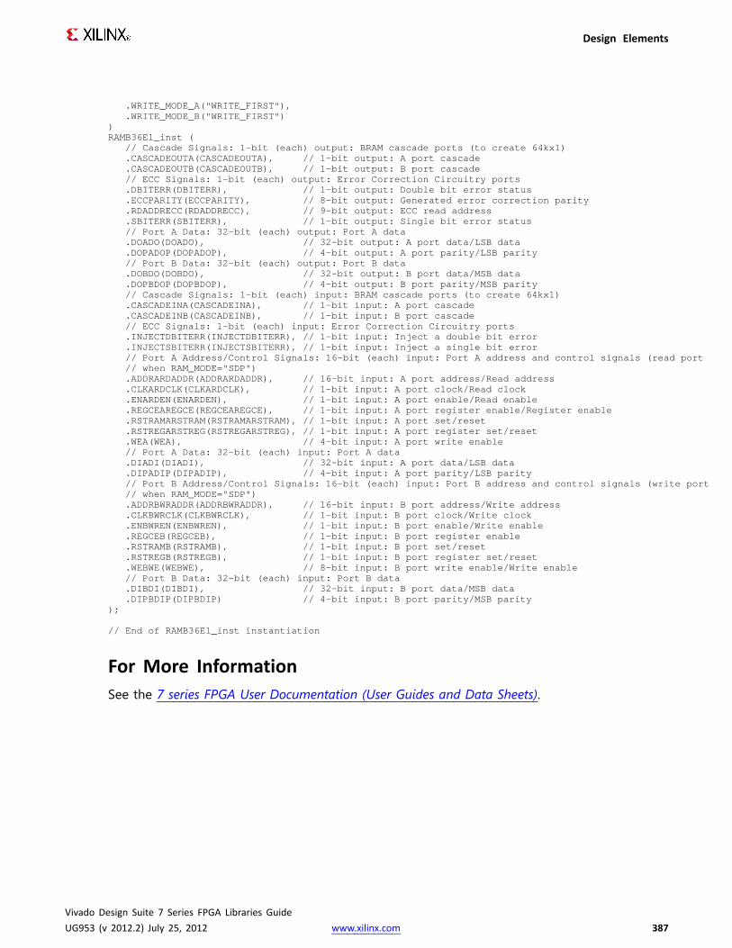
Design Elements
.WRITE_MODE_A("WRITE_FIRST"),
.WRITE_MODE_B("WRITE_FIRST"))RAMB36E1_inst (
// Cascade Signals: 1-bit (each) output: BRAMcascade ports (to create 64kx1).CASCADEOUTA(CASCADEOUTA), // 1-bit output: A port cascade.CASCADEOUTB(CASCADEOUTB), // 1-bit output: B port cascade// ECC Signals: 1-bit (each) output: Error Correction Circuitry ports.DBITERR(DBITERR), // 1-bit output: Double bit error status.ECCPARITY(ECCPARITY), // 8-bit output: Generated error correction parity.RDADDRECC(RDADDRECC), // 9-bit output: ECC read address.SBITERR(SBITERR), // 1-bit output: Single bit error status// Port A Data: 32-bit (each) output: Port A data.DOADO(DOADO), // 32-bit output: A port data/LSB data.DOPADOP(DOPADOP), // 4-bit output: A port parity/LSB parity// Port B Data: 32-bit (each) output: Port B data.DOBDO(DOBDO), // 32-bit output: B port data/MSB data.DOPBDOP(DOPBDOP), // 4-bit output: B port parity/MSB parity// Cascade Signals: 1-bit (each) input: BRAMcascade ports (to create 64kx1).CASCADEINA(CASCADEINA), // 1-bit input: A port cascade.CASCADEINB(CASCADEINB), // 1-bit input: B port cascade// ECC Signals: 1-bit (each) input: Error Correction Circuitry ports.INJECTDBITERR(INJECTDBITERR), // 1-bit input: Inject a double bit error.INJECTSBITERR(INJECTSBITERR), // 1-bit input: Inject a single bit error// Port A Address/Control Signals: 16-bit (each) input: Port A address and control signals (read port// when RAM_MODE="SDP").ADDRARDADDR(ADDRARDADDR), // 16-bit input: A port address/Read address.CLKARDCLK(CLKARDCLK), // 1-bit input: A port clock/Read clock.ENARDEN(ENARDEN), // 1-bit input: A port enable/Read enable.REGCEAREGCE(REGCEAREGCE), // 1-bit input: A port register enable/Register enable.RSTRAMARSTRAM(RSTRAMARSTRAM),// 1-bit input: A port set/reset.RSTREGARSTREG(RSTREGARSTREG),// 1-bit input: A port register set/reset.WEA(WEA), // 4-bit input: A port write enable// Port A Data: 32-bit (each) input: Port A data.DIADI(DIADI), // 32-bit input: A port data/LSB data.DIPADIP(DIPADIP), // 4-bit input: A port parity/LSB parity// Port B Address/Control Signals: 16-bit (each) input: Port B address and control signals (write port// when RAM_MODE="SDP").ADDRBWRADDR(ADDRBWRADDR), // 16-bit input: B port address/Write address.CLKBWRCLK(CLKBWRCLK), // 1-bit input: B port clock/Write clock.ENBWREN(ENBWREN), // 1-bit input: B port enable/Write enable.REGCEB(REGCEB), // 1-bit input: B port register enable.RSTRAMB(RSTRAMB), // 1-bit input: B port set/reset.RSTREGB(RSTREGB), // 1-bit input: B port register set/reset.WEBWE(WEBWE), // 8-bit input: B port write enable/Write enable// Port B Data: 32-bit (each) input: Port B data.DIBDI(DIBDI), // 32-bit input: B port data/MSB data.DIPBDIP(DIPBDIP) // 4-bit input: B port parity/MSB parity
);
// End of RAMB36E1_inst instantiation
For More InformationSee the 7 series FPGA User Documentation (User Guides and Data Sheets).
Vivado Design Suite 7 Series FPGA Libraries GuideUG953 (v 2012.2) July 25, 2012 www.xilinx.com 387

Design Elements
ROM128X1Primitive: 128-Deep by 1-Wide ROM
IntroductionThis design element is a 128-word by 1-bit read-only memory. The data output (O) reflects theword selected by the 7-bit address (A6:A0). The ROM is initialized to a known value duringconfiguration with the INIT=value parameter. The value consists of 32 hexadecimal digits thatare written into the ROM from the most-significant digit A=FH to the least-significant digitA=0H. An error occurs if the INIT=value is not specified.
Logic TableInput Output
I0 I1 I2 I3 O
0 0 0 0 INIT(0)
0 0 0 1 INIT(1)
0 0 1 0 INIT(2)
0 0 1 1 INIT(3)
0 1 0 0 INIT(4)
0 1 0 1 INIT(5)
0 1 1 0 INIT(6)
0 1 1 1 INIT(7)
1 0 0 0 INIT(8)
1 0 0 1 INIT(9)
1 0 1 0 INIT(10)
1 0 1 1 INIT(11)
1 1 0 0 INIT(12)
1 1 0 1 INIT(13)
1 1 1 0 INIT(14)
1 1 1 1 INIT(15)
Vivado Design Suite 7 Series FPGA Libraries GuideUG953 (v 2012.2) July 25, 2012 www.xilinx.com 388
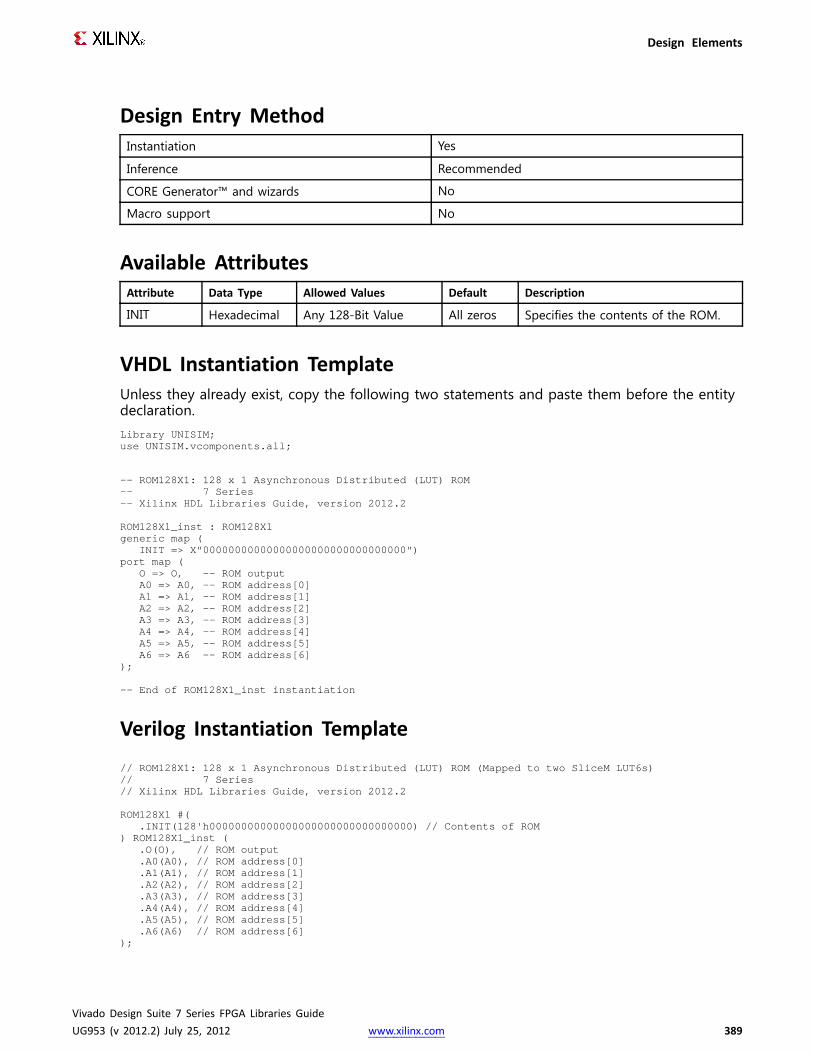
Design Elements
Design Entry MethodInstantiation Yes
Inference Recommended
CORE Generator™ and wizards No
Macro support No
Available AttributesAttribute Data Type Allowed Values Default Description
INIT Hexadecimal Any 128-Bit Value All zeros Specifies the contents of the ROM.
VHDL Instantiation TemplateUnless they already exist, copy the following two statements and paste them before the entitydeclaration.Library UNISIM;use UNISIM.vcomponents.all;
-- ROM128X1: 128 x 1 Asynchronous Distributed (LUT) ROM-- 7 Series-- Xilinx HDL Libraries Guide, version 2012.2
ROM128X1_inst : ROM128X1generic map (
INIT => X"00000000000000000000000000000000")port map (
O => O, -- ROMoutputA0 => A0, -- ROMaddress[0]A1 => A1, -- ROMaddress[1]A2 => A2, -- ROMaddress[2]A3 => A3, -- ROMaddress[3]A4 => A4, -- ROMaddress[4]A5 => A5, -- ROMaddress[5]A6 => A6 -- ROMaddress[6]
);
-- End of ROM128X1_inst instantiation
Verilog Instantiation Template// ROM128X1: 128 x 1 Asynchronous Distributed (LUT) ROM(Mapped to two SliceM LUT6s)// 7 Series// Xilinx HDL Libraries Guide, version 2012.2
ROM128X1 #(.INIT(128'h00000000000000000000000000000000) // Contents of ROM
) ROM128X1_inst (.O(O), // ROMoutput.A0(A0), // ROMaddress[0].A1(A1), // ROMaddress[1].A2(A2), // ROMaddress[2].A3(A3), // ROMaddress[3].A4(A4), // ROMaddress[4].A5(A5), // ROMaddress[5].A6(A6) // ROMaddress[6]
);
Vivado Design Suite 7 Series FPGA Libraries GuideUG953 (v 2012.2) July 25, 2012 www.xilinx.com 389

Design Elements
// End of ROM128X1_inst instantiation
For More InformationSee the 7 series FPGA User Documentation (User Guides and Data Sheets).
Vivado Design Suite 7 Series FPGA Libraries GuideUG953 (v 2012.2) July 25, 2012 www.xilinx.com 390

Design Elements
ROM256X1Primitive: 256-Deep by 1-Wide ROM
IntroductionThis design element is a 256-word by 1-bit read-only memory. The data output (O) reflects theword selected by the 8-bit address (A7:A0). The ROM is initialized to a known value duringconfiguration with the INIT=value parameter. The value consists of 64 hexadecimal digitsthat are written into the ROM from the most-significant digit A=FH to the least-significantdigit A=0H.
An error occurs if the INIT=value is not specified.
Logic TableInput Output
I0 I1 I2 I3 O
0 0 0 0 INIT(0)
0 0 0 1 INIT(1)
0 0 1 0 INIT(2)
0 0 1 1 INIT(3)
0 1 0 0 INIT(4)
0 1 0 1 INIT(5)
0 1 1 0 INIT(6)
0 1 1 1 INIT(7)
1 0 0 0 INIT(8)
1 0 0 1 INIT(9)
1 0 1 0 INIT(10)
1 0 1 1 INIT(11)
1 1 0 0 INIT(12)
1 1 0 1 INIT(13)
Vivado Design Suite 7 Series FPGA Libraries GuideUG953 (v 2012.2) July 25, 2012 www.xilinx.com 391

Design Elements
Input Output
I0 I1 I2 I3 O
1 1 1 0 INIT(14)
1 1 1 1 INIT(15)
Design Entry MethodInstantiation Yes
Inference Recommended
CORE Generator™ and wizards No
Macro support No
Available AttributesAttribute Data Type Allowed Values Default Description
INIT Hexadecimal Any 256-Bit Value All zeros Specifies the contents of theROM.
VHDL Instantiation TemplateUnless they already exist, copy the following two statements and paste them before the entitydeclaration.Library UNISIM;use UNISIM.vcomponents.all;
-- ROM256X1: 256 x 1 Asynchronous Distributed (LUT) ROM-- 7 Series-- Xilinx HDL Libraries Guide, version 2012.2
ROM256X1_inst : ROM256X1generic map (
INIT => X"0000000000000000000000000000000000000000000000000000000000000000")port map (
O => O, -- ROMoutputA0 => A0, -- ROMaddress[0]A1 => A1, -- ROMaddress[1]A2 => A2, -- ROMaddress[2]A3 => A3, -- ROMaddress[3]A4 => A4, -- ROMaddress[4]A5 => A5, -- ROMaddress[5]A6 => A6, -- ROMaddress[6]A7 => A7 -- ROMaddress[7]
);
-- End of ROM256X1_inst instantiation
Vivado Design Suite 7 Series FPGA Libraries GuideUG953 (v 2012.2) July 25, 2012 www.xilinx.com 392
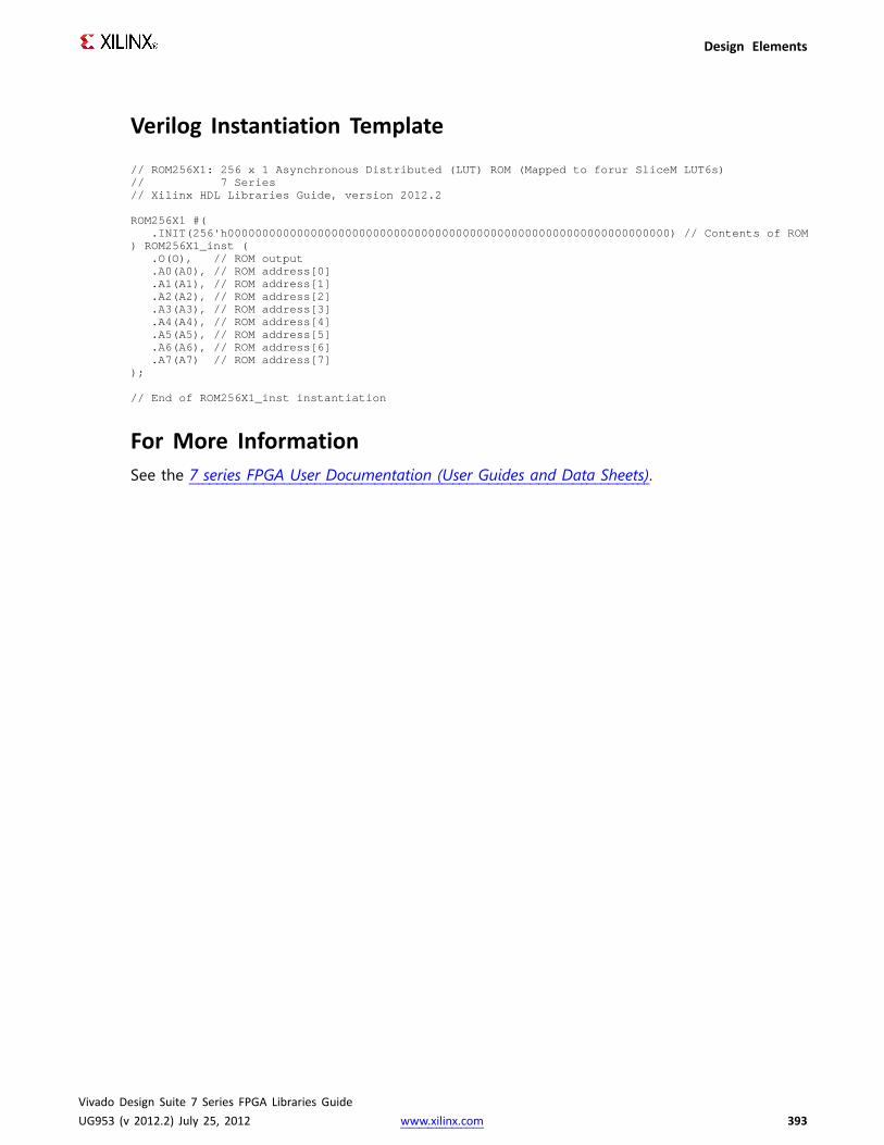
Design Elements
Verilog Instantiation Template
// ROM256X1: 256 x 1 Asynchronous Distributed (LUT) ROM(Mapped to forur SliceM LUT6s)// 7 Series// Xilinx HDL Libraries Guide, version 2012.2
ROM256X1 #(.INIT(256'h0000000000000000000000000000000000000000000000000000000000000000) // Contents of ROM
) ROM256X1_inst (.O(O), // ROMoutput.A0(A0), // ROMaddress[0].A1(A1), // ROMaddress[1].A2(A2), // ROMaddress[2].A3(A3), // ROMaddress[3].A4(A4), // ROMaddress[4].A5(A5), // ROMaddress[5].A6(A6), // ROMaddress[6].A7(A7) // ROMaddress[7]
);
// End of ROM256X1_inst instantiation
For More InformationSee the 7 series FPGA User Documentation (User Guides and Data Sheets).
Vivado Design Suite 7 Series FPGA Libraries GuideUG953 (v 2012.2) July 25, 2012 www.xilinx.com 393

Design Elements
ROM32X1Primitive: 32-Deep by 1-Wide ROM
IntroductionThis design element is a 32-word by 1-bit read-only memory. The data output (O) reflects theword selected by the 5-bit address (A4:A0). The ROM is initialized to a known value duringconfiguration with the INIT=value parameter. The value consists of eight hexadecimal digitsthat are written into the ROM from the most-significant digit A=1FH to the least-significantdigit A=00H.
For example, the INIT=10A78F39 parameter produces the data stream: 0001 0000 1010 01111000 1111 0011 1001. An error occurs if the INIT=value is not specified.
Logic TableInput Output
I0 I1 I2 I3 O
0 0 0 0 INIT(0)
0 0 0 1 INIT(1)
0 0 1 0 INIT(2)
0 0 1 1 INIT(3)
0 1 0 0 INIT(4)
0 1 0 1 INIT(5)
0 1 1 0 INIT(6)
0 1 1 1 INIT(7)
1 0 0 0 INIT(8)
1 0 0 1 INIT(9)
1 0 1 0 INIT(10)
1 0 1 1 INIT(11)
1 1 0 0 INIT(12)
1 1 0 1 INIT(13)
1 1 1 0 INIT(14)
1 1 1 1 INIT(15)
Vivado Design Suite 7 Series FPGA Libraries GuideUG953 (v 2012.2) July 25, 2012 www.xilinx.com 394

Design Elements
Design Entry MethodInstantiation Yes
Inference Recommended
CORE Generator™ and wizards No
Macro support No
Available AttributesAttribute Type Allowed Values Default Description
INIT Hexadecimal Any 32-Bit Value All zeros Specifies the contents of theROM.
VHDL Instantiation TemplateUnless they already exist, copy the following two statements and paste them before the entitydeclaration.Library UNISIM;use UNISIM.vcomponents.all;
-- ROM32X1: 32 x 1 Asynchronous Distributed (LUT) ROM-- 7 Series-- Xilinx HDL Libraries Guide, version 2012.2
ROM32X1_inst : ROM32X1generic map (
INIT => X"00000000")port map (
O => O, -- ROMoutputA0 => A0, -- ROMaddress[0]A1 => A1, -- ROMaddress[1]A2 => A2, -- ROMaddress[2]A3 => A3, -- ROMaddress[3]A4 => A4 -- ROMaddress[4]
);-- End of ROM32X1_inst instantiation
Verilog Instantiation Template
// ROM32X1: 32 x 1 Asynchronous Distributed (LUT) ROM(Mapped to a SliceM LUT6)// 7 Series// Xilinx HDL Libraries Guide, version 2012.2
ROM32X1#(.INIT(32'h00000000) // Contents of ROM
) ROM32X1_inst (.O(O), // ROMoutput.A0(A0), // ROMaddress[0].A1(A1), // ROMaddress[1].A2(A2), // ROMaddress[2].A3(A3), // ROMaddress[3].A4(A4) // ROMaddress[4]
);
// End of ROM32X1_inst instantiation
Vivado Design Suite 7 Series FPGA Libraries GuideUG953 (v 2012.2) July 25, 2012 www.xilinx.com 395

Design Elements
For More InformationSee the 7 series FPGA User Documentation (User Guides and Data Sheets).
Vivado Design Suite 7 Series FPGA Libraries GuideUG953 (v 2012.2) July 25, 2012 www.xilinx.com 396

Design Elements
ROM64X1Primitive: 64-Deep by 1-Wide ROM
IntroductionThis design element is a 64-word by 1-bit read-only memory. The data output (O) reflects theword selected by the 6-bit address (A5:A0). The ROM is initialized to a known value duringconfiguration with the INIT=value parameter. The value consists of 16 hexadecimal digits thatare written into the ROM from the most-significant digit A=FH to the least-significant digitA=0H. An error occurs if the INIT=value is not specified.
Logic TableInput Output
I0 I1 I2 I3 O
0 0 0 0 INIT(0)
0 0 0 1 INIT(1)
0 0 1 0 INIT(2)
0 0 1 1 INIT(3)
0 1 0 0 INIT(4)
0 1 0 1 INIT(5)
0 1 1 0 INIT(6)
0 1 1 1 INIT(7)
1 0 0 0 INIT(8)
1 0 0 1 INIT(9)
1 0 1 0 INIT(10)
1 0 1 1 INIT(11)
1 1 0 0 INIT(12)
1 1 0 1 INIT(13)
1 1 1 0 INIT(14)
1 1 1 1 INIT(15)
Vivado Design Suite 7 Series FPGA Libraries GuideUG953 (v 2012.2) July 25, 2012 www.xilinx.com 397

Design Elements
Design Entry MethodInstantiation Yes
Inference Recommended
CORE Generator™ and wizards No
Macro support No
Available AttributesAttribute Data Type Allowed Values Default Description
INIT Hexadecimal Any 64-Bit Value All zeros Specifies the contents of the ROM.
VHDL Instantiation TemplateUnless they already exist, copy the following two statements and paste them before the entitydeclaration.Library UNISIM;use UNISIM.vcomponents.all;
-- ROM64X1: 64 x 1 Asynchronous Distributed (LUT) ROM-- 7 Series-- Xilinx HDL Libraries Guide, version 2012.2
ROM64X1_inst : ROM64X1generic map (
INIT => X"0000000000000000")port map (
O => O, -- ROMoutputA0 => A0, -- ROMaddress[0]A1 => A1, -- ROMaddress[1]A2 => A2, -- ROMaddress[2]A3 => A3, -- ROMaddress[3]A4 => A4, -- ROMaddress[4]A5 => A5 -- ROMaddress[5]
);
-- End of ROM64X1_inst instantiation
Verilog Instantiation Template// ROM64X1: 64 x 1 Asynchronous Distributed (LUT) ROM(Mapped to a SliceM LUT6)// 7 Series// Xilinx HDL Libraries Guide, version 2012.2
ROM64X1#(.INIT(64'h0000000000000000) // Contents of ROM
) ROM64X1_inst (.O(O), // ROMoutput.A0(A0), // ROMaddress[0].A1(A1), // ROMaddress[1].A2(A2), // ROMaddress[2].A3(A3), // ROMaddress[3].A4(A4), // ROMaddress[4].A5(A5) // ROMaddress[5]
);
// End of ROM64X1_inst instantiation
Vivado Design Suite 7 Series FPGA Libraries GuideUG953 (v 2012.2) July 25, 2012 www.xilinx.com 398

Design Elements
For More InformationSee the 7 series FPGA User Documentation (User Guides and Data Sheets).
Vivado Design Suite 7 Series FPGA Libraries GuideUG953 (v 2012.2) July 25, 2012 www.xilinx.com 399

Design Elements
SRL16EPrimitive: 16-Bit Shift Register Look-Up Table (LUT) with Clock Enable
IntroductionThis design element is a shift register look-up table (LUT). The inputs A3, A2, A1, and A0select the output length of the shift register.
The shift register can be of a fixed, static length or it can be dynamically adjusted.• To create a fixed-length shift register: Drive the A3 through A0 inputs with static
values. The length of the shift register can vary from 1 bit to 16 bits, as determinedby the following formula: Length = (8 x A3) +(4 x A2) + (2 x A1) + A0 +1 If A3, A2,A1, and A0 are all zeros (0000), the shift register is one bit long. If they are all ones(1111), it is 16 bits long.
• To change the length of the shift register dynamically: Change the values driving theA3 through A0 inputs. For example, if A2, A1, and A0 are all ones (111) and A3 togglesbetween a one (1) and a zero (0), the length of the shift register changes from 16 bits to8 bits. Internally, the length of the shift register is always 16 bits and the input lines A3through A0 select which of the 16 bits reach the output.
The shift register LUT contents are initialized by assigning a four-digit hexadecimal numberto an INIT attribute. The first, or the left-most, hexadecimal digit is the most significant bit.If an INIT value is not specified, it defaults to a value of four zeros (0000) so that the shiftregister LUT is cleared during configuration.
When CE is High, the data (D) is loaded into the first bit of the shift register during theLow-to-High clock (CLK) transition. During subsequent Low-to-High clock transitions, when CEis High, data shifts to the next highest bit position as new data is loaded. The data appears onthe Q output when the shift register length determined by the address inputs is reached. WhenCE is Low, the register ignores clock transitions.
Logic TableInputs Output
Am CE CLK D Q
Am 0 X X Q(Am)
Am 1 ↑ D Q(Am - 1)
m= 0, 1, 2, 3
Vivado Design Suite 7 Series FPGA Libraries GuideUG953 (v 2012.2) July 25, 2012 www.xilinx.com 400

Design Elements
Port DescriptionsPort Direction Width Function
Q Output 1 Shift register data output
D Input 1 Shift register data input
CLK Input 1 Clock
CE Input 1 Active high clock enable
A0 Input 1 Select[0] input
A1 Input 1 Select[1] input
A2 Input 1 Select[2] input
A3 Input 1 Select[3] input
Design Entry MethodInstantiation Yes
Inference Recommended
CORE Generator™ and wizards No
Macro support No
Available AttributesAttribute Data Type Allowed Values Default Description
INIT Hexa-decimal
Any 16-Bit Value All zeros Sets the initial value of content and output ofshift register after configuration.
VHDL Instantiation TemplateUnless they already exist, copy the following two statements and paste them before the entitydeclaration.Library UNISIM;use UNISIM.vcomponents.all;
-- SRL16E: 16-bit shift register LUT with clock enable operating on posedge of clock (Mapped to SliceM LUT6)-- 7 Series-- Xilinx HDL Libraries Guide, version 2012.2
SRL16E_inst : SRL16Egeneric map (
INIT => X"0000")port map (
Q => Q, -- SRL data outputA0 => A0, -- Select[0] inputA1 => A1, -- Select[1] inputA2 => A2, -- Select[2] inputA3 => A3, -- Select[3] inputCE => CE, -- Clock enable inputCLK => CLK, -- Clock inputD => D -- SRL data input
);
Vivado Design Suite 7 Series FPGA Libraries GuideUG953 (v 2012.2) July 25, 2012 www.xilinx.com 401
Design Elements
-- End of SRL16E_inst instantiation
Verilog Instantiation Template
// SRL16E: 16-bit shift register LUT with clock enable operating on posedge of clock (Mapped to a SliceM LUT6)// 7 Series// Xilinx HDL Libraries Guide, version 2012.2
SRL16E #(.INIT(16'h0000) // Initial Value of Shift Register
) SRL16E_inst (.Q(Q), // SRL data output.A0(A0), // Select[0] input.A1(A1), // Select[1] input.A2(A2), // Select[2] input.A3(A3), // Select[3] input.CE(CE), // Clock enable input.CLK(CLK), // Clock input.D(D) // SRL data input
);
// End of SRL16E_inst instantiation
For More InformationSee the 7 series FPGA User Documentation (User Guides and Data Sheets).
Vivado Design Suite 7 Series FPGA Libraries GuideUG953 (v 2012.2) July 25, 2012 www.xilinx.com 402

Design Elements
SRLC32EPrimitive: 32 Clock Cycle, Variable Length Shift Register Look-Up Table (LUT)with Clock Enable
IntroductionThis design element is a variable length, 1 to 32 clock cycle shift register implemented within asingle look-up table (LUT). The shift register can be of a fixed length, static length, or it canbe dynamically adjusted by changing the address lines to the component. This element alsofeatures an active-high clock enable and a cascading feature in which multiple SRLC32Es can becascaded in order to create greater shift lengths.
Port DescriptionsPort Direction Width Function
Q Output 1 Shift register data output
Q31 Output 1 Shift register cascaded output (connect to theD input of a subsequent SRLC32E)
D Input 1 Shift register data input
CLK Input 1 Clock
CE Input 1 Active high clock enable
A Input 5 Dynamic depth selection of the SRL
A=00000 ==> 1-bit shift length
A=11111 ==> 32-bit shift length
Vivado Design Suite 7 Series FPGA Libraries GuideUG953 (v 2012.2) July 25, 2012 www.xilinx.com 403

Design Elements
Design Entry MethodInstantiation Yes
Inference Recommended
CORE Generator™ and wizards No
Macro support No
If instantiated, the following connections should be made to this component:• Connect the CLK input to the desired clock source, the D input to the data source
to be shifted/stored and the Q output to either an FDCE or an FDRE input or otherappropriate data destination.
• The CE clock enable pin can be connected to a clock enable signal in the design or elsetied to a logic one if not used.
• The 5-bit A bus can either be tied to a static value between 0 and 31 to signify a fixed1 to 32 bit static shift length, or else it can be tied to the appropriate logic to enablea varying shift depth anywhere between 1 and 32 bits.
• If you want to create a longer shift length than 32, connect the Q31 output pin to the Dinput pin of a subsequent SRLC32E to cascade and create larger shift registers.
• It is not valid to connect the Q31 output to anything other than another SRLC32E.• The selectable Q output is still available in the cascaded mode, if needed.• An optional INIT attribute consisting of a 32-bit Hexadecimal value can be specified
to indicate the initial shift pattern of the shift register.• (INIT[0] will be the first value shifted out.)
Available AttributesAttribute Type Allowed Values Default Description
INIT Hexa-decimal
Any 32-Bit Value All zeros Specifies the initial shift pattern of theSRLC32E.
VHDL Instantiation TemplateUnless they already exist, copy the following two statements and paste them before the entitydeclaration.Library UNISIM;use UNISIM.vcomponents.all;
-- SRLC32E: 32-bit variable length shift register LUT-- with clock enable (Mapped to a SliceM LUT6)-- 7 Series-- Xilinx HDL Libraries Guide, version 2012.2
SRLC32E_inst : SRLC32Egeneric map (
INIT => X"00000000")port map (
Q => Q, -- SRL data outputQ31 => Q31, -- SRL cascade output pinA => A, -- 5-bit shift depth select inputCE => CE, -- Clock enable inputCLK => CLK, -- Clock input
Vivado Design Suite 7 Series FPGA Libraries GuideUG953 (v 2012.2) July 25, 2012 www.xilinx.com 404

Design Elements
D => D -- SRL data input);
-- End of SRLC32E_inst instantiation
Verilog Instantiation Template
// SRLC32E: 32-bit variable length cascadable shift register LUT (Mapped to a SliceM LUT6)// with clock enable// 7 Series// Xilinx HDL Libraries Guide, version 2012.2
SRLC32E #(.INIT(32'h00000000) // Initial Value of Shift Register
) SRLC32E_inst (.Q(Q), // SRL data output.Q31(Q31), // SRL cascade output pin.A(A), // 5-bit shift depth select input.CE(CE), // Clock enable input.CLK(CLK), // Clock input.D(D) // SRL data input
);
// End of SRLC32E_inst instantiation
For More InformationSee the 7 series FPGA User Documentation (User Guides and Data Sheets).
Vivado Design Suite 7 Series FPGA Libraries GuideUG953 (v 2012.2) July 25, 2012 www.xilinx.com 405

Design Elements
STARTUPE2Primitive: STARTUP Block
IntroductionThis design element is used to interface device pins and logic to the global asynchronousset/reset (GSR) signal, the global 3-state (GTS) dedicated routing or the internal configurationsignals or a few of the dedicated configuration pins.
Port DescriptionsPort Type Width Function
CFGCLK Output 1 Configuration main clock output
CFGMCLK Output 1 Configuration internal oscillator clock output
CLK Input 1 User start-up clock input
EOS Output 1 Active high output signal indicating the End Of Startup.
GSR Input 1 Global Set/Reset input (GSR cannot be used for the port name)
GTS Input 1 Global 3-state input (GTS cannot be used for the port name)
KEYCLEARB Input 1 Clear AES Decrypter Key input from Battery-Backed RAM(BBRAM)
PACK Input 1 PROGRAM acknowledge input
PREQ Output 1 PROGRAM request to fabric output
USRCCLKO Input 1 User CCLK input
USRCCLKTS Input 1 User CCLK 3-state enable input
USRDONEO Input 1 User DONE pin output control
USRDONETS Input 1 User DONE 3-state enable output
Vivado Design Suite 7 Series FPGA Libraries GuideUG953 (v 2012.2) July 25, 2012 www.xilinx.com 406

Design Elements
Design Entry MethodInstantiation Recommended
Inference No
CORE Generator™ and wizards No
Macro support No
Available AttributesAttribute Type Allowed Values Default Description
PROG_USR STRING "FALSE", "TRUE" "FALSE" Activate program event securityfeature. Requires encryptedbitstreams.
SIM_CCLK_FREQ
FLOAT(nS) 0.0 to 10.0 0.0 Set the Configuration ClockFrequency(ns) for simulation.
VHDL Instantiation TemplateUnless they already exist, copy the following two statements and paste them before the entitydeclaration.Library UNISIM;use UNISIM.vcomponents.all;
-- STARTUPE2: STARTUPBlock-- 7 Series-- Xilinx HDL Libraries Guide, version 2012.2
STARTUPE2_inst : STARTUPE2generic map (
PROG_USR=> "FALSE", -- Activate program event security feature. Requires encrypted bitstreams.SIM_CCLK_FREQ=> 0.0 -- Set the Configuration Clock Frequency(ns) for simulation.
)port map (
CFGCLK=> CFGCLK, -- 1-bit output: Configuration main clock outputCFGMCLK=> CFGMCLK, -- 1-bit output: Configuration internal oscillator clock outputEOS => EOS, -- 1-bit output: Active high output signal indicating the End Of Startup.PREQ=> PREQ, -- 1-bit output: PROGRAMrequest to fabric outputCLK => CLK, -- 1-bit input: User start-up clock inputGSR => GSR, -- 1-bit input: Global Set/Reset input (GSR cannot be used for the port name)GTS => GTS, -- 1-bit input: Global 3-state input (GTS cannot be used for the port name)KEYCLEARB=> KEYCLEARB, -- 1-bit input: Clear AES Decrypter Key input from Battery-Backed RAM (BBRAM)PACK => PACK, -- 1-bit input: PROGRAMacknowledge inputUSRCCLKO=> USRCCLKO, -- 1-bit input: User CCLK inputUSRCCLKTS=> USRCCLKTS, -- 1-bit input: User CCLK 3-state enable inputUSRDONEO=> USRDONEO, -- 1-bit input: User DONEpin output controlUSRDONETS=> USRDONETS -- 1-bit input: User DONE3-state enable output
);
-- End of STARTUPE2_inst instantiation
Vivado Design Suite 7 Series FPGA Libraries GuideUG953 (v 2012.2) July 25, 2012 www.xilinx.com 407
Design Elements
Verilog Instantiation Template
// STARTUPE2: STARTUPBlock// 7 Series// Xilinx HDL Libraries Guide, version 2012.2
STARTUPE2#(.PROG_USR("FALSE"), // Activate program event security feature. Requires encrypted bitstreams..SIM_CCLK_FREQ(0.0) // Set the Configuration Clock Frequency(ns) for simulation.
)STARTUPE2_inst (
.CFGCLK(CFGCLK), // 1-bit output: Configuration main clock output
.CFGMCLK(CFGMCLK), // 1-bit output: Configuration internal oscillator clock output
.EOS(EOS), // 1-bit output: Active high output signal indicating the End Of Startup.
.PREQ(PREQ), // 1-bit output: PROGRAMrequest to fabric output
.CLK(CLK), // 1-bit input: User start-up clock input
.GSR(GSR), // 1-bit input: Global Set/Reset input (GSR cannot be used for the port name)
.GTS(GTS), // 1-bit input: Global 3-state input (GTS cannot be used for the port name)
.KEYCLEARB(KEYCLEARB), // 1-bit input: Clear AES Decrypter Key input from Battery-Backed RAM (BBRAM)
.PACK(PACK), // 1-bit input: PROGRAMacknowledge input
.USRCCLKO(USRCCLKO), // 1-bit input: User CCLK input
.USRCCLKTS(USRCCLKTS), // 1-bit input: User CCLK 3-state enable input
.USRDONEO(USRDONEO), // 1-bit input: User DONEpin output control
.USRDONETS(USRDONETS) // 1-bit input: User DONE3-state enable output);
// End of STARTUPE2_inst instantiation
For More InformationSee the 7 series FPGA User Documentation (User Guides and Data Sheets).
Vivado Design Suite 7 Series FPGA Libraries GuideUG953 (v 2012.2) July 25, 2012 www.xilinx.com 408
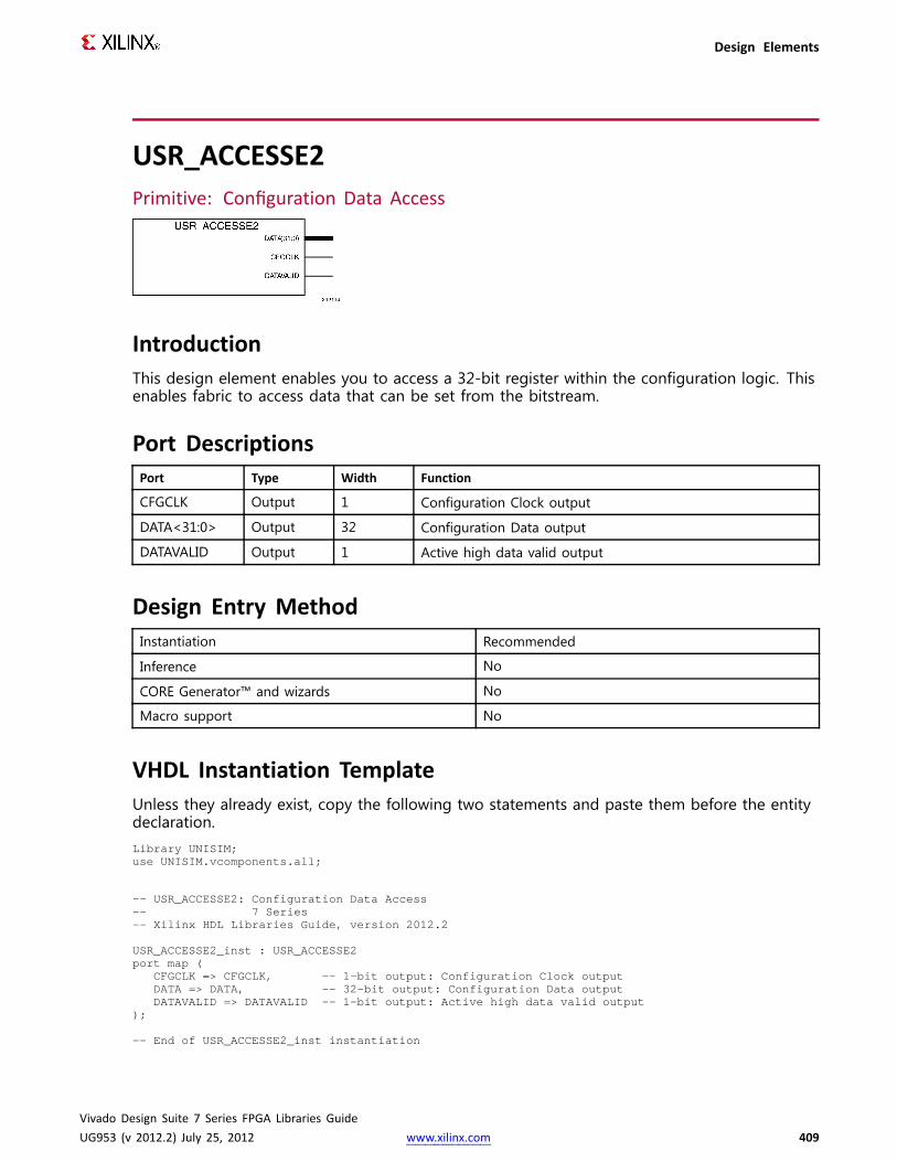
Design Elements
USR_ACCESSE2Primitive: Configuration Data Access
IntroductionThis design element enables you to access a 32-bit register within the configuration logic. Thisenables fabric to access data that can be set from the bitstream.
Port DescriptionsPort Type Width Function
CFGCLK Output 1 Configuration Clock output
DATA<31:0> Output 32 Configuration Data output
DATAVALID Output 1 Active high data valid output
Design Entry MethodInstantiation Recommended
Inference No
CORE Generator™ and wizards No
Macro support No
VHDL Instantiation TemplateUnless they already exist, copy the following two statements and paste them before the entitydeclaration.Library UNISIM;use UNISIM.vcomponents.all;
-- USR_ACCESSE2:Configuration Data Access-- 7 Series-- Xilinx HDL Libraries Guide, version 2012.2
USR_ACCESSE2_inst : USR_ACCESSE2port map (
CFGCLK=> CFGCLK, -- 1-bit output: Configuration Clock outputDATA => DATA, -- 32-bit output: Configuration Data outputDATAVALID => DATAVALID -- 1-bit output: Active high data valid output
);
-- End of USR_ACCESSE2_inst instantiation
Vivado Design Suite 7 Series FPGA Libraries GuideUG953 (v 2012.2) July 25, 2012 www.xilinx.com 409

Design Elements
Verilog Instantiation Template
// USR_ACCESSE2:Configuration Data Access// 7 Series// Xilinx HDL Libraries Guide, version 2012.2
USR_ACCESSE2USR_ACCESSE2_inst (.CFGCLK(CFGCLK), // 1-bit output: Configuration Clock output.DATA(DATA), // 32-bit output: Configuration Data output.DATAVALID(DATAVALID) // 1-bit output: Active high data valid output
);
// End of USR_ACCESSE2_inst instantiation
For More Information• See the 7 series FPGA SelectIO Resources User Guide (UG471).
• See the 7 series FPGA User Documentation (User Guides and Data Sheets).
Vivado Design Suite 7 Series FPGA Libraries GuideUG953 (v 2012.2) July 25, 2012 www.xilinx.com 410
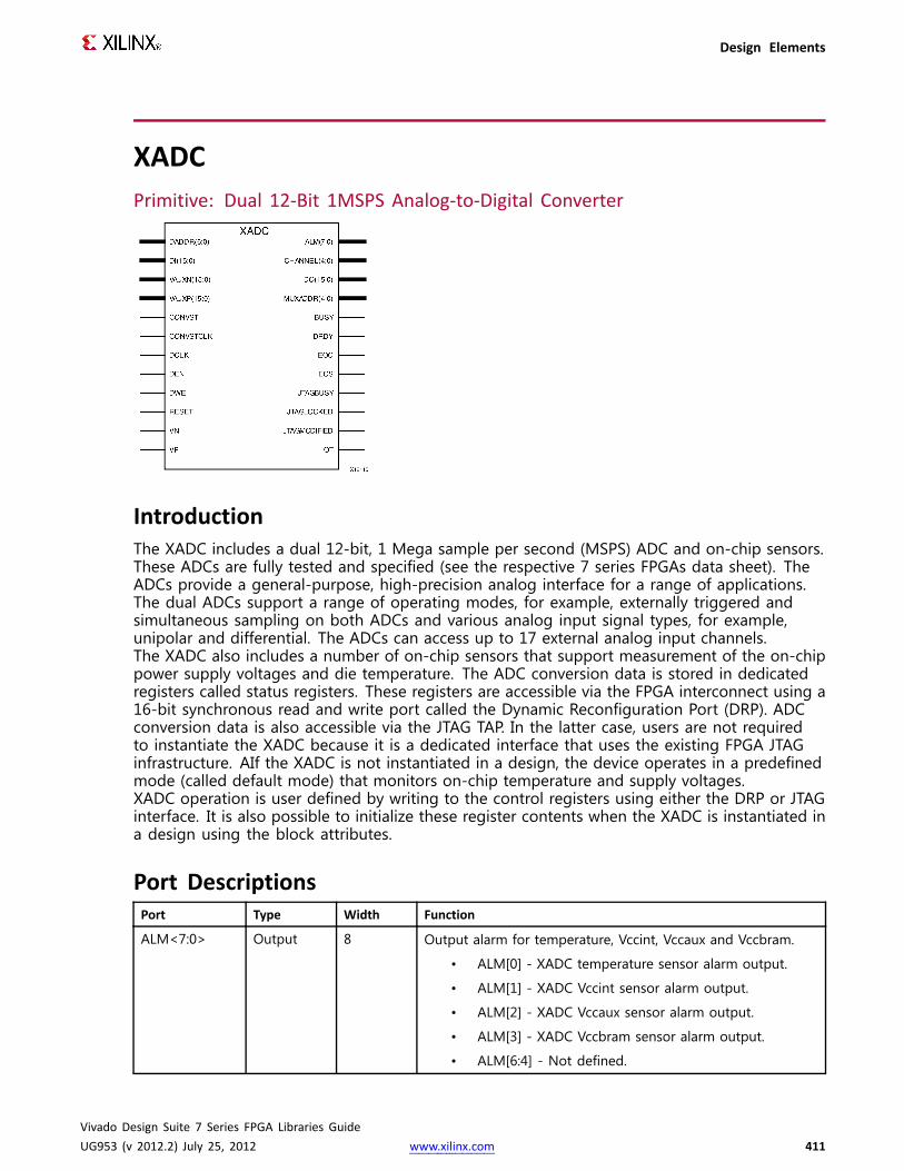
Design Elements
XADCPrimitive: Dual 12-Bit 1MSPS Analog-to-Digital Converter
IntroductionThe XADC includes a dual 12-bit, 1 Mega sample per second (MSPS) ADC and on-chip sensors.These ADCs are fully tested and specified (see the respective 7 series FPGAs data sheet). TheADCs provide a general-purpose, high-precision analog interface for a range of applications.The dual ADCs support a range of operating modes, for example, externally triggered andsimultaneous sampling on both ADCs and various analog input signal types, for example,unipolar and differential. The ADCs can access up to 17 external analog input channels.The XADC also includes a number of on-chip sensors that support measurement of the on-chippower supply voltages and die temperature. The ADC conversion data is stored in dedicatedregisters called status registers. These registers are accessible via the FPGA interconnect using a16-bit synchronous read and write port called the Dynamic Reconfiguration Port (DRP). ADCconversion data is also accessible via the JTAG TAP. In the latter case, users are not requiredto instantiate the XADC because it is a dedicated interface that uses the existing FPGA JTAGinfrastructure. AIf the XADC is not instantiated in a design, the device operates in a predefinedmode (called default mode) that monitors on-chip temperature and supply voltages.XADC operation is user defined by writing to the control registers using either the DRP or JTAGinterface. It is also possible to initialize these register contents when the XADC is instantiated ina design using the block attributes.
Port DescriptionsPort Type Width Function
ALM<7:0> Output 8 Output alarm for temperature, Vccint, Vccaux and Vccbram.
• ALM[0] - XADC temperature sensor alarm output.
• ALM[1] - XADC Vccint sensor alarm output.
• ALM[2] - XADC Vccaux sensor alarm output.
• ALM[3] - XADC Vccbram sensor alarm output.
• ALM[6:4] - Not defined.
Vivado Design Suite 7 Series FPGA Libraries GuideUG953 (v 2012.2) July 25, 2012 www.xilinx.com 411

Design Elements
Port Type Width Function
BUSY Output 1 ADC busy signal. This signal transitions High during an ADCconversion. This signal also transitions High for an extendedperiod during an ADC or sensor calibration.
CHANNEL<4:0> Output 5 Channel selection outputs. The ADC input MUX channelselection for the current ADC conversion is placed on theseoutputs at the end of an ADC conversion.
CONVST Input 1 Convert start input. This input controls the sampling instanton the ADC(s) input and is only used in event mode timing.This input comes from the general-purpose interconnect inthe FPGA logic.
CONVSTCLK Input 1 Convert start clock input. This input is connected to a clocknet. Like CONVST, this input controls the sampling instant onthe ADC(s) inputs and is only used in event mode timing.This input comes from the local clock distribution network inthe FPGA logic. Thus, for the best control over the samplinginstant (delay and jitter), a global clock input can be used asthe CONVST source.
DADDR<6:0> Input 7 Address bus for the dynamic reconfiguration port.
DCLK Input 1 Clock input for the dynamic reconfiguration port.
DEN Input 1 Enable signal for the dynamic reconfiguration port.
DI<15:0> Input 16 Input data bus for the dynamic reconfiguration port.
DO<15:0> Output 16 Output data bus for dynamic reconfiguration port.
DRDY Output 1 Data ready signal for the dynamic reconfiguration port.
DWE Input 1 Write enable for the dynamic reconfiguration port.
EOC Output 1 End of Conversion signal. This signal transitions to an activeHigh at the end of an ADC conversion when the measurementis written to the status registers.
EOS Output 1 End of Sequence. This signal transitions to active High whenthe measurement data from the last channel in an automaticchannel sequence is written to the status registers.
JTAGBUSY Output 1 Used to indicate that a JTAG DRP transaction is in progress.
JTAGLOCKED Output 1 Indicates that a DRP port lock request has been made by theJTAG interface. This signal is also used to indicate that the DRPis ready for access (when Low).
JTAGMODIFIED Output 1 Used to indicate that a JTAG Write to the DRP has occurred.
MUXADDR<4:0> Output 5 These outputs are used in external multiplexer mode. Theyindicate the address of the next channel in a sequence to beconverted. They provide the channel address for an externalmultiplexer.
OT Output 1 Over-Temperature alarm
RESET Input 1 Reset signal for the XADC control logic.
VAUXN<15:0> Input 16 N-side auxiliary analog input
VAUXP<15:0> Input 16 P-side auxiliary analog input
VN Input 1 N-side analog input
VP Input 1 P-side analog input
Vivado Design Suite 7 Series FPGA Libraries GuideUG953 (v 2012.2) July 25, 2012 www.xilinx.com 412
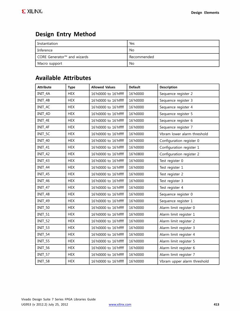
Design Elements
Design Entry MethodInstantiation Yes
Inference No
CORE Generator™ and wizards Recommended
Macro support No
Available AttributesAttribute Type Allowed Values Default Description
INIT_4A HEX 16'h0000 to 16'hffff 16'h0000 Sequence register 2
INIT_4B HEX 16'h0000 to 16'hffff 16'h0000 Sequence register 3
INIT_4C HEX 16'h0000 to 16'hffff 16'h0000 Sequence register 4
INIT_4D HEX 16'h0000 to 16'hffff 16'h0000 Sequence register 5
INIT_4E HEX 16'h0000 to 16'hffff 16'h0000 Sequence register 6
INIT_4F HEX 16'h0000 to 16'hffff 16'h0000 Sequence register 7
INIT_5C HEX 16'h0000 to 16'hffff 16'h0000 Vbram lower alarm threshold
INIT_40 HEX 16'h0000 to 16'hffff 16'h0000 Configuration register 0
INIT_41 HEX 16'h0000 to 16'hffff 16'h0000 Configuration register 1
INIT_42 HEX 16'h0000 to 16'hffff 16'h0800 Configuration register 2
INIT_43 HEX 16'h0000 to 16'hffff 16'h0000 Test register 0
INIT_44 HEX 16'h0000 to 16'hffff 16'h0000 Test register 1
INIT_45 HEX 16'h0000 to 16'hffff 16'h0000 Test register 2
INIT_46 HEX 16'h0000 to 16'hffff 16'h0000 Test register 3
INIT_47 HEX 16'h0000 to 16'hffff 16'h0000 Test register 4
INIT_48 HEX 16'h0000 to 16'hffff 16'h0000 Sequence register 0
INIT_49 HEX 16'h0000 to 16'hffff 16'h0000 Sequence register 1
INIT_50 HEX 16'h0000 to 16'hffff 16'h0000 Alarm limit register 0
INIT_51 HEX 16'h0000 to 16'hffff 16'h0000 Alarm limit register 1
INIT_52 HEX 16'h0000 to 16'hffff 16'h0000 Alarm limit register 2
INIT_53 HEX 16'h0000 to 16'hffff 16'h0000 Alarm limit register 3
INIT_54 HEX 16'h0000 to 16'hffff 16'h0000 Alarm limit register 4
INIT_55 HEX 16'h0000 to 16'hffff 16'h0000 Alarm limit register 5
INIT_56 HEX 16'h0000 to 16'hffff 16'h0000 Alarm limit register 6
INIT_57 HEX 16'h0000 to 16'hffff 16'h0000 Alarm limit register 7
INIT_58 HEX 16'h0000 to 16'hffff 16'h0000 Vbram upper alarm threshold
Vivado Design Suite 7 Series FPGA Libraries GuideUG953 (v 2012.2) July 25, 2012 www.xilinx.com 413
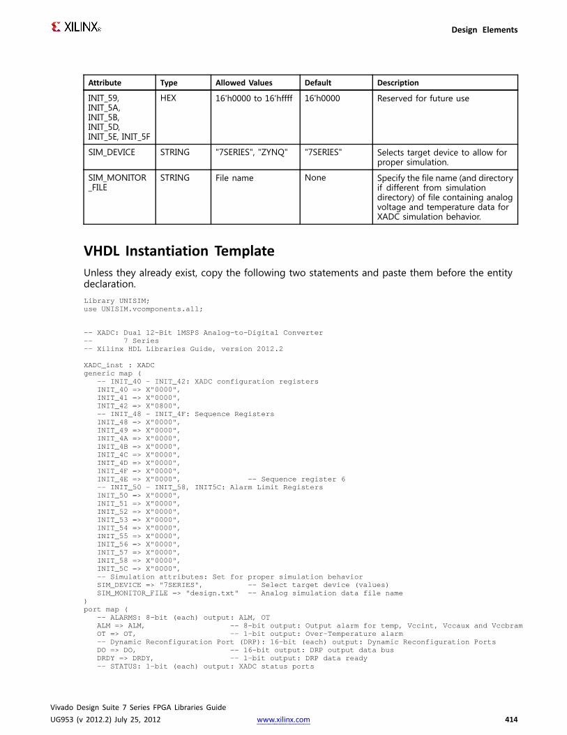
Design Elements
Attribute Type Allowed Values Default Description
INIT_59,INIT_5A,INIT_5B,INIT_5D,INIT_5E, INIT_5F
HEX 16'h0000 to 16'hffff 16'h0000 Reserved for future use
SIM_DEVICE STRING "7SERIES", "ZYNQ" "7SERIES" Selects target device to allow forproper simulation.
SIM_MONITOR_FILE
STRING File name None Specify the file name (and directoryif different from simulationdirectory) of file containing analogvoltage and temperature data forXADC simulation behavior.
VHDL Instantiation TemplateUnless they already exist, copy the following two statements and paste them before the entitydeclaration.Library UNISIM;use UNISIM.vcomponents.all;
-- XADC: Dual 12-Bit 1MSPS Analog-to-Digital Converter-- 7 Series-- Xilinx HDL Libraries Guide, version 2012.2
XADC_inst : XADCgeneric map (
-- INIT_40 - INIT_42: XADC configuration registersINIT_40 => X"0000",INIT_41 => X"0000",INIT_42 => X"0800",-- INIT_48 - INIT_4F: Sequence RegistersINIT_48 => X"0000",INIT_49 => X"0000",INIT_4A => X"0000",INIT_4B => X"0000",INIT_4C => X"0000",INIT_4D => X"0000",INIT_4F => X"0000",INIT_4E => X"0000", -- Sequence register 6-- INIT_50 - INIT_58, INIT5C: Alarm Limit RegistersINIT_50 => X"0000",INIT_51 => X"0000",INIT_52 => X"0000",INIT_53 => X"0000",INIT_54 => X"0000",INIT_55 => X"0000",INIT_56 => X"0000",INIT_57 => X"0000",INIT_58 => X"0000",INIT_5C => X"0000",-- Simulation attributes: Set for proper simulation behaviorSIM_DEVICE => "7SERIES", -- Select target device (values)SIM_MONITOR_FILE => "design.txt" -- Analog simulation data file name
)port map (
-- ALARMS: 8-bit (each) output: ALM, OTALM => ALM, -- 8-bit output: Output alarm for temp, Vccint, Vccaux and VccbramOT => OT, -- 1-bit output: Over-Temperature alarm-- Dynamic Reconfiguration Port (DRP): 16-bit (each) output: Dynamic Reconfiguration PortsDO => DO, -- 16-bit output: DRP output data busDRDY=> DRDY, -- 1-bit output: DRP data ready-- STATUS: 1-bit (each) output: XADC status ports
Vivado Design Suite 7 Series FPGA Libraries GuideUG953 (v 2012.2) July 25, 2012 www.xilinx.com 414

Design Elements
BUSY => BUSY, -- 1-bit output: ADC busy outputCHANNEL=> CHANNEL, -- 5-bit output: Channel selection outputsEOC => EOC, -- 1-bit output: End of ConversionEOS => EOS, -- 1-bit output: End of SequenceJTAGBUSY=> JTAGBUSY, -- 1-bit output: JTAG DRP transaction in progress outputJTAGLOCKED=> JTAGLOCKED, -- 1-bit output: JTAG requested DRP port lockJTAGMODIFIED => JTAGMODIFIED, -- 1-bit output: JTAG Write to the DRP has occurredMUXADDR=> MUXADDR, -- 5-bit output: External MUX channel decode-- Auxiliary Analog-Input Pairs: 16-bit (each) input: VAUXP[15:0], VAUXN[15:0]VAUXN=> VAUXN, -- 16-bit input: N-side auxiliary analog inputVAUXP => VAUXP, -- 16-bit input: P-side auxiliary analog input-- CONTROLand CLOCK: 1-bit (each) input: Reset, conversion start and clock inputsCONVST=> CONVST, -- 1-bit input: Convert start inputCONVSTCLK=> CONVSTCLK, -- 1-bit input: Convert start inputRESET => RESET, -- 1-bit input: Active-high reset-- Dedicated Analog Input Pair: 1-bit (each) input: VP/VNVN => VN, -- 1-bit input: N-side analog inputVP => VP, -- 1-bit input: P-side analog input-- Dynamic Reconfiguration Port (DRP): 7-bit (each) input: Dynamic Reconfiguration PortsDADDR=> DADDR, -- 7-bit input: DRP address busDCLK => DCLK, -- 1-bit input: DRP clockDEN => DEN, -- 1-bit input: DRP enable signalDI => DI, -- 16-bit input: DRP input data busDWE=> DWE -- 1-bit input: DRP write enable
);
-- End of XADC_inst instantiation
Verilog Instantiation Template
// XADC: Dual 12-Bit 1MSPS Analog-to-Digital Converter// 7 Series// Xilinx HDL Libraries Guide, version 2012.2
XADC #(// INIT_40 - INIT_42: XADC configuration registers.INIT_40(16'h0000),.INIT_41(16'h0000),.INIT_42(16'h0800),// INIT_48 - INIT_4F: Sequence Registers.INIT_48(16'h0000),.INIT_49(16'h0000),.INIT_4A(16'h0000),.INIT_4B(16'h0000),.INIT_4C(16'h0000),.INIT_4D(16'h0000),.INIT_4F(16'h0000),.INIT_4E(16'h0000), // Sequence register 6// INIT_50 - INIT_58, INIT5C: Alarm Limit Registers.INIT_50(16'h0000),.INIT_51(16'h0000),.INIT_52(16'h0000),.INIT_53(16'h0000),.INIT_54(16'h0000),.INIT_55(16'h0000),.INIT_56(16'h0000),.INIT_57(16'h0000),.INIT_58(16'h0000),.INIT_5C(16'h0000),// Simulation attributes: Set for proper simulation behavior.SIM_DEVICE("7SERIES"), // Select target device (values).SIM_MONITOR_FILE("design.txt") // Analog simulation data file name
)XADC_inst (
// ALARMS: 8-bit (each) output: ALM, OT.ALM(ALM), // 8-bit output: Output alarm for temp, Vccint, Vccaux and Vccbram.OT(OT), // 1-bit output: Over-Temperature alarm// Dynamic Reconfiguration Port (DRP): 16-bit (each) output: Dynamic Reconfiguration Ports.DO(DO), // 16-bit output: DRP output data bus.DRDY(DRDY), // 1-bit output: DRP data ready
Vivado Design Suite 7 Series FPGA Libraries GuideUG953 (v 2012.2) July 25, 2012 www.xilinx.com 415

Design Elements
// STATUS: 1-bit (each) output: XADC status ports.BUSY(BUSY), // 1-bit output: ADC busy output.CHANNEL(CHANNEL), // 5-bit output: Channel selection outputs.EOC(EOC), // 1-bit output: End of Conversion.EOS(EOS), // 1-bit output: End of Sequence.JTAGBUSY(JTAGBUSY), // 1-bit output: JTAG DRP transaction in progress output.JTAGLOCKED(JTAGLOCKED), // 1-bit output: JTAG requested DRP port lock.JTAGMODIFIED(JTAGMODIFIED), // 1-bit output: JTAG Write to the DRP has occurred.MUXADDR(MUXADDR), // 5-bit output: External MUX channel decode// Auxiliary Analog-Input Pairs: 16-bit (each) input: VAUXP[15:0], VAUXN[15:0].VAUXN(VAUXN), // 16-bit input: N-side auxiliary analog input.VAUXP(VAUXP), // 16-bit input: P-side auxiliary analog input// CONTROLand CLOCK: 1-bit (each) input: Reset, conversion start and clock inputs.CONVST(CONVST), // 1-bit input: Convert start input.CONVSTCLK(CONVSTCLK), // 1-bit input: Convert start input.RESET(RESET), // 1-bit input: Active-high reset// Dedicated Analog Input Pair: 1-bit (each) input: VP/VN.VN(VN), // 1-bit input: N-side analog input.VP(VP), // 1-bit input: P-side analog input// Dynamic Reconfiguration Port (DRP): 7-bit (each) input: Dynamic Reconfiguration Ports.DADDR(DADDR), // 7-bit input: DRP address bus.DCLK(DCLK), // 1-bit input: DRP clock.DEN(DEN), // 1-bit input: DRP enable signal.DI(DI), // 16-bit input: DRP input data bus.DWE(DWE) // 1-bit input: DRP write enable
);
// End of XADC_inst instantiation
For More InformationSee the 7 series FPGA User Documentation (User Guides and Data Sheets).
Vivado Design Suite 7 Series FPGA Libraries GuideUG953 (v 2012.2) July 25, 2012 www.xilinx.com 416


