Summary This application note describes how to interface a Fujitsu MB86064 digital-to-analog converter (DAC) with parallel low-voltage differential signaling (LVDS) inputs to a Virtex®-5 FPGA utilizing the dedicated I/O functions of the FPGA family. The application note and reference design also illustrate a basic LVDS interface for connecting to any DAC converter with high-speed parallel interfaces.
Introduction This application note provides a solution for a Virtex-5 FPGA interface and a high-speed MB86064 or MB86065 DAC from Fujitsu. The implementation is demonstrated in hardware using the DK86065-2 Fujitsu development kit and the Xilinx® ML550 and ML555 demonstration boards. Fujitsu has developed a passive interface adapter module for this purpose.
Three implementations are described in this application note. All make use of the OSERDES I/O features of the Virtex-5 FPGA. The reference applications can be extended in resolution width and speed and can thus be used in a wide range of applications. At the same time, this application note and reference design describe techniques that can be used to interface the Virtex-5 FPGA to other types of DAC components.
The Fujitsu MB86065 is a 14-bit, 1+ Gigasamples per second (GSPS) digital-to-analog converter that is backward compatible with the MB86064. Data input to the DAC is done via high-speed LVDS ports. The port operates in double data rate (DDR) mode with data registered on both rising and falling edges. Alternatively, the device can be configured as a multiplexed dual-port single DAC. To simplify system integration, the DAC is clocked at half the DAC conversion rate. These DACs have a wide application range:
• Code Division Multiple Access (CDMA), Wideband Code Division Multiple Access (W-CDMA), Global System for Mobile Communication (GSM), Enhanced Data rates for GSM Evolution (EDGE), and Universal Mobile Telecommunications System (UMTS)
• Wideband communications systems
• High sample rate direct-IF architectures
• Arbitrary waveform generation
• Test equipment
• Radar, video, and display systems
DAC LVDS Interface
The DAC has two LVDS clock outputs: CLK1_OUT and CLK2_OUT. Two clocks are provided to enable synchronization between different data devices. For the interface of the Virtex-5 FPGA, only one clock is needed. These two clock outputs can be configured (using division factor or delay setting) by a Fujitsu serial control interface.
The DAC has two 14-bit LVDS data input buses. Each input bus has on-chip 100Ω termination resistors to simplify PCB design and reduce the number of external components needed. The DAC LVDS inputs require 14-bit unsigned binary data with bit 14 as the MSB. Data presented to the DAC is shown in Figure 1.
Application Note: Virtex-5 FPGAs
XAPP873 (v1.2) June 15, 2010
Virtex-5 FPGA Interface for Fujitsu Digital-to-Analog Converters with LVDS InputsAuthor: Marc Defossez
To help achieve the timing requirements of the DAC, a set of adjustable loop clock pass-through buffers is implemented in the DAC. These clock feedback buffers have the same characteristics as the data input buffers and are used to aid a digital clock manager (DCM) or phase-locked loop (PLL) in the FPGA, aligning the clock edge and the data for the DAC up to the LVDS input buffers of the DAC. Figure 2 shows a basic data, clock, and clock feedback setup.
A Fujitsu proprietary serial control interface (SCI) can be used to change the different settings for the clock, data, and loopback interface. This SCI is not discussed in this document. An implementation of this protocol is similar to a system packet interface (SPI) implementation and can be done using a PicoBlaze™ processor in the FPGA.
I/O Architecture of Virtex-5 FPGA
I/O Block
The I/O block (IOB) in the Virtex-5 FPGA contains only input and output buffers, as shown in section A of Figure 3. Two IOB blocks can be paired to form a differential I/O, as shown in section B of Figure 3. When the input buffer of a clock-capable I/O is used as a clock input, a direct route passes the clock to the I/O clock buffer (BUFIO) and the regional clock buffer (BUFR). The input buffer is used as a source for ILOGIC/ISERDES or passed directly to the FPGA logic grid. The output buffer can have a connection from OLOGIC/OSERDES or logic grid. An optional inverter can be programmed in the input path of the IOB. The output buffer can be put into a high-Z state, and two coupled output buffers can function as a differential output pair.
X-Ref Target - Figure 1
Figure 1: Odd and Even Data Sampling
X-Ref Target - Figure 2
Figure 2: Basic Data, Clock, and Clock Feedback Setup
Figure 4 shows the setup of a differential I/O pair with IODELAY, ISERDES, and OSERDES. In this application note, the OSERDES block is used to shift data at high speed towards the DAC while the logic of the FPGA runs at a slower speed.
OSERDES loads parallel data at the rising edge of CLKDIV and transmits this data serially to the IOB output buffer at CLK rate. CLK and CLKDIV are related by the input width and use mode of OSERDES. OSERDES can be set up as a:
• Master or master-slave
• 4-, 6-, 8-, or 10-bit input in DDR mode
• 8- and 10-bit inputs are only available in master-slave configuration
• 2-, 3-, 4-, 5-, 6-, 7-, or 8-bit input in single data rate (SDR) mode
• High-Z state-capable output buffer (OBUF)
For the DAC interface, the OSERDES is used in master-slave, 8-bit DDR mode. The CLKDIV rate must be set to be one-fourth of the CLK rate. When using the OSERDES, these points should be taken into consideration:
• The OCE input of OSERDES is not a CE pin for the data inputs of OSERDES. The OCE pin acts at the serial shift output side of OSERDES.
• After releasing the OSERDES reset, nothing happens until the first rising CLKDIV edge. At the moment that data on pins D1 to D6 is loaded into OSERDES, a controller is started to shift data out of OSERDES.
• Because the controller starts when new data is loaded in the parallel registers, it takes a few CLK cycles before data first appears at the output of the OSERDES. For example, in an OSERDES in DDR, 8-bit mode (master-slave configuration), after releasing reset and loading data into OSERDES on the rising CLKDIV edge, it takes four CLK cycles before data appears at the OSERDES output. It takes four CLK cycles because eight bits are loaded into OSERDES and the controller first shifts the eight previous bits, which are all 0, out of OSERDES at CLK DDR rate.
• Upon the first load after reset, data is shifted in regular patterns.
• When started, the OSERDES controller always flushes out the same number of bits that are used by or programmed into OSERDES before loading new data from the input register.
• New data can always be loaded in OSERDES. The controller in OSERDES first completes the shift operation of the data in the serializer and then loads new data into the serializer from the input register. For example, a clock can easily be generated in this manner:
• The OSERDES input is tied to fixed values that match the way the clock cycle looks.
• One rising CLKDIV edge is applied to OSERDES.
• The data is loaded into OSERDES.
• The first time after reset, OSERDES flushes its serial register. From then on, the loaded pattern is shifted out. Because no new data is loaded into OSERDES, the old data is taken again to get shifted out, thus generating a clock pattern.
OSERDES can be used in combination with the IODELAY configured as ODELAY. The delay between the OSERDES output and the FPGA output (die pad or package ball) can be statically configured. Figure 5 shows an OSERDES-IODELAY combination with available FPGA routing. In this figure, PiP stands for Programmable Interconnect Point.
The bold OSERDES settings in Figure 5 are used in this application note. For a complete description of OSERDES, refer to the Virtex-5 FPGA User Guide [Ref 1].
FPGA Interface This section describes the reference design implementation of the DAC interface.
Clock Generation and Feedback
Nearly all DAC devices deliver a clock to the interfacing component. The data produced by the interfacing component (an FPGA) must be presented to the DAC in relationship to this clock. The most commonly used DAC connections in relationship to the DAC input clock are:
• The DAC supplies a clock to the interfacing FPGA and requires data at its input pins 90° phase shifted to or in phase with this clock.
• The DAC supplies a clock and requires a clock and data from the interfacing FPGA. Clock and data must be presented at the device input pins in phase or shifted by 90°.
• The DAC supplies a clock and only requires data. The DAC contains a delay-locked loop (DLL) or PLL and a FIFO to capture and align data.
The MB6806x DAC device delivers a high-speed clock to the FPGA. This requires the data from the FPGA to be delivered to the DAC pins 90° phase shifted to the supplied clock. The
clock is used in the DAC to capture the supplied data. The FPGA device has some features that enable it to achieve the clock-data relation requirement. The PLL or DCM in the FPGA is tuned using a feedback delay loop reaching into the DAC, allowing easier clock-data alignment.
The clock delivered by the DAC is a high-speed clock at half the sample frequency of the DAC. For the reference design and DAC discussed in this application note, the clock has a frequency rate up to 700 MHz. The interface design in the FPGA does not function at this speed but at a divided version of the clock. The high-speed clock is only used to shift the data out to the DAC. Shifting the data out to the DAC means that the OSERDES components in the FPGA are used. The divided clock is a function of the number of bits used for OSERDES.
This setup requires the clock to be fed into the FPGA through a global clock input and handled by a DCM or PLL. A DCM or PLL provide a fully digital, dedicated, on-chip clock deskew. The deskew feature provides zero propagation delay between the source and output clocks, low clock skew among output clock signals distributed throughout the device, and advanced clock domain control. For the DAC application, this deskew is not sufficient because the data must be delivered to the DAC with a known phase relationship to the incoming clock supplied by the DAC. To do this, the feedback path of the DCM or PLL must be taken off-chip, put onto the PCB, and returned to the DCM or PLL feedback pin. The FPGA design now complies with the requirements for the DAC.
Varying only the PCB routing requires the feedback trace to be well matched to the distance between the FPGA and the DAC. Referring to Figure 6, the feedback path on the PCB (“Length B”) must be twice as long as the datapaths between the FPGA and the DAC (“Length A”). It becomes increasingly difficult to maintain valid clock-to-data timing at higher clock rates. Even small mismatches in PCB routing, tolerances over device-to-device variations, and compensation for temperature and stress can require a respin of the PCB or an FPGA-implemented solution.
The MB8606x DAC minimizes these potential problems by an on-chip programmable clock loopback circuit. This circuit comprises a differential input buffer, configurable delay element, and differential output buffer. This DAC feature provides the DCM/PLL and interface circuit a means for adjustment of the clock-data relationship. Matching the feedback PCB traces is still a requirement but the pass-through loopback circuit of the DAC can compensate for device process variations and temperature. The loopback delay in the DAC can be adjusted in real time by use of the serial control interface. Figure 2 shows the basic FPGA setup using the loopback delay in the DAC.
A DCM can be used when the input clock frequency from the DAC is less than or equal to 500 MHz. A PLL can be used when the input clock frequency is greater than 550 MHz and less than 700 MHz. When OSERDES are used in master-slave, 8-bit, DDR mode, the clock for the interface logic must run at one-fourth of the input clock rate. For example:
• DAC performance = 1.2 GSPS.
• Input clock = 600 MHz. In this case, a PLL is needed.
CLK, the clock for the OSERDES serial shift clock input, is routed through a BUFG and the BUFIO in the I/O bank. This clock is only used for the OSERDES CLK inputs. The divided clock is routed through a BUFG and then used as the clock for all of the interface logic, including the parallel load clock of OSERDES.
The feedback clock is generated by an OSERDES, and after routing on the PCB and pass-through DAC circuit, it is taken back into the FPGA via a global clock input buffer, as shown in Figure 7. The software is notified of the external feedback loop by the FEEDBACK constraint. The FEEDBACK constraint syntax is:
NET <feedback_signal> FEEDBACK = <value> ns NET <output_signal>;
Where:
<feedback_signal> is the net that drives the feedback input pin of the DCM/PLL
<output_signal> is the net that drives the output pad
<value> provides the path delay from the output pad to the input padX-Ref Target - Figure 7
Figure 7: Clock Generation Using an OSERDES
X873_07_110509
01010101
A Fixed Input Pattern Like 01010101Or A ROM Can Be Connected Here,Providing the Ability To GenerateDifferent Waveforms
Using OSERDES to generate a clock signal has these advantages:
• The clock cycle can be fixed or programmable.
• When the clock cycle needs to be fixed, the OSERDES data inputs should be tied to High or Low values to match the clock cycle. One rising CLKDIV edge is enough to start the generation of the clock. Refer to “OSERDES and IODELAY,” page 4.
• When the clock cycle needs to be programmable, the OSERDES inputs should be tied to a ROM and the ROM should be cycled through when new clock formats are needed.
• The clock output is normally in phase with the data.
• The timing for all OSERDES in an FPGA is equal. When OSERDES are used to generate data and clock, the outputs of the FPGA swap in phase.
• It is easy to apply a known phase shift to the clock opposed to the data.
• For a fixed clock output, when the 1 and 0 inputs are swapped, the generated clock phase shifts over 180°.
• When OSERDES is clocked using a phase shifted high-speed clock, it is possible to phase shift the clock over 90°. The PLL should generate a 90° phase shifted high-speed clock or the CLK90 output of the DCM should be used. That output should be used to clock the OSERDES CLK pin.
Data for the DAC can be generated in different ways. Three such methods are described here.
Generate Data Using Initialized Block RAM
An initialized block RAM connected to the OSERDES inputs holds the data to be transmitted by OSERDES. The block RAM used as ROM only needs an address counter for reading of the data, as shown in Figure 8, and is clocked by the CLKDIV version of the clock.
A disadvantage of this method is that the data stored in the ROM or RAM must be organized in the same manner as it is to be loaded into OSERDES. If OSERDES is used in 8-bit mode, each OSERDES on the data bus to the DAC must be loaded eight times the same bit number. This is shown in Figure 9.
The ROM-based interface provides a simple solution for this high-speed interface. The reference design provides Excel spreadsheets as aids to block RAM initialization. The spreadsheets help with:
• Generation of ROM content for use in HDL code initialization
• Generation of .mem files for use with the auto-Data2MEM tool function or user-called Data2MEM tool
ISE® software contains a tool known as Data2MEM that changes block RAM initialization in the bitstream. Thus, it is not necessary to run the ISE software flow again when block RAM data has to be changed. In ISE software version 10.1, this Data2MEM functionality can automatically be used by specifying an initialization file for each block RAM component that is used.
Another solution for the high-speed interface is that the initialized data of the block RAM (or ROM) is altered via the second port of the dual-port block RAM by the application.
Design Tip: Not all data bits of the block RAM are used. These bits can be used as address counters. The method of doing this is demonstrated in the WaveGenerator file contained in the reference design ZIP file.
When using block RAM as ROM and connecting to 14 OSERDES in 8-bit mode for a 14-bit resolution DAC, 112 data bits are needed. RAMB36 components of Virtex-5 FPGAs in 32-bit wide data mode provide 32 data bits (DO) and 4 parity bits (DOP) for a memory address depth of 1024. 112 data bits means that four block RAM components are needed. The construction can be set up as:
• Data and parity bits used: For three block RAMs, all data and parity bits are used(3 x 36 = 108 bits). One block RAM only uses the parity bits (4 bits).
• Only data bits used: For three block RAMs, all data bits are used (3 x 32 = 96 bits). One block RAM only uses 16 data bits.
In both setups, the remaining data bits can be used as address counter bits in a self-addressing FIFO scheme as explained in the Self-Addressing FIFO application note [Ref 2]. Using
OSERDES in 4-bit mode only requires two block RAMs but the application/interface clock frequency doubles.
A 1.2 GSPS DAC provides a reference clock. This is the OSERDES CLK clock of 600 MHz. Using OSERDES in 8-bit mode sets CLKDIV to 150 MHz. Using OSERDES in 4-bit mode requires a CLKDIV of 300 MHz.
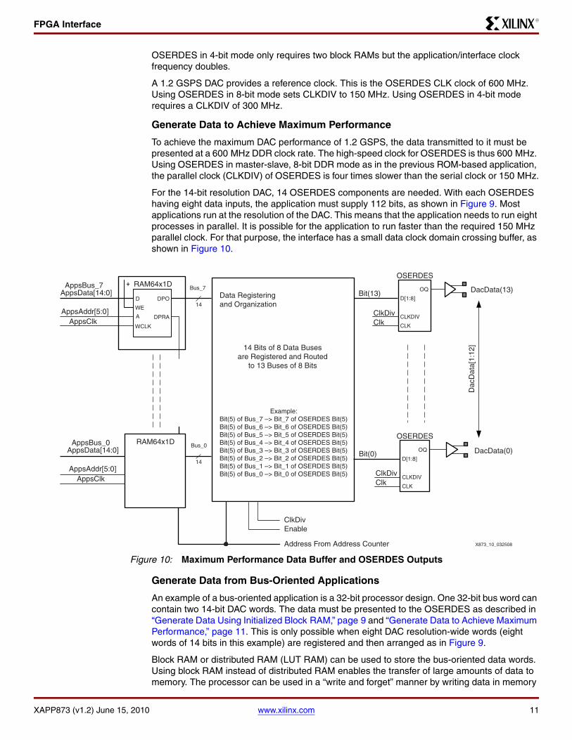
Generate Data to Achieve Maximum Performance
To achieve the maximum DAC performance of 1.2 GSPS, the data transmitted to it must be presented at a 600 MHz DDR clock rate. The high-speed clock for OSERDES is thus 600 MHz. Using OSERDES in master-slave, 8-bit DDR mode as in the previous ROM-based application, the parallel clock (CLKDIV) of OSERDES is four times slower than the serial clock or 150 MHz.
For the 14-bit resolution DAC, 14 OSERDES components are needed. With each OSERDES having eight data inputs, the application must supply 112 bits, as shown in Figure 9. Most applications run at the resolution of the DAC. This means that the application needs to run eight processes in parallel. It is possible for the application to run faster than the required 150 MHz parallel clock. For that purpose, the interface has a small data clock domain crossing buffer, as shown in Figure 10.
Generate Data from Bus-Oriented Applications
An example of a bus-oriented application is a 32-bit processor design. One 32-bit bus word can contain two 14-bit DAC words. The data must be presented to the OSERDES as described in “Generate Data Using Initialized Block RAM,” page 9 and “Generate Data to Achieve Maximum Performance,” page 11. This is only possible when eight DAC resolution-wide words (eight words of 14 bits in this example) are registered and then arranged as in Figure 9.
Block RAM or distributed RAM (LUT RAM) can be used to store the bus-oriented data words. Using block RAM instead of distributed RAM enables the transfer of large amounts of data to memory. The processor can be used in a “write and forget” manner by writing data in memory
X-Ref Target - Figure 10
Figure 10: Maximum Performance Data Buffer and OSERDES Outputs
X873_10_032508
+AppsBus_7AppsData[14:0]
AppsAddr[5:0]AppsClk
AppsBus_0AppsData[14:0]
AppsAddr[5:0]AppsClk
RAM64x1D
RAM64x1D
OSERDES
OSERDES
Bit(13)
Bit(0)
Dac
Dat
a[1:
12]
DacData(0)
DacData(13)Bus_7
Bus_0
14
14
ClkDivEnable
Address From Address Counter
ClkDivClk
ClkDivClk
OQ
OQ
D[1:8]
CLKDIV
CLK
D[1:8]
CLKDIV
CLK
D
WE
A
WCLK
DPO
DPRA
Data Registeringand Organization
14 Bits of 8 Data Busesare Registered and Routed
to 13 Buses of 8 Bits
Example:Bit(5) of Bus_7 –> Bit_7 of OSERDES Bit(5)Bit(5) of Bus_6 –> Bit_6 of OSERDES Bit(5)Bit(5) of Bus_5 –> Bit_5 of OSERDES Bit(5)Bit(5) of Bus_4 –> Bit_4 of OSERDES Bit(5)Bit(5) of Bus_3 –> Bit_3 of OSERDES Bit(5)Bit(5) of Bus_2 –> Bit_2 of OSERDES Bit(5)Bit(5) of Bus_1 –> Bit_1 of OSERDES Bit(5)Bit(5) of Bus_0 –> Bit_0 of OSERDES Bit(5)
and continuing with something else until new data is available or until the interface asks for new data. Data from the application is written in a ping-pong type addressed set of block RAMs. This setup doubles the depth of the block RAM, as shown in Figure 11. One of the DAC words (bits [29:16]) enters channel 1 while the other DAC word (bits [13:0]) enters channel 0. The blocks used for both channels are identical.
Ping-pong addressing means that data on even addresses is written (port_A) in one memory while data on odd addresses is stored in a second memory. Address bit 0 is the selection bit to enable the block RAM and the other address bits to form the write address. At the read side (port_B), data from both memories is handled as independent data and can be read at half the write clock rate. The write side of the block RAM is clocked at the speed of the processor application, assuming 200 MHz as an example.
Two write operations result in a double 32-bit (4 x 14 bits) word ready for a read operation. The read side of the block RAM is clocked at half the rate of the write side (100 MHz) because two 32-bit words are read at once. Two read operations are required to assemble the eight 14-bit words (112 bits) that need to be loaded into OSERDES. The load of the OSERDES components thus happens at half the rate of the block RAM read or 50 MHz, as shown in Figure 10. OSERDES is used in DDR mode, thus the serial shift clock for the OSERDES components must be four times that of the parallel clock. The serial shift clock is then 200 MHz, and the data rate at the OSERDES output is 400 Mb/s.
Different circuit components should be placed as close as possible to each other on the PCB, aligned according to the pinout of the components. Components should be positioned to minimize the number of turns, corners, and vias. The flexibility of the FPGA pinout can assist in optimizing the PCB routing. A straight, short connection improves all possible parameters of a PCB layout, namely:
• Signal integrity
• Transmission line effects
• Capacitance and inductance
• Operating frequency
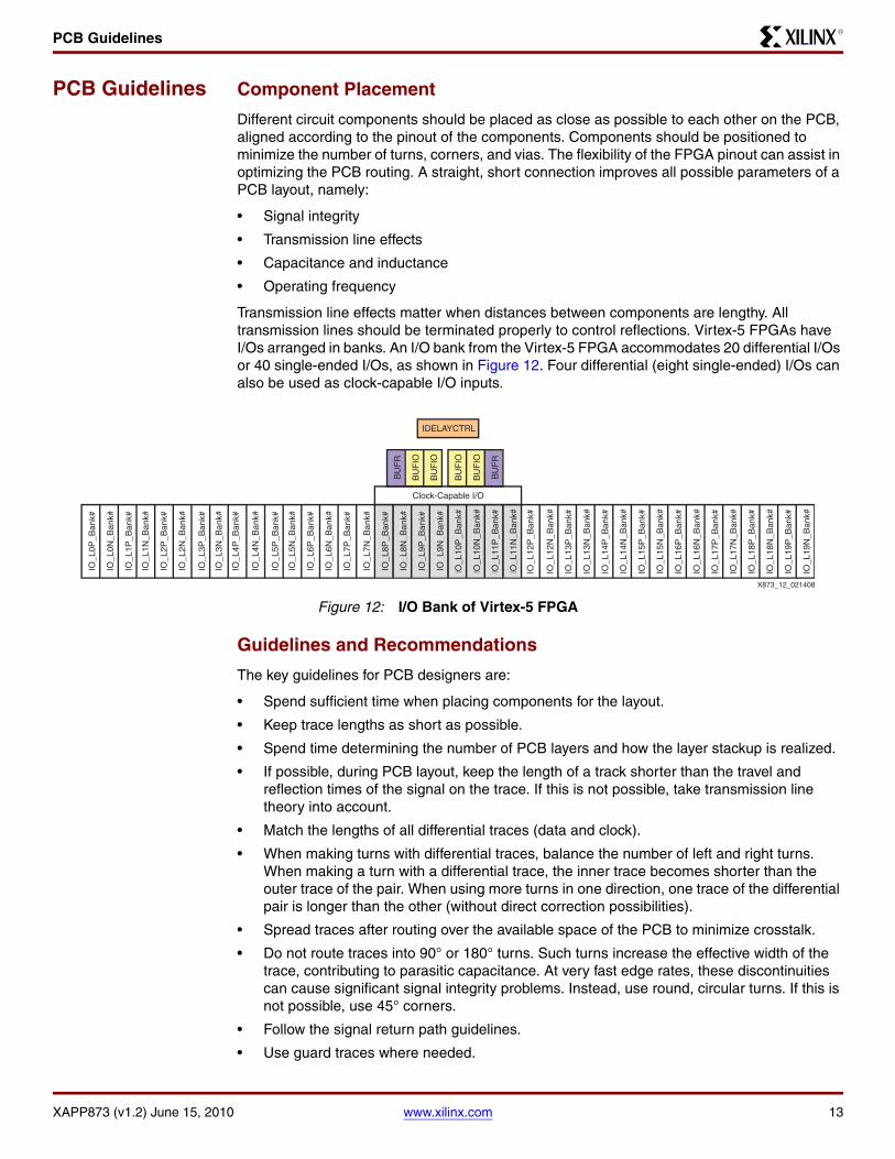
Transmission line effects matter when distances between components are lengthy. All transmission lines should be terminated properly to control reflections. Virtex-5 FPGAs have I/Os arranged in banks. An I/O bank from the Virtex-5 FPGA accommodates 20 differential I/Os or 40 single-ended I/Os, as shown in Figure 12. Four differential (eight single-ended) I/Os can also be used as clock-capable I/O inputs.
Guidelines and Recommendations
The key guidelines for PCB designers are:
• Spend sufficient time when placing components for the layout.
• Keep trace lengths as short as possible.
• Spend time determining the number of PCB layers and how the layer stackup is realized.
• If possible, during PCB layout, keep the length of a track shorter than the travel and reflection times of the signal on the trace. If this is not possible, take transmission line theory into account.
• Match the lengths of all differential traces (data and clock).
• When making turns with differential traces, balance the number of left and right turns. When making a turn with a differential trace, the inner trace becomes shorter than the outer trace of the pair. When using more turns in one direction, one trace of the differential pair is longer than the other (without direct correction possibilities).
• Spread traces after routing over the available space of the PCB to minimize crosstalk.
• Do not route traces into 90° or 180° turns. Such turns increase the effective width of the trace, contributing to parasitic capacitance. At very fast edge rates, these discontinuities can cause significant signal integrity problems. Instead, use round, circular turns. If this is not possible, use 45° corners.
• When available, use the thermal pad connection at the bottom side of DAC device packages to improve the operating stability of the device.
Reference Design
Reference Design Matrix
Running the Reference Design
Instructions on how to operate the reference design on an ML5xx demonstration board are given in the readme file provided with the reference design. The Click here and type Application Note Tile design files can be downloaded from: https://secure.xilinx.com/webreg/clickthrough.do?cid=109750
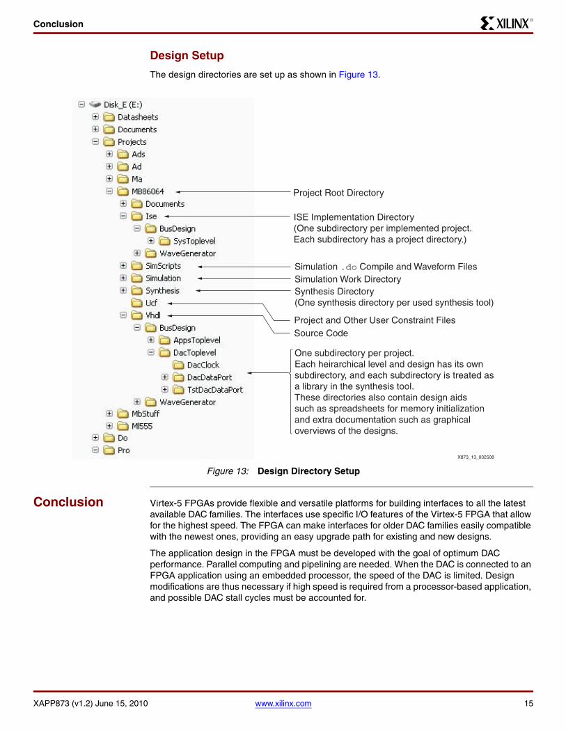
The design directories are set up as shown in Figure 13.
Conclusion Virtex-5 FPGAs provide flexible and versatile platforms for building interfaces to all the latest available DAC families. The interfaces use specific I/O features of the Virtex-5 FPGA that allow for the highest speed. The FPGA can make interfaces for older DAC families easily compatible with the newest ones, providing an easy upgrade path for existing and new designs.
The application design in the FPGA must be developed with the goal of optimum DAC performance. Parallel computing and pipelining are needed. When the DAC is connected to an FPGA application using an embedded processor, the speed of the DAC is limited. Design modifications are thus necessary if high speed is required from a processor-based application, and possible DAC stall cycles must be accounted for.
X-Ref Target - Figure 13
Figure 13: Design Directory Setup
X873_13_032508
Simulation .do Compile and Waveform Files
Synthesis Directory(One synthesis directory per used synthesis tool)
Source CodeProject and Other User Constraint Files
One subdirectory per project.Each heirarchical level and design has its ownsubdirectory, and each subdirectory is treated asa library in the synthesis tool.These directories also contain design aidssuch as spreadsheets for memory initializationand extra documentation such as graphical overviews of the designs.
Project Root Directory
ISE Implementation Directory(One subdirectory per implemented project.Each subdirectory has a project directory.)
3. DS202, Virtex-5 FPGA Data Sheet: DC and Switching Characteristics.
4. UG195, Virtex-5 FPGA Packaging and Pinout Specification.
5. UG203, Virtex-5 FPGA PCB Designer’s Guide.
Revision History
The following table shows the revision history for this document:
Notice of Disclaimer
Xilinx is disclosing this Application Note to you “AS-IS” with no warranty of any kind. This Application Noteis one possible implementation of this feature, application, or standard, and is subject to change withoutfurther notice from Xilinx. You are responsible for obtaining any rights you may require in connection withyour use or implementation of this Application Note. XILINX MAKES NO REPRESENTATIONS ORWARRANTIES, WHETHER EXPRESS OR IMPLIED, STATUTORY OR OTHERWISE, INCLUDING,WITHOUT LIMITATION, IMPLIED WARRANTIES OF MERCHANTABILITY, NONINFRINGEMENT, ORFITNESS FOR A PARTICULAR PURPOSE. IN NO EVENT WILL XILINX BE LIABLE FOR ANY LOSS OFDATA, LOST PROFITS, OR FOR ANY SPECIAL, INCIDENTAL, CONSEQUENTIAL, OR INDIRECTDAMAGES ARISING FROM YOUR USE OF THIS APPLICATION NOTE.
Date Version Description of Revisions
05/06/08 1.0 Initial Xilinx release.
12/07/09 1.1 Confirmed in “OSERDES and IODELAY,” page 4 that the delay between the OSERDES output and FPGA output can only be statically configured. Added explanation of PiP before Figure 5, page 5. Removed BUFIO from Figure 7, page 7.
06/15/10 1.2 In Figure 6 and the paragraph above Figure 6, corrected the relative length of data to clock feedback PCB paths (Length A and Length B).