Xilinx/Cadence PCB Guide UG629 (v 13.2) July 6, 2011 This document applies to the following software versions: ISE Design Suite 13.2 and later This document applies to the following software versions: ISE Design Suite 13.2 and later This document applies to the following software versions: ISE Design Suite 13.2 and later This document applies to the following software versions: ISE Design Suite 13.2 and later
Transcript
Xilinx/Cadence PCB Guide
UG629 (v 13.2) July 6, 2011
This document applies to the following software versions: ISE Design Suite 13.2 and laterThis document applies to the following software versions: ISE Design Suite 13.2 and laterThis document applies to the following software versions: ISE Design Suite 13.2 and laterThis document applies to the following software versions: ISE Design Suite 13.2 and later
Xilinx is disclosing this user guide, manual, release note, and/or specification (the “Documentation”) to yousolely for use in the development of designs to operate with Xilinx hardware devices. You may not reproduce,distribute, republish, download, display, post, or transmit the Documentation in any form or by any meansincluding, but not limited to, electronic, mechanical, photocopying, recording, or otherwise, without the priorwritten consent of Xilinx. Xilinx expressly disclaims any liability arising out of your use of the Documentation.Xilinx reserves the right, at its sole discretion, to change the Documentation without notice at any time. Xilinxassumes no obligation to correct any errors contained in the Documentation, or to advise you of any correctionsor updates. Xilinx expressly disclaims any liability in connection with technical support or assistance that may beprovided to you in connection with the Information.
THE DOCUMENTATION IS DISCLOSED TO YOU “AS-IS” WITH NOWARRANTY OF ANY KIND. XILINXMAKES NO OTHER WARRANTIES, WHETHER EXPRESS, IMPLIED, OR STATUTORY, REGARDINGTHE DOCUMENTATION, INCLUDING ANY WARRANTIES OF MERCHANTABILITY, FITNESS FOR APARTICULAR PURPOSE, OR NONINFRINGEMENT OF THIRD-PARTY RIGHTS. IN NO EVENT WILLXILINX BE LIABLE FOR ANY CONSEQUENTIAL, INDIRECT, EXEMPLARY, SPECIAL, OR INCIDENTALDAMAGES, INCLUDING ANY LOSS OF DATA OR LOST PROFITS, ARISING FROM YOUR USE OF THEDOCUMENTATION.
Chapter 3 Common Tasks .........................................................................................11
Create an Initial FPGA Pinout............................................................................. 11Create an Initial FPGA I/O User Constraint File (UCF)..................................... 14Create a Schematic Symbol (Schematic Shape and Content) ............................ 15Create a Layout Symbol....................................................................................... 17Map Schematic Symbols to the Layout Symbol................................................. 17Update ISE Software Files with Pinout Changes Made in the Schematic
Tool ............................................................................................................... 18Update the PCBDatabase with Pinout ChangesMade in ISE Software ........... 18Update ISE with Pinout Changes Made in the Layout Tool.............................. 19
Xilinx/Cadence PCB GuideUG629 (v 13.2) July 6, 2011 www.xilinx.com 3
Xilinx/Cadence PCB Guide4 www.xilinx.com UG629 (v 13.2) July 6, 2011
Chapter 1
IntroductionThis guide contains information for FPGA designers and Printed Circuit Board (PCB)engineers about processes and mechanisms available within the Xilinx® ISE® DesignSuite and various Cadence tools to efficiently implement an FPGA on a PCB.
The first section of the guide covers the PCB and FPGA designs flows, highlightingsteps where data is exchanged between these two software environments. Then foreach identified step the guide details processes, files, and options available to performthe identified task.
With Cadence’s broad software package availability, this document cannot coverall of the features available for implementing a printed circuit board with FPGAs.For details about these tools, refer to the Cadence documentation available at:http://www.cadence.com/support/pages/sourcelink.aspx.
If you use software tools from multiple vendors for your PCB design flow, such asCadence OrCAD for schematic capture with Mentor Graphics PADs for PCB layout,refer to vendor specific documentation. For Mentor Graphics tools, refer to theXilinx/Mentor Graphics PCB guide.
Xilinx/Cadence PCB GuideUG629 (v 13.2) July 6, 2011 www.xilinx.com 5
Xilinx/Cadence PCB Guide6 www.xilinx.com UG629 (v 13.2) July 6, 2011
Chapter 2
Implementing a Xilinx FPGA on aPrinted Circuit Board
In recent years, the design of FPGAs and printed circuit boards (PCBs) have becomeincreasingly parallelized as opposed to the traditional sequential model. This is mostlydue to market pressure which demands a fast design cycle and rapid adaptability tospecification changes. In the past the FPGA was typically designed before the board orwas added to an already designed board to perform some glue logic function, voltageor protocol conversion. Often the same PCB engineers were doing both the FPGA andPCB designs.
Today, with their increasing internal and I/O capabilities, FPGAs can take on morecore features of an application which require longer development time and greaterexpertise and manpower. On the board side, tight form factor, signal integrity, andelectromagnetic regulations require sharp skills and dedicated personnel. Therefore,FPGA and PCB are now two separate design teams working in different environmentsand often physically distant.
Paradoxically, pressures in terms of time and adaptability to market requires many moreinteractions between these design environments so that functionality, performance andcost objective are delivered on time. In practice, this translates into back and forth dataexchanges throughout the design process between design teams to update the boardsymbols and FPGA constraints.
Xilinx/Cadence PCB GuideUG629 (v 13.2) July 6, 2011 www.xilinx.com 7
Chapter 2: Implementing a Xilinx FPGA on a Printed Circuit Board
Design FlowThe following System Development Cycle illustration shows a typical flow in the PCBand FPGA development cycle (white boxes). It also highlights the steps that requirecommunication between FPGA and PCB software tools (grey boxes). Common Tasksdetails the mechanisms and processes available to perform each of these data exchanges.
System Design Cycle with FPGA and PCB DatabasesSynchronization Steps Highlighted
PCB design requires two main tools; a schematic capture tool and a layout tool. Thesetools are described in the following sections.
Xilinx/Cadence PCB Guide8 www.xilinx.com UG629 (v 13.2) July 6, 2011
Chapter 2: Implementing a Xilinx FPGA on a Printed Circuit Board
Schematic Capture Tool in the FPGA Design FlowThe schematic capture tool enables designers to create a graphical representation ofconnections between components on the PCB. This data helps anyone involved in theproject to understand how components on this board are connected between themselvesand with the outside world. The layout designer also uses this information to physicallyplace and route all signals on the PCB.
Tips: Since an FPGA is a programmable component, its requirements on the PCB areunique to your application. Xilinx recommends that you add within all the schematicthe specific components necessary for both the programming and the behavior of thisdevice in your particular application.
• Add decoupling capacitors. Since FPGAs can be programmed to perform in a widerange of applications which translate into a wide range of decoupling needs, it is notpractical for Xilinx to embed decoupling networks inside the device. The schematicengineer often adds all the decoupling network details on the schematic so as to letthe PCB designer place these components in the vicinity of the FPGA package.
• Add other external components necessary to enable specific FPGA features. Forinstance the schematic designer needs to attach digitally controlled impedance(DCI) calibration resistors to VRN and VRP pins when I/Os on the device havethe on-chip termination option enabled.
• Add debug, probe, and test points.
• Add pin swapping information. It is often useful at this point to define whichpins can be swapped without violating FPGA pinout rules. This is very usefulinformation for the PCB designer as it provides flexibility when trying to minimizewire crossover, congestion, and signal integrity in placing and routing signals.
PCB Layout Tool in the FPGA Design FlowThe PCB layout tool reads the component and connectivity description in the schematiccapture tool and physically places and routes these components on the PCB. The outputis a set of masks and geometries that allow manufacture of the PCB.
Tips In order to efficiently place and route a programmable device, the PCB designerneeds the following information
• Board physical dimensions. Dimension of the board, mandatory position ofconnectors, etc.
• Stackup dimensions. Number and orientation of signal layers, number and locationof power and ground planes, board material, traces properties, etc.
• Components footprint. Exact dimensions of each component package.
• Components landing pattern. Shape of the junction area between the componentand the board including manufacturing tolerances.
• Board environment properties. Available space around the PCB (air flow, obstacle,vibrations, cooling system, access to power and connectors, etc.)
Cadence PCB Design ToolsBelow is a brief description of the Cadence tool chains and capabilities available fordesigning printed circuit boards. Please refer to the tool's documentation for furtherdetails.
Xilinx/Cadence PCB GuideUG629 (v 13.2) July 6, 2011 www.xilinx.com 9
Chapter 2: Implementing a Xilinx FPGA on a Printed Circuit Board
Cadence OrCAD SeriesThis tool set is typically appropriate for low to medium complexity boards and singlesite design teams. This document refers to Capture as the schematic capture tool andLayout as the layout tool. Depending on your exact software configuration, yourCadence documentation might refer to slightly different names, however all featuresand methodologies presented here are available to you.
Cadence Allegro SeriesThis tool set is typically appropriate for medium to high complexity designs and forsingle to many site design teams. This document refers to Design Entry as the schematiccapture tool and PCB Editor as the layout tool. Depending on your exact softwareconfiguration, your Cadence documentation might refer to slightly different names,however all features and methodologies presented here are available to you.
Multi-Vendor FlowYou can also use multiple vendor software tools for your PCB design. For instance,Cadence OrCAD Capture can be used for schematic capture with Mentor GraphicsPADs or Expedition series for PCB layout. Mentor Graphics users should refer to theXilinx/Mentor Graphics PCB Design Guide for information about Mentor Graphics tools.When using other PCB software packages please refer to your vendor's documentation.
Xilinx/Cadence PCB Guide10 www.xilinx.com UG629 (v 13.2) July 6, 2011
Chapter 3
Common TasksThe following section covers the process, available software features, and filemanipulations needed to accomplish each task in the PCB or FPGA design flow relatedto the FPGA pinout. Each of these tasks is illustrated in the flow chart in chapter 1. Tasksassociated exclusively with either PCB or FPGA design flow are represented as whiteboxes. Tasks common to both design flows are represented as grey shaded boxes.
Create an Initial FPGA PinoutAfter taking into account the system specification describing the different parts andconnectors on the board along with communication channels linking them together, thenext step for the designer is to infer a device and package that can accommodate thesecommunication channels then expand, classify, and assign each signal to a particularpin on the chosen FPGA package. This task requires FPGA architecture knowledgeallowing PCB designers to find an optimal pinout for the PCB design. Therefore, thistask is typically done by an FPGA engineer.
Necessary InformationI/O placement requirements may come from a variety of sources. To save time Xilinxrecommends that you draw the list of I/Os and learn about the FPGA architecture beforestarting I/O placement.
Tip FPGA requirements can be found in the device data sheets and user guides.
• System requirements:
– Identify properties and number of each I/O standards required (includingdirection, input and output voltages, drive strength, slew rate, data rate, etc.).
– Identify differential pairs.
– Identify global/regional clock signal with their associated data signals.
– Identify Multi Gigabit Serial Transceivers.
– List I/O location constraints imposed by predefined IP Blocks (third party IPor IP generated by the CORE Generator™ tool, the Architecture Wizard, theMemory Interface Generator or the Embedded Development Kit (EDK)).
Xilinx/Cadence PCB GuideUG629 (v 13.2) July 6, 2011 www.xilinx.com 11
Chapter 3: Common Tasks
• FPGA Requirements (refer to the device user guides for more information):
– Acquire device knowledge including:
♦ I/O compatibility or I/O banking requirements.
♦ Device package properties such as I/O count for the entire device and perbank and clock region, I/O data rate and signaling capabilities such as singleended/differential or single/dual data rate support, etc.
♦ I/O access to internal resources. Resources such as clock buffer, RAM,serializer/deserializer, etc.
♦ Device clocking capabilities such as internal clock management resources,I/O with direct access to clock networks, etc.
– Reserve and Prohibit usage of special purpose pins:
♦ Prohibit package pins. Because of die or package migration, or futuredesign growth constraints.
♦ Reserve configuration pins.
♦ Reserve JTAG pins.
♦ Reserve DCI pins.
• PCB Requirements:
– Formulate package escape strategies. Determine board number and direction oflayers, pin spacing, etc.
– Signal integrity. Estimate amplitude and timing margins for each signal type.
– Air flow. Ensure work area has sufficient airflow.
– Placement and orientation of neighboring parts which could constrain the FPGAplacement or access of PCB signals to the FPGA.
– Connectivity to other devices. Other device may impact the optimal FPGAI/O design.
ProcessDepending on your preferences and company policies, there are different mechanismsyou can use to assign pins on an FPGA. The following methods are the most common.
Create a Pinout in a Spreadsheet EnvironmentTo create a pinout in a spreadsheet environment, create two spreadsheets, the first withyour design I/O requirements (signal name, I/O standards, direction, etc.), and a secondwith properties for each pin in the package (pin number, I/O bank number, pin name,etc.). Then going down the list of your design signals, filter out and sort package pins ofthe second spreadsheet to determine compatible device I/Os. Finally, go back to youroriginal design I/O spreadsheet and assign pin numbers (or I/O bank numbers) to yoursignal names. Once this is done, you will export this pinout to the schematic and FPGAtools as detailed in the next paragraphs.
This method is most often used by advanced users with extensive knowledge of theFPGA's capabilities. Since there is no DRC done by any tool during this process, theresulting I/O assignment could fail during FPGA or board implementation.
Xilinx/Cadence PCB Guide12 www.xilinx.com UG629 (v 13.2) July 6, 2011
Chapter 3: Common Tasks
Tip You can easily create the package property spreadsheet with one of the following:• Partgen utility. (For example, partgen -v xc5vlx30ff676)• Download the package file for your target:
– Virtex® families: Refer to Answer Record 20578 at:http://www.xilinx.com/support/answers/20578.htm
– Spartan® families: Refer to Answer Record 21035 at:http://www.xilinx.com/support/answers/21035.htm
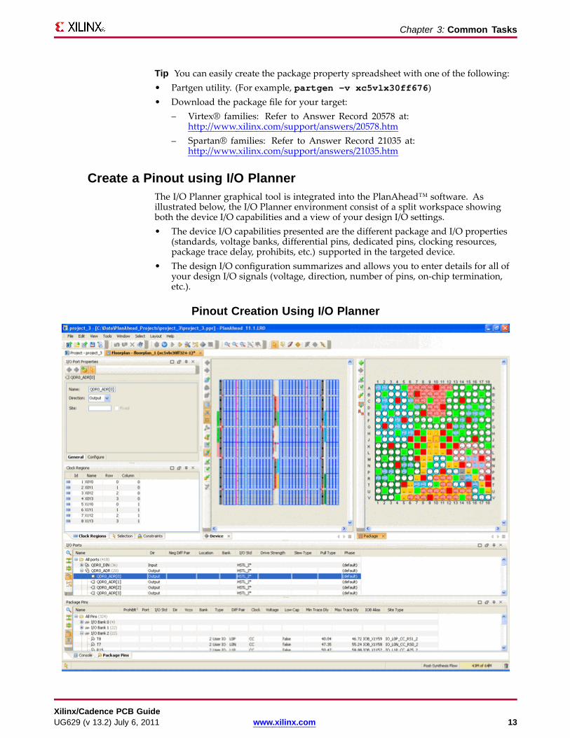
Create a Pinout using I/O PlannerThe I/O Planner graphical tool is integrated into the PlanAhead™ software. Asillustrated below, the I/O Planner environment consist of a split workspace showingboth the device I/O capabilities and a view of your design I/O settings.• The device I/O capabilities presented are the different package and I/O properties
(standards, voltage banks, differential pins, dedicated pins, clocking resources,package trace delay, prohibits, etc.) supported in the targeted device.
• The design I/O configuration summarizes and allows you to enter details for all ofyour design I/O signals (voltage, direction, number of pins, on-chip termination,etc.).
Pinout Creation Using I/O Planner
Xilinx/Cadence PCB GuideUG629 (v 13.2) July 6, 2011 www.xilinx.com 13
You may also import an I/O port list from HDL, CSV or UCF format into I/O Planner.
These views make it simple to identify package pins that support your signal properties.In addition to the interactive mode where you can drag and drop sets of signals intogroups of package pins, you can also enable I/O Planner's I/O placer engine to automateI/O placement.
To check I/O placement against the FPGA pin assignment rules, I/O Planner can preventincorrect assignment on-the-fly or you can run a set of design rules checks. You can alsorun a Weighted Average Simultaneous Switching Output analysis to verify the pinoutis correct.
Finally you can export this pinout to a UCF, CSV, Verilog or VHDL file and read thisinformation into your schematic or spreadsheet entry tool.
For more information on the I/O Planner tool, see the I/O planning section of thePlanAhead User Guide.
Create an Initial FPGA I/O User Constraint File (UCF)In the ISE® Design Suite, I/O constraints can be entered in a unique User ConstraintsFile (UCF) attached to the design project. They can also be attached to the HDL (Verilogor VHDL) source code, the synthesis constraint file (XCF) or embedded in the logicnetlist (NGC, EDF or EDN files, and associated NCF files). The problem with enteringI/O properties and location constraints in multiple files is that maintenance, portabilityand updates to the design become much more complex. Xilinx recommends that youspecify the maximum number of I/O related constraint within a single UCF file.
Create a UCF File with a Text EditorYou can create a UCF file by simply typing the constraints into a text editor. Whencreating a UCF file in this way, please refer to the Constraints Guide for the syntax of all I/Orelated constraints. This method is most often used by companies that have developedtheir own scripts that read in a spreadsheet and convert the data into UCF syntax.
If you already have your I/O constraints defined in a spreadsheet format, you can usethe import function in I/O Planner. In this case, the tool parses your spreadsheet andconverts recognized data into UCF syntax. At a minimum, the Signal Name field mustbe present.
Data is recognized for all column headers that match the following:• Signal Name (Mandatory)• IO Bank• Pin Number• IOB Alias• Site Type• Min/Max Trace Delay• Prohibit• Interface• Direction• DiffPair Type• DiffPair Signal• IO Standard• Drive• Slew Rate
Xilinx/Cadence PCB Guide14 www.xilinx.com UG629 (v 13.2) July 6, 2011
Chapter 3: Common Tasks
For more information on the I/O Planner tool, see the I/O planning section of thePlanAhead User Guide.
Create a UCF with I/O PlannerOnce the pinout is defined, use the "Export I/O ports" command in I/O Planner togenerate the I/O assignment in UCF format.
Create a UCF with the PIN2UCF UtilityWith the other methods for creating a pinout described in this section you can eithercreate a complete pin assignment or create a partial one (assign a signal names to sets ofpin numbers) and let the back-end place and route tool perform the actual assignmentwithin this specified set. In the second case, you can assign a signal or a set of signals toa pin, a set of pins, a bank or a set of banks and thus give the implementation tool thetask of assigning an exact package pin number to each individual user I/O.
If after the implementation you are satisfied with this pinout and want to preserve it forfuture implementation runs then you can do one of the following:
• In Project Navigator go to the Process window and expand the Implement Designprocess. Next, expand the Place & Route process, and double-click Back-AnnotatePin Locations. A UCF file is created and has all your I/O signals locked to a specificpackage pin number.
• Use the PIN2UCF utility to lock a particular pinout for the next implementationiteration. To use the PIN2UCF utility, type the following at the command lint.
Create a Schematic Symbol (Schematic Shape and Content)An FPGA schematic symbol is used to describe the electrical connectivity betweeneach device and its environment (other parts, connectors, etc.). Unlike most othercomponents, FPGA symbols are not likely to be available in a predefined library. Onepurpose of a library is to allow reuse of its elements across different applications.FPGAs, by definition are programmable and application specific so no two designs willhave the same connectivity (signal names and pinout) with the outside world. Thereforefew symbol properties can be reused from one project to another.
Necessary InformationDepending on your Cadence tool flow, an FPGA may be represented either as agraphical symbol to be placed on a schematic or as a spreadsheet. In either case, globalproperties area attached to the resulting representation. As a result, each spreadsheet orsymbol lists available I/Os and may also tag I/Os with its additional properties.
Xilinx/Cadence PCB GuideUG629 (v 13.2) July 6, 2011 www.xilinx.com 15
Chapter 3: Common Tasks
Typically FPGAs have more I/Os than can be represented on a single schematic sheet,therefore FPGA symbols are often split into multiple fractures and hierarchy levels tosimplify readability.Each company and sometimes each engineer has their own processand opinion as to what an FPGA schematic symbol should look like or contain. Below isthe minimum set of data required for an FPGA schematic signal plus some additionalinformation which could make the FPGA schematic symbols more useful.• Graphical symbol - Such that the component can be placed on the schematic.
Choose a shape that allows placement of a fair number of I/Os. Some engineers usea different shape depending on the type of interface.
• Device name - Component ASCII name that makes it easy for someone reading theschematic to know what this component is.
• Reference designator - Unique and short identifier for each component on theschematic.
• I/O name (or pin name) - A separate name for each I/O on the symbol. Xilinxrecommends using the same name as in the top level HDL description. Sincethis is the name FPGA designers will be familiar with, this makes for easiercommunications between Schematic and FPGA designers. In addition each I/Ocan be tagged with additional visible or non-visible properties. Therefore werecommend adding data sheet, pin name, and I/O direction.
• Non-user I/Os - Ensure that all pins available on the package have an entry in theschematic symbol. Some of them may be visible such as unused or logistical I/O(DCI reference). Others may be hidden as they are not of interest for describing theboard functionality, such as power, ground, no connect, or reserved I/Os. Havingall I/Os present on the schematic symbol will be appreciated because it helps withmapping the schematic symbol to the layout symbol. It will also facilitate themaintenance of symbols when pin swaps occur.
• Pin Number - Locates the I/O on the package ball array.
ProcessDepending on the engineers’ preferences and company policies, there are severalmechanisms for creating schematic symbols for FPGAs. Most engineers use one of thethree methods described below.
The basic symbol information such as pin name and pin number may be gathered frommultiple sources. For instance, it can be copied and pasted from the device user guide.This is not recommended since it is easy to mistakenly copy the wrong information oromit some pins. A more common way if you have a placed and routed FPGA design, isto generate the I/O file, called a PAD file, from within the ISE® Design Suite. This PADfile contains all the specific I/O information about your particular design. A PAD filerequires an implemented FPGA design which you may not already have, especially ifthe PCB and FPGA design processes are highly parallel. In such cases you can use theCSV output from an I/O assignment done in I/O Planner. If this information is notavailable, you can create a generic symbol using the Partgen utility. Partgen createsa PKG file containing all I/O names and numbers available on the device. This isessentially the information you can find the within the device user guide with the benefitof being rapidly converted into a spreadsheet.
Tips:• To create a PAD file with ReportGen, type the following:
reportgen ncd_filename –pad
• To get details on all package pins, use the partgen utility:partgen -v target_device
For example:partgen -v xc5vlx30ff676
Xilinx/Cadence PCB Guide16 www.xilinx.com UG629 (v 13.2) July 6, 2011
Chapter 3: Common Tasks
Note When importing PAD files into Cadence tools, you might find some parsing errorsdepending on which version of ISE is combined with which version of Allegro. In suchcases please refer to the Cadence support site (http://www.cadence.com/products/pcb)for a PERL script utility that converts the ISE software file into a format directly readableinto Allegro Librarian.
Create a Schematic Symbol in a Text EditorTo create a schematic symbol in a text editor please refer to OrCAD or Allegro DesignEntry documentation on how to set the location, shape and all other properties of thesymbol.
This method is most often used by companies that have developed their own scriptsthat read in a spreadsheet, HDL, or the post implementation I/O report (PAD file) andautomatically convert the data onto a symbol.
Create a Schematic Symbol with OrCAD CaptureWithin Capture, select the Generate Part option and follow the guided process whichwill successively let you import a spreadsheet based I/O assignment then let you addsymbol graphics and pin properties.
Create a Schematic Symbol with Allegro Design EntryWithin PCB Librarian, directly read in the ISE software PAD file or a I/O Planner CSVspreadsheet and follow the guide process to add pin properties. For instance, Powerpins and unconnected pins can be tagged for special handling.
Tip You can find documentation for displaying "intelligent" symbol graphics to indicatepin type and other useful symbol properties on the IEEE website at http://www.ieee.org.
Create a Layout SymbolThe layout symbol contains the device physical dimensions such that copper traces canbe accurately routed to and from the FPGA pins or balls. The layout symbols are notdesign specific and can therefore be stored in a predefined library and shared amongmany FPGA designs with the same package.
Allegro has dialog boxes that let you enter package physical dimensions such as balllocation and dimension.
Tips• Use the Mechanical Drawing section in the Packaging and Pinout Specification of
the specific device user guide to capture this information.
• Go to www.xilinx.com and click Documentation to find the user guide for yourdevice.
Map Schematic Symbols to the Layout SymbolThis is the process of mapping the pin numbers on the schematic symbols to thepin numbers on the layout symbol. Whenever possible, also enter pin swapabilityinformation during this step. Check the tool’s documentation for further information.
Xilinx/Cadence PCB GuideUG629 (v 13.2) July 6, 2011 www.xilinx.com 17
Update ISE Software Files with Pinout Changes Made in theSchematic Tool
There are several occasions throughout the design process where pinout changes madein the schematic tool must be propagated to the FPGA user constraint file (UCF). Forinstance, the board design may have started before the FPGA internal logic. Therefore,pins may have been added, removed, renamed, or relocated. The schematic engineermay also discover improperly assigned pins or that the system specifications havechanged requiring more, fewer or different I/O properties.
The ISE software user constraint file (UCF) must be kept in sync with the board I/Oto avoid a system malfunction.
ProcessIn either OrCAD Capture or Allegro Design Entry there is no direct link to update theISE software user constraint file (UCF). Typically the schematic engineer will compile alist of pinout changes in the form of a spreadsheet or meet with the FPGA engineer toensure those changes are propagated and possible within the FPGA environment.
You can also export the updated pinout in a format which I/O Planner can read (Verilog,VHDL, or CSV) and use I/O Planner to generate the updated UCF file.
Update the PCB Database with Pinout Changes Made in ISESoftware
Whether the I/O layout change is due to a timing constraint change, a new piece of logicbeing added, or a change to existing logic, pinout changes at the FPGA level happenthroughout the design cycle. Whenever a pinout change occurs, it is important topropagate this change to the PCB schematic and layout environments to ensure they arenot designing with an obsolete I/O assignment and that the board constraints have notbeen violated. First synchronize the schematic database with the new FPGA I/O layout.Next, synchronize the layout database to the schematic database.
ProcessWithin either OrCAD or Allegro Design Entry design environment, there are no directprocesses to update an FPGA schematic symbol. Typically the FPGA engineer compilesa list of pinout changes made in the form of a spreadsheet or a meets with the schematicengineer. Alternatively the engineer can regenerate an updated Verilog, VHDL or CSVfile using I/O Planner and import this new pinout into the schematic tool.
You can also regenerate an updated Verilog, VHDL or CSV file using I/O Planner andimport this new pinout into the schematic tool.
Then the schematic engineer will regenerate the symbol (using the Capture GeneratePart option or Allegro Librarian) or manually enter the changes.
Tips Whenever a schematic symbol is regenerated there is a risk of this symbol loosingconnectivity with the other parts on the schematic. Here are several tips to minimizethis possibility.• Ensure that the pin locations stay the same on the symbol by using the same settings
as much as possible.• Use find and replace features to reconnect the symbols properly.• Avoid direct connections of the nets on the schematics.
Xilinx/Cadence PCB Guide18 www.xilinx.com UG629 (v 13.2) July 6, 2011
Chapter 3: Common Tasks
To propagate pin swaps or more generally I/O layout or property changes from theschematic editor to the layout tool, please refer to the Cadence documentation for yourlayout tool.
Update ISE with Pinout Changes Made in the Layout ToolAt this stage in the design flow there are many ways to take advantage of FPGA I/Oprogrammability by modifying its pinout to optimize the PCB. For instance, there maybe a need to reduce wire cross over to be able to complete the PCB routing withoutrequiring additional routing layer. Another common practice is to move or swap pinsin order to match or reduce trace length or reduce the number of vias or layer changesdue to signal integrity or board timing concerns. This results in a PCB database that isout of sync with both the schematic and FPGA databases.
To synchronize these environments, first propagate the pinout changes to the schematicdatabase then to the FPGA database as previously described in Update ISE Softwarefiles with Pinout Changes Made in the Schematic Tool.
ProcessThis is done in two steps. First propagate pin swaps from the layout tool to theschematic symbol. Refer to Cadence documentation for instructions. The second stepis to update the ISE software files by synchronizing the UCF file with the schematicsymbol data base as previously described in Update the PCB Database with PinoutChanges Made in the ISE Software.
Xilinx/Cadence PCB GuideUG629 (v 13.2) July 6, 2011 www.xilinx.com 19
Xilinx/Cadence PCB Guide20 www.xilinx.com UG629 (v 13.2) July 6, 2011