283
Summary of XC series PLC XC Series Programmable Controller User's Manual Xinje Electronic Co., Ltd. 1

Summary of XC series PLC
XC Series Programmable Controller User's Manual
Xinje Electronic Co., Ltd.
1
Summary of XC series PLC
CONTENTS
XC series
Programmable controller
Operating Manual
V2.5
Preface
—————————————
Summary of XC series PLC
—————————————
Spec., Input/output and layout
—————————————
Function of each device
—————————————
Basic SFC instructions
—————————————
Applied instructions
—————————————
Special function
—————————————
Applied examples
—————————————
Appendix
Chapter
1
2
3
4
5
6
7
8
2

Summary of XC series PLC
This manual includes some basic precautions which you should follow to keep you safe and protect the products. These precautions are underlined with warning triangles in the manual. About other manuals that we do not mention please follow basic electric operating rules.
Please follow the precautions. If not, it may lead incorrect or abnormal the control system, even cause fortune lose.
Precautions
The models could only be used according to the manual, and can only be used along with the peripheral equipments recognized or recommended by Xinje Electronic. They could only work normally in the condition of be transported, kept and installed correctly, also please operate and maintain them according to the recommendations.
Correct Application
We have checked the manual; its content fits the hardware and software of the products. As mistakes are unavoidable, we couldn’t promise all correct. However, we would check the data in the manual frequently, and in the next edition, we will correct the necessary information. Your recommendation would be highly appreciated.
3
Summary of XC series PLC
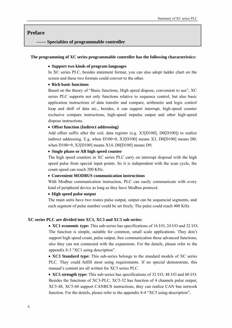
Preface —— Specialties of programmable controller
X
4
The programming of XC series programmable controller has the following characteristics:
•Is•Bsaled•Aiw•Tsc•Wk•Te
C series PL•Tsaa•Pm•BXf
Support two kinds of program languages n XC series PLC, besides statement format, you can also adopt ladder chart on the creen and these two formats could convert to the other. Rich basic functions ased on the theory of “Basic functions, High speed dispose, convenient to use”, XC
eries PLC supports not only functions relative to sequence control, but also basic pplication instructions of data transfer and compare, arithmetic and logic control oop and shift of data etc., besides, it can support interrupt, high-speed counter xclusive compare instructions, high-speed impulse output and other high-speed ispose instructions. Offset function (Indirect addressing) dd offset suffix after the coil, data register (e.g. X3[D100], D0[D100]) to realize
ndirect addressing. E.g. when D100=0, X3[D100] means X3, D0[D100] means D0; hen D100=9, X3[D100] means X14, D0[D100] means D9; Single phase or AB high speed counter he high speed counters in XC series PLC carry on interrupt disposal with the high peed pulse from special input points. So it is independent with the scan cycle, the ount speed can reach 200 KHz. Convenient MODBUS communication instructions ith Modbus communication instruction, PLC can easily communicate with every
ind of peripheral device as long as they have Modbus protocol. High speed pulse output he main units have two routes pulse output, output can be sequencial segments, and ach segment of pulse number could be set freely. The pulse could reach 400 KHz.
C are divided into XC1, XC3 and XC5 sub series: XC1 economic type: This sub-series has specifications of 16 I/O, 24 I/O and 32 I/O. he function is simple, suitable for common, small scale applications. They don’t upport high speed count, pulse output, free communication these advanced functions; lso they can not connected with the expansions. For the details, please refer to the ppendix 8-3 “XC1 using description”. XC3 Standard type: This sub-series belongs to the standard models of XC series LC. They could fulfill most using requirements. If no special demonstrate, this anual’s content are all written for XC3 series PLC.
XC5 strength type: This sub-series has specifications of 32 I/O, 48 I/O and 60 I/O. esides the functions of XC3-PLC, XC5-32 has function of 4 channels pulse output, C5-48, XC5-60 support CANBUS instructions, they can realize CAN bus network
unction. For the details, please refer to the appendix 8-4 “XC5 using description”.

Summary of XC series PLC
XC series PLC are mini type PLC with powerful function. These series products can satisfy diverse control requirement. With compact design excellent extend capability, cheap price and powerful function, XC series PLC has become perfect solution of small size control.
1. Summary of XC series PLC
1-1. Summary of XC series PLC and program format
e
1-2. XC series PLC’s model and typt
1-4. General specification
e
1-5. Shape and Sizt
1-6. Terminal arrangemen 1-7. Communication ports definition1-3. Expansion’s constitution and ID assignmen
5

Summary of XC series PLC
1-1. Summary of XC series PLC and program format XC series programmable controller I/O 14~60 points
Introduction
6
FlashROM memory inside Real time clock: With clock inside, Li battery power drop memory Multi-COM ports can connect with inverters, instruments, printers etc. Rich instructions, convenient to program
Program
Format
Alternation
Statement Program Statement program is the format which use“LD”, “AND”, “OUT”etc. These SFC instructions to input this format is the basic input form to compile the SFC program E.g: Step Instruction ID
0 LD X000 1 OR Y005 2 ANI X002 3 OUT Y005
Ladder Program Use sequencial control signal and soft unit’s ID to draw the sequencial circuit’s graph on the screen, which is called ladder program. As this method uses trigger point’s symbols and coil symbols to denote the sequencial control circuit, so it is easy to understand the program’s contents. At the same time it’s also available to monitor the PLC’s action via the status displayed in the circuit. E.g:
X0 X2
Y5
Y5
The programs compiled with the preceding two methods are both stored in the PLC’s program memory in the format of instruction table. So, the denotion and edition of this two program format can convert to the other.

Summary of XC series PLC
1-2. XC series PLC’s Model and Type
XC31 2 3 4 5
1
2
3
4
5
X
M
XC Series
Series Name XC1 series, XC3 series and XC5 series
I/O points
Input Format(NPN) R: Relay output
T: Transistor output
RT: Mix output of Transistor /Relay (Y0, Y1 are transistor)
Output Format(PNP) PR: Relay output
PT: Transistor output
PRT: Mix output of Transistor /Relay(Y0, Y1 are transistor)
Supply Power E: AC Power(220V)
C: DC Power(24V)
Clock S: With clock and RS485 COM port inside
: Without clock and RS485 COM port inside
C1 series models:
Model AC Power DC Power
Relay Output Transistor
Output Relay Output
Transistor Output
Input (DC24V)
Output (R, T)
XC3-16R-E XC3-16T-E XC3-16R-C XC3-16T-C 8 points 8 points
XC3-24R-E XC3-24T-E XC3-24R-C XC3-24T-C 12 points 12 points
N P N
Type XC3-32R-E XC3-32T-E XC3-32R-C XC3-32T-C 16 points 16 points
XC3-16PR-E XC3-16PT-E XC3-16PR-C XC3-16PT-C 8 points 8 points
XC3-24PR-E XC3-24PT-E XC3-24PR-C XC3-24PT-C 12 points 12 points
P N P
Type XC3-32PR-E XC3-32PT-E XC3-32PR-C XC3-32PT-C 16 points 16 points
ain Units
7

Summary of XC series PLC
XC3 series models:
Model AC Power DC Power
Relay Output Transistor Output
Mix output (R&T)
Relay Output Transistor Output
Mix output (R&T)
Input (DC24V)
Output (R, T)
XC3-14R-E XC3-14T-E XC3-14RT-E XC3-14R-C XC3-14T-C XC3-14RT-C 8 points 6 points
XC3-24R-E XC3-24T-E XC3-24RT-E XC3-24R-C XC3-24T-C XC3-24RT-C 14 points 10 pointsXC3-32R-E XC3-32T-E XC3-32RT-E XC3-32R-C XC3-32T-C XC3-32RT-C 18 points 14 pointsXC3-48R-E XC3-48T-E XC3-48RT-E XC3-48R-C XC3-48T-C XC3-48RT-C 28 points 20 points
N P N
Type XC3-60R-E XC3-60T-E XC3-60RT-E XC3-60R-C XC3-60T-C XC3-60RT-C 36 points 24 points
XC3-14PR-E XC3-14PT-E XC3-14PRT-E XC3-14PR-C XC3-14PT-C XC3-14PRT-C 8 points 6 points XC3-24PR-E XC3-24PT-E XC3-24PRT-E XC3-24PR-C XC3-24PT-C XC3-24PRT-C 14 points 10 points
XC3-32PR-E XC3-32PT-E XC3-32PRT-E XC3-32PR-C XC3-32PT-C XC3-32PRT-C 18 points 14 pointsXC3-48PR-E XC3-48PT-E XC3-48PRT-E XC3-48PR-C XC3-48PT-C XC3-48PRT-C 28 points 20 points
P N P
Type XC3-60PR-E XC3-60PT-E XC3-60PRT-E XC3-60PR-C XC3-60PT-C XC3-60PRT-C 36 points 24 points
XC5 series models:
Model AC Power DC Power
Relay Output Transistor
Output Mix output
(R&T) Relay Output
Transistor Output
Mix output (R&T)
Input (DC24V)
Output (R, T)
- XC5-32T-E XC5-32RT-E - XC5-32T-C XC5-32RT-C 18 points 14 points
XC5-48R-E XC5-48T-E XC5-48RT-E XC5-48R-C XC5-48T-C XC5-48RT-C 28 points 20 points
N P N
Type XC5-60R-E XC5-60T-E XC5-60RT-E XC5-60R-C XC5-60T-C XC5-60RT-C 36 points 24 points
- XC5-32PT-E XC5-32PRT-E - XC5-32PT-C XC5-32PRT-C 18 points 14 points
XC5-48PR-E XC5-48PT-E XC5-48PRT-E XC5-48PR-C XC5-48PT-C XC5-48PRT-C 28 points 20 points
P N P
Type XC5-60PR-E XC5-60PT-E XC5-60PRT-E XC5-60PR-C XC5-60PT-C XC5-60PRT-C 36 points 24 points
8

Summary of XC series PLC
XC1 2 3 4
E5 6
1. Series name 2. E: Expansion
5. Output points 6. Output format YR: Relay output YT: Transistor output
Model
3. Input points 4. X: Input
Input R Ou t
I/O Input
(DC V) Output
elay Output Transistor tpu
points 24 (R, T)
- XC-E8YR XC-E8YT 8 points - 8 points XC-E16X - - 16 points 16 points -
- XC-E16YR XC-E16YT 16 points - 16 points - XC-E 8YR XC-E 8YT 8 p s 8X 8X 16 points 8 points oint X XC-E1 16YT 16 p ts C-E16X16YR 6X 32 points oin 16 points
XC-E32X - - 32 points 32 points - - XC-E32YR - 32 points - 32 points
Digital I/O Expansions
9
Summary of XC series PLC
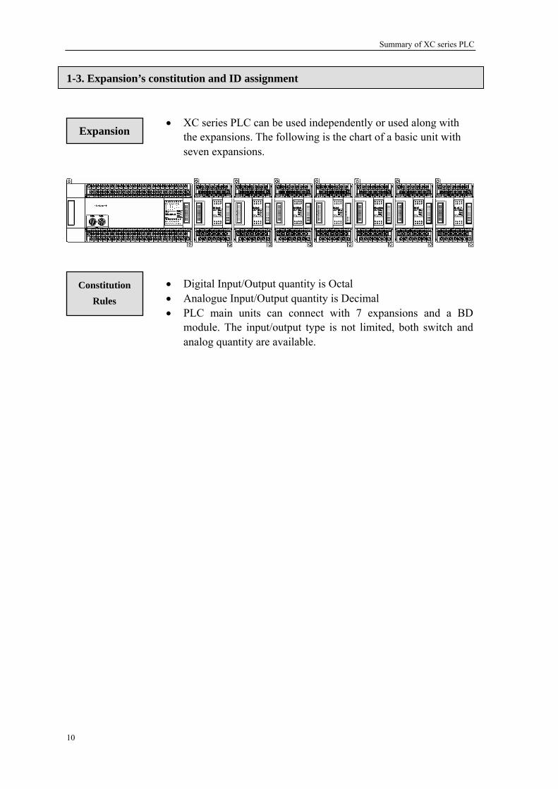
• XC series PLC can be used independently or used along with the expansions. The following is the chart of a basic unit with seven expansions.
• Digital Input/Output quantity is Octal • Analogue Input/Output quantity is Decimal • PLC main units can connect with 7 expansions and a BD
module. The input/output type is not limited, both switch and analog quantity are available.
1-3. Expansion’s constitution and ID assignment
Expansion
Constitution Rules
10

Summary of XC series PLC
Unit Type ID(As register) Max points/
Channels
Input switch quantity X X100~X137 32 points
Output switch quantity Y Y100~Y137 32 points
Input analog quantity ID ID100~ID131 16 channels
Output analog quantity QD QD100~QD131 16 channels
Expansion
1#
Module’s set value D D8250~D8259 -
Input switch quantity X X200~X237 32 points
Output switch quantity Y Y200~Y237 32 points
Input analog quantity ID ID200~ID231 16 channels
Output analog quantity QD QD200~QD231 16 channels
Expansion
2#
Module’s set value D D8260~D8269 -
Input switch quantity X X300~X337 32 points
Output switch quantity Y Y300~Y337 32 points
Input analog quantity ID ID300~ID331 16 channels
Output analog quantity QD QD300~QD331 16 channels
Expansion
3#
Module’s set value D D8270~D8279 -
Input switch quantity X X400~X437 32 points
Output switch quantity Y Y400~Y437 32 points
Input analog quantity ID ID400~ID431 16 channels
Output analog quantity QD QD400~QD431 16 channels
Expansion
4#
Module’s set value D D8280~D8289 -
Input switch quantity X X500~X537 32 points
Output switch quantity Y Y500~Y537 32 points
Input analog quantity ID ID500~ID531 16 channels
Output analog quantity QD QD500~QD531 16 channels
Expansion
5#
Module’s set value D D8290~D8299 -
Input switch quantity X X600~X637 32 points
Output switch quantity Y Y600~Y637 32 points
Input analog quantity ID ID600~ID631 16 channels
Output analog quantity QD QD600~QD631 16 channels
Expansion
6#
Module’s set value D D8300~D8309 -
Input switch quantity X X700~X737 32 points
Output switch quantity Y Y700~Y737 32 points
Input analog quantity ID ID700~ID731 16 channels
Output analog quantity QD QD700~QD731 16 channels
Expansion
7#
Module’s set value D D8310~D8319 -
Input switch quantity X X1000~X1037 32 points
Output switch quantity Y Y1000~Y1037 32 points
Input analog quantity ID ID1000~ID1031 16 channels
Output analog quantity QD QD1000~QD1031 16 channels
BD Board
Module’s set value D D8320~D8329 -
ID Assignment
11

Summary of XC series PLC
1-4. General Specification
InsuA
teAmb
In
G
General Specification
12
Items Specifications late voltage Up to DC 500V 2MΩ nti-noise 1000V 1uS pulse per minute
Ambient mperature
0°C~60°C
ient humidity 5%~95% COM 1 RS-232, connect with host machine, HMI program or debug COM 2 RS-232/RS-485, connect with network or aptitude instrument,
inverters etc. COM 3 BD board COM port RS-232C/RS-485 COM 4 CANBUS COM port (XC5 series) stallation Can use M3 screw to fix or install directly on DIN46277
(Width 35mm) orbit rounding The third type grounding (can’t public ground with strong
power system.)

Summary of XC series PLC
XC3 series:
Performance
Specification Item 14 points 24/32 points 48/60 points
Program executing format
Loop scan format, time scan format
Program format Both statement and ladder Dispose speed 0.5us
Power cut retentive Use FlashROM and Li battery User program’s capacity 2500 steps 8000 steps
I/O points 8 I / 6 O Input 14/18 pointsOutput 10/14
points
Input 28/36 points Output 20/24 points
Interior coil’s points (M) 8512 points Points 620 points
Timer (T) Spec.
100mS timer: Set time 0.1~3276.7 seconds 10mS timer: Set time 0.01~327.67 seconds 1mS timer: Set time 0.001~32.767 seconds
Points 635 points Counter
(C) Spec. 16 bits counter: set value K0~32767 32 bits counter: set value K0~2147483647
Data Register(D) 8512 words FlashROM Register(FD) 2048 words
High speed dispose function
High speed count, pulse output, external interrupt
Setting of time scan space
0~99mS
Password protection 6 bits ASCII Self diagnose function Power on self-diagnose, Monitor timer, grammar check
13

Summary of XC series PLC
1-5. Shape and Size
Exterior Size
XC1 series 16 points main units XC3 series 14 points main units (Including 16 points expansions)
XC1 series 32 points main units (Including 24 points main units) XC3 series 24 / 32 points main units (Including 32 points expansions) XC5 series 32 points main units
10 4 5326 7
76
XC3-32R-EERR
RUN
2 3 540 1
73.3
Xinje Electronic Co.,Ltd
SN:0067032266DATE:20060410TYPE:XC3-32R-E
0V24V B
AY0
COM0Y1
COM1Y2
COM2 Y3Y4
Y10 COM4Y11
Y6Y7
Y5COM3 Y12
Y13Y14
Y15
PORT2PORT1
139
102
94
131
X
Y
PWR
X21X20
X17X10
X11X12
X13X14 X16
X15X7X6
X5X4
X3X2
X1X0COM
COMFG
110
3.5
14

Summary of XC series PLC
XC3 series 60 points main units (Including 48 points main units) XC5 series 60 points main units (Including 48 points main units)
COM9COM8
199.4
102
73.3
207.4
94
Xinje Electronic Co.,Ltd
SN:0067032266DATE:20060410Y
X
X0X1COM
COM X2X3
X4X5
X6X7
X10X11
X12X13
X14X15
X16X17
X20X21
X22X23
X24X25
X26X27
X30X37
X40X36X35
X34X33
X32X31 X41
X42X43
Y27Y26
Y25Y24
Y15 Y17COM6 Y21
Y20COM7Y23
Y22Y16Y13 Y14
COM5Y11
Y12Y7 Y10Y6COM4
Y4Y5COM3
Y3Y2Y1COM2
Y0COM1COM0
CAN+ CAN-A B
0V24V
PORT2PORT1 ERRRUNPWR
0 1 32 6 754
4 5 762 310
XC3-60R-E
TYPE:XC3-60R-E
15

Summary of XC series PLC
1-6. Terminal arrangement
16
Main Units
1. Input terminals 2. BD expansion 3. Input label 4. COM port 5. COM port 6. COM port’s cover door 7. Output label 8. Output terminals 9. Screws 10. Input indicate LED 11. Extension port 12. Programming status indicate LED 13. Output indicate LED
Summary of XC series PLC
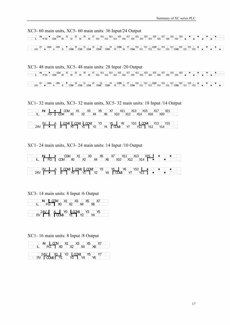
XC3- 60 main units, XC5- 60 main units: 36 Input/24 Output
Y12 COM7Y7COM4
X31X32
X33X30
X27X26
X25X24
X23X22
X21X20
X17X16
X15X14
X13X12
X11X10
X7X6
X5X4
X3X2COM
COM
0V24V A
CAN+B
CAN-COM0 COM1
Y0COM2
Y1 Y2COM3
Y3Y5
Y4Y6
COM5COM6 Y11
Y10Y13 Y14 Y16
Y22Y23
Y20Y21
Y17COM8
Y15
X1X0
XC3- 48 main units, XC5- 48 main units: 28 Input /20 Output
Y12 COM7Y7COM4
X31X32
X33X30
X27X26
X25X24
X23X22
X21X20
X17X16
X15X14
X13X12
X11X10
X7X6
X5X4
X3X2COM
COM
0V24V A
CAN+B
CAN-COM0 COM1
Y0COM2
Y1 Y2COM3
Y3Y5
Y4Y6
COM5COM6 Y11
Y10Y13 Y14 Y16
Y20Y2
Y17COM8
Y15 Y22Y231
X1X0
C1- 32 main units, XC3- 32 main units, XC5- 32 main units: 18 Input /14 Output X
FGCOM X1 X3 X5 X7 X1X13X11
COM X0 X2 X4 X65
X16X14X12X10X17
X20X21
Y15Y14
Y13Y12COM3
Y5Y7
Y6Y11
COM4Y10Y4
Y3COM2Y2
COM1Y1
COM0Y0
AB24V
0V
C1- 24 main units, XC3- 24 main units: 14 Input /10 Output X
0V24V B
AY0
COM0Y1
COM1Y2
COM2 Y3Y4
Y10Y11
Y6Y7
Y5COM3
X10X11
X12X13
X14X15X7
X6X5
X4X3
X2X1
X0COMCOM
FG
XC3- 14 main units: 8 Input /6 Output
COMFG
X1 X3 X5 X7X6X4X2X0
24V Y0 COM1 Y3 Y5Y4Y2Y1COM0B0V
A
XC1- 16 main units: 8 Input /8 Output
COMFG
X1 X3 X5 X7X6X4X2X0
24V Y0 COM1Y2 Y7Y4Y3Y1COM00V
Y5Y6
17
Summary of XC series PLC
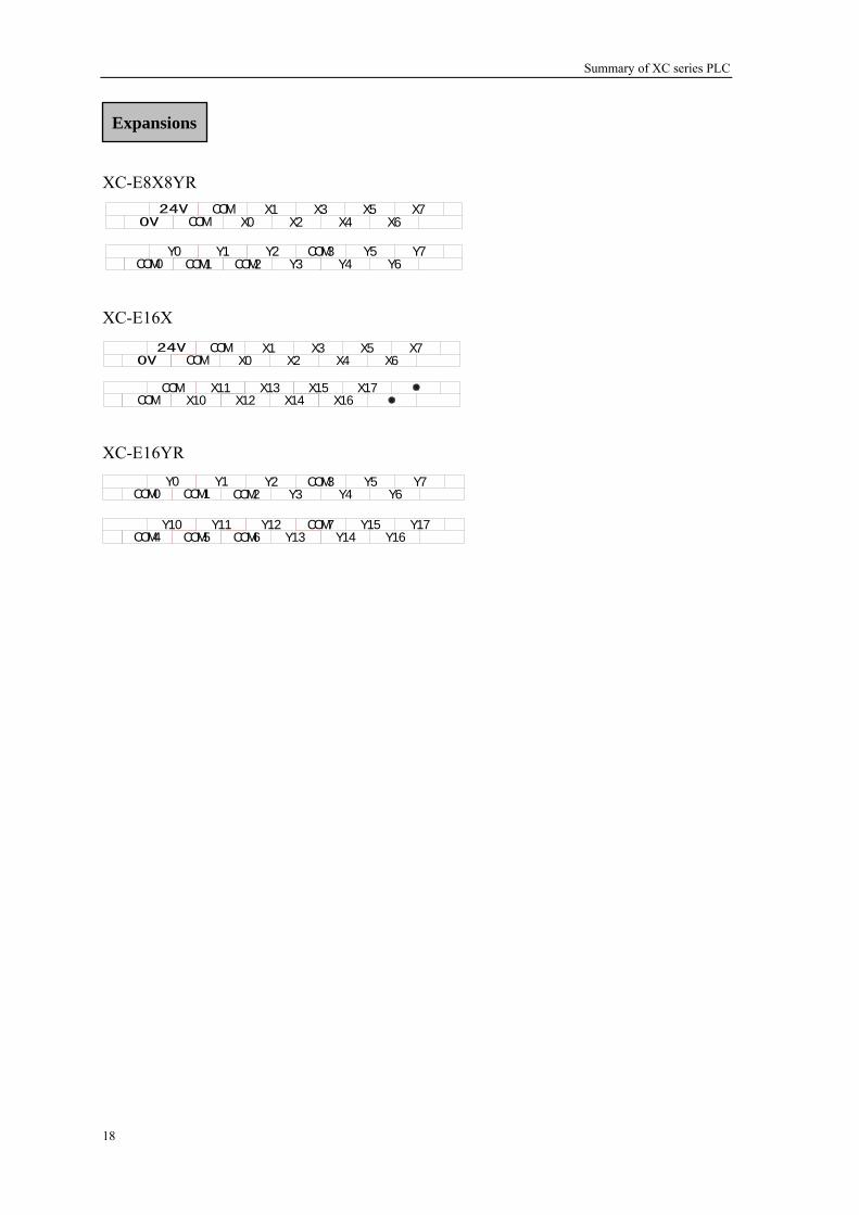
Expansions
XC-E8X8YR
COM
Y1COM0
Y0COM1 COM2 Y3 Y4 Y6
Y7Y5COM3Y2
X0 X2 X4 X6X7X5X3X1COM
XC-E16X
COM X1 X3 X5 X7X6X4X2X0
COMCOM
X13 X15 X17X16X14X12X10
X11
COM
XC-E16YR
Y0COM0 COM1
Y11COM4 COM5 COM6 Y13 Y14 Y16
Y17Y15COM7Y12Y10
COM2 Y3 Y4 Y6Y7Y5COM3Y2Y1
18

Summary of XC series PLC
1-7. COM Port Definition
COM 1
COM 2
PRG RxD TxD VCC GND
备注
Pin of COM 1
3 4 5
1 2
6 87
Mini Din 88 core socket (hole)
2: 4: 5: 6: 8:
RxD TxD GND
Pin of COM 2
3 4 5
1 2
6 87
Mini Din 88 core socket (hole)
4: 5: 8:
Connection of programmable cable is the following:
19
345
12
687
15
9 6 Mini Din 8 core socket (pin) DB9 pin (hole)


2-1. Power Specification For the power specification of XC series programmable controller’s basic units, please see the following table:
AC Power Type
Rated voltage AC100V~240V Voltage allow bound AC90V~265V Rated frequency 50/60Hz Allow momentary power-cut time
Interrupt time≤0.5 AC cycle, alternation≥1 sec
Impact current Max 40A 5mS below/AC100V max 60A 5mS below /AC200V
Max power consumption
12W
Power for sensor use 24VDC±10% max 400mA
• To avoid voltage decrease, please use the power cable thicker than 2mm2
• Even appear power cut within 10ms; PLC can still go on working. But if long time power cut or abnormal power decrease, PLC will stop working, output will also appear OFF status, when recover power supply, the PLC will auto start to work.
• Connect the grounding terminals of basic units and extend modules together, then ground
DC power type
Rated voltage DC24V
Voltage allow bound DC21.6V~26.4V
Input current (Only basic unit)
120mA DC24V
Allow momentary power-cut time
10mS DC24V
Impact current 10A DC26.4V
Max power consumption
12W
Power for sensor use
24VDC±10% Max 400mA
21

Spec., Input/output and layout
2-2. AC Power, DC Input Type
Constitution and
Connection
·
·
• The Input power is connected between L and N terminals. • 24+, COM terminals can be used to power 400mA/DC24V for sensor
supply. Besides, this terminal can’t be connected to external power. • Terminal is NC terminal, please don’t go on exterior connection or
use it as relay terminal. • Connect the basic unit with all expantions module’s COM terminal.
22
Spec., Input/output and layout
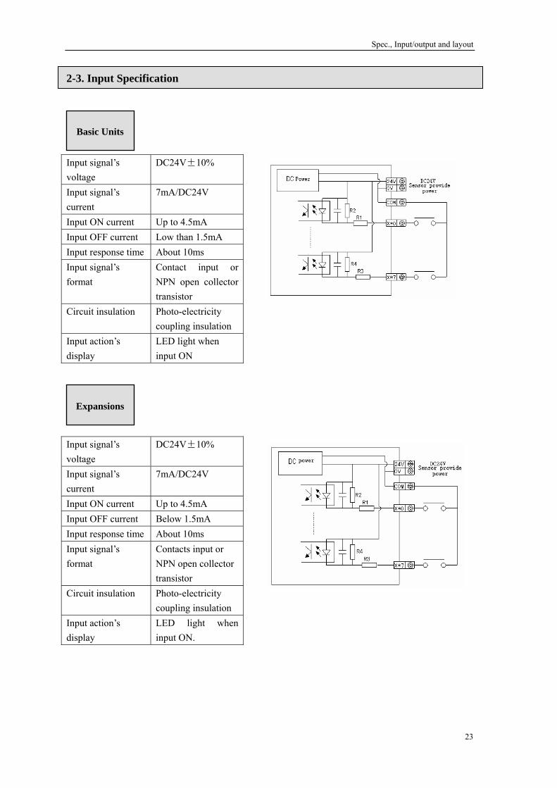
2-3. Input Specification
Input signal’s voltage
DC24V±10%
Input signal’s current
7mA/DC24V
Input ON current Up to 4.5mA Input OFF current Low than 1.5mA Input response time About 10ms Input signal’s format
Contact input or NPN open collector transistor
Circuit insulation Photo-electricity coupling insulation
Input action’s display
LED light when input ON
Basic Units
Expansions
Input signal’s voltage
DC24V±10%
Input signal’s current
7mA/DC24V
Input ON current Up to 4.5mA Input OFF current Below 1.5mA Input response time About 10ms Input signal’s format
Contacts input or NPN open collector transistor
Circuit insulation Photo-electricity coupling insulation
Input action’s display
LED light when input ON.
23
Spec., Input/output and layout
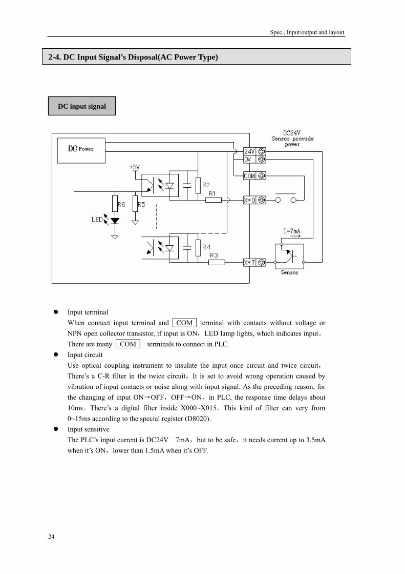
2-4. DC Input Signal’s Disposal(AC Power Type)
Input terminal When connect input terminal and COM terminal with contacts without voltage or NPN open collector transistor, if input is ON,LED lamp lights, which indicates input。There are many COM terminals to connect in PLC.
Input circuit Use optical coupling instrument to insulate the input once circuit and twice circuit,There’s a C-R filter in the twice circuit。It is set to avoid wrong operation caused by vibration of input contacts or noise along with input signal. As the preceding reason, for the changing of input ON→OFF,OFF→ON,in PLC, the response time delays about 10ms。There’s a digital filter inside X000~X015。This kind of filter can very from 0~15ms according to the special register (D8020).
Input sensitive The PLC’s input current is DC24V 7mA,but to be safe,it needs current up to 3.5mA when it’s ON,lower than 1.5mA when it’s OFF.
DC input signal
24

Spec., Input/output and layout
XC series PLC’s input power is supplied by its interior 24V power,so if use exterior power to drive photoelectricity sensor etc., this exterior power should be DC24V±4V,please use NPN open collector type for sensor’s output transistor
Exterior
circuit used
Input Connection
25

Spec., Input/output and layout
2-5. Output Specifica
low AC250V, DC30V
tion
Interior power BeCircuit insulation ion Mechanism insulatAction deno mp te LED indicate la
Resistant load
3A
Induce load 80VA
Max load
Lamp load 100W Open circuit’s leak
current -
Mini load DC5V 2mA OFF→ON 10ms Response
me ON→OFF 10ms ti
Interior power Below DC5~30V
Relay output
Transistor Output
Circuit insulation Optical coupling insulation
Action denote Indicate lamp LED Restance load
0.8A
Induce load 12W/DC24V
Max load
Lamp load 1.5W/DC24V Open circuit’s leak urrent
- cMini load DC5V 2mA
OFF→ON Below 0.2ms Response time ON→OFF Below 0.2ms
26
Spec., Input/output and layout
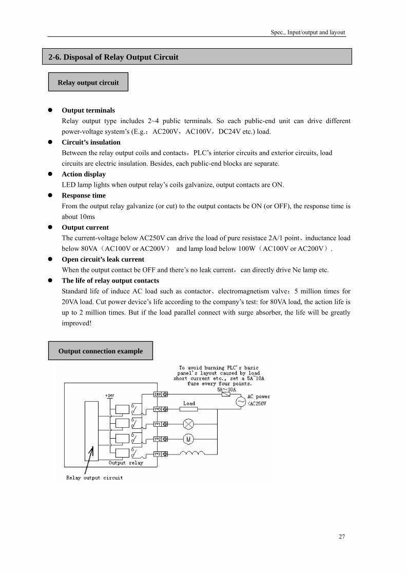
2-6. Disposal of Relay Output Circuit
Output terminals Relay output type includes 2~4 public terminals. So each public-end unit can drive different power-voltage system’s (E.g.:AC200V,AC100V,DC24V etc.) load.
Circuit’s insulation Between the relay output coils and contacts,PLC’s interior circuits and exterior circuits, load circuits are electric insulation. Besides, each public-end blocks are separate.
Action display LED lamp lights when output relay’s coils galvanize, output contacts are ON.
Response time From the output relay galvanize (or cut) to the output contacts be ON (or OFF), the response time is about 10ms
Output current The current-voltage below AC250V can drive the load of pure resistace 2A/1 point、inductance load below 80VA(AC100V or AC200V) and lam load below 100W(AC100V or AC200V).
Open circuit’s leak current When the output contact be OFF and there’s no leak current,can directly drive Ne lamp etc.
The life of relay output contacts Standard life of induce AC load such as cont ctor、electromagnetism valve:5 million times for 20VA load. Cut power device’s life according t the company’s test: for 80VA load, the action life is up to 2 million times. But if the load parallel nnect with surge absorber, the life will be greatly improved!
Relay output circuit
Output connection example
p
aoco
27

Spec., Input/output and layout
Constitution of output
circuit
For DC induce load, please parallel connect with commutate diode. If not connect with the commutate diode, the contact’s life will be decreased greatly. Please choose the commutate diode which allow inverse voltage endurance up to 5~10 times of the load’s voltage, ordinal current exceeds load current.
Parallel connect AC induce load with surge absorber can reduce noise.
DC load
AC load
28

Spec., Input/output and layout
29
2-7. Disposal of Transistor Output Circuit
Output terminal Basic unit’s transistor output has 1~4 public-end output.
Exterior power Please use DC5~30V steady-voltage power for load drive,
Circuit insulation Use photoelectricity coupling device to insulate PLC’s interior circuit and output transistor. Besides, each public block is separate.
Action denote When drive optical coupling,LED lights,output transistor is ON.
Response time From photoelectricity coupling device drive (or cut) to transistor ON (or OFF), the time PLC uses is below 0.2ms.
Output current The current is 0.5A per point。But as restrict by temperature goes up, the current is 0.8A every four points.
Open circuit’s current Below 0.1mA
Transistor output circuit


3. Each Soft Unit’s Usage and Function T his chapter, we’ll give some description of the PLC’s data and the function of interior input/output relay, auxiliary
lay, status, counter, data register etc. This item is the base to use PLC. re
3-1.Every Soft Unit of PLC
3-2.Soft Unit’s ID List
3-3.Disposal of Data
3-4.Some Encode Principle of Soft Units
3-5.Timer’s ID and Function [T]
3-6.Counter’s ID and Function [C]
3-7.Note Items
31
Function of each device
3-1. Every Soft Unit of Programmable Controller
In the programmable controller, there are many relays、timers and counters,they all have countless “a” contacts(Normally open contacts)and “b” contacts(Normally closed contacts),Connect these contacts and coils to constitute sequencial control circuit. The following, we’ll briefly introduce each soft unit:
In each basic unit,assign the ID of input relay, output relay in the format of X000~X007,X010~X017…,Y000~Y007,Y010~Y017… this octal format. The ID of extension is connected behind basic unit.
The ID of expansion obeys the principle of channel 1 starts from X100/Y100, channel 2 starts from X200/Y200… 7 expansions could be connected totally.
Use digital filter in the special input filter of input relay, so you can use the program to change the sieve value. So in the high-speed receive application, you can assign this type of relay’s ID No.
Auxiliary relay is the relay inside the programmable controller,this type of output relay is different from input/output relay,it can’t gain exterior input,it also can’t drive exterior load,it can only be used in the program。
The relay used for retentive can still save its ON/OFF status in the case of PLC power cut.
Relay used as step ladder chart. When not used as working procedure No.,it’s the same with auxiliary relay and can be
used as common contact/coil to carry on programming. Besides, it can also be signal alarm to diagnose exterior trouble.
Timer could carry on plus operation to 1ms,10ms,100ms etc. time pulse in PLC, When reach certain set value, output contact act.
T100~T199 are timers with the unit of 100ms clock pulse,their current values are the accumulate values. So, even though timer coil’s drive input is cut, they will still hold the current value, go on accumulating the action.
【Auxiliary relay(M)】
【Timer(T)】
【Status(S)】
【Input(X)and output(Y)relay】
32

Function of each device
The counters can be divided into the following sorts according the their usage and purpose: [Used for interior count] Common use / power failure retentive use 16 bits counter:Used for plus count,count bound: 1~32,767 32 bits counter:Used for add / minus count,count bound: -2,147,483,648~+2,147,483,647
These counters are used for PLC’s interior signals, usually their response speed is below 10Hz.
[Used for high-speed count] For power failure retentive use 32 bits counter: For plus / minus count, count bound: -2,147,483,648~+2,147,483,6487
(Single phase plus count,single phase plus/minus count,AB phase count) allocate to the special input points.
High-speed counter can count with the frequency below 200kHz,independent with the PLC’s scan cycle.
【Counter(C)】
Data register is the soft unit used by data register to save data. XC series PLC’s data registers are all 16 bits (The high bit is the sign bit), Combine two registers can carry on 32 bits data disposal (The high bit is the sign bit). Just the same with other soft units, data registers can also be divided to be two types: for common use and power failure retentive use.
【Data register(D)】
In the diverse value used by PLC, K means decimal integer,H means Hex. Value. They are used to be the set value and current value for the timer and counter, or applied instructions’ operands.
【Constant(K)、(H)】
【Pointer(P)(I)】
Pointers are used for branch and interrupt. The pointer (P) used by branch is the jump aim used for condition jump or subroutine jump. Pointer used for interrupt is used for the assigned input interrupt, time interrupt.
33
Function of each device
3-2. Device’s ID List
For the allocate of device’s ID, please see the following list: Besides, when connect input / output expansions and special expansions on the basic units, for the input / output relay’s No., please refer to the user manual.
Bound points Mnemonic Name
14 points 24\32 points 48 \60 points 14
points 24\32 points
48 \60 points
X Input relay X000~X007 X000~X015 X000~X021
X000~X033 X000~X043
8 points 14\18 points
28\36 points
Y Output relay Y000~Y005 Y000~Y011 Y000~Y015
Y000~Y023 Y000~Y027
6 points 10\14 points
20\24 points
M0~M2999【M3000~M7999】 8000 M Interior relay
M8000~M8511 for special using 512
S Flow S0~S511
【S512~S1023】 1024
T0~T99:100ms not accumulation T100~T199:100ms accumulation T200~T299:10ms not accumulation T300~T399:10ms accumulation T400~T499:1ms not accumulation T500~T599:1ms accumulation
T Timer
T600~T618:1ms with interruption precise time
620
C0~C299:16 bits forth counter C300~C598:32 bits forth/back counter C Counter C600~C634:high-speed counter
635
D0~D3999 【D4000~D7999】
8000 D Data Register
For special usage D8000~D8511 512
FD0~FD1535 1536 FD
FlashROM Register
For special usage FD8000~FD8511 512
34

Function of each device
NOTE: ※1. The memorizer area in 【 】 is the defaulted power failure retentive area;soft
elements D、M、S、T、C can be set to change the power failure retentive area. For the details, please see the following table
※2. FlashROM register needn’t set power failure retentive, its data won’t lose when power is cut (No battery).
※3. The serial No. of input coil、output relay are octal data, other memorizers’ No. are all algorism data.
Setting of soft unit’s power failure saving area:
Mnemonic Set area Function System’s defaulted
value
Memory bound of power drop
D FD8202 Start denotation of D power
cut save area 4000 D4000~D8000
M FD8203 Start denotation of M power
cut save area 3000 M3000~M8000
T FD8204 Start denotation of T power
cut save area 620 Not set
C FD8205 Start denotation of C power
cut save area 320 C320~C640
S FD8206 Start denotation of S power
cut save area 512 S512~S1024
35
Function of each device
3-3. Data Disposal of Programmable Controller
According to different usage and purpose, XC series programmable controllers use 5 types of count format. For their usage and function, see the following:
《DEC》(DEC:DECIMAL NUMBER) The set value of timer and counter(K constant) The ID of auxiliary relay(M),timer(T),counter(C),status(S)(Soft
unit’s number) Assign the value in the operands and instruction’s action(K constant)
《HEX》(HEX:HEXADECIMAL NUMBER) The same with DEC data,it is used to assign the value in the operands and
instruction’s action(H constant)
《OCT》(OCT:OCTAL NUMBER) The input relay, output relay’s soft units’ ID of XC series PLC are allocate in
the format of OCT data. So, it can go on carry of [1-7,10-17,...70-77,100-107].
《BCD code》(BCD: BINARY CODE DECIMAL) BCD is the method which use 4 bits binary to denote decimal 0~9. It’s easy to
despose bit. So, BCD is available to denote digital switch or 7 segments display control.
《Other data(float)》 XC series PLC has the function of high precision floating point operation. Use binary
floating point data to execute floating point operation, use decimal floating value to execute monitor.
《BIN》(BIN:BINARY NUMBER) Just as said before,carry on data allocation to timer, counter or data register in
the format of DEC. or Hex., But in the PLC, these data are all be put in the format of binary data. And, when carry on monitor on the peripherial device, these soft units will auto switch to be DEC. data as shown in the graph.(they can also switch to be Hex. Data.).
36
Function of each device
3-4. Some encode principles of device
MOV D10[D0] D100M8000
M2
Y0[D0]
MOV K5 D0
M8002MOV K0 D0
MOV K21 DY0M0
MOV K3 D0M1
MOV DX2[D0] D10M8000
1、Data register could be used as offset(indirect assignment) Format:Dn[Dm]、Xn[Dm] 、Yn[Dm] 、Mn[Dm] etc.
2、 Bit units compose word Input X、output Y、middle coil M could compose 16 bits word. E.g. DX0 means X0~X17compose to be a 16 bits data. DX20 means X20~X37 combines a 16 bits data. Format:Add a D before bit device
Bit devices combine to be word devices:DX、DY、DM、DS、DT、DC
In the preceding example, when D0=0, then D100=D10, Y0 is ON; When M2 turns from OFF to be ON, D0=5, then D100=D15, Y5 is ON. When D10[D0]=D[10+D0], Y0[D0]=Y[0+D0].
Word’s offset composed by bit soft units:DXn[Dm] means DX[n+Dm]; Soft units with offset, the offset could only be denoted with soft device D.
In the preceding example, when M0 turns from OFF to be ON, the value of the word DY0 composed by Y0~Y17 equals 21,i.e. Y0、Y2、Y4 turns to be ON status.
Before M1 be activate, when D0=0, DX2[D0] means a word composed by X2~X21; When M1turns from OFF to be ON, D0=3, then DX2[D0] means a word composed by X5~X24
DXn(the bound of “n” is the exact bound of “X”),choose 16 points from the head to the end, add 0 if not enough.
Please note, the word composed by bit device couldn’t carry on bit searching address.
37
Function of each device
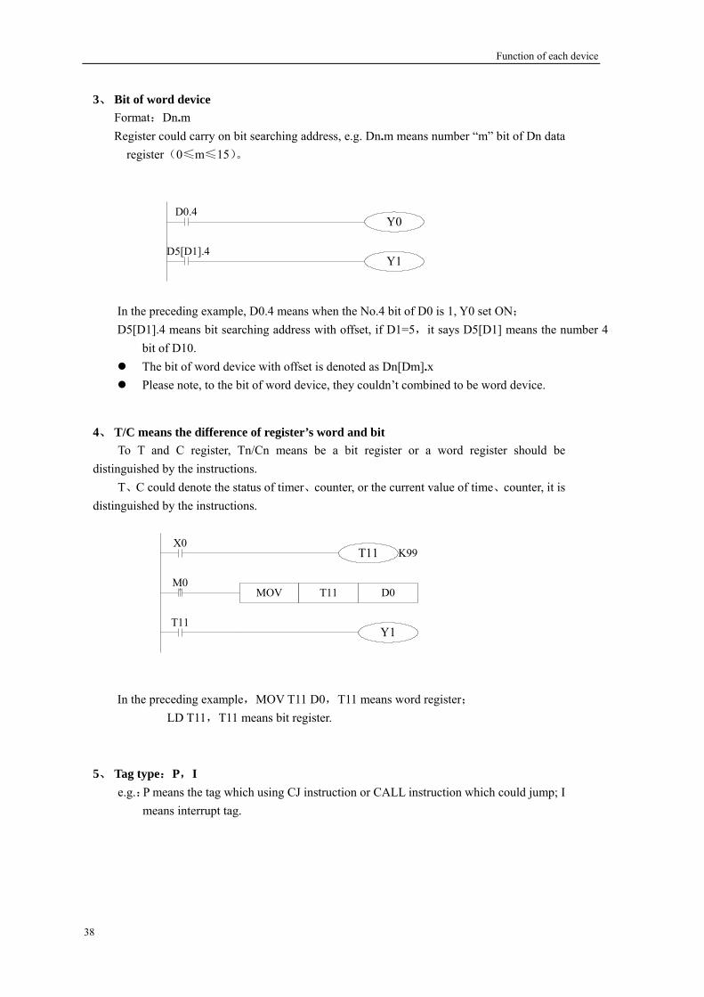
D0.4Y0
D5[D1].4Y1
MOV D0T11M0
T11Y1
X0T11 K99
5、 Tag type:P,I
e.g.:P means the tag which using CJ instruction or CALL instruction which could jump; I means interrupt tag.
3、 Bit of word device Format:Dn.m Register could carry on bit searching address, e.g. Dn.m means number “m” bit of Dn data
register(0≤m≤15)。
4、 T/C means the difference of register’s word and bit To T and C register, Tn/Cn means be a bit register or a word register should be
distinguished by the instructions. T、C could denote the status of timer、counter, or the current value of time、counter, it is
distinguished by the instructions.
In the preceding example, D0.4 means when the No.4 bit of D0 is 1, Y0 set ON; D5[D1].4 means bit searching address with offset, if D1=5,it says D5[D1] means the number 4
bit of D10. The bit of word device with offset is denoted as Dn[Dm].x Please note, to the bit of word device, they couldn’t combined to be word device.
In the preceding example,MOV T11 D0,T11 means word register; LD T11,T11 means bit register.
38

Function of each device
3-5. Timer’s Number and Function [T]
100ms not accumulated(16 bits) T0~T99 100ms accumulated(16 bits) T100~T199 10ms not accumulated(16 bits) T200~T299 10ms accumulated(16 bits) T300~T399 1ms not accumulated(16 bits) T400~T499 1ms accumulated(16 bits) T500~T599
Timer’s number Please see the following table for the timer’s [T] number (the number is assigned according to Hex.)
Function The timer accumulates clock pulse of 1ms,10ms,10ms inside PLC. When reach the set value, the output contact activates. The common timers don’t set exclusive instructions, use OUT instruction to time; use constant K in the program memory, also you could use register’s content (D) to indirect assign.
If the drive input X001 of timer’s coil T300 is ON, T300 accumulates 10ms clock pulse with the current value counter. When the value reaches the set value K2000, counter’s output contact activates. In the count process, even the input X001 cut or drop power, when start again, go on counting, its accumulation time is 20 seconds. When reset input X002 is ON, timer reset, output contact reset.
If drive input X000 of time coil T200 is ON, T200 accumulates 10ms clock pulse with the current value timer. If this current value equals the set value K200, timer’s output contact activates. That is, output contact activates after 2 seconds of coil driving. Driving input X000 cut or power cut, timer reset, output contact reset.
Com
mon form
at A
ccumulation form
at
39

Function of each device
T10 K100X0
MOV K200 D5
T10 D5
X0
X1
Y0
T2
X0
Y0 X0X0
Y0 T2K200
T2
T1
T2
Y0
X0
T1
T2
X0
Y0T1 T2 T1K10
K20
T10 is a timer with the unit of
100ms. Assign 100 as a constant,
then 0.1s×100=10s timer work.
Write content in indirect data register
to program or input via data switch.
When assigned as power cut retentive
register, please note that voltage low
will cause the set value instable.
《Output delay on-off timer》
Action
《Flicker》
《Constant assignment (K)》
《Indirect assignment (D)》
Assign method of
the set value
If X000 activates, Y000 starts flicker output. T1 controls the OFF time of Y000, T2 controls the ON time of Y000.
When X000 is ON, output Y000; If X000 changes from ON to be OFF, T2(20 seconds)will be delayed, the will output Y000 cut.
The Time
Value
The count format of Timers T0~T599 is 16 bits linear increment mode (0~K32 ,767). If the timer’s count value reaches the maximum value K32767, the timer will stop timing , the timer’s status will remain the same status.
n
40
Function of each device
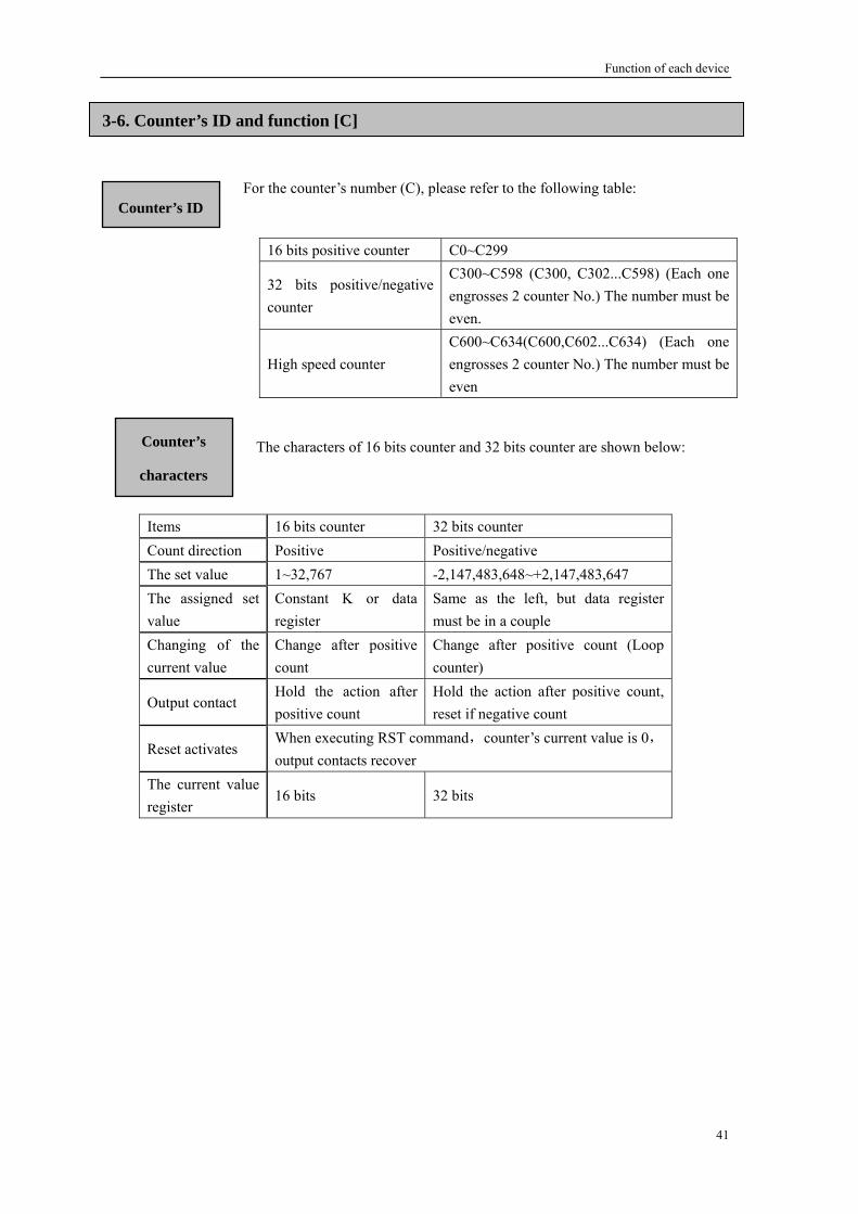
3-6. Counter’s ID and
16 bits positive counter 299
function [C]
C0~C
32 bits positive/negative counter
C300~C598 (C300, C302...C598) (Each one engrosses 2 counter No.) The number must be even.
High speed counter C600~C634(C600,C602...C634) (Each one engrosses 2 counter No.) The number must be even
Counter’s ID For the counter’s number (C), ple r to the following table: ase refe
Counter’s
characters
The characters of 16 bits counter and 32 bits counter are shown below:
Items 16 bits counter 32 bits counter Count direction Positive Positive/negative The set value 1~32,767 -2,147,483,648~+2,147,483,647 The assigned set value
Constant K or data register
Same as the left, but data register must be in a couple
Changing of the current value
Change after positive count
Change after positive count (Loop counter)
Output contact Hold the action after positive count
Hold the action after positive count, reset if negative count
Reset activates When executing RST command,counter’s current value is 0,output contacts recover
The current value register
16 bits 32 bits
41
Function of each device
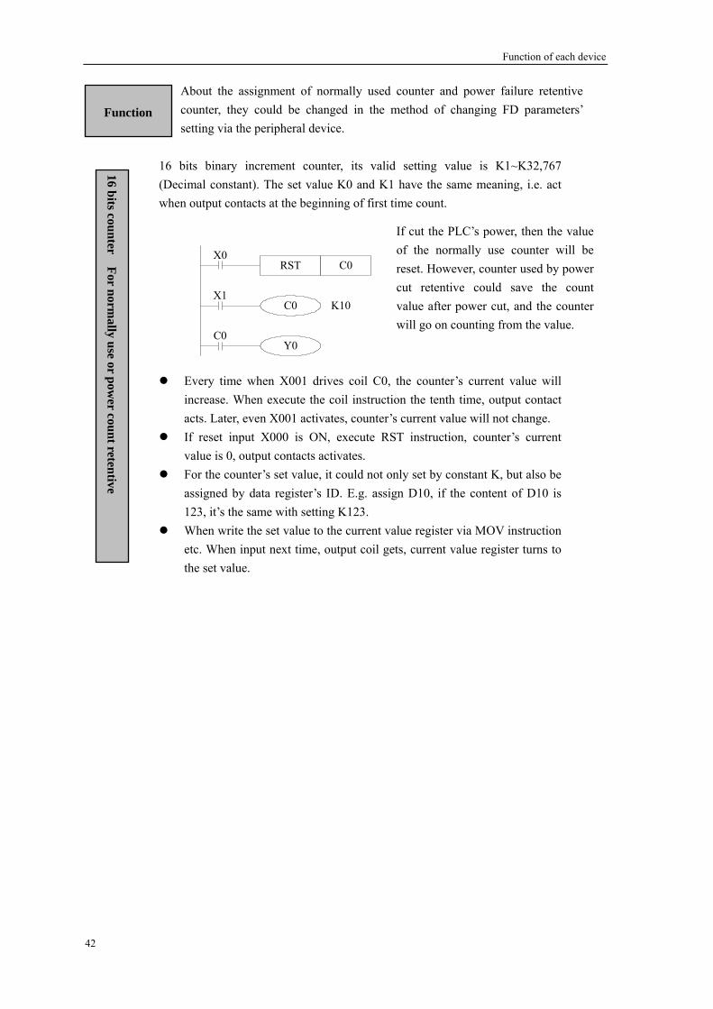
RST C0X0
C0 K10
Y0
X1
C0
About the assignment of normally used counter and power failure retentive counter, they could be changed in the method of changing FD parameters’ settin via the peripheral device. g
16 bits binary increment counter, its valid setting value is K1~K32,767 (Decimal constant). The set value K0 and K1 have the same meaning, i.e. act when output contacts at the beginning of first time count.
If cut the PLC’s power, then the value of the normally use counter will be reset. However, counter used by power cut retentive could save the count value after power cut, and the counter will go on counting from the value.
Every time when X001 drives coil C0, the counter’s current value will increase. When execute the coil instruction the tenth time, output contact acts. Later, even X001 activates, counter’s current value will not change.
If reset input X000 is ON, execute RST instruction, counter’s current value is 0, output contacts activates.
For the counter’s set value, it could not only set by constant K, but also be assigned by data register’s ID. E.g. assign D10, if the content of D10 is 123, it’s the same with setting K123.
When write the set value to the current value register via MOV instruction etc. When input next time, output coil gets, current value register turns to the set value.
Function
16 bits counter For normally use or pow
er count retentive
42
Function of each device
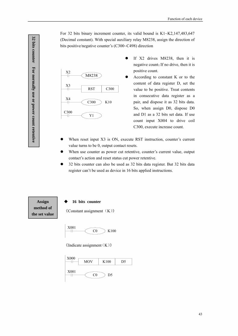
RST C300X3
C300 K10
Y1
X4
C300
M8238X2
C0X001
K100
For 32 bits binary increment counter, its valid bound is K1~K2,147,483,647 (Decimal constant). With special auxiliary relay M8238, assign the direction of bits positive/negative counter’s (C300~C498) direction
If X2 drives M8238, then it is negative count;If no drive, then it is positive count.
According to constant K or to the content of data register D, set the value to be positive. Treat contents in consecutive data register as a pair, and dispose it as 32 bits data. So, when assign D0, dispose D0 and D1 as a 32 bits set data. If use count input X004 to drive coil C300, execute increase count.
32 bits counter For normally use or pow
er count retentive When reset input X3 is ON, execute RST instruction, counter’s current value turns to be 0, output contact resets.
When use counter as power cut retentive, counter’s current value, output contact’s action and reset status cut power retentive.
32 bits counter can also be used as 32 bits data register. But 32 bits data register can’t be used as device in 16 bits applied instructions.
Assign method of
the set value
16 bits counter
《Constant assignment(K)》
《Indicate assignment(K)》
MOV K100 D5
C0 D5
X000
X001
43

Function of each device
C300X001
K43,100
DMOV K43100 D0
C300 D0( D1)
X000
X001
The count
value
The count mode of counters T0~T599 is 16 bits linear increment mode (0~K32767). When counter’s count value reaches the max value K32767, the counter will stop counting, the counter’s status will remain.
32 bits counter
《Constant assignment(K)》
《Indicate assignment(K)》
44

Function of each device
45
3-7. Some Points to Note
Action order of input/output relay and response delay》
《Not accept narrow input pulse signal》
Dual output(Dual coils)action》
《
《
Y3
Y4
Y3
X1
Y3
X2
PLC’s input ON/OFF time should be longer than its loop time. If consider input filter’s response delay 10ms, loop time is 10ms,then ON/OFF time needs 20 ms separately. So, up to 1,000/(20+20)=25Hz input pulse can’t be disposed. But, this condition could be improved when use PLC’s special function and applied instructions.
As shown in the left map, please consider the things of using the same coil Y003 at many positions: E.g. X001=ON,X002=OFF At first, X001 is ON, its image area is ON, output Y004 is also ON. But, as input X002 is OFF, the image area of Y003 is OFF. So, the actual output is : Y003=OFF, Y004= ON.
Input disposal Before PLC executing the program, read all the input terminal’s ON/OFF status of PLC to the image area. In the process of executing the program, even the input changed, the content
e. However, in the input disposal of next scan cycle, read out the change. Output disposal
Once finish executing all the instructions, transfer the ON/OFF status of output Y image area to the output lock memory area. This will be the actual output of the PLC. The contacts used for the PLC’s exterior output will act according to the device’s response delay time.
ormat in a batch, the drive time and operation cycle of input filter and output device will also appear response delay.
in the input image area will not chang
When use this input/output f
When executing dual output (use dual coil), the back side act in prior

In this chapter, we tell some basic instructions and their functions.
4. Basic Program Instructions
4-1.List of Basic Instructions
4-2.【LD】,【LDI】,【OUT】
4-3.【AND】,【ANI】
4-4.【OR】,【ORI】
4-5.【LDP】,【LDF】,【ANDP】,【ANDF】,【ORP】, 【ORF】
4-7.【ORB】
4-8.【ANB】
4-9.【MCS】,【MCR】
4-10.【ALT】
4-11.【PLS】, 【PLF】
4-12.【SET】, 【RST】
4-13.【OUT】, 【RST】 (Compare with counter’s soft unit)
4-14.【NOP】, 【END】
4-15.Note Items When Programming
4-6.Compare Instructions
46
Basic SFC Functions
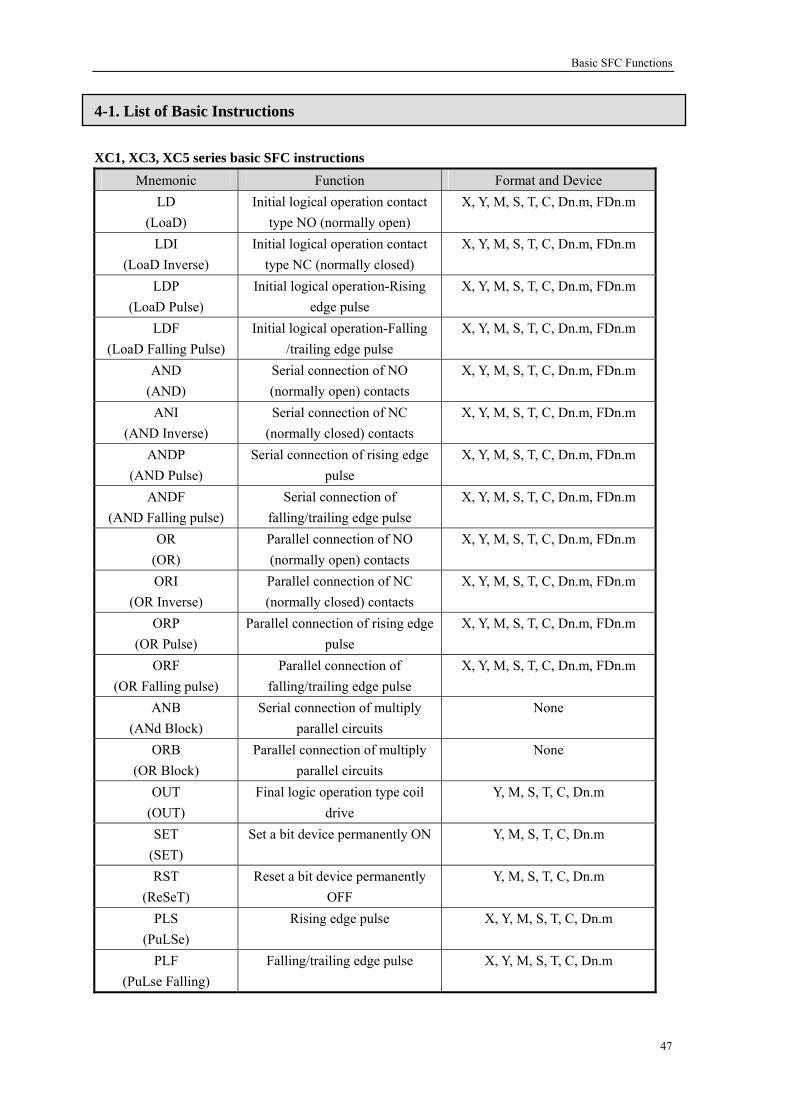
4-1. List of Basic Instructions XC1, XC3, XC5 series basic SFC instructions
Mnemonic Function Format and Device LD
(LoaD) Initial logical operation contact
type NO (normally open) X, Y, M, S, T, C, Dn.m, FDn.m
LDI (LoaD Inverse)
Initial logical operation contact type NC (normally closed)
X, Y, M, S, T, C, Dn.m, FDn.m
LDP (LoaD Pulse)
Initial logical operation-Rising edge pulse
X, Y, M, S, T, C, Dn.m, FDn.m
LDF (LoaD Falling Pulse)
Initial logical operation-Falling /trailing edge pulse
X, Y, M, S, T, C, Dn.m, FDn.m
AND (AND)
Serial connection of NO (normally open) contacts
X, Y, M, S, T, C, Dn.m, FDn.m
ANI (AND Inverse)
Serial connection of NC (normally closed) contacts
X, Y, M, S, T, C, Dn.m, FDn.m
ANDP (AND Pulse)
Serial connection of rising edge pulse
X, Y, M, S, T, C, Dn.m, FDn.m
ANDF (AND Falling pulse)
Serial connection of falling/trailing edge pulse
X, Y, M, S, T, C, Dn.m, FDn.m
OR (OR)
Parallel connection of NO (normally open) contacts
X, Y, M, S, T, C, Dn.m, FDn.m
ORI (OR Inverse)
Parallel connection of NC (normally closed) contacts
X, Y, M, S, T, C, Dn.m, FDn.m
ORP (OR Pulse)
Parallel connection of rising edge pulse
X, Y, M, S, T, C, Dn.m, FDn.m
ORF (OR Falling pulse)
Parallel connection of falling/trailing edge pulse
X, Y, M, S, T, C, Dn.m, FDn.m
ANB (ANd Block)
Serial connection of multiply parallel circuits
None
ORB (OR Block)
Parallel connection of multiply parallel circuits
None
OUT (OUT)
Final logic operation type coil drive
Y, M, S, T, C, Dn.m
SET (SET)
Set a bit device permanently ON Y, M, S, T, C, Dn.m
RST (ReSeT)
Reset a bit device permanently OFF
Y, M, S, T, C, Dn.m
PLS (PuLSe)
Rising edge pulse X, Y, M, S, T, C, Dn.m
PLF (PuLse Falling)
Falling/trailing edge pulse X, Y, M, S, T, C, Dn.m
47

Basic SFC Functions
MCS (New bus line start)
Connect the public serial contacts None
MCR (Bus line return)
Clear the public serial contacts None
ALT (Alternate state)
The status of the assigned device is inverted on every operation of
the instruction
X, Y, M, S, T, C, Dn.m
NOP (No Operation)
No operation or null step None
END (END)
Force the current program scan to end
None
48
Basic SFC Functions
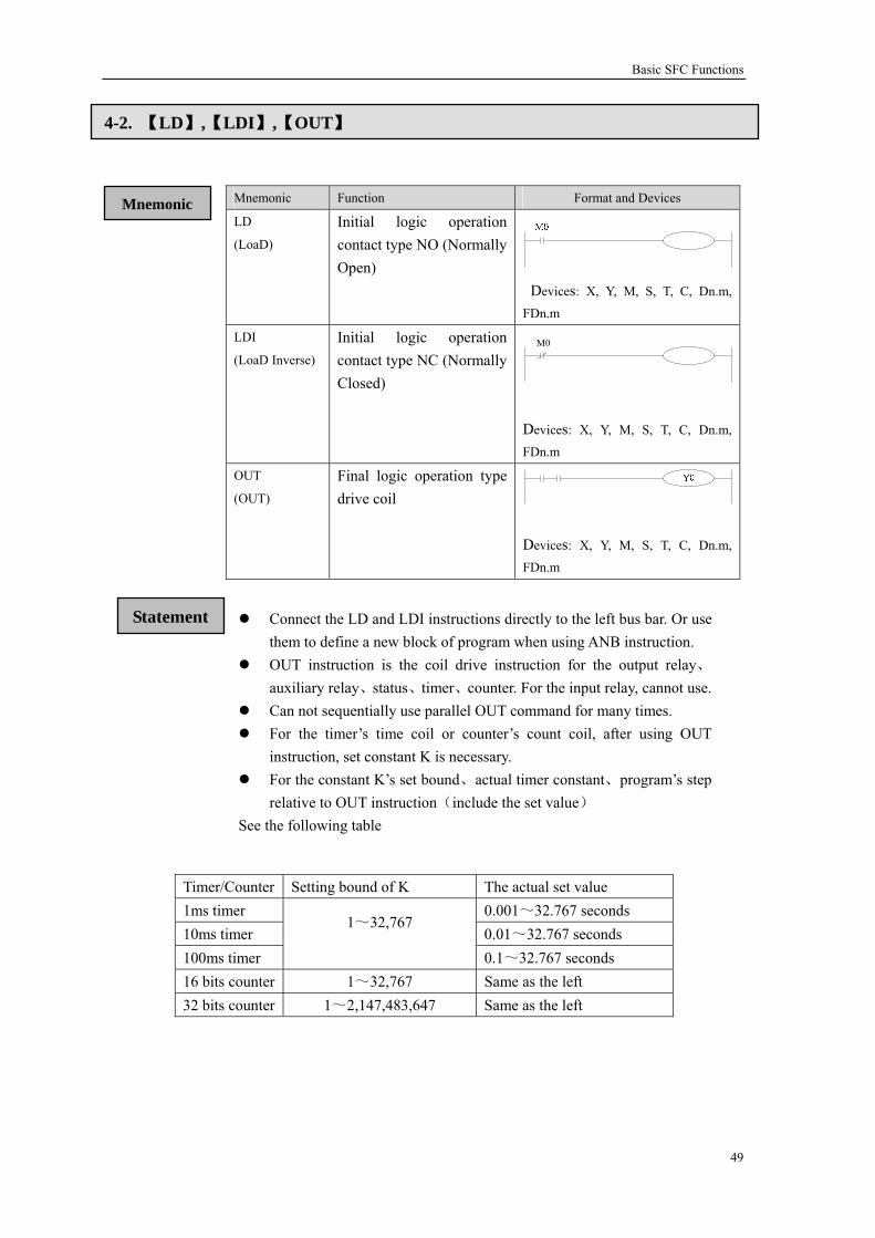
4-2. 【LD】,【LDI】,【OUT】
Mnemonic Function Format and Devices
LD
(LoaD)
Initial logic operation contact type NO (Normally Open)
Devices: X, Y, M, S, T, C, Dn.m,
FDn.m
LDI
(LoaD Inverse)
Initial logic operation contact type NC (Normally Closed)
M0
Devices: X, Y, M, S, T, C, Dn.m,
Dn.m F
OUT
(OUT)
Final logic operation type drive coil
Devices: X, Y, M, S, T, C, Dn.m,
FDn.m
r Setting bound of K Timer/Counte The actual set value 1ms timer 0.001~32.767 seconds 10ms timer 0.01~32.767 seconds 100ms timer 0.1~32.767 seconds
1~32,767
16 bits counter 1~32,767 Same as the left 32 bits cou ter 1~2,147,483,647 Same as the left n
Connect the LD and LDI instructions directly to the left bus bar. Or use them to define a new block of program when using ANB instruction.
OUT instruction is the coil drive instruction for the output relay、auxiliary relay、status、timer、counter. For the input relay, cannot use.
Can not sequentially use parallel OUT command for many times. For the timer’s time coil or counter’s count coil, after using OUT
instruction, set constant K is necessary. For the constant K’s set bound、actual timer constant、program’s step
relative to OUT instruction(include the set value)
Mnemonic
Statement
See the following table
49

Basic SFC Functions
Y100
M1203
T 0
X0
Y 1
X1
T0K19
-3. 【AND】,【ANI】
Program LD X0 OUT Y100 LDI X1
3 OUT T0 SP K19 LD T0
OUT M120
OUT Y1
4
Mnemonic Function Format and Devices
AND (AND)
Serial connection of NO (Normally Open) contacts
M0
Devices: X, Y, M, S, T, C, Dn.m, FDn.m ANI (ANd Inverse)
Serial connection of NC (Normally Closed) contacts
M0
Devices: X, Y, M, S, T, C, Dn.m, FDn.m
50
Use the AND and ANI instructions for serial connection of contacts. As many contacts as required can be connected in series. They can be used for many times.
The output processing to a coil, through writing the initial OUT instruction is called a “follow-on” output (For an example see the program below: OUT M2 and OUT Y003). Follow-on outputs are
e output order is correct. There’s contacts’ No. and follow-on outputs’
permitted repeatedly as long as thno limit for the serial connected number.
Description
Program LD X2 AND M1 OUT Y2 LD Y2 ANI X3
Y2
M2
Y3
X2 M1
X3Y2
T1
Mnemonic

Basic SFC Functions
4-4. 【OR】,【ORI】
51
Mnemonic Function Format and Devices
OR (OR)
Parallel connection of NO (Normally Open) contacts
Devices: X, Y, M, S, T, C, Dn.m, FDn.m ORI (OR Inverse)
Parallel connection of NC (Normally Closed) contacts
Devices: X, Y, M, S, T, C, Dn.m, FDn.m
Program
Mnemonic and
Function
Description Use the OR and ORI instructions for parallel connection of contacts.
To connect a block that contains more than one contact connected in series to another circuit block in parallel, use an ORB instruction.
OR and ORI start from the instruction’s step, parallel connect with the LD and LDI instruction’s step said before. There is no limit for the parallel connect times.
LD X5 OR X6 OR M11 OUT Y6 LDI Y6 AND M4 OR M12 ANI X7 OR M13
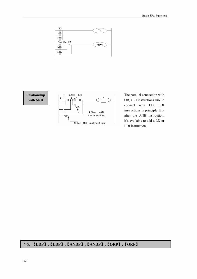
Basic SFC Functions
The parallel connection with OR, ORI instructions should connect with LD, LDI instructions in principle. But after the ANB instruction, it’s available to add a LD or LDI instruction.
Y6
M100
X5
X6
M11
Y6 M4 X7
M12
M13
Relationship with ANB
4-5. 【LDP】,【L 【AND P ,【ORF】
DF】, P】,【ANDF】,【OR 】
52
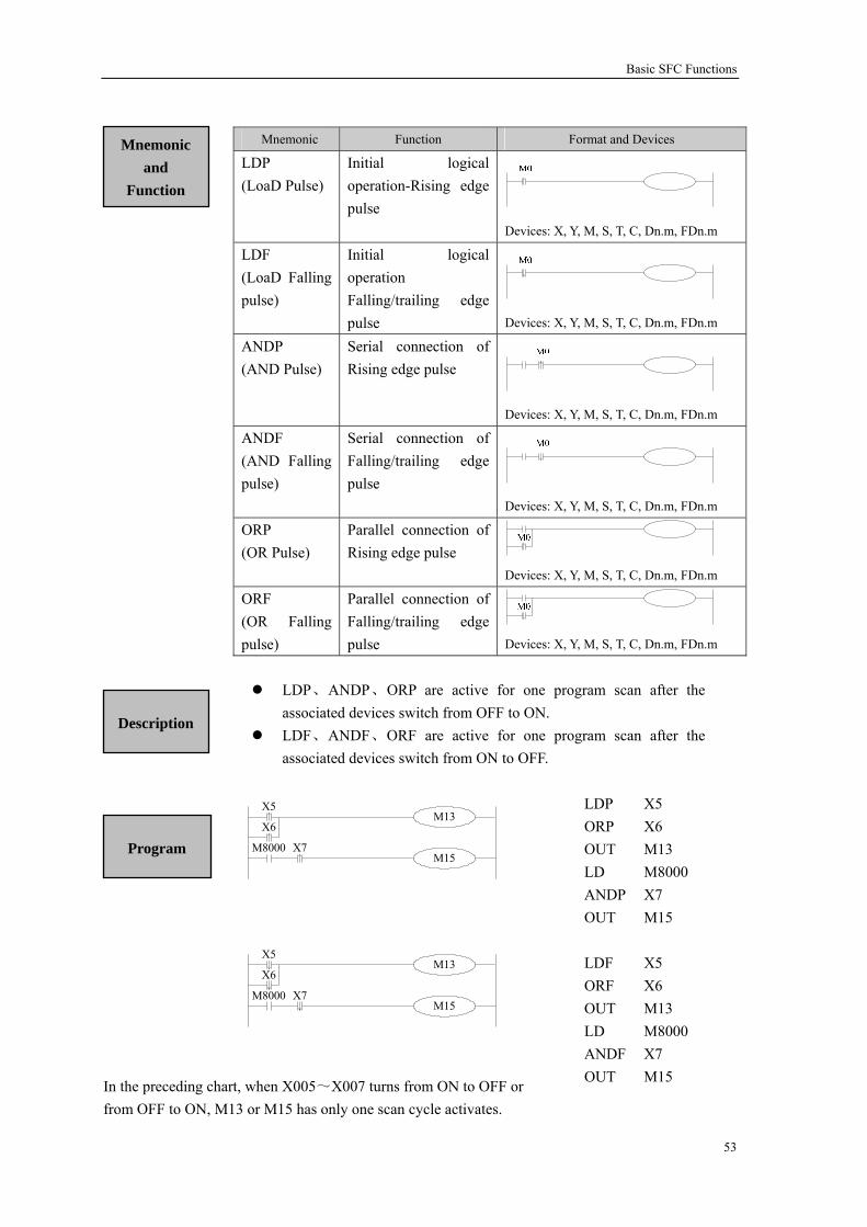
Basic SFC Functions
Mnemonic Function Format and Devices
LDP (LoaD Pulse)
gical operation-Rising edge Initial lo
pulse
Devices: X, Y, M, S, T, C, Dn.m, FDn.m LDF (LoaD Falling pulse)
Initial logical operation Falling/trailing edge pulse
Devices: X, Y, M, S, T, C, Dn.m, FDn.m ANDP (AND Pulse)
Serial connection of Rising edge pulse
Devices: X, Y, M, S, T, C, Dn.m, FDn.m ANDF Serial connection of (AND Falling pulse)
Falling/trailing edge pulse
Devices: X, Y, M, S, T, C, Dn.m, FDn.m ORP (OR Pulse)
Parallel connection of Rising edge pulse
Devices: X, Y, M, S, T, C, Dn.m, FDn.m ORF (OR Falling pulse)
Parallel connection of Falling/trailing edge pulse
Devices: X, Y, M, S, T, C, Dn.m, FDn.m
In the preceding chart, when X005~X007 turns from ON t OFF or
om OFF to ON, M13 or M15 has only one scan cycle activates.
Mnemonic and
Function
Description
LDP、ANDP、ORP are active for one program scan after the associated devices switch from OFF to ON.
e program scan after the OFF.
LDF、ANDF、ORF are active for onassociated devices switch from ON to
M13
M15
X5
X6
M8000 X7
M13
M15
X5
o fr
X6
M8000 X7
LDP X5 ORP X6 OUT M13 LD M8000 ANDP X7 OUT M15
LDF X5 ORF X6 OUT M13 LD M8000 ANDF X7 OUT M15
Program
53
Basic SFC Functions
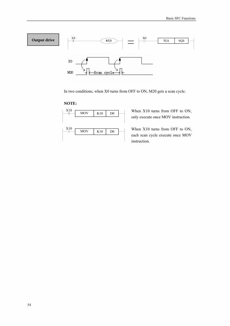
In two conditions, when X0 turns from OFF to ON, M20 gets a scan cycle. NOTE:
X10MOV K10 D0
X10
MOV K10 D0
Output drive
When X10 turns from OFF to ON, only execute once MOV instruction. When X10 turns from OFF to ON, each scan cycle execute once MOV instruction.
54

Basic SFC Functions
4-7. 【ORB】
Mnemonic Function Format and Devices
ORB (OR Block)
Parallel connection of multiply parallel circuits
Devices: none
Program
Description To declare the starting point of the circuit (usually serial circuit blocks)
to the preceding circuit in parallel. Serial circuit blocks are those in which more than one contacts in series or the ANB instruction is used.
An ORB instruction is an independent instruction and is not associated with any device number.
There are no limitations to the number of parallel circuits when using an ORB instruction in the sequential processing configuration.
When using ORB instructions in a batch, use no more than 8 LD and LDI instructions in the definition of the program blocks (to be connected parallel).
Recommended sequencial programming method: LD X0 AND X1 LD X2 AND X3 ORB LDI X4 AND X5 ORB
Non-preferred batch programming method: LD X0 AND X1 LD X2 AND X3 LDI X4 AND X5 ORB
Mnemonic and
Function
55

Basic SFC Functions
4-8. 【ANB】
Mnemonic Function Format and Devices
ANB (ANd Block)
Serial connection of multiply parallel circuits
Devices: none
Start of a branch
End of a parallel circuit block Serial connect with the preceding circuit
Start of a branch End of a parallel circuit block
Mnemonic
To declare the starting point of the circuit block, use a LD or LDI instruction. After completing the parallel circuit block, connect it to the preceding block in series using the ANB instruction.
It is possible to use as many ANB instructions as necessary to connect a number of parallel circuit blocks to the preceding block in series. When using ANB instructions in a batch, use no more than 8 LD and LDI instructions in the definition of the program blocks (to be connected in parallel)
Description
Program
LD X0 OR X1
AND X3 4
AND
OR X6 ANB OR X7 OUT Y20
LD X2
LDI X X5 ORB
56
Basic SFC Functions
4-9. 【MCS】,【MCR】
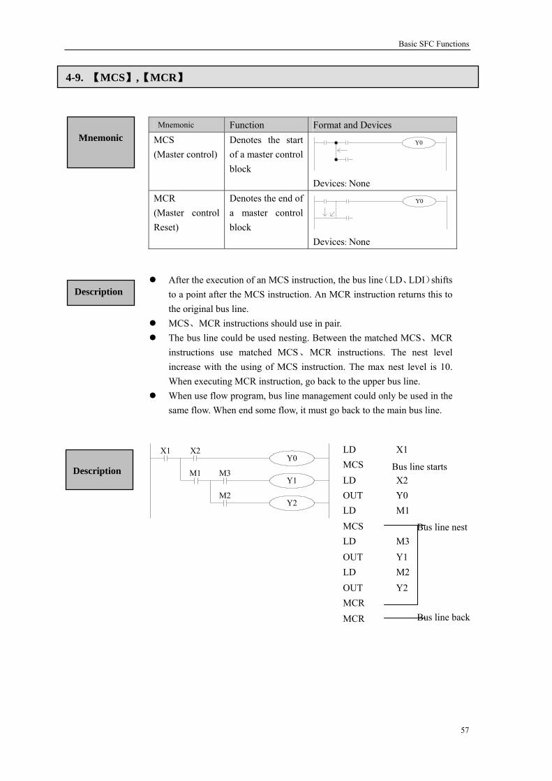
Mnemonic Function Format and Devices
MCS (Master control)
Denotes the start of a master control block
Y0
Devices: None
MCR (Master control Reset)
control block
Denotes the end of a master
Y0
Devices: None
X1 X2
M2
M3M1
Y0
Y1
Y2
Description
Description
Mnemonic
After the execution of an MCS instruction, the bus line(LD、LDI)shifts to a point after the MCS instruction. An MCR instruction returns this to the original bus line.
MCS、MCR instructions should use in pair. The bus line could be used nesting. Between the matched MCS、MCR
instructions use matched MCS、MCR instructions. The nest level increase with the using of MCS instruction. The max nest level is 10. When executing MCR instruction, go back to the upper bus line.
When use flow program, bus line management could only be used in the same flow. When end some flow, it must go back to the main bus line.
LD X1 MCS
LD X2 OUT Y0 LD M1 MCSLD M3 OUT Y1 LD M2 OUT Y2
MCR
Bus line starts
MCR
Bus line nest
Bus line back
57

Basic SFC Functions
4-10. 【ALT】
Mnemonic Function Format and Devices
ALT (Alternate status)
The status of the assigned devices inverted on every operation of the instruction
M0ALT
Devices: Y, M, S, T, C, Dn.m
M0ALT
M0Y0
M100
Y1M0
Description
Program
Mnemonic and
Function
The status of the destination device is alternated on every operation of the ALT instruction.
LDP M100 ALT M0 LD M0 OUT Y0 LDI M0 OUT Y1
58

Basic SFC Functions
4-11. 【PLS】,【PLF】
Mnemonic Function Format and Devices
PLS (PuLSe)
Rising edge pulse
Devices: Y, M, S, T, C, Dn.m
PLF (PuLse Falling)
Falling/trailing edge pulse
Devices: Y, M, S, T, C, Dn.m
X0
PLS M0
M0SET Y0
X1PLF M1
M1RST Y0
Mnemonic and
Function
Description When a PLS instruction is executed, object devices Y and M operate
for one operation cycle after the drive in ut signal has turned ON. When a PLF instruction is executed, object devices Y and M operate
for one operation cycle after the drive input signal has turned OFF.
p
Program
LD X0 PLS M0 LD M0 SE---------------------- LD X1
LD M1
T Y0
PLF M1
RST Y0
59

Basic SFC Functions
4-12. 【SET】,【RST】
Mnemonic Function Format and Devices
SET (SET)
Set a bit device permanently ON
Devices: Y, M, S, T, C, Dn.m RST (ReSeT)
Reset a bit devicepermanently OFF
Devices: Y, M, S, T, C, Dn.m
Mnemonic and
Function
Description Turning ON X010 causes Y000 to turn ON. Y000 remains ON even
after X010 turns OFF. Turning ON X 1 causes Y000 to turn OFF. Y000 remains OFF even after X011 turns OFF. It’s the same with M、
SET and RST instructions can be used for the same device as many times as necessary. However, the last instruction activated determines
nt status. nd defi he
nds available. sides, ssible to use RST instruct n to reset the current
contents
01
S.
the curreAfter assign opera
the start definition ID and e in one bound at the same time is
it’s also po
nition ID, operate t
Be ioof timer, counter and contacts.
X10SET Y0
X11RST Y0
X12SET M50
X13RST M50
X14SET S0
X15RST S0
X10T250
K10
X17RST T250
Program
LD X10 SET Y0 LD X11 RST Y0 LD X12 SET M50 LD X13 RST M50 LD X14 SET S0 LD X15 RST S0 LD X10 OUT T250 SP K10 LD X17 RST T250
60

Basic SFC Functions
4-13. 【OUT】,【RST】for the counters
Mnemonic Function Format and Devices
OUT (OUT)
Final logic operation type coil drive
K or D RST (ReSeT)
Reset a bit devicepermanently OFF
Counter used for ut retentive. Even when power is cut, hold the current value and output contact’s action status and reset status.
power c
Mnemonic and
Function
Programming
C0 carries on increase count for the OFF→ON of X011. When reach the
value K10, output contact C0 activates. Afterwards, even X011 turns
m OFF to ON, counter’s current value will not change, output contact keep on activating. To clear this, let X010 be the activate status and reset the output contact. It’s necessary to assign constant K or indirect data register’s ID behind OUT instruction.
set
fro
Programming of high speed
counter
In the preceding example, when M0 is ON, carry on positive count with OFF→ON of X0.
Counter’s current value increase, when reach the set value (K or D), the output contact is reset.
When M1 is ON, counter’s C600 output contact is reset, counter’s current value turns to be 0.
61

Basic SFC Functions
4-14. 【NOP】,【END】
Mnemonic Function Format and Devices: None
NOP No operation (No Operation)
or null step Devices: None
END Force t(END)
hecurrent program scan
to end
Devices: None
Description When clear the whole program, all the instructions become NOP. If add
NOP instructions between the common instructions, they have no effect and PLC will keep on working. If add NOP instructions in the program,
n modify or add programs, the step vary will be decreased. But
with NOP instructions, then the
PLC repeatedly carry on input disposal, program executing and output disposal. If write END instruction at the end of the program, then the instructions behind END instruction won’t be executed. If there’s no END instruction in the
When debug, insert END in each program segment to check out each program’s action. Then, after confirm the correction of preceding block’s action, delete END instruction. Besides, the first execution of RUN begins with END instruction.
then whethe program should have rest quantity.
If replace the program’s instructions
When executing END instruction, refresh monitor timer. (Check if scan cycle is a long timer. )
program, the PLC executes the end step and then repeat executing the program from step 0.
OUT→NOP
AND→NOP ANI→NOP
Contacts short circuit OR→NOP ORI→NOP
Open circuit
62

Basic SFC Functions
63
4-15. Items To Note When Programming
, Contacts’ structure and step number Even in the sequencial control circuit with the same action, it’s also available to simple the
and save program’s steps according to the contacts’ structure. General program principle is: he circuit with many serial contacts on the top;b)write the circuit with many parallel contacts
left.
, Program’s executing sequence Handle the sequencial control program by【From top to bottom】and【From left to right】
ncial control instructions also encode following this flow.
, Dual output dual coil’s activation and the solution If carry on coil’s dual output (dual coil) in the sequencial control program, then the backward
action is prior. Dual output (dual coil) doesn’t go against the input rule at the program side. But as the preceding
action is very complicate, please modify the program as in the following example.
1
programa)write tin the 2
Seque 3
Y0
Y0
X0 X2
X3 X4
Y0X0 X2
X3 X4
M0
M1
X0 X2
X3 X4
Y0M0
M1
There are other methods. E.g. jump instructions or step ladder. However, when use step ladder, if the main program’s output coil is programmed, then the disposal method is the same with dual coil, please note this.
Applied Instructions
In this chapter, we describe applied instruction’s function of XC series PLC.
5. Applied Instructions
5-1.Table of App ructions lied Inst
5-2.Reading Meth Applied Instructions od of
5-3.Flow Instructions
5-4.Contactors Co Instructions mpare
5-5.Move and Co nstructions mpare I
5-6.Arithmetic an on Instructions d Logic Operati
5-7.Loop and Shift tions Instruc
5-8.Data Convert
5-9.Floating Operation
5-10.Clock Operation
64
Applied Instructions
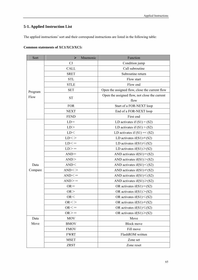
5-1. Applied Instruction List The applied instructions’ sort a r correspond instructions are listed i ing table: Common statements of XC1/ C5:
nd thei n the follow
XC3/X
Sort Mnemonic Function CJ Co p ndition jum
CALL C e all subroutinSRET Subro turn utine reSTL Flow start
STLE Flow end SET Open the assi urrent flow gned flow, close the c
ST Open the assign ose the current ed flow, not cl
flow FOR Start of a FOR-NEXT loop
NEXT End of a FOR-NEXT loop
Program Flow
FEND First end LD= LD activates if (S1) = (S2) LD> LD activates if (S1) > (S2) LD< LD activates if (S1) =< (S2)
LD<> LD activates if(S1)≠(S2) LD<= LD activates if(S1)≤(S2) LD>= LD activates if(S1)≥(S2) AND= AND activates if(S1)=(S2) AND> AND activates if(S1)>(S2) AND< AND activates if(S1)<(S2)
AND<> AND activates if(S1)≠(S2) AND<= AND activates if(S1)≤(S2) AND>= AND activates if(S1)≥(S2)
OR= OR activates if(S1)=(S2) OR> OR activates if(S1)>(S2) OR< OR activates if(S1)<(S2)
OR<> OR activates if(S1)≠(S2) OR<= OR activates if(S1)≤(S2)
Data Compare
OR>= OR activates if(S1)≥(S2) MOV Move
BMOV Block move FMOV Fill move FWRT FlashROM written MSET Zone set
Data Move
ZRST Zone reset
65

Applied Instructions
SWAP The high and low byte of the destinated devices
are exchanged XCH ange ExchADD tion AddiSUB Subtraction MUL iplication MultDIV Division INC Increment DEC Decrement
MEAN Mean WAND Word And WOR Word OR
WXOR Word exclusive OR CML Compliment
Data Operation
NEG Negative
66

Applied Instructions
Common statements of XC3/XC5
SHL Arithmetic Shift Left SHR Arithmetic Shift Right LSL Logic shift left LSR Logic shift right ROL Rotation shift left ROR Rotation shift right SFTL Bit shift left SFTR Bit shift right WSFL Word shift left
Data Shift
WSFR Word shift right WTD Single word integer converts to double word integer FLT 32 bits integer converts to float point
FLTD 64 bits integer converts to float point INT Float point converts to binary BIN BCD converts to binary BCD Binary converts to BCD ASC Hex. converts to ASCII HEX ASCII converts to Hex.
DECO Coding ENCO High bit coding
Data Convert
ENCOL Low bit coding ECMP Float compare EZCP Float Zone compare EADD Float Add ESUB Float Subtract EMUL Float Multiplication EDIV Float division ESQR Float Square Root SIN Sine COS Cosine
Float Point eration
TAN Tangent
Op
TCMP Time Compare TZCP Time Zone Compare TADD Time Add TSUB Time Subtract TRD Read RTC data
Clock Operation
TWR Set RTC data
67
Applied Instructions
5-2. Reading Method of Applied Instructions nderstanding method of instruction understanding this manual, the applied instructions are described in the following manner.
UIn
Note:
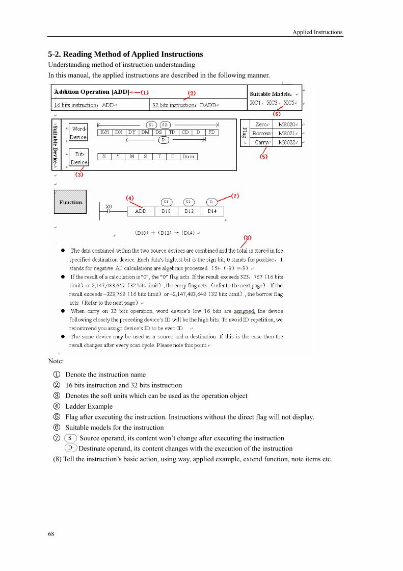
① Denote the instruction name ② 16 bits instruction and 32 bits instruction ③ Denotes the soft units which can be used as the operation object ④ Ladder Example ⑤ Flag after executing the instruction. Instructions without the direct flag will not display. ⑥ Suitable models for the instruction ⑦ Source operand, its content won’t change after executing the instruction
Destinate operand, its content changes with the execution of the instruction (8) Tell the instruction’s basic action, using way, applied example, extend function, note items etc.
D· S·
68

Applied Instructions
The assignment of the data
The related The data register of XC series PLC is a single word (16 bit) data register, single word data only engross one data register which is assi singlobject instruction. The disposal bound is: Dec. –3 327,67, x. 0000~FFFF.
gned by e word 27,68~ He
Instruction D(NUM) Object data
Instruction D(NUM) Object data Object data
description
The denote way of 32 bits instruction If an instruction can not only be 16 bits but al , then t denote m r 32 bits instruction is to add a “D” before 16 bits instruction. E.g:ADD D0 D2 D4 denotes two 16 bits data adds;
DADD D10 D12 D14 denotes two 32 bits data adds
Single word object instruction D(NUM)
Double word(32 bit)engrosses two data register, it’s composed by tw cutive dat registers, the first one is assigned by double word object instruc he dispo bound is: Dec. -214,748,364,8~214,748,364,7, Hex. 00000000~FFFFFFFF.
o consetion. T
ase
Double word object instruction D(NUM)D(NUM+1)
so be 32 bits he ethod fo
69

Applied Instructions
Instructions list of 16 bits and correspond 32 bits:
16 bits 32 bits
WTD - FLT DFLT INT DINT BIN DBIN BCD DBCD ASC - HEX -
DECO - ENCO -
Da
ENCOL -
ta convert
- ECMP - EZCP - EADD - ESUB - EMUL - EDIV - ESQR - SIN - COS
Float opera
TAN
tion
TCMP - TZCP - TADD - TSUB - TRD -
Clock operation
TWR -
16 bits 32 bits CJ -
CALL - SRET - STL -
S LE T SET ST
FOR - NEXT -
Program Flow
FEND - MOV DMOV
BMOV FMOV - FWRT DFWRT ZRST - SWAP -
Data Move
XCH DXCH
ADD DADD SUB DSUB MUL DMUL DIV DDIV INC DINC DEC DDEC
MEAN DMEAN WAND DWAND WOR DWOR
WXOR DWXOR CML DCML
Data operation
NEG DNEG SHL DSHL SHR DSHR LSL DLSL LSR DLSR ROL DROL ROR DROR SFTL DSFTL SFTR DSFTR WSFL DWSFL
Data Shift
WSFR DWSFR
70

Applied Instructions
71
5-3. Program Flow Instructions
Mnemonic Instruction’s name CJ Condition Jump
CALL Call subroutine SRET Subroutine return STL Flow start
STLE Flow end SET jump) Open the assigned flow, close the current flow (flowST Open the assigned flow, not close the current flow (Open the
new flow) FOR Start of a FOR-NEXT loop
NEXT End of a FOR-NEXT loop FEND First End

Applied Instructions
As the instructions of executing list, with CJ instructions, the operate cycle and dual coil can be greatly shorten. In the following chart, if X000“ON”, then jump from step 1 to the end step of flag P6. When X000“OFF”, do not execute jump instructions.
CJ
Y0
X0
X1
X3
X4
X0
RST
T246 K1000
MOV
CJ
X2
X5
X6
P6
T246
K3 D0
P7
T246RST
Y0
P6
P7
See the upward graph, Y000 turns to be dual coil and output. But when X000=OFF, X001 activates. When X000=ON, X005 activates.
CJ can not jump from one STL to another STL. If program timer T0~T640 and high speed counter C600~C640 jump
after driving, go on working, output point also activate.
Condition Jump [CJ]
16 bits instruction:CJ 32 bits instruction:-
Suitable Models: XC1、XC3、XC5
Pointer: P
Soft Unit’s Bound: P0~P9999
Suitable Device
Function
and Action
72
Applied Instructions
CALLX0
FEND
SRET
END
P10
P10
Call subroutine [CALL] and Subroutine return [SRET]
16 bits instruction:CALL、SRET 32 bits instruction:-
Suitable Models: XC1、XC3、XC5
Function
If X000“ON”, carry on Jump instruction and jump to step of flag P10. Here, after executing the subroutine, return to the original step via executing SRET instruction. After the following FEND instruction, program with the flag.
In the subroutine, 9 levels Call instruction is allowed, so to the all, 10 levels nesting is available.
Main program
Subroutine
Pointer: P
Soft Unit’s Bound: P0~P9999
Suitable Device
73

Applied Instructions
SET S0
STL S0
SET S1
ST S2
STL S1
STLE
STLE
STL S2
STLE
STL and STLE should be used in pairs. STL means start of a flow, STLE means end of a flow.
After executing of SET Sxxx instruction, the flow assigned by these instructions is ON. After executing RST Sxxx instruction, the assigned flow is OFF. In flow S0, SET S1 close the current flow S0, open flow S1. In flow S0, ST S2 open the flow S2, but don’t close flow S0. When flow turns from ON to be OFF, OFF or reset OUT、PLS、PLF、not accumulate timer
etc. which belongs to the flow. ST instruction is usually used when a program needs to run more flows at the same time. In a main program, usually use ST instruction to open a flow.
Flow [SET]、[ST] 、[STL]、 [STLE]
16 bits instruction:SET、ST、STL、STLE 32 bits instruction:-
Suitable Models: XC1、XC3、XC5
Pointer: S
Soft Unit’s Bound: S0~S
Suitable Device
Function
74
Applied Instructions
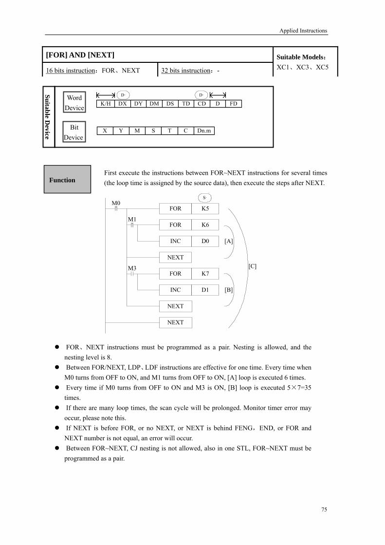
First execute the instructions between FOR~NEXT instructions for several times (the loop time is assigned by the source data), then execute the steps after NEXT.
FOR K6
INC D0
NEXT
FOR K7
INC D1
NEXT
NEXT
FOR K5M0
M3
M1
[A]
[B]
[C]
S·
FOR、NEXT instructions must be programmed as a pair. Nesting is allowed, and the nesting level is 8.
Between FOR/NEXT, LDP、LDF instructions are effective for one time. Every time when M0 turns from OFF to ON, and M1 turns from OFF to ON, [A] loop is executed 6 times.
Every time if M0 turns from OFF to ON and M3 is ON, [B] loop is executed 5×7=35 times.
If there are many loop times, the scan cycle will be prolonged. Monitor timer error may occur, please note this.
If NEXT is before FOR, or no NEXT, or NEXT is behind FENG,END, or FOR and NEXT number is not equal, an error will occur.
Between FOR~NEXT, CJ nesting is not allowed, also in one STL, FOR~NEXT must be programmed as a pair.
[FOR] AND [NEXT]
16 bits instruction:FOR、NEXT 32 bits instruction:-
Suitable Models: XC1、XC3、XC5
Suitable Device
Word D FDDMDX DY DS TD CDK/H
Device
Bit Device
X Y M S T C Dn.m
D· D·
Function
75

Applied Instructions
A of the pr es the FE output p t on ex
[FEND] AND [END]
1
n FEND instruction indicates the first end of a main program and the start ogram area to be used for subroutines. Under normal operating circumstancND instruction performs a similar action to the END instruction, i.e.
rocessing, input processing and watchdog timer refresh are all carried ouecution.
6 bits instruction:FEND、END 32 bits instruction:-
Suitable Models: XC1、XC3、XC5
None
Suitable Device
Function
If program the tag of CALL instruction behind FEND instruction, there must be SRET
instruction. If the interrupt pointer program behind FEND instruction, there must be SRET instruction.
After executing CALL instruction and before executing SRET instruction, if execute FEND instruction; or execute FEND instruction after executing FOR instruction and before executing NEXT, then an error will occur.
In the condition of using many FEND instruction, please compile routine or subroutine between the last FEND instruction and END instruction.
76

Applied Instructions
5-4. Contactor’s Compare Instructions
Mnemonic Function
LD= Initial comparison contact. Active when the comparison (S1)=(S2) is true. LD> Initial comparison contact. Active when the comparison (S1)> (S2) is true LD< Initial comparison contact. Active when the comparison (S1)< (S2) is true
LD<> Initial comparison contact. Active when the comparison (S1)≠(S2) is true LD<= Initial comparison contact. Active when the comparison (S1)≤(S2) is true LD>= Initial comparison contact. Active when the comparison (S1)≥(S2) is true AND= Seri ison contact. Active when parison (S1)=(S2)is eal compar the com tru . AND> Serial com act. Active when mparison (S1)> (S2) is trueparison cont the co . AND< Serial com act. Active when comparison (S1)< (S2) is trueparison cont the .
AND Serial compari n the comp (S2) is true. <> son contact. Active whe arison (S1)≠AND<= Serial comparison contact. Active when the comparison (S1)≤(S2) is true. AND Serial compari n the comp (S2) is true. >= son contact. Active whe arison (S1)≥
OR= Parallel comparison contact. Active when the comparison (S1)=(S2) is true. O Parallel compar Active when the com > (S2) is true. R> ison contact. parison (S1)OR< Parallel comparison contact. Active when the comparison (S1)< (S2) is true.
OR Parallel compar Active when the com ≠(S2) is true. <> ison contact. parison (S1)OR<= Parallel comparison contact. Active when the comparison (S1)≤(S2) is true. OR Parallel comparison . Active when the com ≥(S2) is true. >= contact parison (S1)
Mnemonic & Function
77

Applied Instructions
The value of S1 and S2 are tested according to the comparison of the instruction. If the comparison is
ue then the LD contact is active. If the comparison is false then the LD contact is not active.
its 32
bits
Active condition
Inactive condition
tr16 b
LD
DLD= (S1)=(S2) (S1)≠(S2) =
LD>
DLD> (S1)>(S2) (S1)≤(S2)
L<
DLD< (S1)<(S2) (S1)≥(S2) D
LD
>
DLD<> (S1)≠(S2) (S1)=(S2) <
LD<
DLD<= (S1)≤(S2) (S1)>(S2)
=
L DLD>= (S1)≥(S2) (S1)<(S2) D>
=
LD> D200 K-30 SET Y1
DLD> K68899 C300 M50
X0
M4
S1· S2·
LD= K100 C0 Y0X0
Instruction & Function
Program
nitial Comparison LD I
16 bits instruction:Refer Below 32 bits instruction:Refer Below
Suitable Models: XC1、XC3、XC5
Word Device
Bit Device
X Y M S T C Dn.m
D FDDMDX DY DSS1· S2·
TD CDK/H
78

Applied Instructions
The value of S1 and S2 are tested according to the comparison of the instruction. If the comparison is true then the LD contact is active. If the comparison is false then the LD contact is not active.
16 bits
32 bits
Active condition
Inactive condition
AND=
DAND= (S1)=(S2) (S1)≠(S2)
AND>
DAND> (S1)>(S2) (S1)≤(S2)
AND<
DAND< (S1)<(S2) (S1)≥(S2)
AND<>
DAND<> (S1)≠(S2) (S1)=(S2)
AND<=
DAND<= (S1)≤(S2) (S1)>(S2)
AND>=
DAND>= (S1)≥(S2) (S1)<(S2)
When the source data’s highest bit (16 bits:b15,32 bits:b31) is 1,use the data as a negative.
The comparison of 32 bits counter (C300~) must use 32 bits instruction. If assigned as 16 bits instruction, it will lead the program error or operation error.
Note Items
Instruction & Function
Program
Serial Refer Below AND
16 bits instruction:Refer Below 32 bits instruction:Refer Below
Suitable Models: XC1、XC3、XC5
Word Device
Bit Device
X Y M S T C Dn.m
D FDDMDX DY DSS1· S2·
TD CDK/H
79

Applied Instructions
AND= K100 C0 Y0
AND> D0K-30 SET Y1
DAND> K68899 D10 M50
X1
M4
X0
X2
S1· S2·
Note Items When the source data’s highest bit (16 bits:b15,32 bits:b31) is 1,
use the data as a negative. The comparison of 32 bits counter (C300~) must use 32 bits instruction.
If assigned as 16 bits instruction, it will lead the program error or operation error.
80

Applied Instructions
T e of S1 and S2 cording to the instruction. If the comparison is true then the AND c active. If the c n the AND contact is not active.
6 bits 32 bits Active condition Inactive condition
he valu are tested acontact is omparison is false the
1AND= DAND= (S1)=(S2) (S1)≠(S2) AND> DAND> (S1)>(S2) (S1)≤(S2) AND< DAND< (S1)<(S2) (S1)≥(S2) AND<> DAND<> (S1)≠(S2) (S1)=(S2) AND<= DAND<= (S1)≤(S2) (S1)>(S2) AND>= DAND>= (S1)≥(S2) (S1)<(S2)
OR= K100 C0
Y0
DOR> K68899D10
M50M4
X0
X2
S1· S2·
Instruction & Function
Program
When the source data’s highest bit (16 bits:b15,32 bits:b31) is 1,use the data as a negative.
The comparison of 32 bits counter (C300~) must be 32 bits instruction. If assigned as a 16 bits instruction, it will lead the program error or operation error.
Note Items
ision OR Parallel Compar
16 bits instruction:Refer Below 32 bits instruction:Refer Below
Suitable Models: XC1、XC3、XC5
Word Device
Bit vice
D FDDMDX DY DSS1· S2·
TD CDK/H
X M S T C Dn.mYDe
81

Applied Instructions
5-5. Data Move
Mnemonic Function MOV Move BMOV Block Move FMOV Fill Move FWRT Written of FlashROM MSET Zone Set ZRST Zone Reset SWA Float To Scientific PXCH Exchange
82

Applied Instructions
MOV K10 D10X0
S· D·
value of timer, counter》
《Read out the current
MOV T0 D20X1
Indirect assign the set value of timer, counter》
《
MOV K10 D20X2
M0T20 D20
《Move of 32 bits data》
DMOV D0 D10
DMOV C235 D20
Function & Action
Move data from one storage area to a new one.
(K10)(D10)
D20=K10
(T0 current value)→(D20)
It’s the same with the counter.
(D1,D0)→(D11,D10)
(C235, current value)→(D21,D20)
Move contents from source to destination If X000 is OFF, data will not change.
OV] [M
Constant K10 will automatically convert to be BIN code.
16 bits instruction:MOV 32 bits instruction:DMOV
Suitable Models: XC1、XC3、XC5
Suitable Device
Word Device D·
S·
D FDDMDX DY DS TD CDK/H
Bit Device
X Y M S T C Dn.m
83
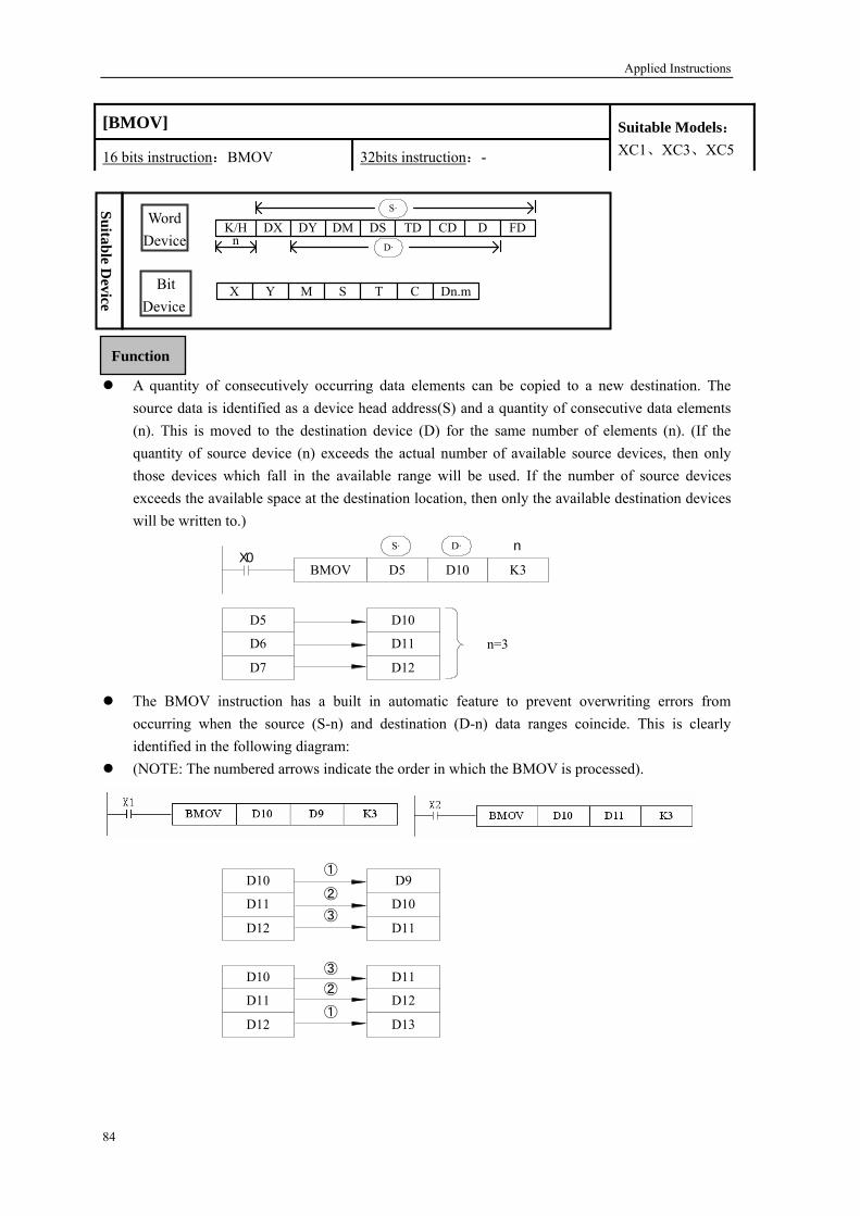
Applied Instructions
84
A quantity of consecutively occurring data elements can be copied to a new destination. The
source data is identified as a device head address(S) and a quantity of consecutive data elements (n). This is moved to the destination device (D) for the same number of elements (n). (If the quantity of source device (n) exceeds the actual number of available source devices, then only those devices which fall in the available range will be used. If the number of source devices exceeds the available space at the destination location, then only the available destination devices will be written to.)
BMOV D5 D10 K3X0
nS· D·
D5
D6
D7
D10
D11
D12
n=3
The BMOV instruction has a built in automatic feature to prevent overwriting errors from
occurring when the source (S-n) and destination (D-n) data ranges coincide. This is clearly identified in the following diagram:
(NOTE: The numbered arrows indicate the order in which the BMOV is processed).
D10
D11
D12
D9
D10
D11
D10
D11
D12
D11
D12
D13
①
②
③
③
②
①
Function
[BMOV]
16 bits instruction:BMOV 32bits instruction:-
Suitable Models: XC1、XC3、XC5
Suitable Device
S·Word
Device nD FDDMDX DY DS TD CDK/H
D·
Bit Device
X Y M S T C Dn.m
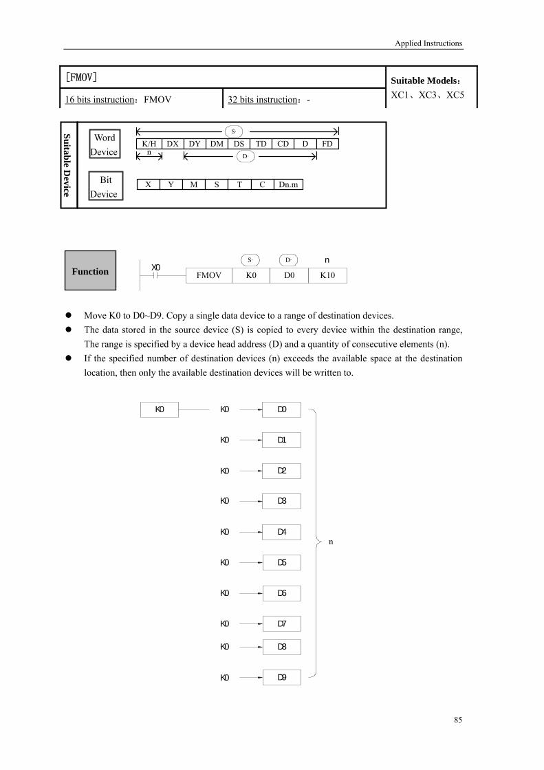
Applied Instructions
FMOV K0 D0 K10X0
nS· D·
Move K0 to D ~D9. Copy a single data device to a range of destination devices. The data stor opied to every device within the destination range,
The range is specified by a device head address (D) and a quantity of consecutive elements (n). If the specifie number of destination devices (n) exceeds the available space at the destination
location, then nly the available destination devices will be written to.
0ed in the source device (S) is c
d o
K0 D0K0
n
D1K0
D2K0
D3K0
D4K0
D5K0
D6K0
D7K0
D8K0
D9K0
Function
[FMOV]
16 bits instruction:FMOV 32 bits instruction:-
Suitable Models: XC1、XC3、XC5
Suitable Device
Word Device
Bit Device
X Y M S T C Dn.m
S·
D FDDMDX DY DS TD CDK/Hn D·
85

Applied Instructions
1, Written of a word
D0FWRT FD0X0
S· D·
2, Written of double word
D0DFWRT FD0X1
S· D·
3, Written of multi-word
D0FWRT FD0X2
K3
S· D1· D3·
Note:1, FWRT instruction only allow to write data into FlashROM register. In this storage area, even battery drop, data could be stored. So it could be used to store important technical parameters.
2, Written of FWRT needs a long time, about 150ms, so, frequently operate this operation is not recommended.
3, The written time of FlashROM is about 1,000,000 times. So, we suggest using edge signals (LDP、LDF etc.) to trigger.
※ Frequently written of FlashROM will ruin FlashROM forever.
[FWRT]
16 bits instruction:FWRT 32 bits instruction:DFWRT
Suitable Models: XC1、XC3、XC5
Function:write value in D0 into FD0
Function:write value in D0、D1 into FD0、FD1
Function:write value in D0、D2、D3 into FD0、FD1、FD2.
Function
Suitable Device
Word Device
Bit Device
X Y M S T C Dn.m
D·
S·
D FDDMDX DY DS TD CDK/H
86

Applied Instructions
ZRST M500 M559
D0 D100
D1· D2·
D1· D2·
X0
ZRST
MSET M10 M120
D1· D2·X0
X1RST M0
RST T0
RST D0
X2K0FMOV D0 K100
Function & Action
Zone Set Unit M10~M120
Zone Reset Bit Unit M500~M559。
Zone Reset Word Unit D0~D100
Other Reset Instruction
Reset M0
Reset the current value and status of T0
Reset the current value and status of C0
Write K0 into D0~D99
As soft unit’s separate reset instruction, RST instruction can be used to bit unit Y, M, S and word unit T, C, D.
As fill move for constant K0, 0 can be written into DX, DY, DM, DS, T, C, D.
Are specified as the same type of soft uniWhen > , only reset the soft unit specified in ts, and < D1· D2·D1· D1· D1·D2· D2·
[MSET]
16 bits instruction:MSET 32 bits instruction:-
Suitable Models: XC1、XC3、XC5
Word Device
Bit Device
X Y M S T C Dn.mD1· D2·
D FDDMDX DY DS TD CDK/H
[ZRST]
16 bits instruction:ZRST 32 bits instruction:-
Suitable Models: XC1、XC3、XC5
Word Device
Bit Device
X Y M S T C Dn.mD1· D2·
D FDDMDX DY DS TD CDK/HD1· D2·
87
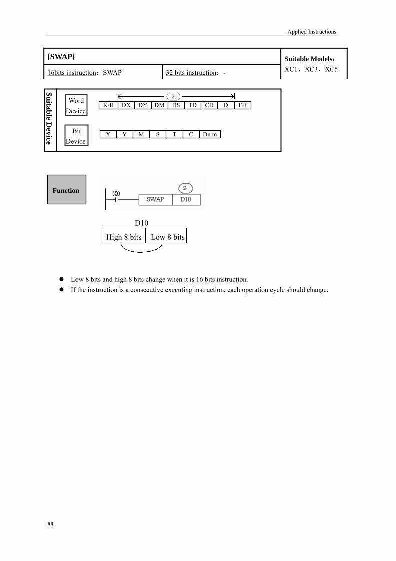
Applied Instructions
High 8 bits Low 8 bits
D10
Function
Low 8 bits and high 8 bits change when it is 16 bits instruction. If the instruction is a consecutive executing instruction, each operation cycle should change.
WAP] [S
16bits instruction:SWAP 32 bits instruction:-
Suitable Models: XC1、XC3、XC5
Suitable Device
Word Device
Bit
D FDDMDX DY DS TD CDK/HS·
X Y M S T C Dn.mDevice
88

Applied Instructions
[XCH]
1
《16 bits instruction》
6 bits instruction:XCH 32 bits instruction:DXCH
Suitable Models: XC1、XC3、XC5
Suitable Device
Word D
XCH D10 D11X0
D1· D2·
《32 bits instruction》
DXCH D10 D20X0
D1· D2·
Function
Device
Bit Device
X Y M S T C Dn.m
FDDMDX DY DS TD CDK/HD1· D2·
The contents of the two destination devices D1 and D2 are swapped,
When drive input X0 is ON each scan cycle should carry on data exchange
Before(D10)=100 →Aft
(D11)=101 0 er (D10)=101
(D11)=10
32 bits instruction [DXCH] swaps value composed by D10、D11 and the value
composed by D20 D21
89

Applied Instructions
90
5-6. Data Operation Instructions
Mnemonic Function ADD Addition SUB Subtraction MUL Multiplication DIV Division INC Increment DEC Decrement
MEAN Mean WAND Logic Word And WOR Logic Word Or
WXOR Logic Exclusive Or CML Compliment NEG Negation

Applied Instructions
ADD D10 D12 D14X0
S1· S2· D·
Function
The data contained within the two source devices are combined and the total is stored in the specified destination device. Each data’s highest bit is the sign bit, 0 stands for positive、1 stands for negative. All calculations are algebraic processed.(5+(-8)=-3)
If the result of a calculation is “0”, the “0” flag acts. If the result exceeds 323,767(16 bits limit)or 2,147,483,647(32 bits limit), the carry flag acts.(refer to the next page). If the result exceeds –323,768(16 bits limit)or –2,147,483,648(32 bits limit), the borrow flag
hen carry on 32 bits operation, word device’s low 16 bits are assigned, the device following closely the preceding device’s ID will be the high bits. To avoid ID repetition, we recommend you assign device’s ID to be even ID.
The same device may be used as a source and a destination. If this is the case then the result changes after every scan cycle. Please note this point.
(D10)+(D12)→(D14)
DD] Addition Operation [A
16 bits instruction:ADD 32 bits instruction:DADD
Suitable Models: XC1、XC3、XC5
Zero M8020 Borrow M8021
Flag Carry M8022
D FDDMDX DY DS TD CDK/HS1· S2·
D·
X Y M S T C Dn.m
Word Device
Bit Device
Suitable Device
acts(Refer to the next page) W
91
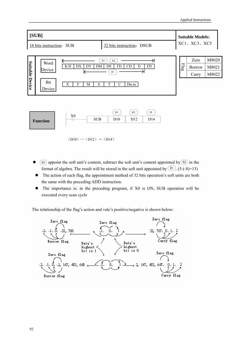
Applied Instructions
SUB D10 D12 D14X0
S1· S2· D·
The relationship of the flag’s action and vale’s positive/negative is shown below:
Function
(D10)—(D12)→(D14)
point th soft unit’s content, subtract the soft unit’s content appointed by in the format of algebra. The result will be stored in the soft unit appointed by (5-(-8)=13)
The action of ach flag, the appointment method of 32 bits operation’s soft units are both the same with the preceding ADD instruction.
The importance is: in the preceding program, if X0 is ON, SUB operation will be executed every scan cycle
ap e .
S1· S2·
D·
UB] [S
16 bits instruction:SUB 32 bits instruction:DSUB
Suitable Models: XC1、XC3、XC5
Zero M8020Borrow M8021
Flag Carry M8022
Suitable Device
Word Device
Bit Device
D FDDMDX DY DS TD CDK/HS1· S2·
D·
X Y M S T C Dn.m
e
92

Applied Instructions
《16 bits operation》
MUL D0 D2 D4X0
S1· S2· D·
《32 bits operation》
X1DMUL D0 D2 D4
S1· S2· D·
Function & action
BIN BIN BIN
(D0) × (D2) → (D5, D4)
16 bits 16 bits → 32 bits
BIN BIN BIN
(D1,D0) × (D3,D2) → (D7,D6,D5,D4)
32 bits 32 bits → 64 bits
The content of the two source devices are multiplied together and the result is stored at the destination device in the format of 32 bits. As in the upward chart: when (D0)=8、(D2)=9, (D5, D4) =72.
The result’s highest bit is the symbol bit: positive (0)、negative (1). When be bit unit, it can carry on the bit appointment of K1~K8. When appoint K4, only
the result’s low 16 bits can be obtained.
s
In 32 bits operation, when use bit device as the destination address, only low 32 bits result can be obtained. The high 32 bits result can not be obtained, so please operate again after transfer one time to the word device
Even use word device, 64 bits results can’t be monitored at once. In this situation, float point data operation is recommended.
[MUL]
16 bits instruction:MUL 32 bits instruction:DMUL
Suitable Models: XC1、XC3、XC5
Zero M8020Borrow M8021
Flag Carry M8022
Word Device
Bit Device
X Y M S T C Dn.m
D FDDMDX DY DS TD CDK/HS1· S2·
D·
93

Applied Instructions
《16 bits operation》
DIV D0 D2 D4X0
S1· S2· D·
《32 bits operation》
DDIV D0 D2 D4X1
S1· S2· D·
DDIV D0 D2 D4X1
S1· S2· D·
Function & Action
Dividend Divisor Result Remainder
BIN BIN BIN BIN
(D0) ÷ (D2) → D4) (D5)
16 bits 16 bits 16 bits 16 bits
Dividend Divisor Result Remainder
BIN BIN BIN BIN
(D1,D0) ÷ (D3,D2) (D5,D4) (D7,D6)
32 bits 32 bits 32 bits 32 bits
appoints the device’s content be the dividend, appoints the device’s content be the divisor ppoints the device and the next one to store the result and the remainder.
In the above example, if input X0 is ON, devision operation is executed every scan cycle.
, a
S1· S2·
D·
The dividend is composed by the device appointed by and the next one. The divisor is com osed by the device appointed by and the next one. The result and the remainder are stored in the four sequential devices, the first one is appointed by
If the value of the divisor is 0, then an operation error is executed and the operation of the DIV instruction is cancelled.
The highest bit of the result and remainder is the sym ol bit (positive:0, negative: 1). When any of the dividend or the divisor is negative, then the result will be negative. When the dividend is negative, then the remainder will be negative.
p
S1·
S2·
D·
[DIV]
16 bits instruction:DIV 32 bits instruction:DDIV
Suitable Models: XC1、XC3、XC5
Zero M8020Borrow M8021
Flag Carry M8022
Word Device
Bit Device
X Y M S T C Dn.m
D FDDMDX DY DS TD CDK/HS1· S2·
D·
b
94

Applied Instructions
INC D0
X0D·
DEC D0
X1D·
Function & Action
(D0)+1→(D0)
(D0)-1→(D0)
On every execution of the instruction the device specified as the destination has its current value incremented (increased) by a value of 1.
In 16 bits operation, when +32,767 is reached, the next increment will write -32,767 to the destination device. In this case, there’s no additional flag to identify this change in the counted value.
D·
On every execution of the instruction the device specified as the destination has its current value decremented (decreased) by a value of 1.
When -32,768 or -2,147,483,648 is reached, the next decrement will write +32,767 or +2,147,483,647 to the destination device.
D·
1、Increment [INC]
2、Decrement [DEC]
[INC] & [DEC]
16 bits instruction:INC、DEC 32 bits instruction:DINC、DDEC
Suitable Models: XC1、XC3、XC5
Zero M8020Borrow M8021
Flag Carry M8022
Word Device
Bit Device
X Y M S T C Dn.m
D FDDMDX DY DS TD CDK/HD·
95
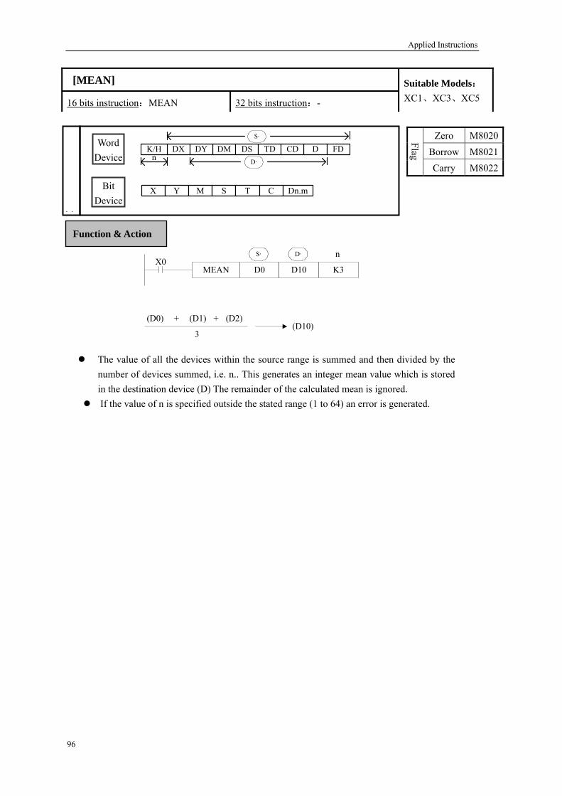
Applied Instructions
MEAN D0 D10 K3
S· D·X0
n
(D0) + +
3(D10)
(D1) (D2)
Function & Action
The value of all the devices within the source range is summed and then divided by the number of devices summed, i.e. n.. This generates an integer mean value which is stored in the destination device (D) The remainder of the calculated mean is ignored.
If the value of n is specified outside the stated range (1 to 64) an error is generated.
[MEAN]
16 bits instruction:MEAN 32 bits instruction:-
Suitable Models: XC1、XC3、XC5
Zero M8020Borrow M8021
Flag Carry M8022
Word Device
Bit Device
S·
nD FDDMDX DY DS TD CDK/H
D·
X Y M S T C Dn.m
96

Applied Instructions
Execute logic AND operation with each bit
WAND D10 D12 D14
D·X0
S1· S2·
Execute logic OR operation with each bit
WOR D10 D12 D14
D·X0
S1· S2·
Execute logic Exclusive OR operation with each bit.
WXOR D10 D12 D14
D·X0
S1· S2·
If use this instruction along with CML instruction, XOR NOT operation could also be executed.
Function & Action
0&0=0 0&1=0 1&0=0 1&1=1
0 or 0=0 0 or 1=1 1 or 0=1 1 or 1=1
0 xor 0=0 0 xor 1=1 1 xor 0=1 1 xor 1=0
[WAND]、 [WOR] & [WXOR]
16 bits instruction:WAND、WOR 32 bits instruction:DWAND、DWOR
Suitable Models: XC1、XC3、XC5
Zero M8020Borrow M8021
Flag Carry M8022
Word Device
Bit Device
D FDDMDX DY DS TD CDK/HS1· S2·
D·
Y M S T C Dn.mX
WXOR D10 D12 D14
D·X0
S1· S2·
CML D14 D14
97
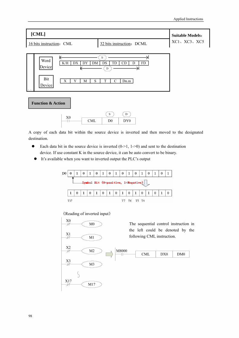
Applied Instructions
CML D0 DY0
S· D·X0
A copy of each data bit within the source device is inverted and then moved to the designated destination.
《Reading of inverted input》
M0
M1
M2
M3
M17
CML DX0 DM0M8000
X0
X1
X2
X3
X17
Function & Action
The sequential control instruction ithe left could be denoted by following CML instruction.
n the
Each data bit in the source device is inverted (0->1, 1->0) and sent to the destination device. If use constant K in the source device, it can be auto convert to be binary.
It’s available when you want to inverted output the PLC’s output
[CML]
16 bits instruction:CML 32 bits instruction:DCML
Suitable Models: XC1、XC3、XC5
Word Device
Bit Device
X Y M S T C Dn.m
D·
S·
D FDDMDX DY DS TD CDK/H
98

Applied Instructions
[NEG]
1
6 bits instruction:NEG 32 bits instruction:DNEG
Suitable Models: XC1、XC3、XC5
Word D FDDMDX DY DS TD CDK/H
D·
Device
Bit Device
X Y M S T C Dn.m
Functio ction n & A
NEG D10 (D10) +1 (D10)X0
D·
The bit format of the selected device is inverted, I.e. any occurrence of a “1’ becomes a “0” and any occurrence of “0” becomes “1”, when this is complete, a further binary 1 is added to the bit format. The result is the total logic sigh change of the selected devices contents.
99

Applied Instructions
5-7. Shift Instructions
Mnemonic Function SHL Arithmetic shift left SHR Arithmetic shift right LSL Logic shift left LSR Logic shift right ROL Rotation left ROR Rotation right SFTL Bit shift left SFTR Bit shift right WSFL Word shift left WSFR Word shift right
100
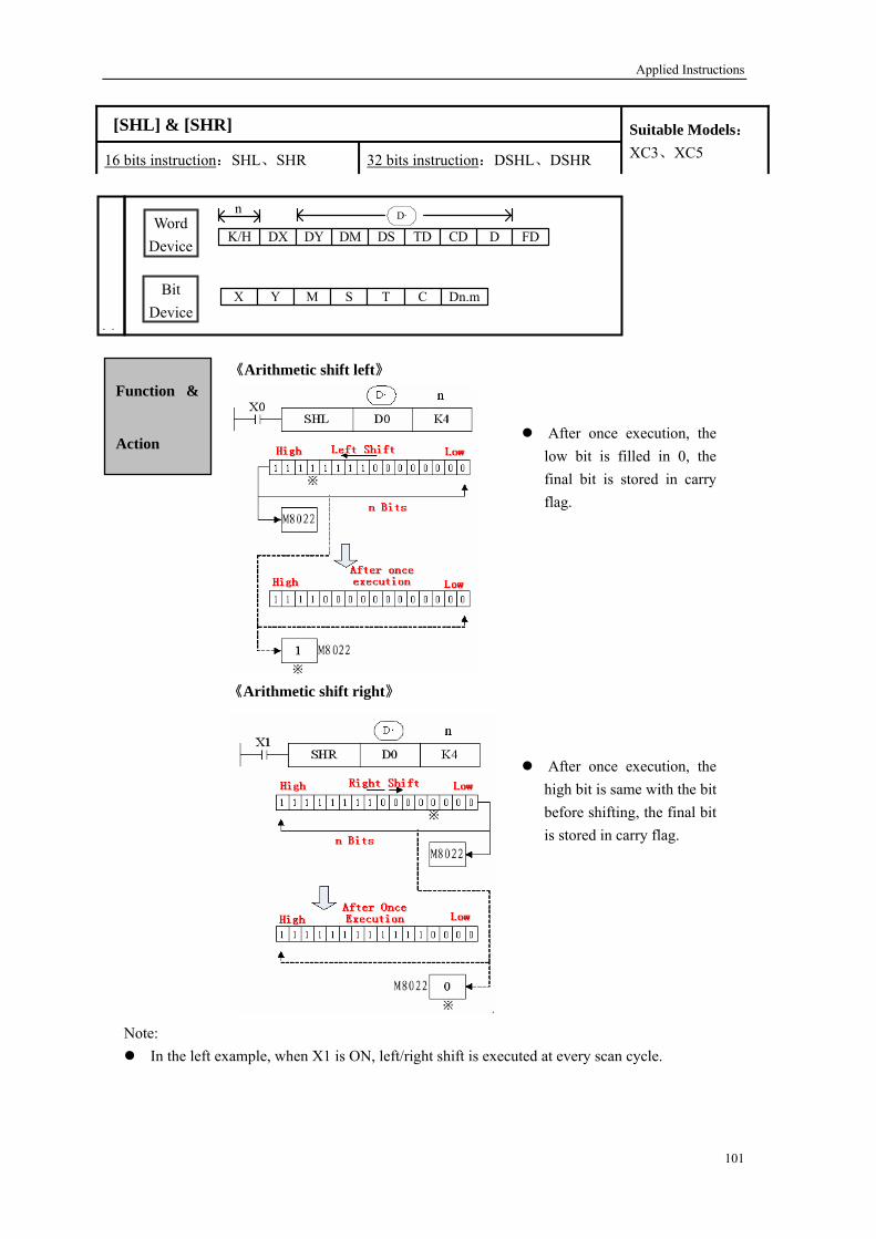
Applied Instructions
《Arithmetic shift left》
《Arithmetic shift right》
Function &
Action
After once execution, the high bit is same with the bit before shifting, the final bit is stored in carry flag.
After once execution, the low bit is filled in 0, the final bit is stored in carry flag.
[SHL] & [SHR]
16 bits instruction:SHL、SHR 32 bits instruction:DSHL、DSHR
Suitable Models: XC3、XC5
Note: In the left example, when X1 is ON, left/right shift is executed at every scan cycle.
Word Device
Bit Device
D FDDMDX DY DS TD CDK/HD·n
X Y M S T C Dn.m
101

Applied Instructions
《Logic shift left》
《Logic shift right》
Function & Action
After once execution, the low bit is filled in 0, the final bit is stored in carry flag.
After once execution, the high bit is same with the bit before shifting, the final bit is stored in carry flag.
NOTE: In every scan cycle, loop shift left/right action will be executed
[LSL] & LSR]
16 bits instruction: 32 bits instruction:DLSL、DLSR
Suitable Models: XC3、XC5
Word Device
Bit Device
D FDDMDX DY DS TD CDK/HD·n
X Y M S T C Dn.m
102
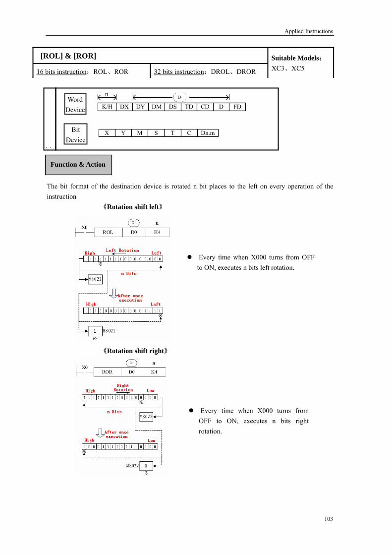
Applied Instructions
The bit format of the destination device is rotated n bit places to the left on every operation of the
struction 《Rotation shift left》
in
《Rotation shift right》
Function & Action
Every time when X000 turns from OFF to ON, executes n bits left rotation.
Every time when X000 turns from OFF to ON, executes n bits right rotation.
[ROL] & [ROR]
16 bits instruction:ROL、ROR 32 bits instruction:DROL、DROR
Suitable Models: XC3、XC5
Word Device
Bit Device
D FDDMDX DY DS TD CDK/HD·n
X Y M S T C Dn.m
103

Applied Instructions
Bit shift left》
《
《Bit shift right》
Function & Action
① M15~M12→Overflow
15~M 12
1~M8
M7~M4
→M3~M0
② M11~M 8→M
M1③ M 7~M 4→
→④ M 3~M 0
⑤ X 3~X 0
① M 3~M 0→Overflow
② M 7~M 4→M3~M0
③ M11~M 8→M7~M4
④ M15~M12→M11~M8
⑤ X 3~X 0→M15~M12
In every scan cycle, loop shift left/right action will be executed
[SFTL] & [SFTR]
16 bits instruction:SFTL、SFTR 32 bits instruction:DSFTL、DSFTR
Suitable Models: XC3、XC5
Word Device
Bit Device
The instruction copies n2 source devices to a bit stack of length n1. For every new addition of n2 bits, the existing data within the bit stack is shifted n2 bits to the left/right. Any bit data moving to the position exceeding the n1 limit is diverted to an overflow area. The bit shifting operation will occur every time the instruction is processed unless it is modified with either the pulse suffix or a controlled interlock.
D FDDMDX DY DS TD CDK/H
n1n2
X Y M S T C Dn.mD·
S·
104

Applied Instructions
《Word shift left》
105
n2 字左移
n2 字右移
《Word shift right》
Function & Action
The instruction copies n2 source devices to a word stack of length n1. For each addition of n2 words, the existing data within the word stack is shifted n2 words to the left/right. Any word data moving to a position exceeding the n1 limit is diverted to an overflow area. The word shifting operation will occur every time the instruction is processed unless it is modified with either the pulse suffix or a controller interlock.
① D13~D10→overflow
② D17~D14→D13~D10
③ D21~D18→D17~D14
④ D25~D22→D21~D18
⑤ D 3~D 0→D25~D22
In every scan cycle, loop shift left/right action will be executed
[WSFL] & [WSFR]
16 bits instruction:WSFL、WSFR 32 bits instruction:DWSFL、DWSFR
Suitable Models: XC3、XC5
Word Device
Bit Device
X Y M S T C Dn.m
D FDDMDX DY DS TD CDK/H
n1n2
D·
S·
① D25~D22→overflow
② D21~D18→D25~D22
③ D17~D14→D21~D18
④ D13~D10→D17~D14
⑤ D 3~D 0→D13~D10
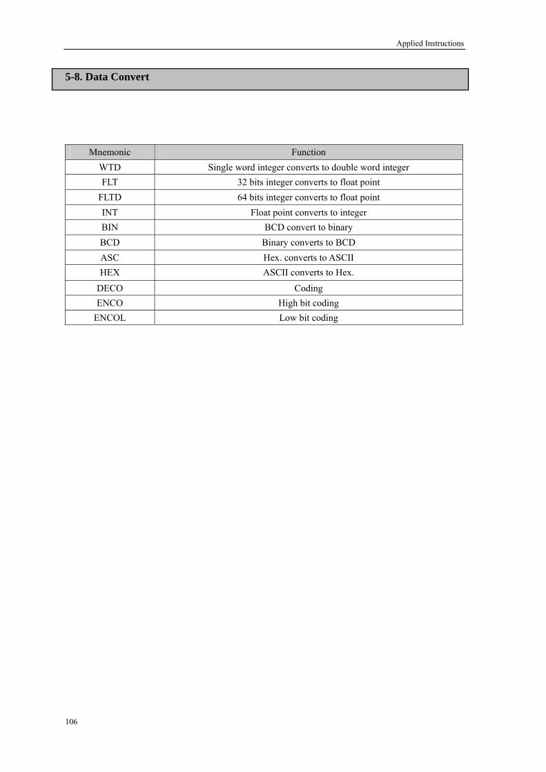
Applied Instructions
-8. Data Convert 5
Mnemonic Function WTD Single word integer converts to double word integer FLT 32 bits integer converts to float point
FLTD 64 bits integer converts to float point INT Float point converts to integer BIN BCD convert to binary BCD Binary converts to BCD ASC Hex. converts to ASCII HEX ASCII converts to Hex.
DECO Coding ENCO High bit coding
ENCOL Low bit coding
106
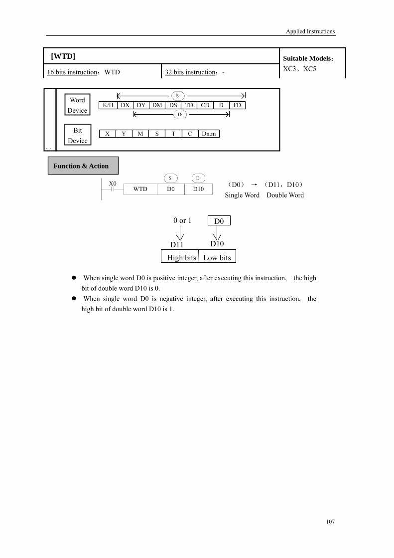
Applied Instructions
WTD D0 D10X0
S· D·
High bits Low bits
D11 D10
0 or 1 D0
Function & Action
(D0) → (D11,D10) Single Word Double Word
When single word D0 is positive integer, after exe ing this instruction, the high bit of double word D10 is 0.
When single word D0 is negative integer, after executing this instruction, the high bit of double word D10 is 1.
[WTD]
16 bits instruction:WTD 32 bits instruction:-
Suitable Models: XC3、XC5
Word Device
Bit Device
X Y M S T C Dn.m
D FDDMDX DY DS TD CDK/HS·
D·
cut
107

Applied Instructions
《16 Bits》
《32 Bits》
DFLT D10 D12
S· D·X0
《64 Bits》
FLTD D10 D14
S· D·X0
Function & Action
(D11,D10)→ (D13,D12)
BIN integer Binary float point
(D10) → (D13,D12)
BIN integer Binary float point
Convert BIN integer to binary float point. As the constant K、H will auto convert by the float operation instruction, so this FLT instruction can’t be used.
The instruction is contrary to INT instruction.
(D13,D12,D11,D10)→ (D17,D16,D15,D14)
BIN integer Binary float point
FLT D10 D12
S· D·X0
[FLT] & [FLTD]
16 bits instruction:FLT 32 bits instruction:DFLT
Suitable Models: XC3、XC5
Word Device
Bit Device
X Y M S T C Dn.m
D FDDMDX DY DS TD CDK/HD·
S· S·
108

Applied Instructions
《16 位》
INT D10 D20
S· D·X0
《32 位》
DINT D10 D20
S· D·X0
Function & Action
(D11,D10) → (D20)
Binary Floating BIN integer
Give up the data after the decimal dot
(D11,D10) → (D20,D21)
Binary Floating BIN integer
Give up the data after the decimal dot
The binary source number is converted into an BIN integer and stored at the destination device. Abandon the value behind the decimal point. This instruction is contrary to FLT instruction. When the result is 0, the flag bit is ON。 When converting, less than 1 and abandon it, zero flag is ON. 16 bits operation:-32,768~32,767 32 bits operation:-2,147,483,648~2,147,483,647
[INT]
16 bits instruction:- 32 bits instruction:INT
Suitable Models: XC3、XC5
Word Device
Bit Device
D FDDMDX DY DS TD CDK/HD·
S·
X Y M S T C Dn.m
109

Applied Instructions
BIN D10 D0
S· D·
X0
Function & Action
Convert and move instruction of Source (BCD) → destination (BIN)
When source data is not BCD code, M8067(Operation error), M8068 (Operation error lock) will not work.
As constant K a a ll nv t a o n it this in
[BIN]
utom tica y co erts o bin ry, s it’s ot su able forstruction.
16 bits instruction:BIN 32 bits instruction:-
Suitable Models: XC3、XC5
Word Device
D FDDMDX DY DS TD CDHS·
K/D·
Bit Device
X Y M S T C Dn.m
110

Applied Instructions
BCD D10 D0
S· D·X0
Function & Action
Convert and move instruction of source (BIN)→destination (BCD).
This instruction can be used to output data directly to a seven-segment display.
[BCD]
16 bits instruction:BCD 32 bits instruction:-
Suitable Models: XC3、XC5
Word Device
X Y M S T C Dn.m
D FDDMDX DY DS TD CDK/HD·
S·
Bit Device
111
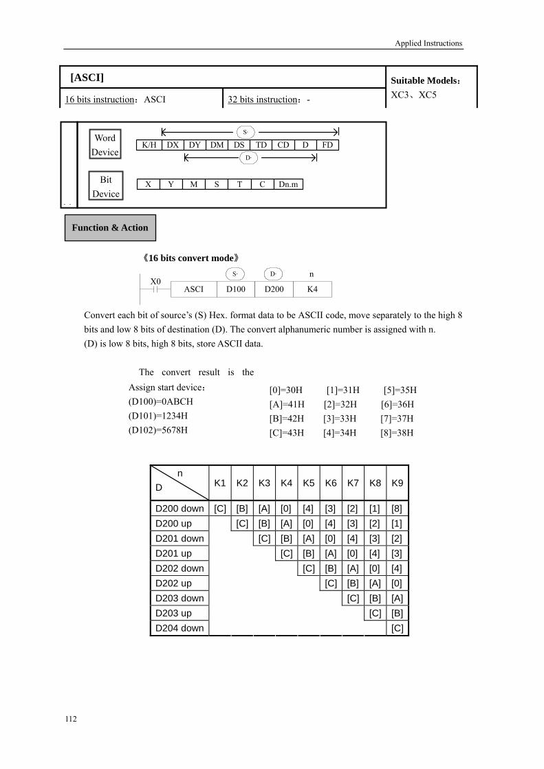
Applied Instructions
《16 bits convert mode》
ASCI D100 D200 K4
S· D· nX0
Convert each bit source’s (S) Hex. format data to be ASCII code, move separately to the high 8 bits and low 8 bits of destination (D). The convert alphanumeric number is assigned with n. (D) is low 8 bits, high 8 bits, store ASCII data.
The convert result is the following:
n D K1 K2 K3 K4 K5 K6 K7 K8 K9
of
D200 down [C] [B] [A] [0] [4] [3] [2] [1] [8] D200 up [C] [B] [A] [0] [4] [3] [2] [1] D201 down [C] [B] [A] [0] [4] [3] [2] D201 up [C] [B] [A] [0] [4] [3] D202 down [C] [B] [A] [0] [4] D202 up [C] [B] [A] [0] D203 down [C] [B] [A] D203 up [C] [B] D204 down
[C]
Function & Action
Assign start device: (D100)=0ABCH (D101)=1234H (D102)=5678H
[0]=30H [1]=31H [5]=35H [A]=41H [2]=32H [6]=36H [B]=42H [3]=33H [7]=37H
H [4]=34H [8]=38H
[ASCI]
16 bits instruction:ASCI 32 bits instruction:-
Suitable Models: XC3、XC5
Word Device
Bit Device
X Y M S T C Dn.m
D FDDMDX DY DS TD CDK/HD·
S·
[C]=43
112

Applied Instructions
113
《16 bits switch mode》
HEX D200 D100 K4
S· D· nX0
The convert of the upward program is the following: 时
n=k4
0 1 0 0 0 0 0 1 0 0 1 1 0 0 0 0D200
41H→[A] 30H→[0]
0 1 0 0 0 0 1 1 0 1 0 1 0 0 1 0D201
43H→[C] 42H→[B]
0 0 0 0 1 0 1 0 1 0 1 1 1 1 0 0D202
0 A B C
Function & Action
(S·)
ASCII Code
HEX Convert
D200 down 30H 0 D200 up 41H A D201 down 42H B D201 up 43H C D202 down 31H 1 D202 up 32H 2 D203 down 33H 3 D203 up 34H 4 D204 down 35H 5
(D·)
nD102 D101 D100
1 ···0H 2 ··0AH 3 ·0ABH4
Not change to be 0
0ABCH 5 ···0H ABC1H 6 ··0AH BC12H 7 ·0ABH C123H 8
0ABCH 1234H 9 ···0H ABC1H 2345H
Convert the gh and low 8 bits in source to HEX data. Move 4 bits every time to destination. The convert alphanumeric number is assigned by n.
[HEX]
16 bits instruction:HEX 32 bits instruction:-
Suitable Models: XC3、XC5
Word Device
Bit Device
X Y M S T C Dn.m
D FDDMDX DY DS TD CDK/HD·
S·
hi
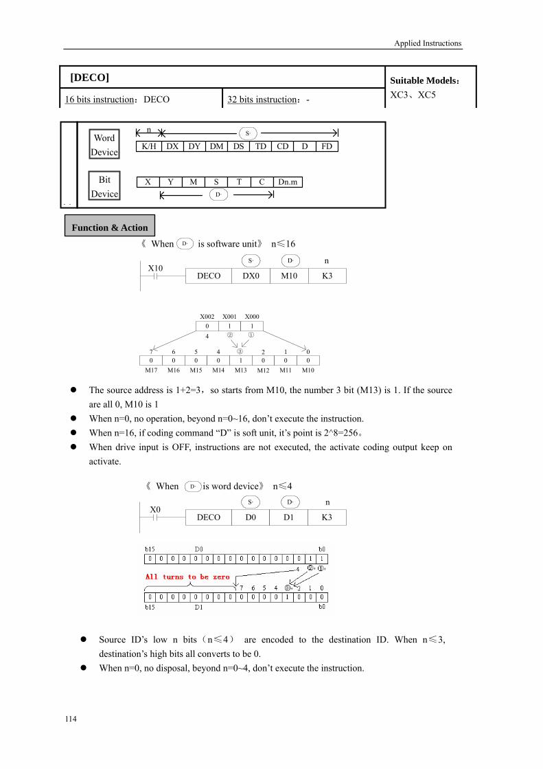
Applied Instructions
①②
③
《 When is software unit》 n≤16
DX0DECO M10 K3X10
nS· D·
0 1 1
0 0 0 1 0 0 0
X002 X001 X000
M17 M16 M15 M14 M13 M12 M11 M10
1 0
4
7 6 5 4 20
《 When is word device》 n≤4
③
D0DECO D1 K3X0
nS· D·
Function & Action D·
The source address is 1+2=3,so starts from M10, the number 3 bit (M13) is 1. If the source are all 0, M10 is 1
When n=0, no operation, beyond n=0~16, don’t execute the instruc on. When n=16, if coding command “D” is soft unit, it’s point is 2^8=256。 When drive in ut is OFF, instructions are not executed, the activate coding output keep on
activate.
ti
p
D·
Source ID’s low n bits(n≤4) are encoded to the destination ID. When n≤3, destination’s high bits all converts to be 0.
When n=0, no disposal, beyond n=0~4, don’t execute the instruction.
[DECO]
16 bits instruction:DECO 32 bits instruction:-
Suitable Models: XC3、XC5
Word Device
Bit Device
X Y M S T C Dn.mD·
S·n
D FDDMDX DY DS TD CDK/H
114

Applied Instructions
[ENCO]
1
③
③
①②
①②
All be 0
All be 0
Be ignored
《 When is bit device》 n≤16
6 bits instruction:ENCO 32 bits instruction:-
Suitable Models: XC3、XC5
Word Device
D FDDMDX DY DS TD CDK/HD·n
S·
Bit X Y M S T C Dn.mDevice S·
Funct ction ion & A
M10ENCO D10 K3X0
nS· D·
0 0 0 1 0 1 0M17 M16 M15 M14 M13 M12 M11 M10
7 6 5 4 2 1 00
0 0 0 0 0 0 0 0 0 0 0 0 0 0 1 1D10b15
b0
4
《 When is word device》 n≤4
D0ENCO D1 K3X1
nS· D·
0 1 0 1 0 1 0 1 0 0 0 0 1 0 1 0
0 0 0 0 0 0 0 0 0 0 0 0 0 0 1 1
7 6 5 4 2 1 0
D0
D1b15
b15 b0
b0
4
S·
S·
If many bits in the source ID are 1, ignore the low bits. If source ID are all 0, don’t execute the instructions.
When drive input is OFF, the instruction is not executed, encode output don’t change. When n=8, if encode instruction’s “S” is bit unit, it’s point number is 2^8=256
115

Applied Instructions
③
③
①②
①②
All be 0
All be 0
Be ignored
《 If is bit device》 n≤16
M10ENCOL D10 K3X0
nS· D·
0 1 0 1 0 0 0M17 M16 M15 M14 M13 M12 M11 M10
7 6 5 4 2 1 00
0 0 0 0 0 0 0 0 0 0 0 0 0 0 1 1D10b15
b0
4
《 是字软元件时》 n≤16
D0ENCOL D1 K3X1
nS· D·
0 1 0 1 0 1 0 1 0 0 1 0 1 0 0 0
0 0 0 0 0 0 0 0 0 0 0 0 0 0 1 1
7 6 5 4 2 1 0
D0
D1b15
b15 b0
b0
4
S·
S·
If many bits in the source ID are 1, ignore the high bits. If source ID are all 0, don’t execute the instructions.
When drive input is OFF, the instruction is not executed, encode output don’t change. When n=8, if encode instruction’s “S” is bit unit, it’s point number is 2^8=256
Function & Action
[ENCOL]
16 bits instruction
Word Device
Bit Device
X Y M S T C Dn.mS·
S·
D FDDMDX DY DS TD CDK/HD·n
:ENCOL 32 bits instruction:-
Suitable Models: XC3、XC5
116
Applied Instructions
5-9. Floating Operation
Mnemonic Function ECMP Float Compare EZCP Float Zone Compare EADD Floa Addt ESUB Float Subtract EMUL ltiplication Float MuEDIV Float Division ESQR Float Square Root SIN Sine COS Cosine TAN Tangent
117

Applied Instructions
ECMP D10 D20 M0
M0
M1
M2
X0D·S1· S2·
ECMP K500 D100 M10X0
Function & Action
(D11,D10) : (D21,D20)→M0,M1,M2 Binary Floating Binary Floating
(D11, D10) > (D21<D20)
Binary Floating Binary Floating
(D11, D10) = (D21<D20)
Binary Floating Binary Floating
(D11, D10) < (D21<D20)
Binary Floating Binary Floating
The status of the destination device will be kept even if the ECMP instruction is deactivated.
The binary float data of S1 is compared to S2. The result is indicated by 3 bit devices specified with the head address entered as D.
If a constant K or H used as source data, the value is converted to floating point before the addition operation.
(K500) ∶ (D101,D100)→M10,M11,M12
Binary converts Binary floating
to floating
[ECMP]
16 bits instruction:- 32 bits instruction:ECMP
Suitable Models: XC3、XC5
Word Device
Bit Device
X Y M S T C Dn.mD·
D FDDMDX DY DS TD CDK/H
S1· S2· S1· S2·
118

Applied Instructions
Compare a float range with a float value.
EZCP D10 D20 D0
M3
M4
M5
X0S1· S2·
M3
D1· D2·
The data of S1 is compared to the data of S2. The result is indicated by 3 bit devices specified with the head address entered as D.
If a constant K or H used as source data, the value is converted to floating point before the addition operation.
EZCP K10 K2800 D5 M0X0
lease set S1<S2, when S2>S1, see S2 as the same with S1 and compare them.
P
Function & Action
(D20, D21) > (D1, D0) ON
Binary Floating Binary Floating
(D21,D10) ≤ (D1,D0) ≤ (D31,D30) ON
Binary Floating Binary Floating Binary Floating
(D1, D0) > (D31, D30) ON
Binary Floating Binary Floating
The status of the destination device will be kept even if the EZCP instruction is deactivated.
(K10) ∶ [D6,D5] ∶ (K2800)→M0,M1,M2
Binary converts Binary Floating Binary converts
to Floating to Floating
[EZCP]
16 bits instruction:- 32 bits instruction:ECMP
Suitable Models: XC3、XC5
Word Device
Bit Device
D FDDMDX DY DS TD CDK/H
S1· S2· S3·
S1· S2· S3·
X Y M S T C Dn.mD·
119

Applied Instructions
EAAD D10 D20 D50
S1· S2· D·X0
EAAD D100 K1234 D110X1
Function & Action
(D11,D10) + (D21,D20) → (D51,D50)
Binary Floating Binary Floating Binary Floating
The floating point values stored in the source devices S1 and S2 are algebraically added and the result stored in the destination device D.
If a constant K or H used as source data, the value is converted to floating point before the addition operation.
(K1234) + ( D101,D100) → (D111,D110)
Binary converts to Floating Binary Floating Binary Floating
The same device may be used as a source and as the destination. If this is the case then, on continuous operation of the EADD instruction, the result of the previous operation will be used as a new source value and a new result calculated. This will happen every program scan unless the pulse modifier or an interlock program is used.
[EADD]
16 bits instruction:- 32 bits instruction:EADD
Suitable Models: XC3、XC5
Word Device
Bit Device
D FDDMDX DY DS TD CDK/HS1· S2· S2·
D·
S1·
X Y M S T C Dn.m
120

Applied Instructions
ESUB D10 D20 D50
S1· S2· D·X0
The floating point value of S2 is subtracted from the floating point value of S1 and the result stored in destination device D.
If a constant or H used as source data, the value is converted to floating point before the addition operation.
K
ESUB D100K1234 D110X1
Function & Action
(D11,D10) - (D21,D20) → (D51,D50)
Binary Floating Binary Floating Binary Floating
(K1234) - (D101,D100) → (D111,D110)
Binary converts to Floating Binary Floating Binary Floating
The same device may be used as a source and as the destination. If this is the case then, on continuous operation of the EADD instruction, the result of the previous operation will be used as a new source value and a new result calculated. This will happen every program scan unless the pulse modifier or an interlock program is used.
[ESUB]
16 bits instruction:- 32 bits instruction:ESUB
Suitable Models: XC3、XC5
D FDDMDX DY DS TD CDK/H
S1· S2· S2·
D·
S1·
Word Device
Bit Device
X Y M S T C Dn.m
121

Applied Instructions
122
EMUL D10 D20 D50
S1· S2· D·X0
EMUL D100K100 D110X1
Function & Action
(D11,D10) × (D21,D20) → (D51,D50)
Binary Floating Binary Floating Binary Floating
The floating value of S1 is multiplied with the floating value point value of S2. The result of the multiplication is stored at D as a floating value.
If a constant K or H used as source data, the value is converted to floating point before the addition operation.
(K100) × (D101,D100) → (D111,D110)
Binary converts to Floating Binary Floating Binary Floating
[EMUL]
16 bits instruction:- 32 bits instruction:EMUL
Suitable Models: XC3、XC5
Word Device
Bit Device
X Y M S T C Dn.m
D FDDMDX DY DS TD CDK/HS1· S2· S2·
D·
S1·

Applied Instructions
EDIV D10 D20 D50
S1· S2· D·X0
The floating point value of S1 is divided by the floating point value of S2. The result of the division is stored in D as a floating point value. No remainder is calculated.
If a constant K or H used as source data, the value is converted to floating point before the addition operation.
EDIV D100 K100 D110X1
Function & Action
(D11,D10)÷(D21,D20)→(D51,D50)
Binary Floating Binary Floating Binary Floating
(D101,D100) ÷ (K100) → (D111,D110)
Binary Floating Binary converts to Floating Binary Floating
If S2 is zero then a divide by zero error occurs and the operation fails.
[EDIV]
16 bits instruction:- 32 bits instruction:EDDIV
Suitable Models: XC3、XC5
Word Device
Bit Device
D FDDMDX DY DS TD CDK/HS1· S2· S2·
D·
S1·
X Y M S T C Dn.m
123

Applied Instructions
ESQR D10 D20X0
S· D·
ESQR K1024 D110X1
Function & Action
(D11,D10) →(D21,D20)
Binary Floating Binary Floating
A square root is performed on the floating point value in S the result is stored in D. If a constant K or H used as source data, the value is converted to floating point before
the addition operation.
(K1024) → (D111,D110)
Binary converts to Floating Binary Floating
When the result is zero, zero flag activates Only when the source data is positive will the operation be effective. If S is negative then
an error occurs and error flag M8067 is set ON, the instruction can’t be executed.
[ESQR]
16 bits instruction: 32 bits instruction- :ESQR
Suitable Models: XC3、XC5
Word Device
Bit Device
X Y M S T C Dn.m
D FDDMDX DY DS TD CDK/HD·
S· S·
[SIN]
16 bits instruction: 32 bits instruction- :SIN
Suitable Models: XC3、XC5
124

Applied Instructions
SIN D50 D60X0
S· D·
D51 D50
D61 D60
S·
D·
Function & Action
(D51,D50) → (D61,D60)SIN
Binary Floating Binary Floating
This instruction performs the mathematical SIN operation on the floating point value in S (angle RAD). The result is stored in D.
RAD value (angle×π/180)
Assign the binary floating value
SIN value
Binary Floating
[COS]
16 bits instruction:- 32 bits instruction:COS
Suitable Models: XC3、XC5
Word Device
Bit Device
D FDDMDX DY DS TD CDK/HD·
S· S·
X Y M S T C Dn.m
125
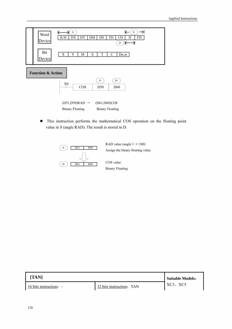
Applied Instructions
COS D50 D60X0
S· D·
D51 D50
D61 D60
S·
D·
Functi tion on & Ac
(D51,D50)RAD → (D61,D60)COS
Binary Floating Binary Floating
This instruction performs the mathematical COS operation on the floating point value in S (angle RAD). The result is stored in D.
RAD value (angle×π/180)
Assign the binary floating value
COS value
Binary Floating
[TAN]
16 bits instruction:- 32 bits instruction:TAN
Suitable Models: XC3、XC5
D FDDMDX DY DS TD CDK/HD·
S·S·Word
Device
Bit Device
X Y M S T C Dn.m
126

Applied Instructions
Word Device
Bit Device
X Y M S T C Dn.m
D FDDMDX DY DS TD CDK/HD·
S· S·
TAN D50 D60X0
S· D·
D51 D50
D61 D60
S·
D·
Function & Action
(D51,D50)RAD → (D61,D60)TAN
Binary Floating Binary Floating
This instruction performs the mathematical TAN operation on the floating point value in S. The result is stored in D.
RAD value (angle×π/180)
Assign the binary floating value
TAN value
Binary Floating
127

Applied Instructions
5-10. Clock Operation
Mnemonic Function TCMP Time Compare TZCP Time Zone Compare TADD Time Add TSUB Time Subtract TRD Read RTC data TWR Set RTC data
N :The models without clock can not use these instructions. ote
128

Applied Instructions
Function & Action
Compare the assigned time with time data.
The status of the destination devices is kept, even if the TCMP instruction is deactivated.
:Assign the compare standard “Hour” :Assign the compare standard “Minute” :Assign the compare standard “Second”
S1·
S2·
S3·
「 , , 」represent hours, minutes and seconds respectively. This time is compared to the time value in the 3 data devices specified by the head address , The result is indicated in the 3 bit devices specified by the head address
S1· S2· S3·
S·
D·
:Assign the “Hour” of clock data +1 :Assign the “Minute” of clock data +2 :Assign the “Second” of clock data
S ·
S ·
S ·
, + 2 :According to the compare result, the 3 devices output ON/OFF.
The valid range of “Hour” is「0~23」. The valid range of “Minute” is「0~59」. The valid range of “Second” is「0~59」.
1, +
D· D· D·
Time Compare [TCMP]
16 bits instruction:DIV 32 bits instruction:DDIV
Suitable Models: XC3、XC5
Word Device
Bit Device
D FDDMDX DY DS TD CDK/HS1· S2· S3·
S·
X Y M S T C Dn.mD·
129

Applied Instructions
130
Function & Action
即使使用 X000=OFF 停止执行 TZCP 指令时,M0~M2
仍然保持 X000 变为 OFF 以前的状态。
Compare the two assigned time with time data
Compare the 3 clock data start from with the two ends on the clock compare bound, according to the area bound, output the three ON/OFF status starts from
S·
D·
+1 2 : Assign the compare low limit in the form of “Hour”, “Minute” and “Second”. + 2 : Assign the compare low limit in the form of “Hour”, “Minute” and “Second”. +1 +2 : Assign the clock data in the form of “Hour”, “Minute” and “Second”.
+1 +2 : According to the compare result, the 3 devices output ON/OFF.
S1· , , + , 1, +
S1· S1·
S2·
, ,
S2·S2·
S·, ,
S· S·
D·D·D·
The valid range of “Hour” is「0~23」. The valid range of “Minute” is「0~59」. The valid range of “Second” is「0~59」.
[TZCP]
16 bits instruction:DIV 32 bits instruction:DDIV
Suitable Models: XC3、XC5
Word Device
Bit Device
The status of the destination devices is kept, even if the TCMP instruction is deactivated.
X Y M S T C Dn.mD·
D FDDMDX DY DS TD CDK/HS1· S2· S3·

Applied Instructions
D10 (Hour)D11 (Minute)
D12 (Second)
D20 (Hour)D21 (Minute)
D22 (Second)
D30 (Hour)D31 (Minute)
D32 (Second)+
S1 S2 D
10 hour 20 min. 30 sec. 3 hour 20 min. 10 sec. 13 hour 40 min. 40 sec.
18 (Hour)10 (Minute)
30 (Second)
10 (Hour)20 (Minute)
5 (Second)
4 (Hour)30 (Minute)
35 (Second)+
S1 S2 D
18 hour 10 min. 30 sec. 3 hour 20 min. 10 sec. 4 hour 30 min. 35 sec.
Function & Action
Each of S1, S2 and D specify the head address of 3 data devices to be used a time value. The time value in S1 is added to the value in S2, the result is stored to D as a new time value.
If the addition of the two times results in a value greater than 24 hours, the value of the result is the time remaining above 24 hours. When this happens the carry flag M8022 is
When the result is 0(0 Hour 0 Minute 0 Second),Set zero flag ON.
The valid range of “Hour” is「0~23」. The valid range of “Minute” s「0~59」. The valid range of “Second” is「0~59」.
(D10, D11, D12)+(D20, D21, D22)→(D30, D31, D32)
TADD D10 D20 D30X0
S1· S2· D·
[TADD]
16 bits instruction:DIV 32 bits instruction:DDIV
Suitable Models: XC3、XC5
Word Device
Bit Device
D FDDMDX DY DS TD CDK/HS1· S2·
D·
X Y M S T C Dn.m
i
131

Applied Instructions
TSUB D10 D20 D30X0
S1· S2· D·
D10 (Hour)
D11 (Minute)
D12 (Second)
D10 (Hour)
D11 (Minute)
D12 (Second)
D10 (Hour)
D11 (Minute)
D12 (Second)_ =
S1 S2 D
10 hour 20 min. 30 sec. 3 hour 20 min. 10 sec. 7 hour 0 min. 20 sec.
10 (Hour)
20 (Minute)
5 (Second)
18 (Hour)
10 (Minute)
30 (Second)
4 (Hour)
30 (Minute)
35 (Second)_ =
S1 S2 D
10 hour 20 min. 5 sec. 18 hour 10 min. 30 sec. 4 hour 30 min. 35 sec.
Function & Action
Each of S1, S2 and D specify the head address of 3 data devices to be used a time value. The time value in S1 is subtracted from the time value in S2, the result is stored to D as a new time.
If the subtraction of the two times results in a value less than 00:00:00 hours, the value of the result is the time remaining below 00:00:00 hours. When this happens the borrow flag M8021 is set ON.
When the result is 0 (0 hour 0 min. 0 sec.), zero flag set ON.
The valid range of “Hour” is「0~23」. The valid range of “Minute” is「0~59」. The valid range of “Second” is「0~59」.
(D10, D11, D12)-(D20, D21, D22)→(D30, D31, D32)
[TSUB]
16 bits instruction:DIV 32 bits instruction:DDIV
Suitable Models: XC3、XC5
Word Device
Bit Device
X Y M S T C Dn.m
D FDDMDX DY DS TD CDK/HS1· S2·
D·
132

Applied Instructions
TRD D0X0
D·
Function & Action The current time and date of the real time clock are read and stored in the 7 data devices specified by the head address D.
Read PLC’s real time clock according to the following format. The reading source is the special data register (D8013~D8019)which save clock data.
[TRD]
16 bits instruction:DIV 32 bits instruction:DDIV
Suitable Models: XC3、XC5
Word Device
Bit Device
X Y M S T C Dn.m
D FDDMDX DY DS TD CDK/HD·
Unit Item Clock data
D8018 Year 0-99
D8017 Month 1-12
D8016 Date 1-31
D8015 Hour 0-23
D8014 Minute 0-59
D8013 Second 0-59
Special data register for real
time clock t
D8019 Week 0 (Sun.)-6 (Sat.)
Unit Item
D0 Year
D1 Month
D2 Date
D3 Hour
D4 Minute
D5 Second
D Week
133
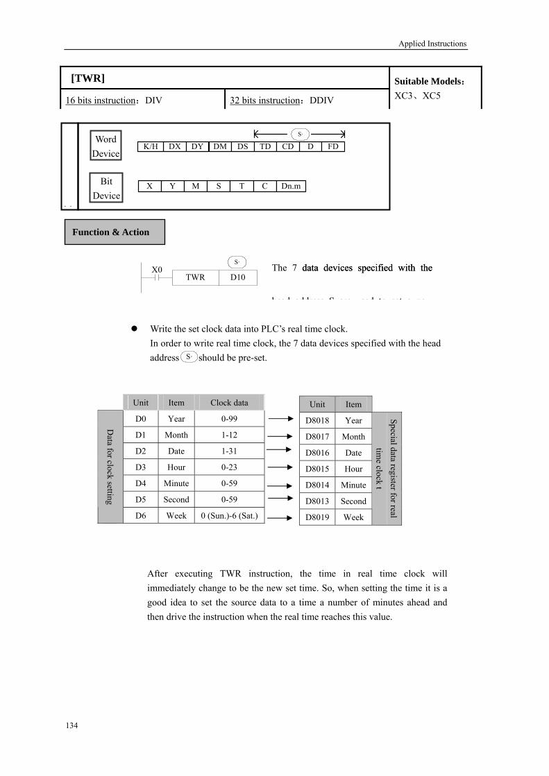
Applied Instructions
[TWR]
16 bits instruction:DIV 32 bits instruction:DDIV XC3、XC5
Suitable Models:
TWR D10X0
S·
Function & Action
The 7 data devices specified with the data devices specified with the
head address S are sed to set a ne
Write th ck data into PLC’s real time clock. In order real time clock, the 7 data ead address ld be pre-set.
e set clo to write devices specified with the h
shouS·
After e TWR instruction, the will immedia to be the new set time. t is a good idea to set the source data to a time a number utes ahead and then driv ruction when the real time reache
xecuting time in real time clock tely change So, when setting the time i
of mine the inst s this value.
D FDDMDX DY DS TD CDK/HWord
Device
Bit Device
S T C Dn.mX Y M
S·
Unit Item Clock data
D0 Ye 0-99 ar
D1 Month 1-12
D2 Date 1-31
D3 H 0-23 our
D4 Mi 0-59 nute
D5 Sec 0-59 ond
Data for clock setting
D6 Wee un.)-6 (Sat.) k 0 (S
Unit Item
D8018 Year
D8017 Month
D8016 Date
D8015 Hour
D8014 Minute
D8013 Second
D8019 Week
Specd
ial ata register for real
time clock t
134

Applied Instructions
In this chapter, we describe applied instruction’s function of XC C. series PL
5. Applied Instruction
s
5-1.Table of Appl ctions ied Instru
5-2.Reading Met pplied Instructions hod of A
5-3.Flow Instructions
5-4.Contactors Compare Instructions
5-5.Move and Compare Instructions
5-6.Arithmetic and Logic Operation Instructions
5-7.Loop and Shift Instructions
5-8.Data Convert
5-9.Floating Operation
5-10.Clock Operation
135

Applied Instructions
5-1. Applied Instruction List The applied instructions’ sort and their correspond instru following table: Common statements 1/XC3/XC5:
ctions are listed in the
of XC
Sort Mnemonic Function CJ n jump Conditio
CALL Call subroutine SRET Subroutine return STL Flow start
STLE Flow end SET nt flow Open the assigned flow, close the curre
ST se the current Open the assigned flow, not clo
flow FOR T loop Start of a FOR-NEX
NEXT EXT loop End of a FOR-N
Program Flow
FEND First end LD= (S1) = (S2) LD activates ifLD> LD activates if (S1) > (S2) LD< tes if (S1) =< (S2) LD activa
LD<> f(S1)≠(S2) LD activates iLD<= f(S1)≤(S2) LD activates iLD>= tes if(S1)≥(S2) LD activaAND= s if(S1)=(S2) AND activateAND> tivates if(S1)>(S2) AND acAND< ates if(S1)<(S2) AND activ
AND<> s if(S1)≠(S2) AND activateAND<= ates if(S1)≤(S2) AND activAND>= es if(S1)≥(S2) AND activat
OR= OR activates if(S1)=(S2) OR> OR activates if(S1)>(S2) OR< OR activates if(S1)<(S2)
OR<> OR activates if(S1)≠(S2) OR<= OR activates if(S1)≤(S2)
Data C
OR>= OR tes if(S1)≥(S2)
ompare
activaMOV Move
BMOV Block move FMOV Fill move FWRT FlashROM written MSET Zone set
Data Move
ZRST Zone reset
136

Applied Instructions
SWAP The high and low byte of the destinated devices
are exchanged XCH Exchange ADD Addition SUB Subtraction MUL Multiplication DIV Division INC Increment DEC Decrement
MEAN Mean WAND Word And WOR Word OR
WXOR Word exclusive OR CML Compliment
Data Operation
NEG Negative
137

Applied Instructions
Common statements of XC3/XC5
SHL Arithmetic Shift Left
SHR Arithmetic Shift Right LSL Logic shift left LSR Logic shift right ROL Rotation shift left ROR Rotation shift right SFTL Bit shift left SFTR Bit shift right WSFL Word shift left
Data Shift
WSFR Word shift right WTD Single word integer converts to double word integer FLT 32 bits integer converts to float point
FLTD 64 bits integer converts to float point INT Float point converts to binary BIN BCD converts to binary BCD Binary converts to BCD ASC Hex. converts to ASCII HEX ASCII converts to Hex.
DECO Coding ENCO High bit coding
Data Convert
ENCOL Low bit coding ECMP Float compare EZCP Float Zone compare EADD Float Add ESUB Float Subtract EMUL Float Multiplication EDIV Float division ESQR Float Square Root SIN Sine COS Cosine
Float Point
Operation
TAN Tangent TCMP Time Compare TZCP Time Zone Compare TADD Time Add TSUB Time Subtract TRD Read RTC data
Clock Operation
TWR Set RTC data
138

Applied Instructions
5-2. Reading Method of Applied Instructions nderstanding method of instruction understanding
In this manual, the applied instructions are described in the following manneU
r.
Note:
⑧ Denote the instruction name ⑨ 16 bits instruction and 32 bits instruction ⑩ Denotes the soft units which can be used as the operation object
Ladder Example Flag after executing the instruction. Instructions without the direct flag will not display. Suitable models for the instruction Source operand, its content won’t change after executing the instruction
Destinate operand, its content changes with the execution of the instruction (8) Tell the instruction’s basic action, using way, applied example, extend function, note items etc.
S·
D·
139

Applied Instructions
Instruction D(NUM) Objec
t data
Instruction D(NUM) Object data Object data
The assignment of the data The data register of XC series PLC is a single word (16 bit) data register, single word data only engross one data register which is assigned by single word object instruction. The disposal bound is: Dec. –327,68~327,67, Hex. 0000~FFFF.
The related
description
Th ay of 32 bits instruction If an instruction can not only be 16 bits but also be 32 bits, then the denote method for 32 bits instruction is to add a “D” before 16 bits instruction. E.g:ADD D0 D2 D4 denotes two 16 bits data adds;
DADD D10 D12 D14 denotes two 32 bits data adds
Single word object instruction D(NUM)
Double t)engrosses two data register, it’s onsecutive data registers, the first one is assigned by double word object instruction. The dispose bound is: Dec. -214,748,364,8~214,748,364,7, Hex. 00000000~FFFFFFFF.
word(32 bi composed by two c
Double wor ct instruction d objeD(NUM) D(NUM+1)
e denote w
140
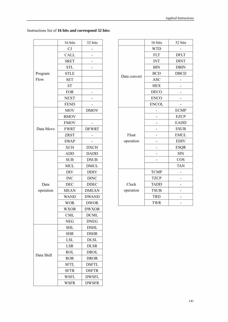
Applied Instructions
Instructions list of 16 bits and correspond 32 bits:
16 bits 32 bits WTD - FLT DFLT INT DINT BIN DBIN BCD DBCD ASC - HEX -
DECO - ENCO -
Data convert
ENCOL - - ECMP - EZCP - EADD - ESUB - EMUL - EDIV - ESQR - SIN - COS
Float operation
TAN TCMP - TZCP - TADD - TSUB - TRD -
Clock operation
TWR -
16 bits 32 bits CJ -
CALL - SRET - STL -
STLE SET ST
FOR - NEXT -
Program Flow
FEND - MOV DMOV
BMOV FMOV - FWRT DFWRT ZRST - SWAP -
Data Move
XCH DXCH ADD DADD SUB DSUB MUL DMUL DIV DDIV INC DINC DEC DDEC
MEAN DMEAN WAND DWAND WOR DWOR
WXOR DWXOR CML DCML
Data operation
NEG DNEG SHL DSHL SHR DSHR LSL DLSL LSR DLSR ROL DROL ROR DROR SFTL DSFTL SFTR DSFTR WSFL DWSFL
Data Shift
WSFR DWSFR
141
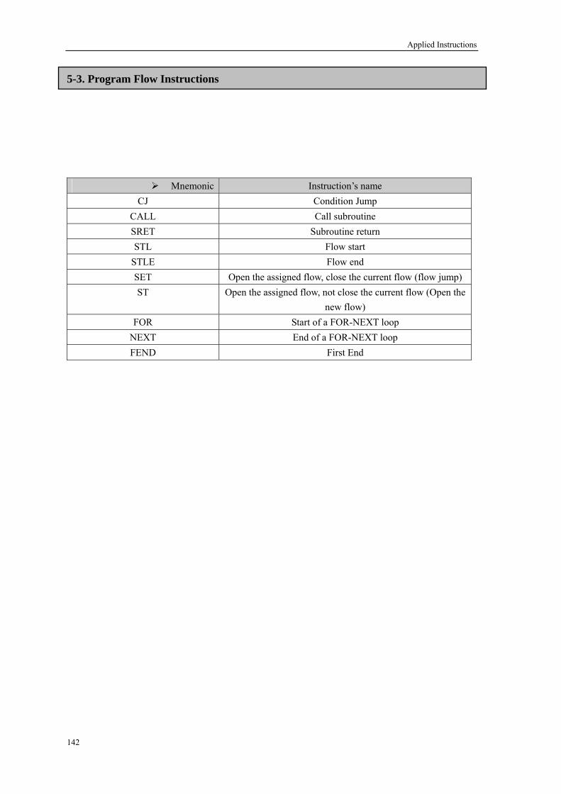
Applied Instructions
142
5-3. Program Flow Instructions
Mnemonic Instruction’s name CJ Condition Jump
CALL Call subroutine SRET Subroutine return STL Flow start
STLE Flow end SET Open the assigned flow, close the current flow (flow jump) ST Open the assigned flow, not close the current flow (Open the
new flow) FOR Start of a FOR-NEXT loop
NEXT End of a FOR-NEXT loop FEND First End
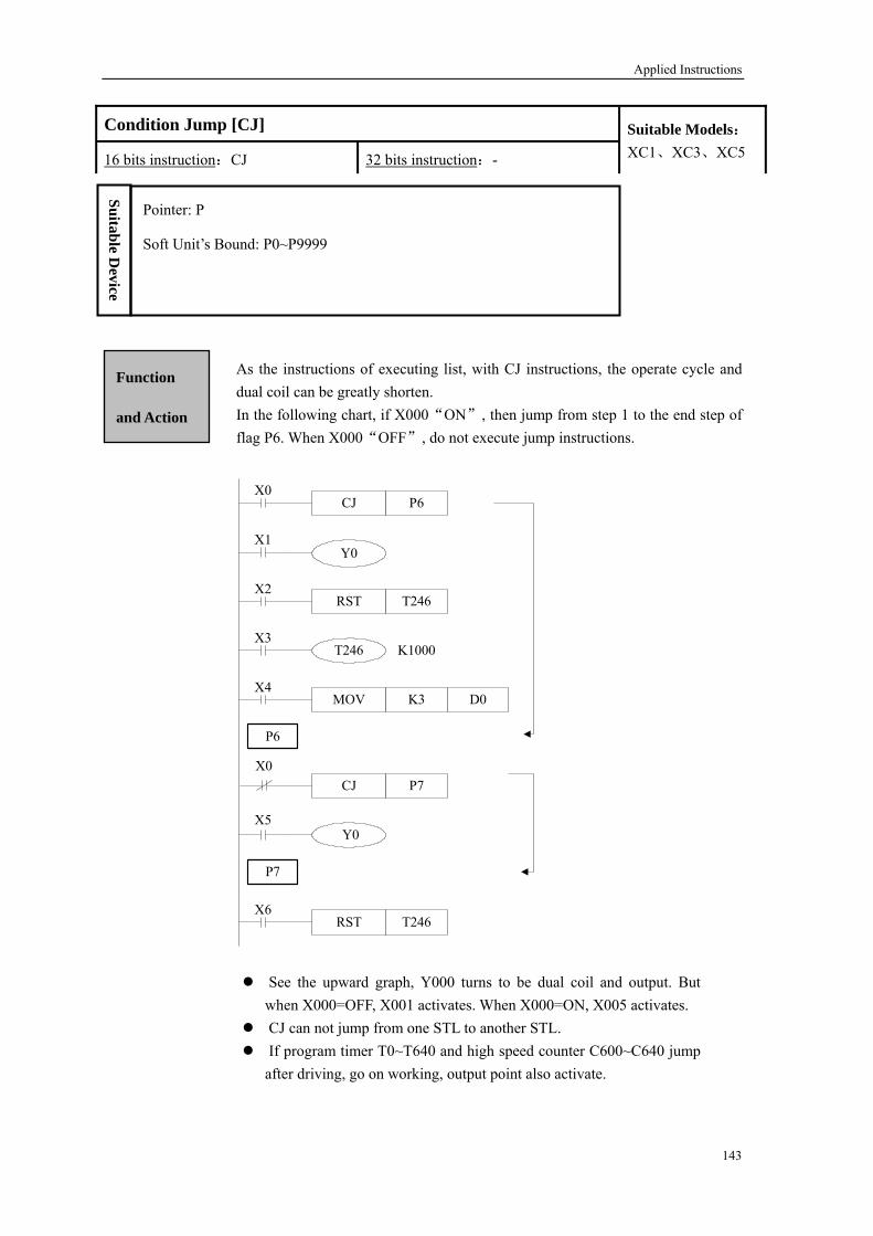
Applied Instructions
As the instructions of executing list, with CJ instructions, the operate cycle and dual coil can be greatly shorten. In the following chart, if X000“ON”, then jump from step 1 to the end step of flag P6. When X000“OFF”, do not execute jump instructions.
CJ
Y0
X0
X1
X3
X4
X0
RST
T246 K1000
MOV
CJ
X2
X5
X6
P6
T246
K3 D0
P7
T246RST
Y0
P6
P7
See the upward graph, Y000 turns to be dual coil and output. But when X000=OFF, X001 activates. When X000=ON, X005 activates.
CJ can not jump from one STL to another STL. If program timer T0~T640 and high speed counter C600~C640 jump
after driving, go on working, output point also activate.
Condition Jump [CJ]
16 bits instruction:CJ 32 bits instruction:-
Suitable Models: XC1、XC3、XC5
Pointer: P
Soft Unit’s Bound: P0~P9999
Suitable Device
Function
and Action
143

Applied Instructions
CALLX0
FEND
SRET
END
P10
P10
Call subroutine [CALL] and Subroutine return [SRET]
16 bits instruction:CALL、SRET 32 bits instruction:-
Suitable Models: XC1、XC3、XC5
Pointer: P
Soft Unit’s Bound: P0~P9999
Suitable Device
Function
If X000“ON”, carry on Jump instruction and jump to step of flag P10. Here, after executing the subroutine, return to the original step via executing SRET instruction. After the following FEND instruction, program with the flag.
In the subroutine, 9 levels Call instruction is allowed, so to the all, 10 levels nesting is available.
Main program
Subroutine
144
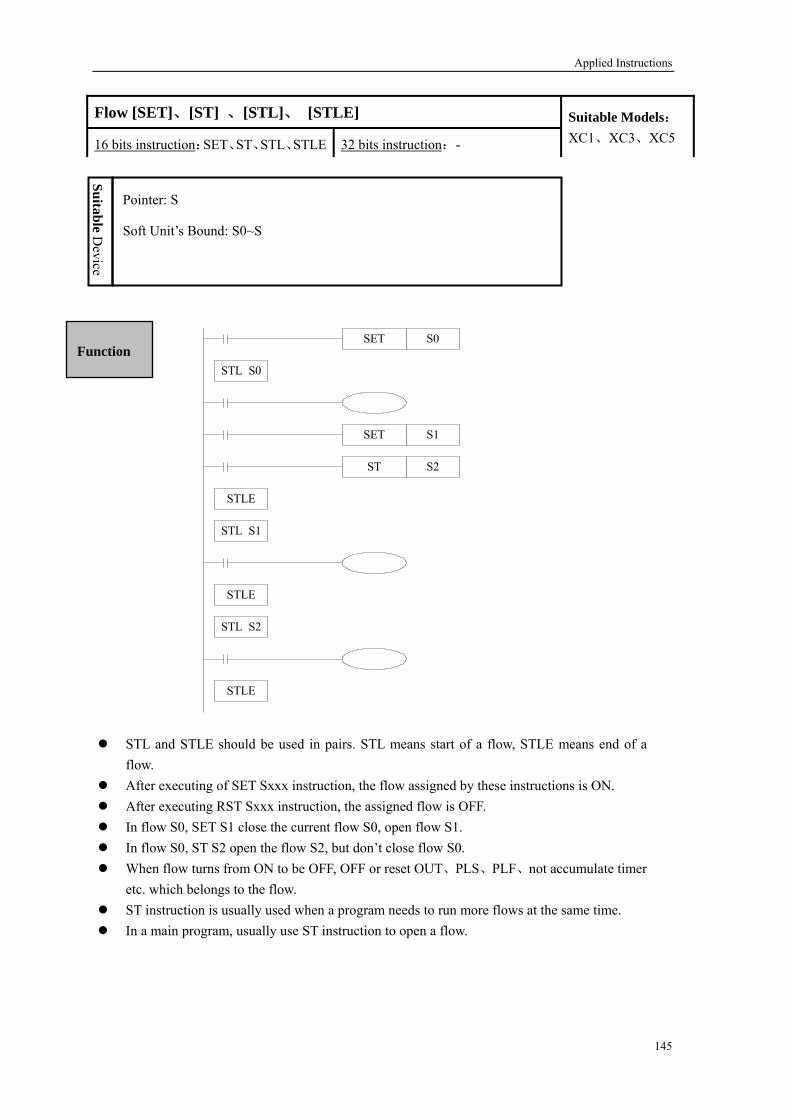
Applied Instructions
SET S0
STL S0
SET S1
ST S2
STL S1
STLE
STLE
STL S2
STLE
STL and STLE should be used in pairs. STL means start of a flow, STLE means end of a flow.
After executing of SET Sxxx instruction, the flow assigned by these instructions is ON. After executing RST Sxxx instruction, the assigned flow is OFF. In flow S0, SET S1 close the current flow S0, open flow S1. In flow S0, ST S2 open the flow S2, but don’t close flow S0. When flow turns from ON to be OFF, OFF or reset OUT、PLS、PLF、not accumulate timer
etc. which belongs to the flow struction is usually used when a program needs to run more flows at the same time. In a main program, usually use ST instruction to open a flow.
Flow [SET]、[S ]、 [STLE] T] 、[STL
16 bits instruction:SET、ST、STL、STLE 32 bits instruction:-
Suitable Models: XC1、XC3、XC5
Pointer: S
Soft Unit’s Bound: S0~S
Suitable Device
Function
. ST in
145
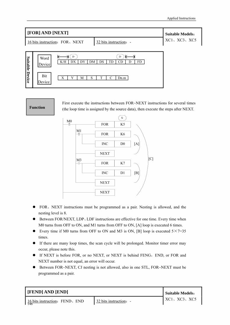
Applied Instructions
First execute the instructions between FOR~NEXT instructions for several times (the loop time is assigned by the source data), then execute the steps after NEXT.
FOR K6
INC D0
NEXT
FOR K7
INC D1
NEXT
NEXT
FOR K5M0
M3
M1
[A]
[B]
[C]
S·
FOR、NEXT instructions must be programmed as a pair. Nesting is allowed, and the nesting level is 8.
Between FOR/NEXT, LDP、LDF instructions are effective for one time. Every time when M0 turns from OFF to ON, and M1 turns from OFF to ON, [A] loop is executed 6 times.
Every time if M0 turns from OFF to ON and M3 is ON, [B] loop is executed 5×7=35 times.
If there are many loop times, the scan cycle will be prolonged. Monitor timer error may occur, please note this.
If NEXT is before FOR, or no NEXT, or NEXT is behind FENG,END, or FOR and NEXT number is not equal, an error will occur.
Between FOR~NEXT, CJ nesting is not allowed, also in one STL, FOR~NEXT must be programmed as a pair.
[FOR] AND [NEXT]
16 uction bits instr :FOR、NEXT 32 bits instruction:- XC1、XC3Suitable Models:
、XC5
[FEND] AND [END]
16 bits instruction:FEND、END 32 bits instruction:-
Suitable Models: XC1、XC3、XC5
Suitable Device
Word Device
Bit ce Devi
X Y M S T C Dn.m
D FDDMDX DY DS TD CDK/HD· D·
Function
146
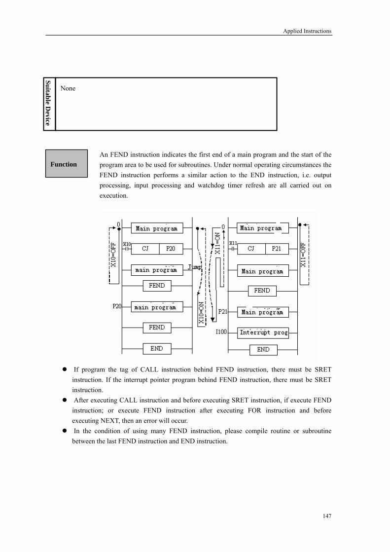
Applied Instructions
An FEND instru he first end of a m and the start of the program area to be used for subroutines. Under normal operating circumstances the FEND instruction performs a similar action to the END instruction, i.e. output processing, inpu and watchdog timer refresh are all carried out on execution.
ction indicates t ain program
t processing
N
Su
one itable Device
Function
If program the tag of CALL instruction behind FEND instruction, there must be SRET
instruction. If the interrupt pointer program behind FEND instruction, there must be SRET instruction.
After executing CALL instruction and before executing SRET instruction, if execute FEND instruction; or execute FEND instruction after executing FOR instruction and before executing NEXT, then an error will occur.
In the condition of using many FEND instruction, please compile routine or subroutine between the last FEND instruction and END instruction.
147

Applied Instructions
5-4. Contactor’s Compare Instructions
monic Function
Mnemonic & Function
Mne
LD= Initial comparison contact. Active when the comparison (S1)= . (S2) is trueLD> Initial comparison contact. Active when the comparison (S1)> (S2) is true LD< parison contact. Active when the comparison (S1)< (S2) is true Initial com
LD<> Initial comparison contact. Active when the comparison (S1)≠(S2) is true LD<= Initial comparison contact the comparison (S1)≤(S2) is true . Active whenLD>= Initial comparison contact. Active when the comparison (S1)≥(S2) is true AND= omparison contact the comparison (S1)=(S2)is true. Serial c . Active whenAND> Serial comparison contact. Active when the comparison (S1)> (S2) is true. AND< Serial comparison contact. Active when the comparison (S1)< (S2) is true.
AND<> Serial comparison contact. Active when the comparison (S1)≠(S2) is true. AND<= Serial comparison contact. Active when the comparison (S1)≤(S2) is true. AND>= Serial comparison contact. Active when the comparison (S1)≥(S2) is true.
OR= Parallel comparison contact. Active when the comparison (S1)=(S2) is true. OR> Parallel comparison contact. Active when the comparison (S1)> (S2) is true. OR< Parallel comparison contact. Active when the comparison (S1)< (S2) is true.
OR<> Parallel comparison contact. Active when the comparison (S1)≠(S2) is true. OR<= Parallel comparison contact. Active when the comparison (S1)≤(S2) is true. OR>= Parallel comparison contact. Active when the comparison (S1)≥(S2) is true.
148

Applied Instructions
n. If the comparison is true then the LD contact is active. If the comparison is false then the LD contact is not active. 16 bits
32 bits
Active t
ion
Inactive condition
The value of S1 and S2 are tested according to the comparison of the instructio
condi
LD DL=
D= (S1)=(S2) (S1)≠(S2)
LD DLD> ) (S1)≤(S2) >
(S1)>(S2
LD
DLD< (S1)<(S2) (S1)≥(S2) <
LD
DLD<> (S1)≠(S2) (S1)=(S2) <
>
LD<
=
DLD<= (S1)≤(S2) (S1)>(S2)
LD>
=
DLD>= (S1)≥(S2) (S1)<(S2)
LD> D200 K-30 SET Y1
DLD> K68899 C300 M50
X0
M4
S1· S2·
LD= K100 C0 Y0X0
Instruction & Function
Program
Initial Comparison LD
16 bits instruction:Refer Below 32 bits instruction:Refer Below
Suitable Models: XC1、XC3、XC5
Word Device
Bit Device
X Y M S T C Dn.m
D FDDMDX DY DSS1· S2·
TD CDK/H
149

Applied Instructions
The value of S1 and S2 are tested according to the comparison of the instruction. If the comparison is true then the LD contact is active. If the comparison is false then the LD contact is not active.
16 bits
32 bits
Active condition
Inactive condition
When the source data’s highest bit (16 bits:b15,32 bits:b31) is 1,
st use 32 bits instruction. If assigned as 16 bits instruct ll lead the program error or operation error.
use the data as a negative. The comparison of 32 bits counter (C300~) mu
ion, it wi
AND=
DAND= (S1)=(S2) (S1)≠(S2)
AND>
DAND> (S1)>(S2) (S1)≤(S2)
AND<
DAND< (S1)<(S2) (S1)≥(S2)
AND<>
DAND<> (S1)≠(S2) (S1)=(S2)
AND<=
DAND<= (S1)≤(S2) (S1)>(S2)
AND>=
DAND>= (S1)≥(S2) (S1)<(S2)
Note Items
Instruction & Function
Program
Serial AND Refer Below
1 struction6 bits in :Ref 32 bits instructioner Below :Refer Below
Suitable Models: XC1、XC3、XC5
Word Device
Bit Device
X Y M S T C Dn.m
D FDDMDX DY DSS1· S2·
TD CDK/H
150

Applied Instructions
151
AND= K100 C0 Y0
AND> D0K-30 SET Y1
DAND> K68899 D10 M50
X1
M4
X0
X2
S1· S2·
Note Items
operation error.
When the source data’s highest bit (16 bits:b15,32 bits:b31) is 1,use the data as a negative.
The comparison of 32 bits counter (C300~) must use 32 bits instruction. If assigned as 16 bits instruction, it will lead the program error or
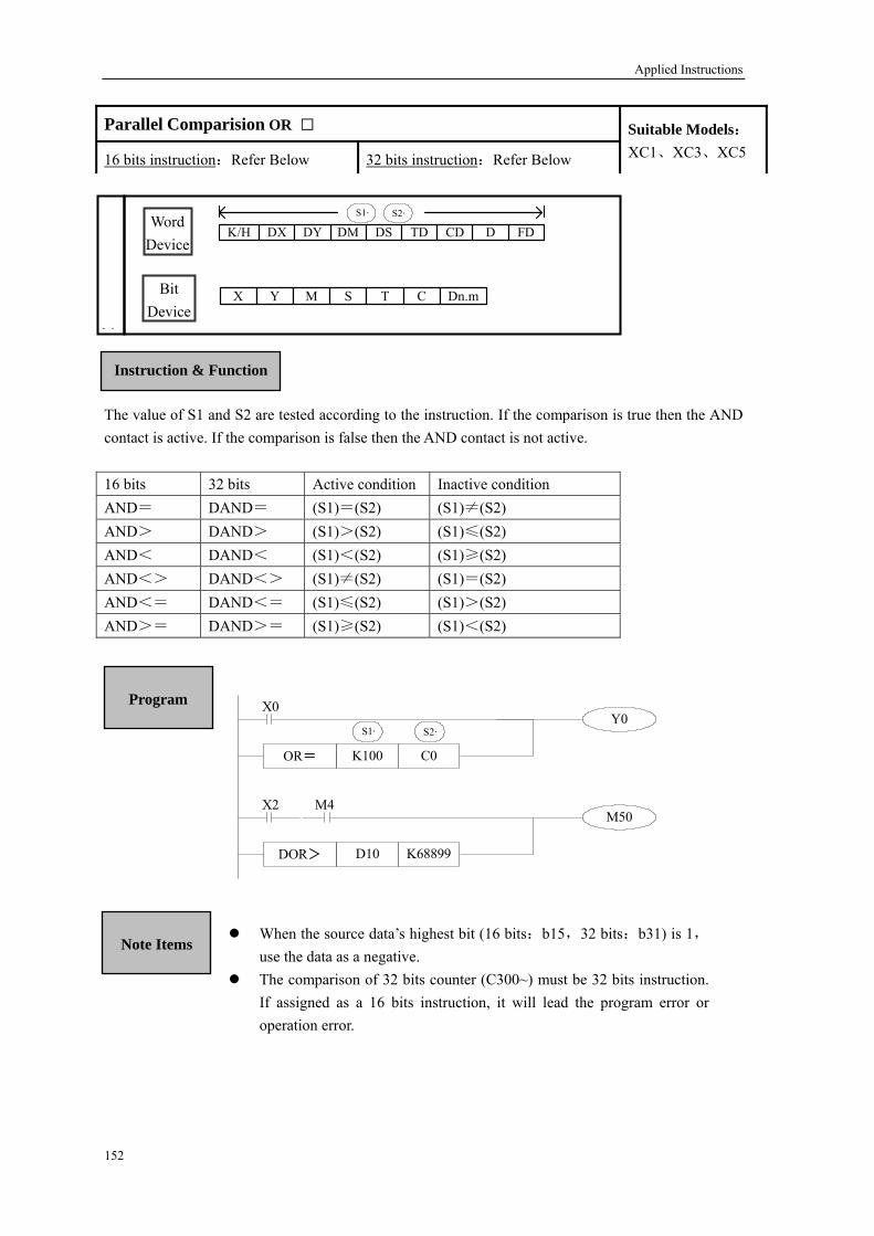
Applied Instructions
The tested according to the instruction. If the comparison is true then the AND contact is active. If the comparison is false then the AND contact is not active. 16 bits 32 bits Active condition Inactive condition
value of S1 and S2 are
AND= DAND= (S1)=(S2) (S1)≠(S2) AND> DAND> (S1)>(S2) (S1)≤(S2) AND< DAND< (S1)<(S2) (S1)≥(S2) AND 2) (S1)=(S2) <> DAND<> (S1)≠(SAND<= DAND<= (S1)≤(S2) (S1)>(S2) AND>= DAND>= (S1)≥(S2) (S1)<(S2)
OR= K100 C0
Y0
DOR> K68899D10
M50M4
X0
X2
S1· S2·
Instruction & Function
Program
When the source data’s highest bit (16 bits:b15,32 bits:b31) is 1,use the data as a negative.
The comparison of 32 bits counter (C300~) must be 32 bits instruction. If assigned as a 16 bits instruction, it will lead the program error or operation error.
Note Items
Parallel Comparision OR
16 bits instruction:Refer Below 32 bits instruction:Refer Below
Suitable Models: XC1、XC3、XC5
D FDDMDX DY DS
S1· S2·
TD CDK/H
Word Device
Bit Device
X Y M S T C Dn.m
152
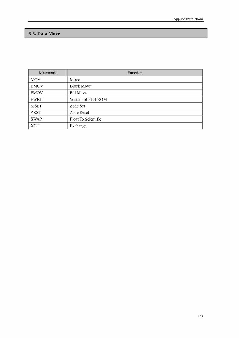
Applied Instructions
153
5-5. Data Move
Mnemonic Function MOV Move BMOV Block Move FMOV Fill Move FWRT Written of FlashROM MSET Zone Set ZRST Zone Reset SWAP Float To Scientific XCH Exchange

Applied Instructions
X0K10 D10MOV
S· D·
《Read out the current value of timer, counter》
MOV T0 D20X1
《Indirect assign the set value of timer, counter》
MOV K10 D20X2
M0T20 D20
《Move of 32 bits data》
DMOV D0 D10
DMOV C235 D20
Function & Action
Move data from one storage area to a new one.
(K10)(D10)
D20=K10
(T0 current value)→(D20)
It’s the same with the counter.
(D1,D0)→(D11,D10)
(C235, current value)→(D21,D20)
Move contents from source to destination If X000 is OFF, data will not change. Constant K10 will automatically convert to be BIN code.
[MOV]
16 bits instruction:MOV 32 bits instruction:DMOV
Suitable Models: XC1、XC3、XC5
Suitable Device
Word Device
Bit Device
X Y M S T C Dn.m
D·
S·
D FDDMDX DY DS TD CDK/H
154

Applied Instructions
A quantity of consecutively occurring data elements can be copied to a new destination. The
source data is identified as a device head address(S) and a quantity of consecutive data elements (n). This is moved to the destination device (D) for the same number of elements (n). (If the quantity of source device (n) exceeds the actual number of available source devices, then only those devices which fall in the available range will be used. If the number of source devices exceeds the available space at the destination location, then only the available destination devices will be written to.)
BMOV D5 D10 K3X0
nS· D·
D5
D6
D7
D10
D11
D12
n=3
The BMOV instruction has a built in automatic feature to prevent overwriting errors from
occurring when the source (S-n) and destination (D-n) data ranges coincide. This is clearly identified in the following diagram:
(NOTE: The numbered arrows indicate the order in which the BMOV is processed).
D10
D11
D12
D9
D10
D11
D10
D11
D12
D11
D12
D13
①
②
③
③
②
①
Function
[BMOV]
16 bits instruction:BMOV 32bits instruction:-
Suitable Models: XC1、XC3、XC5
Suitable Device
Word Device
Bit Device
S·
nD FDDMDX DY DS TD CDK/H
D·
X Y M S T C Dn.m
155

Applied Instructions
FMOV K0 D0 K10X0
nS· D·
Function
[FMOV]
16 bits instruction:FMOV 32 bits instruction:-
Suitable Models: XC1、XC3、XC5
Suitable Device
Word Device
Bit Device
S·
D FDDMDX DY DS TD CDK/Hn D·
X Y M S T C Dn.m
Move K0 to D0~D9. Copy a single data device to a range of destination devices. The data stored in the source device (S) is copied to every device within the destination range,
The range is specified by a device head address (D) and a quantity of consecutive elements (n). If the specified number of destination devices (n) exceeds the available space at the destination
location, then only the available destination devices will be written to.
K0 D0K0
n
D1K0
D2K0
D3K0
D4K0
D5K0
D6K0
D7K0
D8K0
D9K0
156
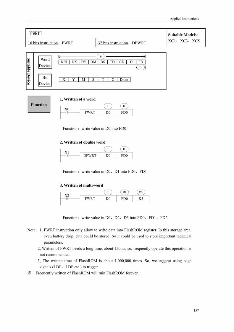
Applied Instructions
1, Written of a word
D0FWRT FD0X0
S· D·
2, Written of double word
D0DFWRT FD0X1
S· D·
3, Written of multi-word
D0FWRT FD0X2
K3
S· D1· D3·
Note:1, FWRT instruction only allow to write data into FlashROM register. In this storage area, even battery drop, data could be stored. So it could be used to store important technical parameters.
2, Written of FWRT needs a long time, about 150ms, so, frequently operate this operation is not recommended.
3, The written time of FlashROM is about 1,000,000 times. So, we suggest using edge signals (LDP、LDF etc.) to trigger.
※ Frequently written of FlashROM will ruin FlashROM forever.
[FWRT]
16 bits instruction:FWRT 32 bits instruction:DFWRT
Suitable Models: XC1、XC3、XC5
Suitable Device
Word Device
Bit
D·
S·
D FDDMDX DY DS TD CDK/H
X Y M S T C Dn.mDevice
Function:write value in D0 into FD0
Function:write value in D0、D1 into FD0、FD1
Function:write value in D0、D2、D3 into FD0、FD1、FD2.
Function
157
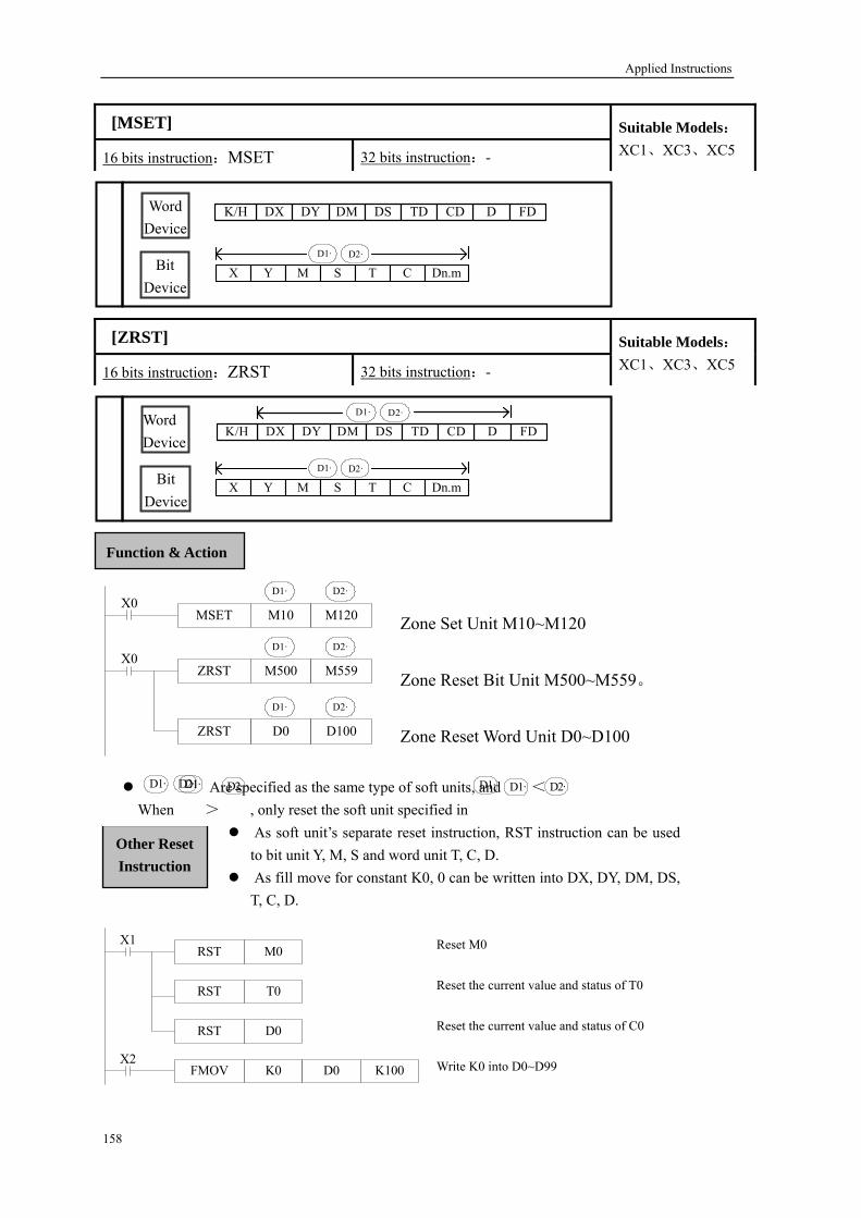
Applied Instructions
ZRST M500 M559
D0 D100
D1· D2·
D1· D2·
X0
ZRST
MSET M10 M120
D1· D2·X0
X1RST M0
RST T0
RST D0
X2K0FMOV D0 K100
Function & Action
Zone Set Unit M10~M120
Zone Reset Bit Unit M500~M559。
Zone Reset Word Unit D0~D100
Other Reset Instruction
Reset M0
Reset the current value and status of T0
Reset the current value and status of C0
Write K0 into D0~D99
As soft unit’s separate reset instruction, RST instruction can be used to bit unit Y, M, S and word unit T, C, D.
As fill move for constant K0, 0 can be written into DX, DY, DM, DS, T, C, D.
Are specified as the same type of soft units, and < When > , only reset the soft unit specified in
D1· D2·D1· D1· D1·D2· D2·
[MSET]
16 bits instruction:MSET 32 bits instruction:-
Suitable Models: XC1、XC3、XC5
Word
D1· D2·
D FDDMDX DY DS TD CDK/HDevice
Bit X Y M S T C Dn.mDevice
[ZRST]
16 bits in onstructi :ZRST 32 bits instruction:-
Suitable Models: XC1、XC3、XC5
WD
ord evice
Bit Device
X Y M S T CD1· D2·
D FDDMDX DY DS TD CDK/HD1· D2·
Dn.m
158

Applied Instructions
D10
High 8 bits Low 8 bits
Function
Low 8 bits and high 8 bits change when it is 16 bits instruction. If the instruction is a consecutive executing instruction, each operation cycle should change.
[SWAP]
16bits instruction:SWAP 32 bits instruction:-
Suitable Models: XC1、XC3、XC5
Suitable Device
Word Device
Bit Device
D FDDMDX DY DS TD CDK/HS·
X Y M S T C Dn.m
159

Applied Instructions
《16 bits instruction》
XCH D10 D11X0
D1· D2·
《32 bits instruction》
DXCH D10 D20X0
D1· D2·
Function
[XCH]
16 bits instruction:XCH 32 bits instruction:DXCH
Suitable Models: XC1、XC3、XC5
The contents of the two destination devices D1 and D2 are swapped,
When drive input X0 is ON each scan cycle should carry on data exchange
Before(D10)=100 →After (D10)=101
(D11)=101 (D11)=100
32 bits instruction [DXCH] swaps value composed by D10、D11 and the value
composed by D20 D21
Suitable Device
Word Device
Bit Device
X Y M S T C Dn.m
D FDDMDX DY DS TD CDK/HD1· D2·
160

Applied Instructions
5-6. Data Operation Instructions
Mnemonic Function ADD Addition SUB Subtraction MUL Multiplication DIV Division INC Increment DEC Decrement
MEAN Mean WAND Logic Word And WOR Logic Word Or
WXOR Logic Exclusive Or CML Compliment NEG Negation
161
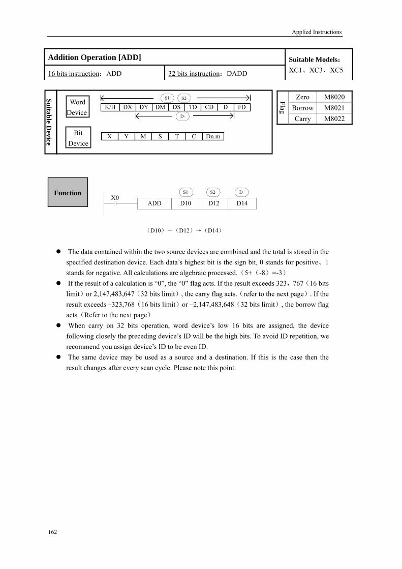
Applied Instructions
ADD D10 D12 D14X0
S1· S2· D·
Function
The data contained within the two source devices are combined and the total is stored in the specified destination device. Each data’s highest bit is the sign bit, 0 stands for positive、1 stands for ne gebraic processed.(5+(-8)=-3)
If the result of a calculation is “0”, the “0” flag acts. If the result exceeds 323,767(16 bits limit)or 2,147,483,647(32 bits limit), the carry flag acts.(refer to the next page). If the result exceeds –323,768(16 bits limit)or –2,147,483,648(32 bits limit), the borrow flag acts(Refer to the next page)
When carry on 32 bits operation, word device’s low 16 bits are assigned, the device following cl ely the preceding device’s ID will be the high bits. To avoid ID repetition, we recommend u assign device’s ID to be even ID.
The same device may be used as a source and a destination. If this is the case then the result changes after every scan cycle. Please note this point.
(D10)+(D12)→(D14)
Addition Operation [ADD]
16 bits instruction:ADD 32 bits instruction:DADD
Suitable Models: XC1、XC3、XC5
Zero M8020 Borrow M8021
Flag Carry M8022
Suitable Device
Word Device
Bit Device
X Y M S T C Dn.m
D FDDMDX DY DS TD CDK/HS1· S2·
D·
gative. All calculations are al
osyo
162

Applied Instructions
SUB D10 D12 D14
X0S1· S2· D·
The relationship of the flag’s action and vale’s positive/negative is shown below:
Function
(D10)—(D12)→(D14)
appoint the soft unit’s content, subtract the soft unit’s content appointed by in the format of algebra. The result will be stored in the soft unit appointed by . (5-(-8)=13)
The action of each flag, the appointment method of 32 bits operation’s soft units are both the same with the preceding ADD instruction.
The importance is: in the preceding program, if X0 is ON, SUB operation will be executed every scan cycle
S1· S2·
D·
UB] [S
16 bits instruction:SUB 32 bits instruction:DSUB
Suitable Models: XC1、XC3、XC5
Zero M8020Borrow M8021
Flag Carry M8022
Suitable Device
Word Device
Bit Device
X Y M S T C Dn.m
D FDDMDX DY DS TD CDK/HS1· S2·
D·
163

Applied Instructions
《16 bits operation》
MUL D0 D2 D4X0
S1· S2· D·
《32 bits operation》
X1DMUL D0 D2 D4
S1· S2· D·
Function & action
BIN BIN BIN
(D0) × (D2) → (D5, D4)
16 bits 16 bits → 32 bits
BIN BIN BIN
(D1,D0) × (D3,D2) → (D7,D6,D5,D4)
32 bits 32 bits → 64 bits
The contents of the two source devices are multiplied together and th is stored at the destination device in the format of 32 bits. As in the upward chart: when (D0)=8、(D2)=9, (D5, D4) =72.
The result’s highest bit is the symbol bit: positive (0)、negative (1). When be bit unit, it can carry on the bit appointment of K1~K8. When appoint K4, only
the result’s low 16 bits can be obtained.
e result
In 32 bits operation, when use bit device as the destination address, only low 32 bits result can be obtained. The high 32 bits result can not be obtained, so please operate again after transfer one time to the word device
Even use word device, 64 bits results can’t be monitored at once. In this situation, float point data operation is recommended.
[MUL]
16 bits instruction:MUL 32 bits instruction:DMUL
Suitable Models: XC1、XC3、XC5
Zero M8020Borrow M8021
Flag Carry M8022
Word Device
Bit Device
D FDDMDX DY DS TD CDK/HS1· S2·
D·
X Y M S T C Dn.m
164
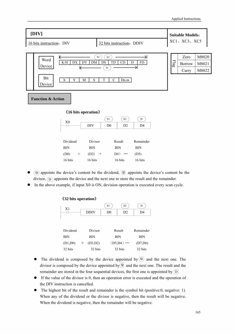
Applied Instructions
《16 bits operation》
DIV D0 D2 D4X0
S1· S2· D·
《32 bits operation》
DDIV D0 D2 D4X1
S1· S2· D·
DDIV D0 D2 D4X1
S1· S2· D·
Function & Action
Dividend Divisor Result Remainder
BIN BIN BIN BIN
(D0) ÷ (D2) → D4) (D5)
16 bits 16 bits 16 bits 16 bits
Dividend Divisor Result Remainder
BIN BIN BIN BIN
(D1,D0) ÷ (D3,D2) (D5,D4) (D7,D6)
32 bits 32 bits 32 bits 32 bits
appoints the device’s content be the dividend, appoints the device’s content be the divisor, appoints the device and the next one to store the result and the remainder.
In the above example, if input X0 is ON, devision operation is executed every scan cycle.
S1· S2·
D·
The dividend is composed by the device appointed by and the next one. The divisor is composed by the device appointed by and the next one. The result and the remainder are stored in the four sequential devices, the first one is appointed by
If the value of the divisor is 0, then an operation error is executed and the operation of the DIV instruction is cancelled.
The highest bit of the result and remainder is the symbol bit (positive:0, negative: 1). When any of the dividend or the divisor is negative, then the result will be negative. When the dividend is negative, then the remainder will be negative.
S1·
S2·
D·
[DIV]
16 bits instruction:DIV 32 bits instruction:DDIV
Suitable Models: XC1、XC3、XC5
Zero M8020Borrow M8021
Flag Carry M8022
Word Device
Bit Device
X Y M S T C Dn.m
D FDDMDX DY DS TD CDK/HS1· S2·
D·
165

Applied Instructions
166
INC D0X0
D·
DEC D0
X1D·
Function & Action
(D0)+1→(D0)
(D0)-1→(D0)
On every execution of the instruction the device specified as the destination has its current valu incremented (increased) by a value of 1.
In 16 bits operation, when +32,767 is reached, the next increment will write -32,767 to the destination device. In this case, there’s no additional flag to identify this change in the
nted value.
e
cou
D·
On every execution of the instruction the device specified as the destination has its current value decremented (decreased) by a value of 1.
When -32,768 or -2,147,483,648 is reached, the next decrement will write +32,767 or +2,147,483,647 to the destination device.
D·
1、Increment [INC]
2、Decrement [DEC]
[INC] & [DEC]
16 bits instruction:INC、DEC 32 bits instruction:DINC、DDEC
Suitable Models: XC1、XC3、XC5
Zero M8020Borrow M8021
Flag Carry M8022
Word Device
Bit Device
D FDDMDX DY DS TD CDK/HD·
X Y M S T C Dn.m

Applied Instructions
MEAN D0 D10 K3
S· D·X0
n
(D0) + +
3(D10)
(D1) (D2)
Function & Action
The value of all the devices within the source range is summed and then divided by the number of devices summed, i.e. n.. This generates an integer mean value which is stored in the destination device (D) The remainder of the calculated mean is ignored.
If the value of n is specified outside the stated range (1 to 64) an error is generated.
[MEAN]
16 bits instruction:MEAN 32 bits instruction:-
Suitable Models: XC1、XC3、XC5
Zero M8020Borrow M8021
Flag Carry M8022
Word Device
Bit Device
S·
nD FDDMDX DY DS TD CDK/H
D·
X Y M S T C Dn.m
167

Applied Instructions
[WAND]、 [WOR] &
Execute logic AND operation with each bit
WAND D10 D12 D14
D·X0
S1· S2·
Execute logic OR operation with each bit
WOR D10 D12 D14
D·X0
S1· S2·
Execute logic Exclusive OR operation with each bit.
WXOR D10 D12 D14
D·X0
S1· S2·
If use this instruction along with CML instruction, XOR NOT operation could also be executed.
0&0=0 0&1=0 1&0=0 1&1=1
0 or 0=0 0 or 1=1 1 or 0=1 1 or 1=1
0 xor 0=0 0 xor 1=1 1 xor 0=1 1 xor 1=0
[WXOR]
16 bits instruction:WAND、WOR 32 bits instruction:DWAND、DWOR
Suitable Models: XC1、XC3、XC5
Zero M8020Borrow M8021
Flag Carry M8022
Word D FDDMDX DY DS TD CDK/H
S1· S2·
Device D·
Bit X Y M S T C Dn.mDevice
WXOR D10 D12 D14
D·X0
S1· S2·
CML D14 D14
Functio ction n & A
168

Applied Instructions
CML D0 DY0
S· D·X0
A copy of each data bit within the source device is inverted and then moved to the designated destination.
《Reading of inverted input》
M0
M1
M2
M3
M17
CML DX0 DM0M8000
X0
X1
X2
X3
X17
Function & Action
The sequential control instruction ithe left could be denoted by following CML instruction.
n the
Each data bit in the source device is inverted (0->1, 1->0) and sent to the destination device. If use constant K in the source device, it can be auto convert to be binary.
It’s available when you want to inverted output the PLC’s output
[CML]
16 bits instruction:CML 32 bits instruction:DCML
Suitable Models: XC1、XC3、XC5
Word Device
Bit Device
D·
S·
D FDDMDX DY DS TD CDK/H
X Y M S T C Dn.m
169
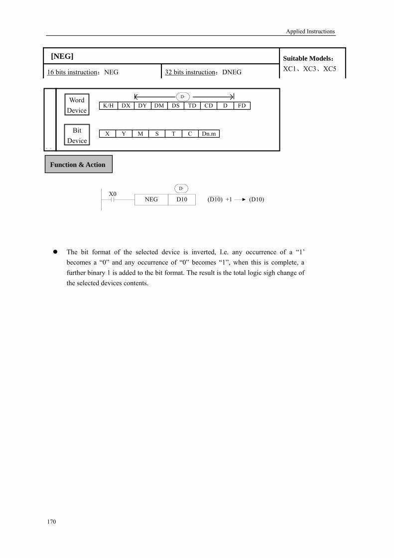
Applied Instructions
170
NEG D10 (D10) +1 (D10)X0
D·
Function & Action
The bit format of the selected device is inverted, I.e. any occurrence of a “1’ becomes a “0” and any occurrence of “0” becomes “1”, when this is complete, a further binary 1 is added to the bit format. The result is the total logic sigh change of the selected devices contents.
[NEG]
16 bits instruction:NEG 32 bits instruction:DNEG
Suitable Models: XC1、XC3、XC5
Word Device
Bit Device
X Y M S T C Dn.m
D FDDMDX DY DS TD CDK/HD·
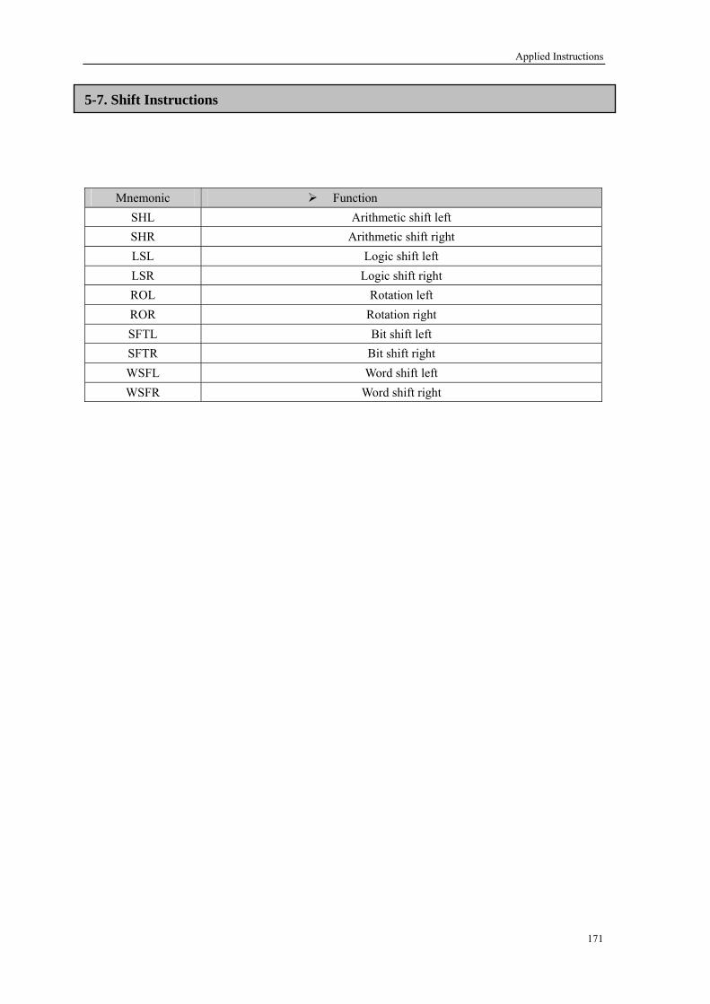
Applied Instructions
171
5-7. Shift Instructions
Mnemonic Function SHL Arithmetic shift left SHR Arithmetic shift right LSL Logic sh leftift LSR Logic shift right ROL Rotation left ROR Rotation right SFTL Bit shift left SFTR Bit shift right WSFL Word shift left WSFR Word shift right

Applied Instructions
172
t left》
《Arithmetic shif
《Arithmetic shift right》
Function &
Action
After once execution, the high bit is same with the bit before shifting, the final bit is stored in carry flag.
After once execution, the low bit is filled in 0, the final bit is stored in carry flag.
[SHL] & [SHR]
16 bits instruction:SHL、SHR 32 bits instruction:DSHL、DSHR
Suitable Models: XC3、XC5
Note: In the left example, when X1 is ON, left/right shift is executed at every scan cycle.
Word Device
Bit Device
X Y M S T C Dn.m
D FDDMDX DY DS TD CDK/HD·n
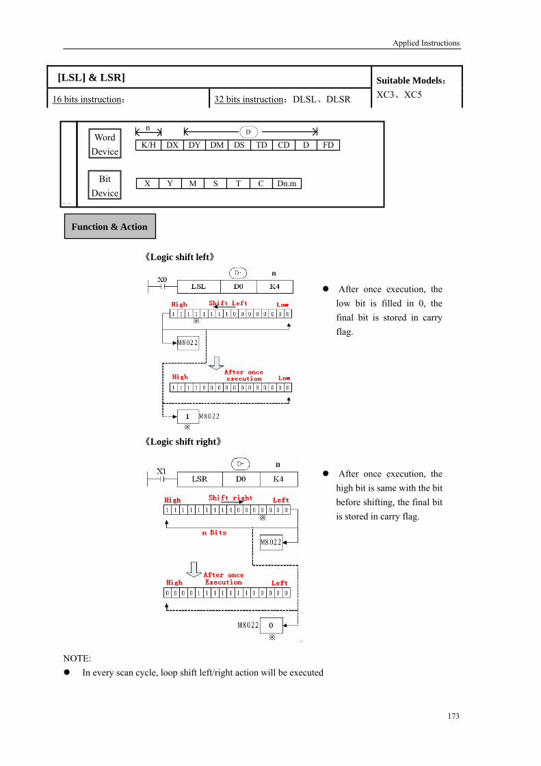
Applied Instructions
《Logic shift le
ft》
《Logic shift right》
Function & Action
After oncit is
e execution, the filled in 0, the
t is stored in carry flag.
low bfinal bi
After once execution, the high bit is same with the bit before shifting, the final bit is stored in carry flag.
NOTE: In every scan cycle, loop shift left/right action will be executed
[LSL] & LSR]
16 bits instruction: 32 bits instruction:DLSL、DLSR
Suitable Models: XC3、XC5
Word Device
Bit Device
D FDDMDX DY DS TD CDK/HD·n
X Y M S T C Dn.m
173

Applied Instructions
The bit format of the destination device is rotated n bit places to the left on every operation of the instruction
《Rotation shift left》
《Rotation shift right》
Function & Action
Every time when X000 turns from OFF to ON, executes n bits left rotation.
Every time when X000 turns from OFF to ON, executes n bits right rotation.
[ROL] & [ROR]
16 bits instruction:ROL、ROR 32 bits instruction:DROL、DROR
Suitable Models: XC3、XC5
Word Device
Bit Device
D FDDMDX DY DS TD CDK/HD·n
X Y M S T C Dn.m
174
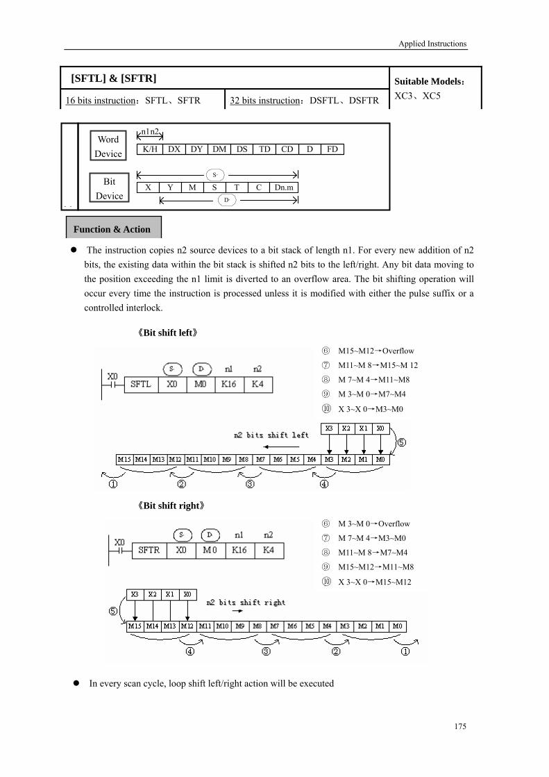
Applied Instructions
《Bit shift left》
《Bit shift right》
Function & Action
⑥ M15~M12→Overflow
⑦ M11~M 8→M15~M 12
⑧ M 7~M 4→M11~M8
⑨ M 3~M 0→M7~M4
⑩ X 3~X 0→M3~M0
⑥ M 3~M 0→Overflow
⑦ M 7~M 4→M3~M0
⑧ M11~M 8→M7~M4
⑨ M15~M12→M11~M8
⑩ X 3~X 0→M15~M12
In every scan cycle, loop shift left/right action will be executed
[SFTL] & [SFTR]
16 bits instruction:SFTL、SFTR 32 bits instruction:DSFTL、DSFTR
Suitable Models: XC3、XC5
n1n2
Word Device D FDDMDX DY DS TD CDK/H
Bit Device
X Y M S T C Dn.mD·
S·
The instruction copies n2 source devices to a bit stack of length n1. For every new addition of n2 bits, the existing ta within the bit stack is shifted n2 bits to the left/right. Any bit data moving to the position exceeding the n1 limit is diverted to an overflow area. The bit shifting operation will occur every time the instruction is processed unless it is modified with either the pulse suffix or a controlled interlock.
da
175
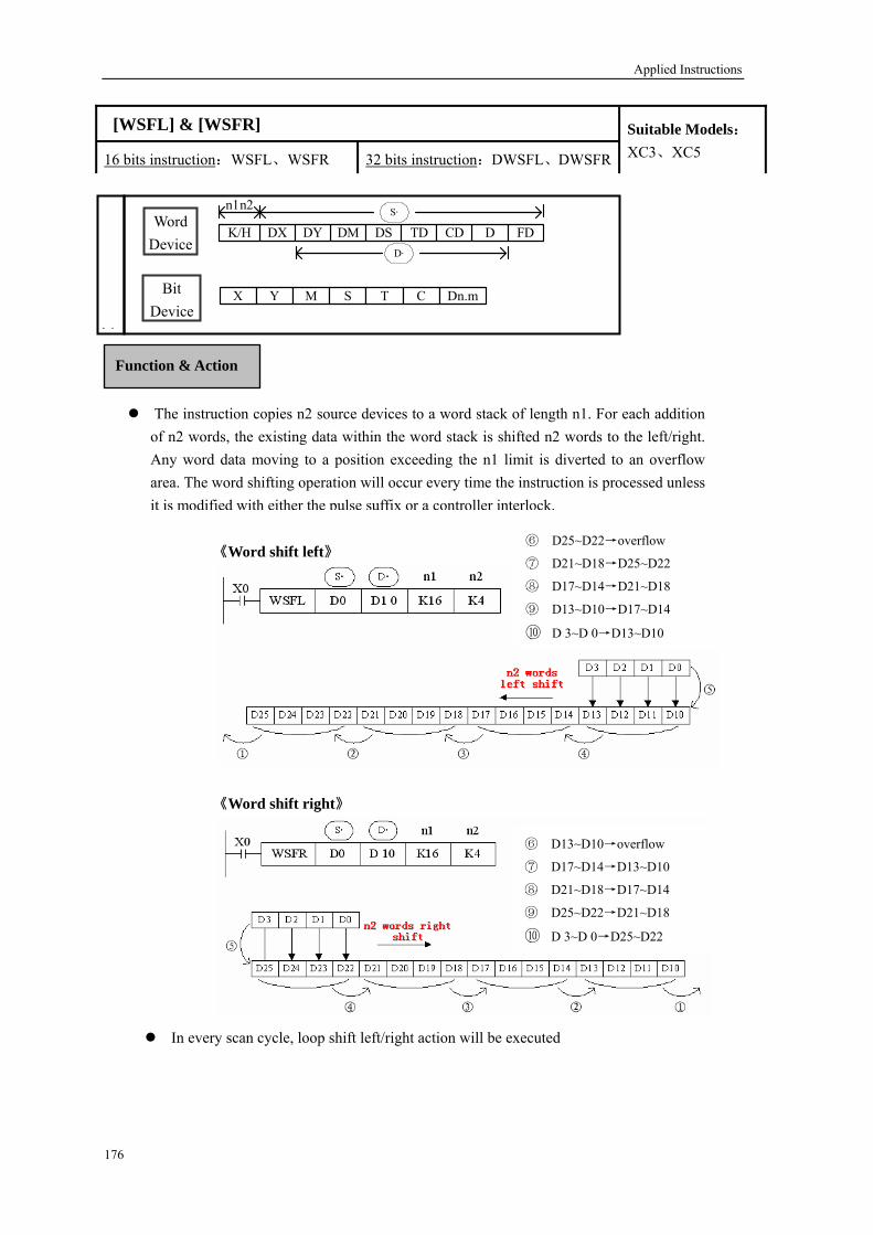
Applied Instructions
n2 字左移
n2 字右移
《Word shift left》
《Word shift right》
Function & Action
The instruction copies n2 source devices to a word stack of length n1. For each addition of n2 words, the existing data within the word stack is shifted n2 words to the left/right. Any word data moving to a position exceeding the n1 limit is diverted to an overflow area. The word shifting operation will occur every time the instruction is processed unless it is modified with either the pulse suffix or a controller interlock.
⑥ D13~D10→overflow
⑦ D17~D14→D13~D10
⑧ D21~D18→D17~D14
⑨ D25~D22→D21~D18
⑩ D 3~D 0→D25~D22
In every scan cycle, loop shift left/right action will be executed
[WSFL] & [WSFR]
16 bits instruction:WSFL、WSFR 32 bits instruction:DWSFL、DWSFR
Suitable Models: XC3、XC5
⑥ D25~D22→overflow
⑦ D21~D18→D25~D22
⑧ D17~D14→D21~D18
⑨ D13~D10→D17~D14
⑩ D 3~D 0→D13~D10
Word Device
Bit Device
X Y M S T C Dn.m
D FDDMDX DY DS TD CDK/H
n1n2
D·
S·
176

Applied Instructions
-8. Data Con5 vert
Mnemonic Function WTD Single word integer converts to double word integer FLT 32 bits integer converts to float point
FLTD 64 bits integer converts to float point INT Float point converts to integer BIN BCD convert to binary BCD Binary converts to BCD ASC Hex. converts to ASCII HEX ASCII converts to Hex.
DECO Coding ENCO High bit coding
ENCOL Low bit coding
177

Applied Instructions
WTD D0 D10X0
S· D·
High bits Low bits
D11 D10
0 or 1 D0
Function & Action
(D0) → (D11,D10) Single Word Double Word
When single word D0 is positive integer, after executing this instruction, the high bit of double word D10 is 0.
When single word D0 is negative integer, after executing this instruction, the high bit of double word D10 is 1.
[WTD]
16 bits instruction:WTD 32 bits instruction:-
Suitable Models: XC3、XC5
Word Device
Bit Device
X Y M S T C Dn.m
D FDDMDX DY DS TD CDK/HD·
S·
178

Applied Instructions
《16 Bits》
《
32 Bits》
DFLT D10 D12
S· D·
《
X0
64 Bits》
FLTD D10 D14
S· D·X0
Function & Action
(D11,D10)→ (D13,D12)
Binary float point BIN integer
(D10) → (D13,D12)
BIN integer Binary fl ooat p int
(D13,D12,D11,D10)→ (D17,D16,D15,D14)
BIN integer Binary float point
FLT D10 D12
S· D·X0
[FLT] & [FLTD]
16 bits instruction:FLT 32 bits instruction:DFLT
Suitable Models: XC3、XC5
Word Device
Bit Device
D FDDMDX DY DS TD CDK/HD·
S· S·
X Y M S T C Dn.m
Convert H will auto convert by the float op .
The instr
BIN integer to binary float point. As the constant K、
eration instruction, so this FLT instruction can’t be useduction is contrary to INT instruction.
179

Applied Instructions
《 位》
16
INT D10 D20
S· D·X0
《32 位》
DINT D10 D20
S· D·X0
Function & Action
(D11,D10) → (D20)
inary Floating BIN integer
Give up the data after the decimal dot B
(D11,D10) → (D20,D21)
Binary Floating BIN integer
Give up the data after the decimal dot
The binary source number is converted into an BIN integer and stored at the destination device. Abandon the value behind the decimal point.
This instruction is contrary to FLT instruction. When the result is 0, the flag bit is ON。
When converting, less than 1 and abandon it, zero flag is ON. 16 bits operation:-32,768~32,767 32 bits operation:-2,147,483,648~2,147,483,647
[INT]
16 bits instruction:- 32 bits instruction:INT
Suitable Models: XC3、XC5
Word Device
Bit Device
D FDDMDX DY DS TD CDK/HD·
S·
X Y M S T C Dn.m
180
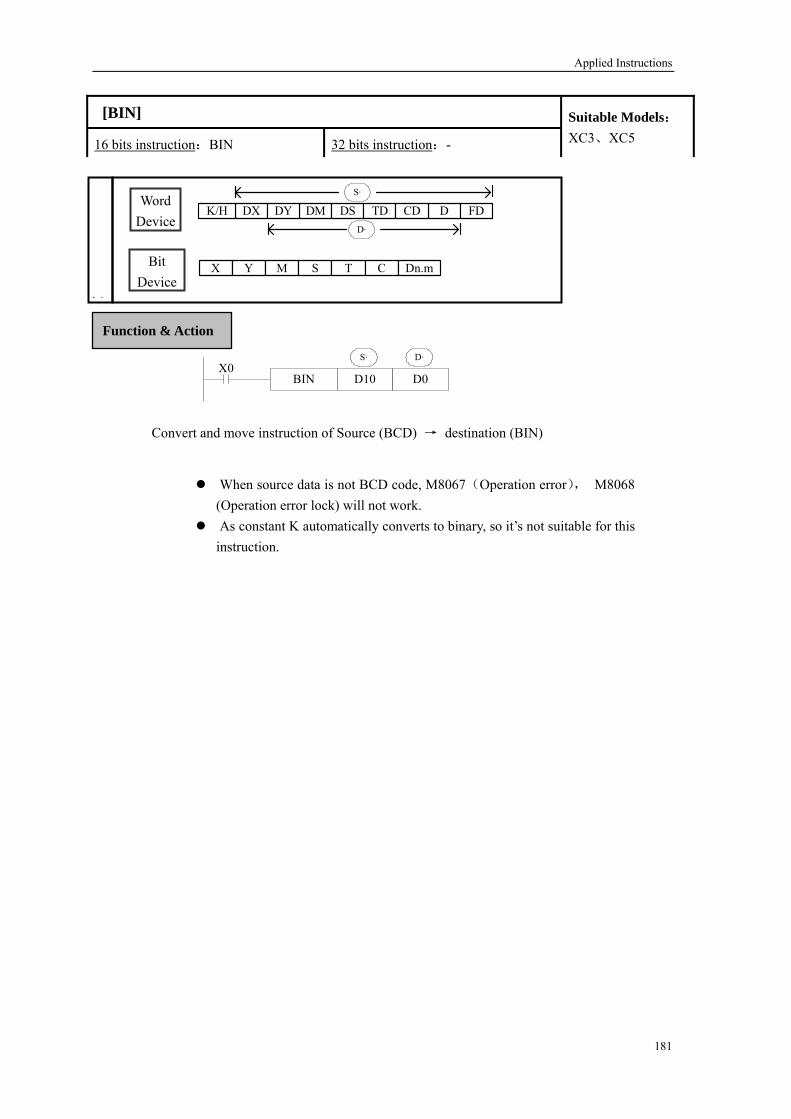
Applied Instructions
BIN D10 D0
S· D·X0
Function & Action
Convert and move instruction of Source (BCD) → destination (BIN)
When source data is not BCD code, M8067(Operation error), M8068 (Operation error lock) will not work.
As constant K automatically converts to binary, so it’s not suitable for this instruction.
[BIN]
16 bits instruction:BIN 32 bits instruction:-
Suitable Models: XC3、XC5
Word Device
Bit Device
D FDDMDX DY DS TD CDK/HD·
S·
X Y M S T C Dn.m
181

Applied Instructions
BCD D10 D0
S· D·X0
Function & Action
Convert and move instruction of source (BIN)→destination (BCD).
This instruction can be used to output data directly to a seven-segment display.
[BCD]
16 bits instruction:BCD 32 bits instruction:-
Suitable Models: XC3、XC5
Word Device
X Y M S T C Dn.m
D FDDMDX DY DS TD CDK/HD·
S·
Bit Device
182

Applied Instructions
《16 bits convert mode》
ASCI D100 D200 K4
S· D· nX0
Convert each bit of source’s (S) Hex. format data to be ASCII code, move separately to the high 8 bits and low 8 bits of destination (D). The convert alphanumeric number is assigned with n. (D) is low 8 bits, high 8 bits, store ASCII data.
The convert result is the following:
n
D K1 K2 K3 K4 K5 K6 K7 K8 K9
D200 down [C] [B] [A] [0] [4] [3] [2] [1] [8] D200 up [C] [B] [A] [0] [4] [3] [2] [1] D201 down [C] [B] [A] [0] [4] [3] [2] D201 up [C] [B] [A] [0] [4] [3] D202 down [C] [B] [A] [0] [4] D202 up [C] [B] [A] [0] D203 down [C] [B] [A] D203 up [C] [B] D204 down
[C]
Function & Action
Assign start device: (D 0(D101)=1234H (D102)=5678H
100)= ABCH [0]=30H [1]=31H [5]=35H
]=41H [2]=32H [6]=36H [B]=42H [3]=33H [7]=37H [C]=43H [4]=34H [8]=38H
[ASCI]
16 bits instruction:ASCI 32 bits instruction:-
Suitable Models: XC3、XC5
Word Device
Bit Device
X Y M S T C Dn.m
D FDDMDX DY DS TD CDK/HD·
S·
[A
183

Applied Instructions
《16 bits switch mode》
HEX D200 D100 K4K4
S· D·X0
The convert of the upward program is the following: 时
n=k4
nn
0 1 0 0 0 0 0
Applied Instructions
184
《16 bits switch mode》
HEX D200 D100
S· D·X0
The convert of the upward program is the following: 时
n=k4
0 1 0 0 0 0 0 1 0 0 1 1 0 0 0 0D200
41H→[A] 30H→[0]
0 1 0 0 0 0 1 1 0 1 0 1 0 0 1 0D201
43H→[C] 42H→[B]
0 0 0 0 1 0 1 0 1 0 1 1 1 1 0 0D202
0 A B C
[HEX]
16 bits instruction:HEX 32 bits instruction:-
Suitable Models: XC3、XC5
Word
Funct tion ion & Ac
(S·)
ASCII Code
HEX Convert
D200 down 30H 0 D200 up 41H A D201 down 42H B D201 up 43H C D202 down 31H 1 D202 up 32H 2 D203 down 33H 3 D203 up 34H 4 D204 down 35H 5
(D·)
nD102 D101 D100
1 ···0H 2 ··0AH 3 ·0ABH4
Not change to be 0
0ABCH 5 ···0H ABC1H 6 ··0AH BC12H 7 ·0ABH C123H 8
0ABCH 1234H 9 ···0H ABC1H 2345H
Convert the high and low 8 bits in source to HEX data. Move 4 bits every time to destination. The convert alphanumeric number is assigned by n.
Device
Bit Device
X Y M S T C Dn.m
D FDDMDX DY DS TD CDK/HD·
S·
184
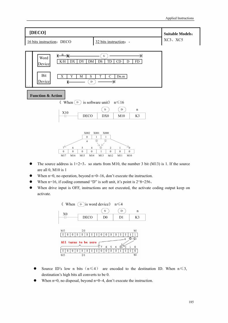
Applied Instructions
①②
③
《 When is software unit》 n≤16
DX0DECO M10 K3X10
nS· D·
0 1 1
0 0 0 1 0 0 0
X002 X001 X000
M17 M16 M15 M14 M13 M12 M11 M10
7 6 5 4 2 1 0
4
0
《 When is word device》 n≤4
D0DECO D1 K3X0
nS· D·
③
Function & Action D·
The source address is 1+2=3,so starts from M10, the number 3 bit (M13) is 1. If the source are all 0, M10 is 1
When n=0, no operation, beyond n=0~16, don’t execute the instruction. When n=16, if coding command “D” is soft unit, it’s point is 2^8=256。 When drive input is OFF, instructions are not executed, the activate coding output keep on
activate.
D·
Source ID’s low n bits(n≤4) are encoded to the destination ID. When n≤3, destination’s high bits all converts to be 0.
When n=0, no disposal, beyond n=0~4, don’t execute the instruction.
[DECO]
16 bits instruction:DECO 32 bits instruction:-
Suitable Models: XC3、XC5
Word Device
Bit Device
X Y M S T C Dn.mD·
S·
D FDDMDX DY DS TD CDK/H
n
185

Applied Instructions
③
③
①②
①②
All be 0
All be 0
Be ignored
《 When is bit device》 n≤16
M10ENCO D10 K3X0
nS· D·
0 0 0 1 0 1 0M17 M16 M15 M14 M13 M12 M11 M10
7 6 5 4 2 1 00
0 0 0 0 0 0 0 0 0 0 0 0 0 0 1 1D10b15
b0
4
《 When is word device》 n≤4
D0ENCO D1 K3X1
nS· D·
0 1 0 1 0 1 0 1 0 0 0 0 1 0 1 0
0 0 0 0 0 0 0 0 0 0 0 0 0 0 1 1
7 6 5 4 2 1 0
D0
D1b15
b15 b0
b0
4
Function & Action
S·
S·
If many bits in the source ID are 1, ignore the low bits. If source ID are all 0, don’t execute the instructions.
When drive input is OFF, the instruction is not executed, encode output don’t change. When n=8, if encode instruction’s “S” is bit unit, it’s point number is 2^8=256
[ENCO]
16 bits instruction:ENCO 32 bits instruction:-
Suitable Models: XC3、XC5
Word Device
Bit Device
X Y M S T C Dn.mS·
S·
D FDDMDX DY DS TD CDK/HD·n
186

Applied Instructions
187
③
③
①②
①②
All be 0
All be 0
Be ignored
《 If is bit device》 n≤16
Function & Action
[ENCOL]
16 bits instruction:ENCOL 32 bits instruction:-
Suitable Models: XC3、XC5
Word Device
Bit Device
S·
D FDDMDX DY DS TD CDK/HD·n
X Y M S T C Dn.mS·
M10ENCOL D10 K3X0
nS· D·
0 1 0 1 0 0 0M17 M16 M15 M14 M13 M12 M11 M10
7 6 5 4 2 1 00
0 0 0 0 0 0 0 0 0 0 0 0 0 0 1 1D10b15
b0
4
《 是字软元件时》 n≤16
D0ENCOL D1 K3X1
nS· D·
0 1 0 1 0 1 0 1 0 0 1 0 1 0 0 0
0 0 0 0 0 0 0 0 0 0 0 0 0 0 1 1
7 6 5 4 2 1 0
D0
D1b15
b15 b0
b0
4
S·
S·
If many bits in the source ID are 1, ignore the high bits. If source ID are all 0, don’t execute the instructions.
When drive input is OFF, the instruction is not executed, encode output don’t change. When n=8, if encode instruction’s “S” is bit unit, it’s point number is 2^8=256

Applied Instructions
5-9. Floating Operation
Mnemonic Function ECMP Float Compare EZCP Float Zone Compare EADD Floa Addt ESUB Float Subtract EMUL Float Multiplication EDIV Float Division ESQR Float Square Root SIN Sine COS Cosine TAN Tangent
188
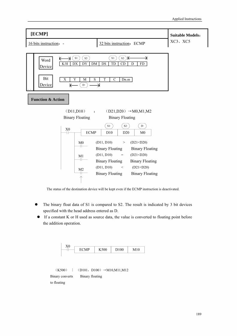
Applied Instructions
189
Function & Action
(D11,Binary
ECMP D10 D20 M0
M0
M1
M2
X0D·S1· S2·
D10) : (D21,D20)→M0,M1,M2 Floating Binary Floating
(D11, D10) > (D21<D20)
Binary Floating Binary Floating
(D11, D10) = (D21<D20)
Binary Floating Binary Floating
(D11, D10) < (D21<D20)
Binary Floating Binary Floating
The st ation device will be kept even if the ECMP instruction is deactivated. atus of the destin
ECMP K500 D100 M10X0
The binary float data of S1 is compared to S2. The result is indicated by 3 bit devices specified with the head address entered as D.
If a constant K or H used as source data, the value is converted to floating point before the addition operation.
(K500) ∶ (D101,D100)→M10,M11,M12 Binary converts Binary floating
to floating
[ECMP]
16 bits instruction:- 32 bits instruction:ECMP
Suitable Models: XC3、XC5
Word Device
Bit Device
D FDDMDX DY DS TD CDK/H
S1· S2· S1· S2·
X Y M S T C Dn.mD·

Applied Instructions
190
Compare a float range with a float value.
EZCP D10 D20 D0
M3
M4
M5
X0S1· S2·
M3
D1· D2·
The data of S1 is compared to the data of S2. The result is indicated by 3 bit devices specified with the head address entered as D.
If a constant K or H used as source data, the value is converted to floating point before the addition operation.
EZCP K10 K2800 D5 M0X0
Please set S1<S2, when S2>S1, see S2 as the same with S1 and compare them.
Function & Action
(D20, D21) > (D1, D0) ON
Binary Floating Binary Floating
(D21,D10) ≤ (D1,D0) ≤ (D31,D30) ON
Binary Floating Binary Floating Binary Floating
(D1, D0) > (D31, D30) ON
Binary Floating Binary Floating
The status of the destination device will be kept even if the EZCP instruction is deactivated.
(K10) ∶ [D6,D5] ∶ (K2800)→M0,M1,M2
Binary converts Binary Floating Binary converts
to Floating to Floating
[EZCP]
16 bits instruction:- 32 bits instruction:ECMP
Suitable Models: XC3、XC5
Word Device
Bit Device
X Y M S T C Dn.mD·
D FDDMDX DY DS TD CDK/HS1· S2· S3·
S1· S2· S3·
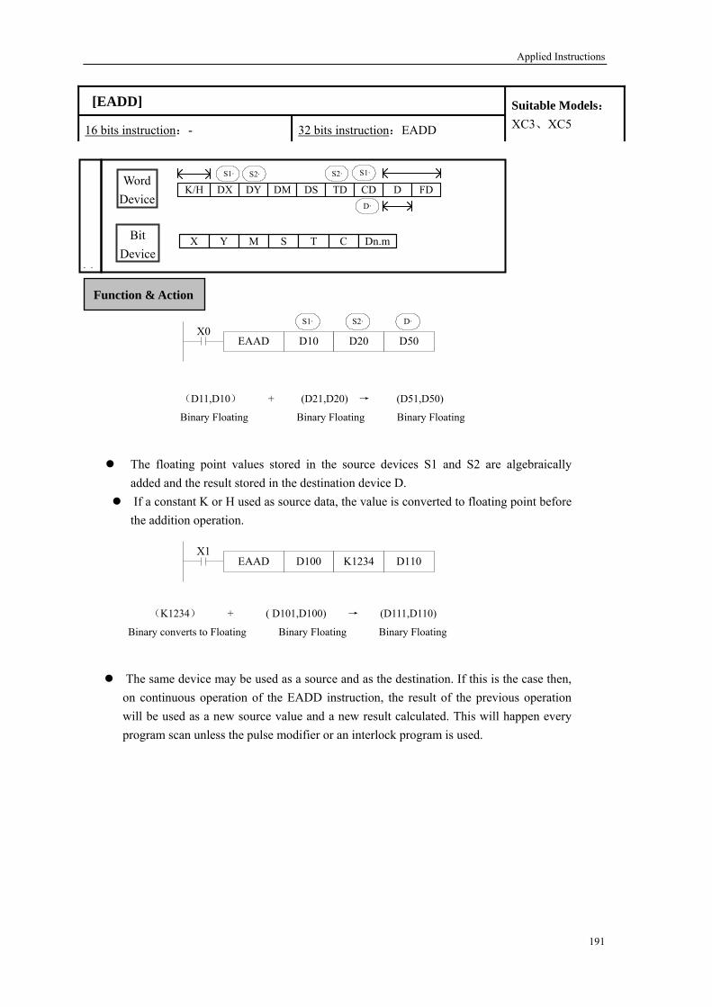
Applied Instructions
EAAD D10 D20 D50
S1· S2· D·X0
EAAD D100 K1234 D110X1
Function & Action
(D11,D10) + (D21,D20) → (D51,D50)
Binary Floating Binary Floating Binary Floating
The floating point values stored in the source devices S1 and S2 are algebraically added and the result stored in the destination device D.
If a constant K or H used as source data, the value is converted to floating point before the addition operation.
(K1234) + ( D101,D100) → (D111,D110)
Binary converts to Floating Binary Floating Binary Floating
The same device may be used as a source and as the destination. If this is the case then, on continuous operation of the EADD instruction, the result of the previous operation will be used as a new source value and a new result calculated. This will happen every program scan unless the pulse modifier or an interlock program is used.
[EADD]
16 bits instruction:- 32 bits instruction:EADD
Suitable Models: XC3、XC5
Word Device
Bit Device
D FDDMDX DY DS TD CDK/HS1· S2· S2·
D·
S1·
X Y M S T C Dn.m
191

Applied Instructions
ESUB D10 D20 D50
S1· S2· D·X0
The floating point value of S2 is subtracted from the floating point value of S1 and the result stored in destination device D.
If a constant K or H used as source data, the value is converted to floating point before the addition operation.
ESUB D100K1234 D110X1
Function & Action
(D11,D10) - (D21,D20) → (D51,D50)
Binary Floating Binary Floating Binary Floating
(K1234) - (D101,D100) → (D111,D110)
Binary converts to Floating Binary Floating Binary Floating
The same device may be used as a source and as the destination. If this is the case then, on continuous operation of the EADD instruction, the result of the previous operation will be used as a new source value and a new result calculated. This will happen every program scan unless the pulse modifier or an interlock program is used.
[ESUB]
16 bits instruction:- 32 bits instruction:ESUB
Suitable Models: XC3、XC5
Word Device
Bit Device
X Y M S T C Dn.m
D FDDMDX DY DS TD CDK/HS1· S2· S2·
D·
S1·
192

Applied Instructions
EMUL D10 D20 D50
S1· S2· D·X0
EMUL D100K100 D110X1
Function & Action
(D11,D10) × (D21,D20) → (D51,D50)
Binary Floating Binary Floating Binary Floating
The floating value of S1 is multiplied with the floating value point value of S2. The result of the multiplication is stored at D as a floating value.
If a constant K or H used as source data, the value is converted to floating point before the addition operation.
(K100) × (D101,D100) → (D111,D110)
Binary converts to Floating Binary Floating Binary Floating
[EMUL]
16 bits instruction:- 32 bits instruction:EMUL
Suitable Models: XC3、XC5
Word Device
Bit Device
D FDDMDX DY DS TD CDK/HS1· S2· S2·
D·
S1·
X Y M S T C Dn.m
193

Applied Instructions
EDIV D10 D20 D50
S1· S2· D·X0
The floating point value of S1 is divided by the floating point value of S2. The result of the division is stored in D as a floating point value. No remainder is calculated.
If a constant K or H used as source data, the value is converted to floating point before the addition operation.
EDIV D100 K100 D110X1
Function & Action
(D11,D10)÷(D21,D20)→(D51,D50)
Binary Floating Binary Floating Binary Floating
(D101,D100) ÷ (K100) → (D111,D110)
Binary Floating Binary converts to Floating Binary Floating
If S2 is zero then a divide by zero error occurs and the operation fails.
[EDIV]
16 bits instruction:- 32 bits instruction:EDDIV
Suitable Models: XC3、XC5
D FDDMDX DY DS TD CDK/HS1· S2· S2·
D·
S1·
X Y M S T C Dn.m
Word Device
Bit Device
194

Applied Instructions
195
ESQR D10 D20X0
S· D·
ESQR K1024 D110X1
Function & Action
(D11,D10) →(D21,D20)
Binary Floating Binary Floating
A square root is performed on the floating point value in S the result is stored in D. If a constant K or H used as source data, the value is converted to floating point before
the addition operation.
(K1024) → (D111,D110)
Binary converts to Floating Binary Floating
When the result is zero, zero flag activates Only when the source data is positive will the operation be effective. If S is negative then
an error occurs and error flag M8067 is set ON, the instruction can’t be executed.
[ESQR]
16 bits instruction:- 32 bits instruction:ESQR
Suitable Models: XC3、XC5
[SIN]
16 bits instruction:- 32 bits instruction:SIN
Suitable Models: XC3、XC5
Word D FDDMDX DY DS TD CDK/H
D·
S· S·
Device
Bit D
X Y M S T C Dn.mevice
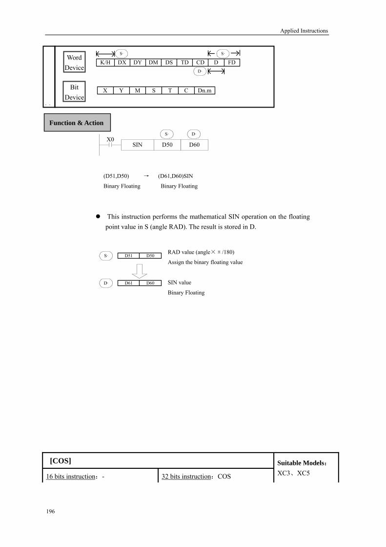
Applied Instructions
SIN D50 D60X0
S· D·
D51 D50
D61 D60
S·
D·
Function & Action
(D51,D50) → (D61,D60)SIN
Binary Floating Binary Floating
This instruction performs the mathematical SIN operation on the floating point value in S (angle RAD). The result is stored in D.
RAD value (angle×π/180)
Assign the binary floating value
SIN value
Binary Floating
[COS]
16 bits instruction:- 32 bits instruction:COS
Suitable Models: XC3、XC5
Word Device
Bit Device
X Y M S T C Dn.m
D FDDMDX DY DS TD CDK/HD·
S· S·
196

Applied Instructions
COS D50 D60X0
S· D·
D51 D50
D61 D60
S·
D·
Function & Action
(D51,D50)RAD → (D61,D60)COS
Binary Floating Binary Floating
This instruction performs the mathematical COS operation on the floating point value in S (angle RAD). The result is stored in D.
RAD value (angle×π/180)
Assign the binary floating value
COS value
Binary Floating
[TAN]
16 bits instruction:- 32 bits instruction:TAN
Suitable Models: XC3、XC5
Word Device
Bit Device
X Y M S T C Dn.m
D FDDMDX DY DS TD CDK/HD·
S· S·
197

Applied Instructions
TAN D50 D60X0
S· D·
D51 D50
D61 D60
S·
D·
Function & Action
(D51,D50)RAD → (D61,D60)TAN
Binary Floating Binary Floating
This instruction performs the mathematical TAN operation on the floating point value in S. The result is stored in D.
RAD value (angle×π/180)
Assign the binary floating value
TAN value
Binary Floating
Word Device
Bit Device
D FDDMDX DY DS TD CDK/HD·
S· S·
X Y M S T C Dn.m
198

Applied Instructions
5-10. Clock O
peration
Mnemonic Function TCMP Time Compare TZCP Time Zone Compare TADD Time Add TSUB Time Subtract TRD Read RTC data TWR Set RTC data
Note:The models without clock can not use these instructions.
199

Applied Instructions
Function & Action
Compare the assigned time with time data.
The status of the destination devices is kept, even if the TCMP instruction is deactivated.
:Assign the compare standard “Hour” :Assign the compare standard “Minute” :Assign the compare standard “Second”
S1·
S2·
S3·
「 , , 」represent hours, minutes and seconds respectively. This time is compared to the time value in the 3 data devices specified by the head address , The result is indicated in the 3 bit devices specified by the head address
S1· S2· S3·
S·
D·
:Assign the “Hour” of clock data +1 :Assign the “Minute” of clock data +2 :Assign the “Second” of clock data
S ·
S ·
S ·
, +1, +2 :According to the compare result, the 3 devices output ON/OFF.
The valid range of “Hour” is「0~23」. The valid range of “Minute” is「0~59」. The valid range of “Second” is「0~59」.
D· D· D·
Time Compare [TCMP]
16 bits instruction:DIV 32 bits instruction:DDIV
Suitable Models: XC3、XC5
Word Device
Bit Device
X Y M S T C Dn.mD·
S·
D FDS1· S2· S3·
DMDX DY DS TD CDK/H
200
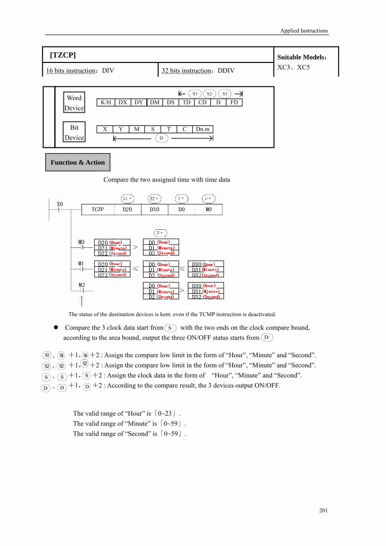
Applied Instructions
Function & Action
即使使用 X000=OFF 停止执行 TZCP 指令时,
仍然保持 X000 变为 OFF 以前的状态。
M0~M2
Compare the two assigned time with time data
Comp 3 clock data start from with the two ends on the clock compare bound, accord e area bound, output the three ON/OFF status starts from
are the ing to th
S·
D·
, +1, +2 : Assign the compare low limit in the form of “Hour”, “Minute” and “Second”. , +1, +2 : Assign the compare low limit in the form of “Hour”, “Minute” and “Second”.
, +1, +2 : Assign the clock data in the form of “Hour”, “Minute” and “Second”. ices output ON/OFF.
, +1, +2 : According to the compare result, the 3 dev
S1· S1· S1·
S2· S2·S2·
S· S· S·
D·D·
The valid range of “Hour” is「0~23」. lid range of “Minute” is「0~59」. id range of “Second” is「0~59」.
[TZCP]
16 bits instruction:DIV 32 bits instruction:DDIV
Suitable Models: XC3、XC5
Word Device
Bit Device
D FDDMDX DY DS TD CDK/HS1· S2· S3·
X Y M S T C Dn.mD·
The status of the destin devices is kept, even if the TCMP instruction is deactivated. ation
D·
The vaThe val
201

Applied Instructions
D10 (Hour)D11 (Minute)
D12 (Second)
D20 (Hour)D21 (Minute)
D22 (Second)
D30 (Hour)D31 (Minute)
D32 (Second)+
S1 S2 D
10 hour 20 min. 30 sec. 3 hour 20 min. 10 sec. 13 hour 40 min. 40 sec.
18 (Hour)10 (Minute)
30 (Second)
10 (Hour)20 (Minute)
5 (Second)
4 (Hour)30 (Minute)
35 (Second)+
S1 S2 D
18 hour 10 min. 30 sec. 3 hour 20 min. 10 sec. 4 hour 30 min. 35 sec.
Function & Action
Each of S1, S2 and D specify the head address of 3 data devices to be used a time value. The time value in S1 is added to the value in S2, the result is stored to D as a new time value.
If the addition of the two times re a value greater than 24 hours, the value of the result is the time remaining abov urs. When this happens the M8022 is
sults ine 24 ho carry flag
When the result is 0(0 Hour 0 Minute 0 Second),Set zero flag ON.
The valid range of “Hour” is「0~23」. The valid range of “Minute” is「0~59」. The valid range of “Second” is「0~59」.
(D10, D11, D12)+(D20, D21, D22)→(D30, D31, D32)
TADD D10 D20 D30X0
S1· S2· D·
[TADD]
16 bits instruction:DIV 32 bits instruction:DDIV
Suitable Models: XC3、XC5
Word Device
Bit Device
D FDDMDX DY DS TD CDK/HS1· S2·
D·
X Y M S T C Dn.m
202
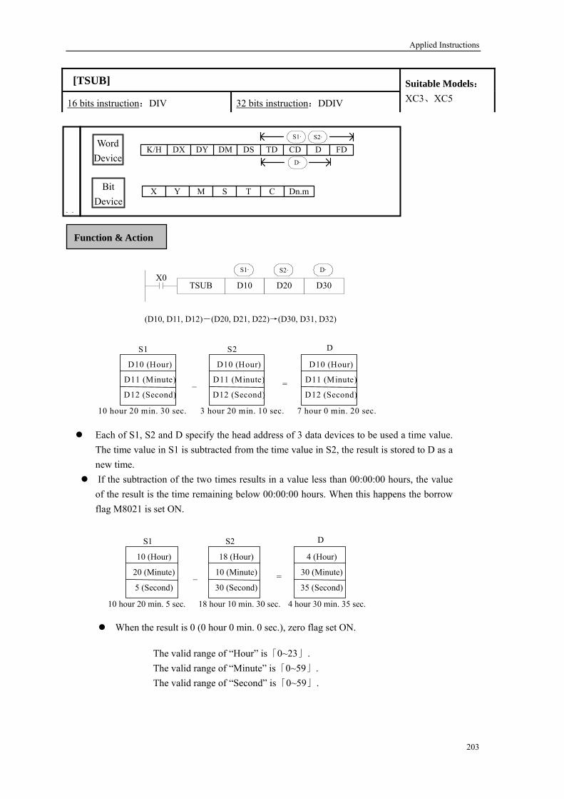
Applied Instructions
203
TSUB D10 D20 D30X0
S1· S2· D·
D10 (Hour)
D11 (Minute)
D12 (Second)
D10 (Hour)
D12 (Second)
D11 (Minute)
D10 (Hour)
D11 (Minute)
D12 (Second)_ =
S1 S2 D
10 hour 20 min. 30 sec. 3 hour 20 min. 10 sec. 7 hour 0 min. 20 sec.
10 (Hour)
20 (Minute)
5 (Second)
18 (Hour)
10 (Minute)
30 (Second)
4 (Hour)
30 (Minute)
35 (Second)_ =
S1 S2 D
10 hour 20 min. 5 sec. 18 hour 10 min. 30 sec. 4 hour 30 min. 35 sec.
Function & Action
Each of S1, S2 and D specify the head address of 3 data devices to be used a time value. The time value in S1 is subtracted from the time value in S2, the result is stored to D as a new time.
If the subtraction of the two times results in a value less than 00:00:00 hours, the value of the result is the time remaining below 00:00:00 hours. When this happens the borrow flag M8021 is set ON.
When the result is 0 (0 hour 0 min. 0 sec.), zero flag set ON.
The valid range of “Hour” is「0~23」. The valid range of “Minute” is「0~59」. The valid range of “Second” is「0~59」.
(D10, D11, D12)-(D20, D21, D22)→(D30, D31, D32)
[TSUB]
16 bi ts instruction:DIV 32 bits instruction:DDIV
Suitable Models: XC3、XC5
Word Device
D FDDMDX DY DS TD CDK/HS1· S2·
D·
Bit Device
X Y M S T C Dn.m
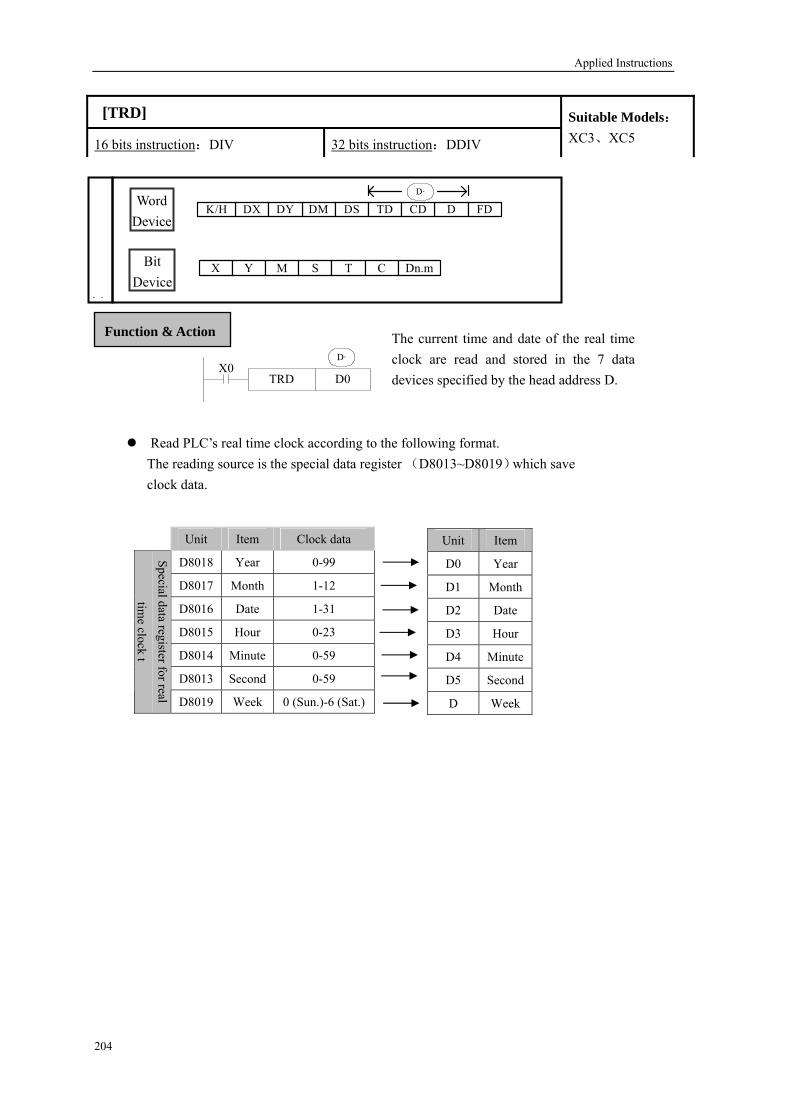
Applied Instructions
[TRD]
204
16 bits
Suitable Models:
instruction:DIV 32 bits instruction:DDIV XC3、XC5
Word ice
TRD D0X0
D·
Function & Action The current time and date of the real time clock are read and stored in the 7 data devices specified by the head address D.
Read PLC’s real time clock according to the following format. The reading source is the special data register (D8013~D8019)which save clock data.
Dev
Bit Device
X Y M S T C Dn.m
D FDDMDX DY DS TD CDK/HD·
Unit Item Clock data
D8018 Year 0-99
D8017 Month 1-12
D8016 Date 1-31
D8015 Hour 0-23
D8014 Minute 0-59
D8013 Second 0-59
Special data register for real
time clock t
D8019 Week 0 (Sun.)-6 (Sat.)
Unit Item
D0 Year
D1 Month
D2 Date
D3 Hour
D4 Minute
D5 Second
D Week

Applied Instructions
TWR D10X0
S·
Function & Action
The 7 data devices specified with the
head address S are sed to set a ne
Write the set clock data into PLC’s real time clock. In order to write real time clock, the 7 data devices specified with the head address should be pre-set. S·
After executing TWR instruction, the time in real time clock will ly change to be the new set time. So, when setting the time it is a
then drive the instruction when the real time reaches this value.
[TWR]
16 bits instruction:DIV 32 bits instruction:DDIV
Suitable Models: XC3、XC5
Word Device
Bit Device
X Y M S T C Dn.m
D FDDMDX DY DS TD CDK/HS·
Unit Item Clock data
D0 Year 0-99
D1 Month 1-12
D2 Date 1-31
D3 Hour 0-23
D4 Minute 0-59
D5 Second 0-59
Data for clock setting
D6 Week 0 (Sun.)-6 (Sat.)
Unit Item
D8018 Year
D8017 Month
D8016 Date
D8015 Hour
D8014 Minute
D8013 Second
D8019 Week
Special data register for real
time clock t
immediategood idea to set the source data to a time a number of minutes ahead and
205
Applied Instructions
In this chapter, we introduce the functions of high-speed count input, high-speed pulse output and MODBUS communication instructions of XC series PLC.
6. Special Function Instructions(XC3/XC5)
6-1.High-speed Count
6-2.Pulse Uutput
6-3.Modbus Instructions
6-4.Free Format Communication
6-5.PWM Pulse Modulate
6-6.Frequency Testing
6-7.Precise Time
6-8.Interrupt Function
6-9.CANBUS Communication(XC5 Series)
206

Applied Instructions
6-1. High-speed Count
High-speed Count Function
counter, you can e mode count, the
ncy ca
XC series PLC all have high speed count function. By choosing different realize count function of increment mode, pulse + direction input mode, AB phasfreque n reach 200KHz.
The Assignment of Count Input Ports 1, In the following table, we list how many high speed counters are there in XC series PLC:
High-speed counters
PLC Model Increment Mode Pulse+ Direction Mode AB Phase Mode
XC3-14 4 2 2 XC3-24/XC3-32 5 3 3
XC3 Series
XC3-48/XC3-60 4 2 2 XC5-32 2 1 1 XC5
Series XC5-48/XC5-60 5 3 3
207

Applied Instructions
2, About the definition of high speed counter’s input terminals, please refer to the following table:
When X input terminals are not used as high speed input port, they could be used as common input terminals.
[U]---count pulse input [Dir]---count direction judgment (OFF means +, ON means -) [A]---A phase input [B]---B phase input
Increment Mode Pulse+ Direction Input
Mode AB Phase Mode
C600 C602 C604 C606 C608 C610 C612 C614 C616C618 C620C622 C624 C626 C628 C630 C632 C634
X000 U U B
X001 Dir A
X002
X003 U U B
X004 Dir A
X005
X006 U U B
X007 Dir A
X010
X011 U
X012
U
Increment Mode Pulse+ Direction Input
Mode AB Phase Mode
C600 C602 C604 C606 C608 C610 C612 C614 C616 C618 C620C622 C624 C626 C628 C630 C632 C634
X000 U U B
X001 Dir A
X002 U U B
X003 Dir A
X004 U
X005 U
XC3-48、XC3-60 PLC models
XC3-24、XC3-32 AND XC5-48、XC5-60 PLC MODELS
208

Applied Instructions
209
3, About the high speed counters which don’t support four times frequency in AB phase high speed counters, please refer to the following table:
Input Mode of High Speed Counter’s Signal 1, Input Mode
Increment Mode: Under increment mode, input pulse signal, the count value increases with each pulse signal.
+1 +1 +1 +1 +1 +1 +1 +1
Pulse Input ON
OFF
Increment Mode Pulse+ Direction Input
Mode AB Phase Mode
C600 C602 C604 C606 C608 C610 C612 C614 C616 C618 C620C622 C624 C626 C628 C630 C632 C634
X000 U U B
X001 Dir A
X002 U
X003 U
X004 U B
X005 U Dir A
XC3-14 PLC MODELS
Increment Mode Pulse+ Direction Input
Mode AB Phase Mode
C600 C602 C604 C606 C608 C610 C612 C614 C616 C618 C620C622 C624 C626 C628 C630 C632 C634
X000 U U B
X001 Dir A
X002
X003 U
XC5-32 PLC MODELS
PLC MODELS High speed counters without four times counter
XC3-14 C630 XC3-24/ XC3-32 C632 XC3 Series XC3-48/ XC3-60 C630 XC5-32 -
XC5 Series XC5-48/ XC5-60 C632

Applied Instructions
Pulse + Direction input mode: Under pulse + direction input mode, both the pulse signal and direction signal are input, the count value increase/decrease according to the direction signal’s status.
+1 +1 +1 +1 -1 -1-1 -1
AB phase mode: U
nder AB phase mode, the count value increase/decrease according to the signal difference (A phase
and B phase)
+1 -1
2, Count Value High speed counter’s count bound: K-2,147,483,648 ~ K+2,147,483,647. If the count value
exceeds the bound, overflow or underflow will occur; if occur overflow, K+2,147,483,647 will change to be K-2,147,483,648, then go on counting; if occur underflow, K-2,147,483,648 will change to be K+2,147,483,647, then go on counting
3, Reset
High speed counter’s count format is software reset format
RST C600
C600M0
M1
K2000
Pulse input
Direction Dir
A phase input
B phase input
ON
OFF ON
OFF
ON
OFF
ON
OFF
See the right graph, when M0 is ON, C600 starts to count with the pulse input from X0 port; when M1 turns from OFF to ON, the status value and count value of C600 reset.
210

Applied Instructions
Connection of input terminal The following, we take C600 as the example to introduce the connection format. AB phase mode Pulse + Direction mode
COMCOM
X1X0
X3X2 X4
X5X6
COMCOM
X1X0
X3X2 X4
X5X6
Increment Mode
COMCOM
X1X0
X3X2 X4
X5X6
Program Example
The following, we take XC3-60 PLC model as the example to tell how to program with the high speed count:
RST C600
C600
RST C604
C604
M0
M1
M2
M3
K2000
D0(D1)
A phase input B phase input Pulse input
Direction input
Pulse input
When M0 is ON, C600counts with the OFF→ON from X000.
When M1 activates, reset when execute RST instruction.
When M2 is ON, C604 starts to count. The count input is X004, In this example, the set value is the content indirectly assigned in the data register.
See the graph, reset via M3 in the sequential control program.
Increment M
ode
211

Applied Instructions
212
RST C620
C620M4
M5
D0(D1)
RST C622
C622M6
M7
K100
RST C630
C630
Y002
K1000
RST C632
C632
Y004
D0(D1)
M8
M9
C630
M10
M11
C632
When M4 is ON, C620 counts with OFF→ON from X000, via OFF or ON status from X001, decide the count direction. If X001 is OFF, execute increase count; if X001 is ON, execute decrease count”.
When M6 is ON, C622 counts with OFF→ON from X000, via OFF or ON status from X002, decide the count direction. If X003 is OFF, execute increase count; if X003 is ON, execute decrease count”.
Pulse + Direction input m
ode
AB phase
mode
AB phase counter realize increase/decrease count by the judgment of A、B phase. The output contactor’s (correspond with the current value) action is the same with the preceding single phase counter.
When M8 is ON, C630 counts with the input X000 (B phase), X001(A phase) via interruption.
If M9 is ON, execute RST instruction to reset.
If the current value exceeds the set value, then Y002 is ON; If the current value is smaller than the set value, then Y002 is OFF
When M10 is ON, C632 starts to count. The count input is X002 (B phase)、X003(A phase).
Reset via M11. If the current value exceeds the set
value, then Y004 activates; If the current value is smaller than the set value, then Y004 is OFF
In the condition of A phase input is OFF→ON, if B phase input is OFF, the counter is increase count; if B phase input is ON, the counter is decrease count.
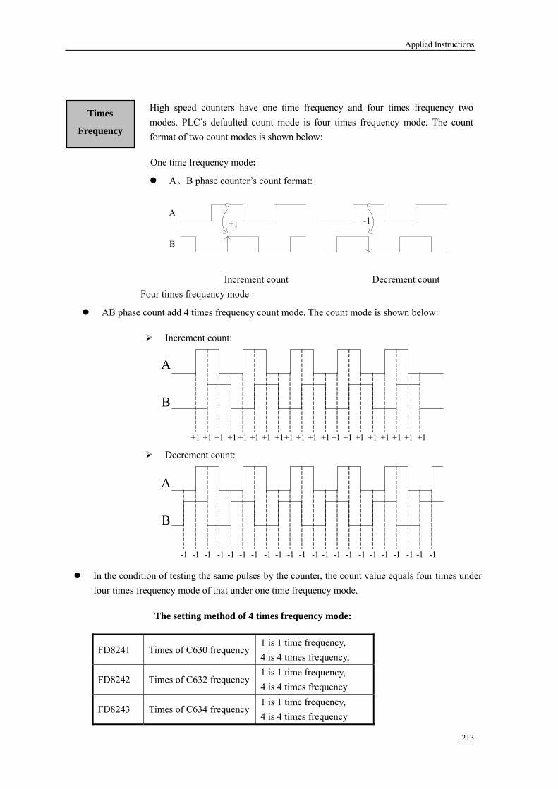
Applied Instructions
213
One time frequency mode:
+1 -1A
B
Increment count Decrement count Four times frequency mode
Increment count:
+1 +1 +1 +1
+1 +1 +1 +1+1 +1 +1 +1 +1 +1 +1 +1 +1 +1 +1 +1
A
B
Decrement count:
-1 -1 -1 -1 -1 -1 -1 -1 -1 -1 -1 -1 -1 -1 -1 -1 -1 -1 -1 -1 -1 -1
A
B
The setting method of 4 times frequency mode:
Times
Frequency
A、B phase counter’s count format:
AB phase count add 4 times frequency count mode. The count mode is shown below:
In c by the counter, the count value equals four times under four tim frequency mode.
the ondition of testing the same pulses es frequency mode of that under one time
High speed counters have one time frequency and four times frequency two modes. PLC’s defaulted count mode is four times frequency mode. The count format of two count modes is shown below:
4 is 4 times frequency,
FD8241 Times of C630 frequency 1 is 1 time frequency,
FD8242 Times of C632 frequency 1 is 1 time frequency, 4 is 4 times frequency
FD8243 Times of C634 frequency 1 is 1 time frequency, 4 is 4 times frequency

Applied Instructions
6-2. Pulse Output
Pulse Output Function
ormally XC3 series and XC5 series PLC have 2 channels pulse output. Via different instruction to rogram, you can realize single direction pulse output without speedup/speed-down; or you can realize ingle direction pulse output with speedup/speed-down; or you can realize multiply-segment, ositive/negative output and so on. The output frequency can reach 400K Hz.
Npsp
Y0COM0
Y1COM1
Y2COM2
Step Motor
Driver
ote: 1) To use pulse output, you should use PLC with transistor output. Such as XC3-14T-E or XC3-60RT-E etc.
2) XC5-32 PLC models have 4 channels (Y0, Y1, Y2, Y3) pulse output function.
Type and application of pulse output
1、 Single direction pulse output without speedup/speed-down • Frequency: 0~400KHz • Output terminals: Y0 or Y1 • Output mode: sequential or limited pulse output • Pulse number: 16 bits instructions 0~K32767
32 bits instructions 0~K2147483647 • Instructions: PLSY, PLSF PLSY: generate certain quantity pulse with the assigned frequency
PLSF: generate sequential pulse with changeable frequency form
N
214

Applied Instructions
PLSY Instruction:
PLSY K30 D1 Y0M0
S1· S2· D·
M8170RST M0
After finish outputting the set pulse number, output will auto stop.
PLSF Instruction:
PLSF D0 Y0M0
S· D·
Limited pulse output
Set pulse number
Sequential pulse output
Generate certain quantity pulse with the assigned frequency; support 32 bits instruction [DPLSY]. Assign the Frequency. Operands: K、TD、CD、D、FD Assign the generated pulse volume. Operands: K、TD、CD、D、FD
Assign Y port which generates pulse, can only output at Y000 or Y001
S1·
S2·
D·
When M0 is ON, PLSY instruction output pulse of 30Hz at Y0, the pulse number is assigned by D1, when sending pulse, coil M8170 sets ON. When the output pulse reach the set value, stop pulse output, coil M8170 sets OFF, reset M0.
Generate sequential pulse with changeable frequency form Support 32 bits instruction [DPLSF]. Assign the frequency. Operands: K、TD、CD、D、FD
Bound: 200~400KHz (If the set frequency is lower than 200Hz, output 200Hz) Assign Y port which generates pulse, can only output at Y000 or Y001 With the changing of the set frequency in D0, the output pulse frequency from Y0 changes.
D·
S·
Accumulate pulse number in register D8170
Continuously output pulse with the set frequency till pass the statement, then stop outputting.
215

Applied Instructions
Pulse output of single segment and single direction
2, One-direction pulse output with speedup/speed-down • Frequency: 0~400KHz • Speedup/speed-down time: Below 5000ms • Output terminals: Y0 or Y1 • Output Mode: Limited pulse • Pulse number: 16 bits instruction 0~K32767
32 bits instruction 0~K2147483647 • Instruction: PLSR PLSR: generate certain pulse with the assigned frequency and speedup/speed-down time.
PLSR K3000 D300 Y0M0
K300
S1· S2· S3· D·
M8170RST M0
When M0 is ON, PLSR starts pulse output, send assigned pulse number according to the assigned speedup/speed-down slope、highest frequency. To output with the constant speed, set the speedup/speed-down time as 0. If set the pulse number as H 7FFFFFFF, infinity pulse number will be sold out, at this time coil M8170 set ON.
When the output pulse number reaches the set value, stop pulse outputting, at this time coil M8170 set OFF, reset M000. See the following chart
Generate a certain quantity pulse with the assigned frequency; support 32 bits instruction [DPLSR]。 Highest frequency. Operands: K、TD、CD、D、FD Total output pulse number. Operands: K、TD、CD、D、FD
Speedup/speed-down time. Operands: K、TD、CD D、FD Assign Y number of output pulse, could only be output at Y000 or Y001
S1·
S2·
D ·
S3· 、
216

Applied Instructions
Pulse output of segments and single phase
PLSR D0 D100 Y3
RST M0
M0
M8170
S1· S2· D·
The instruction which generates a certain quantity pulse with the assigned frequency. An area with Dn or FDn as the start address. In the above example, D0 set the highest
frequency of segment 1 pulse, D1 set the highest frequency of segment 1 pulse, D2 set the highest frequency of segment 2 pulse, D3 set the highest frequency of segment 2 pulse, ……
if the set value of Dn, Dn+1 are both 0, it means segment finish. You can set at most 24 segments. Operands: D, FD
Speedup/speed-down time. Here the time means the speed time from start to the first segment’s speedup time, meantime, all segments’ frequency and time slope are defined. So the following speedup/speed-down speed follows them. Operands: K, TD, CD, D, FD
Assign the Y number of output pulse, can only output at Y000 or Y001 Support double words output DPLSR, here D0、D1 set the highest frequency of segment
1、D2、D3 set the pulse number of segment 1, D4、D5 set the highest frequency of segment 2、D6、D7 set the pulse number of segment 2……
S1·
S2·
D ·
217

Applied Instructions
3, Dual Pulse Output with speedup/speed-down
• y: 0~400KHz • Speedup/spe• Output Term• Direction ou ny Y • Output Mode: Limited number of pulse • Pulse Number: 16 bits instruction: 0~K32767
32 bits instruction: 0~K2147483647 Instruction: PLSR
PLSR: Generate certain pu gned frequency and speedup/speed-down time.
Dual Pulse Output with Speedup/Speed-down
Frequenced-down time: Below 5000ms inals: Y0 or Y1 tput terminal: A
lse with the assi
PLSR D0 D100 Y0
RST M0
M0
M8170
S1· S2·
Y3
D1· D2·
Generat tain pulse with the assigned frequency, speedup/speed-down time, pulse direction. which takes Dn or FDn with the start addr example, D0 set the max
of segment 1, D1 set pulse number of segment , D3 umber of segment 2, …… if Dn、Dn+1 are n set 24
segments at most. Operands: D, FD. Speedup/speed-down time, here the time means the speedup time from the start to the highest frequency. At the same time all segments’ frequency and time slope is defined, so the following speedup/speed-down format all do according to them. Operands: K、TD、CD、D、FD
Assign Y number of output pulse, can only output at Y000 or Y001 Assign Y number of output pulse direction, can be assigned at your will. E.g. In , if the pulse number is a positive value in segment 1, Y output ON; if be negative, Y is OFF. Please note: in once segment pulse output, pulse’s direction is only determined by the pulse number set value (positive or negative) of the first segment.
e ceress. In the precedingAn areaS1·
S2
1. D2 set the max frequency of segment 2 both 0, it means segment finish. You ca
frequencyset pulse n
·
D 1 ·
S1·D 2 ·
218

Applied Instructions
T]
4, Pulse Segment Switch [PLSNEX
Y0PLSNEXTM1
PLSY D0 D100 Y0M0
In the condition of pulse output reaches the highest frequency of current segment, and stably output, 1 turns from OFF to ON, then enter next pulse output with the speedup/speed-down time. lse output speedu is invalid.
if M In pu p/speed-down process, execute this instruction
lse Stop [STOP]
5, Pu
D0PLSRM0
M
D100 Y0
1
M8170
STOP Y0
RST M0
--------(the broken line)means the original pulse output curve
If M000 turns from OFF to ON, PLSY activates and Y000 output pulse, D0 assign the frequency, D001 assign the pulse number, D100 assign the speedup/speed-down time, when the output pulse number reaches the set value, stop pulse outputting. At the rising edge of M001, STOP instruction stop pulse outputting at Y000 immediately.
219

Applied Instructions
220
Connection of output terminals
Y0COM0
Y1COM1
Y2COM2
The following graph is connection of output terminals and step motor driver:
Y0PU
PUY1
PLC Side Step Motor Driver Side
Output port Y0: pulse output port 0 (Single Phase) Output port Y1: pulse output port 1 (Single Phase)

Applied Instructions
1, Concep
Note Items t of Step Frequency
, Frequency jump in segment pulse output
2
3, Pulse Output can’t realize dual output
D0PLSR D100 Y0M0
D200PLSR D1000 Y0M1
In one main program, you can’t write two or up to two pulse output instruction with the same output port Y.
The following program is wrong.
In the process of speedup/speed-down, each step’s time is 5ms, this time is fixed. The max. step is 15K. (the increase/decrease frequency of each step). If the value exceeds 15K,
count as 15K;the minimum step frequency is 10Hz, if lower than 10Hz, calculate as 10Hz. When carrying on pulse output, please note each segment’s pulse number shouldn’t lower than 10,
if the set value is less than 10, sent as 10.
In the process of segment pulse output, if the current pulse number has sent out but still haven’t reached the current segment’s max. frequency, then in the process from the current segment to the next pulse output, there will be pulse frequency jump. See the following chart.
To avoid frequency jump, please note the speedup/speed-down time set value not to small.
221
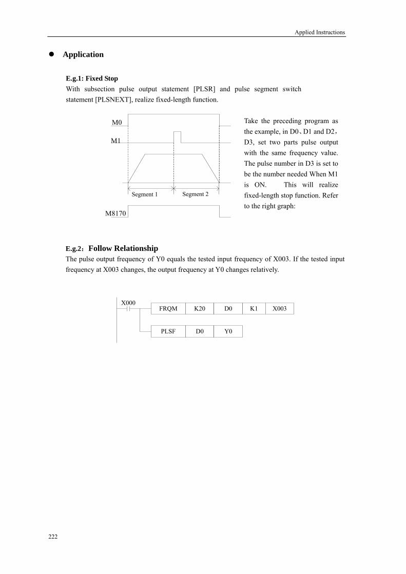
Applied Instructions
222
Application
E.g.1: Fixed Stop With subsection pulse output statement [PLSR] and pulse segment switch statement [PLSNEXT], realize fixed-length function.
M0
0
Take the preceding program as the example, in D0、D1 and D2,D3, set two parts pulse output with the same frequency value.
number in D3 is set to needed When M1
efer 2
M1
The pulsebe the number is ON. This will realize fixed-length stop function. Rto the right graph:
Segment 1 Segment
M817
FRQM KX000
20 D0 K1 X003
PLSF D0 Y0
E.g.2:Follow RelaThe pulse output frequency of Y0 equals the tested inp 3. If the tested input frequency at X003 changes, the output frequency at Y0
tionship ut frequency of X00
changes relatively.

Applied Instructions
l coil and register Som flag bits of pulse output is shown below:
ID High
frequency
pulse ID Function Description
Pulse output specia
e
M81 0 PULSE_1 Sending pulse flag Be 1 at pulse sending 7
M8171 32 bits pulse sending
Be 1 when overflow overflow flag
M81 rositive direction, the correspond
ire i N1 is p
72 Di ection flag d ction port s O
M81 3 PULSE_2 Sending pulse flag Be 1 at pulse sending 7
M81 4 32 bits pulse sending overflow flag
Be 1 when overflow 7
M8175 Direction flag 1 is positive direction, the correspond direction port is ON
M81 6 PULSE_3 Sending pulse flag Be 1 at pulse sending 7
M81 7 32 bits pulse sending overflow flag
Be 1 when overflow 7
M81 8 Di on flag 1 is positive direction, the correspond direction port is ON
7 recti
M81 9 PULSE_4 Sending pulse flag Be 1 at pulse sending 7
M81 0 32 bits pulse sending overflow flag
Be 1 when overflow 0 32 bits pulse sending overflow flag
Be 1 when overflow 8
M8181 Direction flag is positive direction, the correspond ec n p t is
1 dir tio or ON
223
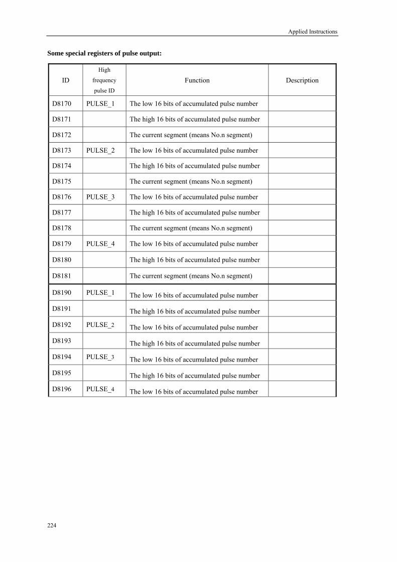
Applied Instructions
224
Some special registers of puls
High
frequency
pulse ID Function Description
e output:
ID
D8170 PULSE_1 The low 16 bits of accumulated pulse number
D8171 The high 16 bits of accumulated pulse number
D8172 The current segment (means No.n segment)
D8173 PULSE_2 The low 16 bits of accumulated pulse number
D8174 The high 16 bits of accumulated pulse number
D8175 The current segment (means No.n segment)
D8176 PULSE_3 The low 16 bits of accumulated pulse number
D8177 The high 16 bits of accumulated pulse number
D8178 ent segment (mean .n segment) The curr s No
D8179 PULSE_4 The low 16 bits of accumulated pulse number
D8180 The high 16 bits of accumulated pulse number
D8181 The current segment (means No.n segment)
D8 ULSE_1 The low 16 bits of accumulated pulse number 190 P
D8191 its of accumulated pulse number The high 16 b
D8192 PULSE_2 6 bits of accumulated pulse number The low 1
D8193 high 16 bits of umulate ulse number The acc d p
D8194 PULSE_3 low 16 bits of umu ulsThe acc lated p e number
D8195 The high 16 bits of accumulated pulse number
D8196 PULSE_4 The low 16 bits of accumulated pulse number
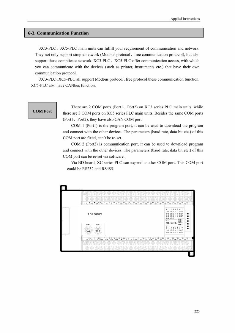
Applied Instructions
6-3. Communication Function
Y
X
X0X1COM
COM X2X3
X4X5
X6X7
X10X11
X12X13
X14X15
X16X17
X20X21
X22X23
X24X25
X26X27
X30X37
X40X36X35
X34X33
X32X31 X41
X42X43
Y27Y26
Y25Y24
Y15Y17
COM6Y21
Y20COM7
Y23Y22Y16
Y13Y14COM5
Y11Y12
Y7Y10
Y6COM4
Y4Y5
COM3Y3
Y2Y1COM2
Y0COM1COM0
CAN+CAN-
AB0V
24V
PORT2PORT1XC5-60R-E
ERRRUNPWR
0 1 32 6 754
4 5 762 310
COM Port
XC3-PLC、XC5-PLC main units can fulfill your requirement of communication and network. hey not only support simple network (Modbus protocol、free communication protocol), but also
support those complicate network. XC3-PLC、XC5-PLC offer communication access, with which ith the devices (such as printer, instruments etc.) that have their own
communication protocol. XC3-PLC、XC5-PLC all support Modbus protocol、free protocol these communication function, XC5-PLC also have CANbus function.
There are 2 COM ports (Port1、Port2) on XC3 series PLC main units, while there are 3 COM ports on XC5 series PLC main units. Besides the same COM ports (Port1、Port2), they have also CAN COM port.
COM 1 (Port1) is the program port, it can be used to download the program and connect with the other devices. The parameters (baud rate, data bit etc.) of this COM port are fixed, can’t be re-set.
COM 2 (Port2) is communication port, it can be used to download program and connect with the other devices. The parameters (baud rate, data bit etc.) of this COM port can be re-set via software.
Via BD board, XC series PLC can expend another COM port. This COM port could be RS232 and RS485.
T
you can communicate w
225

Applied Instructions
1、 RS232 COM port
备注
The pin graph of COM 1(Port1):
3 4 5
1 2
6 87
Mini Din 8 core socket (Hole)
2:PRG 4:RxD 5:TxD 6:VCC 8:GND
The pin graph of COM 1(Port1):
3 4 5
1 2
6 87
Mini Din 8 core socket (Hole)
4:RxD 5:TxD 8:GND
226

Special Functions
3
2, RS485 COM Port
3, CAN Port
Station Modbus Station number: 1~254, 255 (FF) is free format communication
Baud Rate 300bps~115.2Kbps Data Bit 8 bits data bit, 7 bits data bit Stop Bit 2 stop bits, 1 stop bit Check Even, Odd, No check
About RS485 COM port, A is “+” signal、B is “-“ signal. On XC series PLC, COM2 (Port2) can be both RS485 and RS232, so, you can’t only use two at the same time.
CAN port can be used to realize CANbus communication. please refer to“6-8.CAN bus function
(XC5 series)” For the detailed CAN communication function,
Communication Parameter
The defaulted parameters of COM 1: Station number is 1、baud rate is 19200bps、8 data bit、1 stop bit、Even check
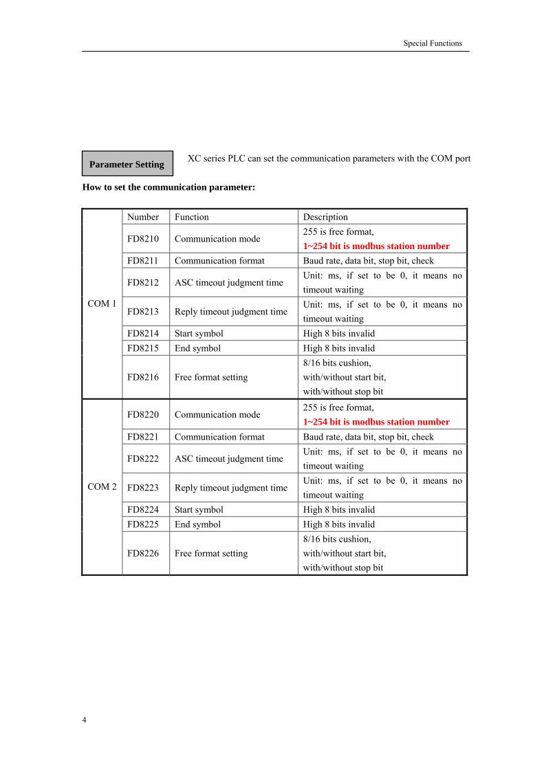
Special Functions
Number Function Description
Parameter Setting XC series PLC can set the communication parameters with the COM port
How to set the communication parameter:
FD8210 Communication mode 255 is free format,
modbus station number 1~254 bit is FD8211 Communication format Baud rate, data bit, stop bit, check
FD8212 ASC timeout judgment time Unit: ms, if timeout wait
set to be 0, it means no ing
FD8213 Reply timeout judgment time Unit: ms, if timeout wait
set to be 0, it means no ing
FD8214 Start symbol High 8 bits invalid FD8215 End symbol High 8 bits invalid
COM 1
FD8216 Free format setting hion,
with/without start bit, with/without stop bit
8/16 bits cus
FD8220 Communication mode 255 is free format, 1~254 bit is modbus station number
FD8221 Communication format Baud rate, data bit, stop bit, check
FD8222 ASC timeout judgment time Unit: ms, if set to be 0, it means no timeout waiting
FD8223 Reply timeout judgment time Unit: ms, if set to be 0, it means no timeout waiting
FD8224 Start symbol High 8 bits invalid FD8225 End symbol High 8 bits invalid
COM 2
FD8226 Free format setting 8/16 bits cushion, with/without start bit, with/without stop bit
4

Special Functions
0:300bps 1:600bps 2:1200 bps 3:2400 bps 4:4800 bps 5:9600 bps 6:19.2K bps 7:38.4K bps 8:57.6K bps 9:115.2K bps
0:8bits data 1:7bits data
0:2 stop bits 2:1stop bit
0:No check 1:Odd check 2:Even check
0:8 bits communication 1:16 bits communication
0: without start symbol 1: with start symbol
0:without end symbol 1:with end symbol
Reserve
FD8211(COM1)/FD8221(COM2):
FD8216(COM1)/FD8226(COM2):
5 14 13 12 11 10 9 8 7 6 5 4 3 2 1 0
1
15 14 13 12 11 10 9 8 7 6 5 4 3 2 1 0
Setting method of communication parameters:
5

Special Functions
6-3-1. MODBUS Communication function
Coil space: Coil’s
(Dec.) X0 Y0 S0 M8000 T0 C0
start ID M0
Corresponded Modbus ID (Hex.)
0 4000 4800 5000 6000 6400 6C00
Note: coil’s Modbus ID=Modbus ID which corresponds with coil’s start ID +coil
umber
Register space:
Register’s start ID (Dec.)
D0 TD0 CD0 D8000 FD0 FD8000
n
Corresponded Modbus ID (Hex.)
0 3000 3800 4000 4800 6800
Note: register’s Modbus ID=Modbus ID which corresponds with register’s start ID + register number
Communication
Function XC series PLC support both Modbus master and Modbus slave Master format: When PLC is set to be master, PLC sends request to other
slave devices via Modbus instructions, other devices response the master.
Slave format: when PLC is set to be slave, it can only response with other master devices.
The defaulted status of XC-PLC is Modbus slave.
Communication
ID
For the soft unit’s number in PLC which corresponds with Modbus address number, please see the following table:
6

Special Functions
1, Coil Read [COLR]
COLR K1 K500 K3 M1X0
K2
S1· S2· S3· D1· D2·
2, Coil’s Read [INPR]
Communication Instructions
Coil read instruction, Modbus function code is 01H . Function: Read ned bureau’s assigned coil status to PLC’s assigned coil.
Far away com ion bureau number . Operands: K、TD、CD、D、FD Far away coi number. Operands: K、TD、CD、D、FD Coil numb Operands: K、TD、CD、D、FD Local recei start ID. Operands: X、Y、M、S、T、C Port numb d: K1~K2 D2·
D1·
S3·
S2·
S1·
the assigmunicat
l’s start er. ve coil’s
er. Boun
Input
INPR K1 K500 K3 M1X0
K2
S1· S2· S3· D1· D2·
Instruction description: when X0 is ON, execute COLR or INPR instruction. After finish executing the instruction, set communication finish bit. No operation when X0 is OFF. If communication errors, resend automatically. If reach 10 times, set communication error flag. User can check the relative register to judge the reason.
Read the input coil instruction, Modbus function code is 02H Function: Read the assigned bureau’s assigned input coil status to PLC’s assigned coil.
Far away communication bureau number . Operands: K、TD、CD、D、FD Far away coil’s start number. Operands: K、TD、CD、D、FD Coil number. Operands: K、TD、CD、D、FD Local receive coil’s start ID. Operands: X、Y、M、S、T、C Port number. Bound: K1~K2 D2·
D1·
S3·
S2·
S1·
7
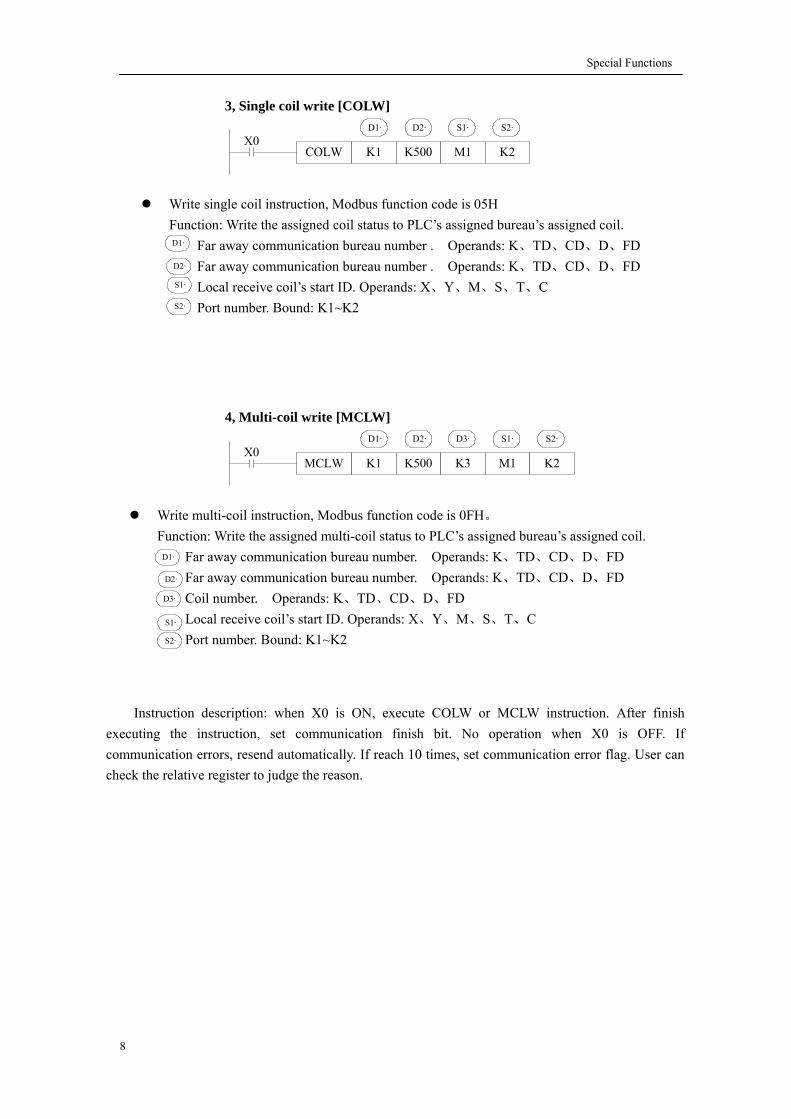
Special Functions
3, Single coil write [COLW]
COLW K1 K500 M1X0
K2
D1· D2· S1· S2·
4, Multi-coil write [MCLW]
MCLW K1 K500 K3 M1X0
K2
D1· S1· S2·D2· D3·
Write single coil instruction, Modbus function code is 05H Function: Write the assigned coil status to PLC’s assigned bureau’s assigned coil.
Far away communication bureau number . Operands: K、TD、CD、D、FD Far away communication bureau number . Operands: K、TD、CD、D、FD Local receive coil’s start ID. Operands: X、Y、M、S、T、C Port number. Bound: K1~K2
D1·
D2·
S1·
S2·
Instruction description: when X0 is ON, execute COLW or MCLW instruction. After finish executing the instruction, set communication finish bit. No operation when X0 is OFF. If communication errors, resend automatically. If reach 10 times, set communication error flag. User can check the relative register to judge the reason.
Write multi-coil instruction, Modbus function code is 0FH。
number. Operands: K、TD、CD、D、FD number. Operands: K、TD、CD、D、FD
Function: Write the assigned multi-coil status to PLC’s assigned bureau’s assigned coil. Far away communication bureau Far away communication bureau
D1·
D2·
Coil number. Operands: K、TD、CD、D、FD Local receive coil’s start ID. Operands: X、Y、M、S、T、C Port number. Bound: K1~K2
D3·
S1·
S2·
8
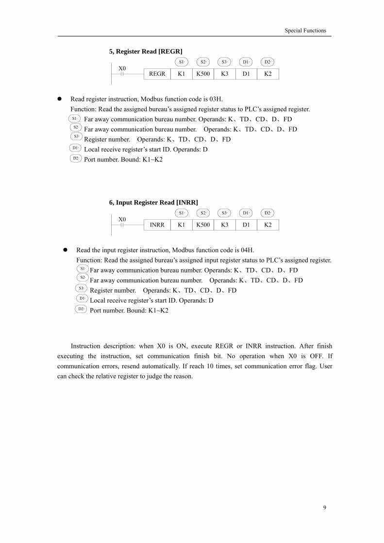
Special Functions
5, Register Read [REGR]
REGR K1 K500 K3 D1X0
K2
S1· S2· S3· D1· D2·
6, Input Register Read [INRR]
INRR K1 K500 K3 D1X0
K2
S1· S2· S3· D1· D2·
Read register instruction, Modbus function code is 03H. Function: Read the assigned bureau’s assigned register status to PLC’s assigned register.
Far away communication bureau number. Operands: K、TD、CD、D、FD Far away communication bureau number. Operands: K、TD、CD、D、FD Register number. Operands: K、TD、CD、D、FD Local receive register’s start ID. Operands: D Port number. Bound: K1~K2
S1·
S2·
S3·
D1·
D2·
Instruction description: when X0 is ON, execute REGR or INRR instruction. After finish executing the instruction, set communication finish bit. No operation when X0 is OFF. If communication errors, resend automatically. If reach 10 times, set communication error flag. User can check the relative register to judge the reason.
e is 04H. Function: Read the assigned bureau’s assigned input register status to PLC’s assigned register.
Far away communication bureau number. Operands: K、TD、CD、D、FD Far away communication bureau number. Operands: K、TD、CD、D、FD Register number. Operands: K、TD、CD、D、FD Local receive register’s start ID. Operands: D Port number. Bound: K1~K2
Read the input register instruction, Modbus function cod
S1·
S2·
S3·
D1·
D2·
9

Special Functions
7, Single Register Write [REGW]
REGW K1 K500 D1X0
K2
D1· S1· S2·D2·
8, Multi-register Write [MRGW]
MRGW K1 K500 K3 D1X0
K2
D1· D2· D3· S1· S2·
Write single register instruction, Modbus function code is 06H Function: write the assigned register status to PLC’s assigned bureau’s assigned register.
Far away communication bureau number. Operands: K、TD、CD、D、FD Far away communication bureau number. Operands: K、TD、CD、D、FD Local receive register’s start ID. Operands: D Port number. Bound: K1~K2 S2·
S1·
D2·
D1·
Instruction description: when X0 is ON, execute REGW or MRGW instruction. After finish executing the instruction, set communication finish bit. No operation when X0 is OFF. If communication errors, resend automatically. If reach 10 times, set communication error flag. User can check the relative register to judge the reason.
Write multi-register instruction, Modbus function code is 10H Function: write the assigned input register status to PLC’s assigned bureau’s assigned register.
Far away communication bureau number. Operands: K、TD、CD、D、FD Far away communication bureau number. Operands: K、TD、CD、D、FD Register number. Operands: K、TD、CD、D、FD Local receive register’s start ID. Operands: D Port number. Bound: K1~K2
S1·
S2·
S3·
D1·
D2·
10

Special Functions
6-3-2. Free Format Communication
Communication Mode:
Free Communication
Start Symbol (1 byte) Data Block (max. 128 bytes) End Symbol (1 byte)
Baud Rate: 300bps~115.2Kbps Data Format
Data Bit: 7bits、8bits Check Bit: Odd、Even、No Check Stop bit: 1 bit、2 bits
Start Symbol: 1 bit End Symbol: 1 bit User can set a start/end symbol, after set start/end symbol, PLC will automatically add this start/end symbol when sending data; remove this start/end symbol when receiving data.
Communication Format: 8 bits、16 bits If choose 8 bits cushion format to communicate, in the communication process, the high bytes are invalid, PLC only use the low bytes to send and receive data.
Free format communi ta in the format of data bloc can transfer 128 bytes at mo eanwh n set a sta ol and end sym ot set.
cation transfer daile e ck ca
k, each block st. M ach blo rt symb bol, or n
11

Special Functions
Instruction Format
1, Send Data:
SEND D10 D100 K1
S1· S2· nM0
Data sending instruction, send data every rising edge of M0 Start address of send data. Operands: K、TD、CD、D、FD The sent character’s number. Operands: K、TD、CD、D、FD
n:COM port Bound: K1~K2 In the data sending process, “sending” flag M8122 (COM 1) sets ON.
S2·
S1·
2, Receive Data:
RCV D20 D200 K1
S1· S2· nM1
Data receiving instruction, receive data every rising edge of M0 Receive address of send data. Operands: K、TD、CD、D、FD The received character’s number. Operands: K、TD、CD、D、FD
n:COM port Bound: K1~K2 In the data receiving process, “receiving” flag M8124 (COM 1) sets ON.
S2·
S1·
12
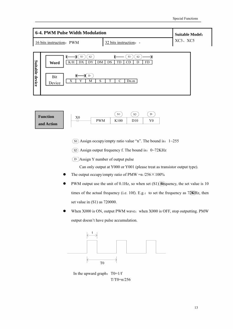
Special Functions
6-4. PWM Pulse Width Modulation
PWM K100 D10 Y0X0
S1· S2· D·
T0
t
Function
and Action
Assign occupy/empty ratio value “n”. The bound is:1~255
Assign output frequency f. The bound is:0~72KHz
Assign Y number of output pulse
Can only output at Y000 or Y001 (please treat as transistor output type).
The output occupy/empty ratio of PMW =n /256×100%
PWM output use the unit of 0.1Hz, so when set (S1) frequency, the set value is 10
times of the actual frequency (i.e. 10f). E.g.:to set the frequency as 72KHz, then
set value in (S1) as 720000.
When X000 is ON, output PWM wave;when X000 is OFF, stop outputting. PMW
output doesn’t have pulse accumulation.
S2·
D·
S1·
S2·
S2·
In the upward graph:T0=1/f T/T0=n/256
16 bits instruction:PWM 32 bits instruction:-
Suitable Model: XC3、XC5
Suitable device
Word
X Y M S T C Dn.mD·
D FDDMDX DY DS TD CDK/HS2·S1· S2·S1·
Device Bit
13

Special Functions
6-5. Frequency g
Testin
Function and Action
16 bits instruction: 32 bits instructionFRQM -
Suitable Model: XC3、XC5
Suitable device
Word Device
Bit Device X Y M S T C Dn.m
S3·
D FDDM
FRQM K20 D100 K1 X003X000
D·S1· S2· S3·
S1: Pulse cycle number (The sampled pulse cycle number in one scan cycle.)
perands: D, CD, TD
D: Testing result. Operands: D, CD, TD
S2: Frequency division choice. Bound: K1 or K2;
Whe 1, the bound is: no less than 9Hz, precision bound: 9~18KHz. When the frequency division is K2, the bound: no less than 300Hz, precision bound: 300~400KHz。
S3: pulse input X number
In frequency testing, if choose frequency division as K2, the frequency testing precision is
O
n the frequency division is K
higher than frequency division K1.
When X000 is ON, FRQM will test 20 pulse cycles from X003 every scan cycle. Calculate
the frequency’s value and save into D100. Test repeatedly. If the tested frequency’s value is
smaller than the test bound, then return the test value as 0.
DX DY DS TD CDK/HS1·S2·
D·
S1·
The correspond X number with the pulse output of frequency testing: Model X 14 points X2、X3 24/32 points X1、X11、X12 XC3 series 48/60 points X4、X5 32 points X3
XC5 series 48/60 points X1、X11、X12
14
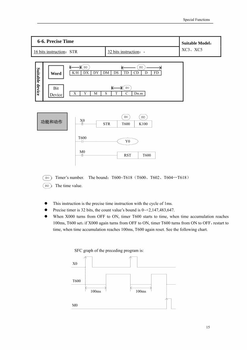
Special Functions
15
-6. Precise Time
6
16 bits instruction:STR 32 bits instruction:-
Suitable Model: XC3、XC5
Suitable device
Word
Bit Device
D1·
D FDDMDX DY DS TD CDK/HD2·D2·
X Y M S T C Dn.m
STR T600 K100X0
D1· D2·
Y0T600
RST T600M0
SFC graph of the preceding program is:
功能和动作
:Timer’s number. The bound:T600~T618(T600、T602、T604…T618)
:The time value.
This instruction is the precise time instruction with the cycle of 1ms.
ON, timer T600 starts to time, when time accumulation reaches 100ms, T600 set;if X000 again turns from OFF to ON, timer T600 turns from ON to OFF,restart to time, when time accumulation reaches 100ms, T600 again reset. See the following chart.
D1·
D2·
Precise timer is 32 bits, the count value’s bound is 0~+2,147,483,647. When X000 turns from OFF to
X0
T600
100ms 100ms
M0
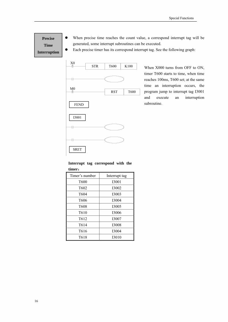
Special Functions
When precise time reaches the count value, a correspond interrupt tag will be
upt tag. See the following graph:
Precise generated, some interrupt subroutines can be executed.
Each precise timer has its correspond interr
STR T600 K100X0
RST T600M0
I3001
SRET
FEND
Interrupt tag correspond with the timer: Timer’s number Interrupt tag
Ti
Int
timer T600 starts to time, when time reaches 100ms, T600 set; at the same time an interruption occurs, the program jump to interrupt tag I3001 and execute an interruption subroutine.
me
erruption
When X000 turns from OFF to ON,
T600 I3001 T602 I3002 T604 I3003 T606 I3004 T608 I3005 T610 I3006 T612 I3007 T614 I3008 T616 I3004 T618 I3010
16

Special Functions
17

Special Functions
6-7.C all have interrupt function. There are two kinds of interrupt function: external
errupt function, some special program can be disposed, not affecte
6-7-1.External Interrupt Inpuwith an eternal in
correspond interrupt sumain program.
Interruption Function XC series PL
interrupt and time interrupt. Via intd by PLC’s scan cycle.
t terminal X can be used as external interrupt’s input, each input terminal corresponds terrupt, the rising edge or falling edge of each input can both active the interrupt.
The interrupt subroutine is written behind the main program (Behind FEND command). When interrupt activates, the main program will immediately stop executing, turn to execute the
broutine. After finish executing the interrupt subroutine, go on execute the
Definition of external interrupt port:
XC3-14 models Pointer’s tag
Input
terminal Rising interrupt Falling interrupt Forbid interrupt
instruction X7 I0000 I0001 M8050
XC3-24/32 models, XP-18 and XC5-48/60 models
Pointer’s tag Input terminal Rising interrupt Falling interrupt
Forbid interrupt instruction
X2 I0000 I0001 M8050 X5 I0100 I0101 M8051
X10 I0201 52 I0200 M80
XC3-48/60 mnter’s t
odels Poi ag Input
terminal Rising interrupt
Falling interrupt instruction Forbid interrupt
X11 I0001 50 I0000 M80X10 I0100 I0101 M8051 X7 I0200 I0201 M8052
Interrupt Instructio
Main program Main program
Interrupt subroutine
Input interruption
n
18
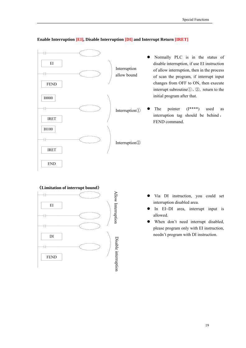
Special Functions
Enable Interruption [EI], Disable Interruption [DI] and Interrupt Return [IRET]
EI
FEND
I0000
IRET
I0100
IRET
END
Limitation of interrupt bound》
《
EI
FEND
DI
Interruption allow bound
Interruption①
Interruption②
Normally PLC is in the status of disable interruption, if use EI instruction
ption, then in the process of scan the program, if interrupt input changes from OFF to ON, then execute int subroutine①、②, return to the initial program after that.
The pointer (I****) used as interruption tag should be behind , FEND command.
of allow interru
errupt
Disable interruption
Via DI instruction, you could set interruption disabled area.
In EI~DI area, interrupt input is allowed.
When don’t need interrupt disabled, please program only with EI instruction, needn’t program with DI instruction.
Allow
Interruption
19

Special Functions
《Disable Interruptio
n》
EI
M8050
FEND
I0000
IRET
END
Enable interruption Interrupt Subroutine
To each input interruption, special relay of disable interruption is given. (M8050~M8052)
In the left program, if use M0 to make
M8050 “ON”, then disable the interrupt input of route 0
M0
20

Special Functions
6-7-2.Time Inte
rrupt
Y0
FEND
I4010
INC D0
IRET
X0
M8000
Table of interruption tag:
Interruption tag Disable interruption struction
Description
in
Function
and Action
ro le too long, if certain special program should be executed; or should be executed every certain time, t unction is suitable. It could be not affected by PLC’s scan cycle, execute the time interrupt program every Nms.
efaulted time inter open. Time interrupt subroutine is similar with other interru t must be written behind the main program, start with I40xx IRET.
There are 10 routes time 9**. (** e, the unit is ms.)E.g. I4010 means execute the first
route’s interruption every 10ms.
In the condition of the main p gram’s executing cycin sequential control scan, a special programime interruption f
The d ruption status ispt subroutines. I
instruction, end with interruption, the denote method is: I40**~I4
means time interrupt’s tim
I40** M8056
I41** M8057
I42** M8058
I43** - I44** - I45** - I46** - I47** - I48** - I49** -
“**” denotes the time of time interrupt. The bound is 1~99, unit is “ms”.
21
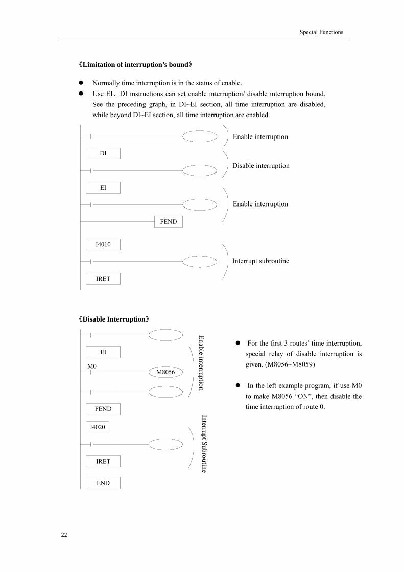
Special Functions
《Limitation of interruption’s bound》
FEND
I4010
IRET
DI
EI
《Disable Interruption》
EI
M8056
FEND
I4020
IRET
END
M0
Normally time interruption is in the status of enable. Use EI、DI instructions can set enable interruption/ disable interruption bound.
See the preceding graph, in DI~EI section, all time interruption are disabled, while beyond DI~EI section, all time interruption are enabled.
Enable interruption
Enable interruption
Disable interruption
Interrupt subroutine
Enable interruption Interrupt Subroutine
For the first 3 routes’ time interruption, special relay of disable interruption is given. (M8056~M8059)
In the left example program, if use M0
to make M8056 “ON”, then disable the time interruption of route 0.
22

Special Functions
CAN-Bus Brief Introduction
6-8. CAN-Bus Function(XC5 Series)
CAN: Controller Area Network, included in industrial area bus category. Compared with
common communication bus, CAN bus data communication has performance of outstanding dependability, real time ability and flexibility.
CAN controller works under multi-master format. In the network, each node can send data to bus according to the bus visit priority. These characters make each node in CAN bus network has stronger data communication real time performance, and easy to construct redundant structure, improve the system’s dependability and flexibility.
In CANBUS network, any node can initiatively send message at any time to any other node, no master and no slave. Flexibility communication, it’s easy to compose multi-device backup system, distributing format monitor, control system. To fulfill different real time requirement, the nodes can be divided to be different priority level. With non-destroy bus arbitrament technology, when two nodes send message to the network at the same time, the low level priority node initiatively stop data sending, while high level priority node can continue transferring data without any influence. So there is function of node to node, node to multi-node, bureau broadcasting sending/receiving data. Each frame’s valid byte number is 8, so the transfer time is short, the probability ratio is low.
External Connection
CAN-Bus Communication Port: CAN+, CAN- The connection among each node of CAN bus is shown in the following, at the two ends, add 120 ohm middle-terminal resistors.
CAN-bus Node Sub-address 01
CAN-bus Node Sub-address 02
CAN-bus Node Sub-address 03
CAN-bus Node Sub-address 04
Sub-address 00
120R 120R
120R 120R
00 01 02
23
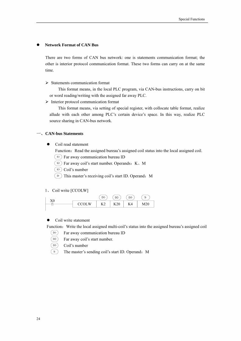
Special Functions
Network Format of CAN Bus
There are two forms of CAN bus network: one is statements communication format; the
e.
N-bus instructions, carry on bit
o d far away PLC.
ble format, realize a ertain device’s space. In this way, realize PLC s
CA 1、 Coil write [CCOLW]
other is interior protocol communication format. These two forms can carry on at the same tim
Statements communication format This format means, in the local PLC program, via CA
r word reading/writing with the assigneInterior protocol communication format
This format means, via setting of special register, with collocate tallude with each other among PLC’s cource sharing in CAN-bus network.
一、 N-bus Statements
CCOLW K2 M20K20 K4X0
S·D1· D2· D3·
Coil read statement Function:Read the assigned bureau’s assigned coil status into the local assigned coil.
Far away communication bureau ID Far away coil’s start number. Operands:K、M Coil’s number This master’s receiving coil’s start ID. Operand:M
Coil write statement Function:Write the local assigned multi-coil’s status into the assigned bureau’s assigned coil
Far away communication bureau ID Far away coil’s start number. Coil’s number The master’s sending coil’s start ID. Operand:M
S·
D3·
D2·
D1·
D·
S3·
S2·
S1·
24

Special Functions
25
2、 Register read [CREGR]
CREGR K2 D20K20 K4
S1· S2· S3· D·X0
3、 Register write [CREGW]
CREGW K2 D20K20 K4X0
S·D1· D2· D3·
ter statement Function:Read the assigned bureau’s assigned register to the local assigned register.
Far away communication bureau ID. Far away register’s start number. Operands:K、D Register number.
rand:D
Read regis
S1·
S2·
S3·
Local receiving register’s start ID. OpeD·
Write register statement
the local assigned input register into the assigned bureau’s assigned register.
cal receiving register’s start ID. Operand:D
Function:Write Far away communication bureau ID. Far away register’s start number. Register number. Lo
D1·
D2·
D3·
S·

Special Functions
Interior protocol communication format
Function description: Open and close of interior protocol communication function
r FD8350:
is defaulted closed. Communication parameters setting
Setting frequency these parameters are shown below:
Defini Interior protocol communicates via setting configure items. There s: read bit’s item, read word’s item, write bit’s item, write
word’s ite
Add separately four configure item’s number: FD8360—read bit’s item, ’s
Step 2, configure each item’s communication object, each item needs to set four parameters: according to the order: far away node’s bureau ID, far away node’s object ID, local object’s ID, number. The correspond register ID: FD8370~FD8373 means item 1, FD8374~FD8377 means item 2, … …
FD9390~FD9393 means item 256;totally 256 configure items can be set.
Using via setting the data of registe0 means not use CAN interior protocol communication;1 means use CAN interior protocol communication CAN interior protocol communication function
of baud rate, bureau ID, and sending
tion of configure items
are four configure itemm.
Configure format: Step 1,
FD8361—read word’s item, FD8362—write bit’s item, FD8363—write worditem.
26

Special Functions
CAN Communication Setting
ID Function Description
FD8350 CAN communication mode 0 means not use;1 means interior protocol FD8351 CAN baud rate Refer to CAN baud rate setting table FD8352 Self’s CAN bureau ID CAN protocol using (the defaulted value is 1)
FD8354 Configured sending
frequency
The set value’s unit is ms (sending one time every several ms)
Set to be 0 means sending every cycle, the defaulted value is 5ms
FD8360 Read bit’s item FD8361 Read word’s item FD8362 Write bit’s item FD8363 Write word’s item
-
FD8370 Far away node ID FD8371 Far away node’s object ID FD8372 The local object’s ID FD8373 number
Item 1 configure
…… …… …… FD9390 Far away node ID FD9391 Far away node’s object ID FD9392 Local object’s ID FD9393 Number
Item 256 configure
27

Special Functions
CAN baud rate setting table:
FD8351 setting value
Baud rate(BPS)
0 1K 1 2K 2 5K 3 10K 4 20K 5 40K 6 50K 7 80K 8 100K 9 150K
10 200K 11 250K 12 300K 13 400K 14 500K 15 600K 16 800K 17 1000K
CAN node status: M8350 Configure item 1 M8351 Configure item 2 M8352 Configure item 3 M8353 Configure item 4 M8354 Configure item 5 M8355 Configure item 6 M8356 Configure item 7 M8357 Configure item 8 M8358 Configure item 9 : M8605 Configure item 256
Reset after receiving confirmation
28
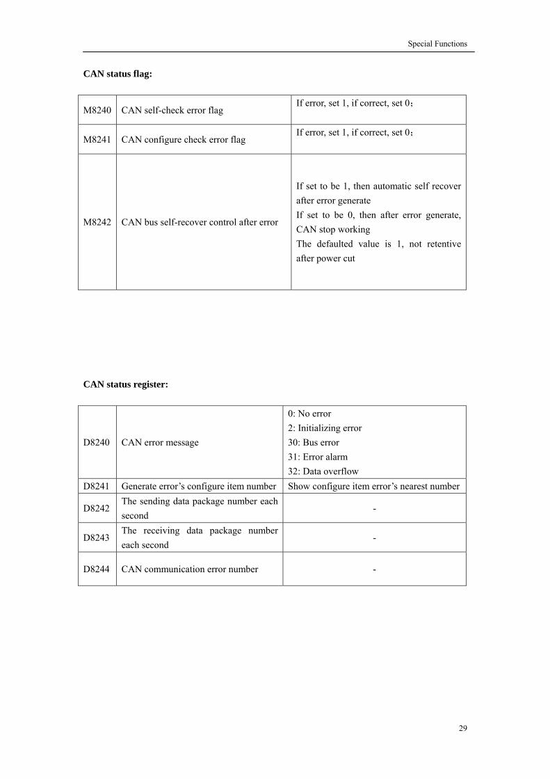
Special Functions
CAN status flag:
8240 CAN self-check error flag If error, set 1, if correct, set 0;
M
M8241 CAN configure check error flag If error, set 1, if correct, set 0;
M8242 CAN bus self-recover control after error
If set to be 1, then automatic self recover after error generate If set to be 0, then after error generate, CAN stop working The defaulted value is 1, not retentive after power cut
CAN status register:
D8240 CAN error message
0: No error 2: Initializing error 30: Bus error 31: Error alarm 32: Data overflow
D8241 Generate error’s configure item number Show configure item error’s nearest number
D8242 The sending data package number each second
-
D8243 The receiving data package number each second
-
D8244 CAN communication error number -
29

Special Functions
In this chapter, we give you some sample programs for your reference.
XC series PLC is mini model、high speed、good performance PLC. Besides the independent using of I/O points,
pulse output and other functions could be used. So XC series PLC could satisfy diverse control.
7. Applied Example Programs
7-1.Example of Pulse Output
7-2.Example of MODBUS Instructions
7-3.Example of Free Format Communication
30

Special Functions
7-1. Example of Pulse Output
E.g: The following is the program which realize continuous sending high-low pulse parameters:
rs o 8 degree/step, fractionlet =40, the pulse number of a round is 8000。
High frequen Hz, the total pulse number is 24000(3 rounds) uen ax frequency 10KHz, total pulse number is 8000(1 round)
Ladder program:
The Paramete f step motor: step square angle =1.
cy pulse: max frequency is 100Kcy pulse: MLow freq
tatement Program: D M8002 //Initially forth pulse coil ET M0 //Set M0 ON DF M10 //M10 falling edge trigger condition
DMOV K100000 D200 //Transfer decimal data 100000 into double-word register D200
DMOV K24000 D210 // Transfer decimal data 24000 into double-word register
SLSL
31

Special Functions
D210 MOV K100 D220 // Transfer decimal data 10 ster D220 L //M10 igger condition D // Tra l data 10000 into double-word register D200 D K // Tra l data 8000 into double-word register D210 LD M1 //M1 status trigger condition OUT T //100m ds LD T //T0 staSET M1 //set M1 SET M // set MLDF M //M817 ition RST M0 //reset M0 RST M // reset MALT M //M10 sLD M0 //M0 status trigger condition DPLSR D200 D210 D220 Y0 //Take value is D200 as frequency, value in D210 as
pulse number, value in D220 as speedup/speed-down time, send pulse via Y0
0 into word regiDP M10 rising edge trMOV K10000 D200 nsfer decima
MOV 8000 D210 nsfer decima
0 K20 s counter T0, time 2 secon0 tus trigger condition
0 1 8170 0 falling edge trigger cond
1 1 10 tatus reverse
Program description: When PLC changes from STOP to RUN, M8002 coil gets through a scan cycle, set high
ncy t ed-down time into D220, set M0, tor uency and work 3 rounds, set coil M8170 at the same
time; the motor runs 3 rounds, the speed-down till stop, coil M8170 reset. Here reset M0, set M1, revers quency parameters into D200、D210. the counter starts to delay with 2 seconds, when reach this 2 seconds, M1 is reset, M0 is set again, the motor starts to run 1 round with low frequency. After finish this 1 round, the motor starts to run with high
again! In this format, the motor runs with high frequency and low frequency.
frequethe mo
pulse parameters into D200、D210, se speedup/spestart to speedup with high freq
e M10 status, set low fre
frequency
32

Special Functions
7-2. Example of MODBUS Instructions E.g.: The following is the communication program of one master station and 4 slave stations Each parT er s ation2: Ladder program:
ameters: he mast tation number is 1, slave st s numbers are 2, 3, 4, 5. This example, we use COM
33
Program description: When PLC changes from STOP to RUN, M8002 coil gets through a scan cycle. S0 flow
open, write master machine’s D10——D14 into No.2 slave machine’s D10——D14. after finish communication, set M8138, at the same time write slave machine’s D15——D19 into master machine’s D15——D19,set communication finish flag. Realize write and read to a slave station. At this time flow S3 will judge with the slave station. If the station number is less than 5,station number add 1,offset add 10;or else station number starts from number 2 station again.

Special Functions
7-3. Example of free format communication This example is the free format program with DH107/DH108 series instruments: I, Interface specification DH107/DH108 series instruments use asynchronism serial communication ports, the interface level fits the standard of RS232C or RS485. the data format is 1 start bit, 8 bits data, no check bit, one or two stop bits. Baud rate of communication transfer data could modified to be
200~19200bit/s
II, Format of communication instructions DH107/108 instruments use Hex. data format to indicate each instruction code and data. Rea ite instruction:R he a ameter’s (to read) code+0+0+CRC check code W he address code +43H(67)+ parameter’s (to write) code +the write data’s low byte
write eck code R ruc rameter’s (To read) code *256+82+ADDR ADDR is instrument’s ID value, the bounr nt ca ceding data operate with binary 16 bits i us. low byte is ahead, the high byte is behind W truction’s CRC check code is: parameter’s (to write) code *256+67+parameter’s (to write) value T et ted N write or read, the instruments willThe test va e Sr ten checP and the read parameter’s value sho ach engrosses 2 bytes, MV engr ne byte, the data bound is 0~220, t one byte, CRC check code ngross 2 bytes, the total is 10 bytes.
CRC check code is PV+SV+(alarm status *256+MV)+parameter’s value +ADDR, the redundant caused by the integer plus
(the detailed format, please refer to AIBUS communication protocol description) .
II, Compile communication program fter power on, the program read the current temperature value every 40ms. In this period the user
ould also write the set temperature value. Data area definition: send data buffer area: D10~D19
Accept data buffer area: D20~D29 Instrument’s station ID: D30 Read command’s value: D31=52 H Write command’s value: D32=43 H Parameter’s code: D33 Temperature setting: D34 CRC check code: D36
1
d/wr ead: T ddress code +52H(82)+parrite: T+the data’s high byte +CRC ch
ead inst tion’s CRC check code is: pad is 0~100 (please do not add 80H). CRC is the on: the preedunda used by the following operati
nteger pl The redundant is 2 bytes, the rite ins
+ADDR he param er’s (to write) value is indica by Hex. binary integer
return the following data V+ the output value MV and alarm status + k code
o matterlue PV+ the given valu
ead/writ parameter’s value +CRCV, SV
osses ould be integer format, ehe alarm status engrosses
e
IAc
34

Special Functions
Temperature display: D200,D201 Form of sending d H 43H 00H c8H 00H 0c of the current t re)S co ameters: baud rate: 9600, 8 bits data bit, 2 bits stop bit, no check. Set FD8220=255;FD8221=5。 N h th the slave m gher than V2.4)
at ata: 81H 81 H 01H (displayemperatu etting of mmunication par
ote (bot e host machine and achine should use the version hi
35

Special Functions
Program:
36

Special Functions
D32: write command value
D34: temperature setting
37

Special Functions
38
Special Functions
This chapter gives some auxiliary i f XC series PLC.
8. Appendix
nformation o
8-1.List of special auxiliary relay, special data register
8-2.List of Special FLASH data register SFD
8-3 Brief Introduction of XC1 series PLC .
8-4 Brief Introdu eries PLC . ction of XC5 s
39

Special Functions
8-1. List of special auxiliary re l data register
io Description
lay, specia
ID Funct n
Special s ’s type and its function oft unit
PC status(M)
M8000 g normally
ON coiPLC be ON when
running Workin
l
M8001 Working normally
OFF coPLC be OFF when
running il
M8002 itial pospulse co
The first scan cycle is ON when PLC starts
running
In itive il
M8003 Initial negative
pulse coil
The first scan cycle is OFF when PLC starts
running
M8005 Battery voltage too
low Act when ba voltage abnormal too low ttery
ID Function Description
PC status(D)
D8002 Register’s capacity 2…2K steps;4…4K steps;8…8K steps
D8005 Battery voltage 0.1V unit
40

Special Functions
ID Function Description
M8010
5ms
M8011 Shake with the cycle of 10ms
5ms
M8012
50ms
50ms
Shake with the cycle of 100ms
M8013 Shake with the cycle of 1
0.5s
0.5s
M8014
30s
30s
Shake with the cycle of 1
M8018 Bits of year Defaulted is OFF(OFF: 2;ON: 4)
Function Description
ID
M8020 esuZero When plus/minus operation r lt is 0
M8021 Borrow s operation When borrow occurs in minu
M8022 Carry When carry occurs in plus operation or overflow occurs in bit shift operation
M8023
M8026 RAMP mode
M8029
Clock(M)
Flag (M)
41

Special Functions
ID Function Description
D8010 The curren nit: 0.1mst scan cycle U
D8011 Mini value of scan time Unit: 0.1ms
D8 x vale of 0.1ms 012 Ma scan time Unit:
D8013 Second(clock) 0~59(BCD code format)
D8014 Minute(clock) 0~59(BCD code format)
D8015 Hour(clo 3(BCD cck) 0~2 ode format)
D8016 Date(clock) 0~31(BCD code format)
D8017 Month(cloc 12(BCDk) 0~ code format)
D8018 Year(clock 2099( at) ) 2000~ BCD code form
D8 ek(clock) 0(Sunday)~ D cod019 We 6(Saturday)(BC e format)
ID scriptiFunction De on Model Low byte
D8021 Serial num Higber h byte Compatib er Lowle system’s version numb byte
D8022’s Hig
System version number h byte Compatible m ber Loodel’s version num w byte
D8023Model’s vers H
ion number igh byte
D8024
D8025
D8026
s iModel’ nformation
D8027
D8028
D8029
Suitable h
M \0”
ost machine version
ax 5 ASC and a“
Clock (D)
Flag(D)
42
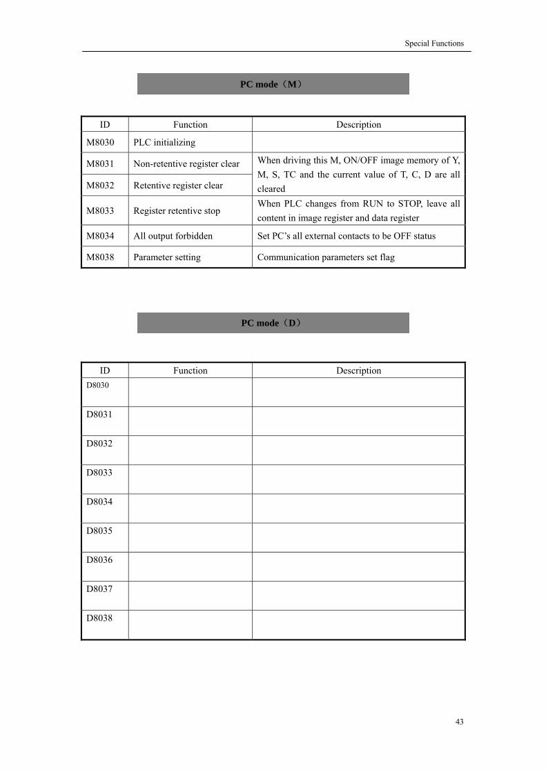
Special Functions
ID Function Description
M8030 PLC initializing
M8031 tentive register clear Non-re
M8032 register clear
When driving this , ON/OFF image memory of Y, M, S, TC and the current value of T, C, D are all cleared Retentive
M
M8033 Register re tive stop When PLC changes from RUN to STOP, leave all content in image register and data register
ten
M8034 orbidden Set PC’s all exter contacts to be OFF status All output f nal
M8038 ter setting Communication parameters set flag Parame
ID Function Description D8030
D
8031
D
8032
D8033
D8034
D8035
D8036
D8037
D80
38
PC mode(M)
PC mode(D)
43
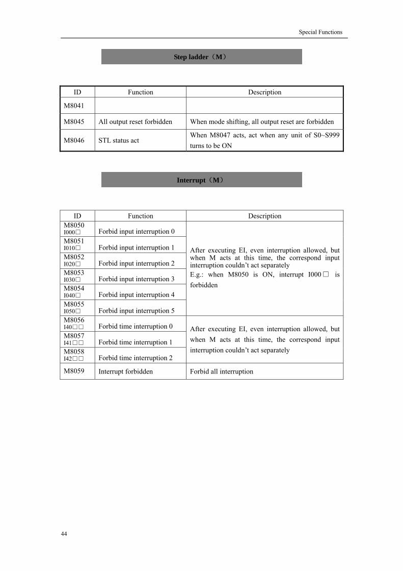
Special Functions
ID Function Description
M8041
M8045 All output reset forbidden When mode shifting, all output reset are forbidden
M8046 tturns to
STL sta us act When M8047 acts, act when any unit of S0~S999
be ON
ID
Function Description M8050 I000 d iForbi nput interruption 0 M8051 I010 d input interruption 1 ForbiM8052 I020 d iForbi nput interruption 2 M8053 I030 d i ption 3 Forbi nput interruM8054 I040 d i ption 4 Forbi nput interruM8055 I050 Forbid input interruption 5
After e tion allowed, but acts at this time, the correspond input
E.g.: when M8050 is ON, interrupt I000 is forbidd
xecuting EI, even interrupwhen Minterruption couldn’t act separately
en
M8056 I40 d tForbi ime interruption 0 M8057 I41 Forbid time interruption 1 M8058 I42 d t
After e rruption allowed, but when the correspond input interrup rately
Forbi ime interruption 2
xecuting EI, even inteM acts at this time,tion couldn’t act sepa
M8059 up Forbid all interruption Interr t forbidden
Step ladder(M)
Interrupt(M)
44

Special Functions
ID Function Description
M8067 Operation error Power on and STOP->RUN check
M8070 Scan overtime
M8071 No user program Interior codes checking error
M8072 User program error Execute code or collocate table check error
ID Function ription Desc
D8067 Execute error c Error of divide ode’s ID
D8068 error code’s ID Lock occur
D8069
D8070 Scan time of overtime s Unit: 1m
D8074 Excursion reg ID of ister D
D8097
D8098
Error check(M)
Error check(D)
45

Special Functions
ID Function Description
M8120
M 232 is sending flag 8122 RS
M81 is receiving flag 24 RS232
M81 ive imperfect flag Receiving finished normally, but the rec s less than the required
25 Receeived data i
M8127 Receive error flag
M8128 Receive corre ct flag
COM1
M812 Timeout judgment flag 9
M8130
M8132 RS232 is sending flag
M81 S232 is receiving flag 34 R
M81 eceive imperfect flag Rec ed normally, but the
s than the required 35 R
eiving finishreceived data is les
M8137 Receive error flag
M8138 Receive correct flag
M8139 Timeout judgment flag
COM2
M8140
M8142 RS232 is sending flag
M814 RS232 is receiving flag 4
M814 Receive imperfect flag Receiving finished normally, but the recei is less than the required
5 ved data
M8147 Receive error flag
M8148 ive correct flag Rece
M814 imeout judgment flag 9 T
COM3
Co mmunication(M)
46

Special Functions
47
Function Description
ID
D8120
D8121
D8123 Data number received by RS232
D8126
D8127 Communication error code
7: hardware error 10: no start sign 8: CRC check error 11: no end sign 9: bureau ID error 12: communication time out
D8128
COM1
D8129
D8130
D8131
D8133 Data number received by RS232
D8136
D8137 Communication error code
7: hardware error 10: no start sign 8: CRC check error 11: no end sign 9: bureau ID error 12: communication time out
D8138
COM2
D8139
D8140
D8141
D8143 Data number received by RS232
D8146
D8147 Communication error code
7: hardware error 10: no start sign 8: CRC check error 11: no end sign 9: bureau ID error 12: communication time out
D8148
COM3
D8149
Communication(D)

Special Functions
ID ion Description ID
Counter Funct
M8150 C600 Count finished sign 24 segments count finished, flag is 1
M8151 C602 Count finished sign 24 segments count finished, flag is 1
M8152 C604 Count finished sign 24 segments count finished, flag is 1
M8153 C606 Count finished sign 24 segments count finished, flag is 1
M8154 C608 Count finished sign 24 segments count finished, flag is 1
M8155 Count finis ts count fin is 1 C610 hed sign 24 segmen ished, flag
M8156 C612 Count finished sign 24 segments count finished, flag is 1
M8157 Count finished sign 24 se ount finished, flag is 1 C614 gments c
M81 nt finished sign ished, flag is 1 58 C616 Cou 24 segments count fin
M8159 C618 Count finished sign 24 segments count finished, flag is 1
M8160 C620 Count finished sign count finished, flag is 1 24 segments
M8161 C622 nt finished sign count finished, flag is 1 Cou 24 segments
M8162 C624 Count finished flag is 1 sign 24 segments count finished,
M8163 C626 Count finished flag is 1 sign 24 segments count finished,
M8164 C628 Count finished sign 24 segments count finished, flag is 1
M8 C630 Count finished s flag is 1 165 ign 24 segments count finished,
M8166 C632 Count finished sign count finished, flag is 1 24 segments
M8167 C634 Count finish is 1 ed sign 24 segments count finished, flag
M8168 C636 Count finished sign 24 segments count finished, flag is 1
M8 unt finished sign 24 segments count finished, flag is 1 169 C638 Co
High speed count(M)
48

Special Functions
ositive/negative count
ID High
frequency
pulse ID Function Description
P
M8170 PULSE_1 Sending pulse flag Be 1 at pulse sending
M8171 32 bits pulse sending overflow flag
Be 1 when overflow
M8172 Direction flag 1 is positive direction, the correspond direction port is ON
M8173 PULSE_2 Sending pulse flag Be 1 at pulse sending
M8174 32 bits pulse sending overflow flag
Be 1 when overflow
M8175 Direction flag 1 is positive direction, the correspond direction port is ON
M8176 PULSE_3 Sending pulse flag Be 1 at pulse sending
M8177 32 bits pulse sending overflow flag
Be 1 when overflow
M8178 Direction flag 1 is positive direction, the correspond direction port is ON
M8179 PULSE_4 Sending pulse flag Be 1 at pulse sending
M8180 32 bits pulse sending overflow flag
Be 1 when overflow
M8181 Direction flag 1 is positive direction, the correspond direction port is ON
ID Counter’s ID Function Description
M8238 C300~C498 Control of positive/negative count
0 is plus count, 1 is minus count, the defaulted is 0
……
Pulse output(M)
49

Special Functions
50
ID Counter’s ID Function Description
D8150 C600 The current segment (means No.n segment)
D8151 C602 The current segment
D8152 C604 The current segment
D8153 C606 The current segment
D8154 C608 The current segment
D8155 C610 The current segment
D8156 C612 The current segment
D8157 C614 The current segment
D8158 C616 The current segment
D8159 C618 The current segment
D8160 C620 The current segment
D8161 C622 The current segment
D8162 C624 The current segment
D8163 C626 The current segment
D8164 C628 The current segment
D8165 C630 The current segment
D8166 C632 The current segment
D8167 C634 The current segment
D8168 C636 The current segment
D8169 C638 The current segment
High speed count(D)

Special Functions
51
ID High
frequency
pulse ID Function Description
D8170 PULSE_1 The low 16 bits of accumulated pulse number
D8171 The high 16 bits of accumulated pulse number
D8172 The current segment (means No.n segment)
D8173 PULSE_2 The low 16 bits of accumulated pulse number
D8174 The high 16 bits of accumulated pulse number
D8175 The current segment (means No.n segment)
D8176 PULSE_3 The low 16 bits of accumulated pulse number
D8177 The high 16 bits of accumulated pulse number
D8178 The current segment (means No.n segment)
D8179 PULSE_4 The low 16 bits of accumulated pulse number
D8180 The high 16 bits of accumulated pulse number
D8181 The current segment (means No.n segment)
Only XC5-32RT-E (4 pulse) have
D8190 PULSE_1 The low 16 bits of accumulated pulse number
D8191 The high 16 bits of accumulated pulse number
D8192 PULSE_2 The low 16 bits of accumulated pulse number
D8193 The high 16 bits of accumulated pulse number
D8194 PULSE_3 The low 16 bits of accumulated pulse number
D8195 The high 16 bits of accumulated pulse number
D8196 PULSE_4 The low 16 bits of accumulated pulse number
D8197 The high 16 bits of accumulated pulse number
Only XC5-32RT-E (4 pulse) have
Pulse output(D)

Special Functions
52
Unit Type ID(as register) Max
I/O//channels Input switch quantity X X100~X137 32 points
Output switch quantity Y Y100~Y137 32 points Input analog ID ID100~ID131 16 channels
Output analog QD QD100~QD131 16 channels
Expansion 1#
Module’s set value D D8250~D8259 - Input switch quantity X X200~X237 32 points
Output switch quantity Y Y200~Y237 32 points Input analog ID ID200~ID231 16 channels
Output analog QD QD200~QD231 16 channels
Expansion 2#
Module’s set value D D8260~D8269 - Input switch quantity X X300~X337 32 points
Output switch quantity Y Y300~Y337 32 points Input analog ID ID300~ID331 16 channels
Output analog QD QD300~QD331 16 channels
Expansion 3#
Module’s set value D D8270~D8279 - Input switch quantity X X400~X437 32 points
Output switch quantity Y Y400~Y437 32 points Input analog ID ID400~ID431 16 channels
Output analog QD QD400~QD431 16 channels
Expansion 4#
Module’s set value D D8280~D8289 - Input switch quantity X X500~X537 32 points
Output switch quantity Y Y500~Y537 32 points Input analog ID ID500~ID531 16 channels
Output analog QD QD500~QD531 16 channels
Expansion 5#
Module’s set value D D8290~D8299 - Input switch quantity X X600~X637 32 points
Output switch quantity Y Y600~Y637 32 points Input analog ID ID600~ID631 16 channels
Output analog QD QD600~QD631 16 channels
Expansion 6#
Module’s set value D D8300~D8309 - Input switch quantity X X700~X737 32 points
Output switch quantity Y Y700~Y737 32 points Input analog ID ID700~ID731 16 channels
Output analog QD QD700~QD731 16 channels
Expansion 7#
Module’s set value D D8310~D8319 - Input switch quantity X X1000~X1037 32 points
Output switch quantity Y Y1000~Y1037 32 points Input analog ID ID1000~ID1031 16 channels
Output analog QD QD1000~QD1031 16 channels
BD Expansion
Module’s set value D D8320~D8329 -
Expansion’s information(D)

Special Functions
53
8-2. List of special FLASH data register SFD 1、 I filter
Number Function Description FD8000 X port, input filter time value Unit: ms FD8002 FD8003 FD8004 FD8005 FD8006 FD8007 FD8008 FD8009
2、 I mapping Number Function Description FD8010 X00 corresponds with I** X0 corresponds with the number of input image I** FD8011 X01 corresponds with I** FD8012 X02 corresponds with I** …… …… FD8073 X77 corresponds with I**
3、 O mapped Number Function Description FD8074 Y00 corresponds with I** Y0 corresponds with the number of input image O** FD8075 Y01 corresponds with I** FD8076 Y02 corresponds with I** …… …… FD8137 Y77 corresponds with I**
4、 I property Number Function Description FD8138 X00 property 0: positive logic;others: negative logic FD8139 X01 property FD8140 X02 property …… …… FD8201 X77 property
5、 Device’s power failure retentive area Number Function Description FD8202 Start tag of D power failure store area FD8203 Start tag of M power failure store area FD8204 Start tag of T power failure store area FD8205 Start tag of C power failure store area FD8206 Start tag of S power failure store area

Special Functions
54
6、 Communication
Number Function Description
FD8210 Communicate mode 255 is free format, 1~254 bits modbus station ID
FD8211 Communicate format Baud rate, data bit, stop bit, checkout
FD8212 Judgment time of ASC timeout
Unit: ms
FD8213 Judgment time of reply timeout
Unit: ms, if set to be 0, it means no timeout waiting
FD8214 Start ASC High 8 bits be of no effect FD8215 End ASC Low 8 bits be of no effect
COM1
FD8216 Free format setting 8/16 bits cushion, with/without start bit, with/without end bit,
FD8220 Communicate mode 255 is free format, 1~254 bits modbus station ID
FD8221 Communicate format Baud rate, data bit, stop bit, checkout
FD8222 Judgment time of ASC timeout
High 8 bits be of no effect
FD8223 Judgment time of reply timeout
Low 8 bits be of no effect
FD8224 Start ASC Unit: ms
FD8225 End ASC Unit: ms, if set to be 0, it means no timeout waiting
COM2
FD8226 Free format setting 8/16 bits cushion, with/without start bit, with/without end bit
FD8230 Communicate mode 255 is free format, 1~254 bits modbus station ID
FD8231 Communicate format Baud rate, data bit, stop bit, checkout
FD8232 Judgment time of ASC timeout
High 8 bits be of no effect
FD8233 Judgment time of reply timeout
Low 8 bits be of no effect
FD8234 Start ASC Unit: ms
FD8235 End ASC Unit: ms, if set to be 0, it means no timeout waiting
COM3
FD8236 Free format setting 8/16 bits cushion, with/without start bit, with/without end bit
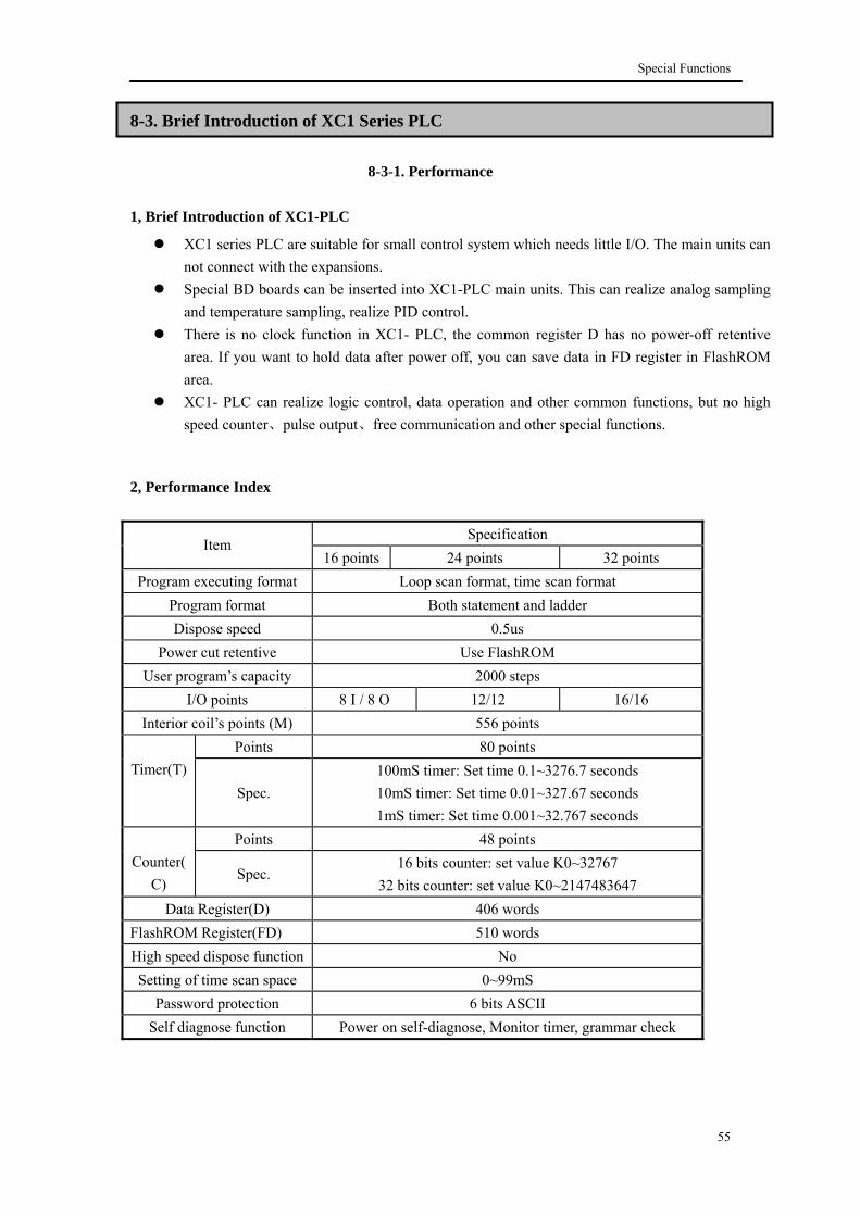
Special Functions
55
8-3. Brief Introduction of XC1 Series PLC
8-3-1. Performance 1, Brief Introduction of XC1-PLC 2, Performance Index
Specification Item
16 points 24 points 32 points Program executing format Loop scan format, time scan format
Program format Both statement and ladder Dispose speed 0.5us
Power cut retentive Use FlashROM User program’s capacity 2000 steps
I/O points 8 I / 8 O 12/12 16/16 Interior coil’s points (M) 556 points
Points 80 points Timer(T)
Spec. 100mS timer: Set time 0.1~3276.7 seconds 10mS timer: Set time 0.01~327.67 seconds 1mS timer: Set time 0.001~32.767 seconds
Points 48 points Counter(
C) Spec.
16 bits counter: set value K0~32767 32 bits counter: set value K0~2147483647
Data Register(D) 406 words FlashROM Register(FD) 510 words High speed dispose function No Setting of time scan space 0~99mS
Password protection 6 bits ASCII Self diagnose function Power on self-diagnose, Monitor timer, grammar check
XC1 series PLC are suitable for small control system which needs little I/O. The main units can not connect with the expansions.
Special BD boards can be inserted into XC1-PLC main units. This can realize analog sampling and temperature sampling, realize PID control.
There is no clock function in XC1- PLC, the common register D has no power-off retentive area. If you want to hold data after power off, you can save data in FD register in FlashROM area.
XC1- PLC can realize logic control, data operation and other common functions, but no high speed counter、pulse output、free communication and other special functions.

Special Functions
56
8-3-2. Statements XC1 series PLC includes all SFC statements of XC3 series PLC, part of applied statements, no special function statements. XC1 series PLC has the following applied instructions:
Sort Mnemonic Function CJ Condition jump
CALL Call subroutine SRET Subroutine return STL Flow start
STLE Flow end SET Open the assigned flow, close the current flow ST Open the assigned flow, not close the current flow
FOR Start of a FOR-NEXT loop NEXT End of a FOR-NEXT loop
Program Flow
FEND First end MOV Move
BMOV Block move FMOV Fill move FWRT FlashROM written MSET Zone set ZRST Zone reset
SWAP The high and low byte of the destinated devices are
exchanged
Data Move
XCH Exchange ADD Addition SUB Subtraction MUL Multiplication DIV Division INC Increment DEC Decrement
MEAN Mean WAND Word And WOR Word OR
WXOR Word exclusive OR CML Compliment
Data Operation
NEG Negative
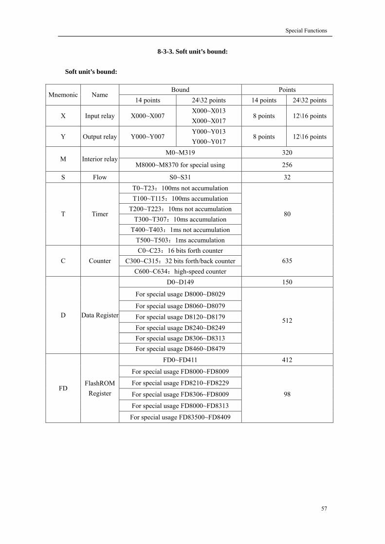
Special Functions
57
8-3-3. Soft unit’s bound:
Soft unit’s bound:
Bound Points Mnemonic Name
14 points 24\32 points 14 points 24\32 points
X Input relay X000~X007 X000~X013 X000~X017
8 points 12\16 points
Y Output relay Y000~Y007 Y000~Y013 Y000~Y017
8 points 12\16 points
M0~M319 320 M Interior relay
M8000~M8370 for special using 256
S Flow S0~S31 32 T0~T23:100ms not accumulation T100~T115:100ms accumulation
T200~T223:10ms not accumulation T300~T307:10ms accumulation
T400~T403:1ms not accumulation
T Timer
T500~T503:1ms accumulation
80
C0~C23:16 bits forth counter C300~C315:32 bits forth/back counter C Counter
C600~C634:high-speed counter 635
D0~D149 150
For special usage D8000~D8029
For special usage D8060~D8079 For special usage D8120~D8179 For special usage D8240~D8249 For special usage D8306~D8313
D Data Register
For special usage D8460~D8479
512
FD0~FD411 412
For special usage FD8000~FD8009
For special usage FD8210~FD8229
For special usage FD8306~FD8009
For special usage FD8000~FD8313
FD FlashROM
Register
For special usage FD83500~FD8409
98

Special Functions
58
8-4. XC5 series PLC
8-4-1. Performance 1, Brief introduction of XC5 series 2, Performance Index
Specification Item
32 points 48 points 60 points Program executing format Loop scan format, time scan format
Program format Both statement and ladder Dispose speed 0.5us
Power cut retentive Use FlashROM and Li battery User program’s capacity 2500 steps 10000 steps
I/O points 18 I / 14 O 28/20 36/24 Interior coil’s points (M) 8512 points
Points 620 points Timer(T)
Spec. 100mS timer: Set time 0.1~3276.7 seconds 10mS timer: Set time 0.01~327.67 seconds 1mS timer: Set time 0.001~32.767 seconds
Points 635 points Counter(
C) Spec.
16 bits counter: set value K0~32767 32 bits counter: set value K0~2147483647
Data Register(D) 8512 words FlashROM Register(FD) 2048 words High speed dispose function High speed counter, pulse output, external interrupt Setting of time scan space 0~99mS
Password protection 6 bits ASCII Self diagnose function Power on self-diagnose, Monitor timer, grammar check
XC5 series PLC covers all functions of XC1 series、XC3 series, also the interior source space is larger than XC1 and XC3 series; XC5 series PLC also have CANbus function, which can realize complex communication network function. For the detailed CANbus function, please refer to “TU6-8.CAN Bus (XC5 series) UT

Special Functions
59
8-4-2. Soft unit’s bound:
Soft unit’s bound:
Bound Points Mnemonic Name
32 points 48\60 points 32 points 48\60 points
X Input relay X000~X021 X000~X033 X000~X047
18 points 28\36 points
Y Output relay Y000~Y015 Y000~Y023 Y000~Y027
14 points 20\24 points
M0~M2999 【M3000~M7999】 8000 M Interior relay
M8000~M8511 for special using 512
S Flow S0~S511【S512~S1023】 1024 T0~T99:100ms not accumulation T100~T199:100ms accumulation
T200~T299:10ms not accumulation T300~T399:10ms accumulation
T400~T499:1ms not accumulation T500~T599:1ms accumulation
T Timer
T600~T618:1ms with interruption precise time
620
C0~C299:16 bits forth counter C300~C589:32 bits forth/back counter C Counter
C600~C634:high-speed counter 635
D0~D3999 【D4000~D7999】 8000 D Data Register
For special usage D8000~D8511 512
FD0~FD1535 4096 FD
FlashROM Register For special usage FD8000~FD8009 1024


