1©2022 Renesas Electronics Corporation January 11, 2022
DescriptionThe Renesas XL devices (XO and VCXO options) are ultra-precision crystal oscillators with 750 to 890fs typical phase jitter over 12kHz to 20MHz bandwidth. Available in a wide frequency range from 0.750MHz to 1350MHz, the XL series crystal oscillators utilize a family of proprietary ASICs, with a key focus on noise reduction technologies.
The 3rd order Delta Sigma Modulator reduces noise to the levels that are comparable to traditional Bulk Quartz and SAW oscillators. With short lead-time, low cost, low noise, wide frequency range, excellent ambient performance, the XL devices are an excellent choice over the conventional technologies. The XL (XO option) devices have stabilities as tight as ±20ppm and the XL (VCXO option) devices have ±50ppm APR. Either option provides extremely quick delivery for both standard and custom frequencies.
Pin Assignments
(XO Option)NOTE: To minimize power supply line noise, a 0.01μF bypass capacitor should be placed between VDD (Pin 6) and GND (Pin 3).
(VCXO Option)NOTE: To minimize power supply line noise, a 0.01μF bypass capacitor should be placed between VDD (Pin 6) and GND (Pin 3).
Features▪ Output types: LVDS, LVPECL, LVCMOS▪ Phase jitter (12kHz to 20MHz): 750fs to 890fs typical▪ Supply voltage: 2.5V or 3.3V▪ Package options:
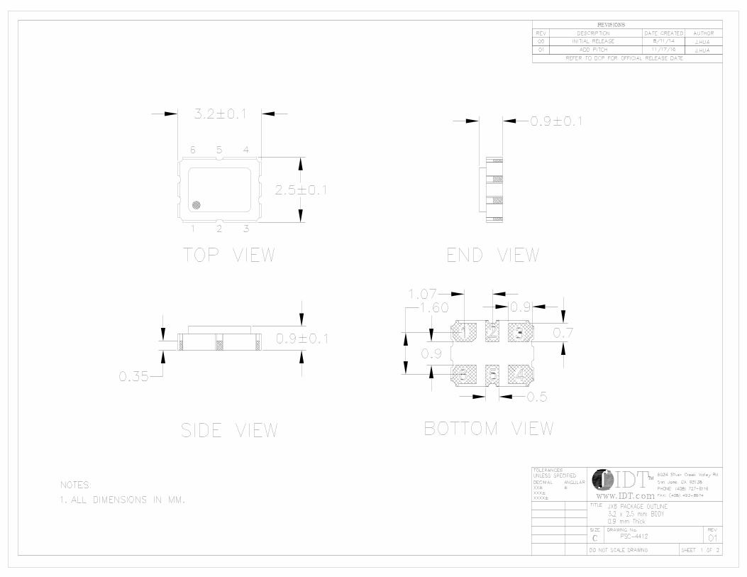
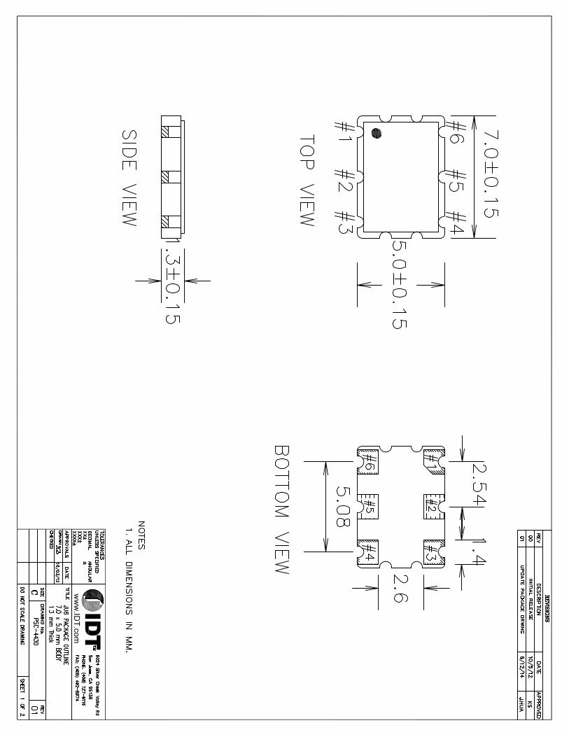
• 3.2 × 2.5 × 1.0 mm (not available for VCXO)• 5.0 × 3.2 × 1.2 mm• 7.0 × 5.0 × 1.3 mm
▪ Operating temperature: -20°C to +70°C• Frequency stability options: ±20, ±25, ±50, or ±100 ppm
(XO only)• ±50ppm APR (VCXO only)
▪ Operating temperature: -40°C to +85°C• Frequency stability options: ±25, ±50, or ±100 ppm
(XO only)• ±50ppm APR (VCXO only)
▪ Operating temperature: -40°C to +105°C (XO only)• Frequency stability options: ±50 or ±100 ppm
▪ kV of 85ppm/volt typical from 0.5VDC to VDD (VCXO only)• Better than ±10% linearity for Vc range
1 2 3
456
E/D
/ N
C
NC
/ E
/D
OU
T
OU
T2
VD
D
GN
D
1 2 3
456
Vc
E/D
OU
T
OU
T2
VD
D
GN
D
XLDatasheet
XL Family of Low Phase Noise Quartz-based PLL Oscillators
2©2022 Renesas Electronics Corporation January 11, 2022
XL Datasheet
Pin Descriptions Table 1. XO Pin Description
[a] Pulled high internally.[b] Low = output disabled.[c] Do not connect for LVCMOS. For XLVCMOS, both OUT and OUT2
are ON and in opposite phase.See Ordering Information (XO) for more details.
Table 2. VCXO Pin Description
[a] Pulled high internally.[b] Low = output disabled.See Ordering Information (VCXO) for more details.
Number Name Description
1 E/DNC
Enable/Disable [a][b]
No connect
2 NCE/D
No connectEnable/Disable [a][b]
3 GND Connect to ground
4 OUT Output
5 OUT2 Complementary output [c]
6 VDD Supply voltage
Number Name Description
1 Vc Voltage control
2 E/D Enable/Disable [a][b]
3 GND Connect to ground
4 OUT Output
5 OUT2 Complementary output (NC LVCMOS)
6 VDD Supply voltage
3©2022 Renesas Electronics Corporation January 11, 2022
XL Datasheet
Ordering Information (XO)
Table 3. Frequency Stability and Operating Temperature Decoder
“Precision” and “Temperature Range” Codes Operating TemperatureFrequency Stability
Minimum Maximum Units
“8” and “X” -20°C to +70°C -20 +20 ppm
“6” and “X” -20°C to +70°C -25 +25 ppm
“5” and “X” -20°C to +70°C -50 +50 ppm
“0” and “X” -20°C to +70°C -100 +100 ppm
“6” and “I” -40°C to +85°C -25 +25 ppm
“5” and “I” -40°C to +85°C -50 +50 ppm
“0” and “I” -40°C to +85°C -100 +100 ppm
“5” and “K” -40° to +105°C -50 +50 ppm
“0” and “K” -40° to +105°C -100 +100 ppm
XLFamily and ASIC
LOutput Type
5Package
3Voltage
5Precision
125.000000Frequency
ITemperature Range
I: Industrial range: ‐ 40 to +85 °C K: Extended industrial range : ‐40 to +105 °C X: Extended commercial range : ‐20 to +70 °C
125.000000 listed in MHz as example3 digits before decimal and 6 digits after decimal
000.750000 to 000.999999 75kHz to 999.999kHz001.000000 to 009.999999 1MHz to 9.999999MHz
010.000000 to 099.999999 10MHz to 99.999999MHz
100.000000 to 999.999999 100MHz to 999.999999MHz
A00.000000 to A99.999999 1000MHz to 1099.999MHz
B00.000000 to B99.999999 1100MHz to 1199.999MHz
C00.000000 to C99.999999 1200MHz to 1299.999MHz
D00.000000 to D50.000000 1300MHz to 1350MHz
0: ±100ppm 5: ±50ppm 6: ±25ppm 8: ±20ppm
2: 2.5 VDC ±5% 3: 3.3 VDC ±5%
3: 3.2 x 2.5 mm
5: 5.0 x 3.2 mm
7: 7.0 x 5.0 mm
H: LVCMOS Enable/Disable Pin 1
J: LVCMOS Enable/Disable Pin 2
L: LVDS Enable/Disable Pin 1 M: LVDS Enable/Disable Pin 2 P: LVPECL Enable/Disable Pin 1 Q: LVPECL Enable/Disable Pin 2 X: XLVCMOS Comp HCMOS Enable/Disable Pin 1*
Y: XLVCMOS Comp HCMOS Enable/Disable Pin 2*
XL: 1,000 fs jitter
See table below for more details.
* XLVCMOS: Complimentary HCMOS where both outputs are ON and in opposite phase.
See table below for more details.
4©2022 Renesas Electronics Corporation January 11, 2022
XL Datasheet
Ordering Information (VCXO)
XLFamily and ASIC
LOutput Type
5Package
3Voltage
V 125.000000Frequency
ITemperature Range
I: Industrial range: ‐ 40 to +85 °C X: Extended commercial range : ‐20 to +70 °C
125.000000 listed in MHz as example3 digits before decimal and 6 digits after decimal
000.750000 to 000.999999 75kHz to 999.999kHz001.000000 to 009.999999 1MHz to 9.999999MHz
010.000000 to 099.999999 10MHz to 99.999999MHz
100.000000 to 999.999999 100MHz to 999.999999MHz
A00.000000 to A99.999999 1000MHz to 1099.999MHz
B00.000000 to B99.999999 1100MHz to 1199.999MHz
C00.000000 to C99.999999 1200MHz to 1299.999MHz
D00.000000 to D50.000000 1300MHz to 1350MHz
V: VCXO option
2: 2.5 VDC ±5% 3: 3.3 VDC ±5%
5: 5.0 x 3.2 mm
7: 7.0 x 5.0 mm
H: LVCMOS Enable/Disable
L: LVDS Enable/Disable P: LVPECL Enable/Disable
XL: 1,000 fs jitter
5©2022 Renesas Electronics Corporation January 11, 2022
XL Datasheet
ContentsDescription . . . . . . . . . . . . . . . . . . . . . . . . . . . . . . . . . . . . . . . . . . . . . . . . . . . . . . . . . . . . . . . . . . . . . . . . . . . . . . . . . . . . . . . . . . . . . . . . . . . . . . 1Pin Assignments. . . . . . . . . . . . . . . . . . . . . . . . . . . . . . . . . . . . . . . . . . . . . . . . . . . . . . . . . . . . . . . . . . . . . . . . . . . . . . . . . . . . . . . . . . . . . . . . . . 1
(XO Option) . . . . . . . . . . . . . . . . . . . . . . . . . . . . . . . . . . . . . . . . . . . . . . . . . . . . . . . . . . . . . . . . . . . . . . . . . . . . . . . . . . . . . . . . . . . . . . . . . 1(VCXO Option) . . . . . . . . . . . . . . . . . . . . . . . . . . . . . . . . . . . . . . . . . . . . . . . . . . . . . . . . . . . . . . . . . . . . . . . . . . . . . . . . . . . . . . . . . . . . . . 1
Features . . . . . . . . . . . . . . . . . . . . . . . . . . . . . . . . . . . . . . . . . . . . . . . . . . . . . . . . . . . . . . . . . . . . . . . . . . . . . . . . . . . . . . . . . . . . . . . . . . . . . . . . 1Pin Descriptions . . . . . . . . . . . . . . . . . . . . . . . . . . . . . . . . . . . . . . . . . . . . . . . . . . . . . . . . . . . . . . . . . . . . . . . . . . . . . . . . . . . . . . . . . . . . . . . . . . 2Ordering Information (XO) . . . . . . . . . . . . . . . . . . . . . . . . . . . . . . . . . . . . . . . . . . . . . . . . . . . . . . . . . . . . . . . . . . . . . . . . . . . . . . . . . . . . . . . . . . 3Ordering Information (VCXO) . . . . . . . . . . . . . . . . . . . . . . . . . . . . . . . . . . . . . . . . . . . . . . . . . . . . . . . . . . . . . . . . . . . . . . . . . . . . . . . . . . . . . . . . 4Absolute Maximum Ratings . . . . . . . . . . . . . . . . . . . . . . . . . . . . . . . . . . . . . . . . . . . . . . . . . . . . . . . . . . . . . . . . . . . . . . . . . . . . . . . . . . . . . . . . . 6ESD Compliance . . . . . . . . . . . . . . . . . . . . . . . . . . . . . . . . . . . . . . . . . . . . . . . . . . . . . . . . . . . . . . . . . . . . . . . . . . . . . . . . . . . . . . . . . . . . . . . . . 6Mechanical Testing . . . . . . . . . . . . . . . . . . . . . . . . . . . . . . . . . . . . . . . . . . . . . . . . . . . . . . . . . . . . . . . . . . . . . . . . . . . . . . . . . . . . . . . . . . . . . . . 6Solder Reflow Profile . . . . . . . . . . . . . . . . . . . . . . . . . . . . . . . . . . . . . . . . . . . . . . . . . . . . . . . . . . . . . . . . . . . . . . . . . . . . . . . . . . . . . . . . . . . . . . 6DC Electrical Characteristics . . . . . . . . . . . . . . . . . . . . . . . . . . . . . . . . . . . . . . . . . . . . . . . . . . . . . . . . . . . . . . . . . . . . . . . . . . . . . . . . . . . . . . . . 7AC Electrical Characteristics . . . . . . . . . . . . . . . . . . . . . . . . . . . . . . . . . . . . . . . . . . . . . . . . . . . . . . . . . . . . . . . . . . . . . . . . . . . . . . . . . . . . . . . 10Output Waveforms – LVDS . . . . . . . . . . . . . . . . . . . . . . . . . . . . . . . . . . . . . . . . . . . . . . . . . . . . . . . . . . . . . . . . . . . . . . . . . . . . . . . . . . . . . . . . 13Output Waveforms – LVPECL . . . . . . . . . . . . . . . . . . . . . . . . . . . . . . . . . . . . . . . . . . . . . . . . . . . . . . . . . . . . . . . . . . . . . . . . . . . . . . . . . . . . . . 13Output Waveforms – LVCMOS . . . . . . . . . . . . . . . . . . . . . . . . . . . . . . . . . . . . . . . . . . . . . . . . . . . . . . . . . . . . . . . . . . . . . . . . . . . . . . . . . . . . . 14Package Outline Drawings . . . . . . . . . . . . . . . . . . . . . . . . . . . . . . . . . . . . . . . . . . . . . . . . . . . . . . . . . . . . . . . . . . . . . . . . . . . . . . . . . . . . . . . . . 15Marking Diagrams . . . . . . . . . . . . . . . . . . . . . . . . . . . . . . . . . . . . . . . . . . . . . . . . . . . . . . . . . . . . . . . . . . . . . . . . . . . . . . . . . . . . . . . . . . . . . . . 15Revision History . . . . . . . . . . . . . . . . . . . . . . . . . . . . . . . . . . . . . . . . . . . . . . . . . . . . . . . . . . . . . . . . . . . . . . . . . . . . . . . . . . . . . . . . . . . . . . . . . 16
6©2022 Renesas Electronics Corporation January 11, 2022
XL Datasheet
Absolute Maximum RatingsStresses above the ratings listed below can cause permanent damage to the device. These ratings, which are standard values for Renesas commercially rated parts, are stress ratings only. Functional operation of the device at these or any other conditions above those indicated in the operational sections of the specifications is not implied. Exposure to absolute maximum rating conditions for extended periods can affect product reliability. Electrical parameters are guaranteed only over the recommended operating temperature range.
ESD Compliance
Mechanical Testing
Solder Reflow Profile
Table 4. Absolute Maximum Ratings
Item RatingVDD -0.5 to +5.0V E/D -0.5V to VDD + 0.5VOUT -0.5V to VDD + 0.5VStorage Temperature -55°C to 125°CMaximum Junction Temperature 125°CCore Current 65mA maximumTheta JA JU6
7.0 × 5.0 × 1.3 mm75.9 °C/W JS6
5.0 × 3.2 × 1.2 mm89.6 °C/W JX6
3.2 × 2.5 × 1.0 mm94.7 °C/W
Theta JB 48.6°C/W 54.3 °C/W 66.8 °C/W
Table 5. ESD Compliance
Human Body Model (HBM 1000V
Machine Model (MM) 150V
Table 6. Mechanical Testing
Parameter Test MethodMechanical Shock Drop from 75cm to hardwood surface–3 times.Mechanical Vibration 10–55Hz, 1.5mm amplitude, 1 minute sweep; 2 hours each in 3 directions (X, Y, Z).High Temperature Burn-in Under power at 125°C for 2000 hours.Hermetic Seal He pressure: 4 ±1kgf/cm2 2 hour soak.
tP 10 seconds Max within 5°C of 260°C peak
Ramp down not to exceed 6°C/s
Ramp up 3°C/s Max
120 ±20 seconds in pre-heating
area
50 ±10 seconds
above 225°C reflow area
400 seconds MAX from +25°C to 260°C peak
25°C
160°C
180°C
225°C
260°C
7©2022 Renesas Electronics Corporation January 11, 2022
XL Datasheet
DC Electrical CharacteristicsTable 7. 3.3V IDD DC Electrical Characteristics
VDD = 3.3V ±5%, TA = -20°C to +70°C; -40°C to +85°C, -40°C to +105°C.
Symbol Parameter Output Type Conditions Minimum Typical Maximum Units
IDD Power Supply Current
LVDS
0.75MHz to 40MHz. — 32 37
mA
40+MHz to 220MHz. — 40 47
220+MHz to 630MHz. — 49 57
630+MHz to 1350MHz. — 72 100
LVPECL[a]
[a] Without termination resistors.
0.75MHz to 40MHz. — 26 31
40+MHz to 220MHz. — 38 45
220+MHz to 630MHz. — 56 64
630+MHz to 1350MHz. — 96 120
LVCMOS
0.75MHz to 20MHz. — 27 32
20+MHz to 50MHz. — 32 35
50+MHz to 130MHz. — 43 47
130+MHz to 200MHz. — 48 55
200+MHz to 250MHz. — 48 60
Table 8. 2.5V IDD DC Electrical Characteristics
VDD = 2.5V ±5%, TA = -20°C to +70°C; -40°C to +85°C, -40°C to +105°C.
Symbol Parameter Output Type Conditions Minimum Typical Maximum Units
IDD Power Supply Current
LVDS
0.75MHz to 20MHz. — 24 26
mA
20+MHz to 220MHz. — 29 34
220+MHz to 630MHz. — 36 44
630+MHz to 1000MHz. — 46 65
LVPECL[a]
[a] Without termination resistors.
0.75MHz to 20MHz. — 20 33
20+MHz to 220MHz. — 28 41
220+MHz to 630MHz. — 41 63
630+MHz to 1000MHz. — 56 72
LVCMOS
0.75MHz to 20MHz. — 17 22
20+MHz to 50MHz. — 23 25
50+MHz to 100MHz. — 28 29
100+MHz to 130MHz. — 30 32
130+MHz to 160MHz. — 32 35
160+MHz to 180MHz. — 33 37
8©2022 Renesas Electronics Corporation January 11, 2022
XL Datasheet
Table 9. LVDS DC Electrical Characteristics
VDD = 3.3V, 2.5V ±5%, TA = -20°C to +70°C; -40°C to +85°C, -40°C to +105°C. Below are guaranteed for listed standard frequencies.
Symbol Parameter Conditions Minimum Typical Maximum Units
VOD Differential Output VoltageVDD = 3.3V ±5%. — — 0.6
V
VDD = 2.5V ±5%. — — 0.4
VOS Output Offset VoltageVDD = 3.3V ±5%. — — 1.3
VDD = 2.5V ±5%. — — 1.25
VIHEnable/Disable Input High Voltage (Output enabled)
— 70% VDD — —
VILEnable/Disable Input Low Voltage(Output disabled)
— — — 30% VDD
Table 10. LVPECL DC Electrical Characteristics
VDD = 3.3V, 2.5V ±5%, TA = -20°C to +70°C; -40°C to +85°C, -40°C to +105°C. Below are guaranteed for listed standard frequencies.
Symbol Parameter Conditions Minimum Typical Maximum Units
VOD Differential Output VoltageVDD = 3.3V ±5%. 2.055 2.405
V
VDD = 2.5V ±5%. — 1.4 —
VOS Output Offset VoltageVDD = 3.3V ±5%. 1.305 1.65
VDD = 2.5V ±5%. — 0.68 —
VIHEnable/Disable Input High Voltage (Output enabled)
— 70% VDD — —
VILEnable/Disable Input Low Voltage(Output disabled)
— — — 30% VDD
9©2022 Renesas Electronics Corporation January 11, 2022
XL Datasheet
Table 11. LVCMOS DC Electrical Characteristics
VDD = 3.3V, 2.5V ±5%, TA = -20°C to +70°C; -40°C to +85°C, -40°C to +105°C. Below are guaranteed for listed standard frequencies.
Symbol Parameter Conditions Minimum Typical Maximum Units
VOH Output High Voltage
VDD = 3.3V ±5%.0.75MHz to 150MHz. 90% VDD — —
V
150+MHz to 250MHz. 80% VDD — —
VDD = 2.5V ±5%.0.75MHz to 160MHz. 90% VDD — —
160+MHz to 180MHz. 80% VDD — —
VOL Output Low Voltage
VDD = 3.3V ±5%.0.75MHz to 150MHz. — — 10% VDD
150+MHz to 250MHz. — — 20% VDD
VDD = 2.5V ±5%.0.75MHz to 160MHz. — — 10% VDD
160+MHz to 180MHz. — — 20% VDD
VIHEnable/Disable Input High Voltage(Output enabled)
— — 70% VDD — —
VILEnable/Disable Input Low Voltage(Output disabled)
— — — — 30% VDD
10©2022 Renesas Electronics Corporation January 11, 2022
XL Datasheet
AC Electrical CharacteristicsTable 12. 3.3V AC Electrical Characteristics
VDD = 3.3V ±5%, TA = -20°C to +70°C; -40°C to +85°C, -40°C to +105°C.
Symbol Parameter Test Condition Minimum Typical Maximum Units
F Output Frequency Range
LVDS. 0.75 — 1350
MHzLVPECL. 0.75 — 1350
LVCMOS. 0.75 — 250
Frequency Stability
Temperature = -20°C to +70°C.
-20-25-50
-100
—
+20+25+50
+100
ppm
Temperature = -40°C to +85°C.-25-50
-100—
+25+50
+100ppm
Temperature = -40°C to +105°C. -50-100 — +50
+100 ppm
Output Load
LVDS. Differential. — 100 —Ω
LVPECL. VDD - 2.0V. — 50 —
LVCMOS. To GND. — 15 — pF
TST Start-up Time Output valid time after VDD meets minimum specified level. — — 10 ms
tR Output Rise Time
LVDS.20% to 80% Vpp.
— — 400ps
LVPECL. — — 400
LVCMOS. 10% to 90% VDD. — — 3 ns
tF Output Fall Time
LVDS.80% to 20% Vpp.
— — 400ps
LVPECL. — — 400
LVCMOS. 90% to 10% VDD. — — 3 ns
ODC Output Clock Duty Cycle
LVDS. 45 — 55
%LVPECL. 45 — 55
LVCMOS.FOUT < 62.5MHz. 45 — 55
FOUT > 62.5MHz. 40 — 60
TOE Output Enable/ Disable Time — — — 100 ns
JPER Period Jitter, RMS
LVDS. — 3 —
psLVPECL. — 5.8 —
LVCMOS. FOUT = 125MHz. — 5 —
RJ Random Jitter
LVDS. — 1.3 —
psLVPECL. — 1.29 —
LVCMOS. FOUT = 125MHz. — 0.6 —
11©2022 Renesas Electronics Corporation January 11, 2022
XL Datasheet
DJ Deterministic Jitter
LVDS. — 5.8 —
psLVPECL. — 9.3 —
LVCMOS. FOUT = 125MHz. — 10 —
TJ Total Jitter
LVDS. — 23.6 —
psLVPECL. — 27.7 —
LVCMOS. FOUT = 125MHz. — 19 —
fJITTER Phase Jitter (12kHz–20MHz)
LVDS. — 890 —
fsLVPECL. — 860 —
LVCMOS. FOUT = 125MHz. — 750 —
Table 13. 2.5V AC Electrical Characteristics
VDD = 2.5V ±5%, TA = -20°C to +70°C; -40°C to +85°C, -40°C to +105°C.
Symbol Parameter Test Condition Minimum Typical Maximum Units
F Output Frequency Range
LVDS. 0.75 — 1000
MHzLVPECL. 0.75 — 1000
LVCMOS. 0.75 — 180
Frequency Stability
Temperature = -20°C to +70°C.
-20-25-50
-100
—
+20+25+50
+100
ppm
Temperature = -40°C to +85°C.-25-50
-100—
+25+50
+100ppm
Temperature = -40°C to +105°C. -50-100 — +50
+100 ppm
Output Load
LVDS. Differential. — 100 —Ω
LVPECL. VDD - 2.0V. — 50 —
LVCMOS. To GND. — 15 — pF
TST Start-up Time Output valid time after VDD meets minimum specified level. — — 10 ms
tR Output Rise Time
LVDS.20% to 80% Vpp.
— — 400ps
LVPECL. — — 400
LVCMOS. 10% to 90% VDD. — — 3.5 ns
tF Output Fall Time
LVDS.80% to 20% Vpp.
— — 400ps
LVPECL. — — 400
LVCMOS. 90% to 10% VDD. — — 3 ns
Table 12. 3.3V AC Electrical Characteristics (Cont.)
VDD = 3.3V ±5%, TA = -20°C to +70°C; -40°C to +85°C, -40°C to +105°C.
Symbol Parameter Test Condition Minimum Typical Maximum Units
12©2022 Renesas Electronics Corporation January 11, 2022
XL Datasheet
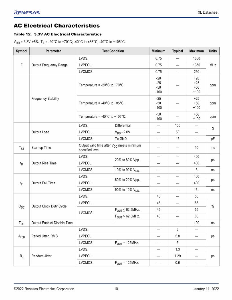
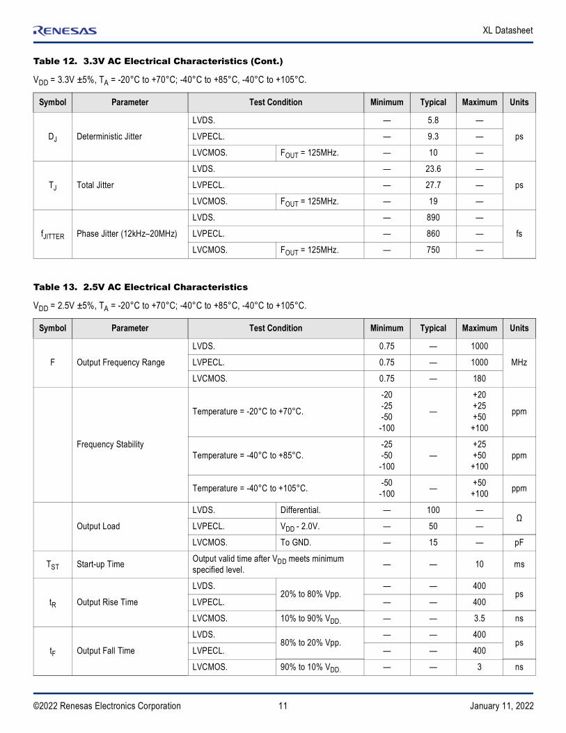
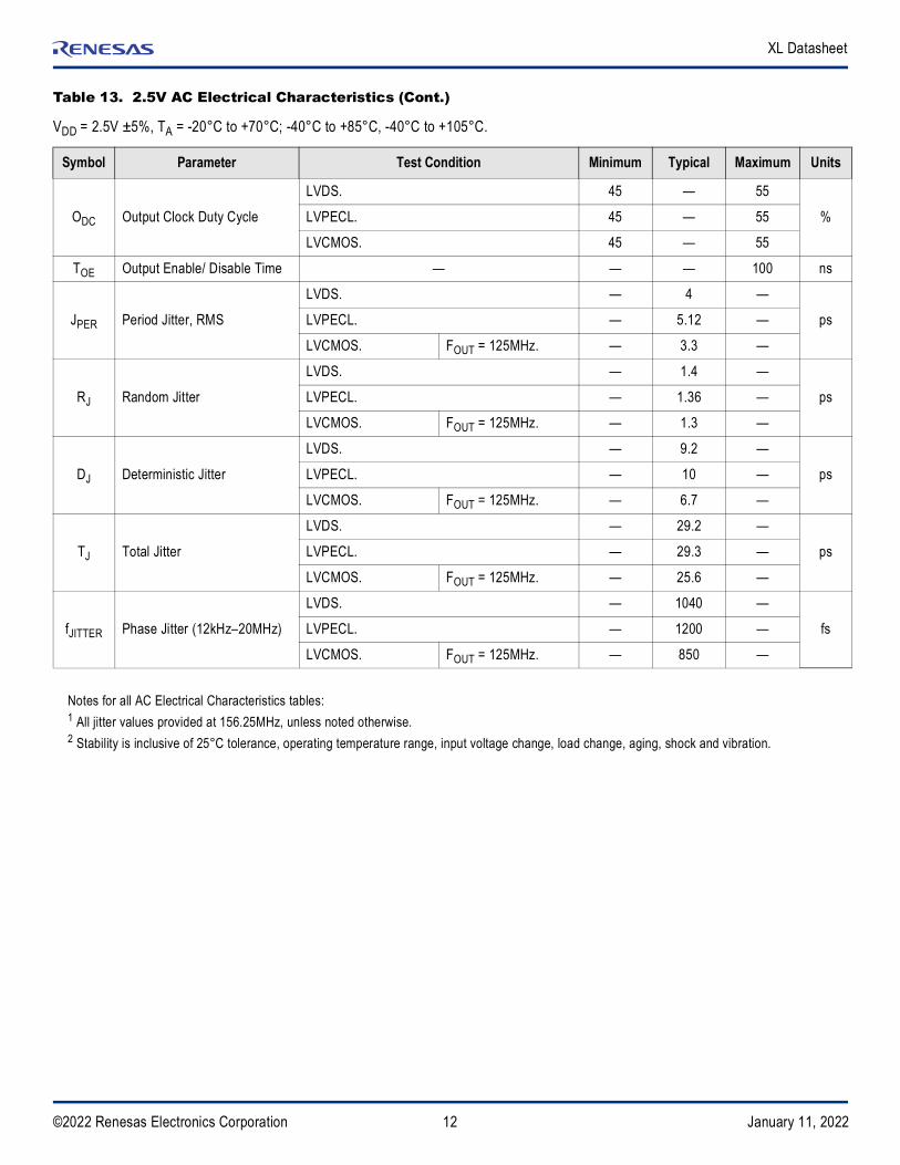
Notes for all AC Electrical Characteristics tables:1 All jitter values provided at 156.25MHz, unless noted otherwise.2 Stability is inclusive of 25°C tolerance, operating temperature range, input voltage change, load change, aging, shock and vibration.
ODC Output Clock Duty Cycle
LVDS. 45 — 55
%LVPECL. 45 — 55
LVCMOS. 45 — 55
TOE Output Enable/ Disable Time — — — 100 ns
JPER Period Jitter, RMS
LVDS. — 4 —
psLVPECL. — 5.12 —
LVCMOS. FOUT = 125MHz. — 3.3 —
RJ Random Jitter
LVDS. — 1.4 —
psLVPECL. — 1.36 —
LVCMOS. FOUT = 125MHz. — 1.3 —
DJ Deterministic Jitter
LVDS. — 9.2 —
psLVPECL. — 10 —
LVCMOS. FOUT = 125MHz. — 6.7 —
TJ Total Jitter
LVDS. — 29.2 —
psLVPECL. — 29.3 —
LVCMOS. FOUT = 125MHz. — 25.6 —
fJITTER Phase Jitter (12kHz–20MHz)
LVDS. — 1040 —
fsLVPECL. — 1200 —
LVCMOS. FOUT = 125MHz. — 850 —
Table 13. 2.5V AC Electrical Characteristics (Cont.)
VDD = 2.5V ±5%, TA = -20°C to +70°C; -40°C to +85°C, -40°C to +105°C.
Symbol Parameter Test Condition Minimum Typical Maximum Units
13©2022 Renesas Electronics Corporation January 11, 2022
XL Datasheet
Output Waveforms – LVDS
Output Waveforms – LVPECL
Oscillator Symmetry
Output Levels/Rise Time/Fall Time Measurements
OUTPUT 2
OUTPUT 1
OUTPUT 2
OUTPUT 1
50% VPP
VOH
VOL
VOD
½ Period
Period
TR TF
20% to 80% VPP
Ideally, Symmetry should be 50/50 for ½ period –Other expressions are 45/55 or 55/45
50% VPP VOS
Oscillator Symmetry
Rise Time/Fall Time Measurements
OUTPUT 2
OUTPUT 1
OUTPUT 2
OUTPUT 1
50% VPP
VOH
VOL
VOH
VOL
½ Period
Period
TR TF
20% to 80% VPP
15©2022 Renesas Electronics Corporation January 11, 2022
XL Datasheet
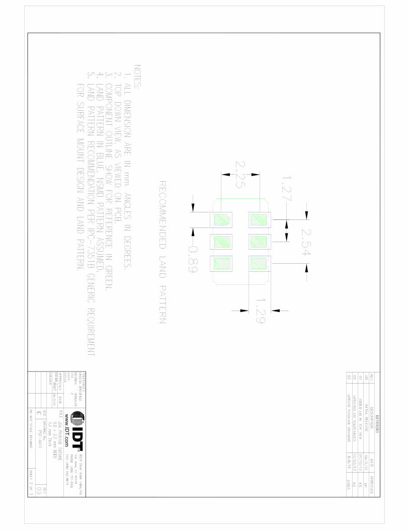
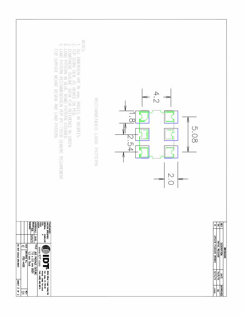
Package Outline DrawingsThe package outline drawings (JS6, JX6, JU6) are appended at the end of this document. The package information is the most current data available.
Marking DiagramsJX6 3.2 × 2.5 mm Package Option (example based on XLH320010.000000I)
JS6 5.0 × 3.2 mm Package Option (example based on XLH536210.380000I)
JU6 7.0 × 5.0 mm Package Option (example based on XLH735004.915200X)
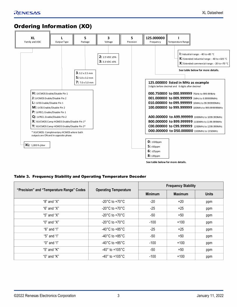
▪ Line 1: • “010” denotes last three digits to the left of the decimal point as shown in the above
example. This number will vary depending upon the frequency value selected in the orderable part number.
• “YW” denotes the last digit of the year and work week the part was assembled.
▪ Line 1: • “XL” = family; “H” = output type; “5” = package size; “3” = voltage; “6” = precision
level. This number will vary depending upon the output type, voltage, and precision values selected in the orderable part number.
▪ Line 2:• “210” denotes last three digits to the left of the decimal point as shown in the above
example. This number will vary depending upon the frequency value selected in the orderable part number.
• “YW” denotes the last digit of the year and work week the part was assembled.
▪ Line 1: • “XL” = family; “H” = output type; “7” = package size; “3” = voltage; “5” = precision
level. This number will vary depending upon the output type, voltage, and precision values selected in the orderable part number.
▪ Line 2:• “004” denotes last three digits to the left of the decimal point as shown in the above
example. This number will vary depending upon the frequency value selected in the orderable part number.
• “YW” denotes the last digit of the year and work week the part was assembled.
16©2022 Renesas Electronics Corporation January 11, 2022
XL Datasheet
Revision History
Revision Date Description of Change
January 11, 2022 ▪ Removed Aging parameters in Table 12 and Table 13.▪ Added footnote 2 after Table 13.
December 1, 2021 Updated Frequency Stability values in Table 12 and Table 13.
November 23, 2021 Added Frequency Stability and Operating Temperature Decoder table after Ordering Information.
August 18, 2021 Moved XO and VCXO ordering information tables to be just after Pin Descriptions.
January 19, 2021 ▪ Removed 4-pin package description table, figure, and package drawing references.▪ Added footnote for pin 5 in Table 1.▪ Added footnote under “Output Type” in XO Ordering Information.
January 12, 2021 Added Marking Diagrams section and updated Package Outline Drawings links.
October 27, 2020 Added pin counts to Output Type in XO ordering table.
September 21, 2020 Added typical IDD to tables. Added more frequency ranges to IDD tables. Updated H to be LVCMOS in order code.
April 27, 2020 Updated ODC parameter. 2nd LVCMOS row to be changed from <= to > 62.5 MHz.
September 7, 2018 Updated frequency stability options value from ±20ppm to ±25ppm for -40°C to +85°C XO only.
June 25, 2018 ▪ Updated Package Outline Drawings section.
May 4, 2018 ▪ Added XO and VCXO options.▪ Updated description and Features sections.▪ Updated Package Outline Drawings section.▪ Added VCXO Ordering Information decoder diagram.
January 12, 2018 Initial release.
Corporate HeadquartersTOYOSU FORESIA, 3-2-24 Toyosu,Koto-ku, Tokyo 135-0061, Japanwww.renesas.com
Contact InformationFor further information on a product, technology, the most up-to-date version of a document, or your nearest sales office, please visit:www.renesas.com/contact/
TrademarksRenesas and the Renesas logo are trademarks of Renesas Electronics Corporation. All trademarks and registered trademarks are the property of their respective owners.
IMPORTANT NOTICE AND DISCLAIMER
RENESAS ELECTRONICS CORPORATION AND ITS SUBSIDIARIES (“RENESAS”) PROVIDES TECHNICAL SPECIFICATIONS AND RELIABILITY DATA (INCLUDING DATASHEETS), DESIGN RESOURCES (INCLUDING REFERENCE DESIGNS), APPLICATION OR OTHER DESIGN ADVICE, WEB TOOLS, SAFETY INFORMATION, AND OTHER RESOURCES “AS IS” AND WITH ALL FAULTS, AND DISCLAIMS ALL WARRANTIES, EXPRESS OR IMPLIED, INCLUDING, WITHOUT LIMITATION, ANY IMPLIED WARRANTIES OF MERCHANTABILITY, FITNESS FOR A PARTICULAR PURPOSE, OR NON-INFRINGEMENT OF THIRD PARTY INTELLECTUAL PROPERTY RIGHTS.
These resources are intended for developers skilled in the art designing with Renesas products. You are solely responsible for (1) selecting the appropriate products for your application, (2) designing, validating, and testing your application, and (3) ensuring your application meets applicable standards, and any other safety, security, or other requirements. These resources are subject to change without notice. Renesas grants you permission to use these resources only for development of an application that uses Renesas products. Other reproduction or use of these resources is strictly prohibited. No license is granted to any other Renesas intellectual property or to any third party intellectual property. Renesas disclaims responsibility for, and you will fully indemnify Renesas and its representatives against, any claims, damages, costs, losses, or liabilities arising out of your use of these resources. Renesas' products are provided only subject to Renesas' Terms and Conditions of Sale or other applicable terms agreed to in writing. No use of any Renesas resources expands or otherwise alters any applicable warranties or warranty disclaimers for these products.
(Rev.1.0 Mar 2020)
© 2020 Renesas Electronics Corporation. All rights reserved.