ZnO morphological, structural and optical properties control by electrodeposition potential sweep rate Elena Matei, Monica Enculescu, Nicoleta Preda, Ionut Enculescu * National Institute of Materials Physics, Atomistilor St. 105 bis, 77125 Magurele, Ilfov, Romania article info Article history: Received 7 April 2011 Received in revised form 16 January 2012 Accepted 25 March 2012 Keywords: Oxides Semiconductors Electrochemical techniques abstract ZnO films were electrodeposited from an aqueous nitrate bath on ITO/glass substrates. The process was performed not by the usual potentiostatic approach but by using potential ramps with different sweep rates. We tested these ramps in both directions i.e. either towards electronegative (direct) or electro- positive (inverse) potential. As expected, the samples prepared in different deposition conditions show different morphology, different quality of crystalline structure and different optical properties. By employing inverse ramps we prepared films with high quality structural and optical properties. We assume that in these conditions the growth is followed by an etching process which preferentially removes the areas with high defect concentration and leads to the formation of hollow hexagonal prisms. Ó 2012 Elsevier B.V. All rights reserved. 1. Introduction Zinc oxide is a semiconductor with several features which make it a candidate for the development of a new generation of electronic or optoelectronic products. Its applications range from catalysts to sensors and transparent electrodes for solar cells [1e5]. Typically ZnO is a highly transparent n type semiconductor with a direct band gap of about 3.3 eV and has an exciton binding energy of 60 meV. This makes it extremely interesting for light emitting applications in UV range such as light emission diodes and lasers. Besides these specific physical properties, there are some charac- teristics which make ZnO even more attractive for potential applications, highly important being its natural abundance and low toxicity. One characteristic of ZnO, which tends to become more important lately, is related to its nanostructures polymorphism. Up to this moment, a wide range of nanoparticles were obtained by means of a variety of methods: tetrapods, columns, nanobrushes and nanocombs, flowers, petals, platelets, wires, rods and tubules [6e9]. The morphology of the product is a direct consequence of the preparation path and, in the case of ZnO, we deal with an astonishing variety ranging from simplest chemical precipitation methods to highly complex molecular beam epitaxial processes [10e13]. Not only is the morphology a direct consequence of the preparation method but also the structure and the defect concentration are important parameters which can be finely tuned by choosing the appropriate preparation parameters. Electrochemical deposition represents a convenient way to prepare nanostructured films or arrays of nanostructures of zinc oxide on conducting substrates. Major advantages of the method are its low cost and scalability. Numerous reports were presented in literature regarding the electrodeposition of zinc oxide from both aqueous [14e18] and nonaqueous baths [19]. In most cases the aqueous deposition was performed using either zinc chloride or zinc nitrate on a variety of seeded or seedless substrates. The deposition process leads to polycrystalline films, typical morphol- ogies being columns or platelets. Electrochemical bath additives are used for better control of deposits’ properties [20]. The electrode- position process is carried in either potentiostatic or galvanostatic mode. Deposition at non-constant currents (dynamic polarization currents) was also performed proving that by such method one can better tune morphological and structural properties of the deposit, complex morphology structures being obtained [21]. Another aspect of interest is related to the fabrication of hollow structures e extremely important when thinking that in this way the specific surface of the nanostructures is increased [22,23]. In the present paper we report our results regarding the control of properties of zinc oxide films by electrodeposition using linear varying voltage (voltage ramps). The deposition was performed using an aqueous nitrate bath without any additives. We used different voltage sweeping rates with both positive and negative sign. The samples obtained were characterized in terms of morphology, structure and optical properties. We found that by * Corresponding author. Tel.: þ40 723012084; fax: þ40 21 369 01 77. E-mail address: encu@infim.ro (I. Enculescu). Contents lists available at SciVerse ScienceDirect Materials Chemistry and Physics journal homepage: www.elsevier.com/locate/matchemphys 0254-0584/$ e see front matter Ó 2012 Elsevier B.V. All rights reserved. doi:10.1016/j.matchemphys.2012.03.101 Materials Chemistry and Physics 134 (2012) 988e993
Transcript
at SciVerse ScienceDirect
Materials Chemistry and Physics 134 (2012) 988e993
0254-0584/$ e see front matter � 2012 Elsevier B.V.doi:10.1016/j.matchemphys.2012.03.101
a b s t r a c t
ZnO films were electrodeposited from an aqueous nitrate bath on ITO/glass substrates. The process wasperformed not by the usual potentiostatic approach but by using potential ramps with different sweeprates. We tested these ramps in both directions i.e. either towards electronegative (direct) or electro-positive (inverse) potential. As expected, the samples prepared in different deposition conditions showdifferent morphology, different quality of crystalline structure and different optical properties. Byemploying inverse ramps we prepared films with high quality structural and optical properties. Weassume that in these conditions the growth is followed by an etching process which preferentiallyremoves the areas with high defect concentration and leads to the formation of hollow hexagonal prisms.
� 2012 Elsevier B.V. All rights reserved.
1. Introduction
Zinc oxide is a semiconductor with several features which makeit a candidate for the development of a newgeneration of electronicor optoelectronic products. Its applications range from catalysts tosensors and transparent electrodes for solar cells [1e5]. TypicallyZnO is a highly transparent n type semiconductor with a directband gap of about 3.3 eV and has an exciton binding energy of60 meV. This makes it extremely interesting for light emittingapplications in UV range such as light emission diodes and lasers.Besides these specific physical properties, there are some charac-teristics which make ZnO even more attractive for potentialapplications, highly important being its natural abundance and lowtoxicity. One characteristic of ZnO, which tends to become moreimportant lately, is related to its nanostructures polymorphism. Upto this moment, a wide range of nanoparticles were obtained bymeans of a variety of methods: tetrapods, columns, nanobrushesand nanocombs, flowers, petals, platelets, wires, rods and tubules[6e9]. The morphology of the product is a direct consequence ofthe preparation path and, in the case of ZnO, we deal with anastonishing variety ranging from simplest chemical precipitationmethods to highly complex molecular beam epitaxial processes[10e13]. Not only is the morphology a direct consequence of thepreparation method but also the structure and the defect
þ40 21 369 01 77.
All rights reserved.
concentration are important parameters which can be finely tunedby choosing the appropriate preparation parameters.
Electrochemical deposition represents a convenient way toprepare nanostructured films or arrays of nanostructures of zincoxide on conducting substrates. Major advantages of the methodare its low cost and scalability. Numerous reports were presented inliterature regarding the electrodeposition of zinc oxide from bothaqueous [14e18] and nonaqueous baths [19]. In most cases theaqueous deposition was performed using either zinc chloride orzinc nitrate on a variety of seeded or seedless substrates. Thedeposition process leads to polycrystalline films, typical morphol-ogies being columns or platelets. Electrochemical bath additives areused for better control of deposits’ properties [20]. The electrode-position process is carried in either potentiostatic or galvanostaticmode. Deposition at non-constant currents (dynamic polarizationcurrents) was also performed proving that by such method one canbetter tune morphological and structural properties of the deposit,complex morphology structures being obtained [21]. Anotheraspect of interest is related to the fabrication of hollow structureseextremely important when thinking that in this way the specificsurface of the nanostructures is increased [22,23].
In the present paper we report our results regarding the controlof properties of zinc oxide films by electrodeposition using linearvarying voltage (voltage ramps). The deposition was performedusing an aqueous nitrate bath without any additives. We useddifferent voltage sweeping rates with both positive and negativesign. The samples obtained were characterized in terms ofmorphology, structure and optical properties. We found that by
E. Matei et al. / Materials Chemistry and Physics 134 (2012) 988e993 989
using linear varying voltages we were able to control not only themorphology of the deposit but also its structural quality andluminescence properties.
2. Experimental
A simple, 0.05 M Zn(NO3)2 aqueous solution without any addi-tives was used as electrolyte. The substrates were lab made ITOcovered glass (2.5�1 cm2) prepared by DC sputtering and witha measured resistance of 30 ohm/sample. The electrodepositionwas performed in a thermostated double walled glass electro-chemical cell at a temperature of 90 �C controlled by a recirculatingthermostat. During the deposition process no agitation was used.
We used a typical three electrode set-up with a saturatedcalomel (SCE) reference and a 2 cm2 platinum plate counter elec-trode. The reference electrode was connected to the electro-chemical cell by a 20 cm long salt bridge filled with KCl, in order toavoid its contamination and to maintain its temperature close toroom. The deposition process was controlled by a PAR 2273potentiostat galvanostat.
X-ray diffractionwas performed using a Bruker AXS D8 Advanceinstrument with Cu Ka radiation (l¼ 0.154 nm). Morphology wascharacterized using a Zeiss EVO 50 scanning electron microscope(SEM) with LaB6 cathode. Optical reflection spectroscopy wasemployed for determining the band gap value of the material. Weused a Perkin Elmer Lambda 45 spectrophotometer with an inte-grating sphere for measuring the reflected light. The sample wasmounted with its normal at an angle of 8 degrees relative to theincident beam, in this manner both specular and diffuse reflectedlight being collected and therefore total reflection being taken intoaccount. Optical luminescence was measured using an EdinburghInstruments LS 900 spectrometer with a Xe excitation lamp of450 W, double monochromators on both excitation and emissionarms, and photon counting detection.
3. Results and discussion
Themain purpose of our work was to find a simple path in orderto prepare nanostructured ZnO films with low defect content andhighly controlled morphology.
The cathode reactions taking place during the ZnO electrode-position processes are the following:
2e�þNO3�þH2O/NO2
�þ 2OH� (1)
Zn2þþ 2OH�/ Zn(OH)2/ ZnOYþH2O (2)
or the global reaction:
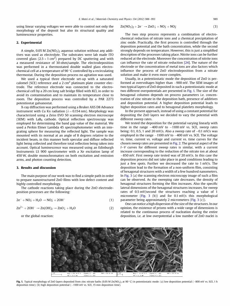
Fig. 1. Typical morphology of ZnO layers deposited from zinc nitrate baths (0.05 M Zn(NO3
deposition time); (b) high deposition potential (�1100 mV vs. SCE, 15 min deposition time)
Zn(NO3)2þ 2e�/ ZnOYþNO3�þNO2
� (3)
The two step process represents a combination of electro-chemical reduction of nitrate ions and a chemical precipitation ofzinc oxide. Practically, the first process is controlled through thedeposition potential and the bath concentration, while the secondstrongly depends on temperature. However, this is just a simplifieddescription of the processes taking place. Nitrite ions can be furtherreduced at the electrode. Moreover the concentration of nitrite ionscan influence the rate of nitrate reduction [24]. The nature of theelectrode or the concentration of metal ions are also factors whichinfluence the process of ZnO electrodeposition from a nitratesolution and make it even more complex.
Usually, in a potentiostatic mode the deposition of ZnO is per-formed at overvoltages higher than �900 mV. The SEM images oftwo typical layers of ZnO deposited in such a potentiostatic mode attwo different overpotentials are presented in Fig. 1. The size of thehexagonal columns depends on process parameters i.e. concen-tration of zinc nitrate in the deposition bath, presence of additivesand deposition potential. A higher deposition potential leads tohigher deposition rates and to hexagonal platelets morphology.
In the present approach, instead of using a constant potential fordepositing the ZnO layers we decided to vary the potential withdifferent sweep rates.
We tested the deposition for the potential varying linearly withtime in the range �400 mV to �1100 mV vs. SCE, sweep ratesbeing: 0.1, 0.5, 1 and 20 mV/s. Also a sweep rate of �0.1 mV/s wasemployed in the range �1100 mV to �400 mV vs. SCE. The voltagevs. time, current vs. voltage and current vs. time curves for thechosen sweep rates are presented in Fig. 2. The general aspect of theIeV curves for different sweep rates is similar, with a currentincrease corresponding to the reduction of the nitrate ion at about�850 mV. First sweep rate tested was of 20 mV/s. In this case thedeposition process did not take place in good conditions leading tojust a few spots. Further we decreased the rate to 1 mV/s. Thedeposition lead to the formation of a non-uniform film, consistingof hexagonal structures with awidth of a few hundred nanometers.In Fig. 3 (a) the scanning electron microscopy image of such a filmcan be observed. As the sweeping rate decreases, the density ofhexagonal structures forming the film increases. Also the specificlateral dimensions of the hexagonal structures increases, for sweeprates of 0.5 mV/second the structures reaching a value of 1micrometer (Fig. 3 (b)) and for 0.1 mV/s this morphologicalparameter being approximately 2 micrometers (Fig. 3 (c)).
Onecannotice ahighdispersionof the sizeof the structures. In ouropinion, the existence of prisms with a wide range of dimensions isrelated to the continuous process of nucleation during the entiredeposition, i.e. at low overpotential a low number of ZnO nuclei is
)2 at 90 �C) in potentiostatic mode: (a) low deposition potential (�800 mV vs. SCE, 1 h.
Fig. 2. (a) Potential versus time, (b) current vs. potential and (c) current vs. time measured for different sweep rates.
E. Matei et al. / Materials Chemistry and Physics 134 (2012) 988e993990
formed. As the voltage increases, these nuclei grow but also othernuclei are formed. Finally we end up with a layer of zinc oxidehexagonal columns with the size depending on the nucleationmoment. When lower sweep rates are used the size of the biggeststructures increases, thesehaving the longest time to grow.Onedetail
Fig. 3. ZnO layer deposited with a sweep rate o
which has to be emphasized is the high uniformity of the depositedlayer (awider area of a deposited film can be observed in Fig. 3 (d)), inprinciple up-scaling of the deposition cell being straightforward.
Being clear that the density of nuclei is related to the depositionpotential and that when using a direct polarization sweep one will
f (a) 1 mV/s, (b) 0.5 mV/s, (c), (d) 0.1 mV/s.
Fig. 5. X-ray diffraction data for samples deposited at (a) 1 mV/s; (b) 0.5 mV/s; (c)0.1 mV/s; (d) �0.1 mV/s.
E. Matei et al. / Materials Chemistry and Physics 134 (2012) 988e993 991
deal with scattered dimensions we decided to test the reversedprocess, i.e. starting at the higher (more electronegative) over-potential, i.e. at �1100 mV and decreasing the potential down to�400 mV. In Fig. 4 (a) one can observe the film obtained in theseconditions, with a sweep rate of �0.1 mV/s. It is obvious that thesize dispersion of the hexagonal columns is much lower incomparison to the case when direct polarization was performed.Somehow puzzling is the fact that some of the structures appearhollow.
We repeated the process for 2 and 4 sweeps and it looks like thecenter of the hexagonal structures was completely removed, thefinal result being an array of uniform, well oriented hexagonalhollow structures (Fig. 4 (c) and (d)). As in the case of the filmsprepared by direct polarization, the deposition leads to layers ofhexagonal structures uniform over large areas.
The next step in our investigation was to determine the struc-tural properties of the investigated ZnO films. In Fig. 5, the X-raydifractograms for the set of samples deposited with different sweeprates is presented. Hexagonal zinc oxide lines are visible. The firstobservationwhich can bemade based on the diffraction data is thatin the case of the sample with the highest sweeping rate the signalto noise ratio is relatively low, the difraction signal being muchstronger for the samples prepared at lower sweeping rates. Thus,signal to noise ratio is most probably related to films thickness andshould be, and is higher for the thicker film (the film deposited forlonger time i.e. at lower sweep rates). As expected from the scan-ning electron microscopy images, a preferential orientation of theZnO prisms e evidenced by the intensity of the (002) peak in theplot of diffraction data e can be observed for all the samples.Further, the (002) peak is the most intense one for each sample butthe texture degree depends on the sweep rate of the potential (onecan observe the variation of the ratio between the intensity of thepeaks corresponding to planes (002) and (100) for example for thefirst three plots corresponding to 1 mV/s; 0.5 mV/s and 0.1 mV/srespectively).
Fig. 4. ZnO layers deposited using reversed potential sweep of �
In terms of texture, it is interesting to compare the diffracto-grams of the samples deposited at a rate of 0.1 mV/s in direct andreversed polarization of the sweep rate. A comparison in this casemakes even more sense since the total deposition time andtherefore the thickness should be the same for the two cases. Boththe diffraction signal intensity and the sample texture are higher forthe reverse potential sweep deposition, for similar deposition time,this indicating an enhanced quality of the crystalline structure anda better orientation of the prism shaped crystalites forming thefilm.
Scanning electron microscopy images of films cross sectionssupport this affirmation. Thus in Fig. 6 a set of cross section imagesfor samples deposited at different sweep rates are presented. Onecan observe for the samples where direct sweep was performed
0.1 mV/s: (a) one sweep, (b) 2 sweeps, (c) and (d) 4 sweeps.
Fig. 6. Cross sectionof ZnO layers deposited with a sweep rate of (a) 1 mV/s, (b) 0.5 mV/s, (c) 0.1 mV/s, (d) 0.1 mV/s in reversed sweeping mode.
Fig. 7. Reflection spectra of a set of samples prepared with different sweep rates.
E. Matei et al. / Materials Chemistry and Physics 134 (2012) 988e993992
a clear relation between the thickness of the film and the time spanof the process. For the case of the sample deposited in a reversesweep mode, two aspects must be noted. First, the thickness of thefilm is much smaller than in the case of the sample deposited witha direct sweep mode, a ratio of approximately 1e4. Second, thedirection of the prisms is much closer to perpendicular on thesubstrate in comparison to the case of the samples deposited bydirect sweeping direction. The differences in the thickness of thefilmmay be easily explained by the dissolution process which takesplace at electropositive enough potentials for the sample depositedin a reverse mode. However, nucleation must play a key role in thebetter orientation along the c axis of the samples deposited byreverse sweeping.
Since ZnO is a material with high potential for optoelectronicapplications its optical and electrical properties are extremelyimportant. Optical reflection measurements were performed inorder to determine the band gap value of the material. The resultsare presented in Fig. 7. The strong decrease in reflection corre-sponding to the band to band transition is strongly visible. For thesamples which were grown with high sweep rates a strongabsorption close to the band to band transition can be observed, it’sorigin being unknown at the moment. Using the Kubelka Munkrepresentation of the reflection data we calculated the band gapvalue. This value is 3.25 eV� 0.05 eV, a value which corresponds todata previously reported.
Photoluminescence represents a property of zinc oxide of greatimportance for applications. There are several characteristic emis-sion bands of the material: the excitonic emission related to thenear e band to band transition with the peak at approximately380 nm and the deffect bands with a wide maxima at wavelengthsin the range 500e600 nm [25e28]. In our case we expect anemission maxima at 570e580 nm related to oxygen intersititals.This emission peak is characteristic to ZnO prepared by wetmethods, where excess oxygen is present, as opposed to the520 nm peak related to oxygen vacancies and observed for samplesprepared in low oxygen environment.
Usually the exciton peak is highly sensitive to material quality,a high defect content leading to low ultraviolet emission of zincoxide. An important reason fueling the research of new improvedzinc oxide preparation methods is the desire to fabricate ultravioletlight emitting devices based on it.
In our case it is easy to observe the strong connection betweenthe X-ray data and the luminescence (Fig. 8). Thus, for the sampleswith low structural quality, i.e. high defect content, the excitonicpeak is not visible. For the sample grownwith direct and low sweeprate, the exitonic peak becomes visible and comparable with thedefect emission band. For the sample with reverse polarization theexcitonic emission is strong while the defect related emission isbarely visible. This beahaviour is a consequence of the defectcontent of the samples. Apparentlywhen the deposition takes place
Fig. 8. Photoluminescence emission spectra for samples grown using (a) 1 mV/s, (b)0.5 mV/s, (c) 0.1 mV/s and (d) �0.1 mV/s sweep rates.
E. Matei et al. / Materials Chemistry and Physics 134 (2012) 988e993 993
by reversed polarization, in the initial step the nucleation processtakes place. Further, the deposition of zinc oxide takes place forpotentials more electronegative than the reduction potential ofnitrate ions.When the potential becomesmore electropositive thanthis reduction potential, predominant becomes a process of disso-lution. Low structural quality and high defect concentration areasare the first to dissolute. Thus, the process which takes place in thismanner has, as a result of this combination of deposition anddissolution processes, the highest morphological uniformity asproved by SEM images, the highest structural quality and presentexcellent optical properties.
A natural comparison of the process can bemadewith the resultsreported for pulsed electrodeposition of zinc oxide [e.g. 29e31].However, there are striking differences between the final results ofthe two types of processes. Thus, pulsed electrodeposition, ina classic way, i.e. pulse length of several seconds or lower thana second and several thousand repetitions, leads to results compa-rable to those obtained using constant potential processes, differ-ences being induced by changing ratios between diffusion andreaction time. As an example in Ref. [30] pulsed electrodepositionlead to films with smoother surface and therefore improved opticaltransmittance. In the present case we deal with a process for whichthe time constant is of the order of thousands off seconds and therepetition of the process is of maximum three, this being mostprobably the reason for the differences. However for a betterunderstanding of the process and in order to increase the controlover the phenomena taking place at the electrode one can think ofa multistep deposition process with constant potential steps andwhich may lead to similar results to the one described above. Mostprobably at least three steps need to be defined in terms of potentialand time, corresponding to nucleation, growth and etching.
4. Conclusions
By using electrodeposition from a simple nitrate bath withlinearly varying potential at different sweep rates and sense weprepared zinc oxide films. We found that the sweep rates and sensestrongly influence the properties of the material: morphologicalstructural and optical. Using direct sweeping, hexagonal columnswith high dimensional dispersion are obtained. As the sweepingrate decreases the structural quality of the films increases, for thelowest measured sweeping rate the ultraviolet emission is alsoobserved proving a low defect content of the sample.
Extremely interesting is the sweeping in opposite directionnamely from electronegative towards more positive potential. Inthis case the result is a film with high structural quality, its intenseultraviolet emission proving also a low defect concentration. Themorphology of the film is different in this case, the structures beinghexagonal hollow prisms. The dispersion of dimensions is muchlower in this case. It is most probable that the process steps arebetter defined: a nucleation process takes place at electronegativepotential followed by the growth process and by a selectivedissolution. Several reverse sweeping process lead to highlyuniform. Hollow ZnO structures with high UV emission. Such singlestep deposition of high quality ZnO films using a cheap, scalabletechnique may be extremely important for fabricating a wide rangeof optoelectronic devices.
Acknowledgments
The authors acknowledge the financial support of the NucleuProgramme of the Romanian Ministry of Education and Researchand of the contract Eurocores Nanoiobip financed by UEFISCDI.
References
[1] M.H. Huang, S. Mao, H. Feick, H. Yan, Y. Wu, H. Kind, E. Weber, R. Russo,P. Yang, Science 292 (2001) 1897e1899.
[2] N. Kumar, A. Dorfman, Jong-in Hahm, Nanotechnology 17 (2006) 2875.[3] M. Law, L.E. Greene, J.C. Johnson, R. Saykally, P. Yang, Nature Materials 4
(2005) 455e459.[4] L.J. Bie, X.N. Yana, J. Yina, Y.Q. Duana, Z.H. Yuan, Sensors and Actuators B 126
(2007) 604e608.[5] M. Taher Maghsoodloua, A. Hassankhania, H. Reza Shateriana, S. Mostafa
Habibi-Khorasania, E. Mosaddegh, Tetrahedron Letters 48 (2007) 1729e1734.[6] Z.L. Wang, Materials Today 7 (2004) 26e33.[7] Y. Yan, L. Zhou, J. Zou, Y. Zhang, Applied Physics A 94 (2009) 559e565.[8] D. Banerjee, J. Rybczynski, J.Y. Huang, D.Z. Wang, K. Kempa, Z.F. Ren, Applied
Physics A 80 (2005) 749e752.[9] J. Wu, S. Chen, S. Gao, Materials Chemistry and Physics 122 (2010) 301e304.
[10] J.H. Zheng, Q. Jiang, J.S. Lian, Applied Surface Science 257 (2011) 5083e5087.[11] Z. Li, Z. Hu, F. Liu, J. Sun, H. Huang, X. Zhang, Y. Wang, Materials Letters 65
(2011) 809e811.[12] K. Haga, T. Suzuki, Y. Kashiwaba, H. Watanabe, B.P. Zhang, Y. Segawa, Thin
Solid Films 433 (2003) 131e134.[13] W.I. Parka, S.-J. Ana, Gyu-Chul Yia, Hyun M. Jang, Journal of Materials Research
16 (2001) 1358e1362.[14] S. Peulon, D. Lincot, Advanced Materials 8 (1996) 166e170.[15] S. Peulon, D. Lincot, Journal of the Electrochemical Society 145 (1998)
864e874.[16] M. Izaki, T. Omi, Journal of the Electrochemical Society 144 (1997)
1949e1952.[17] T. Yoshida, D. Komatsu, N. Shimokawa, H. Minoura, Thin Solid Films 451e452
(2004) 166e169.[18] B. Postels, A. Bakin, H.-H. Wehmann, M. Suleiman, T. Weimann, P. Hinze,
A. Waag, Applied Physics A 91 (2008) 595e599.[19] D. Gal, G. Hodes, D. Lincot, H.-W. Schock, Thin Solid Films 361e362 (2000)
79e83.[20] I. Enculescu, E. Matei, Mariana Sima, M. Enculescu, M. Sima, C. Ghica, Surface
and Interface Analysis 40 (2008) 556e560.[21] E. Rayon, J. Cembrero, B. Mari, Materials Letters 64 (2010) 2601e2604.[22] X. Ren, C.H. Jiang, D.D. Li, L. He, Materials Letters 62 (2008) 3114e3116.[23] J. Elias, C. Levy-Clement, M. Bechelany, J. Michler, G.-Y. Wang, Z. Wang,
L. Philippe, Advanced Materials 22 (2010) 1607e1612.[24] C. Milhano, D. Pletcher, in: R. White (Ed.), Modern Aspects of Electrochem-
istry, 45, 2009, pp. 1e55.[25] K. Vanheusden, W.L. Warren, C.H. Seager, D.R. Tallant, J.A. Voigt, B.E. Gnade,
Journal of Applied Physics 79 (1996) 7983e7990.[26] B.J. Jin, S. Im, S.Y. Lee, Thin Solid Films 366 (2000) 107e110.[27] A. van Dijken, E.A. Meulenkamp, D. Vanmaekelbergh, A. Meijerink, Journal of
Luminescence 87e89 (2000) 454e456.[28] Sheng-Nan Sun, B. Marí, Hong-Lin Wu, M. Mollar, Hai-Ning Cui, Applied
Surface Science 257 (2010) 985e989.[29] M.D. Reyes Tolosa, J. Orozco-Messana, L.C. Damonte, M.A. Hernandez-Fenol-
losa, Journal of The Electrochemical Society 158 (2011) D452eD455.[30] K. Nomura, N. Shibata, M. Maeda, Journal of The Electrochemical Society 149
(2002) F76eF80.[31] J. Lee, Y. Tak, Electrochemical and Solid-State Letters 4 (2001) C63eC65.