66
Seed Money Fund MATERIALS SCIENCE AND ENGINEERING
| Date post: | 21-Feb-2023 |
| Category: |
Documents |
| Upload: | independent |
| View: | 0 times |
| Download: | 0 times |

Seed Money Fund
MATERIALS SCIENCE AND ENGINEERING
Materials Science and Engineering: Seed Money 59
Final Report Project Number: 3210-2031
A New Microwave-Driven Pack Cementation Coating ProcessJ. Kiggans,1 T. Tiegs,1 M. Losego,2 S. Nunn,1 L. Riester,1 M. Williams,1 and R. Lowden1
1Metals and Ceramics Division2Office of Science, Energy Research Undergraduate Laboratory Fellowship
Experiments were performed to determine if microwave heating can be used to apply diffusioncoatings to metal alloy parts. In order to maintain a broad scope for this project, three metal alloyswere selected which represent materials of interest for future research areas. These alloys included atool steel (A2), a low-carbon steel (1018), and a nickel-chrome super alloy (625). Three types ofdiffusion coating processes were chosen: aluminization, chromization, and boronization. Controlsamples were processed by conventional heating. Aluminum-, chrome-, and boron-based diffusioncoatings were successfully created using microwave heating. These microwave coatings show somesimilarities to the conventionally produced coatings, although significant differences also existed insome cases. Very encouraging results were obtained with the A2 tool steel.
IntroductionThe use of microwave (MW) energy or processing as
a tool for materials processing emerged during the late1950s, but only within the past two decades has MWresearch really gained a foothold in the scientificcommunity. Researchers in both the scientific andindustrial communities have begun to explore MWtechnology as a way to improve even well-establishedprocessing practices.1
Pack cementation is a surface modification techniqueprimarily used for metallic components to increaseoxidation/corrosion resistance, wear resistance, and/orsurface hardness. Pack cementation is a diffusion-basedtechnique in which the desired species diffuses into thematerial through the surface. This diffusion creates a solidsolution region near the surface with enhanced properties.Common diffusion-driven surface treatments includealuminizing, chromizing, and borodizing. The actual packcementation process involves packing the untreated metalparts in a powder bed or pack and then heat-treating attemperatures between 800–1000°C. The powder packconsists of three general components: the desired diffusionsource material, a halide activator (such as NaCl orNH4Cl), and an inert filler (typically alumina). At elevatedtemperatures, the source material reacts with the halide toform a gas, which permeates the porous pack. Uponreaching the surface of the sample, another reaction occurs,depositing the source material on the substrate. Due tothe high processing temperatures, the deposited elementtypically diffuses into the surface, leading to the desiredsurface treatment. The filler material is present simply todeter sintering.2 Due to its simplicity and ability to coateven complicated parts, pack cementation continues to bea popular surface treatment method.
Current knowledge surrounding MW processingpractices seems to indicate that pack cementation couldbe improved with the use of MW heating. Exposure of thepack cementation materials to MW energy should exploitthe unique characteristics of MW heating behavior, ascompared to conventional heating, which should provideseveral benefits. Depending on the dielectric propertiesof each component, they will absorb energy differentlyand therefore heat at different rates. It is well known thatdispersed metal particulates heat extremely well in a MWfurnace and they should do so in the pack cementationbed. In the above example, the aluminum powder wouldheat preferentially. The halide activator may or may notheat well by microwaves, depending on its dielectricproperties.3 For instance, the NH4Cl in the above examplewould heat better than the NaCl (based on dielectric losstangents), but neither would heat up as well as thealuminum. However, if one uses CuCl2 as the activator, itheats just as well as the aluminum. Thus, by choosingappropriate halides, that heat or do not heat, further controlof the cementation process can be obtained. In general,the inert filler powder would not heat well in a microwavefurnace if an oxide, such as Al2O3, were employed.However, if fillers such as SiC are used, it could also bemodified to tailor the heating response of the cementationpack.
Typically MW energy is confined within the furnacewithout much energy loss until there is an interaction withan absorber or the targeted sample (coupling). Hence, theenergy transfer has much greater efficiency than mostconventional heating methods, which employ radiantheating. Ordinarily, a dense metal part would not beexpected to heat with microwaves. Thus, MW exposure
60 FY 2003 ORNL Laboratory Directed Research and Development Annual Report
of the pack cementation process would most probablypreferentially heat the bed containing the precursor sourcematerial and the halide activator. However, even in themetal parts there is some microwave absorption in the wearsurface region. An estimate of the MW penetration (orskin depth) into a metal part during pack cementation canbe made using the following equation:
)FrequencyC(sistivityRe5030DepthSkin •=
As shown, the skin depth is dependent on theresistivity of the part and the MW frequency (C is aconstant and is normally equal to 1). Thus, the approximatepenetration depth at 2.45 GHz and a resistivity of 1 × 10-
4 W⋅cm is on the order of 10 µm. Because the resistivity ofmost metals increases with temperature, the penetrationdepth should also increase as the temperature increases.
Microwave heating offers several advantages overconventional heating, mainly because it can selectivelyheat materials in a multicomponent system, creating aunique temperature profile. The potential advantageswould include the following.1. Because the temperature gradients will be higher than
those in a conventional heating situation, theconcentration gradient of the diffusing species intothe component will also be steeper.4 In most cases,this should increase the enhancement of surfaceproperties and decrease the effects on bulk propertiesof the part being treated.
2. The process will be faster. Selective absorption ofthe MW energy will heat the packed bed rapidly totemperatures sufficient for the halide activator tooperate. Conversely, because the surroundinginsulation is cooler, the part should also cool faster.In addition, MW enhancement of diffusionalprocesses in the near-surface regions, if any, wouldfurther improve the kinetics during the treatment.5,6
3. The bulk properties of the treated part will undergoonly minimal alteration by thermal exposure. Sincethe process is faster, the parts are not subjected to thesame high temperatures for extended periods of timeas compared to the conventional heating situation.Consequently, less grain growth and othermicrostructural changes will occur that would affectthe bulk properties.7
4. Microwave pack cementation should be safer andmore environmentally friendly. With the heatingconfined to the volume directly surrounding the partto be treated, there should be less halide volatilityand therefore less chance for halides being releasedfrom the reaction crucible. Also, because of the
concentrated heat, it is possible that less halideactivator will be required for the process. In addition,since the metal MW cavity is relatively cold, it actsas a getter for fumes, which may evolve during thereaction. Thus, noxious by-products will not beexhausted from the furnace.
5. Because the MW process is faster, safer, and less aptto change bulk properties, it will also be more efficientand economical on a total life cycle basis.
Some challenges do remain, though, including dealingwith materials that poorly absorb MW power andcontrolling thermal runaway in samples that couple toowell. Although the metal substrates used for packcementation are expected to be MW reflectors,8 the metalpowders used as the source material are known to beexcellent couplers of MW radiation.8 Therefore, suchheating problems are not expected for this project.However, due to possible shielding effects of the metalsamples, it is difficult to predict the compositional andthermal uniformity. Furthermore, accurate measurementof temperatures in MW experiments has proven difficulthistorically due to temperature gradients that occurnaturally in such processes.9
Technical ApproachFor these experiments, we prepared cylindrical (1.25-
cm diam × 1.25 long) and rectangular (1.25 cm × 1.25 cm× 1.25 cm). Three types of diffusion coating processeswere chosen: aluminization, chromization, andboronization. For all three processs, the pack consisted ofNH4Cl as the activator and –325 mesh tabular aluminumoxide (Al2O3) as the filler. The depositing source materials(15 wt %) were aluminum metal powder (Al) foraluminization; chrome oxide (Cr2O3) for chromization; andboron carbide (B4C) powder for boronization. Afterplacing samples in the packing powder in an aluminacrucible, the crucible was sealed with a ceramic paste andan alumina lid, heated to 100°C to set the glue, andevacuated and backfilled twice with argon. Loadedcrucibles were heated at either 850 or 925°C for 4 h inflowing argon in either a 2.45-GHz MW furnace or in aconventional tube furnace. Control experiments wereperformed in which samples were heated in the aluminapowder without the NH4Cl activator and without the sourcepowder. Processed and control samples were weighed andmeasured both before and after surface treatment. Controland processed samples were analyzed using opticalmicroscopy, scanning electron microscopy, and energydispersive X-ray spectroscopy (EDS). The hardness valuesof control and boronized samples were measured usingboth a nano-indentor and a micro-hardness testing device.
Materials Science and Engineering: Seed Money 61
Results and AccomplishmentsAluminization Results
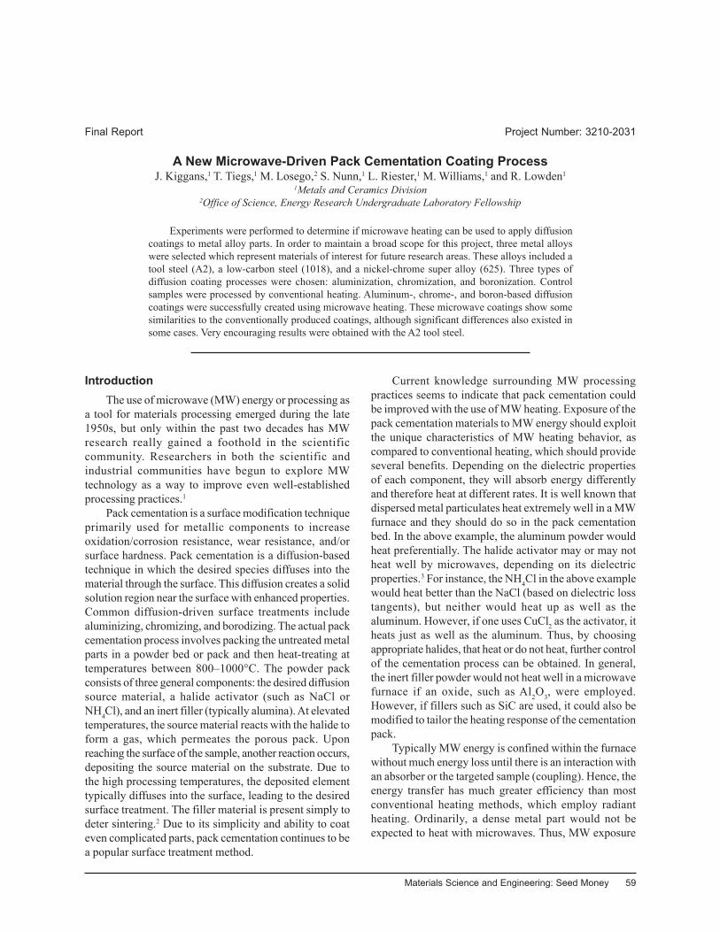
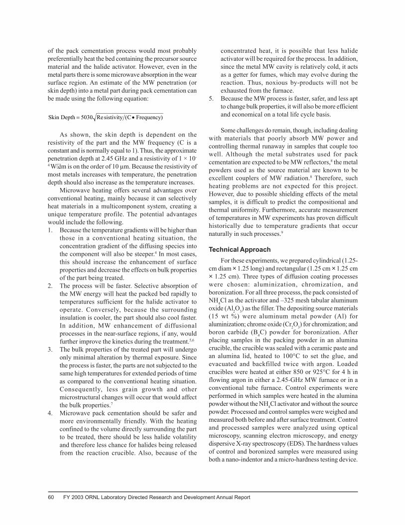
Aluminum-based coatings were successfullydeposited on all three alloys using MW heating.Approximately 800 W of power was needed to maintainthe temperature at 850 and 925°C for the 40 g of samplesand the ~425 g of packing powder. Coatings were alsodeposited on all alloys using conventional heating. Figure 1shows weight gain values obtained for the three metalalloys aluminized at 850 and 925°C using either MW orconventional heating. The results show that there was morealuminum deposited on the MW-treated samples at bothtemperatures. Scanning electron microscopic (SEM)examination of the samples was used to determine theextent of the aluminum diffusion into the samples. SEMexamination (photos not shown) show that the aluminumcoatings exist as both deposited and diffusion layers.Figures 2 and 3 show data generated from the SEMexamination of both the A2 tool steel and the 1018 steelprocessed by either microwave or conventional heating at850 or 925°C. The aluminized coatings were much thickerfor the A2 and 1018 steel alloys processed to 925°C byMW heating. The data also shows that most of this coating
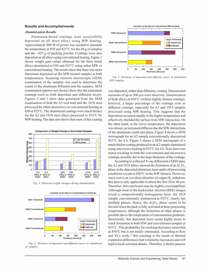
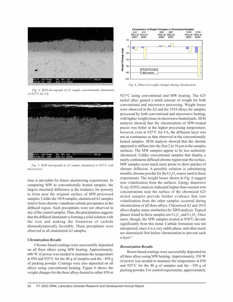
was deposited, rather than diffusion, coating. Dimensionalincreases of up to 300 µm were observed. Aluminizationof both alloys at 850°C yielded slightly thinner coatings;however, a larger percentage of the coatings exist asdiffusion coatings, especially for A2 and 1018 samplesprocessed using MW heating. This suggests that thedeposition occurred rapidly at the higher temperature andeffectively shielded the surface from MW interaction. Onthe other hand, at the lower temperature, the depositionwas slower, so increased diffusion due the MW interactionsof the aluminum could take place. Figure 4 shows a SEMmicrograph for an A2 sample conventionally aluminized925°C for 4 h. Figure 5 shows a SEM micrograph of amuch thicker coating produced in an A2 sample aluminizedusing microwave heating at 925°C for 4 h. Note there wasminor cracking in both the conventional and microwavecoatings, possibly due to the large thickness of the coatings.
According to collected X-ray diffraction (XRD) data,the A2 and 1018 alloys showed the formation of an Al5Fe2phase in the deposited aluminum layer under all processingconditions except at 850°C in the MW furnace. However,since iron is an excellent absorber of copper Ka radiation,this data is only applicable to about the first 20 to 40 µm.Therefore, this conclusion may be slightly oversimplified.Although most of the backscatter electron (BSE) imagesreveal a compositionally homogenous layer, the 1018sample conventionally aluminized at 925°C clearly hasmultiple phases. Hence, the Al5Fe2 phase seems to befavored when the pack is fully activated at these processingtemperatures, although the formation of other phases ispossible due to the temperature of concentration gradients.Structurally, this deposited layer seems highly prone tocrack formation in both MW and conventional samples at925°C. This probability for cracking decreases somewhatat 850°C but is not totally eliminated. According to Kooand Yu’s work,10 this cracking is the result of thermalexpansion differences (not volumetric increases) and willlead to local corrosion attacks. Therefore, a shorter process
Fig. 1. Observed weight changes during aluminization.
Fig. 2. Thickness of deposited and diffusion layers in aluminizedA2 samples.
Fig. 3. Thickness of deposited and diffusion layers in aluminized1018 samples.
62 FY 2003 ORNL Laboratory Directed Research and Development Annual Report
time is advisable for future aluminizing experiments. Incomparing MW to conventionally heated samples, thelargest structural difference is the tendency for porosityto form near the original surface of MW-processedsamples. Unlike the 1018 samples, aluminized A2 samplestend to form chrome-vanadium carbide precipitates in thediffused region. Such precipitates were not observed inany of the control samples. Thus, this precipitation suggeststhat the diffused aluminum is forming a solid solution withthe iron and making the formation of carbidethermodynamically favorable. These precipitates wereobserved in all aluminized A2 samples.
Chromization ResultsChrome-based coatings were successfully deposited
on all three alloys using MW heating. Approximately,600 W of power was needed to maintain the temperatureat 850 and 925°C for the 40 g of samples and the ~450 gof packing powder. Coatings were also deposited on allalloys using conventional heating. Figure 6 shows theweight changes for the three alloys heated to either 850 or
925°C using conventional and MW heating. The 625nickel alloy gained a small amount of weight for bothconventional and microwave processing. Weight losseswere observed in the A2 and the 1018 alloys for samplesprocessed by both conventional and microwave heating,with higher weight losses in microwave-heated parts. SEManalysis showed that the chromization of MW-treatedpieces was better at the higher processing temperature;however, even at 925°C for 4 h, the diffusion layer wasnot as continuous as that observed in the conventionallyheated samples. SEM analysis showed that the chromeappeared to diffuse into the first 2 to 10 µm at the samplessurfaces. The MW samples appear to be less uniformlychromized. Unlike conventional samples that display anearly continuous diffused chrome region near the surface,MW samples seem much more prone to show patches ofchrome diffusion. A possible solution is substitutingmetallic chrome powder for the Cr2O3 source used in theseexperiments. The weight losses shown in Fig. 6 suggestiron volatilization from the surfaces. Energy dispersiveX-ray (EDX) analysis indicated higher-than-normal ironconcentrations near the surface of the chromized 625nickel samples provide further evidence that ironvolatilization from the other samples occurred duringchromization of all three alloys. Chromized A2 and 1018alloys display many similarities by XRD analysis. Typicalphases found in these samples are Cr7C3 and Cr2O3. Oncemore, though, the MW samples treated at 850°C deviatesignificantly from this trend. Carbide formation was notunexpected, since it is a very stable phase, and often steelsare aluminized first before chromization to prevent sucha layer.11
Boronization ResultsBoron-based coatings were successfully deposited on
all three alloys using MW heating. Approximately, 350 Wof power was needed to maintain the temperature at 850and 925°C for the 40 g of samples and the ~350 g ofpacking powder. For control experiments, approximately
Fig. 4. SEM micrograph of A2 sample conventionally aluminizedat 925°C for 4 h.
Fig. 5. SEM micrograph of A2 sample aluminized at 925°C withmicrowaves.
Fig. 6. Observed weight changes during chromization.
Materials Science and Engineering: Seed Money 63
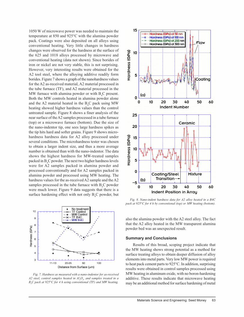
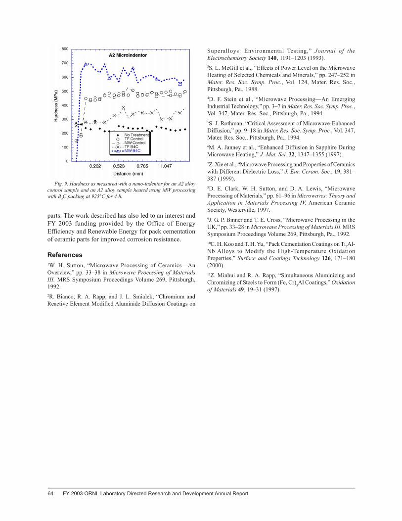
1050 W of microwave power was needed to maintain thetemperature at 850 and 925°C with the alumina powderpack. Coatings were also deposited on all alloys usingconventional heating. Very little changes in hardnesschanges were observed for the hardness at the surface ofthe 625 and 1018 alloys processed by microwave andconventional heating (data not shown). Since borides ofiron or nickel are not very stable, this is not surprising.However, very interesting results were obtained for theA2 tool steel, where the alloying additive readily formborides. Figure 7 shows a graph of the nanohardness valuesfor the A2 as-received material, A2 material processed inthe tube furnace (TF), and A2 material processed in theMW furnace with alumina powder or with B4C present.Both the MW controls heated in alumina powder aloneand the A2 material heated in the B4C pack using MWheating showed higher hardness values than the controluntreated sample. Figure 8 shows a finer analysis of thenear surface of the A2 samples processed in a tube furnace(top) or a microwave furnace (bottom). Due the size ofthe nano-indentor tip, one sees large hardness spikes asthe tip hits hard and softer grains. Figure 9 shows micro-hardness hardness data for A2 alloy processed underseveral conditions. The microhardness tester was chosento obtain a larger indent size, and thus a more averagenumber is obtained than with the nano-indentor. The datashows the highest hardness for MW-treated samplespacked in B4C powder. The next two higher hardness levelswere for A2 samples packed in alumina powder andprocessed conventionally and for A2 samples packed inalumina powder and processed using MW heating. Thehardness values for the as-received A2 sample and the A2samples processed in the tube furnace with B4C powderwere much lower. Figure 9 data suggests that there is asurface hardening effect with not only B4C powder, but
also the alumina powder with the A2 steel alloy. The factthat the A2 alloy heated in the MW transparent aluminapowder bed was an unexpected result.
Summary and ConclusionsResults of this broad, scoping project indicate that
the MW heating shows strong potential as a method forsurface treating alloys to obtain deeper diffusion of alloyelements into metal parts. Very low MW power is requiredto heat pack cement parts to 925°C. In addition, surprisingresults were obtained in control samples processed usingMW heating in aluminum oxide, with no boron-hardeningadditive. These results indicate that microwave heatingmay be an additional method for surface hardening of metal
Fig. 7. Hardness as measured with a nano-indentor for as-receivedA2 steel, control samples heated in Al2O3, and samples treated in aB4C pack at 925°C for 4 h using conventional (TF) and MW heating.
Fig. 8. Nano-indent hardness data for A2 alloy heated in a B4Cpack at 925°C for 4 h by conventional (top) or MW heating (bottom).
64 FY 2003 ORNL Laboratory Directed Research and Development Annual Report
parts. The work described has also led to an interest andFY 2003 funding provided by the Office of EnergyEfficiency and Renewable Energy for pack cementationof ceramic parts for improved corrosion resistance.
References1W. H. Sutton, “Microwave Processing of Ceramics—AnOverview,” pp. 33–38 in Microwave Processing of MaterialsIII. MRS Symposium Proceedings Volume 269, Pittsburgh,1992.2R. Bianco, R. A. Rapp, and J. L. Smialek, “Chromium andReactive Element Modified Aluminide Diffusion Coatings on
Fig. 9. Hardness as measured with a nano-indentor for an A2 alloycontrol sample and an A2 alloy sample heated using MW processingwith B4C packing at 925°C for 4 h.
Superalloys: Environmental Testing,” Journal of theElectrochemistry Society 140, 1191–1203 (1993).3S. L. McGill et al., “Effects of Power Level on the MicrowaveHeating of Selected Chemicals and Minerals,” pp. 247–252 inMater. Res. Soc. Symp. Proc., Vol. 124, Mater. Res. Soc.,Pittsburgh, Pa., 1988.4D. F. Stein et al., “Microwave Processing—An EmergingIndustrial Technology,” pp. 3–7 in Mater. Res. Soc. Symp. Proc.,Vol. 347, Mater. Res. Soc., Pittsburgh, Pa., 1994.5S. J. Rothman, “Critical Assessment of Microwave-EnhancedDiffusion,” pp. 9–18 in Mater. Res. Soc. Symp. Proc., Vol. 347,Mater. Res. Soc., Pittsburgh, Pa., 1994.6M. A. Janney et al., “Enhanced Diffusion in Sapphire DuringMicrowave Heating,” J. Mat. Sci. 32, 1347–1355 (1997).7Z. Xie et al., “Microwave Processing and Properties of Ceramicswith Different Dielectric Loss,” J. Eur. Ceram. Soc., 19, 381–387 (1999).8D. E. Clark, W. H. Sutton, and D. A. Lewis, “MicrowaveProcessing of Materials,” pp. 61–96 in Microwaves: Theory andApplication in Materials Processing IV, American CeramicSociety, Westerville, 1997.9J. G. P. Binner and T. E. Cross, “Microwave Processing in theUK,” pp. 33–28 in Microwave Processing of Materials III. MRSSymposium Proceedings Volume 269, Pittsburgh, Pa., 1992.10C. H. Koo and T. H. Yu, “Pack Cementation Coatings on Ti3Al-Nb Alloys to Modify the High-Temperature OxidationProperties,” Surface and Coatings Technology 126, 171–180(2000).11Z. Minhui and R. A. Rapp, “Simultaneous Aluminizing andChromizing of Steels to Form (Fe, Cr)3Al Coatings,” Oxidationof Materials 49, 19–31 (1997).
Materials Science and Engineering: Seed Money 65
Final Report Project Number: 3210-2038
Ultrasonic Processing of Ultrafine MaterialsQ. Han,1 C. L. Xu,2 G. R. Romanoski,1 D. T. Hoelzer,1 M. M. Menon,3 and R. P. Taleyarkhan4
1Metals and Ceramics Division2University of Tennessee
3Nuclear Science and Technology Division4Engineering Science and Technology Division
High-intensity ultrasonic energy can be used to produce oscillating strain/stress fields in solidmaterials. The purpose of this seed money project was to explore novel use of the strain/stress inducedby ultrasonic vibration for the production of ultrafine materials. Two new approaches have beendeveloped conceptually and tested experimentally. The first approach was to use ultrasonically inducedstrain/stress to induce plastic deformation in materials. The second approach was to use ultrasonicallyinduced oscillating stress fields to induce repeated phase transformation in the solid materials. Initialexperimental results indicate that, for the first time, nanostructures are formed in the ultrasonicallytreated metal. The size of the nanostructures obtained using the first approach is smaller than 200 nmand possibly in the range of 100 nm.
IntroductionNanostructured materials offer unique and entirely
different mechanical, electronical, optical, and magneticproperties compared with conventional micro- ormillimeter-sized materials. In metals, for example, thehardness of nanocrystalline copper increases withdecreasing grain size, and 6-nm copper grains show fivetimes the hardness of conventional copper.1 Nanosized Al-Ni-In alloys exhibit a tensile strength larger than1200 MPa, greater than conventional high-strengthaluminum alloys.2 Nanostructured M50 steel is morefatigue and fracture resistant than conventional M50 steelthat is widely used in the aircraft industry as the main-shaft bearings in gas turbine engines.3 In semiconductors,nanoclusters are often referred to as quantum dots,nanocrystals, and Q-particles. As an example, quantumdots can be developed to emit and absorb a desiredwavelength of light by changing the particle diameter. Thisfeature allows the construction of a finely tunable andefficient semiconductor laser.
Traditional methods for producing nanostructuredmaterials include gas atomization and ball milling,followed by consolidation and rapid solidification.4–6
These processes tend to be expensive and capable ofproducing only small amounts of material. Recentlyapproaches for producing nanostructured materials includesevere plastic deformation.7–8 equal channel angularextrusion (ECAE) is one of the methods that uses severeplastic deformation to produce nanostructured materials,but the size of the sample is limited due to the high friction
forces that exist between the material and the wall.9 Thesedevelopments suggest that methods that can producesevere plastic deformation have the potential in theproduction of nanostructured materials.
Ultrasonic vibrations produce oscillating strain andstress fields in solid materials.10 Experiments have shownthat ultrasonic vibrations above a critical intensity increasethe concentration of dislocations and point defects in thesolids. The density of the defects increases with increasingultrasonic intensity. When the density of the dislocationsis high enough, an alignment of dislocations occurs. It hasbeen observed that a distinct cellular structure, about 2µm in size, is formed in ultrasonically treated aluminummonocrystals after it was exposed to ultrasonic vibrationfor only 8 s.11 The experimental evidence suggests thatultrasound is a powerful tool in producing severe plasticdeformation in solid materials. However, the grains sizewas still a few orders of magnitude larger than the size ofnanostructures. Also the oscillating nature of the strainand stress induced in solid metal by ultrasonic vibrationsis not explored for grain refinement.
The purpose of this research was to investigate thepossibility of producing nanostructures in metals usingultrasonic vibrations. Two new approaches have beendeveloped conceptually and tested experimentally. Initialexperimental results indicate that, for the first time,nanostructures are formed in the ultrasonically treatedmetal. The size of the nanostructures obtained using thefirst approach is smaller than 200 nm and possibly in therange of 100 nm.
66 FY 2003 ORNL Laboratory Directed Research and Development Annual Report
Technical ApproachThe First Approach
The idea in the first approach was to use theultrasonically induced strain/stress to enhance dislocationand vacancy densities in metal in the hope that the line/point defects can align themselves to form ultra-finestructures. Extruded 1010 steel was used, and the initialgrain size in the steel was about 10 µm. A 20-kHz, 1.5-kW ultrasonic unit was used for the experiments. Initiallyultrasonic energy was directly injected into steel bars. Nosubstantial grain refinement was observed, and the barfractured due to fatigue. This was because in an oscillatingstress field, the stresses are periodic (positive andnegative). Usually materials fracture more easily undertensile stress.
A novel approach was then developed to offset theinstantaneous tensile stress induced by ultrasonic vibration.High-intensity ultrasonic energy was then focused onspecific locations in the specimen for 60 s, resulting in asevere plastic deformation in those locations. Thedeformed region was polished, etched, and characterizedusing scanning electron microscopy (SEM) andtransmission electron microscopy (TEM).
The Second ApproachThe idea in the second approach was to inject acoustic
energy into metal at its solid/solid phase transformationtemperature such that the oscillating stress generated byultrasonic vibration may lead to a repeated phasetransformation at high frequency. The solid/solid phasetransformation temperature varies with external stress.Under the influence of oscillating stress, the phasetransformation temperature will also oscillate around itsequilibrium temperature. When the specimen underacoustic vibration is held at the equilibrium solid/solidphase transformation temperature, oscillating undercoolingoccurs for both phases, which may result in repeatednucleation for both of the phases involved. Since thediffusion coefficient in the solid state is very small, thegrowth rate of the newly formed phase will be small, andthe grain size of the newly formed phase will be mainlydetermined by the nucleation stage of the phasetransformation.
In the second approach, bar specimens were madeout of 1010 steel and placed in a furnace with a knowntemperature gradient. The temperature was 1000°C at oneend of the specimen and was room temperature at the otherend to ensure that the α to γ phase transformation occurredat a certain location in the specimen. Ultrasonic energywas then injected into the specimen for 5 to 20 s until thespecimen was quenched in water to preserve the grain sizeat high temperatures.
Results and AccomplishmentsUltrasonically Induced Plastic Deformation
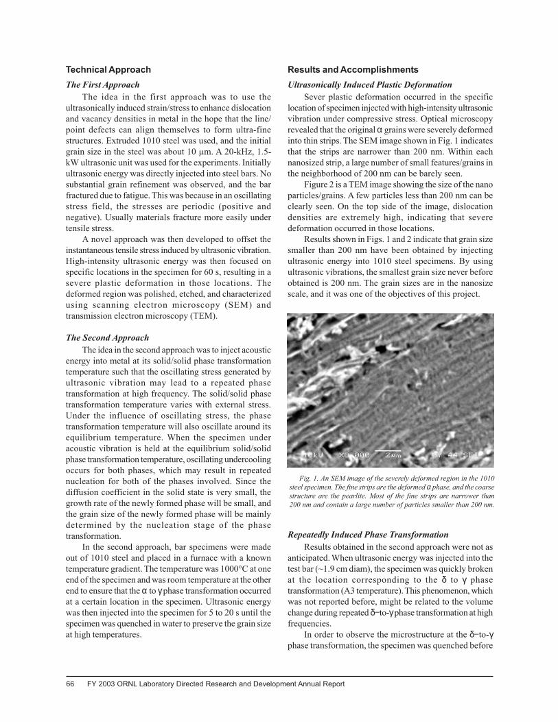
Sever plastic deformation occurred in the specificlocation of specimen injected with high-intensity ultrasonicvibration under compressive stress. Optical microscopyrevealed that the original α grains were severely deformedinto thin strips. The SEM image shown in Fig. 1 indicatesthat the strips are narrower than 200 nm. Within eachnanosized strip, a large number of small features/grains inthe neighborhood of 200 nm can be barely seen.
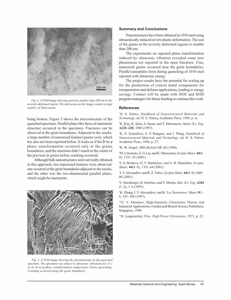
Figure 2 is a TEM image showing the size of the nanoparticles/grains. A few particles less than 200 nm can beclearly seen. On the top side of the image, dislocationdensities are extremely high, indicating that severedeformation occurred in those locations.
Results shown in Figs. 1 and 2 indicate that grain sizesmaller than 200 nm have been obtained by injectingultrasonic energy into 1010 steel specimens. By usingultrasonic vibrations, the smallest grain size never beforeobtained is 200 nm. The grain sizes are in the nanosizescale, and it was one of the objectives of this project.
Repeatedly Induced Phase TransformationResults obtained in the second approach were not as
anticipated. When ultrasonic energy was injected into thetest bar (~1.9 cm diam), the specimen was quickly brokenat the location corresponding to the δ to γ phasetransformation (A3 temperature). This phenomenon, whichwas not reported before, might be related to the volumechange during repeated δ−to-γ phase transformation at highfrequencies.
In order to observe the microstructure at the δ−to-γphase transformation, the specimen was quenched before
Fig. 1. An SEM image of the severely deformed region in the 1010steel specimen. The fine strips are the deformed α phase, and the coarsestructure are the pearlite. Most of the fine strips are narrower than200 nm and contain a large number of particles smaller than 200 nm.
Materials Science and Engineering: Seed Money 67
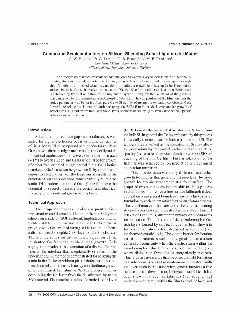
being broken. Figure 3 shows the microstructure of thequenched specimen. Parallel plates like those of martensitestructure occurred in the specimen. Fractures can beobserved at the grain boundaries. Adjacent to the cracks,a large number of nanosized features/grains exist, whichhas also not been reported before. It looks as if the δ−to-γphase transformation occurred only at the grainsboundaries, and the reactions didn’t reach to the center ofthe previous α grains before cracking occurred.
Although bulk nanostructures were not really obtainedin this approach, two nanosized features were observed:one occurred at the grain boundaries adjacent to the cracks,and the other was the two-dimensional parallel plates,which might be martensite.
Fig. 2. A TEM image showing particles smaller than 200 nm in theseverely deformed region. The dark areas on the image contain a largenumber of dislocations.
Fig. 3. A TEM image showing the microstructure in the quenchedspecimen. The specimen was subject to ultrasonic vibrations for 15 sat its α−to-γ phase transformation temperature before quenching.Cracking occurred along the grain boundaries.
Summary and ConclusionsNanostructures have been obtained in 1010 steel using
ultrasonically induced severe plastic deformation. The sizeof the grains in the severely deformed regions is smallerthan 200 nm.
The experiments on repeated phase transformationinduced by ultrasonic vibration revealed some newphenomena not reported in the open literature. Fine,nanosized grains occurred near the grain boundaries.Parallel nanoplates form during quenching of 1010 steelinjected with ultrasonic energy.
The project results have the potential for scaling upfor the production of critical metal components fortransportation and defense applications, leading to energysavings. Contact will be made with DOE and DODprogram managers for future funding to continue this work.
References1H. S. Nalwa, Handbook of Nanostructured Materials andTechnology, ed. H. S. Nalwa, Academic Press, 1996, p. ix.2K. Kita, K. Saito, A. Inoue, and T. Matsumoto, Mater. Sci. Eng.A226–228, 1004 (1997).3K. E. Gonsalves, S. P. Rangara, and J. Wang, Handbook ofNanostructured Materials and Technology, ed. H. S. Nalwa,Academic Press, 1996, p. 27.4R. W. Seigel, MRS Bulletin 15, 60 (1990).5M. Umemoto, Z. G. Liu, and K. Masuyama, Scripta Mater. 44(8–9), 1741–45 (2001).6I. G. Brodova, D. V. Bashlykov, and A. B. Manukhin, Scripta.Mater. 44(8–9), 1761–64 (2001).7I. V. Alexandrov and R. Z. Valiev, Scripta Mater. 44(8–9), 1605–08 (2001).8I. Altenburger, B. Scholtes, and V. Martin, Mat. Sci. Eng. A264(1–2), 1–6 (1991).9K. Zhang, I. V. Alexandrov, and K. Lu, Nanostruct. Mater. 9(1–8, 347–350 (1997).10O. V. Abramov, High-Intensity Ultrasonics Theory andIndustrial Applications, Gorden and Breach Science Publishers,Singapore, 1998.11B. Langenecker, Proc. High Power Ultrasonics, 1971, p. 32.
68 FY 2003 ORNL Laboratory Directed Research and Development Annual Report
Final Report Project Number 3210-2039
Compound Semiconductors on Silicon: Shedding Some Light on the MatterO. W. Holland,1 B. C. Larson,1 D. B. Beach,2 and M. F. Chisholm1
1Condensed Matter Sciences Division2Chemical and Analytical Sciences Division
The integration of lattice-mismatched material onto Si wafers is key to increasing the functionalityof integrated circuits and, in particular, to integrating both optical and digital processing on a singlechip. A method is proposed which is capable of providing a growth template on Si for films with alattice mismatch of ≤4%. It involves implantation of Ge into Si to form a dilute solid solution. Enrichmentis achieved by thermal oxidation of the implanted layer to snowplow the Ge ahead of the growingoxide interface to form a uniform pseudomorphic SiGe film. The composition of the film (and thus thelattice parameter) can be varied from pure Ge to Si rich by adjusting the oxidation conditions. Onceformed and relaxed to its natural lattice spacing, the SiGe film is an ideal template for growth ofdefect-free GaAs and/or strained-layer SiGe layers. Methods of achieving this relaxation without plasticdeformation are discussed.
IntroductionSilicon, an indirect bandgap semiconductor, is well
suited for digital electronics but is an inefficient emitterof light. Many III-V compound semiconductors such asGaAs have a direct bandgap and, as such, are ideally suitedfor optical applications. However, the lattice mismatch(4.1%) between silicon and GaAs is too large for growthof defect-free, oriented, single-crystal films. Ge is latticematched to GaAs and can be grown on Si by a number ofdeposition techniques, but the large misfit results in thecreation of misfit dislocations, which partially relieve thestrain. Dislocations that thread through the film have thepotential to severely degrade the optical and electricalintegrity of any material grown on this layer.
Technical ApproachThe proposed process involves sequential Ge+-
implantation and thermal oxidation of the top Si layer insilicon-on-insulator (SOI) material. Implantation initiallyyields a dilute SiGe mixture in the near surface that isprogressively Ge enriched during oxidation until it formsa distinct pseudomorphic GeSi-layer on the Si substrate.The method relies on the complete rejection of theimplanted Ge from the oxide during growth. Thissegregation results in the formation of a distinct Ge-richlayer at the interface that is epitaxially oriented on theunderlying Si. A method is demonstrated for relaxing thestrain in the Ge layer without plastic deformation so thatit can be used as an intermediate layer to facilitate growthof lattice mismatched films on Si. The process involvesdecoupling the Ge layer from the Si substrate by usingSOI material. The material consists of a buried oxide layer
(BOX) beneath the surface that isolates a top Si layer fromthe bulk Si. In general the Ge layer formed by this processis biaxially strained near the lattice parameter of Si. Thetemperatures involved in the oxidation of Si may allowthe germanium layer to partially relax to its natural latticespacing (i.e., as a result of viscoelastic flow of the SiO2 orbuckling of the thin Ge film). Further relaxation of thefilm has was achieved by ion irradiation without misfitdislocation formation.
This process is substantially different from othergrowth techniques that generally achieve layer-by-layergrowth by atomic attachment at a free surface. Theproposed two-step process is more akin to a bulk processin that it does not involve a free surface (although it doesdepend on a interfacial boundary), and it achieves layerformation by enrichment rather than by an adatom process.These differences offer substantial benefits in formingstrained layers that yield a greater thermal stability (againstrelaxation) and, thus, different pathways or mechanismsfor relaxation. The thickness of the pseudomorphic Ge-rich layers formed by this technique has been shown tofar exceed the critical value established by Matthew1 (i.e.,the thermodynamic limit). The kinetic barrier for formingmisfit dislocations is sufficiently great that relaxationgenerally occurs only when the elastic strain within thepseudomorphic film far exceeds its critical value (i.e.,where dislocation formation is energetically favored).Thus, studies have shown that the onset of misfit formationcan only occur as a result of nonhomogeneous strain withthe layer. Such is the cause when growth involves a freesurface that can develop morphological instabilities. It hasbeen shown that such instabilities (i.e., roughening)redistribute the strain within the film to produce localized
Materials Science and Engineering: Seed Money 69
strain that is capable of nucleating misfit growth. Thus,the absence of a free surface and the inherent stabilityagainst roughening in the layers formed by the proposedtechnique is considered to be responsible for its substantialbenefits over other techniques.
Results and AccomplishmentsCross-section, transmission electron micrographs
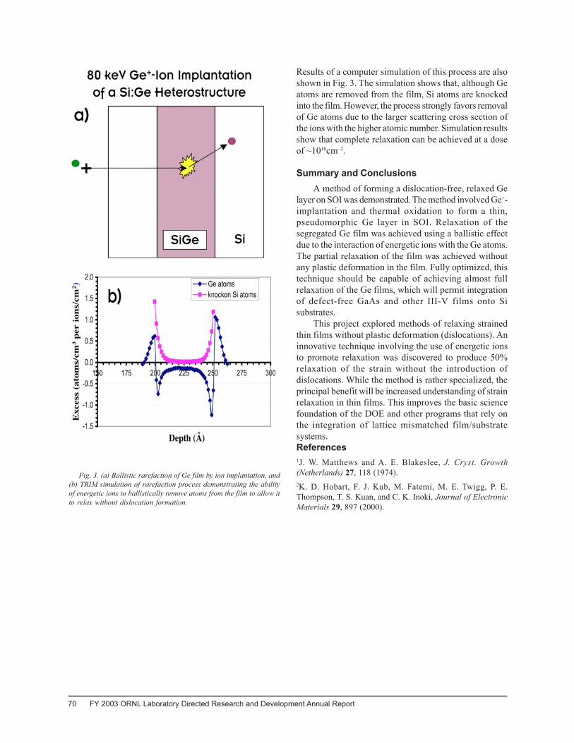
(XTEM) in Fig. 1 show a SiGe film formed by thistechnique. The sample shown is an SOI wafer implantedwith Ge at 80 keV at a dose of 5 × 1016cm–2. It was oxidizedin dry O2 in several stages. An initial cycle of 1150°C/3 hwas used followed by a 1050°C cycle and a final cycle at930°C. The oxidation temperature was decreased as theGe content of the film increases to avoid melting (whichoccurs at 934°C for pure Ge). These oxidation cyclesremoved most of the top Si layer and left only a well-defined SiGe layer encapsulated between the thermal oxide(on the top) and the buried oxide (BOX) of the SOI. Boththe bright-field image in Fig. 1(a) and the dark-field imagein Fig.1(b) demonstrate that partial relaxation of the film(~50%) has occurred by dislocation formation.Interestingly, both micrographs indicate that the segregatedfilm has bifurcated into a Ge-rich layer at the top and a Si-rich layer at the bottom. Threading dislocation segmentscan be seen originating from the bilayer interface. Theresults demonstrate that the viscoelastic response of theBOX is insufficient to accommodate the strain in the SiGefilm. These results are consistent with those by Hobart,2
who reported relaxation in a compressively strained SiGefilm bonded to a borophosphorosilicate glass by buckling.
Buckling was avoided by patterning the film into smallareas prior to annealing (i.e., relaxation).
It is clear that another technique is required to achievedefect-free relaxation of the segregated film. XTEM of asample that was processed similarly to the one previouslydiscussed is shown in Fig. 2. It is clear from the figurethat the SiGe film (estimated to be 70% Ge) is quiteuniform in thickness with planar interfaces at both oxidelayers. There is no indication of bifurcation within the film.An inspection across the entire field of view (~severalmicrons) within the microscope failed to find anydislocations within the film. This yields a rough estimatefor the upper limit for threading dislocations density of~107 cm–2. The main difference in processing of this samplecompared to the one shown in Fig. 1 was that it wasirradiated (with 200 keV Si+ ions) prior to the finaloxidation cycle at 900°C in an attempt to promoterelaxation within the Ge layer. While no additionalrelaxation was observed compared to a non-irradiatedcontrol, the ion mixed sample achieved a 50% relaxationof the in-plane spacing without plastic deformation (i.e.,no misfit dislocations), while a high dislocation densitywas observed in the control sample.
The use of energetic ions to promote relaxation ofhighly strained, pseudomorphic films offers an innovativemethod to form dislocation-free, relaxed films. The effectderives from the ability of the energetic ions to transfersufficient energy to the Ge atoms in the film to physicallyremove them from the film. This ballistic effect is shownpictorially in Fig. 3. The biaxial compressed film is relaxedby the physical removal of excess Ge atoms in the film,which allows the film to relax to its natural lattice spacing.
Fig. 1. XTEM micrograph of a Ge-rich film encapsulated within aSOI material by a buried oxide (BOX) and a superficial thermal oxideat the surface. The SOI was implanted with 80 keV Ge+-ions at a fluenceof 5 × 1016cm–2. (a) Bright field image revealing a dislocation arraynear the centerline of the film with threading segments spanning tothe top and bottom interface. (b) z-contrast image showing bilayer:top 24 nm of film is Ge rich compared to bottom 16 nm. Viscoelasticresponse of the oxide substrate (BOX) is insufficient for large areafilms to achieve defect-free relaxation of the encapsulated film. Strainrelaxation is observed, but it appears to be predominantly due to misfitdislocation formation.
Fig. 2. XTEM of a continuous 15 nm Si0.3Ge0.7 film with nodislocations by inspection over a wide area.
70 FY 2003 ORNL Laboratory Directed Research and Development Annual Report
Results of a computer simulation of this process are alsoshown in Fig. 3. The simulation shows that, although Geatoms are removed from the film, Si atoms are knockedinto the film. However, the process strongly favors removalof Ge atoms due to the larger scattering cross section ofthe ions with the higher atomic number. Simulation resultsshow that complete relaxation can be achieved at a doseof ~1016cm–2.
Summary and ConclusionsA method of forming a dislocation-free, relaxed Ge
layer on SOI was demonstrated. The method involved Ge+-implantation and thermal oxidation to form a thin,pseudomorphic Ge layer in SOI. Relaxation of thesegregated Ge film was achieved using a ballistic effectdue to the interaction of energetic ions with the Ge atoms.The partial relaxation of the film was achieved withoutany plastic deformation in the film. Fully optimized, thistechnique should be capable of achieving almost fullrelaxation of the Ge films, which will permit integrationof defect-free GaAs and other III-V films onto Sisubstrates.
This project explored methods of relaxing strainedthin films without plastic deformation (dislocations). Aninnovative technique involving the use of energetic ionsto promote relaxation was discovered to produce 50%relaxation of the strain without the introduction ofdislocations. While the method is rather specialized, theprincipal benefit will be increased understanding of strainrelaxation in thin films. This improves the basic sciencefoundation of the DOE and other programs that rely onthe integration of lattice mismatched film/substratesystems.References1J. W. Matthews and A. E. Blakeslee, J. Cryst. Growth(Netherlands) 27, 118 (1974).2K. D. Hobart, F. J. Kub, M. Fatemi, M. E. Twigg, P. E.Thompson, T. S. Kuan, and C. K. Inoki, Journal of ElectronicMaterials 29, 897 (2000).
Fig. 3. (a) Ballistic rarefaction of Ge film by ion implantation, and(b) TRIM simulation of rarefaction process demonstrating the abilityof energetic ions to ballistically remove atoms from the film to allow itto relax without dislocation formation.
Materials Science and Engineering: Seed Money 71
Final Report Project Number: 3210-2049
Ferromagnetism in Dilute Magnetic Semiconductors: Getting to theScience with Neutron Scattering
B. C. Sales,1 D. Mandrus,1 H. A. Mook, Jr.,1 L. A. Boatner,1 and T. C. Schulthess2
1Condensed Matter Sciences Division2Computer Science and Mathematics Division
This project focused on the growth and characterization of single crystals of dilute magneticsemiconductors (DMS). DMS are one of the key components in the next generation of electronicdevices that make use of the electron spin as well as its charge. The origin of the ferromagnetism inDMS is not well understood, in part because virtually all of the DMS have been prepared in thin filmform using nonequilibrium synthesis methods. Single crystals can be studied with a larger variety ofexperimental methods, including neutron scattering. A large number of magnetically doped singlecrystals were prepared during the early stages of this project (chalcopyrites, ZnO, KTaO3, Ge, andTiO2—doped with Mn, Co, and Fe). Initial studies on these crystals indicated that much of the room-temperature ferromagnetism reported in the literature was due to clustering and/or an impurity phase.To avoid clustering, we have grown and started to characterize large crystals (≈0.7 g) of a stochiometricDMS: Yb14MnSb11. In this ferromagnetic compound, all of the Mn atoms are located at a well-definedcrystallographic site, and hence there is no problem with clustering. Yb14MnSb11 and related compoundsappear to be ideal materials on which to unravel the magnetism in DMS. Because of the extra workinvolved in showing that earlier studies were incorrect, neutron scattering experiments were notconducted as part of this seed money. However, the Yb14MnSb11 materials were shown to be extremelyinteresting and DOE Basic Energy Sciences funding has been redirected to fund neutron scatteringexperiments that are currently in progress.
Introduction“Until recently, the spin of the electron was ignored
in mainstream charge-based electronics. A technology hasemerged called spintronics (spin transport electronics orspin based electronics), where it is not the electron chargebut the electron spin that carries information, and this offersopportunities for a new generation of devices combiningstandard microelectronics with spin-dependent effects thatarise from the interaction between the spin of the carrierand the magnetic properties of the material.”1 This quotefrom a recent review article in Science summarizes theemerging field of spintronics that includes everything fromspin valves to quantum computing. This is a vast new areaof science and technology that has already resulted in newread heads for computer hard drives (based on a spinvalve)1 and the first demonstration of a primitive quantumcomputer.2
One of the key components in the next generation ofproposed spintronic devices is a ferromagneticsemiconductor that can be used as a source of current inwhich the spins of the carriers are highly polarized.1,3 Therecent observation of ferromagnetism near roomtemperature in semiconductors containing a few percentof magnetic atoms was a surprise and is not well
understood.4,5 To date, all of the DMS have been preparedin thin-film form using nonequilibrium synthesis methods.Neutron scattering is the most powerful technique forprobing and understanding magnetism in a solid, but itdoes not have enough sensitivity to study a DMS thin film.The goal of this project is to identify and prepare one ormore DMS as a large single crystal (>1 mm3) suitable forneutron scattering investigations.
Technical ApproachA large number of different materials were grown as
single crystals based on various reports in the literature.These reports usually indicated the observation offerromagnetism in a thin-film semiconductor doped witha few percent of a magnetic element such as Co, Mn, orFe via a nonequilibrium method. Based on these reports,we prepared crystals of the following materials:1. ZnO doped with Mn or Co (Crystals were grown via
vapor transport in a sealed silica tube at temperaturesbetween 600–800°C using NH4Cl as a transportagent.)
2. Ge doped with Mn (Crystals grown by slow coolingof melt in a silica crucible from 1100°C or byquenching the melt to room temperature followed byannealing.)
72 FY 2003 ORNL Laboratory Directed Research and Development Annual Report
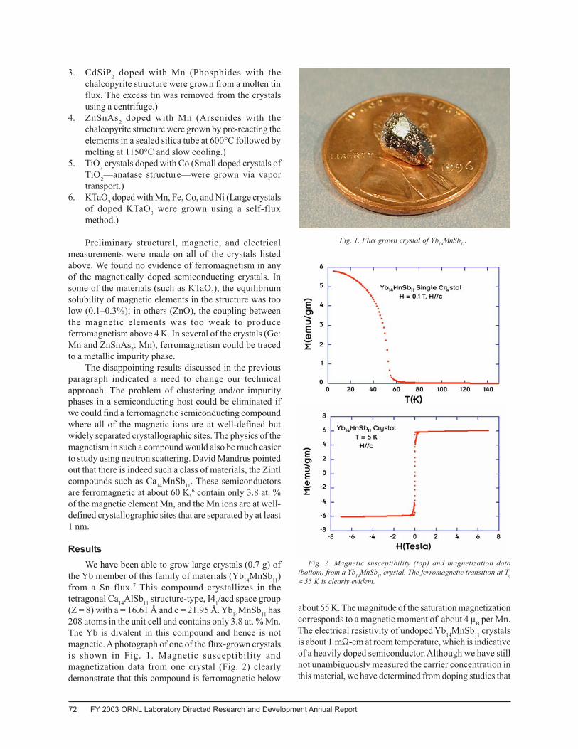
Fig. 2. Magnetic susceptibility (top) and magnetization data(bottom) from a Yb14MnSb11 crystal. The ferromagnetic transition at Tc≈ 55 K is clearly evident.
3. CdSiP2 doped with Mn (Phosphides with thechalcopyrite structure were grown from a molten tinflux. The excess tin was removed from the crystalsusing a centrifuge.)
4. ZnSnAs2 doped with Mn (Arsenides with thechalcopyrite structure were grown by pre-reacting theelements in a sealed silica tube at 600°C followed bymelting at 1150°C and slow cooling.)
5. TiO2 crystals doped with Co (Small doped crystals ofTiO2—anatase structure—were grown via vaportransport.)
6. KTaO3 doped with Mn, Fe, Co, and Ni (Large crystalsof doped KTaO3 were grown using a self-fluxmethod.)
Preliminary structural, magnetic, and electricalmeasurements were made on all of the crystals listedabove. We found no evidence of ferromagnetism in anyof the magnetically doped semiconducting crystals. Insome of the materials (such as KTaO3), the equilibriumsolubility of magnetic elements in the structure was toolow (0.1–0.3%); in others (ZnO), the coupling betweenthe magnetic elements was too weak to produceferromagnetism above 4 K. In several of the crystals (Ge:Mn and ZnSnAs2: Mn), ferromagnetism could be tracedto a metallic impurity phase.
The disappointing results discussed in the previousparagraph indicated a need to change our technicalapproach. The problem of clustering and/or impurityphases in a semiconducting host could be eliminated ifwe could find a ferromagnetic semiconducting compoundwhere all of the magnetic ions are at well-defined butwidely separated crystallographic sites. The physics of themagnetism in such a compound would also be much easierto study using neutron scattering. David Mandrus pointedout that there is indeed such a class of materials, the Zintlcompounds such as Ca14MnSb11. These semiconductorsare ferromagnetic at about 60 K,6 contain only 3.8 at. %of the magnetic element Mn, and the Mn ions are at well-defined crystallographic sites that are separated by at least1 nm.
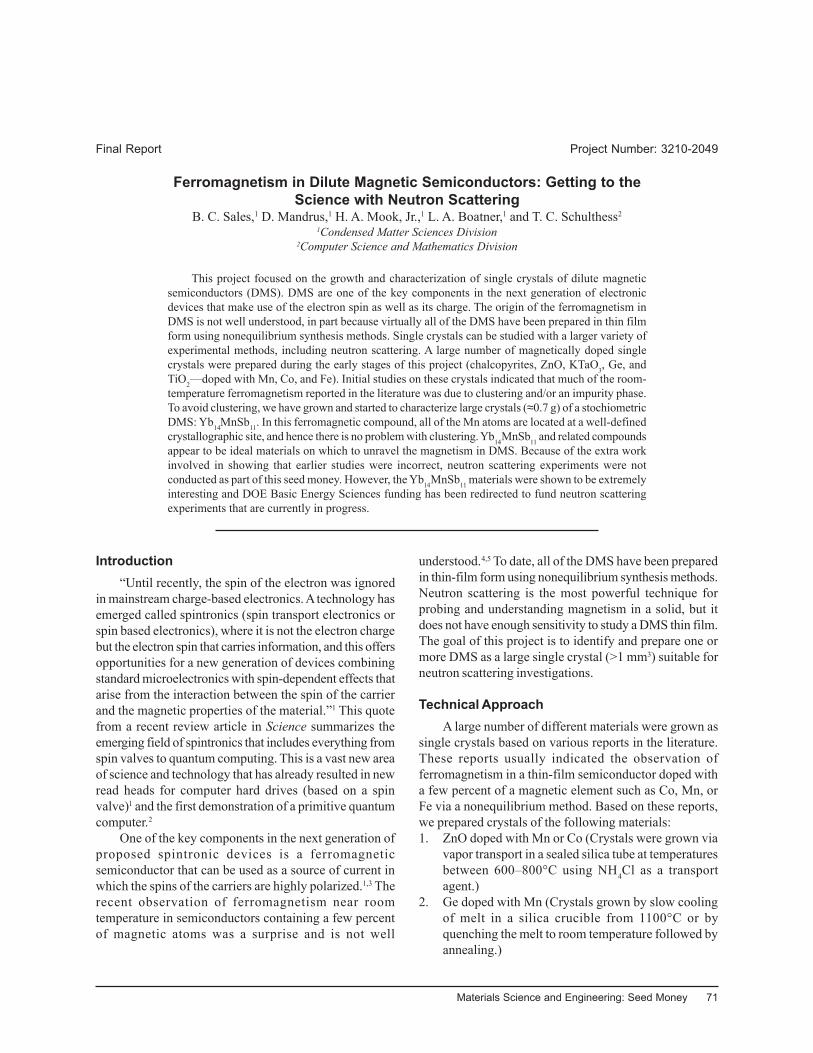
ResultsWe have been able to grow large crystals (0.7 g) of
the Yb member of this family of materials (Yb14MnSb11)from a Sn flux.7 This compound crystallizes in thetetragonal Ca14AlSb11 structure-type, I41/acd space group(Z = 8) with a = 16.61 Å and c = 21.95 Å. Yb14MnSb11 has208 atoms in the unit cell and contains only 3.8 at. % Mn.The Yb is divalent in this compound and hence is notmagnetic. A photograph of one of the flux-grown crystalsis shown in Fig. 1. Magnetic susceptibility andmagnetization data from one crystal (Fig. 2) clearlydemonstrate that this compound is ferromagnetic below
Fig. 1. Flux grown crystal of Yb14MnSb11.
about 55 K. The magnitude of the saturation magnetizationcorresponds to a magnetic moment of about 4 µB per Mn.The electrical resistivity of undoped Yb14MnSb11 crystalsis about 1 mΩ-cm at room temperature, which is indicativeof a heavily doped semiconductor. Although we have stillnot unambiguously measured the carrier concentration inthis material, we have determined from doping studies that
Materials Science and Engineering: Seed Money 73
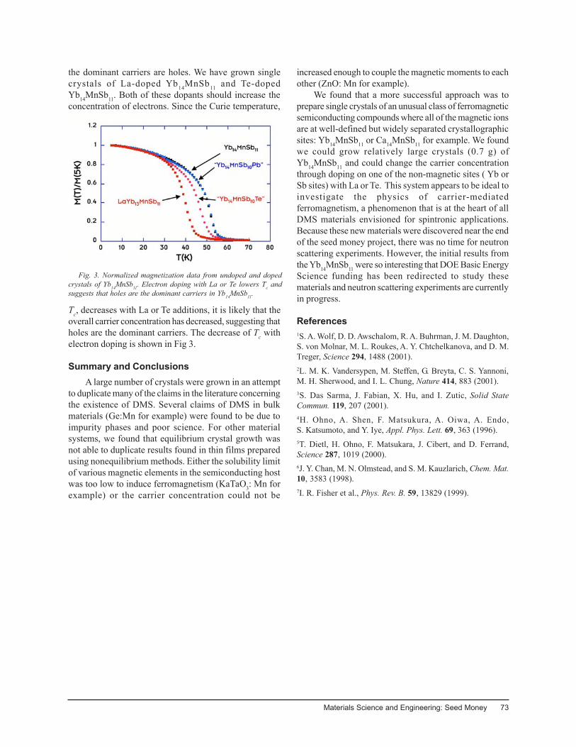
Fig. 3. Normalized magnetization data from undoped and dopedcrystals of Yb14MnSb11. Electron doping with La or Te lowers Tc andsuggests that holes are the dominant carriers in Yb14MnSb11.
the dominant carriers are holes. We have grown singlecrystals of La-doped Yb14MnSb11 and Te-dopedYb14MnSb11. Both of these dopants should increase theconcentration of electrons. Since the Curie temperature,
Tc, decreases with La or Te additions, it is likely that theoverall carrier concentration has decreased, suggesting thatholes are the dominant carriers. The decrease of Tc withelectron doping is shown in Fig 3.
Summary and ConclusionsA large number of crystals were grown in an attempt
to duplicate many of the claims in the literature concerningthe existence of DMS. Several claims of DMS in bulkmaterials (Ge:Mn for example) were found to be due toimpurity phases and poor science. For other materialsystems, we found that equilibrium crystal growth wasnot able to duplicate results found in thin films preparedusing nonequilibrium methods. Either the solubility limitof various magnetic elements in the semiconducting hostwas too low to induce ferromagnetism (KaTaO3: Mn forexample) or the carrier concentration could not be
increased enough to couple the magnetic moments to eachother (ZnO: Mn for example).
We found that a more successful approach was toprepare single crystals of an unusual class of ferromagneticsemiconducting compounds where all of the magnetic ionsare at well-defined but widely separated crystallographicsites: Yb14MnSb11 or Ca14MnSb11 for example. We foundwe could grow relatively large crystals (0.7 g) ofYb14MnSb11 and could change the carrier concentrationthrough doping on one of the non-magnetic sites ( Yb orSb sites) with La or Te. This system appears to be ideal toinvestigate the physics of carrier-mediatedferromagnetism, a phenomenon that is at the heart of allDMS materials envisioned for spintronic applications.Because these new materials were discovered near the endof the seed money project, there was no time for neutronscattering experiments. However, the initial results fromthe Yb14MnSb11 were so interesting that DOE Basic EnergyScience funding has been redirected to study thesematerials and neutron scattering experiments are currentlyin progress.
References1S. A. Wolf, D. D. Awschalom, R. A. Buhrman, J. M. Daughton,S. von Molnar, M. L. Roukes, A. Y. Chtchelkanova, and D. M.Treger, Science 294, 1488 (2001).2L. M. K. Vandersypen, M. Steffen, G. Breyta, C. S. Yannoni,M. H. Sherwood, and I. L. Chung, Nature 414, 883 (2001).3S. Das Sarma, J. Fabian, X. Hu, and I. Zutic, Solid StateCommun. 119, 207 (2001).4H. Ohno, A. Shen, F. Matsukura, A. Oiwa, A. Endo,S. Katsumoto, and Y. Iye, Appl. Phys. Lett. 69, 363 (1996).5T. Dietl, H. Ohno, F. Matsukara, J. Cibert, and D. Ferrand,Science 287, 1019 (2000).6J. Y. Chan, M. N. Olmstead, and S. M. Kauzlarich, Chem. Mat.10, 3583 (1998).7I. R. Fisher et al., Phys. Rev. B. 59, 13829 (1999).
74 FY 2003 ORNL Laboratory Directed Research and Development Annual Report
Final Report Project Number: 3210-2053
Growth of MgB2 Thin Films for Superconductor ApplicationsT. M. Besmann, A. Goyal, and D. M. Kroeger
Metals and Ceramics Division
The recent discovery of the superconducting properties of MgB2 has stirred significant scientificand technological interest. Films of MgB2 have potential advantages over oxide superconductors intheir applicability to Josephson Junctions and as high-power, medium-temperature superconductorwires and tapes. A major issue in the use of the material is its fabrication in a cost-effective manner.While a number of attempts to produce films have been successful, they all use very expensive, low-throughput techniques such as laser ablation. We proposed to use a unique chemical vapor deposition(CVD) precursor system that would allow, for the first time, the deposition of the MgB2 phase usingthis technique. Resources were sufficient to prepare the CVD for the deposition of MgB2 using twounique precursors, and for a limited number (5) of runs. The films were characterized with regard totheir crystallinity and composition. It was determined that MgB2 was not formed under the conditionsutilized, although elemental magnesium was deposited. This was encouraging for future attempts, aswell as valuable in itself.
IntroductionThe recent discovery of superconductivity in
magnesium diboride, MgB2, by Akimitsu et al. caused aflurry of activity among researchers all over the world.1,2
MgB2 is a simple binary intermetallic compound with atransition temperature, Tc, of 39 K. This value is nearlytwice that of any previously known metallicsuperconductor. Bud’ko et al.3 demonstrated a boronisotope effect in Mg10B2 with an increase of Tc to 40.2 Kand concluded that the compound behaves as a phonon-mediated BCS superconductor. The growth of thin filmsof MgB2 with Tc near 39 K and with critical currentdensities greater than 105 A/cm2 has been reported.
The problem in growing high-quality MgB2 films insitu using physical vapor deposition techniques is that thevery high vapor pressure and volatility of magnesium inthe temperature range suitable for formation of MgB2(850–900°C) results in magnesium-deficient films. Hence,investigations have focused on using an ex situ approachso far. Such investigations use a two-step approach whereina boron precursor film is first deposited on the substrateand then the sample is annealed in a magnesium-containingenvironment. Zeng et al.4 have very recently reported ahigh-pressure chemical vapor deposition (CVD) in whichthey bulk heat magnesium to provide the vapor sourceand react it with diborane. Besides the tremendous toxicityof diborane, the use of high pressures is problematic inthat deposition on desired surfaces is difficult to control.Here, we propose to use a new method to fabricate high-quality MgB2 films—metalorganic CVD (MOCVD),which may be useful for both epitaxial and nonepitaxial
potential applications. Very recent reports from thePennsylvania State University confirm that a quasi-CVDapproach can produce high-quality MgB2 films, althoughthe boron source and volatility of the magnesium are stillproblematic.3
Technical ApproachThis project used the organometallics bis-
(cyclopentadienyl)-magnesium (Cp2Mg) as the magnesiumsource and o-carborane, o-C2H2B10H10, as the boron sourceand were commercially available from Aldrich, Inc. Therequired CVD equipment was available in our laboratory.
The efforts focused on the conditions needed toproduce dense, uniform coatings of ~0.2–1 µm in thicknesson various single-crystal substrates of interest such asC-plane sapphire. Variables that were explored centeredon the evaporation temperatures of the organometallicsources. Because of the differing thermochemical stabilityof the organometallics employed, different evaporationtemperatures at the same pressure are possible. Argoncarrier gas was used to deliver precursor molecules intothe reaction zone. As Cp2Mg is an air-sensitive compound,it required specialized handling, including the use of glovebags.
A set of evaporation temperatures for Cp2Mg ando-carborane temperatures were explored to deposit MgB2films. The films were characterized with respect tocrystallinity, composition, and microstructure usingelectron microscopy/scanning Auger spectroscopy and X-ray diffraction.
Materials Science and Engineering: Seed Money 75
Results and AccomplishmentsA CVD system was modified to accept the
organometallic precursor source vessels. The precursorswere acquired and were installed in the deposition system.The entire system was tested for leak-tightness and thermalstability. Since the vapor pressures of the precursors wereunknown, the range of vapor source temperatures had tobe estimated. These resulted in an apparent high rate ofevaporation of the o-carborane and a more modestevaporation rate of the magnesium precursor.
Five runs at various temperatures and flows wereperformed and are summarized in Table 1.
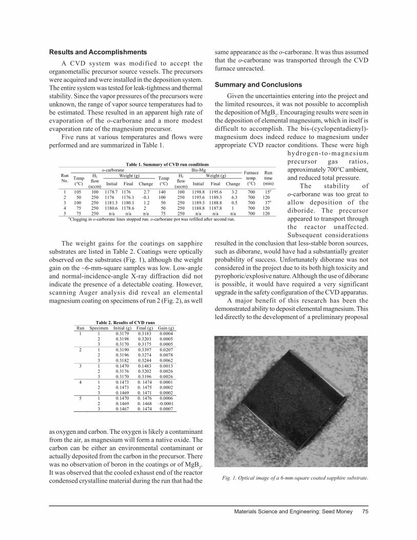
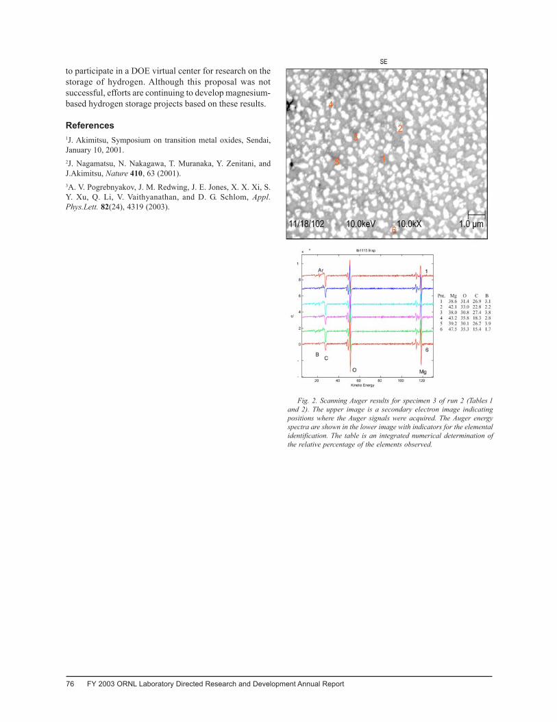
The weight gains for the coatings on sapphiresubstrates are listed in Table 2. Coatings were opticallyobserved on the substrates (Fig. 1), although the weightgain on the ~6-mm-square samples was low. Low-angleand normal-incidence-angle X-ray diffraction did notindicate the presence of a detectable coating. However,scanning Auger analysis did reveal an elementalmagnesium coating on specimens of run 2 (Fig. 2), as well
as oxygen and carbon. The oxygen is likely a contaminantfrom the air, as magnesium will form a native oxide. Thecarbon can be either an environmental contaminant oractually deposited from the carbon in the precursor. Therewas no observation of boron in the coatings or of MgB2.It was observed that the cooled exhaust end of the reactorcondensed crystalline material during the run that had the
same appearance as the o-carborane. It was thus assumedthat the o-carborane was transported through the CVDfurnace unreacted.
Summary and ConclusionsGiven the uncertainties entering into the project and
the limited resources, it was not possible to accomplishthe deposition of MgB2. Encouraging results were seen inthe deposition of elemental magnesium, which in itself isdifficult to accomplish. The bis-(cyclopentadienyl)-magnesium does indeed reduce to magnesium underappropriate CVD reactor conditions. These were high
hydrogen-to-magnesiumprecursor gas ratios,approximately 700°C ambient,and reduced total pressure.
The stability ofo-carborane was too great toallow deposition of thediboride. The precursorappeared to transport throughthe reactor unaffected.Subsequent considerations
resulted in the conclusion that less-stable boron sources,such as diborane, would have had a substantially greaterprobability of success. Unfortunately diborane was notconsidered in the project due to its both high toxicity andpyrophoric/explosive nature. Although the use of diboraneis possible, it would have required a very significantupgrade in the safety configuration of the CVD apparatus.
A major benefit of this research has been thedemonstrated ability to deposit elemental magnesium. Thisled directly to the development of a preliminary proposal
Table 1. Summary of CVD run conditions o-carborane Bis-Mg
Weight (g) Weight (g) Run No. Temp
(°C)
H2 flow
(sccm) Initial Final Change Temp (°C)
H2 flow
(sccm) Initial Final Change
Furnace temp. (°C)
Run time (min)
1 105 100 1178.7 1176 2.7 140 100 1198.8 1195.6 3.2 700 15a 2 50 250 1176 1176.1 –0.1 100 250 1195.6 1189.3 6.3 700 120 3 100 250 1181.3 1180.1 1.2 50 250 1189.3 1188.8 0.5 700 37a 4 75 250 1180.6 1178.6 2 50 250 1188.8 1187.8 1 700 120 5 75 250 n/a n/a n/a 75 250 n/a n/a n/a 700 120
aClogging in o-carborane lines stopped run. o-carborane pot was refilled after second run.
Table 2. Results of CVD runs Run Specimen Initial (g) Final (g) Gain (g)
1 1 0.3179 0.3183 0.0004 2 0.3198 0.3203 0.0005 3 0.3170 0.3175 0.0005
2 1 0.3190 0.3397 0.0207 2 0.3196 0.3274 0.0078 3 0.3182 0.3244 0.0062
3 1 0.1470 0.1483 0.0013 2 0.3176 0.3202 0.0026 3 0.3170 0.3196 0.0026
4 1 0.1473 0. 1474 0.0001 2 0.1473 0. 1475 0.0002 3 0.1469 0. 1471 0.0002
5 1 0.1470 0. 1476 0.0006 2 0.1469 0. 1468 –0.0001 3 0.1467 0. 1474 0.0007
Fig. 1. Optical image of a 6-mm-square coated sapphire substrate.
76 FY 2003 ORNL Laboratory Directed Research and Development Annual Report
Fig. 2. Scanning Auger results for specimen 3 of run 2 (Tables 1and 2). The upper image is a secondary electron image indicatingpositions where the Auger signals were acquired. The Auger energyspectra are shown in the lower image with indicators for the elementalidentification. The table is an integrated numerical determination ofthe relative percentage of the elements observed.
to participate in a DOE virtual center for research on thestorage of hydrogen. Although this proposal was notsuccessful, efforts are continuing to develop magnesium-based hydrogen storage projects based on these results.
References1J. Akimitsu, Symposium on transition metal oxides, Sendai,January 10, 2001.2J. Nagamatsu, N. Nakagawa, T. Muranaka, Y. Zenitani, andJ.Akimitsu, Nature 410, 63 (2001).3A. V. Pogrebnyakov, J. M. Redwing, J. E. Jones, X. X. Xi, S.Y. Xu, Q. Li, V. Vaithyanathan, and D. G. Schlom, Appl.Phys.Lett. 82(24), 4319 (2003).
Materials Science and Engineering: Seed Money 77
Final Report Project Number: 3210-2060
Light-Emitting Nanoscale Tunnel JunctionsT. L. Ferrell
Life Sciences Division
This project was initiated to fabricate and study light-emitting, metal-oxide-metal, electrontunneling junctions on the nanoscale. It is well known that macroscopic metal-oxide-metal (MOM)tunnel junctions radiate with low efficiency. On the nanoscale, the junctions, in which the tunnelingelectrons engender localized radiative surface plasmons, can radiate with an efficiency 137 (reciprocalof the fine-structure constant) times greater than that of previously investigated millimeter-scalejunctions. With each junction of a size much less than the wavelength of the photons emitted, an arrayof the junctions would radiate in dipolar mode with sufficient intensity to provide an extremely high-resolution, three-dimensional, thin, flat-screen, color display. The frequency of emission would beeV/h for a bias voltage V so that tunable operation in the visible would require 1.5–3 volts. Additionally,operation in reverse would provide a new type of photovoltaic device with stacked transparent layersilluminated laterally by p-polarized light. Finally, due to the sensitivity of the surface plasmon resonanceto the optical index of an adsorbate, a novel sensor array could be realized that presents high spatialresolution. Previous studies on the millimeter scale produced low emission intensities due to themultiple couplings needed for radiative emission, but this work established methods of obtainingpracticable operation lifetimes.
IntroductionMetal-oxide-metal (MOM) tunnel junctions have
been explored for many years motivated by interest in theassociated fundamental physics and by the possibility ofobtaining thin-film, tunable, light emitters in the visibleportion of the electromagnetic spectrum. A considerablebody of literature was amassed due to a variety of potentialapplications. Unfortunately, in practice, the millimeter-scale junctions have poor emission intensities and tend tosuffer breakdown due to oxide surface irregularities,impurities, or diffusion of metal ions. MOM tunneljunctions have in the past invariably been constructed usingflat wire electrodes of millimeter size. The poor emissionintensities are due to the fact that the tunneling firstengenders nonradiative surface plasmons that mustthereafter couple to dipolar surface plasmons on surfaceroughness features on the upper electrode. In this project,a high-density nanoscale alternative was explored withfar superior characteristics and performance with the ideasof enabling high-resolution, three-dimensional displays,sensors, and photovoltaic cells, and potentially a new typeof tunable laser.
Technical ApproachFundamental theory predicts that by eliminating the
need for an intermediate coupling stage involving thenonradiative mode, a much higher emission intensitywould be evinced. As a result, the objective was to produce
an array of nanoscale tunnel junctions usingmicrolithographic masks prepared by electron-beamlithography and applied using the standard lift-off processfor metal deposition. Such an array consists of aluminumwires of 120-nm width separated by a slightly largeramount, oxidized, and orthogonally crossed with similarlysized and arranged gold wires. Elementaryelectrodynamics provides that a radiative dipole is inducedon any surface that is bounded in one or more dimensionson the nanoscale (dimensions smaller than the wavelengthof the emission) when the electron distribution is locallydisturbed from equilibrium. In the present geometry, eachjunction is bounded normal to the surface and diagonallyat the inside “corners.” Hence, direct dipole radiation isemitted normal to the surface and tangential to the surfaceby the respective surface plasmon modes engendered bythe tunneling electrons. This eliminates the intermediate-stage coupling to the nonradiative surface plasmons andthus is of much higher intensity since losses occur at eachnecessary stage of coupling.
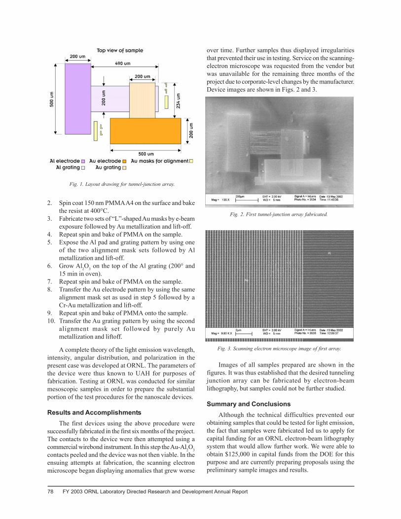
Fabrication by electron-beam lithography was usedin this project in order to obtain the nanometer-scalelinewidths required. The fabrication was carried out via asubcontract with Dr. Greg Norden of the University ofAlabama in Huntsville (UAH). The procedure used wasto first layout the design (Fig. 1) and then carry out thefollowing lithography process:1. Sputter 500-nm SiO2 on silicon wafer for insulation
purposes.
78 FY 2003 ORNL Laboratory Directed Research and Development Annual Report
2. Spin coat 150 nm PMMA A4 on the surface and bakethe resist at 400°C.
3. Fabricate two sets of “L”-shaped Au masks by e-beamexposure followed by Au metallization and lift-off.
4. Repeat spin and bake of PMMA on the sample.5. Expose the Al pad and grating pattern by using one
of the two alignment mask sets followed by Almetallization and lift-off.
6. Grow Al2O3 on the top of the Al grating (200° and15 min in oven).
7. Repeat spin and bake of PMMA on the sample.8. Transfer the Au electrode pattern by using the same
alignment mask set as used in step 5 followed by aCr-Au metallization and lift-off.
9. Repeat spin and bake of PMMA onto the sample.10. Transfer the Au grating pattern by using the second
alignment mask set followed by purely Aumetallization and liftoff.
A complete theory of the light emission wavelength,intensity, angular distribution, and polarization in thepresent case was developed at ORNL. The parameters ofthe device were thus known to UAH for purposes offabrication. Testing at ORNL was conducted for similarmesoscopic samples in order to prepare the substantialportion of the test procedures for the nanoscale devices.
Results and AccomplishmentsThe first devices using the above procedure were
successfully fabricated in the first six months of the project.The contacts to the device were then attempted using acommercial wirebond instrument. In this step the Au-Al2O3contacts peeled and the device was not then viable. In theensuing attempts at fabrication, the scanning electronmicroscope began displaying anomalies that grew worse
Fig. 1. Layout drawing for tunnel-junction array.
Fig. 3. Scanning electron microscope image of first array.
Fig. 2. First tunnel-junction array fabricated.
over time. Further samples thus displayed irregularitiesthat prevented their use in testing. Service on the scanning-electron microscope was requested from the vendor butwas unavailable for the remaining three months of theproject due to corporate-level changes by the manufacturer.Device images are shown in Figs. 2 and 3.
Images of all samples prepared are shown in thefigures. It was thus established that the desired tunnelingjunction array can be fabricated by electron-beamlithography, but samples could not be further studied.
Summary and ConclusionsAlthough the technical difficulties prevented our
obtaining samples that could be tested for light emission,the fact that samples were fabricated led us to apply forcapital funding for an ORNL electron-beam lithographysystem that would allow further work. We were able toobtain $125,000 in capital funds from the DOE for thispurpose and are currently preparing proposals using thepreliminary sample images and results.
Materials Science and Engineering: Seed Money 79
Final Report Project Number: 3210-2062
Dynamic Transport in Nanostructures Z. Zhang,1 A. Eguiluz,1,2 S. T. Pantelides,1,3 and K. Varga1
1Condensed Matter Science Division2University of Tennessee, Knoxville
3Vanderbilt University , Nashville
Conventional microelectronics is already confronting the nanoscale, where quantum phenomenaare inevitable. The time is approaching fast when nanoscale devices will have to exploit quantumphenomena instead of avoiding them. The theoretical understanding of the transport in nanoscaledevices is very important. We have developed new approaches to transport problems which are simplerand more efficient than previous methods. Our research focused on two important areas: the developmentof a novel “source and sink” approach to transport and the development and implementation of thetime-dependent density functional theory (TDDFT) for large-scale simulations of the dynamical aspectsof quantum transport. We have implemented a Lagrange interpolants approach into the TDDFT, whichcombines the rapid convergence of spectral methods with the matrix sparsity of the local (real space)representations. This new technique speeds up the calculations by an order of magnitude, facilitatingdirect-time-step integration in TDDFT.
IntroductionIt is now clear that silion-based technologies are
expected to reach insurmountable roadblocks beyond theyear 2020. One of the most promising directions forovercoming the envisioned obstacles lie in the developmentof a robust nanoscale electronic systems, which promisesto open a whole new world of novel devices and sensorswith outstanding capabilities. Indeed, the past decade hasseen considerable progress in producing experimentalprototypes of such devices. Theoretical progress in thisfield is considerably slower, and it has so far been limitedprimarily to DC transport. There is, however, a substantialinterest in time-dependent transport in nanostructures;dynamic conductance, photon-assisted tunneling, ACcharacteristics, nanostructures in time-varyingelectromagnetic fields, electron pump, electron turnstiles,and frequency-dependent localization, are just a fewexamples where time-dependent electron dynamics playsan extremely important role. In the last few decades, theemphasis of first-principles quantum mechanicalcalculations for molecules and solids has been theelectronic structure of the ground state and the explorationof the available unoccupied states (excited states). It isimportant to note that the transport problem is far morecomplicated than the usual ground-state problem or theproblem of excited states of molecules or crystalline solids,which represent closed systems (the Schrödinger equationamounts to solving an eigenvalue problem). The transportproblem has distinctly different boundary conditions,namely links to reservoirs of electrons with a steady-state
current. We have developed two new and novel approachesto solving the time-dependent or dynamic quantumtransport problem. In the first approach we evaluate anapproach to quantum transport by directly building in“sources and sinks” for the current into the ab initioproblem. In the second approach, we combine theSchrödinger and Maxwell equations and explicitlyintegrate them in time.
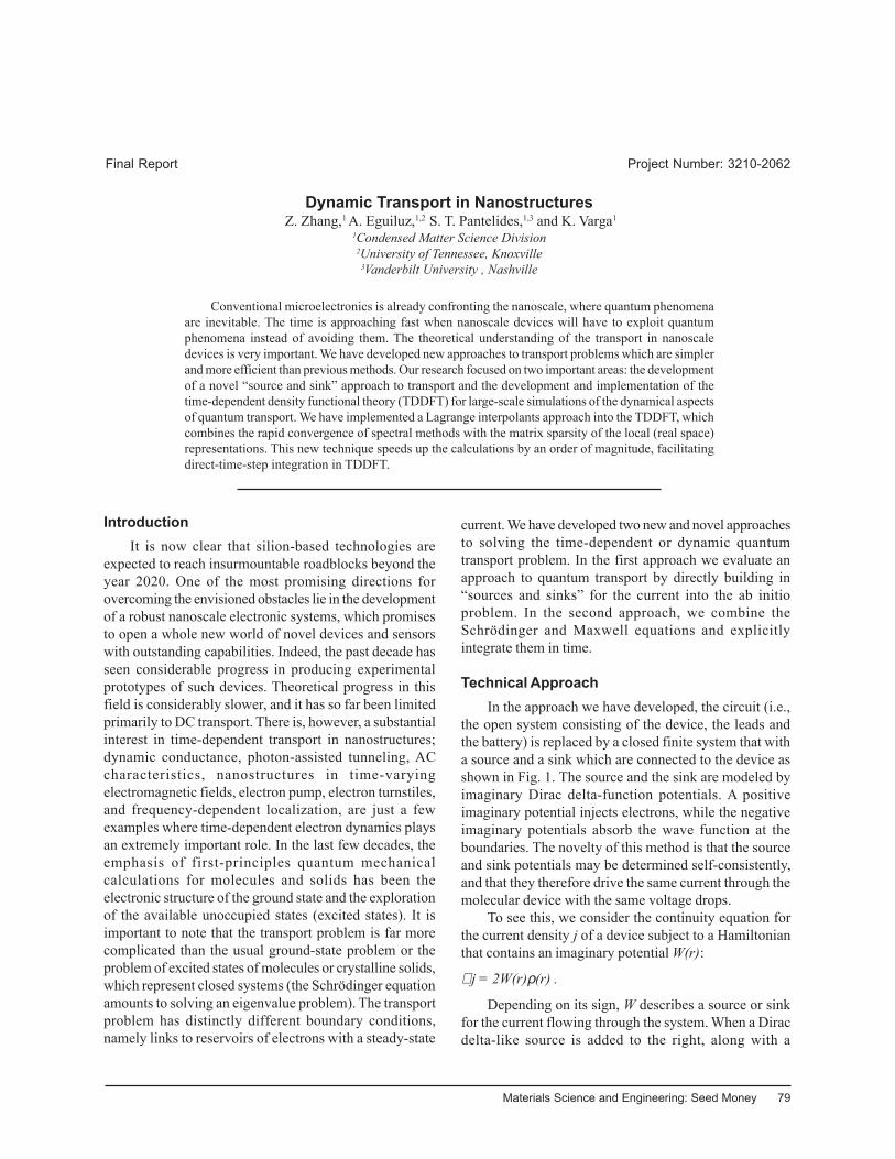
Technical ApproachIn the approach we have developed, the circuit (i.e.,
the open system consisting of the device, the leads andthe battery) is replaced by a closed finite system that witha source and a sink which are connected to the device asshown in Fig. 1. The source and the sink are modeled byimaginary Dirac delta-function potentials. A positiveimaginary potential injects electrons, while the negativeimaginary potentials absorb the wave function at theboundaries. The novelty of this method is that the sourceand sink potentials may be determined self-consistently,and that they therefore drive the same current through themolecular device with the same voltage drops.
To see this, we consider the continuity equation forthe current density j of a device subject to a Hamiltonianthat contains an imaginary potential W(r):
∇ j = 2W(r)ρ(r) .
Depending on its sign, W describes a source or sinkfor the current flowing through the system. When a Diracdelta-like source is added to the right, along with a
80 FY 2003 ORNL Laboratory Directed Research and Development Annual Report
corresponding “sink” term (same potential with theopposite sign) to the right, the corresponding imaginarypotential takes on the form:
)]-(-)-([)(2
)(i RzLzδrρ
IrW δ= .
To impose these injecting and absorbing boundaryconditions, the Schrodinger equation with wavefunction
φ(r) = exp [iG(r)] ϕ(r)
with real functions G(r) and ϕ(r) may be decomposed intoits real and imaginary parts:
)()(])([21 2 rErrGm
H ϕϕ =∇+
and
∇ 2 G(r) ϕ(r) + 2∇ G(r) ∇ ϕ(r) = 2W(r) ρ(r) .
The first equation is a Schrödinger equation with anextra potential term for the real wave function ϕ(r), whilethe second equation is continuity equation of theprobability current j(r) = ∇ G(r) ρ(r),
∇ j(r) = 2W(r) ρ(r) .
The Schrödinger equation and the continuity equationfor ∇ G need to be solved self-consistently.
Results and AccomplishmentsOur initial numerical calculations for simple systems,
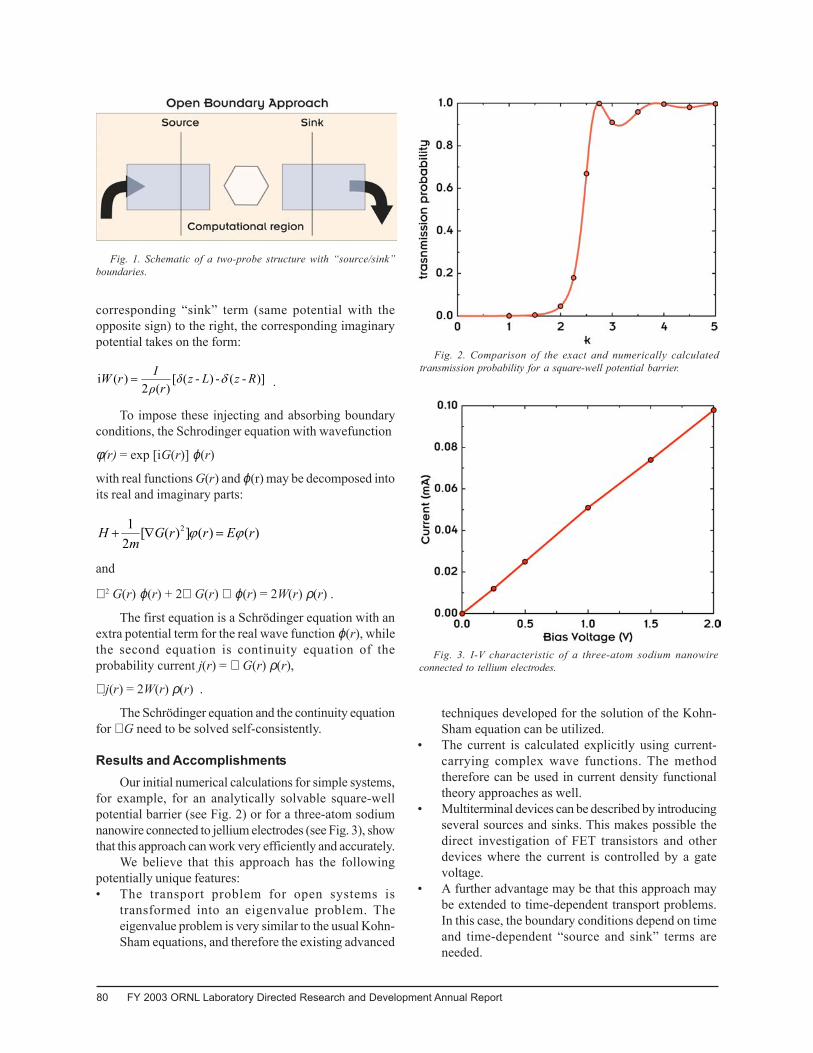
for example, for an analytically solvable square-wellpotential barrier (see Fig. 2) or for a three-atom sodiumnanowire connected to jellium electrodes (see Fig. 3), showthat this approach can work very efficiently and accurately.
We believe that this approach has the followingpotentially unique features:• The transport problem for open systems is
transformed into an eigenvalue problem. Theeigenvalue problem is very similar to the usual Kohn-Sham equations, and therefore the existing advanced
techniques developed for the solution of the Kohn-Sham equation can be utilized.
• The current is calculated explicitly using current-carrying complex wave functions. The methodtherefore can be used in current density functionaltheory approaches as well.
• Multiterminal devices can be described by introducingseveral sources and sinks. This makes possible thedirect investigation of FET transistors and otherdevices where the current is controlled by a gatevoltage.
• A further advantage may be that this approach maybe extended to time-dependent transport problems.In this case, the boundary conditions depend on timeand time-dependent “source and sink” terms areneeded.
Fig. 1. Schematic of a two-probe structure with “source/sink”boundaries.
Fig. 3. I-V characteristic of a three-atom sodium nanowireconnected to tellium electrodes.
Fig. 2. Comparison of the exact and numerically calculatedtransmission probability for a square-well potential barrier.
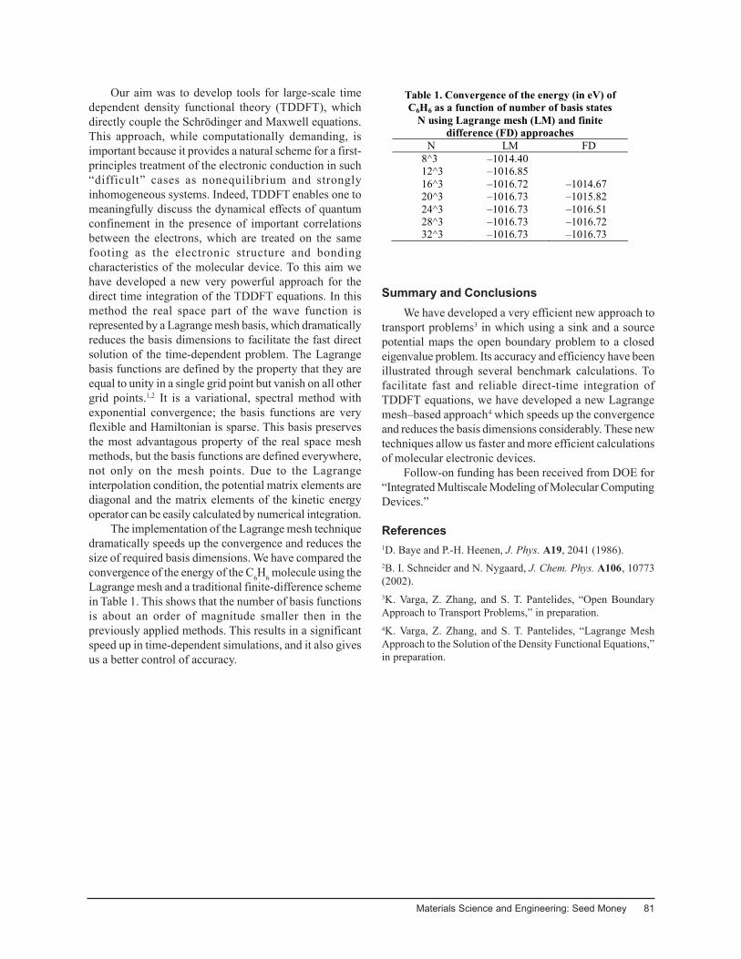
Materials Science and Engineering: Seed Money 81
Our aim was to develop tools for large-scale timedependent density functional theory (TDDFT), whichdirectly couple the Schrödinger and Maxwell equations.This approach, while computationally demanding, isimportant because it provides a natural scheme for a first-principles treatment of the electronic conduction in such“difficult” cases as nonequilibrium and stronglyinhomogeneous systems. Indeed, TDDFT enables one tomeaningfully discuss the dynamical effects of quantumconfinement in the presence of important correlationsbetween the electrons, which are treated on the samefooting as the electronic structure and bondingcharacteristics of the molecular device. To this aim wehave developed a new very powerful approach for thedirect time integration of the TDDFT equations. In thismethod the real space part of the wave function isrepresented by a Lagrange mesh basis, which dramaticallyreduces the basis dimensions to facilitate the fast directsolution of the time-dependent problem. The Lagrangebasis functions are defined by the property that they areequal to unity in a single grid point but vanish on all othergrid points.1,2 It is a variational, spectral method withexponential convergence; the basis functions are veryflexible and Hamiltonian is sparse. This basis preservesthe most advantagous property of the real space meshmethods, but the basis functions are defined everywhere,not only on the mesh points. Due to the Lagrangeinterpolation condition, the potential matrix elements arediagonal and the matrix elements of the kinetic energyoperator can be easily calculated by numerical integration.
The implementation of the Lagrange mesh techniquedramatically speeds up the convergence and reduces thesize of required basis dimensions. We have compared theconvergence of the energy of the C6H6 molecule using theLagrange mesh and a traditional finite-difference schemein Table 1. This shows that the number of basis functionsis about an order of magnitude smaller then in thepreviously applied methods. This results in a significantspeed up in time-dependent simulations, and it also givesus a better control of accuracy.
Summary and ConclusionsWe have developed a very efficient new approach to
transport problems3 in which using a sink and a sourcepotential maps the open boundary problem to a closedeigenvalue problem. Its accuracy and efficiency have beenillustrated through several benchmark calculations. Tofacilitate fast and reliable direct-time integration ofTDDFT equations, we have developed a new Lagrangemesh–based approach4 which speeds up the convergenceand reduces the basis dimensions considerably. These newtechniques allow us faster and more efficient calculationsof molecular electronic devices.
Follow-on funding has been received from DOE for“Integrated Multiscale Modeling of Molecular ComputingDevices.”
References1D. Baye and P.-H. Heenen, J. Phys. A19, 2041 (1986).2B. I. Schneider and N. Nygaard, J. Chem. Phys. A106, 10773(2002).3K. Varga, Z. Zhang, and S. T. Pantelides, “Open BoundaryApproach to Transport Problems,” in preparation.4K. Varga, Z. Zhang, and S. T. Pantelides, “Lagrange MeshApproach to the Solution of the Density Functional Equations,”in preparation.
Table 1. Convergence of the energy (in eV) of C6H6 as a function of number of basis states
N using Lagrange mesh (LM) and finite difference (FD) approaches
N LM FD 8^3 –1014.40 12^3 –1016.85 16^3 –1016.72 –1014.67 20^3 –1016.73 –1015.82 24^3 –1016.73 –1016.51 28^3 –1016.73 –1016.72 32^3 –1016.73 –1016.73
82 FY 2003 ORNL Laboratory Directed Research and Development Annual Report
IntroductionIn the past several years, microelectromechanical
systems (MEMS) have evolved rapidly from an academiccuriosity into a relatively new technology of considerablecommercial and military interest. A crucial element ofMEMS technology is the development of suitablemicroactuators. Thin-film/thick-film magnetostrictivematerials have been recognized recently as a promisingmaterial for making MEMS microsensors andmicroactuators,1–5 due to the low actuating voltage, highactuating force, and fast response. Microactuator devicesutilizing magnetostriction as the actuation mechanism havebeen designed and demonstrated, including micropumps,3–
6 linear ultrasonic motor,3 small flying machine,7 etc.Terfenol-D, based on a ternary Laves phase system
with composition of stoichiometric (TbxDy1–x)Fe2, is thepreferred magnetostrictive material, with strains about0.2% in a field of 10,000 Οe at room temperature.8 Oneimportant issue related to MEMS application ofmagnetostrictive materials is to increase themagnetostriction at low magnetic field and to lower thesaturation field. Recent studies indicated that stabilizationof the amorphous state in (Tb,Dy)Fe2 via alloying additions(such as boron) and rapid cooling could significantlyreduce the saturation field.9–11
Even though amorphization has been found to reducethe saturation field of (Tb,Dy)Fe2 significantly, it has anadverse effect in decreasing the maximum magnetostrictivestrain. What is really desirable for microsystem applicationis to increase the magnetostrictive strain coefficient andmaximum magnetostrictive strain while maintaining thelow saturation field through some innovative approach.In this project, nanocrystalline magnetostrictive materials
Final Report Project Number: 3210-2067
Nanocrystalline Giant Magnetostrictive Materials for Microactuator ApplicationsC. T. Liu,1 J. A. Horton,1 C. L. Fu,1 E. P. George,1 and J. H. Zhu2
1Metals and Ceramics Division2Tennessee Technological University
This project focused on the development of nanocrystalline giant magnetostrictive (GMS) materialsfor next-generation microactuators which will exhibit large-displacement, high-actuating force/energydensity, low-actuating and saturation magnetic fields, rapid response, and compatibility with Simicrofabrication. The project demonstrated that the amorphous state in the (Tb,Dy)Fe2–based systemcould be stabilized by combining alloy design and melt spinning. Initial work showed that by controllingthe annealing condition (i.e., temperature), the crystallization process could be controlled andnanocrystalline GMS materials could be synthesized. It was further indicated that the nanocrystallineGMS materials exhibited higher magnetostriction and/or magnetostrictive strain coefficient, incomparison to both amorphous and fully crystalline GMS materials.
based on (Tb,Dy)Fe2 are proposed to achieve the desiredperformance for MEMS applications.
Technical ApproachTo achieve the desirable performance for the
microactuators, it is proposed to form alignednanocrystalline (Tb,Dy)Fe2 with a size of 1–10 nm in anamorphous matrix by crystallizing amorphous (Tb,Dy)Fe2alloys in controlled magnetic fields. The rationale for suchan approach is as follows: the amorphous matrix and thenanoscale crystalline phase will reduce the magnetoelasticanisotropy of the material, thus retaining the low saturationmagnetic field of the amorphous alloy; under the influenceof magnetic field during crystallization and cooling, thenanocrystalline phase will align themselves in such a waythat the magnetostrictive strain will be maximized, up toor even surpassing the limit of the single-crystal material(0.2%); the reduction of grain size to nanoscale range willimprove magnetic softness of the alloys; for example,coercivity and hysteresis will decrease dramatically.
Since the magnetostrictive properties correlate withthe crystal size, it is important to develop scientific basesto control the grain size of these materials. One veryattractive way to control the grain size of the crystallinematerials is to first stabilize the amorphous state of thematerial, followed by controlled crystallization to get thedesirable nanoscale grain size via thermal treatments. Thisapproach requires a fast cooling rate or enhanced glassformability to obtain a supercooled liquid state.
Recent studies indicate that three metallurgical factorsstrongly affect the glass forming ability of bulk amorphousalloys:12–14
1. multicomponent systems consisting of more than threeelements;
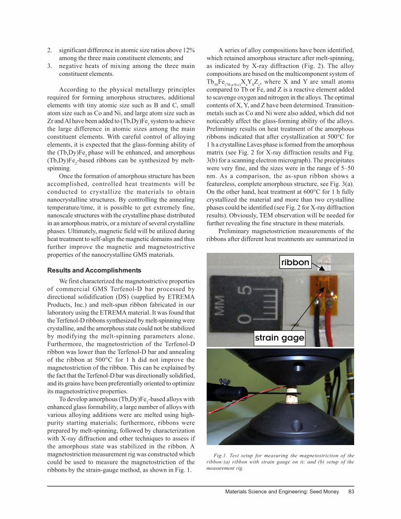
Materials Science and Engineering: Seed Money 83
2. significant difference in atomic size ratios above 12%among the three main constituent elements; and
3. negative heats of mixing among the three mainconstituent elements.
According to the physical metallurgy principlesrequired for forming amorphous structures, additionalelements with tiny atomic size such as B and C, smallatom size such as Co and Ni, and large atom size such asZr and Al have been added to (Tb,Dy)Fe2 system to achievethe large difference in atomic sizes among the mainconstituent elements. With careful control of alloyingelements, it is expected that the glass-forming ability ofthe (Tb,Dy)Fe2 phase will be enhanced, and amorphous(Tb,Dy)Fe2-based ribbons can be synthesized by melt-spinning.
Once the formation of amorphous structure has beenaccomplished, controlled heat treatments will beconducted to crystallize the materials to obtainnanocrystalline structures. By controlling the annealingtemperature/time, it is possible to get extremely fine,nanoscale structures with the crystalline phase distributedin an amorphous matrix, or a mixture of several crystallinephases. Ultimately, magnetic field will be utilized duringheat treatment to self-align the magnetic domains and thusfurther improve the magnetic and magnetostrictiveproperties of the nanocrystalline GMS materials.
Results and AccomplishmentsWe first characterized the magnetostrictive properties
of commercial GMS Terfenol-D bar processed bydirectional solidification (DS) (supplied by ETREMAProducts, Inc.) and melt-spun ribbon fabricated in ourlaboratory using the ETREMA material. It was found thatthe Terfenol-D ribbons synthesized by melt-spinning werecrystalline, and the amorphous state could not be stabilizedby modifying the melt-spinning parameters alone.Furthermore, the magnetostriction of the Terfenol-Dribbon was lower than the Terfenol-D bar and annealingof the ribbon at 500°C for 1 h did not improve themagnetostriction of the ribbon. This can be explained bythe fact that the Terfenol-D bar was directionally solidified,and its grains have been preferentially oriented to optimizeits magnetostrictive properties.
To develop amorphous (Tb,Dy)Fe2-based alloys withenhanced glass formability, a large number of alloys withvarious alloying additions were arc melted using high-purity starting materials; furthermore, ribbons wereprepared by melt-spinning, followed by characterizationwith X-ray diffraction and other techniques to assess ifthe amorphous state was stabilized in the ribbon. Amagnetostriction measurement rig was constructed whichcould be used to measure the magnetostriction of theribbons by the strain-gauge method, as shown in Fig. 1.
A series of alloy compositions have been identified,which retained amorphous structure after melt-spinning,as indicated by X-ray diffraction (Fig. 2). The alloycompositions are based on the multicomponent system ofTb30Fe(70-a-b-c)XaYbZc, where X and Y are small atomscompared to Tb or Fe, and Z is a reactive element addedto scavenge oxygen and nitrogen in the alloys. The optimalcontents of X, Y, and Z have been determined. Transition-metals such as Co and Ni were also added, which did notnoticeably affect the glass-forming ability of the alloys.Preliminary results on heat treatment of the amorphousribbons indicated that after crystallization at 500°C for1 h a crystalline Laves phase is formed from the amorphousmatrix (see Fig. 2 for X-ray diffraction results and Fig.3(b) for a scanning electron micrograph). The precipitateswere very fine, and the sizes were in the range of 5–50nm. As a comparison, the as-spun ribbon shows afeatureless, complete amorphous structure, see Fig. 3(a).On the other hand, heat treatment at 600°C for 1 h fullycrystallized the material and more than two crystallinephases could be identified (see Fig. 2 for X-ray diffractionresults). Obviously, TEM observation will be needed forfurther revealing the fine structure in these materials.
Preliminary magnetostriction measurements of theribbons after different heat treatments are summarized in
Fig.1. Test setup for measuring the magnetostriction of theribbon:(a) ribbon with strain gauge on it; and (b) setup of themeasurement rig.
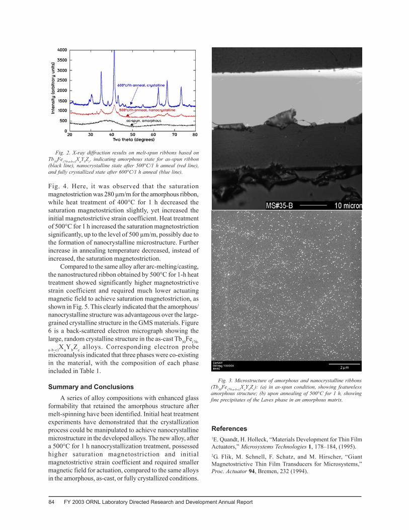
84 FY 2003 ORNL Laboratory Directed Research and Development Annual Report
Fig. 4. Here, it was observed that the saturationmagnetostriction was 280 µm/m for the amorphous ribbon,while heat treatment of 400°C for 1 h decreased thesaturation magnetostriction slightly, yet increased theinitial magnetostrictive strain coefficient. Heat treatmentof 500°C for 1 h increased the saturation magnetostrictionsignificantly, up to the level of 500 µm/m, possibly due tothe formation of nanocrystalline microstructure. Furtherincrease in annealing temperature decreased, instead ofincreased, the saturation magnetostriction.
Compared to the same alloy after arc-melting/casting,the nanostructured ribbon obtained by 500°C for 1-h heattreatment showed significantly higher magnetostrictivestrain coefficient and required much lower actuatingmagnetic field to achieve saturation magnetostriction, asshown in Fig. 5. This clearly indicated that the amorphous/nanocrystalline structure was advantageous over the large-grained crystalline structure in the GMS materials. Figure6 is a back-scattered electron micrograph showing thelarge, random crystalline structure in the as-cast Tb30Fe(70-
a-b-c)XaYbZc alloys. Corresponding electron probemicroanalysis indicated that three phases were co-existingin the material, with the composition of each phaseincluded in Table 1.
Summary and ConclusionsA series of alloy compositions with enhanced glass
formability that retained the amorphous structure aftermelt-spinning have been identified. Initial heat treatmentexperiments have demonstrated that the crystallizationprocess could be manipulated to achieve nanocrystallinemicrostructure in the developed alloys. The new alloy, aftera 500°C for 1 h nanocrystallization treatment, possessedhigher saturation magnetostriction and initialmagnetostrictive strain coefficient and required smallermagnetic field for actuation, compared to the same alloysin the amorphous, as-cast, or fully crystallized conditions.
References1E. Quandt, H. Holleck, “Materials Development for Thin FilmActuators,” Microsystems Technologies 1, 178–184, (1995).2G. Flik, M. Schnell, F. Schatz, and M. Hirscher, “GiantMagnetostrictive Thin Film Transducers for Microsystems,”Proc. Actuator 94, Bremen, 232 (1994).
Fig. 2. X-ray diffraction results on melt-spun ribbons based onTb30Fe(70-a-b-c)XaYbZc, indicating amorphous state for as-spun ribbon(black line), nanocrystalline state after 500°C/1 h anneal (red line),and fully crystallized state after 600°C/1 h anneal (blue line).
Fig. 3. Microstructure of amorphous and nanocrystalline ribbons(Tb30Fe(70-a-b-c)XaYbZc): (a) in as-spun condition, showing featurelessamorphous structure; (b) upon annealing of 500°C for 1 h, showingfine precipitates of the Laves phase in an amorphous matrix.
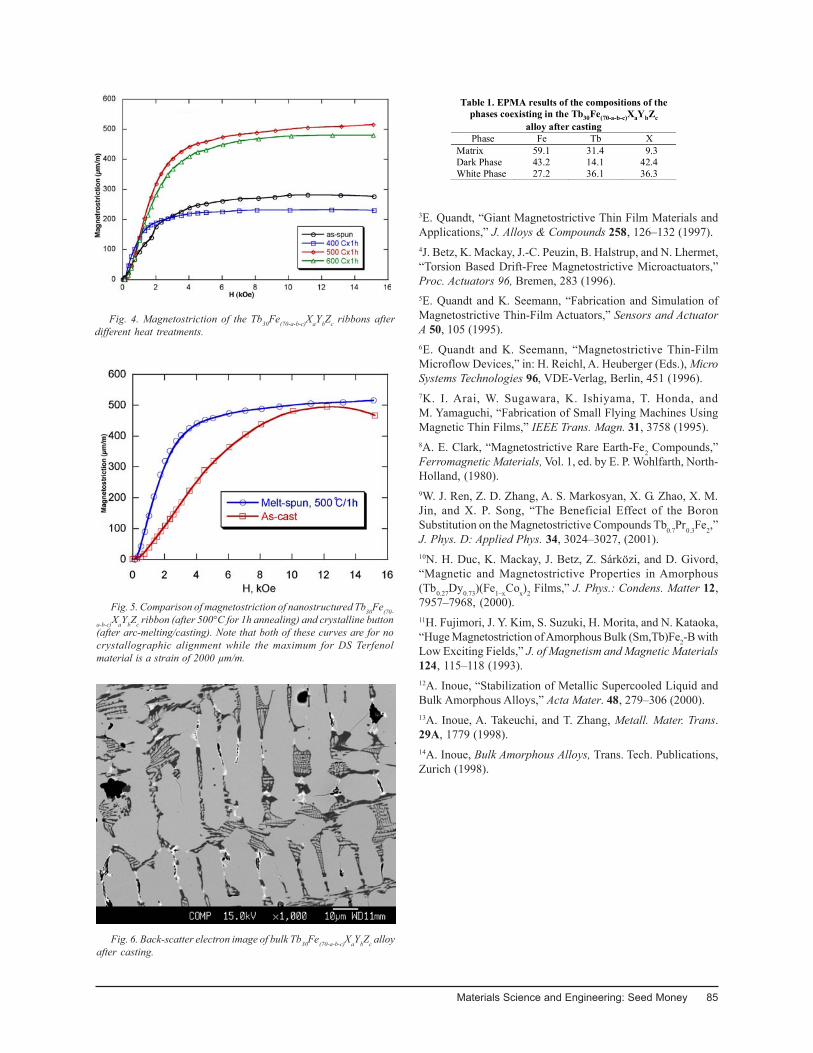
Materials Science and Engineering: Seed Money 85
3E. Quandt, “Giant Magnetostrictive Thin Film Materials andApplications,” J. Alloys & Compounds 258, 126–132 (1997).4J. Betz, K. Mackay, J.-C. Peuzin, B. Halstrup, and N. Lhermet,“Torsion Based Drift-Free Magnetostrictive Microactuators,”Proc. Actuators 96, Bremen, 283 (1996).5E. Quandt and K. Seemann, “Fabrication and Simulation ofMagnetostrictive Thin-Film Actuators,” Sensors and ActuatorA 50, 105 (1995).6E. Quandt and K. Seemann, “Magnetostrictive Thin-FilmMicroflow Devices,” in: H. Reichl, A. Heuberger (Eds.), MicroSystems Technologies 96, VDE-Verlag, Berlin, 451 (1996).7K. I. Arai, W. Sugawara, K. Ishiyama, T. Honda, andM. Yamaguchi, “Fabrication of Small Flying Machines UsingMagnetic Thin Films,” IEEE Trans. Magn. 31, 3758 (1995).8A. E. Clark, “Magnetostrictive Rare Earth-Fe2 Compounds,”Ferromagnetic Materials, Vol. 1, ed. by E. P. Wohlfarth, North-Holland, (1980).9W. J. Ren, Z. D. Zhang, A. S. Markosyan, X. G. Zhao, X. M.Jin, and X. P. Song, “The Beneficial Effect of the BoronSubstitution on the Magnetostrictive Compounds Tb0.7Pr0.3Fe2,”J. Phys. D: Applied Phys. 34, 3024–3027, (2001).10N. H. Duc, K. Mackay, J. Betz, Z. Sárközi, and D. Givord,“Magnetic and Magnetostrictive Properties in Amorphous(Tb0.27Dy0.73)(Fe1–xCox)2 Films,” J. Phys.: Condens. Matter 12,7957–7968, (2000).11H. Fujimori, J. Y. Kim, S. Suzuki, H. Morita, and N. Kataoka,“Huge Magnetostriction of Amorphous Bulk (Sm,Tb)Fe2-B withLow Exciting Fields,” J. of Magnetism and Magnetic Materials124, 115–118 (1993).12A. Inoue, “Stabilization of Metallic Supercooled Liquid andBulk Amorphous Alloys,” Acta Mater. 48, 279–306 (2000).13A. Inoue, A. Takeuchi, and T. Zhang, Metall. Mater. Trans.29A, 1779 (1998).14A. Inoue, Bulk Amorphous Alloys, Trans. Tech. Publications,Zurich (1998).
Fig. 4. Magnetostriction of the Tb30Fe(70-a-b-c)XaYbZc ribbons afterdifferent heat treatments.
Fig. 5. Comparison of magnetostriction of nanostructured Tb30Fe(70-
a-b-c)XaYbZc ribbon (after 500°C for 1h annealing) and crystalline button(after arc-melting/casting). Note that both of these curves are for nocrystallographic alignment while the maximum for DS Terfenolmaterial is a strain of 2000 µm/m.
Fig. 6. Back-scatter electron image of bulk Tb30Fe(70-a-b-c)XaYbZc alloyafter casting.
Table 1. EPMA results of the compositions of the phases coexisting in the Tb30Fe(70-a-b-c)XaYbZc
alloy after casting Phase Fe Tb X
Matrix 59.1 31.4 9.3 Dark Phase 43.2 14.1 42.4 White Phase 27.2 36.1 36.3
86 FY 2003 ORNL Laboratory Directed Research and Development Annual Report
Final Report Project Number: 3210-2070
Probing Charge Transport in Oriented Conducting Polymer Nanostructures:Toward Integrated Molecular Optoelectronics
M. D. BarnesChemical Sciences Division
This project focused on measurement and modeling of charge transport and optically gatedconductivity in oriented polymer nanorods. This idea was based on newly discovered techniques forproducing oriented semiconducting polymer nanoparticles with structural and photophysical propertiesthat are quite different from bulk material. The specific goals of this project were to probe chargetransport behavior of isolated polymer nanoparticles and electronic coupling between polymer chainsand molecular wire/logic structures as first steps toward enabling an optical interface to molecular-level electronic circuitry, and use of polymeric materials in the newly emerging field of nanoscaleoptoelectronics.
IntroductionNanophotonics—or molecular-scale optoelec-
tronics—is a rapidly emerging area of research thatcombines nanoscale optical elements (e.g., single-molecules, or quantum dots) and molecular-scaleelectronics. Such “photonic elements” could ultimatelyprovide a route for connecting the macroscopic andnanoscopic worlds through absorption or emission ofphotons coupled with electron (or hole) motion to or from,say, a molecular wire or gate structure. Here the materialschallenge in design and fabrication of such elements isdaunting: For practical applications, one needs nanoscalecomponents with well-defined transition energies anddipole moment orientation for spatially selectiveaddressability, as well as robust photostability and facilecharge transport properties. Because of the inherent sizescalability, responsiveness to optical excitation, and longhistory in mesoscale photonics, semiconducting polymersmake attractive candidates for nanoscale optoelectronics.However, in conventional thin film formats, these speciesare formed with random in-plane orientation with a broaddistribution of chain morphologies and tend to be quitefragile with respect to repeated optical excitation.
The inherent size scalability and large parameter spaceassociated with structural and electronic properties ofsemiconducting polymers1 make them interestingcandidates for the purpose of interfacing andinterconnecting nanoscale logic units. The work of JamesTour,2 for example, has focused on synthetic techniquesto fabricate molecular “wires” from conducting polymerswith specifically designed branch architectures and end-group functionalities. However, in addition to difficultiesin controlling the orientation and chain alignment ofsemiconducting polymers such as polyphenylene vinylene
(PPV) derivatives, these species tend to be quite fragilewith respect to repeated electronic excitation. Furthermore,most strategies for organizing conducting chain segmentsare based on molecular self-assembly which restricts therange of device geometries and position of the desiredspecies. While gel-processing3 or templating techniques4
have been used to produce axially aligned conductingpolymers, these strategies lack the molecular-leveladdressability and connectivity needed for multiplexedoptoelectronic applications.
Our research program was designed to exploit recentexperimental results in our laboratory that havedemonstrated the ability to “print” single molecules of aconducting polymer with dramatically altered structuraland photophysical properties relative to conventional thin-film preparations.5,6 We observed luminescencecharacteristics strikingly similar to those recently observedfor cadmium-selenide quantum rods7 suggesting a highlyordered chain configuration with exciton delocalizationwithin the particle. In addition to linear polarization inemission and modification of spectral characteristics, wefound uniform particle orientation and a two-order-ofmagnitude enhancement in photostability relative to similarmolecules deposited (from the same solution) by spin-casting. This modification of structural and photophysicalproperties derives in part from the effect of three-dimensional confinement by the liquid droplet of solutionas it evaporates en route to the substrate.8 As a result, thisis a highly general method of preparing different kinds ofnanostructured polymer systems for molecular scaleoptoelectronics with tailorable properties (absorption/emission frequencies, chain morphologies etc.). We findthat many important luminescence characteristics arepreserved—and in some cases enhanced further—bydoping the polymer solution with other materials.
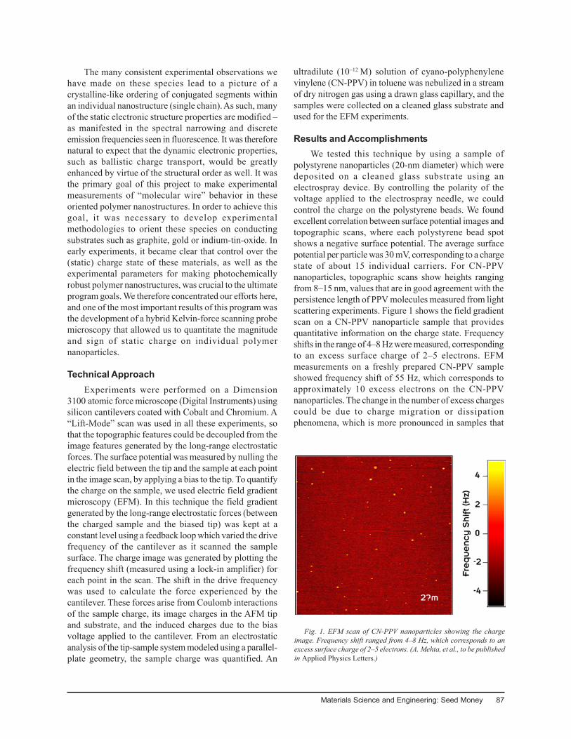
Materials Science and Engineering: Seed Money 87
The many consistent experimental observations wehave made on these species lead to a picture of acrystalline-like ordering of conjugated segments withinan individual nanostructure (single chain). As such, manyof the static electronic structure properties are modified –as manifested in the spectral narrowing and discreteemission frequencies seen in fluorescence. It was thereforenatural to expect that the dynamic electronic properties,such as ballistic charge transport, would be greatlyenhanced by virtue of the structural order as well. It wasthe primary goal of this project to make experimentalmeasurements of “molecular wire” behavior in theseoriented polymer nanostructures. In order to achieve thisgoal, it was necessary to develop experimentalmethodologies to orient these species on conductingsubstrates such as graphite, gold or indium-tin-oxide. Inearly experiments, it became clear that control over the(static) charge state of these materials, as well as theexperimental parameters for making photochemicallyrobust polymer nanostructures, was crucial to the ultimateprogram goals. We therefore concentrated our efforts here,and one of the most important results of this program wasthe development of a hybrid Kelvin-force scanning probemicroscopy that allowed us to quantitate the magnitudeand sign of static charge on individual polymernanoparticles.
Technical ApproachExperiments were performed on a Dimension
3100 atomic force microscope (Digital Instruments) usingsilicon cantilevers coated with Cobalt and Chromium. A“Lift-Mode” scan was used in all these experiments, sothat the topographic features could be decoupled from theimage features generated by the long-range electrostaticforces. The surface potential was measured by nulling theelectric field between the tip and the sample at each pointin the image scan, by applying a bias to the tip. To quantifythe charge on the sample, we used electric field gradientmicroscopy (EFM). In this technique the field gradientgenerated by the long-range electrostatic forces (betweenthe charged sample and the biased tip) was kept at aconstant level using a feedback loop which varied the drivefrequency of the cantilever as it scanned the samplesurface. The charge image was generated by plotting thefrequency shift (measured using a lock-in amplifier) foreach point in the scan. The shift in the drive frequencywas used to calculate the force experienced by thecantilever. These forces arise from Coulomb interactionsof the sample charge, its image charges in the AFM tipand substrate, and the induced charges due to the biasvoltage applied to the cantilever. From an electrostaticanalysis of the tip-sample system modeled using a parallel-plate geometry, the sample charge was quantified. An
ultradilute (10–12 M) solution of cyano-polyphenylenevinylene (CN-PPV) in toluene was nebulized in a streamof dry nitrogen gas using a drawn glass capillary, and thesamples were collected on a cleaned glass substrate andused for the EFM experiments.
Results and AccomplishmentsWe tested this technique by using a sample of
polystyrene nanoparticles (20-nm diameter) which weredeposited on a cleaned glass substrate using anelectrospray device. By controlling the polarity of thevoltage applied to the electrospray needle, we couldcontrol the charge on the polystyrene beads. We foundexcellent correlation between surface potential images andtopographic scans, where each polystyrene bead spotshows a negative surface potential. The average surfacepotential per particle was 30 mV, corresponding to a chargestate of about 15 individual carriers. For CN-PPVnanoparticles, topographic scans show heights rangingfrom 8–15 nm, values that are in good agreement with thepersistence length of PPV molecules measured from lightscattering experiments. Figure 1 shows the field gradientscan on a CN-PPV nanoparticle sample that providesquantitative information on the charge state. Frequencyshifts in the range of 4–8 Hz were measured, correspondingto an excess surface charge of 2–5 electrons. EFMmeasurements on a freshly prepared CN-PPV sampleshowed frequency shift of 55 Hz, which corresponds toapproximately 10 excess electrons on the CN-PPVnanoparticles. The change in the number of excess chargescould be due to charge migration or dissipationphenomena, which is more pronounced in samples that
Fig. 1. EFM scan of CN-PPV nanoparticles showing the chargeimage. Frequency shift ranged from 4–8 Hz, which corresponds to anexcess surface charge of 2–5 electrons. (A. Mehta, et al., to be publishedin Applied Physics Letters.)
88 FY 2003 ORNL Laboratory Directed Research and Development Annual Report
are exposed to ambient conditions for long periods of time.These results confirm that the CN-PPV nanoparticlesproduced by the nebulization technique are negativelycharged with an excess charge ranging from two to tenelectrons. This suggests that these particles could beattached to a conducting surface with an appropriatecationic coating. Using a metal-coated biased cantilever,individual nanoparticles could be addressed to study theI-V characteristics of these nanostructures.
Summary and ConclusionsOur results provided definitive proof that the
semiconducting nanoparticles produced by thenebulization technique are negatively charged with anexcess charge ranging from two to ten electrons.9 Thisvalue is in good agreement with values estimated fromRayleigh stability limits for a particle of this size. Theseresults suggests that these particles could be attached to aconducting surface with an appropriate cationic coating.Using a metal-coated biased cantilever, individualnanoparticles could be addressed to study the I-Vcharacteristics of these nanostructures. Many questionsremain: Are specific charge states (higher or lower)correlated with photochemical properties? How does thechemical potential (electron affinity) depend on chargestate? This question is of particular importance in relationto nanoscale optoelectronic device functionality. Whileour experimental path diverged somewhat from ouroriginal proposal, we have made significant progress inour microscopic understanding of the nature of these highlynovel polymeric species and the results described hereprovide a solid scientific foundation for furtherinvestigation.
References1A. J. Heeger, “Semiconducting and Metallic Polymers: TheFourth Generation of Polymeric Materials,” J. Phys. Chem.B 105, 8475 (2001).2J. M. Tour, “Molecular Electronics: Synthesis and Testing ofComponents,” Acc. Chem. Res. 33, 791 (2000).3T. W. Hagler, K. Pakbaz, and A. J. Heeger, “Polarized-Electroabsorption Spectroscopy of a Soluble Derivative ofPoly(P-Phenylenevinylene) Oriented by Gel Processing InPolyethylene- Polarization Anisotropy, the Off-Axis DipoleMoment, and Excited State Delocalization,” Phys Rev. B 49,10968 (1994).4T. Q. Nguyen, J. J. Wu, V. Doan, B. J. Schwartz, and S. Tolbert,“Control Of Energy Transfer In Oriented Polymer-MesoporousSilica Composites,” Science 288, 652 (2000).5P. Kumar, A. Mehta, M. Dadmun, J. Zheng, L. Peyser, R. M.Dickson, T. Thundat, B. G. Sumpter, and M. D. Barnes,“Observation of narrow-bandwith spontaneous luminescencefrom oriented conjugated polymer nanostructures,” J. Phys.Chem. B 107, 6252–6257 (2003). [Letter to the Editor]6A. Mehta, P. Kumar, M. Dadmun, J. Zheng, R. M. Dickson,T. Thundat, B. G. Sumpter, and M. D. Barnes, “Orientedcylindrical nanostructures of a semiconducting polymer:Polarization evidence for highly ordered individualmacromolecular structures,” Nanoletters 3(5), 603–607 (2003).7J. Hu, L-S. Li, W. Yang, L. Manna, L-W. Wang, and A. P.Alivisatos, “Linearly polarized emission from colloidalsemiconductor quantum rods,” Science 292, 2060 (2001).8M. D. Barnes, B. G. Sumpter, and D. W. Noid, “Polymer-blendmicroparticles: A new approach to nanoscale composites withtunable properties,” Materials Today (invited) 2(3), 25–27(1999).9A. Mehta, P. Kumar, T. Thundat, and M. D. Barnes,“Investigation of static charge states of oriented semiconductingpolymer nanostructures,” to be published in Applied PhysicsLetters.
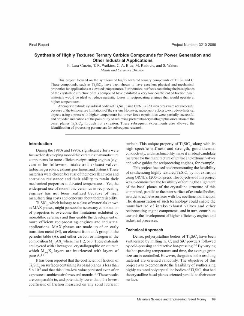
Materials Science and Engineering: Seed Money 89
Final Report Project Number: 3210-2080
Synthesis of Highly Textured Ternary Carbide Compounds for Power Generation andOther Industrial Applications
E. Lara-Curzio, T. R. Watkins, C. A. Blue, M. Radovic, and S. WatersMetals and Ceramics Division
This project focused on the synthesis of highly textured ternary compounds of Ti, Si, and C.These compounds, such as Ti3SiC2, have been shown to have excellent physical and mechanicalproperties for applications at elevated temperatures. Furthermore, surfaces containing the basal planesof the crystalline structure of this compound have exhibited a very low coefficient of friction. Suchmaterials would be ideal to reduce parasitic losses in reciprocating engines that would operate athigher temperatures.
Attempts to extrude cylindrical bodies of Ti3SiC2 using ORNL’s 1200-ton press were not successfulbecause of the temperature limitations of the system. However, subsequent efforts to extrude cylindricalobjects using a press with higher temperature but lower force capabilities were partially successfuland provided indications of the possibility of achieving preferential crystallographic orientation of thebasal planes Ti3SiC2, through hot extrusion. These subsequent experiments also allowed theidentification of processing parameters for subsequent research.
IntroductionDuring the 1980s and 1990s, significant efforts were
focused on developing monolithic ceramics to manufacturecomponents for more efficient reciprocating engines (e.g.,cam roller followers, intake and exhaust valves,turbocharger rotors, exhaust port liners, and pistons). Thesematerials were chosen because of their excellent wear andcorrosion resistance and their ability to retain theirmechanical properties at elevated temperatures.1 Yet, thewidespread use of monolithic ceramics in reciprocatingengines has not been realized because of highmanufacturing costs and concerns about their reliability.
Ti3SiC2, which belongs to a class of materials knownas MAX phases, might possess the necessary combinationof properties to overcome the limitations exhibited bymonolithic ceramics and thus enable the development ofmore efficient reciprocating engines and industrialapplications. MAX phases are made up of an earlytransition metal (M), an element from an A group in theperiodic table (A), and either carbon or nitrogen in thecomposition Mn+1AXn where n is 1, 2, or 3. These materialsare layered with a hexagonal crystallographic structure inwhich Mn+1Xn layers are interleaved with layers ofpure A.2–3
It has been reported that the coefficient of friction ofTi3SiC2 on surfaces containing its basal planes is less than5 × 10–3 and that this ultra-low value persisted even afterexposure to ambient air for several months.4–5 These resultsare comparable to, and potentially lower than, the lowestcoefficient of friction measured on any solid lubricant
surface. This unique property of Ti3SiC2, along with itshigh specific stiffness and strength, good thermalconductivity, and machinability make it an ideal candidatematerial for the manufacture of intake and exhaust valvesand valve guides for reciprocating engines, for example.
This project focused on demonstrating the feasibilityof synthesizing highly textured Ti3SiC2 by hot extrusionusing ORNL’s 1200-ton press. The objective of this projectwas to demonstrate the feasibility of forcing the alignmentof the basal planes of the crystalline structure of thiscompound, parallel to the outer surface of extruded bodies,in order to achieve surfaces with low coefficient of friction.The demonstration of such technology could enable themanufacture of intake/exhaust valves and otherreciprocating engine components, and in turn, contributetowards the development of higher efficiency engines andindustrial processes.
Technical ApproachDense, polycrystalline bodies of Ti3SiC2 have been
synthesized by milling Ti, C, and SiC powders followedby cold-pressing and reactive hot-pressing.2–3 By varyingthe hot-pressing temperature and time, the average grainsize can be controlled. However, the grains in the resultingmaterial are oriented randomly. The objective of thisproject was to demonstrate the feasibility of synthesizinghighly textured polycrystalline bodies of Ti3SiC2 that hadthe crystalline basal planes oriented parallel to their outersurface.
90 FY 2003 ORNL Laboratory Directed Research and Development Annual Report
It has been documented that during extrusion, orduring other processes that involve shearing of viscousfluids, anisometric particles align so that their long axis isparallel to the extrusion direction due to shear developedbetween the extrusion nozzle and the material beingextruded.6 In crystalline materials, slip planes are usuallythe planes with the highest density of atoms. In the case ofhexagonal crystals slip will occur on the basal planes.Therefore, during hot extrusion, when the material candeform plastically, deformation will be easiest along thebasal planes, which will align parallel to the extrusiondirection. For example, pronounced textures have beenachieved through the hot extrusion of superconductingcompounds of YBa2Cu3Ox and Bi2Sr2CaCu2O8+X where thebasal planes became aligned along the direction ofextrusion.7–8
To achieve the objective of this project, a series ofhot extrusion runs were carried out using ORNL’s 1200-tonextrusion press. Starting powders of Ti3SiC2 with particlesize of 1–5 µm were canned under vacuum (>4 × 10⁻⁴
torr) inside tantalum-lined 304 stainless steel ormolybdenum cans, which were subsequently sealed byelectron-beam welding. Extrusion runs were carried outafter the cans had been heated inside a furnace attemperatures between 1100°C and 1300°C for 1 h.Additional attempts to extrude Ti3SiC2 were carried outusing a hot-press with higher temperature capabilities, butlower force capacity. In this case, conical dies weremanufactured with three different extrusion ratios between1:2.6 and 1:4 and an angle of 60° using high-strengthgraphite. The dies were 127 mm in diameter and 171 mmin length. To minimize friction, the die was lined with a50-µm thick layer of Graphoil®. Hot extrusion runs at
temperatures as high as 1700°C were carried out and themicrostructure of the resulting materials was characterizedusing conventional metallographic techniques and X-raydiffraction methods for phase identification.
Results and AccomplishmentsAttempts to extrude Ti3SiC2 at temperatures between
1100°C and 1300°C and with forces as high as 500 tonswere unsuccessful using ORNL’s 1200-ton press. One-half of the cans that were prepared failed to extrude throughdies with diameters of either 12.5 mm or 15.8 mm. Theremaining extrusions had tears or broke in several piecesafter exiting the die and revealed poor consolidation ofthe Ti3SiC2 powders (Fig. 1). These results suggested thatthe temperatures used were not sufficiently high toconsolidate the powders and to allow for creep/plastic flow.Although the furnace used to heat up the cans beforeextrusion can operate in excess of 1300°C, there aren’tmany materials to fabricate cans capable of withstandingtemperatures above 1300°C in air.
The failure to hot-extrude Ti3SiC2 using ORNL’s1200-ton extrusion press prompted the search foralternative strategies to accomplish the objectives of thisproject. Additional hot-extrusions were carried out usinga hydraulic press equipped with a graphite furnace capableof 2000°C in vacuum or inert environment. Extrusionexperiments were carried out in two steps using this system.In the first step powders were densified at 1400°C invacuum under an axial force of 10 kN inside a conicalgraphite mold lined with Graphoil®. This resulted in verydense products. In the second step, the densified bodieswere extruded at temperatures between 1400°C and1700°C and forces as high as 17.5 kN using high-strengthconical graphite dies with extrusion ratios between 1:2.6and 1:4 and an angle of 60° using. The dies were 127 mmin diameter and 171 mm in length. To minimize friction,the die was lined with a 50-µm-thick layer of Graphoil®.Although it was possible to extrude the material (Fig. 2),the amount of extrusion was very small. There wasevidence of reaction between the layer of Graphoil® andTi3SiC2, which resulted in the formation of titaniumcarbide. An X-ray diffraction analysis also revealed thatthe intensity of the peak associated with the basal planeon a surface of the extruded body parallel to the extrusiondirection was 3.5 times larger than the intensity of the peakassociated with this plane on a surface perpendicular tothe extrusion direction (Fig. 3).
While the results from this investigation havedemonstrated the possibility of extruding Ti3SiC2, albeitin a small amount, and the preferential alignment of itscrystalline planes, they also showed the good resistanceof Ti3SiC2 to creep deformation, which should beconsidered a good trait. The ability to hot-extrude Ti3SiC2could be improved by using an alternative lubricant (e.g.,
Fig. 1. Photograph of hot-extruded Ti3SiC2 in a tantalum-lined 304stainless steel can. The extrusion products had tears and broke inseveral pieces.
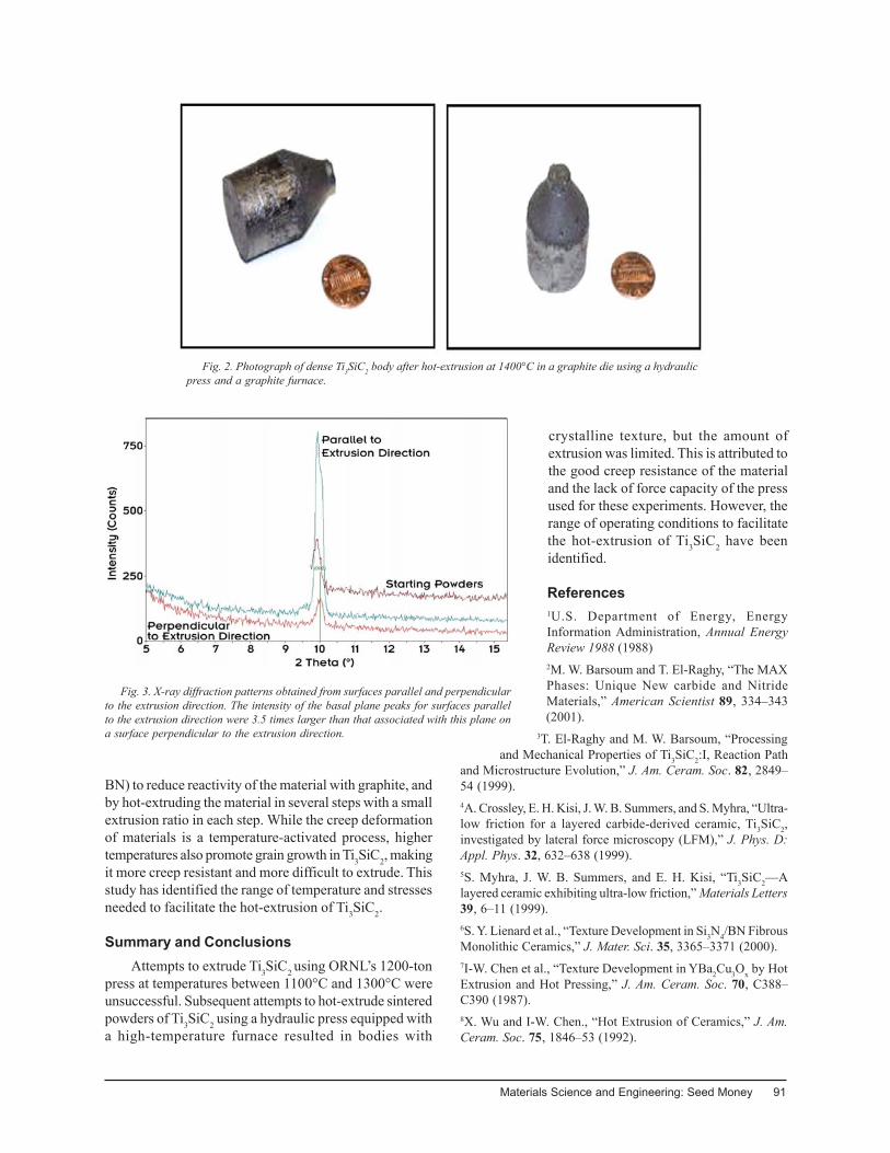
Materials Science and Engineering: Seed Money 91
BN) to reduce reactivity of the material with graphite, andby hot-extruding the material in several steps with a smallextrusion ratio in each step. While the creep deformationof materials is a temperature-activated process, highertemperatures also promote grain growth in Ti3SiC2, makingit more creep resistant and more difficult to extrude. Thisstudy has identified the range of temperature and stressesneeded to facilitate the hot-extrusion of Ti3SiC2.
Summary and ConclusionsAttempts to extrude Ti3SiC2 using ORNL’s 1200-ton
press at temperatures between 1100°C and 1300°C wereunsuccessful. Subsequent attempts to hot-extrude sinteredpowders of Ti3SiC2 using a hydraulic press equipped witha high-temperature furnace resulted in bodies with
Fig. 2. Photograph of dense Ti3SiC2 body after hot-extrusion at 1400°C in a graphite die using a hydraulicpress and a graphite furnace.
crystalline texture, but the amount ofextrusion was limited. This is attributed tothe good creep resistance of the materialand the lack of force capacity of the pressused for these experiments. However, therange of operating conditions to facilitatethe hot-extrusion of Ti3SiC2 have beenidentified.
References1U.S. Department of Energy, EnergyInformation Administration, Annual EnergyReview 1988 (1988)2M. W. Barsoum and T. El-Raghy, “The MAXPhases: Unique New carbide and NitrideMaterials,” American Scientist 89, 334–343(2001).
3T. El-Raghy and M. W. Barsoum, “Processingand Mechanical Properties of Ti3SiC2:I, Reaction Path
and Microstructure Evolution,” J. Am. Ceram. Soc. 82, 2849–54 (1999).4A. Crossley, E. H. Kisi, J. W. B. Summers, and S. Myhra, “Ultra-low friction for a layered carbide-derived ceramic, Ti3SiC2,investigated by lateral force microscopy (LFM),” J. Phys. D:Appl. Phys. 32, 632–638 (1999).5S. Myhra, J. W. B. Summers, and E. H. Kisi, “Ti3SiC2—Alayered ceramic exhibiting ultra-low friction,” Materials Letters39, 6–11 (1999).6S. Y. Lienard et al., “Texture Development in Si3N4/BN FibrousMonolithic Ceramics,” J. Mater. Sci. 35, 3365–3371 (2000).7I-W. Chen et al., “Texture Development in YBa2Cu3Ox by HotExtrusion and Hot Pressing,” J. Am. Ceram. Soc. 70, C388–C390 (1987).8X. Wu and I-W. Chen., “Hot Extrusion of Ceramics,” J. Am.Ceram. Soc. 75, 1846–53 (1992).
Fig. 3. X-ray diffraction patterns obtained from surfaces parallel and perpendicularto the extrusion direction. The intensity of the basal plane peaks for surfaces parallelto the extrusion direction were 3.5 times larger than that associated with this plane ona surface perpendicular to the extrusion direction.
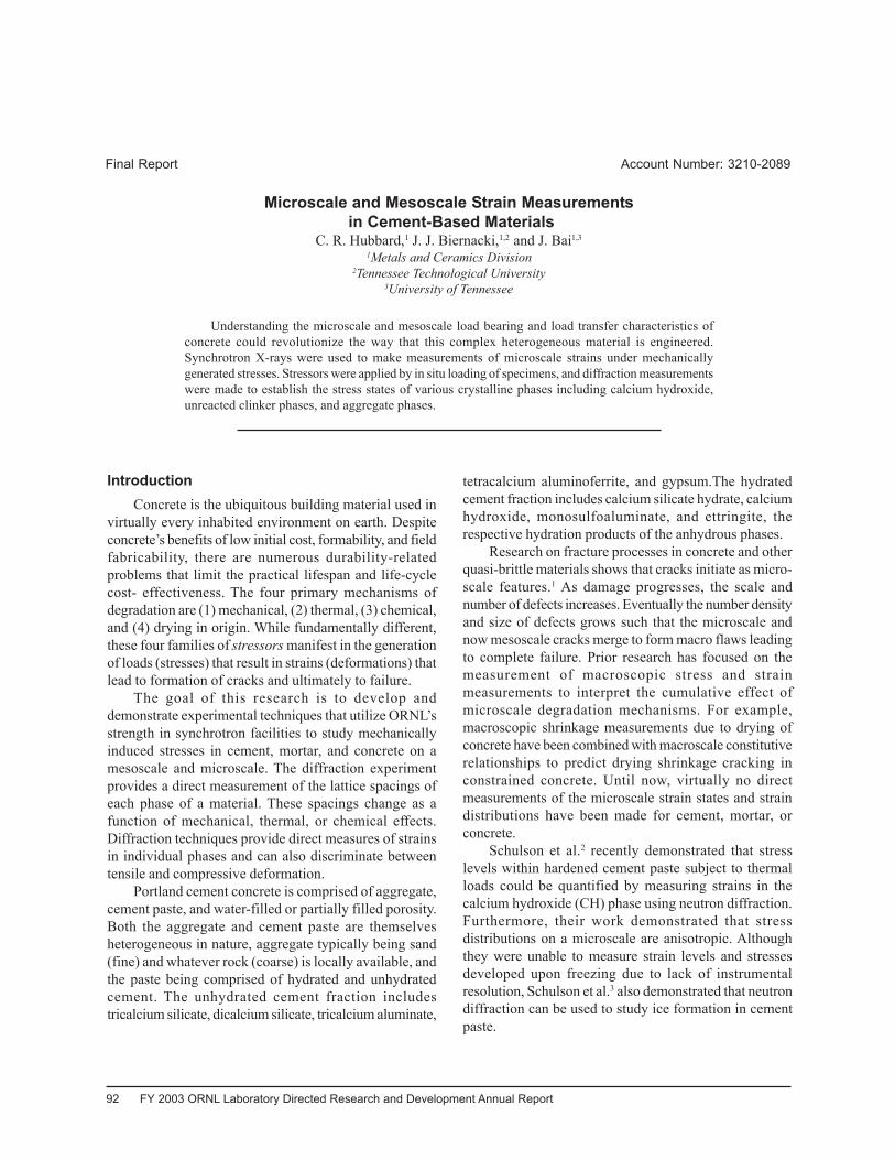
92 FY 2003 ORNL Laboratory Directed Research and Development Annual Report
Final Report Account Number: 3210-2089
Microscale and Mesoscale Strain Measurements in Cement-Based Materials
C. R. Hubbard,1 J. J. Biernacki,1,2 and J. Bai1,3
1Metals and Ceramics Division2Tennessee Technological University
3University of Tennessee
Understanding the microscale and mesoscale load bearing and load transfer characteristics ofconcrete could revolutionize the way that this complex heterogeneous material is engineered.Synchrotron X-rays were used to make measurements of microscale strains under mechanicallygenerated stresses. Stressors were applied by in situ loading of specimens, and diffraction measurementswere made to establish the stress states of various crystalline phases including calcium hydroxide,unreacted clinker phases, and aggregate phases.
IntroductionConcrete is the ubiquitous building material used in
virtually every inhabited environment on earth. Despiteconcrete’s benefits of low initial cost, formability, and fieldfabricability, there are numerous durability-relatedproblems that limit the practical lifespan and life-cyclecost- effectiveness. The four primary mechanisms ofdegradation are (1) mechanical, (2) thermal, (3) chemical,and (4) drying in origin. While fundamentally different,these four families of stressors manifest in the generationof loads (stresses) that result in strains (deformations) thatlead to formation of cracks and ultimately to failure.
The goal of this research is to develop anddemonstrate experimental techniques that utilize ORNL’sstrength in synchrotron facilities to study mechanicallyinduced stresses in cement, mortar, and concrete on amesoscale and microscale. The diffraction experimentprovides a direct measurement of the lattice spacings ofeach phase of a material. These spacings change as afunction of mechanical, thermal, or chemical effects.Diffraction techniques provide direct measures of strainsin individual phases and can also discriminate betweentensile and compressive deformation.
Portland cement concrete is comprised of aggregate,cement paste, and water-filled or partially filled porosity.Both the aggregate and cement paste are themselvesheterogeneous in nature, aggregate typically being sand(fine) and whatever rock (coarse) is locally available, andthe paste being comprised of hydrated and unhydratedcement. The unhydrated cement fraction includestricalcium silicate, dicalcium silicate, tricalcium aluminate,
tetracalcium aluminoferrite, and gypsum.The hydratedcement fraction includes calcium silicate hydrate, calciumhydroxide, monosulfoaluminate, and ettringite, therespective hydration products of the anhydrous phases.
Research on fracture processes in concrete and otherquasi-brittle materials shows that cracks initiate as micro-scale features.1 As damage progresses, the scale andnumber of defects increases. Eventually the number densityand size of defects grows such that the microscale andnow mesoscale cracks merge to form macro flaws leadingto complete failure. Prior research has focused on themeasurement of macroscopic stress and strainmeasurements to interpret the cumulative effect ofmicroscale degradation mechanisms. For example,macroscopic shrinkage measurements due to drying ofconcrete have been combined with macroscale constitutiverelationships to predict drying shrinkage cracking inconstrained concrete. Until now, virtually no directmeasurements of the microscale strain states and straindistributions have been made for cement, mortar, orconcrete.
Schulson et al.2 recently demonstrated that stresslevels within hardened cement paste subject to thermalloads could be quantified by measuring strains in thecalcium hydroxide (CH) phase using neutron diffraction.Furthermore, their work demonstrated that stressdistributions on a microscale are anisotropic. Althoughthey were unable to measure strain levels and stressesdeveloped upon freezing due to lack of instrumentalresolution, Schulson et al.3 also demonstrated that neutrondiffraction can be used to study ice formation in cementpaste.
Materials Science and Engineering: Seed Money 93
Technical ApproachORNL facilities at the National Synchrotron Light
Source (NSLS) are suited for this research. The high fluxand highly parallel X-ray beam at X14A makes it farsuperior to conventional laboratory X rays and results inextremely high resolution and flux needed for measuringvery small strains.
Sample PreparationType I ordinary Portland cement meeting ASTM C150
specifications and Ohio River sand were blended in theappropriate proportions with tap water to form samplesof cement paste, mortar, and concrete. Since the hardenedtest specimens were to be cubes no larger than 7.6 mm ona side, the particle size of the sand was separated intosuitable fractions to produce mortar and concrete sampleswith workable aggregate distributions. Cement pastesamples were prepared using a water/cement (w/c) ratioof 0.34. The Portland cement was mixed by hand with thewater until a uniform paste was formed. The paste wasthen cast into a 1.9-cm-diameter glass jar to a level ofabout 5 cm. The jar was sealed and placed into a constanttemperature water bath at 35°C.
Sand with particle size <425 µm was used to producemortar samples (primarily quartz or Q). An aggregate(sand)-to-cement ratio (a/c) of 2.0 was used with a w/c of0.45. The higher w/c ratio was necessary to provide aworkable mortar mixture. Mortar mixtures were preparedby hand, sealed in glass jars, and cured at 35°C.
Concrete specimens were made by separating the riversand into two fractions and reconstituting it in proportionsthat would be more representative of a simulated concrete.Since the test specimen size is smaller than most singlecoarse aggregate particles, the concrete had to be preparedby blending the coarse fraction of the sand with the finefraction of the sand to make a reasonable simulation. Thesand was separated into <425-µm and >425-µm fractions.A simulated aggregate blend was made by reconstitutingthese fractions in an x/y ratio of coarse to fine fractions.The aggregate blend was then mixed with cement in ana/c ratio of 2.0 and with water at a w/c of 0.45. Thecomponents were mixed by hand, cast into glass jars, andcured at 35°C.
The specimens were cured in the sealed environmentfor at least 28 days, after which time they were removedfrom their jars and cut into 7.6-mm cubes using a diamondsaw.
X-Ray ExperimentsX-ray strain experiments were performed using
beamline X14A at NSLS at a wavelength of 1.5425 Å(energy of 8.0377 keV, nominally equivalent to CuKα) witha Ge analyzer crystal. The X-ray goniometer was fitted
with a small load frame capable of applying up to 500 lbf.Strain data was collected for one mortar and two cementsamples. Θ-2Θ scans were made at various applied loadsbetween zero and 500 lbf for 2Q between 124 and 134°.This range was used because it contains two calciumhydroxide (CH) peaks, two quartz (Q) peaks, and onecalcium carbonate (C) peak at angles 2Θ = 126.8660°,130.430°, 127.537°, 131.516°, and 128.262°, respectively(d-spacings of 0.8623, 0.8496, 0.8598, 0.8458, and0.8571 Å). These diffraction peaks are associated with hklplanes (3 1 0)-CH, (2 1 4)-Q, (3 0 5)-C, (1 1 6)-CH and (23-10)-Q. This rather high 2Θ range was selected sincepeak shift increases with increasing 2Θ for a constantapplied load. X-ray scans were performed in sequencesof load, no load, load or no load, load, no load to replicateconditions and observed changes in strain states due tosequential stressing.
A procedure called Y tilting was used to obtain thein-plane stress. Since a free surface is required for Θ-2Θscanning, the load was applied in the sample plane(perpendicular to the diffraction vector when the tilt angleis zero). Θ-2Θ scans were performed at Ψ angles of zero,25.66, 37.76, 48.59, and 60°. This creates a series of fiveequally spaced sin2Ψ values for the given five Ψ angles.In some cases additional Ψ angles selected from thefollowing series; 22.52°, 32.03°, 32.8°, 41.56°, 43.21°,50°, and 54.11° were also scanned.
Data AnalysisThe strain measured in the laboratory reference frame
ε′33 is related to the strain in the lattice reference frame ε33according to the following equation:
+Ψφε+Ψφε=−
=ε Ψφ 212
2211
0
033 2 sinsinsincos
ddd
)( '
Ψφε+Ψφε+Ψε+Ψφε 22 23132
3322
22 sinsinsincoscossinsin (1)
where dφΨ = the measured strained d spacing, d0 = themeasured unstrained d spacing, εij= the lattice strains indirections 1, 2, and 3, φ = the angle of rotation of thesample about laboratory direction 3, and Ψ = the laboratorytilt angle. As a result, the observed strain ε′33 can be acomplex function of sin2Ψ.4 Three functional behaviorsare possible: (1) linear, (2) nonlinear split, and (3)nonlinear oscillating.
Diffraction d-spacings (dφΨ) were determined usingprofile fitting and Bragg’s Law. Each 2Θ range was fitassuming a pseudo-Voigt peak form with either constantor variable peak width. The apparent strain was computedusing the left-hand side of Eq. (1). All strains werereferenced to the Ψ = 0.0°; no load condition (taken asdo). The strains, so determined, were then plotted as afunction of the sin2Ψ for conditions of load and no load.
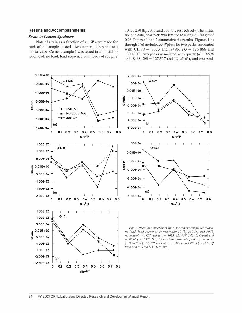
94 FY 2003 ORNL Laboratory Directed Research and Development Annual Report
Results and AccomplishmentsStrain in Cement Specimens
Plots of strain as a function of sin2Ψ were made foreach of the samples tested—two cement cubes and onemortar cube. Cement sample 1 was tested in an initial noload, load, no load, load sequence with loads of roughly
10 lbf, 250 lbf, 20 lbf and 300 lbf , respectively. The initialno load data, however, was limited to a single Ψ angle of0.0°. Figures 1 and 2 summarize the results. Figures 1(a)through 1(e) include sin2Ψ plots for two peaks associatedwith CH (d = .8623 and .8496, 2Θ = 126.866 and130.430°), two peaks associated with quartz (d = .8598and .8458, 2Θ = 127.537 and 131.516°), and one peak
Fig. 1. Strain as a function of sin2Ψ for cement sample for a load,no load, load sequence at nominally 10 lbf, 250 lbf, and 20 lbfrespectively: (a) CH peak at d = .8623 (126.866° 2Θ), (b) Q peak at d= .8598 (127.537° 2Θ), (c) calcium carbonate peak at d = .8571(128.262° 2Θ), (d) CH peak at d = .8495 (130.430° 2Θ), and (e) Qpeak at d = .9458 (131.516° 2Θ).
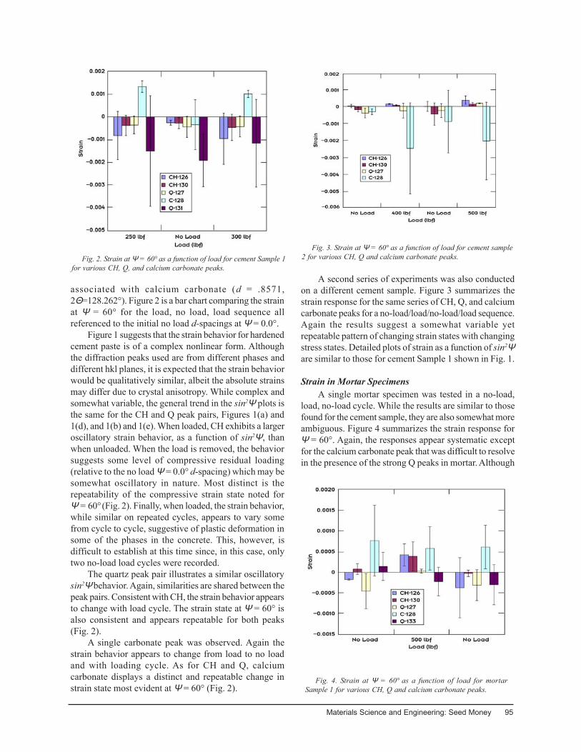
Materials Science and Engineering: Seed Money 95
associated with calcium carbonate (d = .8571,2Θ=128.262°). Figure 2 is a bar chart comparing the strainat Ψ = 60° for the load, no load, load sequence allreferenced to the initial no load d-spacings at Ψ = 0.0°.
Figure 1 suggests that the strain behavior for hardenedcement paste is of a complex nonlinear form. Althoughthe diffraction peaks used are from different phases anddifferent hkl planes, it is expected that the strain behaviorwould be qualitatively similar, albeit the absolute strainsmay differ due to crystal anisotropy. While complex andsomewhat variable, the general trend in the sin2Ψ plots isthe same for the CH and Q peak pairs, Figures 1(a) and1(d), and 1(b) and 1(e). When loaded, CH exhibits a largeroscillatory strain behavior, as a function of sin2Ψ, thanwhen unloaded. When the load is removed, the behaviorsuggests some level of compressive residual loading(relative to the no load Ψ = 0.0° d-spacing) which may besomewhat oscillatory in nature. Most distinct is therepeatability of the compressive strain state noted forΨ = 60° (Fig. 2). Finally, when loaded, the strain behavior,while similar on repeated cycles, appears to vary somefrom cycle to cycle, suggestive of plastic deformation insome of the phases in the concrete. This, however, isdifficult to establish at this time since, in this case, onlytwo no-load load cycles were recorded.
The quartz peak pair illustrates a similar oscillatorysin2Ψ behavior. Again, similarities are shared between thepeak pairs. Consistent with CH, the strain behavior appearsto change with load cycle. The strain state at Ψ = 60° isalso consistent and appears repeatable for both peaks(Fig. 2).
A single carbonate peak was observed. Again thestrain behavior appears to change from load to no loadand with loading cycle. As for CH and Q, calciumcarbonate displays a distinct and repeatable change instrain state most evident at Ψ = 60° (Fig. 2).
A second series of experiments was also conductedon a different cement sample. Figure 3 summarizes thestrain response for the same series of CH, Q, and calciumcarbonate peaks for a no-load/load/no-load/load sequence.Again the results suggest a somewhat variable yetrepeatable pattern of changing strain states with changingstress states. Detailed plots of strain as a function of sin2Ψare similar to those for cement Sample 1 shown in Fig. 1.
Strain in Mortar SpecimensA single mortar specimen was tested in a no-load,
load, no-load cycle. While the results are similar to thosefound for the cement sample, they are also somewhat moreambiguous. Figure 4 summarizes the strain response forΨ = 60°. Again, the responses appear systematic exceptfor the calcium carbonate peak that was difficult to resolvein the presence of the strong Q peaks in mortar. Although
Fig. 2. Strain at Ψ = 60° as a function of load for cement Sample 1for various CH, Q, and calcium carbonate peaks.
Fig. 4. Strain at Ψ = 60° as a function of load for mortarSample 1 for various CH, Q and calcium carbonate peaks.
Fig. 3. Strain at Ψ = 60° as a function of load for cement sample2 for various CH, Q and calcium carbonate peaks.
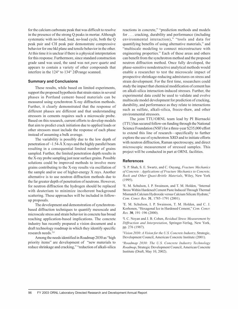
96 FY 2003 ORNL Laboratory Directed Research and Development Annual Report
for the calcium carbonate peak that was difficult to resolvein the presence of the strong Q peaks in mortar. Althoughsystematic with no-load, load, no-load cycle, both the Qpeak pair and CH peak pair demonstrate compressivebehavior for one hkl plane and tensile behavior in the other.At this time it is unclear if there is a physical interpretationfor this response. Furthermore, since standard constructiongrade sand was used, the sand was not pure quartz andappears to contain a variety of other compounds thatinterfere in the 124° to 134° 2Θ range scanned.
Summary and ConclusionsThese results, while based on limited experiments,
support the proposed hypothesis that strain states in severalphases in Portland cement–based materials can bemeasured using synchrotron X-ray diffraction methods.Further, it clearly demonstrated that the response ofdifferent phases are different and that understandingstressors in cements requires such a microscale probe.Based on this research, current efforts to develop modelsthat aim to predict crack initiation due to applied loads orother stressors must include the response of each phaseinstead of assuming a bulk average.
The variability is possibly due to the low depth ofpenetration of ~1.54-Å X rays and the highly parallel beamresulting in a consequential limited number of grainssampled. Further, the limited penetration depth results inthe X-ray probe sampling just near surface grains. Possiblesolutions could be improved methods to involve moregrains contributing to the X-ray results via oscillation ofthe sample and/or use of higher-energy X rays. Anotheralternative is to use neutron diffraction methods due tothe far greater depth of penetration of neutrons. However,for neutron diffraction the hydrogen should be replacedwith deuterium to minimize incoherent backgroundscattering. These approaches will be included in follow-up proposals.
The development and demonstration of synchrotron-based diffraction techniques to quantify mesoscale andmicroscale stress and strain behavior in concrete has broadreaching application-based implications. The concreteindustry has recently prepared a vision document and adraft technology roadmap in which they identify specificresearch needs.5,6
Among the needs identified in Roadmap 2030 as “highpriority items” are development of “new materials toreduce shrinkage and cracking,” “reduction of alkali-silica
reactions in concrete,” “prediction methods and modelsfor . . . cracking, durability and performance (includingenvironmental interaction),” “tools and data forquantifying benefits of using alternative materials,” and“multiscale modeling to connect microstructure withengineering properties.” Each of these areas and otherscan benefit from the synchrotron method and the proposedneutron diffraction method. Once fully developed, thephase-sensitive nondestructive analytical methods wouldenable a researcher to test the microscale impact ofprospective shrinkage-reducing admixtures on stress andstrain development. For the first time, researchers couldstudy the impact that chemical modification of cement hason alkali-silica interaction-induced stresses. Further, theexperimental data could be used to validate and evolvemultiscale model development for prediction of cracking,durability, and performance as they relate to interactionssuch as sulfate, alkali-silica, freeze-thaw, and otherenvironmental stressors.
The joint TTU/ORNL team lead by PI Biernacki(TTU) has secured follow-on funding through the NationalScience Foundation (NSF) for a three-year $235,000 effortto extend this line of research—specifically to furtherexplore the use of synchrotron XRD and to initiate effortswith neutron diffraction, Raman spectroscopy, and directmicroscopic measurement of stressed samples. Thisproject will be conducted in part at ORNL facilities.
References1S. P. Shah, S. E. Swartz, and C. Ouyang, Fracture Mechanicsof Concrete : Applications of Fracture Mechanics to Concrete,Rock and Other Quasi-Brittle Materials, Wiley, New York(1995).2E. M. Schulson, I. P. Swainson, and T. M. Holden, “InternalStress Within Hardened Cement Paste Induced Through ThermalMismatch Calcium Hydroxide versus Calcium Silicate Hydrate,”Cem. Concr. Res. 31, 1785–1791 (2001).3E. M. Schulson, I. P. Swainson, T. M. Holden, and C. J.Korhonen, “Hexagonal Ice in Hardened Cement,” Cem. Concr.Res. 30, 191–196 (2000).4I. C. Noyan and J. B. Cohen, Residual Stress Measurement byDiffraction and Interpretation, Springer-Verlag, New York,pp. 276 (1987).5Vision 2030: A Vision for the U.S. Concrete Industry, Strategic,Development Council, American Concrete Institute (2001).6Roadmap 2030: The U.S. Concrete Industry TechnologyRoadmap, Strategic Development Council, American ConcreteInstitute (Draft, May 10, 2002).
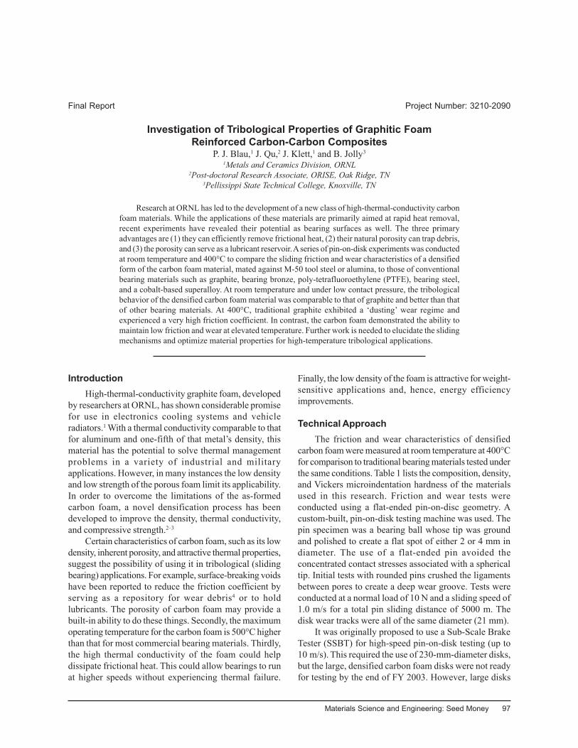
Materials Science and Engineering: Seed Money 97
Final Report Project Number: 3210-2090
Investigation of Tribological Properties of Graphitic FoamReinforced Carbon-Carbon Composites
P. J. Blau,1 J. Qu,2 J. Klett,1 and B. Jolly3
1Metals and Ceramics Division, ORNL2Post-doctoral Research Associate, ORISE, Oak Ridge, TN
3Pellissippi State Technical College, Knoxville, TN
Research at ORNL has led to the development of a new class of high-thermal-conductivity carbonfoam materials. While the applications of these materials are primarily aimed at rapid heat removal,recent experiments have revealed their potential as bearing surfaces as well. The three primaryadvantages are (1) they can efficiently remove frictional heat, (2) their natural porosity can trap debris,and (3) the porosity can serve as a lubricant reservoir. A series of pin-on-disk experiments was conductedat room temperature and 400°C to compare the sliding friction and wear characteristics of a densifiedform of the carbon foam material, mated against M-50 tool steel or alumina, to those of conventionalbearing materials such as graphite, bearing bronze, poly-tetrafluoroethylene (PTFE), bearing steel,and a cobalt-based superalloy. At room temperature and under low contact pressure, the tribologicalbehavior of the densified carbon foam material was comparable to that of graphite and better than thatof other bearing materials. At 400°C, traditional graphite exhibited a ‘dusting’ wear regime andexperienced a very high friction coefficient. In contrast, the carbon foam demonstrated the ability tomaintain low friction and wear at elevated temperature. Further work is needed to elucidate the slidingmechanisms and optimize material properties for high-temperature tribological applications.
IntroductionHigh-thermal-conductivity graphite foam, developed
by researchers at ORNL, has shown considerable promisefor use in electronics cooling systems and vehicleradiators.1 With a thermal conductivity comparable to thatfor aluminum and one-fifth of that metal’s density, thismaterial has the potential to solve thermal managementproblems in a variety of industrial and militaryapplications. However, in many instances the low densityand low strength of the porous foam limit its applicability.In order to overcome the limitations of the as-formedcarbon foam, a novel densification process has beendeveloped to improve the density, thermal conductivity,and compressive strength.2–3
Certain characteristics of carbon foam, such as its lowdensity, inherent porosity, and attractive thermal properties,suggest the possibility of using it in tribological (slidingbearing) applications. For example, surface-breaking voidshave been reported to reduce the friction coefficient byserving as a repository for wear debris4 or to holdlubricants. The porosity of carbon foam may provide abuilt-in ability to do these things. Secondly, the maximumoperating temperature for the carbon foam is 500°C higherthan that for most commercial bearing materials. Thirdly,the high thermal conductivity of the foam could helpdissipate frictional heat. This could allow bearings to runat higher speeds without experiencing thermal failure.
Finally, the low density of the foam is attractive for weight-sensitive applications and, hence, energy efficiencyimprovements.
Technical ApproachThe friction and wear characteristics of densified
carbon foam were measured at room temperature at 400°Cfor comparison to traditional bearing materials tested underthe same conditions. Table 1 lists the composition, density,and Vickers microindentation hardness of the materialsused in this research. Friction and wear tests wereconducted using a flat-ended pin-on-disc geometry. Acustom-built, pin-on-disk testing machine was used. Thepin specimen was a bearing ball whose tip was groundand polished to create a flat spot of either 2 or 4 mm indiameter. The use of a flat-ended pin avoided theconcentrated contact stresses associated with a sphericaltip. Initial tests with rounded pins crushed the ligamentsbetween pores to create a deep wear groove. Tests wereconducted at a normal load of 10 N and a sliding speed of1.0 m/s for a total pin sliding distance of 5000 m. Thedisk wear tracks were all of the same diameter (21 mm).
It was originally proposed to use a Sub-Scale BrakeTester (SSBT) for high-speed pin-on-disk testing (up to10 m/s). This required the use of 230-mm-diameter disks,but the large, densified carbon foam disks were not readyfor testing by the end of FY 2003. However, large disks
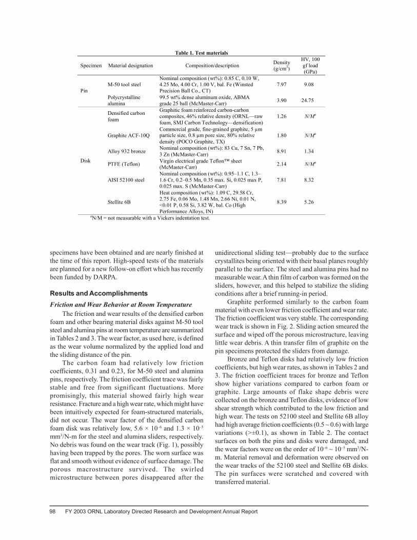
98 FY 2003 ORNL Laboratory Directed Research and Development Annual Report
specimens have been obtained and are nearly finished atthe time of this report. High-speed tests of the materialsare planned for a new follow-on effort which has recentlybeen funded by DARPA.
Results and AccomplishmentsFriction and Wear Behavior at Room Temperature
The friction and wear results of the densified carbonfoam and other bearing material disks against M-50 toolsteel and alumina pins at room temperature are summarizedin Tables 2 and 3. The wear factor, as used here, is definedas the wear volume normalized by the applied load andthe sliding distance of the pin.
The carbon foam had relatively low frictioncoefficients, 0.31 and 0.23, for M-50 steel and aluminapins, respectively. The friction coefficient trace was fairlystable and free from significant fluctuations. Morepromisingly, this material showed fairly high wearresistance. Fracture and a high wear rate, which might havebeen intuitively expected for foam-structured materials,did not occur. The wear factor of the densified carbonfoam disk was relatively low, 5.6 × 10⁻⁶ and 1.3 × 10⁻⁵
mm3/N-m for the steel and alumina sliders, respectively.No debris was found on the wear track (Fig. 1), possiblyhaving been trapped by the pores. The worn surface wasflat and smooth without evidence of surface damage. Theporous macrostructure survived. The swirledmicrostructure between pores disappeared after the
unidirectional sliding test—probably due to the surfacecrystallites being oriented with their basal planes roughlyparallel to the surface. The steel and alumina pins had nomeasurable wear. A thin film of carbon was formed on thesliders, however, and this helped to stabilize the slidingconditions after a brief running-in period.
Graphite performed similarly to the carbon foammaterial with even lower friction coefficient and wear rate.The friction coefficient was very stable. The correspondingwear track is shown in Fig. 2. Sliding action smeared thesurface and wiped off the porous microstructure, leavinglittle wear debris. A thin transfer film of graphite on thepin specimens protected the sliders from damage.
Bronze and Teflon disks had relatively low frictioncoefficients, but high wear rates, as shown in Tables 2 and3. The friction coefficient traces for bronze and Teflonshow higher variations compared to carbon foam orgraphite. Large amounts of flake shape debris werecollected on the bronze and Teflon disks, evidence of lowshear strength which contributed to the low friction andhigh wear. The tests on 52100 steel and Stellite 6B alloyhad high average friction coefficients (0.5 ~ 0.6) with largevariations (>±0.1), as shown in Table 2. The contactsurfaces on both the pins and disks were damaged, andthe wear factors were on the order of 10–6 ~ 10–5 mm3/N-m. Material removal and deformation were observed onthe wear tracks of the 52100 steel and Stellite 6B disks.The pin surfaces were scratched and covered withtransferred material.
Table 1. Test materials
Specimen Material designation Composition/description Density (g/cm3)
HV, 100 gf load (GPa)
M-50 tool steel Nominal composition (wt%): 0.85 C, 0.10 W, 4.25 Mo, 4.00 Cr, 1.00 V, bal. Fe (Winsted Precision Ball Co., CT)
7.97 9.08 Pin
Polycrystalline alumina
99.5 wt% dense aluminum oxide, ABMA grade 25 ball (McMaster-Carr) 3.90 24.75
Densified carbon foam
Graphitic foam reinforced carbon-carbon composites, 46% relative density (ORNL—raw foam, SMJ Carbon Technology—densification)
1.26 N/Ma
Graphite ACF-10Q Commercial grade, fine-grained graphite, 5 µm particle size, 0.8 µm pore size, 80% relative density (POCO Graphite, TX)
1.80 N/Ma
Alloy 932 bronze Nominal composition (wt%): 83 Cu, 7 Sn, 7 Pb, 3 Zn (McMaster-Carr) 8.91 1.34
PTFE (Teflon) Virgin electrical grade Teflon™ sheet (McMaster-Carr) 2.14 N/Ma
AISI 52100 steel Nominal composition (wt%): 0.95–1.1 C, 1.3–1.6 Cr, 0.2–0.5 Mn, 0.35 max. Si, 0.025 max P, 0.025 max. S (McMaster-Carr)
7.81 8.32
Disk
Stellite 6B
Heat composition (wt%): 1.09 C, 29.58 Cr, 2.75 Fe, 0.06 Mo, 1.48 Mn, 2.66 Ni, 0.01 N, <0.01 P, 0.58 Si, 3.82 W, bal. Co (High Performance Alloys, IN)
8.39 5.26
aN/M = not measurable with a Vickers indentation test.
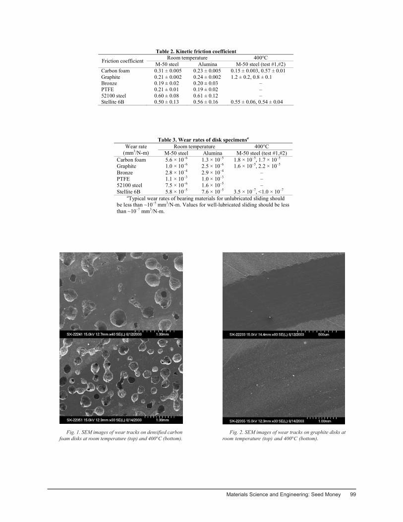
Materials Science and Engineering: Seed Money 99
Fig. 1. SEM images of wear tracks on densified carbonfoam disks at room temperature (top) and 400°C (bottom).
Fig. 2. SEM images of wear tracks on graphite disks atroom temperature (top) and 400°C (bottom).
Table 2. Kinetic friction coefficient Room temperature 400°C Friction coefficient M-50 steel Alumina M-50 steel (test #1,#2)
Carbon foam 0.31 ± 0.005 0.23 ± 0.005 0.15 ± 0.003, 0.57 ± 0.01 Graphite 0.21 ± 0.002 0.24 ± 0.002 1.2 ± 0.2, 0.8 ± 0.1 Bronze 0.19 ± 0.02 0.20 ± 0.03 – PTFE 0.21 ± 0.01 0.19 ± 0.02 – 52100 steel 0.60 ± 0.08 0.61 ± 0.12 – Stellite 6B 0.50 ± 0.13 0.56 ± 0.16 0.55 ± 0.06, 0.54 ± 0.04
Table 3. Wear rates of disk specimensa Room temperature 400°C Wear rate
(mm3/N-m) M-50 steel Alumina M-50 steel (test #1,#2) Carbon foam 5.6 × 10⁻⁶ 1.3 × 10⁻⁵ 1.8 × 10⁻⁵, 1.7 × 10⁻⁵ Graphite 1.0 × 10⁻⁶ 2.5 × 10⁻⁶ 1.6 × 10⁻⁵, 2.2 × 10⁻⁵ Bronze 2.8 × 10⁻⁴ 2.9 × 10⁻⁴ – PTFE 1.1 × 10⁻³ 1.0 × 10⁻³ – 52100 steel 7.5 × 10⁻⁶ 1.6 × 10⁻⁵ – Stellite 6B 5.8 × 10⁻⁵ 7.6 × 10⁻⁵ 3.5 × 10⁻⁷, <1.0 × 10⁻⁷
aTypical wear rates of bearing materials for unlubricated sliding should be less than ~10–5 mm3/N-m. Values for well-lubricated sliding should be less than ~10–7 mm3/N-m.
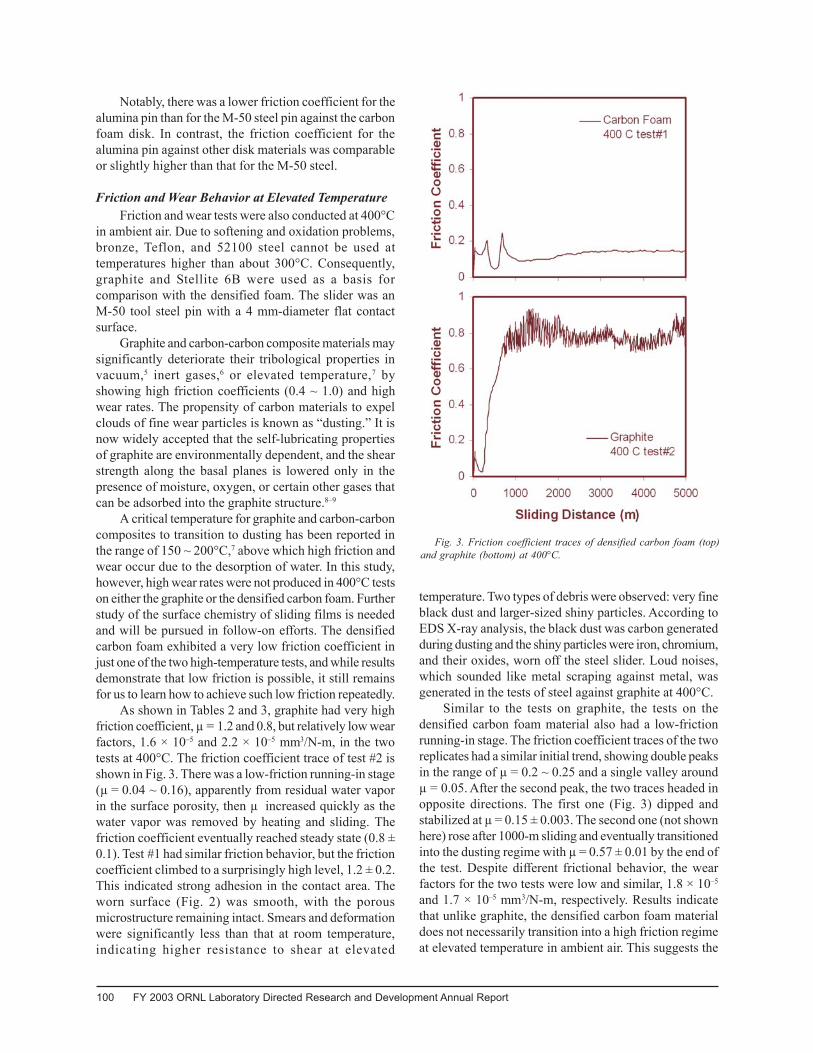
100 FY 2003 ORNL Laboratory Directed Research and Development Annual Report
Notably, there was a lower friction coefficient for thealumina pin than for the M-50 steel pin against the carbonfoam disk. In contrast, the friction coefficient for thealumina pin against other disk materials was comparableor slightly higher than that for the M-50 steel.
Friction and Wear Behavior at Elevated TemperatureFriction and wear tests were also conducted at 400°C
in ambient air. Due to softening and oxidation problems,bronze, Teflon, and 52100 steel cannot be used attemperatures higher than about 300°C. Consequently,graphite and Stellite 6B were used as a basis forcomparison with the densified foam. The slider was anM-50 tool steel pin with a 4 mm-diameter flat contactsurface.
Graphite and carbon-carbon composite materials maysignificantly deteriorate their tribological properties invacuum,5 inert gases,6 or elevated temperature,7 byshowing high friction coefficients (0.4 ~ 1.0) and highwear rates. The propensity of carbon materials to expelclouds of fine wear particles is known as “dusting.” It isnow widely accepted that the self-lubricating propertiesof graphite are environmentally dependent, and the shearstrength along the basal planes is lowered only in thepresence of moisture, oxygen, or certain other gases thatcan be adsorbed into the graphite structure.8–9
A critical temperature for graphite and carbon-carboncomposites to transition to dusting has been reported inthe range of 150 ~ 200°C,7 above which high friction andwear occur due to the desorption of water. In this study,however, high wear rates were not produced in 400°C testson either the graphite or the densified carbon foam. Furtherstudy of the surface chemistry of sliding films is neededand will be pursued in follow-on efforts. The densifiedcarbon foam exhibited a very low friction coefficient injust one of the two high-temperature tests, and while resultsdemonstrate that low friction is possible, it still remainsfor us to learn how to achieve such low friction repeatedly.
As shown in Tables 2 and 3, graphite had very highfriction coefficient, µ = 1.2 and 0.8, but relatively low wearfactors, 1.6 × 10⁻⁵ and 2.2 × 10⁻⁵ mm3/N-m, in the twotests at 400°C. The friction coefficient trace of test #2 isshown in Fig. 3. There was a low-friction running-in stage(µ = 0.04 ~ 0.16), apparently from residual water vaporin the surface porosity, then µ increased quickly as thewater vapor was removed by heating and sliding. Thefriction coefficient eventually reached steady state (0.8 ±0.1). Test #1 had similar friction behavior, but the frictioncoefficient climbed to a surprisingly high level, 1.2 ± 0.2.This indicated strong adhesion in the contact area. Theworn surface (Fig. 2) was smooth, with the porousmicrostructure remaining intact. Smears and deformationwere significantly less than that at room temperature,indicating higher resistance to shear at elevated
temperature. Two types of debris were observed: very fineblack dust and larger-sized shiny particles. According toEDS X-ray analysis, the black dust was carbon generatedduring dusting and the shiny particles were iron, chromium,and their oxides, worn off the steel slider. Loud noises,which sounded like metal scraping against metal, wasgenerated in the tests of steel against graphite at 400°C.
Similar to the tests on graphite, the tests on thedensified carbon foam material also had a low-frictionrunning-in stage. The friction coefficient traces of the tworeplicates had a similar initial trend, showing double peaksin the range of µ = 0.2 ~ 0.25 and a single valley aroundµ = 0.05. After the second peak, the two traces headed inopposite directions. The first one (Fig. 3) dipped andstabilized at µ = 0.15 ± 0.003. The second one (not shownhere) rose after 1000-m sliding and eventually transitionedinto the dusting regime with µ = 0.57 ± 0.01 by the end ofthe test. Despite different frictional behavior, the wearfactors for the two tests were low and similar, 1.8 × 10⁻⁵
and 1.7 × 10⁻⁵ mm3/N-m, respectively. Results indicatethat unlike graphite, the densified carbon foam materialdoes not necessarily transition into a high friction regimeat elevated temperature in ambient air. This suggests the
Fig. 3. Friction coefficient traces of densified carbon foam (top)and graphite (bottom) at 400°C.
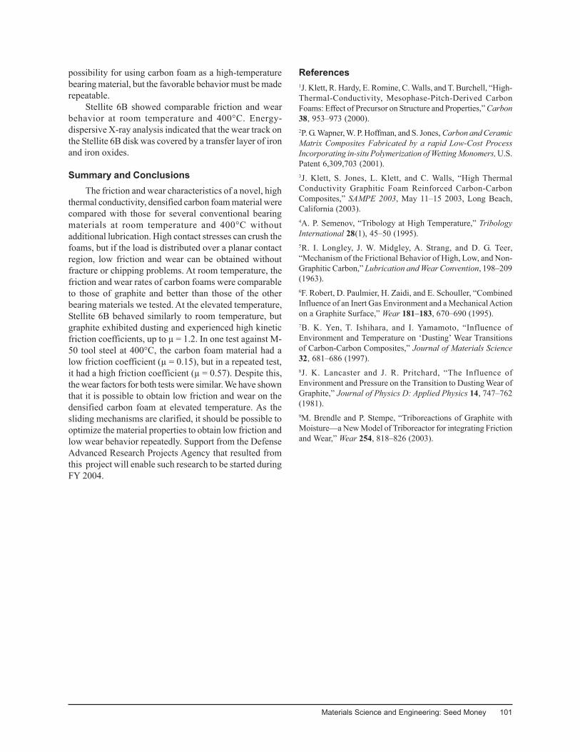
Materials Science and Engineering: Seed Money 101
possibility for using carbon foam as a high-temperaturebearing material, but the favorable behavior must be maderepeatable.
Stellite 6B showed comparable friction and wearbehavior at room temperature and 400°C. Energy-dispersive X-ray analysis indicated that the wear track onthe Stellite 6B disk was covered by a transfer layer of ironand iron oxides.
Summary and ConclusionsThe friction and wear characteristics of a novel, high
thermal conductivity, densified carbon foam material werecompared with those for several conventional bearingmaterials at room temperature and 400°C withoutadditional lubrication. High contact stresses can crush thefoams, but if the load is distributed over a planar contactregion, low friction and wear can be obtained withoutfracture or chipping problems. At room temperature, thefriction and wear rates of carbon foams were comparableto those of graphite and better than those of the otherbearing materials we tested. At the elevated temperature,Stellite 6B behaved similarly to room temperature, butgraphite exhibited dusting and experienced high kineticfriction coefficients, up to µ = 1.2. In one test against M-50 tool steel at 400°C, the carbon foam material had alow friction coefficient (µ = 0.15), but in a repeated test,it had a high friction coefficient (µ = 0.57). Despite this,the wear factors for both tests were similar. We have shownthat it is possible to obtain low friction and wear on thedensified carbon foam at elevated temperature. As thesliding mechanisms are clarified, it should be possible tooptimize the material properties to obtain low friction andlow wear behavior repeatedly. Support from the DefenseAdvanced Research Projects Agency that resulted fromthis project will enable such research to be started duringFY 2004.
References1J. Klett, R. Hardy, E. Romine, C. Walls, and T. Burchell, “High-Thermal-Conductivity, Mesophase-Pitch-Derived CarbonFoams: Effect of Precursor on Structure and Properties,” Carbon38, 953–973 (2000).2P. G. Wapner, W. P. Hoffman, and S. Jones, Carbon and CeramicMatrix Composites Fabricated by a rapid Low-Cost ProcessIncorporating in-situ Polymerization of Wetting Monomers, U.S.Patent 6,309,703 (2001).3J. Klett, S. Jones, L. Klett, and C. Walls, “High ThermalConductivity Graphitic Foam Reinforced Carbon-CarbonComposites,” SAMPE 2003, May 11–15 2003, Long Beach,California (2003).4A. P. Semenov, “Tribology at High Temperature,” TribologyInternational 28(1), 45–50 (1995).5R. I. Longley, J. W. Midgley, A. Strang, and D. G. Teer,“Mechanism of the Frictional Behavior of High, Low, and Non-Graphitic Carbon,” Lubrication and Wear Convention, 198–209(1963).6F. Robert, D. Paulmier, H. Zaidi, and E. Schouller, “CombinedInfluence of an Inert Gas Environment and a Mechanical Actionon a Graphite Surface,” Wear 181–183, 670–690 (1995).7B. K. Yen, T. Ishihara, and I. Yamamoto, “Influence ofEnvironment and Temperature on ‘Dusting’ Wear Transitionsof Carbon-Carbon Composites,” Journal of Materials Science32, 681–686 (1997).8J. K. Lancaster and J. R. Pritchard, “The Influence ofEnvironment and Pressure on the Transition to Dusting Wear ofGraphite,” Journal of Physics D: Applied Physics 14, 747–762(1981).9M. Brendle and P. Stempe, “Triboreactions of Graphite withMoisture—a New Model of Triboreactor for integrating Frictionand Wear,” Wear 254, 818–826 (2003).
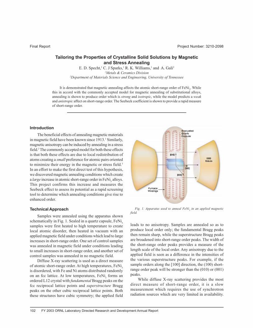
102 FY 2003 ORNL Laboratory Directed Research and Development Annual Report
Final Report Project Number: 3210-2098
Tailoring the Properties of Crystalline Solid Solutions by Magneticand Stress Annealing
E. D. Specht,1 C. J Sparks,1 R. K. Williams,1 and A. Gali2
1Metals & Ceramics Division2Department of Materials Science and Engineering, University of Tennessee
It is demonstrated that magnetic annealing affects the atomic short-range order of FeNi3. Whilethis in accord with the commonly accepted model for magnetic annealing of substitutional alloys,annealing is shown to produce order which is strong and isotropic, while the model predicts a weakand anistropic affect on short-range order. The Seebeck coefficient is shown to provide a rapid measureof short-range order.
IntroductionThe beneficial effects of annealing magnetic materials
in magnetic field have been known since 1913.1 Similarly,magnetic anisotropy can be induced by annealing in a stressfield.2 The commonly accepted model for both these effectsis that both these effects are due to local redistribution ofatoms creating a small preference for atomic pairs orientedto minimize their energy in the magnetic or stress field.3
In an effort to make the first direct test of this hypothesis,we discovered magnetic annealing conditions which createa large increase in atomic short-range order in FeNi3 alloys.This project confirms this increase and measures theSeebeck effect to assess its potential as a rapid screeningtool to determine which annealing conditions give rise toenhanced order.
Technical ApproachSamples were annealed using the apparatus shown
schematically in Fig. 1. Sealed in a quartz capsule, FeNi3samples were first heated to high temperature to createlocal atomic disorder, then heated in vacuum with anapplied magnetic field under conditions which lead to largeincreases in short-range order. One set of control sampleswas annealed in magnetic field under conditions leadingto small increases in short-range order, and another set ofcontrol samples was annealed in no magnetic field.
Diffuse X-ray scattering is used as a direct measureof atomic short-range order. At high temperatures, FeNi3is disordered, with Fe and Ni atoms distributed randomlyon an fcc lattice. At low temperatures, FeNi3 forms anordered L12 crystal with fundamental Bragg peaks on thefcc reciprocal lattice points and superstructure Braggpeaks on the other cubic reciprocal lattice points. Boththese structures have cubic symmetry; the applied field
leads to no anisotropy. Samples are annealed so as toproduce local order only; the fundamental Bragg peaksthen remain sharp, while the superstructure Bragg peaksare broadened into short-range order peaks. The width ofthe short-range order peaks provides a measure of thelength scale of the local order. Any anisotropy due to theapplied field is seen as a difference in the intensities ofthe various superstructure peaks. For example, if thesample orders along the [100] direction, the (100) short-range order peak will be stronger than the (010) or (001)peaks.
While diffuse X-ray scattering provides the mostdirect measure of short-range order, it is a slowmeasurement which requires the use of synchrotronradiation sources which are very limited in availability.
Fig. 1. Apparatus used to anneal FeNi3 in an applied magneticfield.
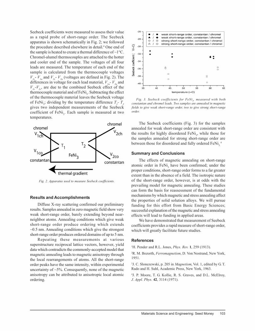
Materials Science and Engineering: Seed Money 103
Seebeck coefficients were measured to assess their valueas a rapid probe of short-range order. The Seebeckapparatus is shown schematically in Fig. 2; we followedthe procedure described elsewhere in detail.4 One end ofthe sample is heated to create a thermal difference of ~1°C.Chromel-alumel thermocouples are attached to the hotterand cooler end of the sample. The voltages of all fourleads are measured. The temperature of each end of thesample is calculated from the thermocouple voltagesV1c- V1a and V2c- V2a (voltages are defined in Fig. 2). Thedifferences in voltage for each lead material, V1a- V2a andV1c-V2c, are due to the combined Seebeck effect of thethermocouple material and of FeNi3. Subtracting the effectof the thermocouple material leaves the Seebeck voltageof FeNi3; dividing by the temperature difference T1- T2gives two independent measurements of the Seebeckcoefficient of FeNi3. Each sample is measured at twotemperatures.
Results and AccomplishmentsDiffuse X-ray scattering confirmed our preliminary
results. Samples annealed in zero magnetic field show veryweak short-range order, barely extending beyond near-neighbor atoms. Annealing conditions which give weakshort-range order produce ordering which extends~0.5 nm. Annealing conditions which give the strongestshort-range order produces ordered domains of up to 5 nm.
Repeating these measurements at varioussuperstructure reciprocal lattice vectors, however, yielddata which contradicts the commonly-accepted model thatmagnetic annealing leads to magnetic anisotropy throughthe local rearrangements of atoms. All the short-rangeorder peaks have the same intensity, within experimentaluncertainty of ~5%. Consequently, none of the magneticanisotropy can be attributed to anisotropic local atomicordering.
Fig. 3. Seebeck coefficients for FeNi3, measured with bothconstantan and chromel leads. Two samples are annealed in magneticfields to give weak short-range order, two to give strong short-rangeorder.
Fig. 2. Apparatus used to measure Seebeck coefficients.
The Seebeck coefficients (Fig. 3) for the samplesannealed for weak short-range order are consistent withthe results for highly disordered FeNi3, while those forthe samples annealed for strong short-range order arebetween those for disordered and fully ordered FeNi3.
4
Summary and ConclusionsThe effects of magnetic annealing on short-range
atomic order in FeNi3 have been confirmed; under theproper conditions, short-range order forms to a far greaterextent than in the absence of a field. The isotropic natureof the short-range order, however, is at odds with theprevailing model for magnetic annealing. These studiescan form the basis for reassessment of the fundamentalmechanisms by which magnetic and stress annealing affectthe properties of solid solution alloys. We will pursuefunding for this effort from Basic Energy Sciences;successful explanation of the magnetic and stress annealingeffects will lead to funding in applied areas.
We have demonstrated that measurement of Seebeckcoefficients provides a rapid measure of short-range order,which will greatly facilitate future studies.
References1H. Pender and R.L. Jones, Phys. Rev. 1, 259 (1913).2R. M. Bozorth, Ferromagnetism, D. Von Nostrand, New York,1951.3J. C. Slonezewski, p. 205 in Magnetism, Vol. 1, edited by G. T.Rado and H. Suhl, Academic Press, New York, 1963.4J. P. Moore, T. G. Kollie, R. S. Graves, and D.L. McElroy,J. Appl. Phys. 42, 3114 (1971).
104 FY 2003 ORNL Laboratory Directed Research and Development Annual Report
Progress Report Project Number 3210-2057
Nanoelectronic Devices Made from Doped NanofibersJ. B. O. Caughman,1 M. L. Guillorn,2 D. B. Beach,3 V. I. Merkulov,2 L. R. Baylor,1 and L. F. Allard4
1Fusion Energy Division2Engineering Science and Technology Division
3Chemical Sciences Division4Metals and Ceramics Division
The purpose of this project is to understand and develop a process for depositing doped carbonand boron carbonitride nanofibers that will be used to make nanoelectronic devices in a way that willbe useful for large-scale manufacturing. Vertically aligned nanofibers are being grown using a high-density plasma-enhanced chemical vapor deposition technique that allows control of gas-phase andsurface chemistry. In contrast to current growth methods, the electrical properties of the nanofiberswill be controlled by substitutional doping of boron and/or nitrogen to produce metallic orsemiconducting doped carbon or boron carbonitride nanofibers. The electrical characteristics ofindividual vertical nanofibers will be determined by measuring the current flowing through the fiberas a function of applied voltage across the fiber. Nanofiber rectifying devices containing metal-semiconductor (Schottky) junctions will be grown and measured. Our approach for growing nanofibershas advantages over current methods in terms of controlling electrical properties of individualnanofibers, controlling the geometry of the growth, and the potential use as a practical method forrealizing vertical integration of dense arrays of nanoelectronics.
One of the main objectives of our project is to beable to control the electrical characteristics of nanofibersby controlling their composition. The other objective isto be able to grow individual, isolated nanofibers in acontrolled way. Such an approach has applications formassively parallel vertical nanofiber devices fornanoelectronics. Our approach for growth of the fibersuses a plasma-enhanced chemical vapor depositiontechnique using an inductively coupled radio frequencyplasma source operated at low pressure (<100 mTorr).The gases used during the growth process includehydrogen and a carbon-containing gas, which is eitheracetylene or methane. Details of the system and initialgrowth results can be found in a recently published paper(Caughman et al., J. Appl. Phys., Vol. 83, 2003, p. 1207).Our research to date has focused on understanding of thegrowth of vertically aligned carbon-based nanofibers andhow to change their composition. We have conductedexperiments to determine the role of various parameterson the growth results, started the electrical characterizationof the nanofibers, and are starting to explore changes totheir composition with the addition of boron.
Many parameters influence the growth and structureof vertically aligned carbon nanofibers (VACNFs),including the gas composition, the substrate bias, and thegrowth temperature. As the gas composition changes frombeing hydrogen rich to a carbon rich (i.e., by increasing
the acetylene flow relative to the hydrogen flow), thestructure of the fibers changes from being tall and thincylinders to broad-based cones. The carbon-rich plasmacondition creates excess carbon species that condense onthe sides of the fibers to create the cone-like structure.The role of substrate bias is related to ion energy, whichcontrols the physical etching that takes place duringVACNF growth. We have discovered that a minimumamount of substrate bias is required to grow fibers. If theion energies are too low, then a layer of carbon builds upon the surface and VACNF growth stops. We have alsodiscovered that growth temperature is important. If thegrowth temperature gets too high, then the carbon-containing gas (acetylene of methane) will substantiallydecompose on the substrate surface and inhibit VACNFgrowth. There is a balance between growth temperatureand gas flow. We have added an optical pyrometer to thesystem to better control the temperature during growth.
The electrical characterization of the VACNFs hasstarted. We have measured the VACNF conductivity byusing a four-point probe technique. We have found thatthe VACNFs are conducting, with a conductivity similarto graphite at 1 mΩ-cm, which is similar to that measuredfor VACNFs grown with a DC PECVD technique by MikeSimpson’s group at ORNL.
The changes to the fibers as a function of compositionare also being explored. For growing boron-containing
Materials Science and Engineering: Seed Money 105
VACNFs, we have added dilute diborane to the system(4% in hydrogen). Tests with the mass spectrometer haveshown that the plasma is very efficient at breaking up thediborane in the gas-phase, which is probably advantageousfor the boron to become bonded in the nanofiber structure(less surface temperature needed to break the chemicalbonds because the plasma already did it). High diboraneflows have been shown to inhibit nanofiber growth, whilelow flows do not. The change in nanofiber compositionas a function of diborane flow is currently beingdetermined.
There should be numerous benefits for DOE andpotential for follow-on funding. The area of nanoscienceis of great interest to DOE, and the knowledge that wegain from this work will help us to understand the growthmechanisms of nanofibers. Potential applications ofinterest include nanoelectronics, field-emission devices,hydrogen storage, and super-hydrophobic materials. Weare currently pursuing follow-on funding as part of a white-paper to DARPA.
106 FY 2003 ORNL Laboratory Directed Research and Development Annual Report
Progress Report Project Number: 3210-2069
Development of a New High-Temperature Proton-Electron Mixed Conductorfor Hydrogen Separation
E. A. Payzant, R. D. Carneim, S. A. Speakman, and T. R. ArmstrongMetals and Ceramics Division
High-temperature ion transport membranes (proton conductors) are presently limited in availabilityand performance. Current high-temperature proton conductors (HTPCs) either have low conductivities(e.g., SrZrO3-based materials) or are highly susceptible to chemical attack by contaminants such assulfur (H2S) and CO2 (e.g., BaCeO3-based materials). The purpose of the proposed research is todevelop a practical HTPC, where high conductivity is the primary requirement, based on a novelapproach investigating proton conductivity near phase boundaries. Durability is addressed by avoidingthe use of polyvalent lanthanides and transition metals, which bind readily with sulfur—especiallyunder the reducing conditions found in reformate or syngas streams. The perovskites LaYO3 andSrZrO3, and the pyrochlore La2Zr2O7, meet the stability requirement and have demonstrated protonconductivity. These binary oxides have low proton conductivities; however, by studying pyrochlore–perovskite binary systems, it was hoped a ternary composition will be produced that meets the primaryrequirement for a practical HTPC—high conductivity. This novel approach relies on there being atleast one phase boundary between the two end-point compositions. It is expected that various properties,including protonic conduction, of each end-point phase can be increased since transport mechanismsare often enhanced near phase boundaries. Rapid synthesis and characterization techniques are usedto screen a large number of initial compositions, which was followed by conductivity measurements,structural characterization, and modeling.
X-ray diffraction and dc conductivity measurementswere used to survey the functionality of two pyrochlore-perovskite binary systems as high-temperature protonconductors (HTPCs). An efficient HTPC could beemployed in a number of electrochemical devices, suchas gas separation membranes, fuel cells, or direct chemicalconversion stacks. The primary driver for HTPCdevelopment is the need for hydrogen separationmembranes that can provide an unadulterated hydrogenstream from a reformate feed for petrochemical processing.Equally important, though, are the advantages an efficientHTPC could provide to a future generation of fuel celltechnology.
A solid ceramic ion transport membrane has thegreatest potential for producing pure hydrogen at hightemperatures. Nafion® membranes produced by DuPontare currently the most effective low-temperature protonconductors; however, their maximum operatingtemperature (~160°C for hybrid membranes) is below thedesired operating temperature (500 to 600°C) forpetrochemical processes.1 Microporous membranesoperate in this temperature range with high fluxes;however, they are at best 99% selective to hydrogen.2Ceramic membranes operate well at high temperatures andcan be very selective; however, they are intolerant to H2Sand CO2 contaminants and their flux is too low for practical
application.2
Ionic conductivity in ceramics can be enhanced bydisorder. Typically, disorder is related to structural defectssuch as oxygen vacancies or to configurational featuressuch as the rotation and tilting of oxygen polyhedra.However, disorder can also be created by fluctuations incrystal structure. Displacive properties, such aspiezoelectricity, are enhanced at compositions near a phaseboundary, where little separates one phase from anotherand localized regions can dynamically fluctuate betweendifferent crystal structures.3 The inherent chaos of thesestructural fluctuations increases the kinetics of the system.It has recently been shown that transport properties canalso be enhanced at a phase boundary, providing a newmechanism for developing fast ion conduction in ceramicoxides.4
The crystal structure for pyrochlore, A2B2O7, hasoctahedrally coordinated B-site cations, 8 coordinated A-site cations, and two distinct oxygen sites. The crystalstructure of perovskite, ABO3, also has octahedrallycoordinated B-site cations, as well as 12 coordinated A-site cations. The pyrochlore-perovskite binary system waschosen for study because the crystal structures shareseveral features, particularly the BO6 octohedra.Additionally, small, localized regions of pyrochlore-typeordering were recently observed in perovskite materials.5
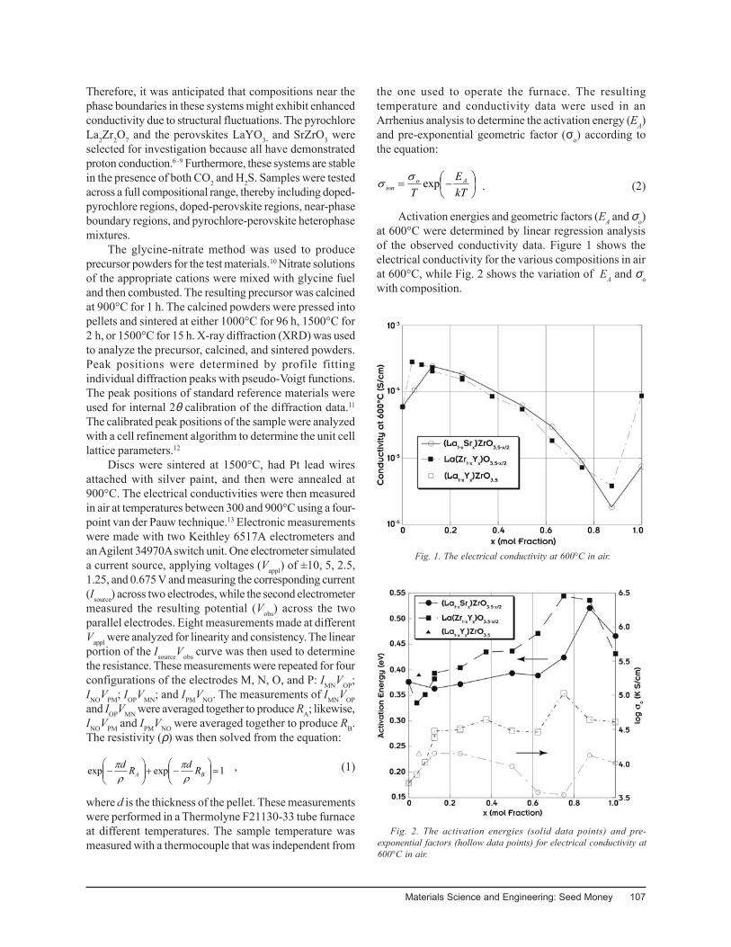
Materials Science and Engineering: Seed Money 107
Therefore, it was anticipated that compositions near thephase boundaries in these systems might exhibit enhancedconductivity due to structural fluctuations. The pyrochloreLa2Zr2O7 and the perovskites LaYO3- and SrZrO3 wereselected for investigation because all have demonstratedproton conduction.6–9 Furthermore, these systems are stablein the presence of both CO2 and H2S. Samples were testedacross a full compositional range, thereby including doped-pyrochlore regions, doped-perovskite regions, near-phaseboundary regions, and pyrochlore-perovskite heterophasemixtures.
The glycine-nitrate method was used to produceprecursor powders for the test materials.10 Nitrate solutionsof the appropriate cations were mixed with glycine fueland then combusted. The resulting precursor was calcinedat 900°C for 1 h. The calcined powders were pressed intopellets and sintered at either 1000°C for 96 h, 1500°C for2 h, or 1500°C for 15 h. X-ray diffraction (XRD) was usedto analyze the precursor, calcined, and sintered powders.Peak positions were determined by profile fittingindividual diffraction peaks with pseudo-Voigt functions.The peak positions of standard reference materials wereused for internal 2θ calibration of the diffraction data.11
The calibrated peak positions of the sample were analyzedwith a cell refinement algorithm to determine the unit celllattice parameters.12
Discs were sintered at 1500°C, had Pt lead wiresattached with silver paint, and then were annealed at900°C. The electrical conductivities were then measuredin air at temperatures between 300 and 900°C using a four-point van der Pauw technique.13 Electronic measurementswere made with two Keithley 6517A electrometers andan Agilent 34970A switch unit. One electrometer simulateda current source, applying voltages (Vappl) of ±10, 5, 2.5,1.25, and 0.675 V and measuring the corresponding current(Isource) across two electrodes, while the second electrometermeasured the resulting potential (Vobs) across the twoparallel electrodes. Eight measurements made at differentVappl were analyzed for linearity and consistency. The linearportion of the IsourceVobs curve was then used to determinethe resistance. These measurements were repeated for fourconfigurations of the electrodes M, N, O, and P: IMNVOP;INOVPM; IOPVMN; and IPMVNO. The measurements of IMNVOPand IOPVMN were averaged together to produce RA; likewise,INOVPM and IPMVNO were averaged together to produce RB.The resistivity (ρ) was then solved from the equation:
1expexp =
−+
− BA RdRd
ρπ
ρπ , (1)
where d is the thickness of the pellet. These measurementswere performed in a Thermolyne F21130-33 tube furnaceat different temperatures. The sample temperature wasmeasured with a thermocouple that was independent from
the one used to operate the furnace. The resultingtemperature and conductivity data were used in anArrhenius analysis to determine the activation energy (EA)and pre-exponential geometric factor (σo) according tothe equation:
−=
kTE
TAo
ion expσσ . (2)
Activation energies and geometric factors (EA and σo)at 600°C were determined by linear regression analysisof the observed conductivity data. Figure 1 shows theelectrical conductivity for the various compositions in airat 600°C, while Fig. 2 shows the variation of EA and σowith composition.
Fig. 1. The electrical conductivity at 600°C in air.
Fig. 2. The activation energies (solid data points) and pre-exponential factors (hollow data points) for electrical conductivity at600°C in air.
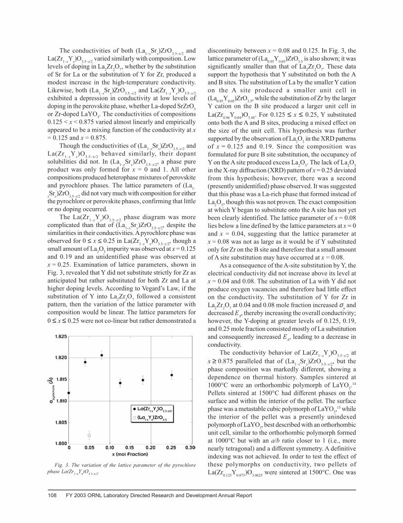
108 FY 2003 ORNL Laboratory Directed Research and Development Annual Report
The conductivities of both (La1–xSrx)ZrO3.5–x/2 andLa(Zr1–xYx)O3.5–x/2 varied similarly with composition. Lowlevels of doping in La2Zr2O7, whether by the substitutionof Sr for La or the substitution of Y for Zr, produced amodest increase in the high-temperature conductivity.Likewise, both (La1–xSrx)ZrO3.5–x/2 and La(Zr1–xYx)O3.5–x/2exhibited a depression in conductivity at low levels ofdoping in the perovskite phase, whether La-doped SrZrO3or Zr-doped LaYO3. The conductivities of compositions0.125 < x < 0.875 varied almost linearly and empiricallyappeared to be a mixing function of the conductivity at x= 0.125 and x = 0.875.
Though the conductivities of (La1–xSrx)ZrO3.5–x/2 andLa(Zr1–xYx)O3.5–x/2 behaved similarly, their dopantsolubilities did not. In (La1–xSrx)ZrO3.5–x/2, a phase pureproduct was only formed for x = 0 and 1. All othercompositions produced heterophase mixtures of perovskiteand pyrochlore phases. The lattice parameters of (La1–
xSrx)ZrO3.5–x/2 did not vary much with composition for eitherthe pyrochlore or perovskite phases, confirming that littleor no doping occurred.
The La(Zr1–xYx)O3.5–x/2 phase diagram was morecomplicated than that of (La1–xSrx)ZrO3.5–x/2, despite thesimilarities in their conductivities. A pyrochlore phase wasobserved for 0 ≤ x ≤ 0.25 in La(Zr1–xYx)O3.5–x/2, though asmall amount of La2O3 impurity was observed at x = 0.125and 0.19 and an unidentified phase was observed atx = 0.25. Examination of lattice parameters, shown inFig. 3, revealed that Y did not substitute strictly for Zr asanticipated but rather substituted for both Zr and La athigher doping levels. According to Vegard’s Law, if thesubstitution of Y into La2Zr2O7 followed a consistentpattern, then the variation of the lattice parameter withcomposition would be linear. The lattice parameters for0 ≤ x ≤ 0.25 were not co-linear but rather demonstrated a
discontinuity between x = 0.08 and 0.125. In Fig. 3, thelattice parameter of (La0.95Y0.05)ZrO3.5 is also shown; it wassignificantly smaller than that of La2Zr2O7. These datasupport the hypothesis that Y substituted on both the Aand B sites. The substitution of La by the smaller Y cationon the A site produced a smaller unit cell in(La0.95Y0.05)ZrO3.5, while the substitution of Zr by the largerY cation on the B site produced a larger unit cell inLa(Zr0.96Y0.04)O3.48. For 0.125 ≤ x ≤ 0.25, Y substitutedonto both the A and B sites, producing a mixed effect onthe size of the unit cell. This hypothesis was furthersupported by the observation of La2O3 in the XRD patternsof x = 0.125 and 0.19. Since the composition wasformulated for pure B site substitution, the occupancy ofY on the A site produced excess La2O3. The lack of La2O3in the X-ray diffraction (XRD) pattern of x = 0.25 deviatedfrom this hypothesis; however, there was a second(presently unidentified) phase observed. It was suggestedthat this phase was a La-rich phase that formed instead ofLa2O3, though this was not proven. The exact compositionat which Y began to substitute onto the A site has not yetbeen clearly identified. The lattice parameter of x = 0.08lies below a line defined by the lattice parameters at x = 0and x = 0.04, suggesting that the lattice parameter atx = 0.08 was not as large as it would be if Y substitutedonly for Zr on the B site and therefore that a small amountof A site substitution may have occurred at x = 0.08.
As a consequence of the A-site substitution by Y, theelectrical conductivity did not increase above its level atx = 0.04 and 0.08. The substitution of La with Y did notproduce oxygen vacancies and therefore had little effecton the conductivity. The substitution of Y for Zr inLa2Zr2O7 at 0.04 and 0.08 mole fraction increased σo anddecreased EA, thereby increasing the overall conductivity;however, the Y-doping at greater levels of 0.125, 0.19,and 0.25 mole fraction consisted mostly of La substitutionand consequently increased EA, leading to a decrease inconductivity.
The conductivity behavior of La(Zr1–xYx)O3.5–x/2 atx ≥ 0.875 paralleled that of (La1–xSrx)ZrO3.5–x/2, but thephase composition was markedly different, showing adependence on thermal history. Samples sintered at1000°C were an orthorhombic polymorph of LaYO3.
14
Pellets sintered at 1500°C had different phases on thesurface and within the interior of the pellet. The surfacephase was a metastable cubic polymorph of LaYO3,
15 whilethe interior of the pellet was a presently unindexedpolymorph of LaYO3, best described with an orthorhombicunit cell, similar to the orthorhombic polymorph formedat 1000°C but with an a/b ratio closer to 1 (i.e., morenearly tetragonal) and a different symmetry. A definitiveindexing was not achieved. In order to test the effect ofthese polymorphs on conductivity, two pellets ofLa(Zr0.125Y0.875)O3.0625 were sintered at 1500°C. One was
Fig. 3. The variation of the lattice parameter of the pyrochlorephase La(Zr1–xYx)O3.5–x/2.
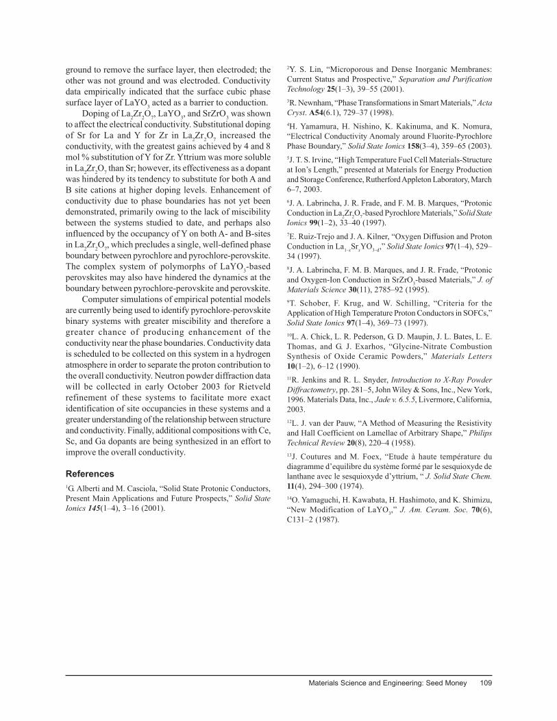
Materials Science and Engineering: Seed Money 109
ground to remove the surface layer, then electroded; theother was not ground and was electroded. Conductivitydata empirically indicated that the surface cubic phasesurface layer of LaYO3 acted as a barrier to conduction.
Doping of La2Zr2O7, LaYO3, and SrZrO3 was shownto affect the electrical conductivity. Substitutional dopingof Sr for La and Y for Zr in La2Zr2O7 increased theconductivity, with the greatest gains achieved by 4 and 8mol % substitution of Y for Zr. Yttrium was more solublein La2Zr2O7 than Sr; however, its effectiveness as a dopantwas hindered by its tendency to substitute for both A andB site cations at higher doping levels. Enhancement ofconductivity due to phase boundaries has not yet beendemonstrated, primarily owing to the lack of miscibilitybetween the systems studied to date, and perhaps alsoinfluenced by the occupancy of Y on both A- and B-sitesin La2Zr2O7, which precludes a single, well-defined phaseboundary between pyrochlore and pyrochlore-perovskite.The complex system of polymorphs of LaYO3-basedperovskites may also have hindered the dynamics at theboundary between pyrochlore-perovskite and perovskite.
Computer simulations of empirical potential modelsare currently being used to identify pyrochlore-perovskitebinary systems with greater miscibility and therefore agreater chance of producing enhancement of theconductivity near the phase boundaries. Conductivity datais scheduled to be collected on this system in a hydrogenatmosphere in order to separate the proton contribution tothe overall conductivity. Neutron powder diffraction datawill be collected in early October 2003 for Rietveldrefinement of these systems to facilitate more exactidentification of site occupancies in these systems and agreater understanding of the relationship between structureand conductivity. Finally, additional compositions with Ce,Sc, and Ga dopants are being synthesized in an effort toimprove the overall conductivity.
References1G. Alberti and M. Casciola, “Solid State Protonic Conductors,Present Main Applications and Future Prospects,” Solid StateIonics 145(1–4), 3–16 (2001).
2Y. S. Lin, “Microporous and Dense Inorganic Membranes:Current Status and Prospective,” Separation and PurificationTechnology 25(1–3), 39–55 (2001).3R. Newnham, “Phase Transformations in Smart Materials,” ActaCryst. A54(6.1), 729–37 (1998).4H. Yamamura, H. Nishino, K. Kakinuma, and K. Nomura,“Electrical Conductivity Anomaly around Fluorite-PyrochlorePhase Boundary,” Solid State Ionics 158(3–4), 359–65 (2003).5J. T. S. Irvine, “High Temperature Fuel Cell Materials-Structureat Ion’s Length,” presented at Materials for Energy Productionand Storage Conference, Rutherford Appleton Laboratory, March6–7, 2003.6J. A. Labrincha, J. R. Frade, and F. M. B. Marques, “ProtonicConduction in La2Zr2O7-based Pyrochlore Materials,” Solid StateIonics 99(1–2), 33–40 (1997).7E. Ruiz-Trejo and J. A. Kilner, “Oxygen Diffusion and ProtonConduction in La1–xSrxYO3–d,” Solid State Ionics 97(1–4), 529–34 (1997).8J. A. Labrincha, F. M. B. Marques, and J. R. Frade, “Protonicand Oxygen-Ion Conduction in SrZrO3-based Materials,” J. ofMaterials Science 30(11), 2785–92 (1995).9T. Schober, F. Krug, and W. Schilling, “Criteria for theApplication of High Temperature Proton Conductors in SOFCs,”Solid State Ionics 97(1–4), 369–73 (1997).10L. A. Chick, L. R. Pederson, G. D. Maupin, J. L. Bates, L. E.Thomas, and G. J. Exarhos, “Glycine-Nitrate CombustionSynthesis of Oxide Ceramic Powders,” Materials Letters10(1–2), 6–12 (1990).11R. Jenkins and R. L. Snyder, Introduction to X-Ray PowderDiffractometry, pp. 281–5, John Wiley & Sons, Inc., New York,1996. Materials Data, Inc., Jade v. 6.5.5, Livermore, California,2003.12L. J. van der Pauw, “A Method of Measuring the Resistivityand Hall Coefficient on Lamellae of Arbitrary Shape,” PhilipsTechnical Review 20(8), 220–4 (1958).13J. Coutures and M. Foex, “Etude à haute température dudiagramme d’equilibre du système formé par le sesquioxyde delanthane avec le sesquioxyde d’yttrium, “ J. Solid State Chem.11(4), 294–300 (1974).14O. Yamaguchi, H. Kawabata, H. Hashimoto, and K. Shimizu,“New Modification of LaYO3,” J. Am. Ceram. Soc. 70(6),C131–2 (1987).
110 FY 2003 ORNL Laboratory Directed Research and Development Annual Report
Progress Report Project Number: 3210-2074
Selective Area Chemical Vapor Deposition of Carbon Nanotube FilmsUsing Seeded Molecular Beams
G. EresCondensed Matter Sciences Division
Because carbon nanotubes (CNTs) are not a stable form of carbon, synthetic routes for formationof CNTs must be kinetically controlled. The objective of this project is to explore beams of smallcarbon-containing molecules for catalytic growth of CNTs. The molecular beam environment allowsreaction control at the single collision level, revealing the molecular parameters that influence thecatalytically induced conversion of hydrocarbons into CNTs. The key benefits of this approach includereducing the growth temperature of CNTs, controlling the structure (single wall vs multiwall) ofCNTs, increasing the yield, and circumventing formation of undesirable side products such asnanoparticles and amorphous carbon.
The main obstacle to widespread practical applicationof CNTs is the lack of controllable synthesis methods.Currently single-wall CNT (SW-CNT) synthesis isperformed either by evaporation and spontaneouscondensation of carbon or by high-temperature chemicalvapor deposition of hydrocarbons using transition metalcatalysts. The extreme reaction conditions in these growthtechniques induce a large number of secondary reactionsthat, in addition to SW-CNTs, produce numerousundesirable side products such as encapsulatednanoparticles and amorphous carbon. These side productsinterfere with applications, and must be removed beforethe CNTs can be used.
The molecular beams are generated by mixing smallamounts of hydrocarbon source gases (2%) with an inertcarrier gas such as He. The beam of carbon molecules isdirected at a heated substrate containing a thin film oftransition metal catalyst. Upon collision with the substrate,the carbon molecules either stick to the surface or bounceoff unchanged and are pumped away. For a fixed catalystcomposition, the outcome of the collision depends on thenature of the carbon-containing molecule, the incidentvelocity of the molecule, the incident angle of the molecule,and the substrate temperature. Each of these reactionparameters can be independently controlled to form thedesired reaction products, namely, pure SW-CNTs. Thefollowing results have been achieved during the first halfof the funding period in this project.
The key accomplishment of this project is the growthof SW-CNTs from molecular beams. There are no previousreports in the literature of SW-CNT growth from molecularbeams. The substrate temperature for SW-CNT growth
was in the range from 530°C to 680°C. Interestingly, CNTgrowth ceases above 680°C, suggesting that themechanism for CNT growth is governed by a surface-limited reaction. Compare these growth temperatures withtypical CNT growth temperatures by hot-wall CVD of900°C or higher.
The molecular structure was found to play animportant role in determining the CNT yield fromhydrocarbons. No SW-CNT growth was observed fromCH4, and only a small amount of SW-CNTs was foundwith C2H4. The best precursor for SW-CNT growth wasC2H2. The order CH4, C2H4, C2H2 represents a chain ofstable intermediates in carbon formation by thermaldecomposition of methane. This trend implies that themolecule that is the closest stable intermediate to carbonformation should be chosen to obtain the highest CNTyield.
Several transition metal catalyst were explored in theform of thin films, and chemically synthesized catalystnanoparticles, deposited on various substrates includingSi, sapphire, and quartz. The most effective catalyst wasFe, followed by Co. Surprisingly no CNT growth wasobserved with Ni. The composition and the thickness ofthe catalyst films also affected SW-CNT growth. No CNTgrowth was observed using chemically synthesizednanoparticles of Fe, Co, FeMo, and FePt.
In the second half of this project, work will be focusedon the chemical reaction dynamics of the most efficientcatalyst-carbon source molecule system. The goal is touse the molecular reaction parameters to tailor theproperties of as-grown SW-CNTs in application-relevantconfigurations.
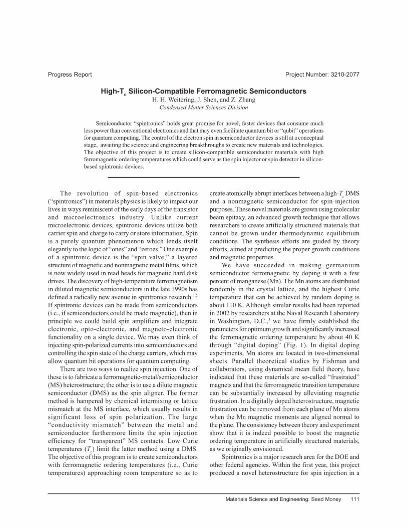
Materials Science and Engineering: Seed Money 111
Progress Report Project Number: 3210-2077
High-Tc Silicon-Compatible Ferromagnetic SemiconductorsH. H. Weitering, J. Shen, and Z. Zhang
Condensed Matter Sciences Division
Semiconductor “spintronics” holds great promise for novel, faster devices that consume muchless power than conventional electronics and that may even facilitate quantum bit or “qubit” operationsfor quantum computing. The control of the electron spin in semiconductor devices is still at a conceptualstage, awaiting the science and engineering breakthroughs to create new materials and technologies.The objective of this project is to create silicon-compatible semiconductor materials with highferromagnetic ordering temperatures which could serve as the spin injector or spin detector in silicon-based spintronic devices.
The revolution of spin-based electronics(“spintronics”) in materials physics is likely to impact ourlives in ways reminiscent of the early days of the transistorand microelectronics industry. Unlike currentmicroelectronic devices, spintronic devices utilize bothcarrier spin and charge to carry or store information. Spinis a purely quantum phenomenon which lends itselfelegantly to the logic of “ones” and “zeroes.” One exampleof a spintronic device is the “spin valve,” a layeredstructure of magnetic and nonmagnetic metal films, whichis now widely used in read heads for magnetic hard diskdrives. The discovery of high-temperature ferromagnetismin diluted magnetic semiconductors in the late 1990s hasdefined a radically new avenue in spintronics research.1,2
If spintronic devices can be made from semiconductors(i.e., if semiconductors could be made magnetic), then inprinciple we could build spin amplifiers and integrateelectronic, opto-electronic, and magneto-electronicfunctionality on a single device. We may even think ofinjecting spin-polarized currents into semiconductors andcontrolling the spin state of the charge carriers, which mayallow quantum bit operations for quantum computing.
There are two ways to realize spin injection. One ofthese is to fabricate a ferromagnetic-metal/semiconductor(MS) heterostructure; the other is to use a dilute magneticsemiconductor (DMS) as the spin aligner. The formermethod is hampered by chemical intermixing or latticemismatch at the MS interface, which usually results insignificant loss of spin polarization. The large“conductivity mismatch” between the metal andsemiconductor furthermore limits the spin injectionefficiency for “transparent” MS contacts. Low Curietemperatures (Tc) limit the latter method using a DMS.The objective of this program is to create semiconductorswith ferromagnetic ordering temperatures (i.e., Curietemperatures) approaching room temperature so as to
create atomically abrupt interfaces between a high-Tc DMSand a nonmagnetic semiconductor for spin-injectionpurposes. These novel materials are grown using molecularbeam epitaxy, an advanced growth technique that allowsresearchers to create artificially structured materials thatcannot be grown under thermodynamic equilibriumconditions. The synthesis efforts are guided by theoryefforts, aimed at predicting the proper growth conditionsand magnetic properties.
We have succeeded in making germaniumsemiconductor ferromagnetic by doping it with a fewpercent of manganese (Mn). The Mn atoms are distributedrandomly in the crystal lattice, and the highest Curietemperature that can be achieved by random doping isabout 110 K. Although similar results had been reportedin 2002 by researchers at the Naval Research Laboratoryin Washington, D.C.,3 we have firmly established theparameters for optimum growth and significantly increasedthe ferromagnetic ordering temperature by about 40 Kthrough “digital doping” (Fig. 1). In digital dopingexperiments, Mn atoms are located in two-dimensionalsheets. Parallel theoretical studies by Fishman andcollaborators, using dynamical mean field theory, haveindicated that these materials are so-called “frustrated”magnets and that the ferromagnetic transition temperaturecan be substantially increased by alleviating magneticfrustration. In a digitally doped heterostructure, magneticfrustration can be removed from each plane of Mn atomswhen the Mn magnetic moments are aligned normal tothe plane. The consistency between theory and experimentshow that it is indeed possible to boost the magneticordering temperature in artificially structured materials,as we originally envisioned.
Spintronics is a major research area for the DOE andother federal agencies. Within the first year, this projectproduced a novel heterostructure for spin injection in a
112 FY 2003 ORNL Laboratory Directed Research and Development Annual Report
Fig. 1. Magnetization of a “random” and a “digital” manganese-germanium heterostructure as a function of temperature. Digital dopingsignificantly enhances ferromagnetism.
silicon compatible geometry and produced a powerfulstrategy toward enhancing the ferromagnetic orderingtemperature in a dilute magnetic semiconductor. Theseaccomplishments represent major contributions towardsolving the bottleneck issues for spintronics research andtechnology.
References1S. A. Wolf, D. D. Awschalom, R. A. Buhrman, J. M. Daughton,S. von Molnár, M. L. Roukes, A. Y. Chtchelkanova, and D. M.Treger, “Spintronics, A Spin-Based Electronics Vision for theFuture,” Science 294, 1488 (2001).2T. Dietl, “Ferromagnetic Semiconductors,” Semicond. Sci.Technol. 17, 377 (2002)3Y. D. Park, A. T. Hanbicki, S. C. Erwin, C. S. Hellberg, J. M.Sullivan, J. E. Mattson, T. F. Ambrose, A. Wilson, G. Spanos,and B. T. Jonker, “A Group-IV Ferromagnetic Semiconductor:MnxGe1–x,” Science 295, 651 (2002).
Materials Science and Engineering: Seed Money 113
Progress Report Project Number: 3210-2081
An Innovative Technique for Bimaterial Interface Toughness ResearchJ. A. Wang,1 K. C. Liu,2 I. G. Wright,2 and L. R. Xu3
1Nuclear Science and Technology Division2Metals and Ceramics Division
3Vanderbilt University
In general, the weakest link in bimaterials occurs at the interface between dissimilar materials,such as the interface between a thin film and its substrate. In order to make multilayered electronicdevices or structural composites with a long-term reliability, the fracture behavior of these interfacesmust be known. Unfortunately, none of the state-of-the-art testing methods for evaluating interfacefracture toughness fully conform to fracture mechanics theory, as is evident in existing data that showsevere scatter and procedure dependence in thin-film evaluation methods. This project addresses theproblems associated with this deficiency and offers an innovative testing procedure for determinationof interface fracture toughness applicable to thin-coating materials in general.
The drive toward increased performance, efficiency,and reduced environmental pollution in heat engines,energy conversion processes, and many chemicalprocesses involves operation of equipment at highertemperatures, often in increasingly corrosiveenvironments. All materials of construction requireenvironmental protection, and in high-temperatureenvironments, the ability of the protective barrier to remainadherent to the surfaces is critical. As a result, measurementof the toughness of the substrate-barrier interfaceaddressed in this project is expected to enhance the abilityto improve the performance of many of the componentsneeded in, for example, the DOE’s Vision 21 anddistributed generation programs, as well as in DODprograms to improve liners for combustors and thermalbarrier coatings for gas turbine engines, and to developbetter thermal protection systems for space vehicles.
An innovative technology for measuring interfacetoughness will be demonstrated for oxide scales formedon high-temperature alloys. This new approach includesthe development of analytical and experimental proceduresand associated bimaterial fracture mechanics theory forevaluating interface fracture toughness. The expectedoutcomes are (1) improved life prediction capability forhigh-temperature environmental and thermal barriercoatings, (2) understanding of the mechanism of theinterface crack initiation, and (3) determination ofunambiguous values for interface fracture toughness. Thisinnovative technique is expected to greatly assist thedevelopment of coating materials with improved protectivecapabilities and provide a reliable method for use inassessing material performance.
In the Phase I of the proposed project, the followingprogress was made as scheduled:• Upgraded biaxial test machine with a new load cell
capable of high resolution required for torsionaltesting on thin film materials.
• Selected a Ni-based super alloy (MA956) currentlyused in high-temperature heat exchangers as the basematerial on which a thin coating will be formed byoxidation. Two types of notch configurations, a V-shape and a U-shape with different aspect ratios, wereused in the new spiral notch torsion test (SNTT)specimens. The specimens are currently beingfabricated at a local machine shop.
• To enhance the latitude of this project, a collaborationwas discussed with Dr. Matt Ferber of the ceramicstructure group at the High Temperature MaterialsLaboratory (HTML) for using his thermal-barrier-coating (TBC) material in the proposed study. Thespecimen design appropriate for this material was alsocompleted.
• Developed a fatigue precrack procedure, whichutilizes underpeak detector to detect and controlfatigue crack growth.
• Developed the finite element models for the SNTTspecimens with specified notch configurations andthe boundary conditions.
The great technical challenges are expected to be metboth in developing experimental procedures and testingapparatus, and theoretical and analytical evaluation ofinterface toughness for the proposed configurations, whichwill be carried out in the Phase II research in FY 2004.

114 FY 2003 ORNL Laboratory Directed Research and Development Annual Report
The development of this innovative testing procedure willsupport innovation in the development and use of materialsand coatings by providing reliable methods for industryto use in assessing their performance and provide industrywith the means to develop and use better (more advanced)
materials and coatings through a better understanding ofhow they behave in practical situations. Knowledge of howthe toughness of coating-substrate interfaces is influencedby alloy and coating parameters will greatly aid improvedenvironmental/thermal barrier design.
Materials Science and Engineering: Seed Money 115
Progress Report Project Number: 3210-2083
Nanoporous Inorganic Membranes for High Selectivity Hydrogen SeparationsL. K. Mansur and B. L. Bischoff
Metals and Ceramics Division
The United States is committed to a future hydrogen economy. Hydrogen is not generally availableas an elemental resource. It can be dissociated from compounds, such as from hydrocarbons or water,by high-temperature chemical reactions. Subsequent to dissociation, effective recovery of hydrogenfrom gas mixtures becomes a central issue. We are addressing this issue by research on the nanoscienceof inorganic gas separation membranes. Pore sizes in commercially available membranes range fromabout 4 nm to many micrometers. Knudsen diffusion, surface transport, and other reasonably well-understood permeation processes provide limited gas selectivity in such commercial membranes.Recently, we have fabricated experimental inorganic membranes with pore sizes of 1 nm or less.Proof-of-principle experiments are now being carried out on these membranes with the goal ofdemonstrating exceptionally high selectivity for hydrogen with respect to a number of other gasesincluding a hydrocarbon and carbon dioxide. Guided by theoretical models, we are analyzing thesedata for evidence of the dominant separation mechanisms in operation and, in particular, for thermallyactivated atomic-level separation mechanisms.
Approximately 40 nanoporous membranes have beenfabricated and characterized over the past 2 years in earlierresearch. Much of the permeation work to characterizethe selectivity of these membranes employed helium andsulfur hexafluoride (SF6) up to temperatures of 275°C.This base of historical data was examined at the outset ofthe present research effort.
Since hydrogen separation from hydrocarbonmixtures is the focus of our research, H2 was added to themembrane evaluation protocol and propane (C3H8) waschosen to replace SF6. A modification to the test systemwas completed for these flammable gases. The requiredsafety documentation was completed and approved. Thesystem is now fully operational for analysis of thepermeation of individual gases, including H2, He, CO2,and C3H8 up to 275°C. Measurements with SF6 will alsobe carried out for comparison with earlier work. In orderto help determine the fundamental operating mechanismsof gas separation, it is essential that data be obtained overa wider range of temperatures. Therefore, more recently,a second system has been modified to measure thepermeation of individual gases up to approximately 400°C.In addition, this second system gives us the capability tomeasure the separation of hydrogen from mixtures ofgases. During the past month, permeation measurementswere initiated. Nanoporous membranes are currently beingevaluated with the series of gases mentioned. In severalcases the preliminary data show selectivities higher thanthat for Knudsen diffusion, indicating that the membranepore size is indeed in the desired nanometer-size regime.
In order to most effectively analyze the experimentaldata being accumulated, the dominant operatingmechanisms of membrane transport need to be known. Tothis end we have distilled parametric dependencies of keymechanisms of gas transport into simple and readilyapplicable expressions. Key parameters includetemperature T, pressure P, molecular mass m, kineticmolecular diameter dm, pore diameter dp, molecularcollision mean free path λ, and several thermal activationenergies. The latter are Ha, the heat of gas adsorption, Es,the activation energy for surface diffusion, and Ed, theactivation energy for nanopore diffusion.
The most important characteristic of membranes thatdictates the dominant transport mechanism is the porediameter or, more precisely, the ratio of the pore diameterto two important physical characteristics of the gas, λ anddm. Most gases of interest have kinetic diameters betweenone-fourth and two-thirds of a nanometer. Generally, forpore diameters >2 nm, the important permeationmechanisms in operation are Knudsen diffusion andsurface transport, together with molecular diffusion andviscous flow (Poiseuille or laminar flow) at larger porediameters. For pore diameters of about 1 nm and smaller,other mechanisms, which are covered by the term“nanopore diffusion,” come into operation. Severalmechanisms of gas transport through a membrane aresummarized in Table 1. Expressions for selectivity andpermeance also are given in the table for those cases wherethe dependencies on important variables can be expressedin simple form without extensive qualifying statements orlimiting conditions.
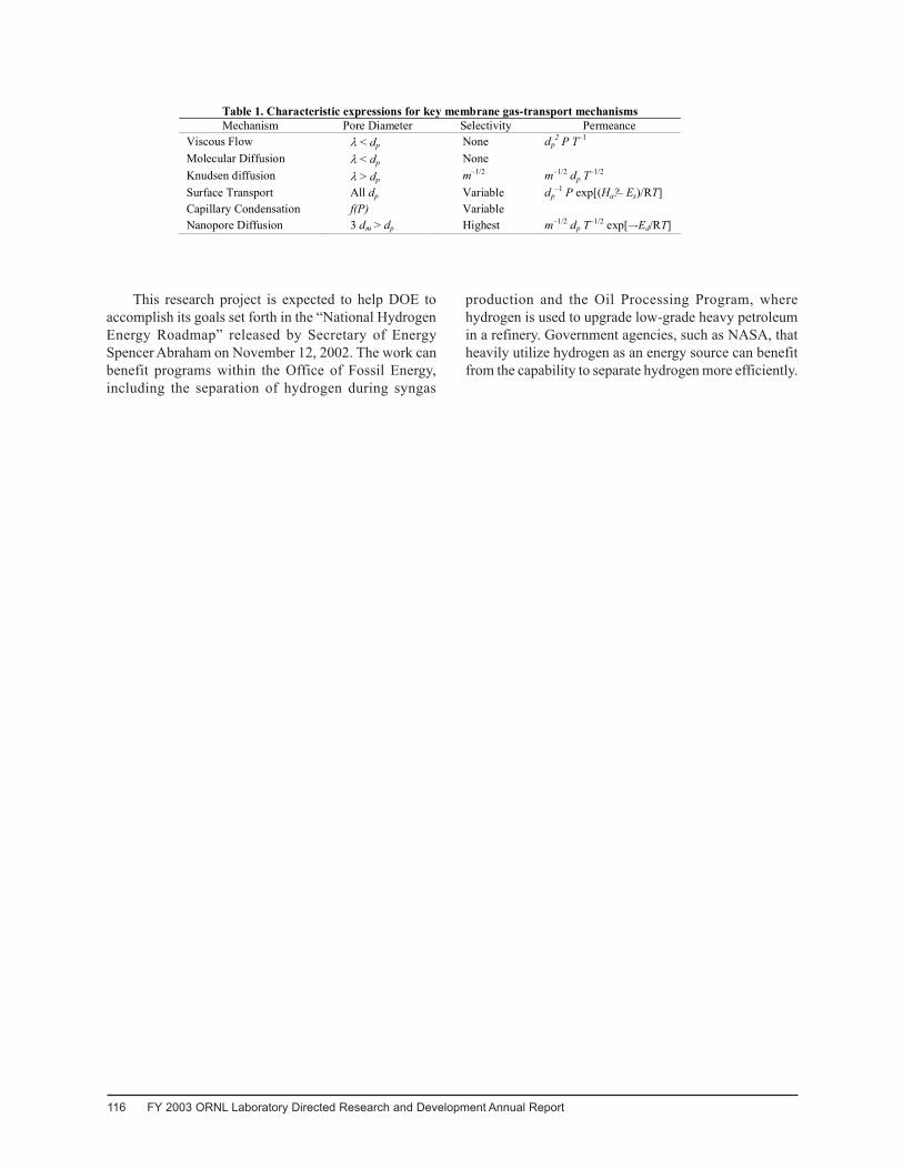
116 FY 2003 ORNL Laboratory Directed Research and Development Annual Report
This research project is expected to help DOE toaccomplish its goals set forth in the “National HydrogenEnergy Roadmap” released by Secretary of EnergySpencer Abraham on November 12, 2002. The work canbenefit programs within the Office of Fossil Energy,including the separation of hydrogen during syngas
production and the Oil Processing Program, wherehydrogen is used to upgrade low-grade heavy petroleumin a refinery. Government agencies, such as NASA, thatheavily utilize hydrogen as an energy source can benefitfrom the capability to separate hydrogen more efficiently.
Table 1. Characteristic expressions for key membrane gas-transport mechanisms Mechanism Pore Diameter Selectivity Permeance
Viscous Flow λ < dp None dp2 P T–1
Molecular Diffusion λ < dp None Knudsen diffusion λ > dp m–1/2 m–1/2 dp T–1/2 Surface Transport All dp Variable dp
–1 P exp[(Ha? – Es)/RT] Capillary Condensation f(P) Variable Nanopore Diffusion 3 dm > dp Highest m–1/2 dp T–1/2 exp[–-Ed/RT]
Materials Science and Engineering: Seed Money 117
Progress Report Project number: 3210-2084
High-Aspect-Ratio Carbon Nanofiber Probes for Scanning Probe MicroscopyM. L. Simpson,1 M. A. Guillorn,1 C. Rouleau,2 D. Hensley,1,2
R. J. Kasica,1 M. J. Doktycz,3 and A. V. Melechko1,4
1Engineering Science and Technology Division2Condensed Matter Sciences Division
3Life Sciences Division4University of Tennessee
The objective of this project is to develop the first technique for the synthesis of high-resolution,high-aspect-ratio scanning-probe-microscope (SPM) tips that can be implemented in a large-scalefabrication process. This technique will be based on the ORNL-developed vertically aligned carbonnanofibers (VACNF) technology. While other methods currently exist for the production of this typeof probe tip, the use of the VACNF will surpass these techniques since VACNFs can be synthesizedcompletely deterministically in a wafer-scale fabrication process. This allows for thousands of identicaltips to be fabricated simultaneously in precise locations with total control over their morphology.
Scanning probe microscopy (SPM) has become anindispensable tool for the analysis of surfaces and theexploration of general substrate morphology at thenanoscale and microscale. Moreover, SPM techniqueshave been used to investigate a wide variety of materialproperties beyond substrate topography. The range ofapplications spans a vast array of scientific disciplinesranging from solid state physics to biology, environmentalscience to polymer engineering. The currently usedmethods for producing high-resolution, high-aspect-ratiotips for SPM applications are based on processes serial innature; that is, only a single tip can be fabricated at a time.The goal of this project is to integrate synthesis of verticallyaligned carbon nanofibers (VACNFs) with standardcantilever fabrication processes and to characterize thehigh-aspect-ratio VACNF SPM tips obtained in suchmethod.
We have demonstrated that VACNFs can besynthesized in a completely deterministic manner using acatalytic dc, plasma-enhanced, chemical vapor depositionprocess. Features such as the location, length, tip diameter,shape, and chemical composition of VACNFs can beprecisely controlled during the synthesis process.Functional microfabricated device structures have beenfabricated that exploit both the electrical and mechanicalproperties of single and multiple VACNF. These structureshave been fabricated on a variety of substrates includingwhole 10-cm-diameter Si, Si-on-insulator (SOI) and quartzwafers. This material meets the required specifications for
high-aspect-ratio SPM tips. In addition, it offers a numberof other features that may allow it to surpass all othermaterials presently used in SPM tip manufacturing.
The fabrication process for microcantilevers withVACNF tips have been developed during FY 2003.Individual processing steps compatible with handlingmicrosctructures with high-aspect-ratio features such asVACNFs have been developed and tested. The first batchof cantilevers with VACNF tips has been obtained, thusproving the feasibility of the idea. Figure 1 shows an SEMimage of a finished device. The sharpness of the VACNFtips has been improved via changes in the catalystpreparation process. The diameter of the nanofibercoincides with the diameter of the catalyst particle. Wehave found the techniques to prepare smaller nanoparticlesthat can be prepared using standard photolithography, thusmaking the complete fabrication an inexpensive and high-throughput method.
The devices obtained after optimization of allprocessing steps will be characterized, and theirperformance will be compared to currently availableatomic force microscope tips in application areas that arecritical to DOE and NIH. Micro- and nano-fabricatedstructures and complex biological systems, two majorresearch thrust areas at ORNL, possess a varied surfacetopography that is often best characterized by SPMtechniques. However, they can only be imaged accuratelywith high-resolution high-aspect-ratio tips. We will explorethe application of the VACNF probe tips in these two targetareas as they show significant promise to benefit programsat ORNL.
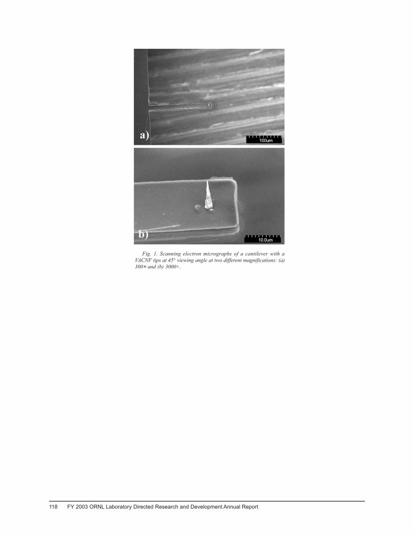
118 FY 2003 ORNL Laboratory Directed Research and Development Annual Report
Fig. 1. Scanning electron micrographs of a cantilever with aVACNF tips at 45° viewing angle at two different magnifications: (a)300× and (b) 3000×.
Materials Science and Engineering: Seed Money 119
Progress Report Project Number: 3210-2087
In Situ Studies of Hydrogen Storage Materials Using Neutron ScatteringC. J. Rawn,1,2 J. Y. Howe,1 B. C. Chakoumakos,3 J. L. Robertson,3 and F. C. Montgomery1
1Metals and Ceramics Division, Oak Ridge National Laboratory2Materials Science and Engineering Department, University of Tennessee
3Condensed Matter Sciences Division, Oak Ridge National Laboratory
This project concentrates on using in situ neutron diffraction studies to answer structural andthermodynamic issues about the role of hydrogen in hydrogen containing compounds. The first tasksunderway are collaborating with personnel from the neutron scattering facility at Chalk River tocollect neutron diffraction data at ambient conditions on candidate hydrogen storage materials and todesign and construct a new pressure cell for use at different temperature and pressure ranges of interestfor the investigation of suitable hydrogen storage materials. Future research includes proof-of-principleexperiments using the new pressure cell to demonstrate its utility for implementation of neutronscattering experiments on hydrogen-containing compounds.
Progress ReportTo obtain a pressure cell for use at different
temperature/pressure ranges of interest for theinvestigation of suitable hydrogen storage materials. Toverify the efficacy of the cell by studying NaAlD4 anddemonstrate that we can generate details surrounding therole of H atoms in the atomic structure.
To collect neutron powder diffraction data on thecandidate hydrogen storage materials NaAlD4 doped withthe addition of TiCl3 as a catalyst. With high-qualityneutron powder diffraction data we can use the Rietveldmethod to determine the positions of Ti in the crystalstructure. Additional in situ experiments have beenproposed to observe hydrogen absorption and desorptionunder service conditions of hydrogen storage materials.From these experiments we hope to understand the paththat the hydrogen atoms take during absorption anddesorption and to evaluate a high-temperature/high-pressure cell, designed by the group at Chalk River, forpossible procurement and use at the High Flux IsotopeReactor.
Our two-phase proposal to obtain beamtime on thepowder diffractometer at the Chalk River neutronscattering facility has been review and approved, and weare hoping to start data collection in early March. Thefirst experiments we wish to conduct are at ambienttemperature and ambient pressure on NaAlD4 with andwithout the addition of TiCl3 as a catalyst. There are severalexplanations in the literature for where the Ti must belocated within in the crystal structure; however, to datethis has not been shown experimentally using neutronscattering techniques. Our intent is to collect a high-qualityneutron powder diffraction pattern and examine the data
using the Rietveld method to determine the sites occupiedby Ti in the NaAlD4 unit cell. A third data set is to becollected on NaAlD4 + TiCl3 desorbed to Na3AlD6 +products. We are collaborating with Joachim Schneibel(Metals and Ceramics Division) to synthesize NaAlD4 withTiCl3 from as-received NaAlH4 by desorbing the materialand recharging it with D2 gas.
One of the main goals of this proposal is obtain ahigh-pressure/high-temperature cell to study hydrogenstorage materials with in situ neutron powder diffractiontechniques. To this end we are collaborating with LachlanM.D. Cranswich, a Research Council Officer from theNeutron Program for Materials Research at Chalk RiverLaboratories (Chalk River, Ontario, Canada). In July welearned from Mr. Cranswick that the Chalk River groupwas in the first stages of designing such a cell, and inOctober Mr. Cranswich visited ORNL and discussed theearly stages of a high-pressure/high-temperature celldesign. Figure 1 shows the mass flow control layoutdesigned to minimize the amount of tubing. The design ofthis pressure cell is such that it will work in conjunctionwith a commercial Cryofurnace, which we currently haveavailable at the High Flux Isotope Reactor (HFIR), forchanging the temperature. For the current cell design, thehighest obtainable pressure would be 10 bar, and we haveproposed modifications to the design to obtain pressuresof 50 bar. For this increased pressure range, several factorssuch as the choice of container material and the additionof an external gas booster are being considered. We havereceived two of mock-up sample holders that are the sizesand geometry used on the powder diffraction beamline atthe Chalk River facilities. These cells contain porous metalfilters that will allow the gas into the sample holders
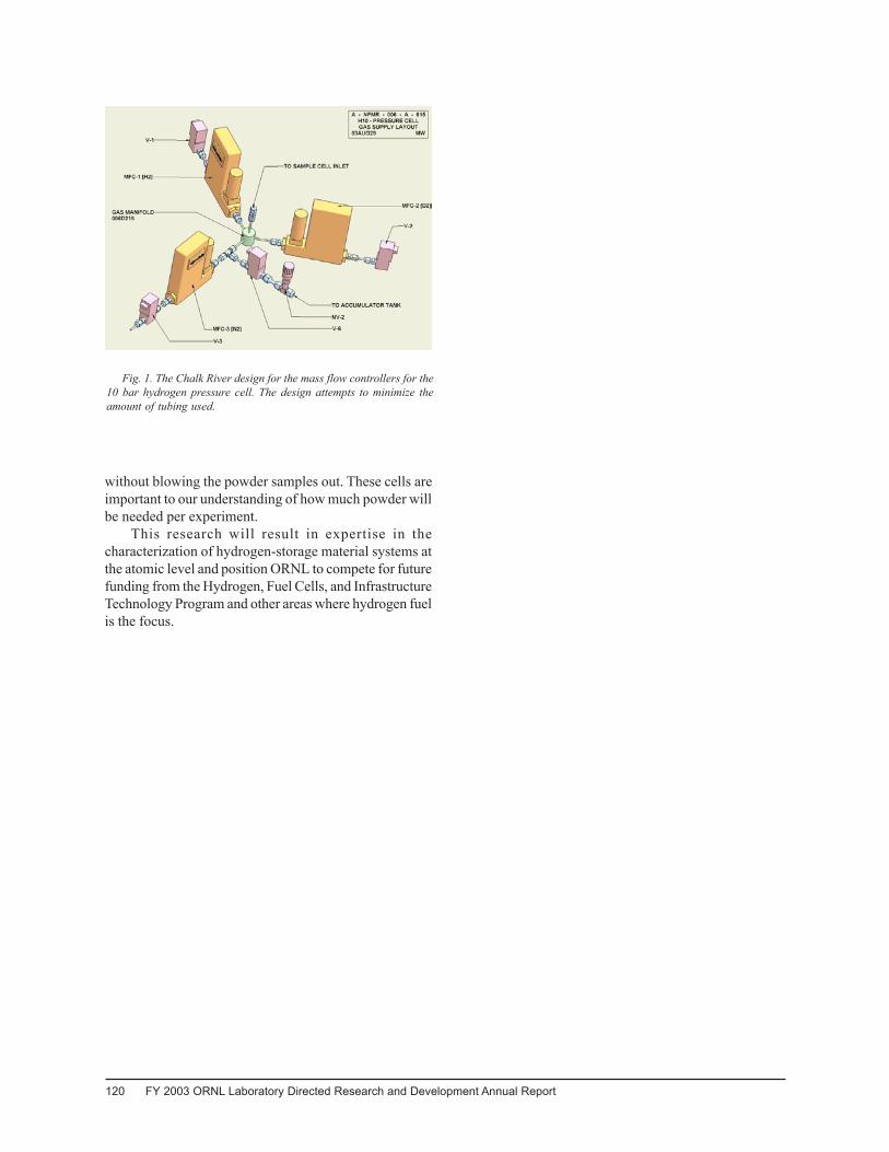
120 FY 2003 ORNL Laboratory Directed Research and Development Annual Report
Fig. 1. The Chalk River design for the mass flow controllers for the10 bar hydrogen pressure cell. The design attempts to minimize theamount of tubing used.
without blowing the powder samples out. These cells areimportant to our understanding of how much powder willbe needed per experiment.
This research will result in expertise in thecharacterization of hydrogen-storage material systems atthe atomic level and position ORNL to compete for futurefunding from the Hydrogen, Fuel Cells, and InfrastructureTechnology Program and other areas where hydrogen fuelis the focus.
Materials Science and Engineering: Seed Money 121
Progress Report Project Number: 3210-2093
Alanates for High-Capacity Hydrogen StorageJ. H. Schneibel,1 D. S. Easton,2 S. Babu,1 and S. A. Speakman1
1Metals and Ceramics Division2Consultant, Metals and Ceramics Division
We propose to investigate the hydrogen absorption/desorption properties of alanate compounds[NaAlH4, LiAlH4, AlH3, Mg(AlH4)2] capable of storing up to approximately 10 wt % hydrogen. Thesynthesis of these materials will be accompanied and guided by thermodynamic modeling and crystalstructure analysis. Alloying will be carried out by high-energy milling. Elements or compounds willbe added to improve the absorption/desorption kinetics and to shift the absorption/desorption conditionscloser to ambient conditions.
To reduce the country’s dependence on foreign oilsupplies and to promote a cleaner environment, thePresident has proposed the FreedomCar (FreedomCooperative Automotive Research) initiative. Its long-termgoal is to develop technologies for hydrogen-powered fuelcell cars and trucks. This project focuses on a particularlyimportant issue of the initiative, namely, hydrogen storage.The objective is to develop materials which can absorband desorb large amounts of hydrogen (e.g., 10 wt %) atnear-ambient conditions.
Alanate materials (i.e., materials containing AlH4–
ions, such as for example LiAlH4) will be prepared byhigh-energy ball milling of powder precursor materials.Small quantities of elements or compounds with catalyticactivity will be added to improve the absorption/desorptionkinetics (“micro-alloying”). Macro-alloying (i.e., ≈1 wt %and above) with the aim of shifting the absorption/desorption conditions closer to ambient will be guided bythermodynamic calculations as well as electronegativityand atomic size considerations.
During FY 2003, this project focused on experimentsdesigned to assure that we are able to reproduce existingresults for high-performance hydrogen-storage materialsand that our equipment for measuring hydrogen storagecapacity values is performing properly. Considerable effortwas spent on determining the precision and reproducibilityof a recently acquired piece of equipment forcharacterizing hydrogen-storage materials. This equipmentmeasures the hydrogen pressure as a function of thehydrogen concentration in the material, for absorption anddesorption at preselected temperatures (the so-calledpressure-composition-isotherm, PCI). The equipment alsomeasures, as a function of temperature and pressure, therates with which hydrogen is absorbed and desorbed.Following published information, commercially availablesodium alanate, NaAlH4, was high-energy milled with
2 wt % of TiCl3. Its hydrogen absorption and desorptionbehavior was measured as a function of pressure. Thecurves obtained demonstrated the two-stagedecomposition reaction:
3NaAlH4 → Na3AlH6 + 2Al + 3H2 → 3NaH + 3Al + 5/2 H2 (1)
According to a desorption PCI curve measured byus, the hydrogen storage capacity was 4.95 wt %. Thehydrogen storage capacity was independently measuredby weighing the fully charged as well as the materialdischarged according to the right-hand side of Eq. (1).The storage capacity measured in this way was 4.66 wt %,which is in reasonable agreement with the PCI value of4.95 wt %. These values are not as high as the theoreticalcapacity, 5.6 wt %, but are in agreement with typical valuesfound in the open literature. We have now reached thepoint at which we will be able to perform experimentswith novel compositions.
If improved hydrogen storage capacities can beobtained, and if absorption and desorption occur at close-to-ambient conditions, this project will be very valuablefor the Energy Efficiency and Renewable Energy (EERE)program of DOE.
Other federal agencies involved in supporting cuttingedge research in carbon nanotube synthesis and electronicapplication such as DARPA and NASA will directly benefitfrom increased control over the carbon nanotube filmgrowth process. A specific example is the application ofcarbon nanotubes as field emitters. The ability to controlthe growth rate and the growth temperature is also relevantto mass production of carbon nanotubes. Agencies thatare involved in supporting carbon nanotube compositeresearch such as NASA would directly benefit from a high-rate carbon nanotube synthesis process.
122 FY 2003 ORNL Laboratory Directed Research and Development Annual Report
Progress Report Project Number: 3210-2101
Enhancing Performance of Hydrogen Storage Materials through Nanoscale DesignV. K. Sikka,1 G. Muralidharan,1 T. J. Huxford,1 T. M. Besmann,1 N. C. Gallego,1 and M. P. Paranthaman2
1Metals and Ceramics Division2Chemical Sciences Division
Insufficient gravimetric capacities and slow hydriding/dehydriding kinetics have been recognizedas hurdles to be overcome in the quest for future hydrogen storage materials. The objective of thisproject is to examine a novel approach for enhancing the hydriding/dehydriding kinetics based on theuse of nanometer-thick films. The feasibility of this approach will be studied by depositing films ofmagnesium on the interior surfaces of a microporous silica gel with a large surface area (up to 1000 m2/g)and examining the hydriding/dehydriding characteristics of the resulting material. The use of silicagel as the template material is a key to obtaining improved kinetics without sacrificing storage capacity.Improved kinetics and lower operating temperatures are benefits anticipated as a result of using thisapproach.
Hydrogen-storage materials are of great interest forthe new national and international interest in the hydrogeneconomy. Based on the potential use of hydrogen storagematerials in automotive applications, a storage criteria of9 wt % of hydrogen has been set as a national goal andthere are many efforts under way to develop such materials.In addition to meeting the gravimetric capacity, suchmaterials should also be capable of adsorbing anddesorbing the hydrogen at temperatures less than 100°Cat pressures of 1–10 atm. A number of metal hydrides havebeen studied for their potential use as hydrogen-storagematerials. Such studies have shown that slow kinetics ofthe hydriding/dehydriding reaction, high temperaturesrequired to absorb/release the hydrogen, or insufficientstorage capacities limit the use of metal hydrides.
A number of approaches, such as physical andchemical treatments, have been carried out to improve thehydriding and dehydriding kinetics of metal hydrides withlimited success. Our approach to addressing this problemis based on developing a general scheme for improvingthe hydriding/dehydriding kinetics of all hydrogen storagematerials of interest. We plan to use magnesium as a modelmaterial for developing and demonstrating our concept.In addition to improving the hydriding/dehydridingkinetics using this methodology, our objective is to alsoachieve reduced operating temperatures in the range of100–150°C in such films.
The core theme of our approach is the use of thinfilms of hydrogen-storage materials with a thickness ofless than 50 nm. A significant benefit in using such filmsis that diffusion is required only over very short distanceswhen the surfaces of the thin films are exposed to the gas.In addition, to achieve sufficient gravimetric storagecapacity, the internal surfaces of a foam-like material with
a large surface area and an interconnected pore structurethat is permeable to the surrounding gas medium have tobe coated with the thin film that can store hydrogen. Anexample of this kind of a material is silica gel. These gelsare commonly used for humidity control, and catalystsupport. The combined use of the silica gel as a templateand a thin-film hydrogen-storage material is unique andnovel.
Significant progress has already been made over thefirst three months of the project. Several candidate silicagel materials have been identified and are currently beingevaluated for use in this work. The pore surface area hasbeen evaluated for one particular batch of materials usingBrunauer-Emmett-Teller gas adsorption measurements.The results show a typical total accessible pore surfacearea of about 430 m2/g. Experiments are under way toevaluate deposition techniques that would be suitable forcoating the internal surfaces of these gels with Mg/Mg-alloy composite thin films. Initial experiments haveexplored the use of physical vapor deposition methods tocoat the silica gels with magnesium. These techniquesexploit the fact that the vapor pressure of magnesium ishigh at relatively low temperatures due to its low meltingpoint. Silica gels were exposed to an atmosphere consistingof a high partial vapor pressure of magnesium throughheat treatment in a furnace either in a sealed quartz tubeor in a flowing Ar/H2 atmosphere. The resulting materialwas crushed and the phases present were analyzed throughX-ray diffraction. MgO peaks were observed in thediffraction pattern, indicating that magnesium was indeeddeposited but was subsequently oxidized during exposureto air. Future experiments will focus on protecting themagnesium films through handling in an inert atmosphereand subsequently depositing palladium to prevent

Materials Science and Engineering: Seed Money 123
oxidation. An alternate and novel technique using rapidsequential heating of magnesium and palladium with ahigh-power IR lamp in a flowing Ar/H2 atmosphere hasalso been attempted to minimize the problems due tooxidation of magnesium. Further characterization of thismaterial is in progress.
Chemical vapor infiltration will also be pursued asan alternative technique for depositing composite thinfilms. Experiments to evaluate the hydriding/dehydridingproperties of the material produced have also beeninitiated.
Hydrogen storage and delivery materials are ofsignificant interest to DOE and other federal agencies suchas DARPA. If this scheme is successful, engineeringhydrogen-storage materials based on magnesium withgravimetric capacities up to 9.3 wt % may be feasible,thus satisfying both the existing and future DOE criteria.There is also the additional advantage that, if necessary,this methodology can be applied to other hydrogen-storagematerials.


