COMPUTER ARCHITECTURE LABORATORY 01 CA Laboratory general objectives The laboratory exercises and homework are mandatory components of the CA course. The main objective of the laboratory exercises is the developing of synthesizable VHDL models of simple MIPS CPUs using the Xilinx ISE tools and Digilent Development Boards (DDB). The main laboratory themes are: • Design with Xilinx ISE tools and Digilent Development Boards (DDB). • Synthesizable VHDL hardware components implemented and tested on the DDB. • VHDL design of MIPS single cycle/multi-cycle/pipeline CPU implemented and tested on DDB. The associated homework helps to prepare the laboratory exercises and improve the specific problem solving ability of the students. Some extracts of recommended reading assignments are included in Laboratory materials, the original documents and VHDL examples are available on the web-site. 1
Transcript
COMPUTER ARCHITECTURE LABORATORY 01
CA Laboratory general objectives The laboratory exercises and homework are mandatory components of the CA course. The main objective of the laboratory exercises is the developing of synthesizable VHDL models of simple MIPS CPUs using the Xilinx ISE tools and Digilent Development Boards (DDB). The main laboratory themes are:
• Design with Xilinx ISE tools and Digilent Development Boards (DDB). • Synthesizable VHDL hardware components implemented and tested on the
DDB. • VHDL design of MIPS single cycle/multi-cycle/pipeline CPU implemented and
tested on DDB. The associated homework helps to prepare the laboratory exercises and improve the specific problem solving ability of the students. Some extracts of recommended reading assignments are included in Laboratory materials, the original documents and VHDL examples are available on the web-site.
1
COMPUTER ARCHITECTURE LABORATORY 01
Laboratory 01
Introduction to Software/Hardware development environment for VHDL based designs.
1. Objectives Familiarize the students with
• Xilinx ISE WebPack CAD tools – ISE Quick Start Tutorial • Xilinx® Synthesis Technology (XST) XST User Guide • Digilent Development Boards (DDB)
Digilent Basys Board – Reference Manual • Xilinx Spartan 3E FPGA family
2. Necessary resources (the kits are available and installed on
the workstations from the laboratory) Digilent Adept Software: download page
Digilent Basys Board:
• Reference Manual • Schematic
Xilinx ISE WebPACK is a part of the Xilinx Design Suite, ISE Design Suite – 14.7 Full Product Installation Xilinx ISE Software manual:
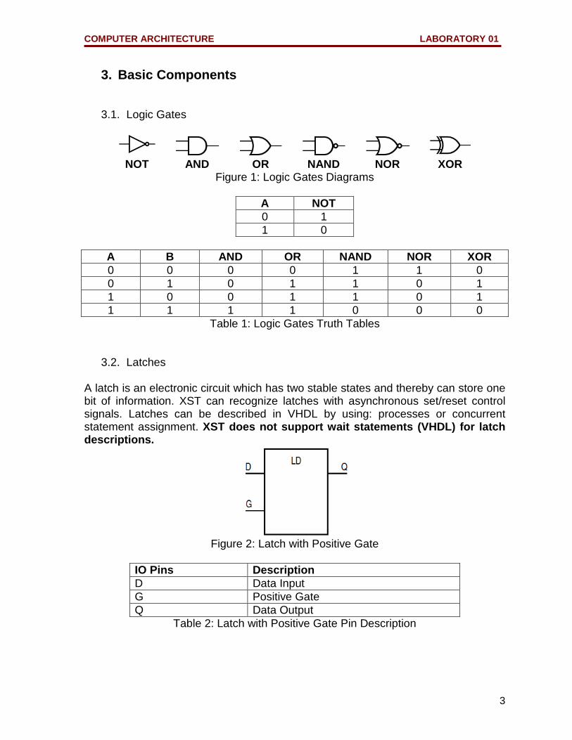
A B AND OR NAND NOR XOR 0 0 0 0 1 1 0 0 1 0 1 1 0 1 1 0 0 1 1 0 1 1 1 1 1 0 0 0
Table 1: Logic Gates Truth Tables
3.2. Latches A latch is an electronic circuit which has two stable states and thereby can store one bit of information. XST can recognize latches with asynchronous set/reset control signals. Latches can be described in VHDL by using: processes or concurrent statement assignment. XST does not support wait statements (VHDL) for latch descriptions.
Figure 2: Latch with Positive Gate
IO Pins Description D Data Input G Positive Gate Q Data Output
Table 2: Latch with Positive Gate Pin Description
3
COMPUTER ARCHITECTURE LABORATORY 01
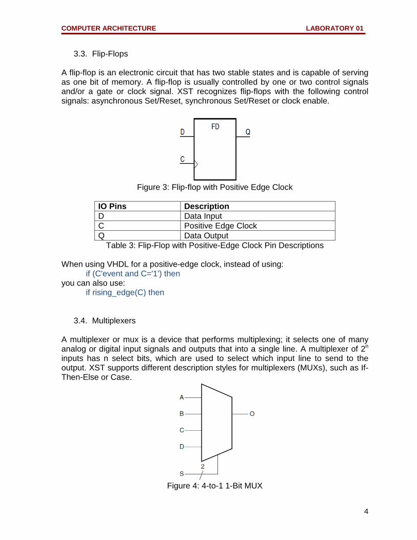
3.3. Flip-Flops A flip-flop is an electronic circuit that has two stable states and is capable of serving as one bit of memory. A flip-flop is usually controlled by one or two control signals and/or a gate or clock signal. XST recognizes flip-flops with the following control signals: asynchronous Set/Reset, synchronous Set/Reset or clock enable.
Figure 3: Flip-flop with Positive Edge Clock
IO Pins Description D Data Input C Positive Edge Clock Q Data Output
Table 3: Flip-Flop with Positive-Edge Clock Pin Descriptions When using VHDL for a positive-edge clock, instead of using: if (C'event and C='1') then you can also use: if rising_edge(C) then
3.4. Multiplexers A multiplexer or mux is a device that performs multiplexing; it selects one of many analog or digital input signals and outputs that into a single line. A multiplexer of 2n inputs has n select bits, which are used to select which input line to send to the output. XST supports different description styles for multiplexers (MUXs), such as If-Then-Else or Case.
Figure 4: 4-to-1 1-Bit MUX
4
COMPUTER ARCHITECTURE LABORATORY 01
IO Pins Description A, B, C, D Data Inputs S Mux Selector O Data Output
Table 4: 4-to-1 1-Bit MUX Pin Descriptions
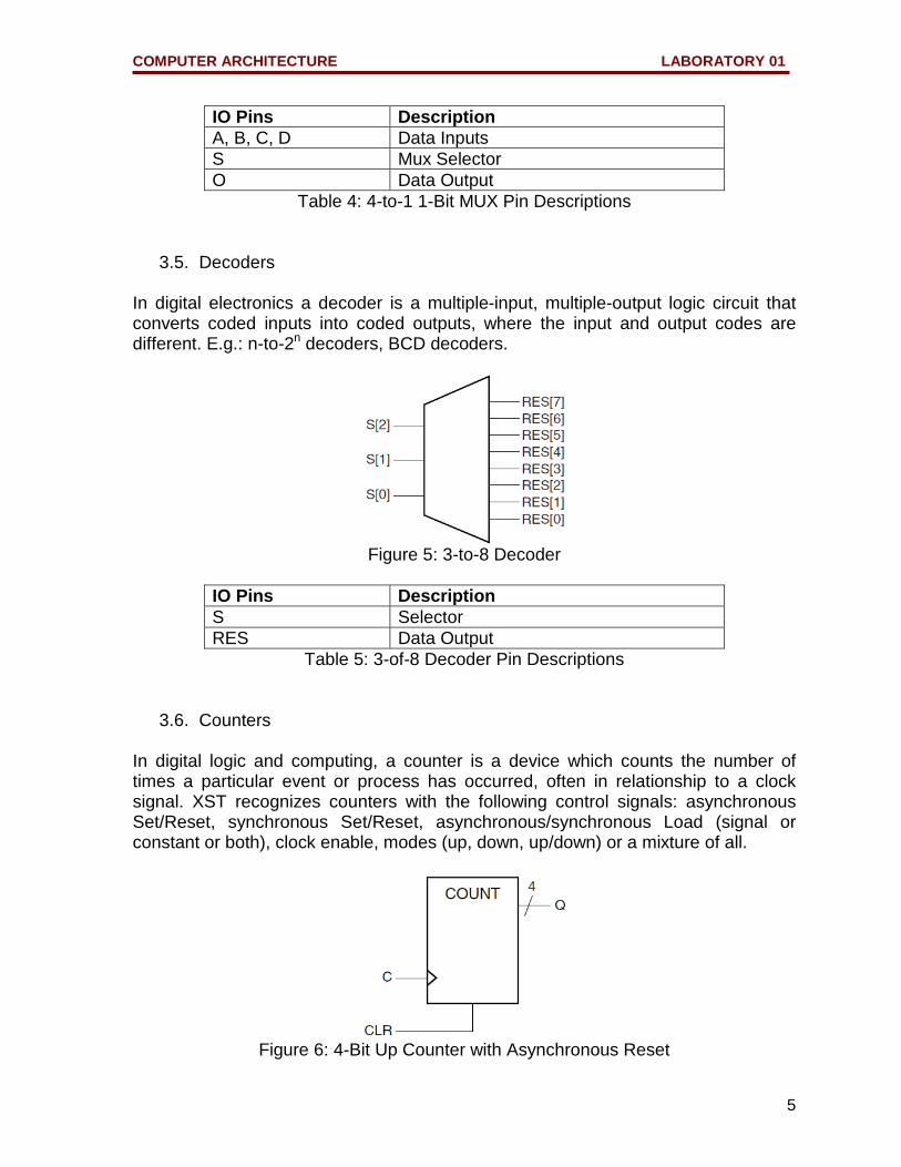
3.5. Decoders In digital electronics a decoder is a multiple-input, multiple-output logic circuit that converts coded inputs into coded outputs, where the input and output codes are different. E.g.: n-to-2n decoders, BCD decoders.
Figure 5: 3-to-8 Decoder
IO Pins Description S Selector RES Data Output
Table 5: 3-of-8 Decoder Pin Descriptions
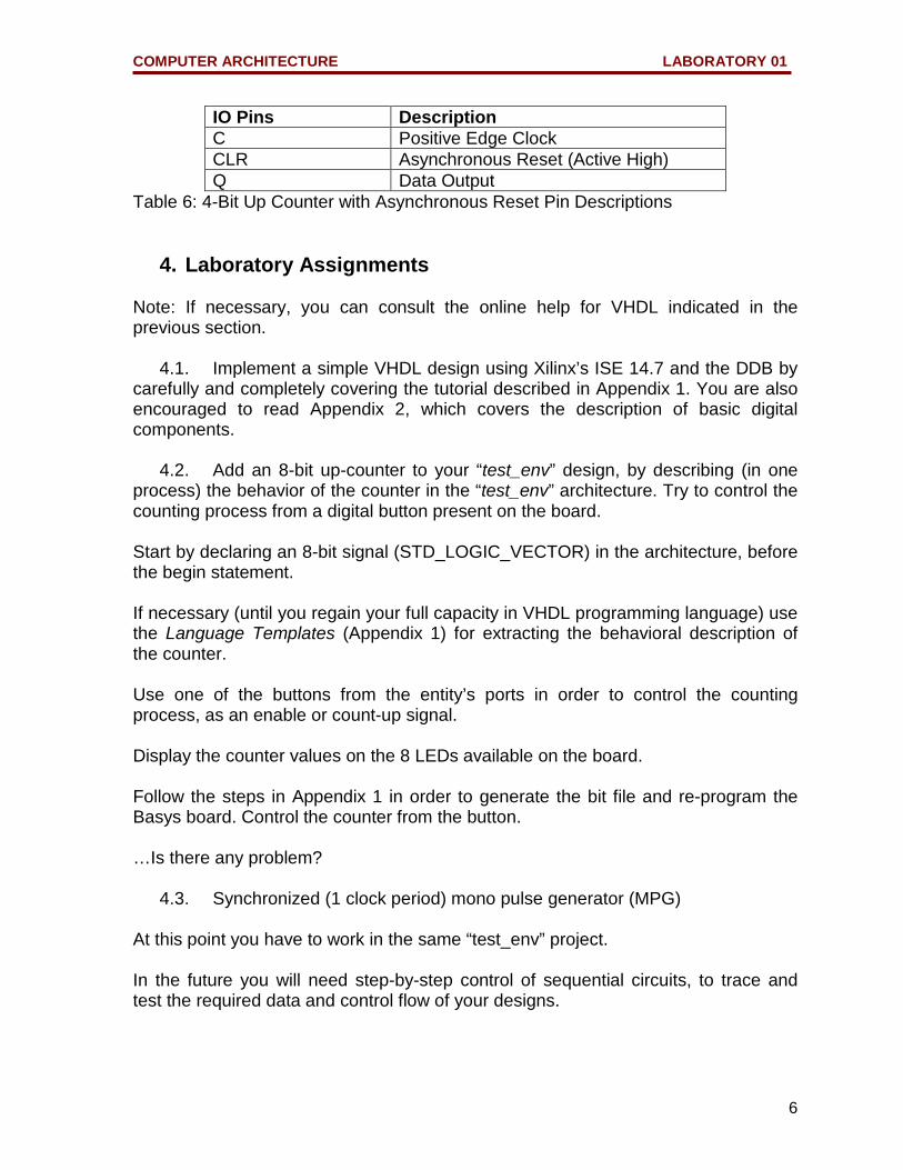
3.6. Counters In digital logic and computing, a counter is a device which counts the number of times a particular event or process has occurred, often in relationship to a clock signal. XST recognizes counters with the following control signals: asynchronous Set/Reset, synchronous Set/Reset, asynchronous/synchronous Load (signal or constant or both), clock enable, modes (up, down, up/down) or a mixture of all.
Figure 6: 4-Bit Up Counter with Asynchronous Reset
5
COMPUTER ARCHITECTURE LABORATORY 01
IO Pins Description C Positive Edge Clock CLR Asynchronous Reset (Active High) Q Data Output
Table 6: 4-Bit Up Counter with Asynchronous Reset Pin Descriptions
4. Laboratory Assignments Note: If necessary, you can consult the online help for VHDL indicated in the previous section.
4.1. Implement a simple VHDL design using Xilinx’s ISE 14.7 and the DDB by carefully and completely covering the tutorial described in Appendix 1. You are also encouraged to read Appendix 2, which covers the description of basic digital components.
4.2. Add an 8-bit up-counter to your “test_env” design, by describing (in one
process) the behavior of the counter in the “test_env” architecture. Try to control the counting process from a digital button present on the board.
Start by declaring an 8-bit signal (STD_LOGIC_VECTOR) in the architecture, before the begin statement. If necessary (until you regain your full capacity in VHDL programming language) use the Language Templates (Appendix 1) for extracting the behavioral description of the counter. Use one of the buttons from the entity’s ports in order to control the counting process, as an enable or count-up signal. Display the counter values on the 8 LEDs available on the board. Follow the steps in Appendix 1 in order to generate the bit file and re-program the Basys board. Control the counter from the button. …Is there any problem?
4.3. Synchronized (1 clock period) mono pulse generator (MPG) At this point you have to work in the same “test_env” project. In the future you will need step-by-step control of sequential circuits, to trace and test the required data and control flow of your designs.
6
COMPUTER ARCHITECTURE LABORATORY 01
The necessary circuit that generates an ENABLE signal once per button push is given in the next figure.
The role of the first register together with the 16-bit counter is to provide a delay necessary to de-bounce the buttons (physically worn out and / or low quality buttons). According to the “degradation” state of the button you may have to increase the size of this 16-bit counter in order to increase the sampling interval for the button signal. The mono pulse generator (MPG) will be implemented in a new entity / new file (menu Project\New Source) and will be used in the “test_env” by declaring as a component in the section for declaring signals and by instantiating this component with port map in the architecture body after begin. The hardware components that implement the MPG (counter, registers, logic gates) will be implemented using the behavioral description: by declaring the necessary signals and by describing the functionality using processes and concurrent assignments in the MPG architecture. Work to do
a. Draw a timing diagram for the above circuit (paper and pencil / blackboard). b. The BTN input is a signal from one of the DDB buttons (BTN0), CLK is the
clock signal of the DDB (50 MHz, you can verify on the board that the jumper is not set for 25 MHz or 100 MHz).
c. Write and check the VHDL code for this circuit. d. Include the MPG component in the test_env. e. Use the ENABLE signal as count up for the previously implemented 8-bit
counter, from section 3.2. You need to add the condition that ENABLE equals ‘1’ where you test the count up condition for the 8-bit counter.
Synthesize your design and do not forget about View RTL Schematic… Load your new design on the Basys board.
7
COMPUTER ARCHITECTURE LABORATORY 01
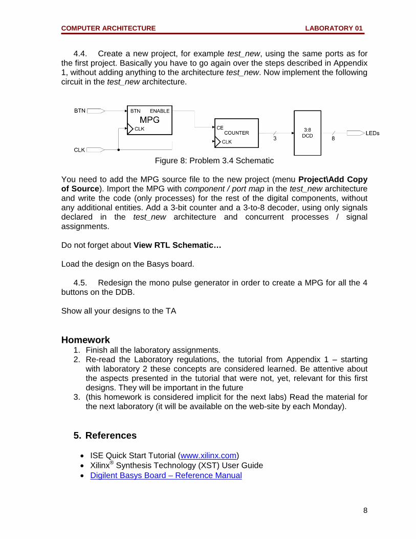
4.4. Create a new project, for example test_new, using the same ports as for the first project. Basically you have to go again over the steps described in Appendix 1, without adding anything to the architecture test_new. Now implement the following circuit in the test_new architecture.
Figure 8: Problem 3.4 Schematic
You need to add the MPG source file to the new project (menu Project\Add Copy of Source). Import the MPG with component / port map in the test_new architecture and write the code (only processes) for the rest of the digital components, without any additional entities. Add a 3-bit counter and a 3-to-8 decoder, using only signals declared in the test_new architecture and concurrent processes / signal assignments. Do not forget about View RTL Schematic… Load the design on the Basys board.
4.5. Redesign the mono pulse generator in order to create a MPG for all the 4 buttons on the DDB. Show all your designs to the TA Homework
1. Finish all the laboratory assignments. 2. Re-read the Laboratory regulations, the tutorial from Appendix 1 – starting
with laboratory 2 these concepts are considered learned. Be attentive about the aspects presented in the tutorial that were not, yet, relevant for this first designs. They will be important in the future
3. (this homework is considered implicit for the next labs) Read the material for the next laboratory (it will be available on the web-site by each Monday).
5. References
• ISE Quick Start Tutorial (www.xilinx.com) • Xilinx® Synthesis Technology (XST) User Guide • Digilent Basys Board – Reference Manual
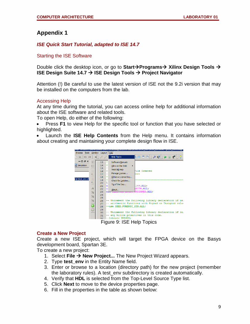
Appendix 1 ISE Quick Start Tutorial, adapted to ISE 14.7 Starting the ISE Software Double click the desktop icon, or go to StartPrograms Xilinx Design Tools ISE Design Suite 14.7 ISE Design Tools Project Navigator Attention (!) Be careful to use the latest version of ISE not the 9.2i version that may be installed on the computers from the lab. Accessing Help At any time during the tutorial, you can access online help for additional information about the ISE software and related tools. To open Help, do either of the following: • Press F1 to view Help for the specific tool or function that you have selected or highlighted. • Launch the ISE Help Contents from the Help menu. It contains information about creating and maintaining your complete design flow in ISE.
Figure 9: ISE Help Topics
Create a New Project Create a new ISE project, which will target the FPGA device on the Basys development board, Spartan 3E. To create a new project:
1. Select File New Project... The New Project Wizard appears. 2. Type test_env in the Entity Name field. 3. Enter or browse to a location (directory path) for the new project (remember
the laboratory rules). A test_env subdirectory is created automatically. 4. Verify that HDL is selected from the Top-Level Source Type list. 5. Click Next to move to the device properties page. 6. Fill in the properties in the table as shown below:
9
COMPUTER ARCHITECTURE LABORATORY 01
Product Category: All Family: Spartan 3E Device: XC3S100E Package: TQ144 Speed Grade: -4 Top-Level Module Type: HDL Synthesis Tool: XST (VHDL/Verilog) Simulator: ISim (VHDL/Verilog) Preferred language: VHDL Leave the default values in the remaining fields.
Creating a VHDL Source Create a VHDL source file for the project as follows:
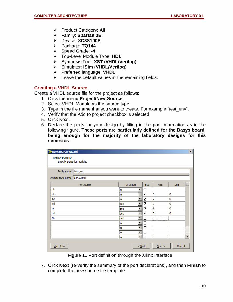
1. Click the menu Project/New Source. 2. Select VHDL Module as the source type. 3. Type in the file name that you want to create. For example “test_env”. 4. Verify that the Add to project checkbox is selected. 5. Click Next. 6. Declare the ports for your design by filling in the port information as in the
following figure. These ports are particularly defined for the Basys board, being enough for the majority of the laboratory designs for this semester.
Figure 10 Port definition through the Xilinx Interface
7. Click Next (re-verify the summary of the port declarations), and then Finish to
complete the new source file template.
10
COMPUTER ARCHITECTURE LABORATORY 01
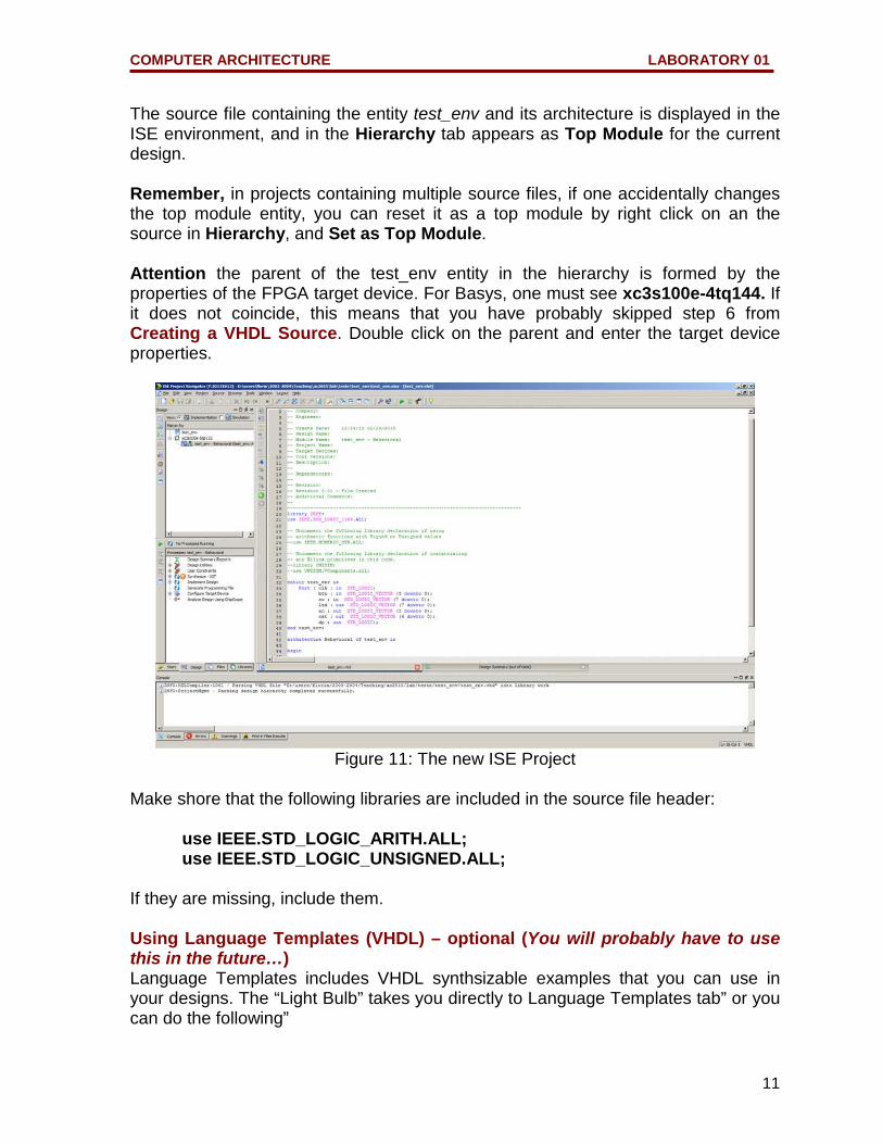
The source file containing the entity test_env and its architecture is displayed in the ISE environment, and in the Hierarchy tab appears as Top Module for the current design. Remember, in projects containing multiple source files, if one accidentally changes the top module entity, you can reset it as a top module by right click on an the source in Hierarchy, and Set as Top Module. Attention the parent of the test_env entity in the hierarchy is formed by the properties of the FPGA target device. For Basys, one must see xc3s100e-4tq144. If it does not coincide, this means that you have probably skipped step 6 from Creating a VHDL Source. Double click on the parent and enter the target device properties.
Figure 11: The new ISE Project
Make shore that the following libraries are included in the source file header:
use IEEE.STD_LOGIC_ARITH.ALL; use IEEE.STD_LOGIC_UNSIGNED.ALL;
If they are missing, include them. Using Language Templates (VHDL) – optional (You will probably have to use this in the future…) Language Templates includes VHDL synthsizable examples that you can use in your designs. The “Light Bulb” takes you directly to Language Templates tab” or you can do the following”
11
COMPUTER ARCHITECTURE LABORATORY 01
1. Place the cursor under the begin statement of your architecture. 2. Open Language Templates by selecting the menu Edit Language
Templates… 3. Navigate in the hierarchy “+”, to the coding examples:
VHDL Synthesis Constructs Coding Examples … 4. Select the desired component in the hierarchy, then right click Use in File.
This step will copy the model code to your source file at the place of your cursor.
5. Close the Language Templates. 6. Change the signal names so that they will match the signals in your entity.
Editing the VHDL Source Code
1. Add component and/or signal declarations between the architecture and the begin statements.
2. Add the rest of the code (component instantiation, behavioral description, etc.) after the begin statement and before the end statement.
3. For the first example add the following statements after begin. led <= sw; an <= btn; cat <= (others=>'0'); dp <= '0';
4. Save the file by selecting File Save or Ctrl + S. 5. Select the top level entity in the Hierarchy tab: test_env. 6. Verify that your VHDL syntax is correct: in the Processes zone: Synthesize
– XST Check Syntax Run 7. Correct the errors if they appear in the bottom part of the ISE environment.
Start from the top with the first error. 8. Synthesize your design: double click Synthesize – XST 9. View the resulting circuit: double click Synthesize – XST View RTL
Schematic. In the next dialog be sure to select the second variant (Start with a schematic of the top level block), press OK. The top level entity will appear. Double click to view its internal organization. You should recognize at least a part of the declared entity. This is a first method to verify that your code is correct and implements the desired circuits.
You have now created the VHDL source for the “test_env” project with no errors. Note: You can also create a UCF file for your project by selecting Project Create New Source. Assigning Pin Location Constraints Specify the pin locations for the ports of the design so that they are connected correctly on the DDB. You can Edit the User Constraints File (*.ucf) manually (Users Constraints Edit Constraints (Text)). You can find the user constraints file here.
Download the file and add it to your design. Open the constraints file and see the syntax for every port (net). For the future, you can add new ports to the constraints file. Implement Design and Verify Constraints Implement the design and verify that it meets all constraints.
1. Double-click the Implement Design process in the Processes tab. 2. Notice that after Implementation is complete, the Implementation processes
have a green check mark next to them indicating that they completed successfully without Errors or Warnings. If there are errors or warnings you can correct them.
3. Open Design Summary/Reports. Analyze the reports of your design (Summary, Timing Constraints, etc.). In the next designs these reports will be relevant.
Generate Programming File
1. Before generating the programming file you must set the start-up clock option to JTAG clock: Generate Programming File Properties Startup Options FPGA Start-Up Clock JTAG Clock.
2. Generate the programming file: double click Generate Programming File. The bit file for the DDB configuration is created.
If you notice that one or more processes have an orange question mark next to them, it indicates that they are out-of-date with one or more of the design files. You will have to re-run these processes. If there are no errors at this time the file “test_env.bit” should be in the project folder.
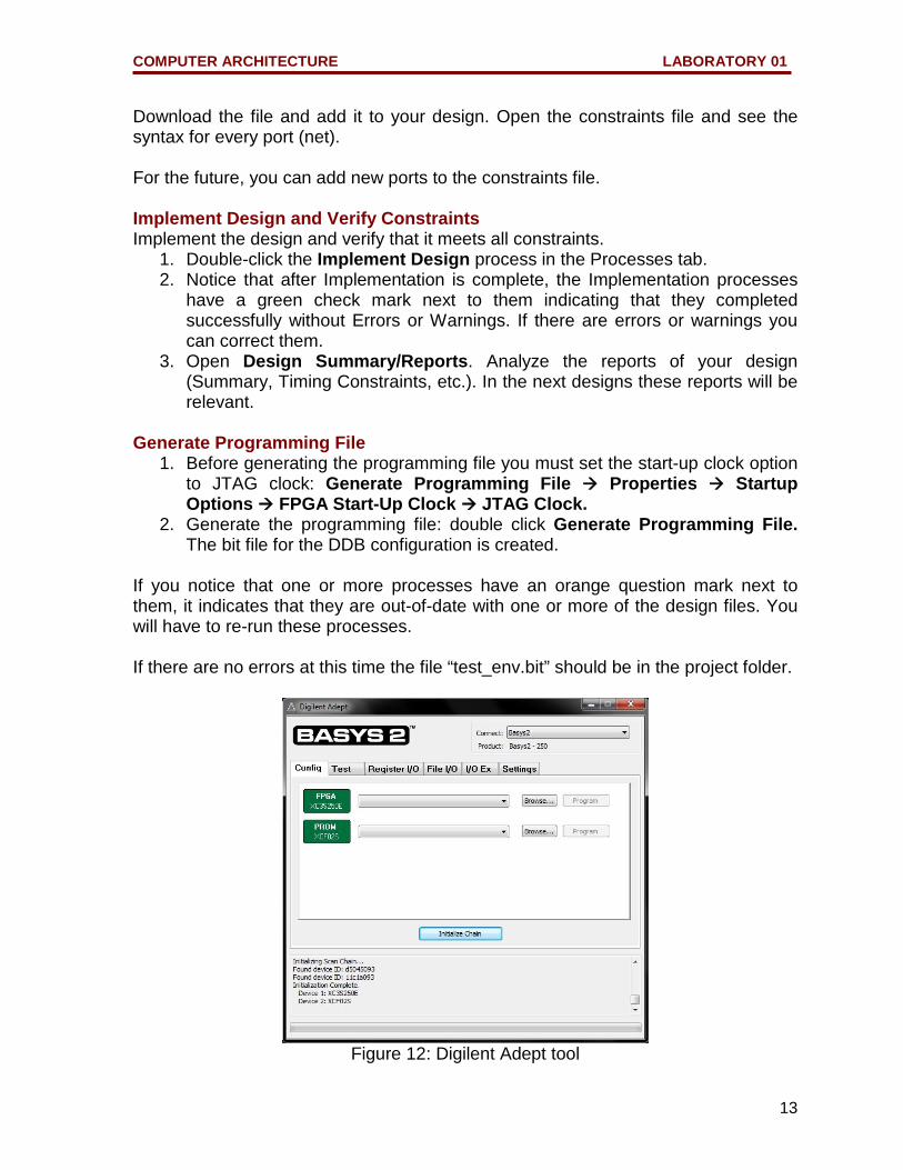
Figure 12: Digilent Adept tool
13
COMPUTER ARCHITECTURE LABORATORY 01
Download Design to the Spartan™-3E Demo Board Basys If you encounter problems during the programming of the board please go to the end of this tutorial (after the following figure).
1. Connect the Basys board to the USB port. 2. Start the Adept Tool from Adept programming software: Start Programs
Digilent Adept (Figure 6). 3. Press the Initialize Chain button 4. Browse for the project’s bit file. 5. Program the FPGA device.
Possible problems when connecting the board and solutions: Problem: The Basys board is not recognized. Solutions (Start in order and restart Adept after every fail, ask the TA to assist you):
a) Try a different USB port (front or rear of the computer). If a driver install process initiates call your TA. You will need administrative privileges.
b) Verify that the board does not require external power.
• If it does not require external power (no “E” sign – see the figure below
position 1), make shore that the switch (Position 3 in the image) is in the VUSB position
• If it requires external power, do the following
Use a 3.3 V power supply in the external power socket (position 2 in the image)
Move the switch (position 3 in the image) to the VEXT position c) Try a new programming cable d) Try a new board (report this to your TA) e) Change the workstation