ELSEVIER Journal of Electrostatics 42 (1998) 333-350
Journal of
ELECTROSTATICS
CMOS-on-SOI ESD protection networks 1
S. V o l dma n a'*, R. Schulz b, J. H o w a r d a, V. Gross ~, S. W u c, A. Yapsiff, D. Sadana ~, H. HoveF, J. Walke r b, F. Assaderaghi ¢, B. Chen b, J.Y-C Sun ~,
G. Shahidi c
a IBM Microelectronics Division, Dept. M65, Bldg. 972-1 Col. B6, Essex Junction, VT 05452, USA b IBM Hopewell Junction, NY, USA
¢ IBM Watson Research, Yorktown Heights, N. Y., USA
Received 13 November 1996; received in revised form 20 April 1997; accepted 20 May 1997
MOSFET scaling on bulk silicon has been the primary focus of the semiconductor and microelectronics industry for achieving CMOS chip performance and density objectives. The shrinking of MOSFET dimensions for high density, low power and enhanced performance requires reduced power-supply voltages [1, 2]. Because power consumption, P, is a function of capacitance, C, power supply voltage, V, and transition frequency, f, where P = C V 2, the focus has been on reducing both C and V as the transition frequency increases. The components of the MOSFET capacitance (C) consist of diffusion and gate capacitances. As a result, dielectric thickness and channel length are scaled with power-supply voltage. Power-supply reduction con- tinues to be the trend for future low-voltage CMOS. However, with power-supply reduction, transistor performance is severely impacted by both junction capacitance
334 S. Voldman et al./Journal of Electrostatics 42 (1998) 333-350
and the MOSFET body effect at lower voltages [3]. As technologies scale below 0.25-~tm channel lengths, to 0.15 and 0.1 ktm, short-channel effects (SCE) control, gate resistance, channel profiling and other barriers become an issue for advanced CMOS technologies. While significant success has been achieved with successive scaling of bulk CMOS technology, the manufacturing control issues and power consumption will become more difficult to deal with.
Using silicon-on-insulator (SO1) substrates, many of the concerns and obstacles of bulk-silicon CMOS can be eliminated at low power-supply voltages. CMOS-on-SOI has significant advantages over bulk CMOS technology, and will achieve the scaling objectives of low power and high performance for future technologies [3]. CMOS- on-SO1 provides low power consumption, low leakage current, low capacitance diode structures, good sub-threshold I - V characteristics (better than 60 mV/decade), a low soft error rate from both alpha particles and cosmic rays, good SRAM access times, and other technology benefits [4]. SOI has not become a mainstream CMOS technology because of the rapid improvement in bulk CMOS technology perfor- mance, however, it is a future contender for mainstream CMOS applications. One of the barriers to implementing SO1 is the "floating body" issue [5]. Another barrier is electrostatic discharge protection (ESD). ESD protection of SO1 structures has been of interest for silicon-on-sapphire (SOS) and SO1 applications for quite some time [6]. In early SOS/SO1 literature, SOS and SO1 were regarded as costly, having low volume, and capable of exotic applications where ESD robustness was more of a curiosity than a manufacturing necessity or supplier objective. Recently, ESD analysis has increased as SO1 becomes a mainstream direction for advanced CMOS development [7-10].
Presently, there are multiple strategies for ESD protection of SO1 structures. One of these is to use bulk ESD protection circuits on an SO1 wafer. From a semiconductor process proposed by Kawai [11], bulk transistors are in the substrate and SO1 transistors on the insulating film. If this is possible, bulk ESD devices can be designed without any new SOl-specific ESD issues. This proposal has significant topography, which would make it unacceptable for high density and planarity integration issues. In addition, it forces special semiconductor processing for the sole purpose of providing ESD protection. Sun proposed a mixed thin film where ESD devices are constructed in the bulk and where the oxygen implant is masked and SO1 devices are built over the insulating layer [12]. This concept eliminates planarity concerns but leads to silicon dislocation, which is unacceptable from a manufacturing perspective. A disadvantage of these bulk strategies is that charged-device model (CDM) failures can occur more frequently because ESD networks now are in bulk, whereas in an SO1 technology, bulk substrate charging from CDM mechanisms is less of a concern. With SOI, significant freedom exists to develop bipolar technology side-by-side with CMOS technology. A significant cost results in each of these implementations, which is neither acceptable nor practical to address.
The extension of known circuits into SO1 ESD protection networks has been proposed for these networks. SO1 ESD schemes have included gated double-diode networks, floating body/grounded gate MOSFET networks, grounded body/grounded gate MOSFET networks and lateral bipolar elements [13-17]. Gated-diode structures,
S. Voldman et al./Journal of Electrostatics 42 (1998) 333-350 335
formed from transistor elements, can also be used for ESD designs. Lu states that floating-body SO1 transistors are superior to gated-diode SO1 networks because of lower initial breakdown voltage. Although ESD networks were discussed, ESD robustness levels for todays mainstream CMOS technology were not shown.
This paper shows that ESD robustness in simple CMOS-on-SOI ESD protection circuits can be achieved which are acceptable for semiconductor chip manufacturing. ESD results will demonstrate ESD robustness in a mainstream scaled 0.254).15 ~tm channel length shallow-trench isolated (STI) CMOS-on-SOI technology. Advantages and disadvantages of ESD protection in SO1 are discussed from an ESD design perspective. Our first objective was to show whether ESD robustness can be achieved using standard ESD networks in the CMOS-on-SOI technology for both positive- and negative-mode ESD protection. A second objective was to determine what types of ESD structures are successful in CMOS-on-SOI. The third was to understand how ESD robustness scales with design parameters such as channel length, channel width, gate polarity, and body contact resistance. Additionally, ESD robustness versus channel length and width of CMOS-on-SOI n-channel and p-channel transistors were studied. First, however, we discuss the CMOS-on-SOI technology, where MOSFET ESD robustness is shown as a function of design parameters. ESD protection circuits, design layout and ESD robustness results are also provided for the specific implementations.
2. CMOS-on-SOI versus bulk ESD design practices
There are both advantages and disadvantages to designing ESD protection devices in CMOS-on-SOI compared to bulk silicon in the areas of design flexibility, semicon- ductor process scaling, semiconductor device reliability, chip functionality, ESD networks, etc.
One of the many advantages of designing ESD networks in SOl is that full dielectric isolation allows electrically isolated circuits to handle high voltages and low-voltage CMOS circuits on the same chip. CMOS-on-SOI ESD protection circuits eliminate salicide-metallurgical junction penetration concerns from ESD testing. Titanium salicide penetrates metallurgical junctions at isolation edges and at the bottom of source/drain junctions in highly-scaled advanced CMOS technologies. Another ad- vantage of SO1 ESD networks is that they lack any of the concerns pertaining to bulk CMOS latchup. Many bulk CMOS ESD strategies use parasitic pnpn structures which provide both ESD protection and latchup (under the right conditions). Guard rings are also not required in CMOS-on-SOI ESD networks. These prevent leakage- induced threshold shifts, latchup, and overshoot-undershoot injection in both I/O and ESD networks in bulk CMOS whereas in CMOS-on-SOI this is not a concern. Another SO1 advantage is the flexibility gained by using n-channel or p-channel source/drain implants for diode structures in the ESD networks. Because there is no advantage to large area diodes, SO1 ESD structures can be scaled to minimum-design rule perimeter-dominant designs that achieve low capacitance.
While designing ESD networks in SO1 has advantages, there are some func- tional tradeoffs. The advantage of SO1 ESD design is low source/drain and diode
336 S. Voldman et al./Journal of Electrostatics 42 (1998) 333-350
capacitance; the disadvantage is the increase in gate perimeter capacitance. Although thermal dissipation for both off-chip drivers and ESD protection networks is a disad- vantage of SO1 technology, limitations on lateral thermal transport in bulk shallow- trench isolation (STI) CMOS technology already exists with ESD results well over 8 kV demonstrated. The problem of thermal dissipation can be solved by using wide perimeter designs styles as well as metallurgy and contacts to remove the self-heating in the ESD structure. In addition, as SOl technology scales, the thermal resistance of the silicon dioxide film decreases with thinner SiO2 films, thereby allowing for better thermal dissipation to the bulk substrate; a fact already noted by the power elec- tronics-on-SO1 industry. In SOl technology, achieving negative pulse ESD robustness is as difficult as achieving positive pulse ESD robustness. In bulk silicon, using comparatively smaller structures, ESD protection for negative mode pulses is easily achieved because of current dissipation to the bulk substrate; in SOI this does not occur. This forces designers to allocate as much area for negative mode as the positive mode protection schemes. Fortunately, when scaling designs from the 5.0 V tolerant/ 3.3 V to a 2.5 V tolerant/1.8 V mixed-voltage interface environment, fewer diodes are needed between mixed power supplies. Substrate charging, which initiates the charged-device model (CDM) concern, will be less of a concern to small internal circuits in CMOS-on-SOI constructed on thick silicon dioxide films. Although ESD robustness is believed to significantly decrease from bulk CMOS to CMOS-on-SO1, there are technology scaling advantages of SO1 networks that can be utilized.
3. CMOS-on-SOI technology
CMOS-on-SOI technology allows for the mapping of standard advanced technolo- gies into an SO1 technology without significant modifications. SOI process techniques include epitaxial lateral overgrowth (ELO), lateral solid-phase epitaxy (LSPE) and full isolation by porous oxidized silicon (FIPOS). In our experimentation, ESD networks were constructed using the semiconductor process of separation by implanted oxygen (SIMOX) and wafer-bonding and etch-back (SIBOND) because they achieve low defect density, thin film control, long minority carrier lifetimes and good channel mobility characteristics [5].
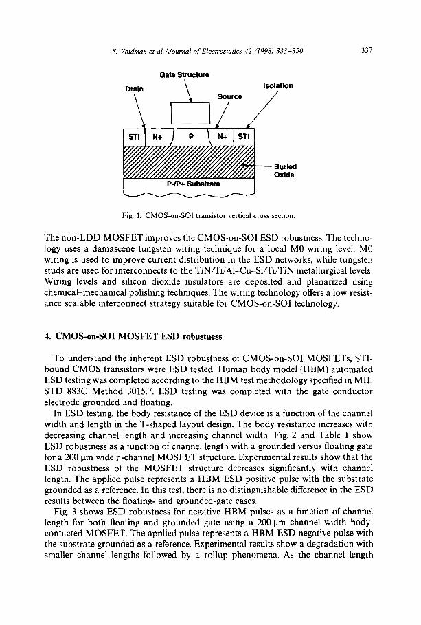
In this paper, the first experimental CMOS-on-SOI technology is a 2.5 V logic technology [18]. Fig. 1 shows the vertical cross section ofa CMOS-on-SOI transistor. The MOSFET transistor has a 0.25-/am effective channel length. Structural features are defined by shallow-trench isolation (STI) which abutts the silicon dioxide film in the vertical profile, fully isolating the transistor structures. Shallow-trench isolation eliminates planarity concerns and multidimensional oxidation effects, such as LOCOS bird's beak, thereby allowing technology migration and scaling to sub-0.25- lam technologies. Device-channel lengths are obtained using a 0.5 numerical aperture (NA) 245 nm step-and-scan tool and negative tone resist system. Dual workfunctions silicided polysilicon gate electrodes are used for the gate conductor. P-channel transistors use boron junctions. N-channel transistors have non-LDD abrupt arsenic junctions. Non-LDD transistors are possible as a result of the power supply scaling.
S. Voldman et al./Journal of Electrostatics 42 (1998) 333-350 337
The non-LDD MOSFET improves the CMOS-on-SOI ESD robustness. The techno- logy uses a damascene tungsten wiring technique for a local M0 wiring level. M0 wiring is used to improve current distribution in the ESD networks, while tungsten studs are used for interconnects to the TiN/Ti/A1-Cu-Si/Ti/TiN metallurgical levels. Wiring levels and silicon dioxide insulators are deposited and planarized using chemical-mechanical polishing techniques. The wiring technology offers a low resist- ance scalable interconnect strategy suitable for CMOS-on-SOI technology.
4. CMOS-on-SOI MOSFET ESD robustness
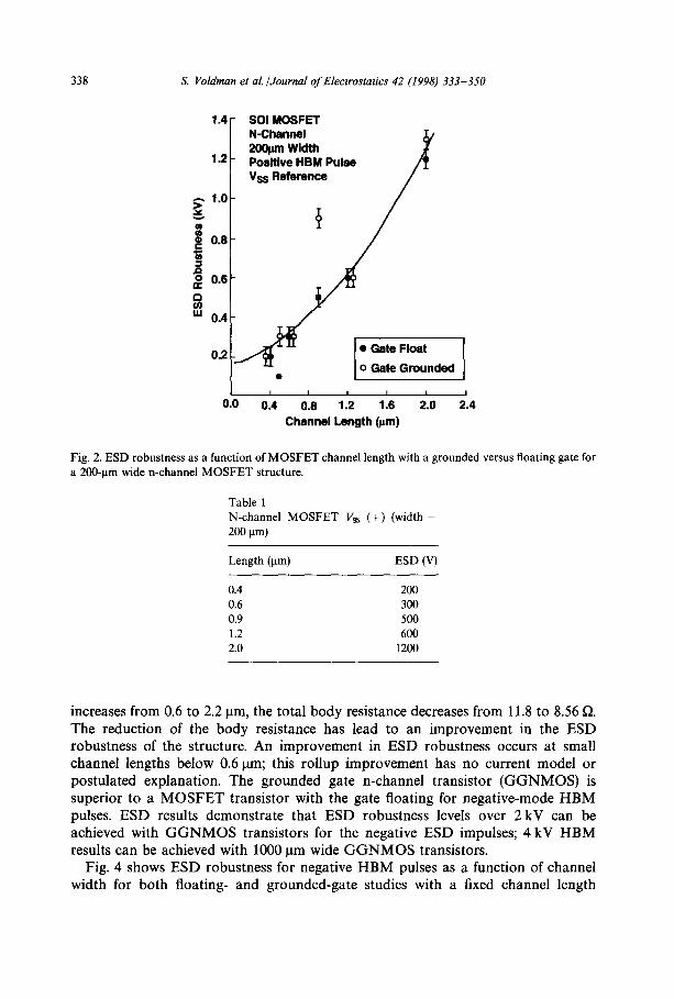
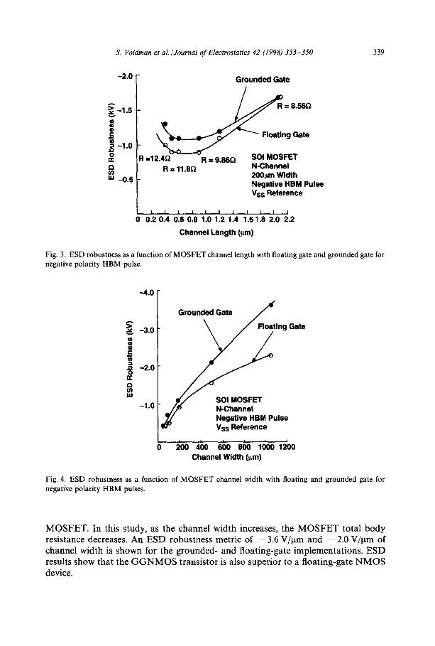
To understand the inherent ESD robustness of CMOS-on-SOI MOSFETs, STI- bound CMOS transistors were ESD tested. Human body model (HBM) automated ESD testing was completed according to the HBM test methodology specified in MIL STD 883C Method 3015.7. ESD testing was completed with the gate conductor electrode grounded and floating.
In ESD testing, the body resistance of the ESD device is a function of the channel width and length in the T-shaped layout design. The body resistance increases with decreasing channel length and increasing channel width. Fig. 2 and Table 1 show ESD robustness as a function of channel length with a grounded versus floating gate for a 200 pm wide n-channel MOSFET structure. Experimental results show that the, ESD robustness of the MOSFET structure decreases significantly with channel length. The applied pulse represents a HBM ESD positive pulse with the substrate grounded as a reference. In this test, there is no distinguishable difference in the ESD results between the floating- and grounded-gate cases.
Fig. 3 shows ESD robustness for negative HBM pulses as a function of channel length for both floating and grounded gate using a 200 pm channel width body- contacted MOSFET. The applied pulse represents a HBM ESD negative pulse with the substrate grounded as a reference. Experimental results show a degradation with smaller channel lengths followed by a rollup phenomena. As the channel length
338 S. Voldman et al. /Journal of Electrostatics 42 (1998) 333-350
1.4
1.2
1.0 v
~ 0.8
~ 0.6
w 0.4
0.2
0.0 014
SOl MOSFET N-Channel ~/ 2001un Width ) ~ Positive HBM Pulse / ~ V
"~ o Gate Grounded
I
0.8 1~2 116 2L.0 Channel Length (~m)
Fig. 2. ESD robustness as a function of M O S F E T channel length with a grounded versus floating gate for a 200-1am wide n-channel M O S F E T structure.
Table 1 N-channel M O S F E T Vss (+ ) (width = 200 lam)
Length (~tm) ESD (V)
0.4 200 0.6 300 0.9 500 1.2 600 2.0 1200
increases from 0.6 to 2.2 tam, the total body resistance decreases from 11.8 to 8.56 f~. The reduction of the body resistance has lead to an improvement in the ESD robustness of the structure. An improvement in ESD robustness occurs at small channel lengths below 0.6 ~tm; this rollup improvement has no current model or postulated explanation. The grounded gate n-channel transistor (GGNMOS) is superior to a MOSFET transistor with the gate floating for negative-mode HBM pulses. ESD results demonstrate that ESD robustness levels over 2 kV can be achieved with GGNMOS transistors for the negative ESD impulses; 4 kV HBM results can be achieved with 1000 lam wide GGNMOS transistors.
Fig. 4 shows ESD robustness for negative HBM pulses as a function of channel width for both floating- and grounded-gate studies with a fixed channel length
S. Voldman et al./Journal of Electrostatics 42 (1998) 333-350 339
-2 .0
A
>~ -1 .5
@
: -1 .0 .Q o rr a GO "' -0.5
Grounded Gate
~ = 8.56Q
~ Floating Gate
! =12.4Q R = 9 ,862 SOl MOSFET R = 11.8~ N-Channel
Fig. 4. ESD robustness as a function of MOSFET channel width with floating and grounded gate for negative polarity HBM pulses.
M O S F E T . In this s tudy, as the channel width increases, the M O S F E T to ta l b o d y resis tance decreases. An E S D robus tness metr ic of - 3 . 6 V/~tm and - 2 . 0 V/~tm of channel width is shown for the g rounded- and f loa t ing-gate implementa t ions . E S D results show tha t the G G N M O S t rans i s to r is also super ior to a f loa t ing-gate N M O S device.
340 S. Voldman et aL /Journal of Electrostatics 42 (1998) 333-350
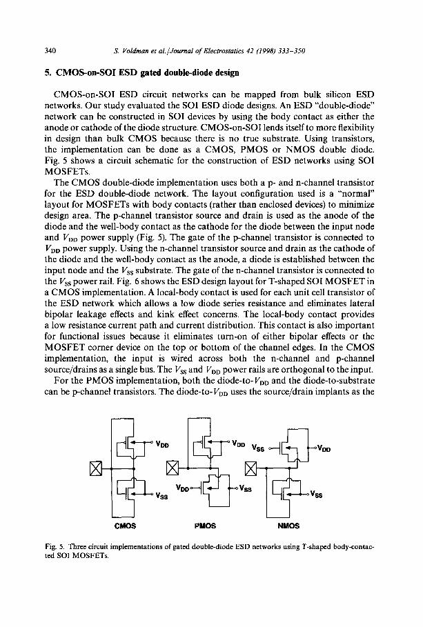
5. CMOS-on-SOI ESD gated double-diode design
CMOS-on-SOI ESD circuit networks can be mapped from bulk silicon ESD networks. Our study evaluated the SO1 ESD diode designs. An ESD "double-diode" network can be constructed in SO1 devices by using the body contact as either the anode or cathode of the diode structure. CMOS-on-SOI lends itself to more flexibility in design than bulk CMOS because there is no true substrate. Using transistors, the implementation can be done as a CMOS, PMOS or NMOS double diode. Fig. 5 shows a circuit schematic for the construction of ESD networks using SOl MOSFETs.
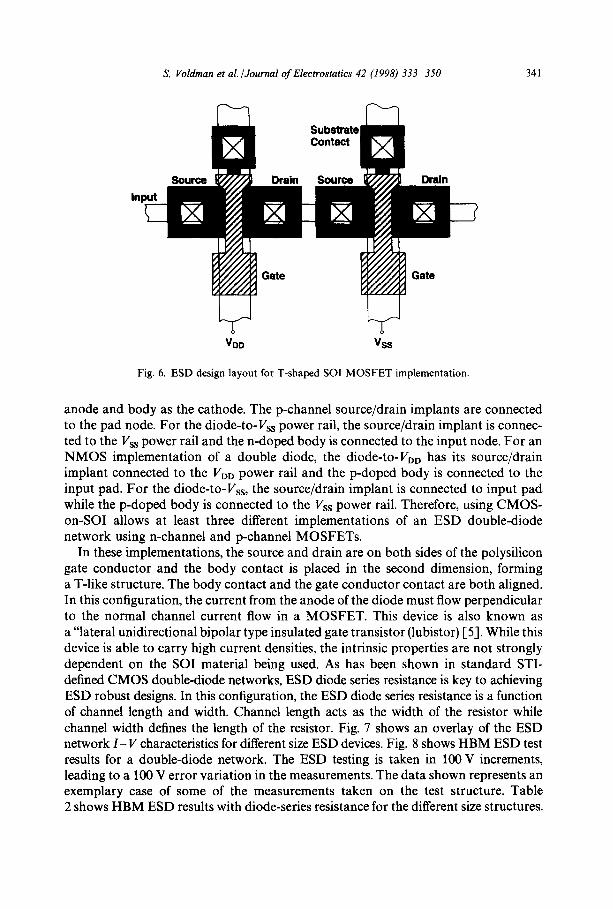
The CMOS double-diode implementation uses both a p- and n-channel transistor for the ESD double-diode network. The layout configuration used is a "normal" layout for MOSFETs with body contacts (rather than enclosed devices) to minimize design area. The p-channel transistor source and drain is used as the anode of the diode and the well-body contact as the cathode for the diode between the input node and VDO power supply (Fig. 5). The gate of the p-channel transistor is connected to VDD power supply. Using the n-channel transistor source and drain as the cathode of the diode and the well-body contact as the anode, a diode is established between the input node and the Vss substrate. The gate of the n-channel transistor is connected to the Vss power rail. Fig. 6 shows the ESD design layout for T-shaped SO1 MOSFET in a CMOS implementation. A local-body contact is used for each unit cell transistor of the ESD network which allows a low diode series resistance and eliminates lateral bipolar leakage effects and kink effect concerns. The local-body contact provides a low resistance current path and current distribution. This contact is also important for functional issues because it eliminates turn-on of either bipolar effects or the MOSFET corner device on the top or bottom of the channel edges. In the CMOS implementation, the input is wired across both the n-channel and p-channel source/drains as a single bus. The Vss and VDD power rails are orthogonal to the input.
For the PMOS implementation, both the diode-to-VDD and the diode-to-substrate can be p-channel transistors. The diode-to-VoD uses the source/drain implants as the
CMOS
Voo -J ov. PMOS NMOS
Fig. 5. Three circuit implementations of gated double-diode ESD networks using T-shaped body-contac- ted SO1 MOSFETs.
S. Voldman et aL /Journal of Electrostatics 42 (1998) 333-350 341
Inl
VDD Vss
Fig. 6. ESD design layout for T-shaped SOI MOSFET implementation.
anode and body as the cathode. The p-channel source/drain implants are connected to the pad node. For the diode-to-Vss power rail, the source/drain implant is connec- ted to the Vss power rail and the n-doped body is connected to the input node. For an NMOS implementation of a double diode, the diode-to-VDD has its source/drain implant connected to the VDD power rail and the p-doped body is connected to the input pad. For the diode-to-Vss, the source/drain implant is connected to input pad while the p-doped body is connected to the Vss power rail. Therefore, using CMOS- on-SO1 allows at least three different implementations of an ESD double-diode network using n-channel and p-channel MOSFETs.
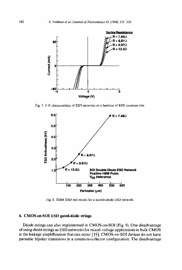
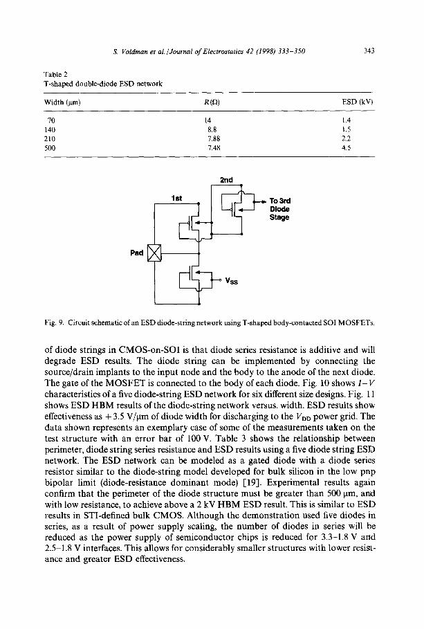
In these implementations, the source and drain are on both sides of the polysilicon gate conductor and the body contact is placed in the second dimension, forming a T-like structure. The body contact and the gate conductor contact are both aligned. In this configuration, the current from the anode of the diode must flow perpendicular to the normal channel current flow in a MOSFET. This device is also known as a "lateral unidirectional bipolar type insulated gate transistor (lubistor) [5]. While this device is able to carry high current densities, the intrinsic properties are not strongly dependent on the SOI material being used. As has been shown in standard STI- defined CMOS double-diode networks, ESD diode series resistance is key to achieving ESD robust designs. In this configuration, the ESD diode series resistance is a function of channel length and width. Channel length acts as the width of the resistor while channel width defines the length of the resistor. Fig. 7 shows an overlay of the ESD network I - V characteristics for different size ESD devices. Fig. 8 shows HBM ESD test results for a double-diode network. The ESD testing is taken in 100 V increments, leading to a 100 V error variation in the measurements. The data shown represents an exemplary case of some of the measurements taken on the test structure. Table 2 shows HBM ESD results with diode-series resistance for the different size structures.
342 S. Voldman et al. /Journal o f Electrostatics 42 (1998) 333-350
80
< E v
= --80
(.1
I
-5
,f, o
Voltage (V)
I I I I
5
Series Resistance
~ R = 7.48Q ' R = 8.87Q
R = 8.97f~ / / R = 13.3~
Fig. 7. I - V characteristics of ESD networks as a function of ESD structure size.
6.0
5.0 A > J g "- ' 4.0 W W @ ( =
3.0
O Ilc
O 2.0 ¢,n I l l
1.0
R = 7.48f~
. ~ ~ . R = 8.97~
R = 13.3Q SOl Double-Diode ESD Network Positive HBM Pulse VDD Reference
I I I I I I
1 O0 200 300 400 500 600
Perimeter (pm)
Fig. 8. H B M ESD test results for a double-diode ESD network.
6. CMOS-on-SOI ESD gated-diode strings
Diode strings can also implemented in CMOS-on-SOI (Fig. 9). One disadvantage of using diode strings as ESD networks for mixed-voltage applications in bulk CMOS is the leakage amplifiication that can occur [19J. CMOS-on-SOI devices do not have parasitic bipolar transistors in a common-collector configuration. The disadvantage
S. Voldman et al./Journal of Electrostatics 42 (1998) 333-350
Table 2 T-shaped double-diode ESD network
343
Width (~tm) R (f~) ESD (kV)
70 14 1.4 140 8.8 1.5 210 7.88 2.2 500 7.48 4.5
I st
¢E
2nd
.__J
~-~ Vss
To 3rd Diode Stage
Fig. 9. Circuit schematic of an ESD diode-string network using T-shaped body-contacted SOI MOSFETs.
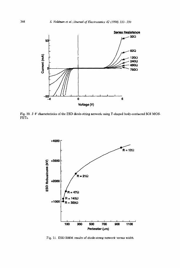
of diode strings in CMOS-on-SOI is that diode series resistance is additive and will degrade ESD results. The diode string can be implemented by connecting the source/drain implants to the input node and the body to the anode of the next diode. The gate of the MOSFET is connected to the body of each diode. Fig. 10 shows I - V characteristics of a five diode-string ESD network for six different size designs. Fig. 11 shows ESD HBM results of the diode-string network versus, width. ESD results show effectiveness as + 3.5 V/~tm of diode width for discharging to the VI~D power grid. The data shown represents an exemplary case of some of the measurements taken on the test structure with an error bar of 100 V. Table 3 shows the relationship between perimeter, diode string series resistance and ESD results using a five diode string ESD network. The ESD network can be modeled as a gated diode with a diode series resistor similar to the diode-string model developed for bulk silicon in the low pnp bipolar limit (diode-resistance dominant mode) [-19]. Experimental results again confirm that the perimeter of the diode structure must be greater than 500 ~m, and with low resistance, to achieve above a 2 kV HBM ESD result. This is similar to ESD results in STI-defined bulk CMOS. Although the demonstration used five diodes in series, as a result of power supply scaling, the number of diodes in series will be reduced as the power supply of semiconductor chips is reduced for 3.3-1.8 V and 2.5-1.8 V interfaces. This allows for considerably smaller structures with lower resist- ance and greater ESD effectiveness.
344 S. Voldman et al./Journal of Electrostatics 42 (1998) 333-350
50
E
+0"
-50 -4
I I
0
Voltage (V)
Series Resistance
/~ 302
60Q
// 1 oo ~ / ~ ~ ' - 4802
' r ~ 7602
I I I
6
Fig. 10. 1-V characteristics of the ESD diode-string network using T-shaped body-contacted SO1 MOS- FETs.
+4000
A > +3000
W W 0 .= m
, Q o +2000 a: (2 (n ill
+1000
2 2
~ = 2 1 2
~ R = 145~ " R = 300Q
1 O0 300 5 700 900 11
Perimeter (~m)
Fig. 11. ESD HBM results of diode-string network versus width.
S. Voldman et al./Journal of Electrostatics 42 (1998) 333-350
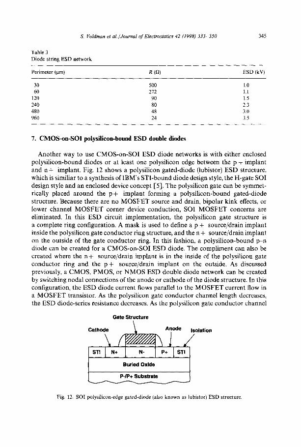
Another way to use CMOS-on-SOI ESD diode networks is with either enclosed polysilicon-bound diodes or at least one polysilicon edge between the p + implant and n + implant. Fig. 12 shows a polysilicon gated-diode (lubistor) ESD structure, which is similiar to a synthesis of IBM's STI-bound diode design style, the H-gate SOl design style and an enclosed device concept [5]. The polysilicon gate can be symmet- rically placed around the p + implant forming a polysilicon-bound gated-diode structure. Because there are no M O S F E T source and drain, bipolar kink effects, or lower channel M O S F E T corner device conduction, SO1 MO S F ET concerns are eliminated. In this ESD circuit implementation, the polysilicon gate structure is a complete ring configuration. A mask is used to define a p + source/drain implant inside the polysilicon gate conductor ring structure, and the n + source/drain implant on the outside of the gate conductor ring. In this fashion, a polysilicon-bound p-n diode can be created for a CMOS-on-SOI ESD diode. The compliment can also be created where the n + source/drain implant is in the inside of the polysilicon gate conductor ring and the p + source/drain implant on the outside. As discussed previously, a CMOS, PMOS, or NMOS ESD double diode network can be created by switching nodal connections of the anode or cathode of the diode structure. In this configuration, the ESD diode current flows parallel to the M O S F E T current flow in a M O S F E T transistor. As the polysilicon gate conductor channel length decreases, the ESD diode-series resistance decreases. As the polysilicon gate conductor channel
Gate Structure
Cathode ~ Anode
STI N+ N- P+ I STI
Buried Oxide
P-/P+ Substrate
Isolation /
Fig. 12. SOl polysilicon-edge gated-diode (also known as lubistor) ESD structure.
346 S. Voldman et al./Journal o f Electrostatics 42 (1998) 333--350
width increases, the ESD diode-series resistance decreases. This design is advantage- ous because current crowding and channel length body-resistance modulation does not occur. Also, the design is simpler, scalable, more compact and mappable directly from bulk STI-defined CMOS.
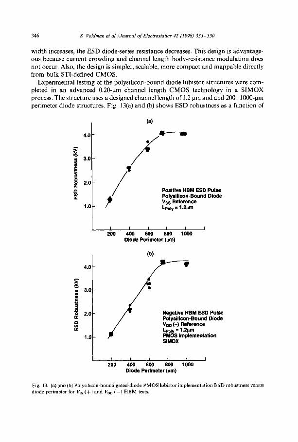
Experimental testing of the polysilicon-bound diode lubistor structures were com- pleted in an advanced 0.20-1am channel length CMOS technology in a SIMOX process. The structure uses a designed channel length of 1.2 pm and and 200-1000-~tm perimeter diode structures. Fig. 13(a) and (b) shows ESD robustness as a function of
a9 c4 4) C
0 n- O C~ W
4.0
3.0
2.0
(a)
m-------~m // Positive HBM ESD Pulse P o l y a i l i c o n - B o u n d D i o d e Vss Reference Lpoly = 1.2v.m
I I I I I I 200 400 600 800 1000
Diode Perimeter (l~m)
v
W (m)
0 rr a uJ
4.0
3.0
2.0
1.0
(b)
Negative HBM ESD Pulse P o l y s i l i c o n - B o u n d D i o d e VDD (-) Reference Lpoly = 1.2V411 PMOS I m p l e m e n t a t i o n S I M O X
I I I I I I 200 400 600 800 1000
D i o d e Perlmeter (pro)
Fig. 13. (a) and (b) Polysilicon-bound gated-diode PMOS lubistor implementation ESD robustness versus diode perimeter for Vss (+) and VDo (--) HBM tests.
S. Voldman et al./Journal of Electrostatics 42 (1998) 333-350 347
Table 4
Lub i s to r ESD
= 1.2 lim) ne twork Vss ( + ) ( length
W i d t h (Ima) E S D (V)
200 1300
400 2600
600 3400 800 4200
1000 4200
Table 5
Lub i s to r
1.2 tim)
E S D ne twork Vss ( - t ( length =
W i d t h (~tm) E S D (V)
200 - 1200
400 - 2200 600 - 3300
800 - 4400 1000 - 4400
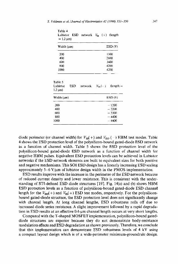
diode perimeter (or channel width) for Vss(+) and VDD (--) HBM test modes. Table 4 shows the ESD protection level of the polysilicon-bound gated-diode ESD network as a function of channel width. Table 5 shows the ESD protection level of the polysilicon-bound gated-diode ESD network as a function of channel width for negative HBM pulses. Equivalent ESD protection levels can be achieved in Lubistor networks if the ESD network elements are built to equivalent sizes for both positive and negative mechanisms. This SO1 ESD design has a linearly increasing ESD scaling approximately 5-6 V/gin of lubistor design width in the PMOS implementation.
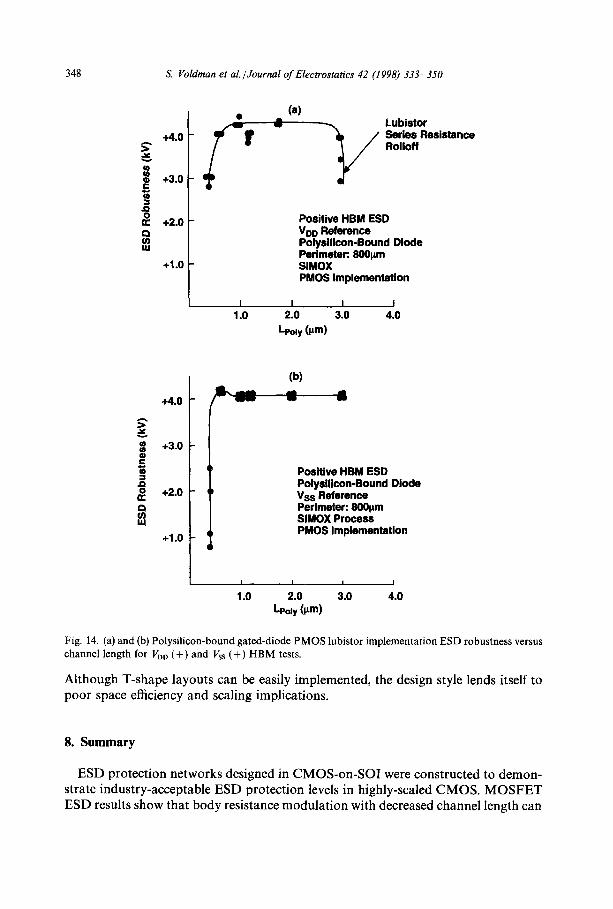
ESD results improve with the increase in the perimeter of the ESD network because of reduced current density and lower resistance. This is consistent with the under- standing of STI-defined ESD diode structures [19]. Fig. 14(a) and (b) shows HBM ESD protection levels as a function of polysilicon-bound gated-diode ESD channel length for the VDD(+) and Vss(+) ESD test modes, respectively. For the polysilicon- bound gated-diode structure, the ESD protection level does not significantly change with channel length. At long channel lengths, ESD robustness rolls off due to increased diode series resistance. A slight improvement followed by a rapid degrada- tion in ESD results at an effective 0.4-gm channel length occurs at very short lengths.
Compared with the T-shaped MOSFET implementation, polysilicon-bound gated- diode structures are superior because they do not demonstrate body-resistance modulation effects and ESD degradation as shown previously. Therefore, we conclude that this implementation can demonstrate ESD robustness levels of 4 kV using a compact layout design which is of a wide-perimeter minimum-groundrule design.
348 S. Voldman et al./Journal of Electrostatics 42 (1998) 333-350
Fig. 14. (a) and (b) Polysilicon-bound gated-diode PMOS lubistor implementation ESD robustness versus channel length for VDo (+) and Vss (+) HBM tests.
Although T-shape layouts can be easily implemented, the design style lends itself to poor space efficiency and scaling implications.
8. Summary
ESD protection networks designed in CMOS-on-SOI were constructed to demon- strate industry-acceptable ESD protection levels in highly-scaled CMOS. MOSFET ESD results show that body resistance modulation with decreased channel length can
S. Voldman et al./Journal of Electrostatics 42 (1998) 333-350 349
degrade negative-pulse ESD robustness. These results also show improvement in negative-mode protection with a grounded gate. ESD-gated diodes were created using both T-shaped MOSFET structures and polysilicon-bound diode structures. ESD results showed that gated diodes constructed from T-shaped MOSFET structures exhibited modulation of the ESD data caused by a change in local body contact resistance with channel length. ESD results also showed that polysilicon-bound gated-diode type lubistor networks are more space efficient and can achieve 4 kV protection levels for a wide-range of channel !ength. ESD results of 5 V/lam of diode width is achieved for Lubistor diode structures in advanced CMOS-on-SOI techno- logy. Lubistor and diode-based ESD networks achieve higher ESD robustness com- pared to MOSFET GGNMOS implementations. Hence, industry-acceptable ESD protection networks can be constructed in highly-scaled CMOS technology without additional masks, processing or highly complex ESD protection schemes.
Acknowledgements
The authors wish to thank B. Davari and P. Cottrell for supporting the experi- mental work and IBM's Advanced Semiconductor Technology Center (ASTC) in East Fishkill, N.Y., and both development teams in IBM Microelectronics Division in Essex Junction, Vermont and East Fishkill, NY.
References
[1] R.H. Dennard, F.H. Gnensslean, H. Yu, V.L. Rideout, E. Bassons, A.R. LeBlanc, Design of ion- implanted M OSFETs with very small physical dimensions, IEEE J. Solid State Circuits SC-9 (1974) 256.
[2] E.A. Vittoz, Low power design: ways to approach the limits, ISSCC Technical Papers, 1994, pp. 14-18.
[3] C. Hu, Low-voltage CMOS device scaling, ISSCC Technical Papers, 1994, pp. 86-87. [4] G.G. Shahidi et al., CMOS scaling in the 0.1 ~tm 1.X volt regime for high performance applications,
IBM J. Res. Dev. 39 (1/2) (1995) 229-245. [5] J.P. Colinge, Silicon-on-Insulator Technology: Materials to VLSI, Kluwer Publications, Dordrecht,
1991. [6] W. Palumbo, M.P. Dugan, Design and characterization of input protection networks for CMOS/SOS
applications, EOS/ESD Symp. Proc., 1986, pp. 182-187. [7] K. Verhaege, G. Groeseneken, J.P. Colinge, H. Maes, The ESD protection of SOl snapback
NMOSFETs: mechanisms and failure modes, EOS/ESD Proc., 1993, pp. 215-219. [8] K. Verhaege, G. Groeseneken, J.P. Colinge, H. Maes, Analysis of snapback in SOl NMOSFETs and
its use for an SOl ESD protection circuit, Proc. IEEE SO1 Conf., 1992, pp. 140-141. [9] K. Verhaege, G. Groeseneken, J.P. Colinge, H. Maes, Double snapback in SO1 NMOSFETs and its
application for SO1 ESD protection, IEEE Electron Device Lett. 14 (7) (1993) 326-328. [10] S. Ramaswamy, P. Raha, E. Rosenbaum, S. Kang, EOS/ESD protection circuit design for deep
submicron SOI technology, EOS/ESD Symp. Proc., 1995, pp. 212-218. [11] Kawai, Method for producing a semiconductor device having a silicon-on-insulator structure, U.S.
Patent 4889 829, 1989. [12] Sun, Fabrication of mixed thin film and bulk semiconductor substrate for integrated circuit applica-
tions, U.S. Patent 5 399 507, 1995.
350 S. Voldman et al./Journal o f Electrostatics 42 (1998) 333-350
1-13] R. Pancholy et al., CMOS/SOS gate protection networks, IEEE Trans. Electron Devices ED-25 (1978) 917-925.
[14] S. Cohen et al., An improved input protection circuit for CMOS/SOS arrays, IEEE Trans. Electron Devices ED-25 (1978) 926-932.
[15] B.T. Ahlport et al., CMOS/SOS LSI input/output protection networks for CMOS/SOS applications, IEEE Trans. Electron Devices ED-25 (1978) 933-938.
[16] M. Chan, S.S. Yuen, Z-J. Ma, K.Y. Hui, P.K. Ko, C. Hu, Comparison of ESD protection capability of SOI and bulk CMOS output buffers, IRPS 1994.
[17] Lu, U.S. Patent #4989057, ESD protection for SO1 circuits, 1991. [18] C. Koburger et al., A half micron CMOS logic generation, IBM J. Res. Dev. 39 (1/2) (1995) 215-229. [19] S. Voldman, G. Gerosa, Mixed voltage interface ESD protection circuits for advanced microproces-
sors in shallow trench and LOCOS isolation CMOS technology, Int. Electron Device Meeting Tech. Digest, Session 10.3.1, 1994, pp. 277-281.