Digital Electronics (2131004) B.E. 3 rd SEMESTER LABORATORY MANUAL 2014 Compiled by Guided by Nitin J. Bathani Dr. K. R. Parmar DEPARTMENT OF ELECTRONICS AND COMMUNICATION ENGINEERING L.D.COLLEGE OF ENGINEERING, AHMEDABAD.
Transcript
Digital Electronics
(2131004)
B.E. 3rd SEMESTER
LABORATORY MANUAL
2014
Compiled by Guided by
Nitin J. Bathani Dr. K. R. Parmar
DEPARTMENT OF ELECTRONICS AND COMMUNICATION ENGINEERING
L.D.COLLEGE OF ENGINEERING, AHMEDABAD.
CERTIFICATE
This is to certify that Mr. /Ms.
_____________________________________________ Roll No.
_______________ and Enrolment no._______________________ Of fourth
semester of B.E____________________ Class has satisfactorily completed
his/her one full semester in “2131004 DIGITAL ELECTRONICS”
satisfactorily in partial fulfilment of Bachelor of Electronics and
communication Engineering degree to be awarded by Gujarat Technological
University.
H.O.D
Faculty – (E&C Department)
Date: - …. /… /…….
L.D. College of Engineering EC Department
Digital Electronics| Compiled By :- Nitin Bathani 1
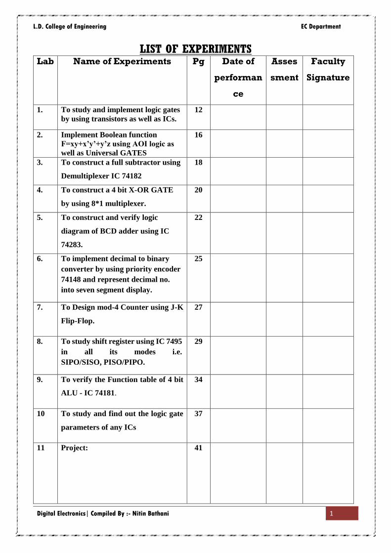
LIST OF EXPERIMENTS Lab Name of Experiments Pg Date of
performan
ce
Asses
sment
Faculty
Signature
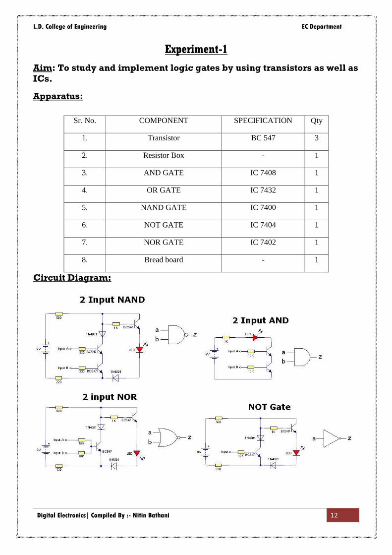
1. To study and implement logic gates
by using transistors as well as ICs.
12
2. Implement Boolean function
F=xy+x’y’+y’z using AOI logic as
well as Universal GATES
16
3. To construct a full subtractor using
Demultiplexer IC 74182
18
4. To construct a 4 bit X-OR GATE
by using 8*1 multiplexer.
20
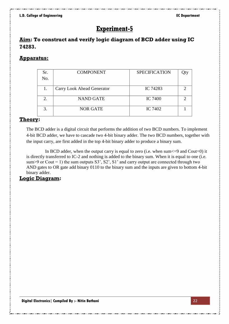
5. To construct and verify logic
diagram of BCD adder using IC
74283.
22
6. To implement decimal to binary
converter by using priority encoder
74148 and represent decimal no.
into seven segment display.
25
7. To Design mod-4 Counter using J-K
Flip-Flop.
27
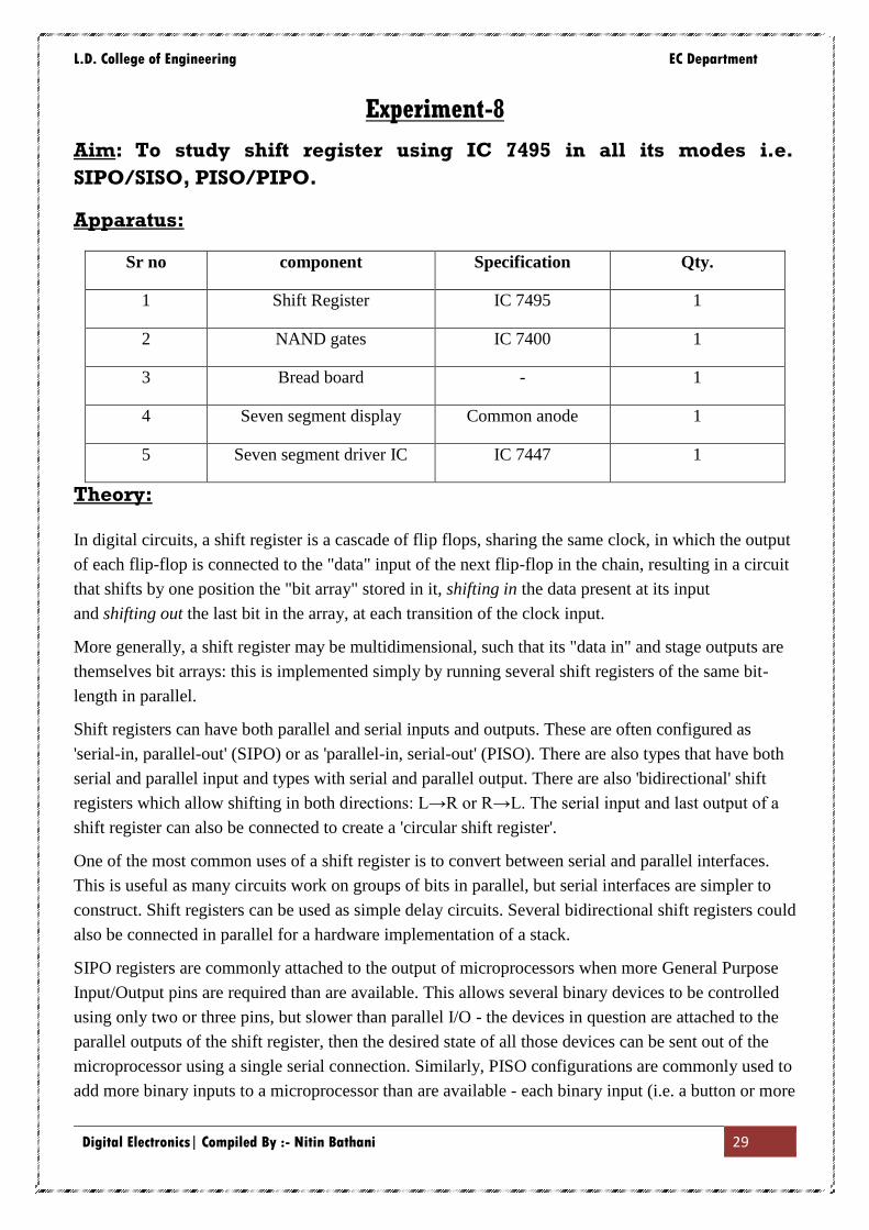
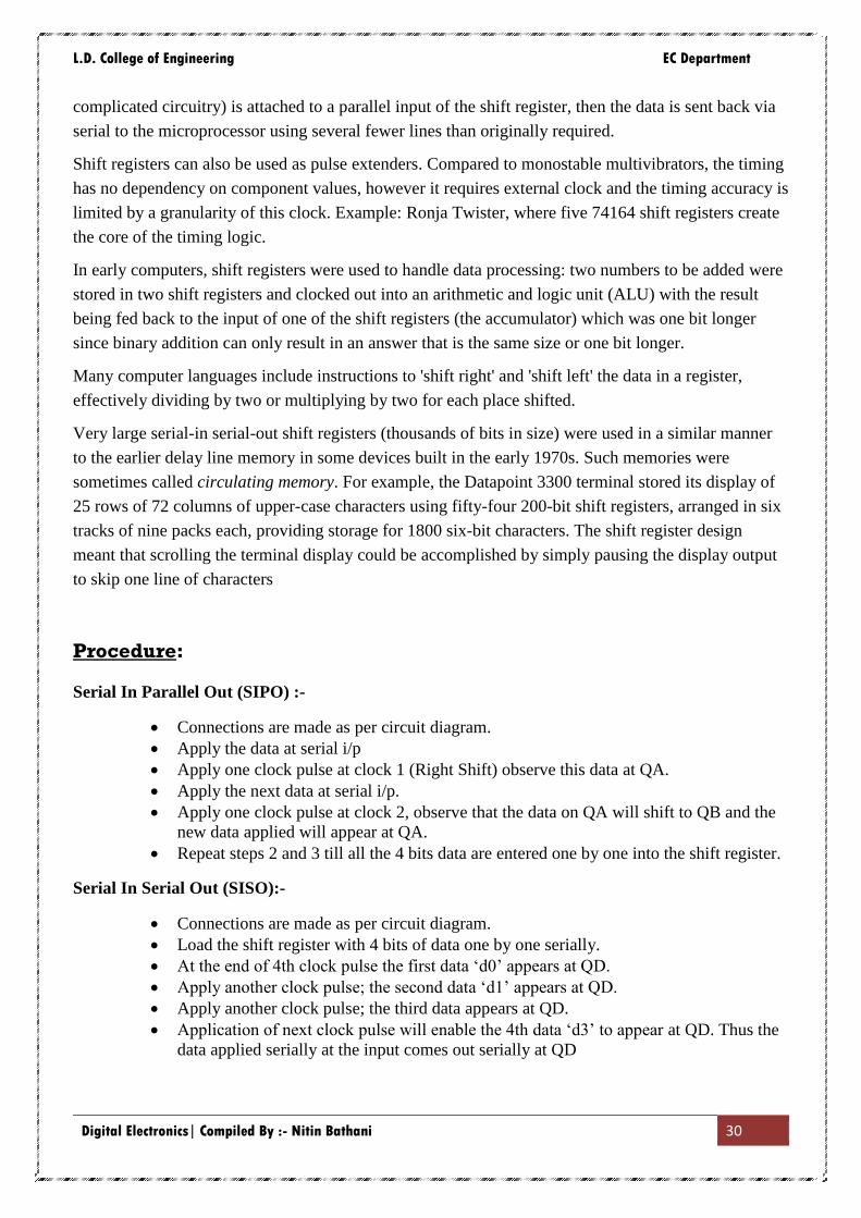
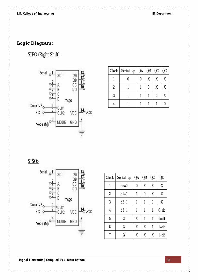
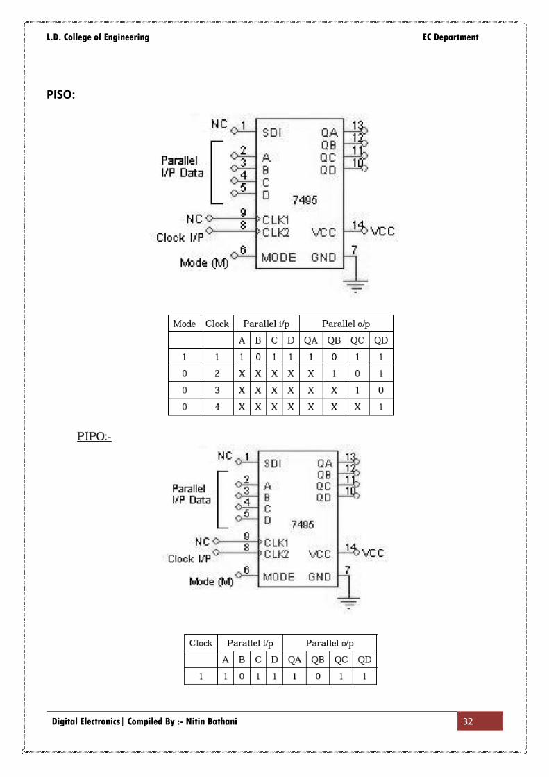
8. To study shift register using IC 7495
in all its modes i.e.
SIPO/SISO, PISO/PIPO.
29
9. To verify the Function table of 4 bit
ALU - IC 74181.
34
10 To study and find out the logic gate
parameters of any ICs
37
11 Project:
41
L.D. College of Engineering EC Department
Digital Electronics| Compiled By :- Nitin Bathani 2
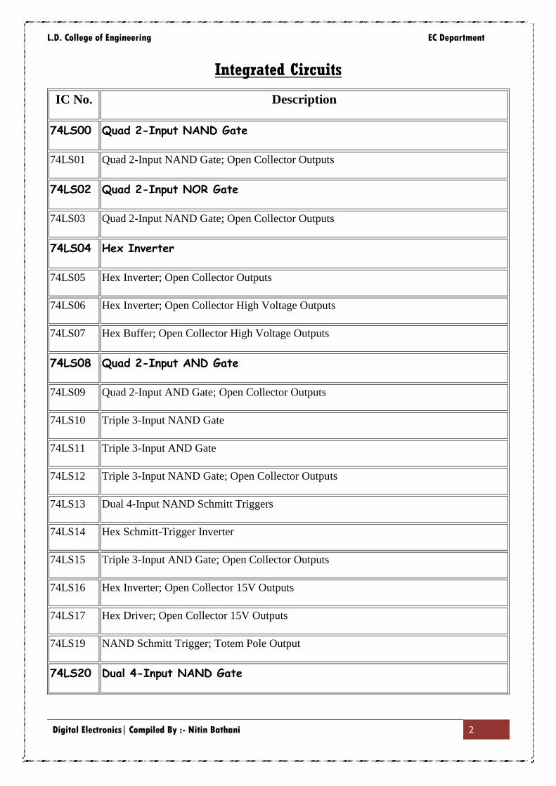
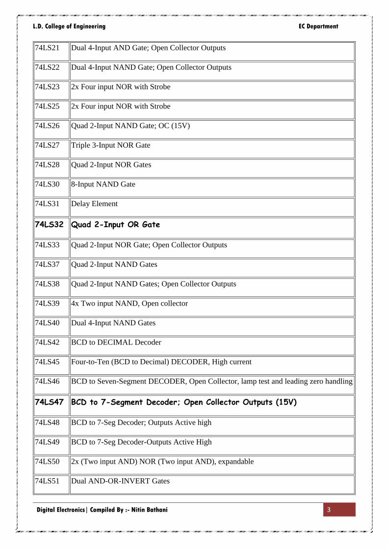
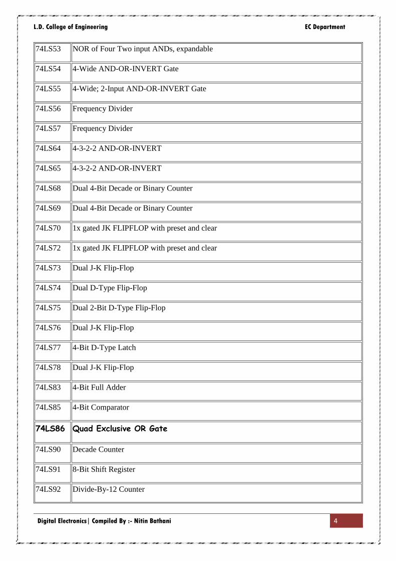
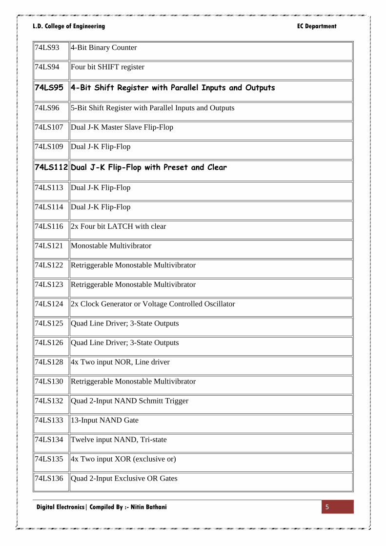
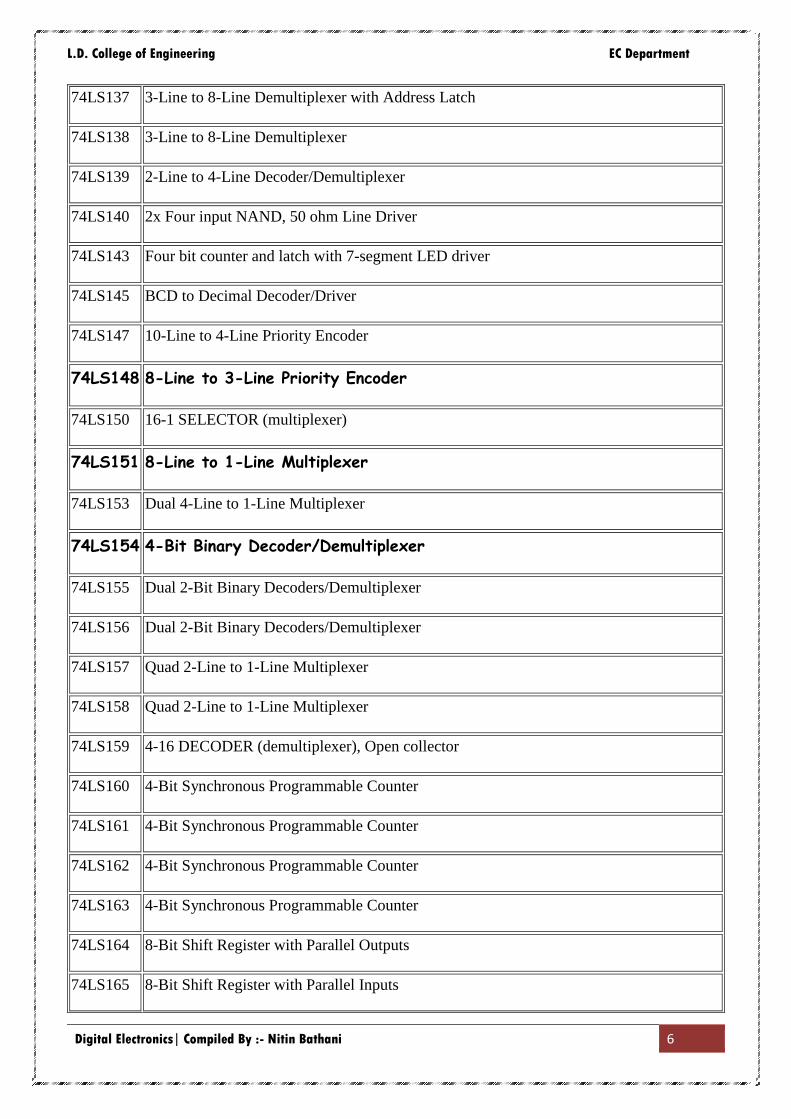
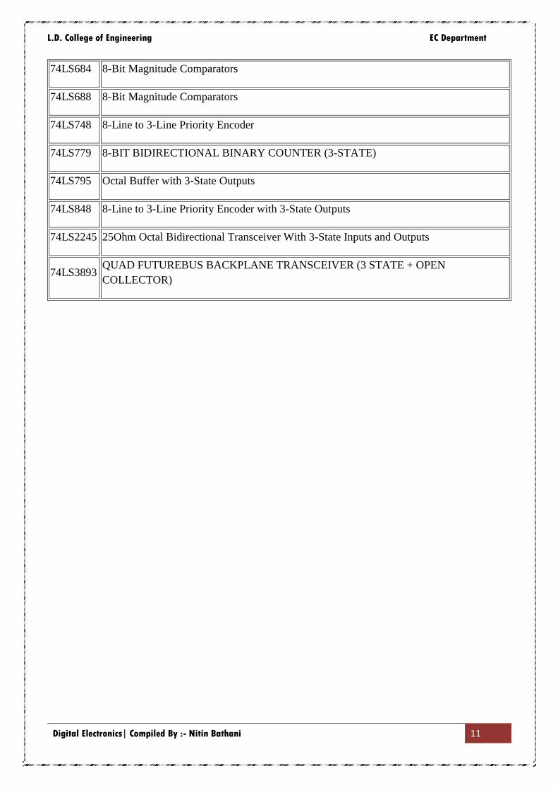
Integrated Circuits
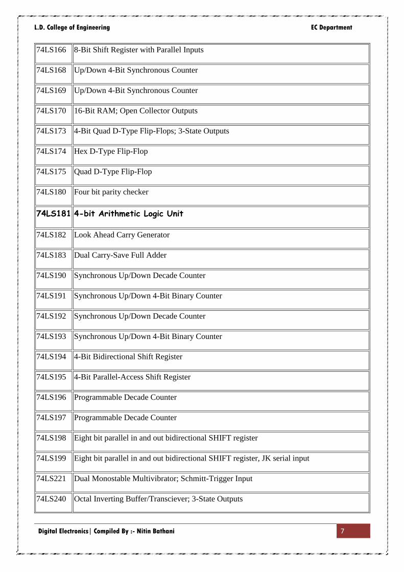
IC No. Description
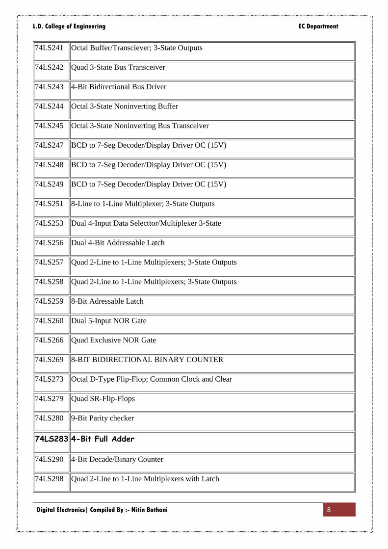
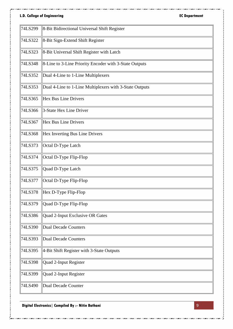
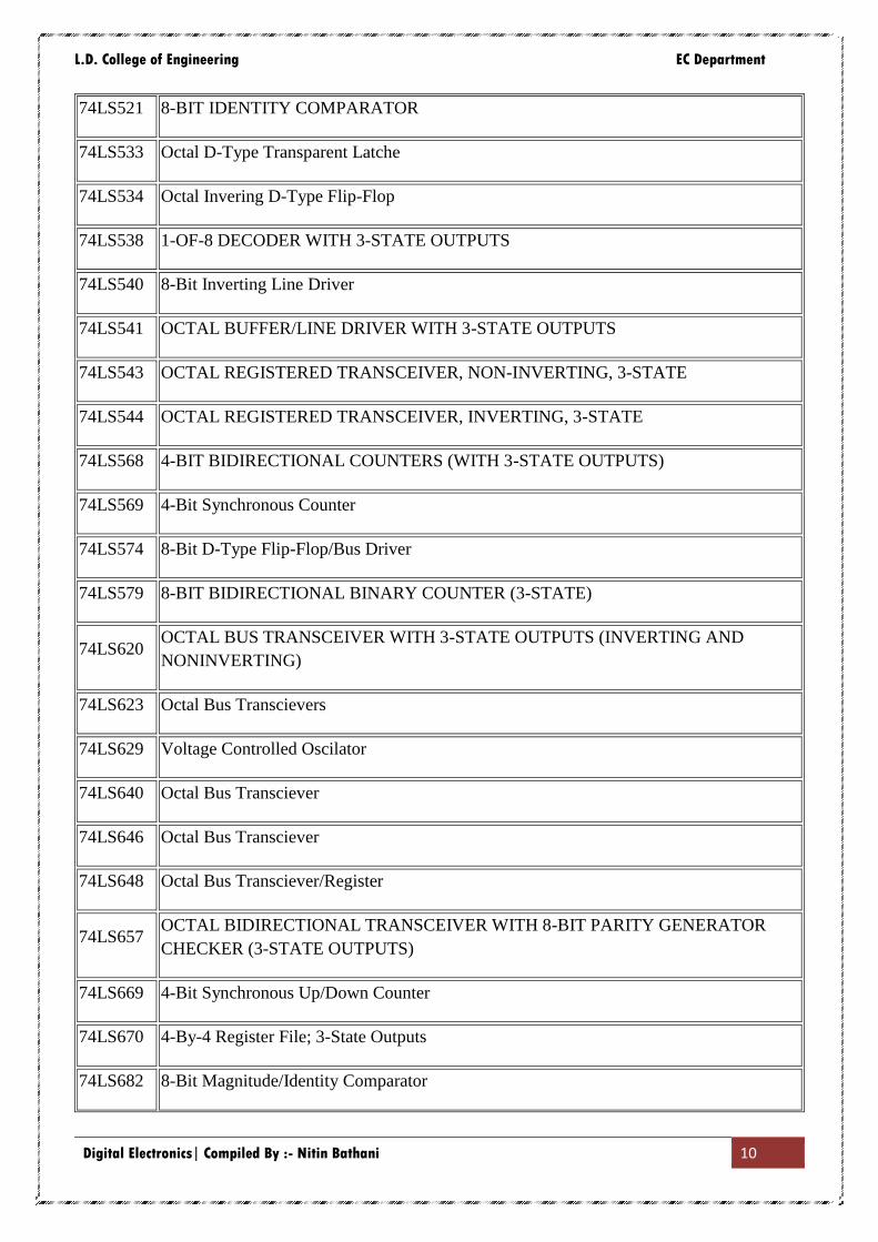
74LS00 Quad 2-Input NAND Gate
74LS01 Quad 2-Input NAND Gate; Open Collector Outputs
74LS02 Quad 2-Input NOR Gate
74LS03 Quad 2-Input NAND Gate; Open Collector Outputs
74LS04 Hex Inverter
74LS05 Hex Inverter; Open Collector Outputs
74LS06 Hex Inverter; Open Collector High Voltage Outputs
74LS07 Hex Buffer; Open Collector High Voltage Outputs
74LS08 Quad 2-Input AND Gate
74LS09 Quad 2-Input AND Gate; Open Collector Outputs
74LS10 Triple 3-Input NAND Gate
74LS11 Triple 3-Input AND Gate
74LS12 Triple 3-Input NAND Gate; Open Collector Outputs
74LS13 Dual 4-Input NAND Schmitt Triggers
74LS14 Hex Schmitt-Trigger Inverter
74LS15 Triple 3-Input AND Gate; Open Collector Outputs
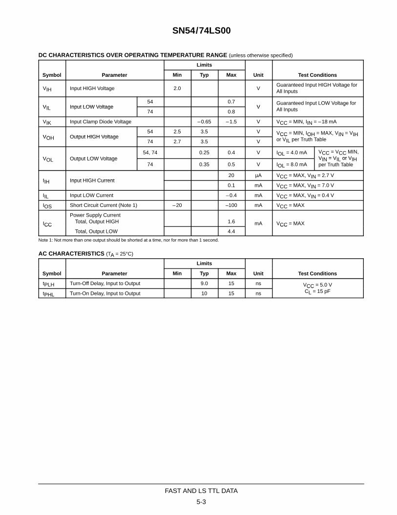
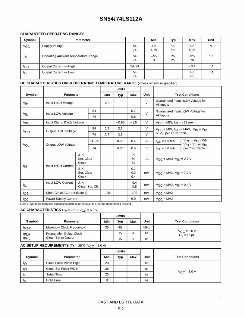
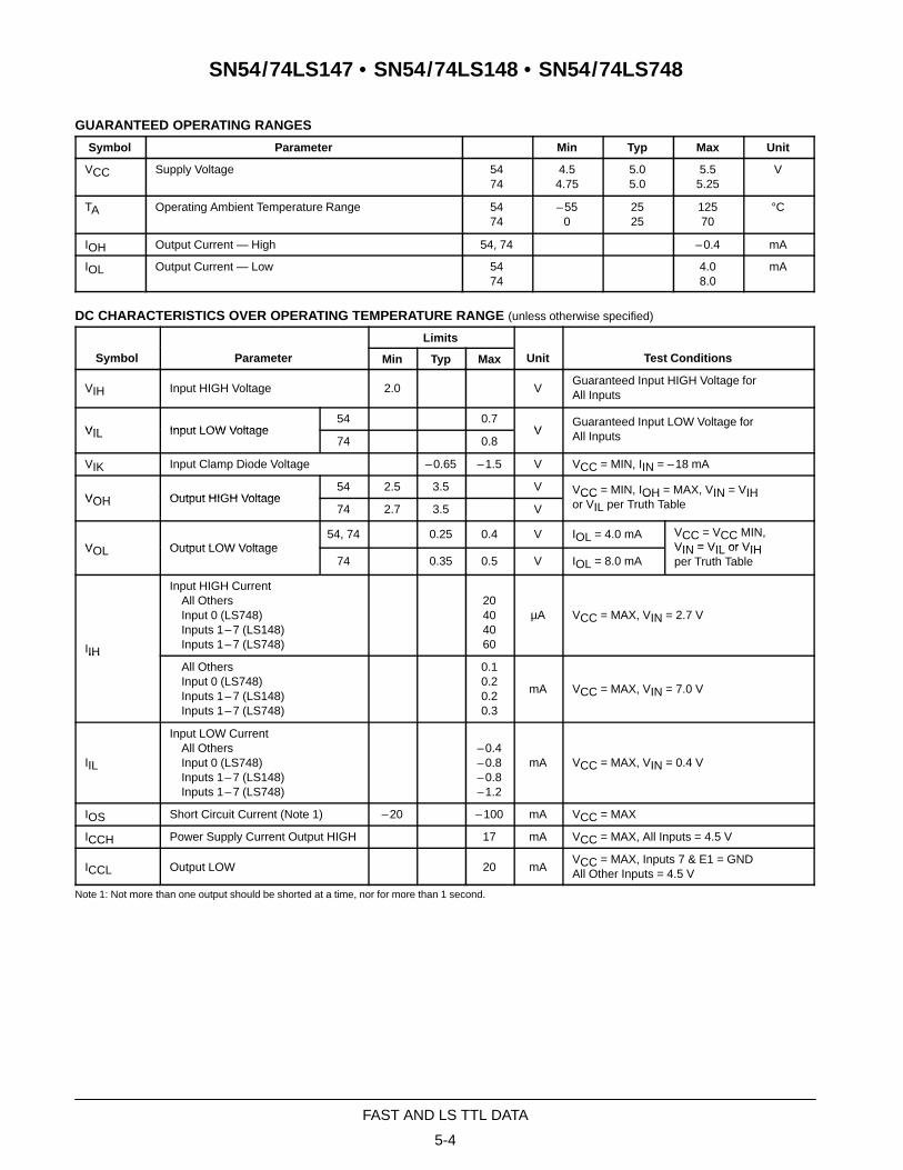
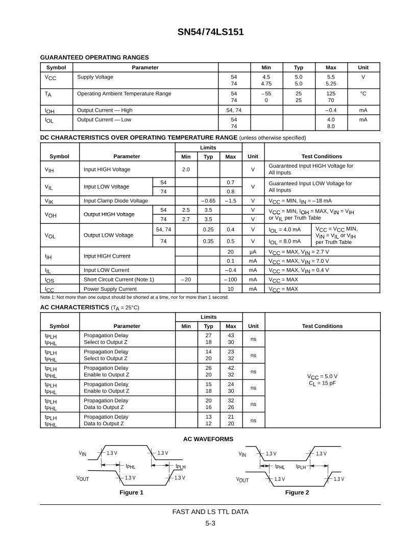
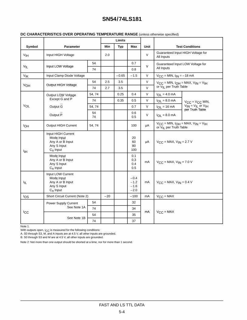
DC CHARACTERISTICS OVER OPERATING TEMPERATURE RANGE (unless otherwise specified)
S b l P
Limits
U i T C di iSymbol Parameter Min Typ Max Unit Test Conditions
VIH Input HIGH Voltage 2.0 VGuaranteed Input HIGH Voltage forAll Inputs
VIL Input LOW Voltage54 0.7
VGuaranteed Input LOW Voltage for
VIL Input LOW Voltage74 0.8
Vp g
All Inputs
VIK Input Clamp Diode Voltage –0.65 –1.5 V VCC = MIN, IIN = –18 mA
VOH Output HIGH Voltage54 2.5 3.5 V VCC = MIN, IOH = MAX, VIN = VIHVOH Output HIGH Voltage74 2.7 3.5 V
CC , OH , IN IHor VIL per Truth Table
VOL Output LOW Voltage54, 74 0.25 0.4 V IOL = 4.0 mA VCC = VCC MIN,
VIN = VIL or VIHVOL Output LOW Voltage74 0.35 0.5 V IOL = 8.0 mA
VIN = VIL or VIHper Truth Table
IIH Input HIGH Current20 µA VCC = MAX, VIN = 2.7 V
IIH Input HIGH Current0.1 mA VCC = MAX, VIN = 7.0 V
IIL Input LOW Current –0.4 mA VCC = MAX, VIN = 0.4 V
IOS Short Circuit Current (Note 1) –20 –100 mA VCC = MAX
ICC
Power Supply CurrentTotal, Output HIGH 1.6 mA VCC = MAXICCTotal, Output LOW 4.4
mA VCC MAX
Note 1: Not more than one output should be shorted at a time, nor for more than 1 second.
AC CHARACTERISTICS (TA = 25°C)
S b l P
Limits
U i T C di iSymbol Parameter Min Typ Max Unit Test Conditions
tPLH Turn-Off Delay, Input to Output 9.0 15 ns VCC = 5.0 V
tPHL Turn-On Delay, Input to Output 10 15 nsCC
CL = 15 pF
5-2
FAST AND LS TTL DATA
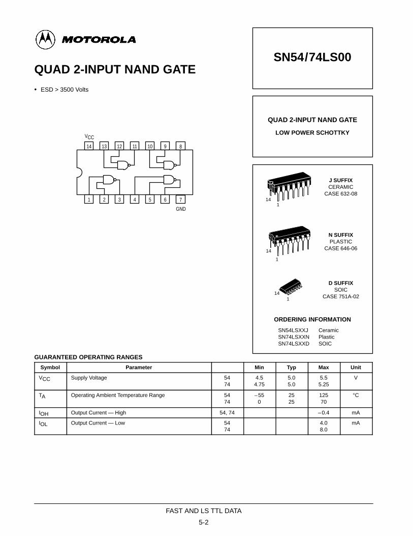
QUAD 2-INPUT NAND GATE
• ESD > 3500 Volts
14 13 12 11 10 9
1 2 3 4 5 6
VCC
8
7
GND
GUARANTEED OPERATING RANGES
Symbol Parameter Min Typ Max Unit
VCC Supply Voltage 5474
4.54.75
5.05.0
5.55.25
V
TA Operating Ambient Temperature Range 5474
–550
2525
12570
°C
IOH Output Current — High 54, 74 –0.4 mA
IOL Output Current — Low 5474
4.08.0
mA
SN54/74LS00
QUAD 2-INPUT NAND GATE
LOW POWER SCHOTTKY
J SUFFIXCERAMIC
CASE 632-08
N SUFFIXPLASTIC
CASE 646-06
141
14
1
ORDERING INFORMATION
SN54LSXXJ CeramicSN74LSXXN PlasticSN74LSXXD SOIC
141
D SUFFIXSOIC
CASE 751A-02
5-3
FAST AND LS TTL DATA
SN54/74LS00
DC CHARACTERISTICS OVER OPERATING TEMPERATURE RANGE (unless otherwise specified)
S b l P
Limits
U i T C di iSymbol Parameter Min Typ Max Unit Test Conditions
VIH Input HIGH Voltage 2.0 VGuaranteed Input HIGH Voltage forAll Inputs
VIL Input LOW Voltage54 0.7
VGuaranteed Input LOW Voltage for
VIL Input LOW Voltage74 0.8
Vp g
All Inputs
VIK Input Clamp Diode Voltage –0.65 –1.5 V VCC = MIN, IIN = –18 mA
VOH Output HIGH Voltage54 2.5 3.5 V VCC = MIN, IOH = MAX, VIN = VIHVOH Output HIGH Voltage74 2.7 3.5 V
CC , OH , IN IHor VIL per Truth Table
VOL Output LOW Voltage54, 74 0.25 0.4 V IOL = 4.0 mA VCC = VCC MIN,
VIN = VIL or VIHVOL Output LOW Voltage74 0.35 0.5 V IOL = 8.0 mA
VIN = VIL or VIHper Truth Table
IIH Input HIGH Current20 µA VCC = MAX, VIN = 2.7 V
IIH Input HIGH Current0.1 mA VCC = MAX, VIN = 7.0 V
IIL Input LOW Current –0.4 mA VCC = MAX, VIN = 0.4 V
IOS Short Circuit Current (Note 1) –20 –100 mA VCC = MAX
ICC
Power Supply CurrentTotal, Output HIGH 1.6 mA VCC = MAXICCTotal, Output LOW 4.4
mA VCC MAX
Note 1: Not more than one output should be shorted at a time, nor for more than 1 second.
AC CHARACTERISTICS (TA = 25°C)
S b l P
Limits
U i T C di iSymbol Parameter Min Typ Max Unit Test Conditions
tPLH Turn-Off Delay, Input to Output 9.0 15 ns VCC = 5.0 V
tPHL Turn-On Delay, Input to Output 10 15 nsCC
CL = 15 pF
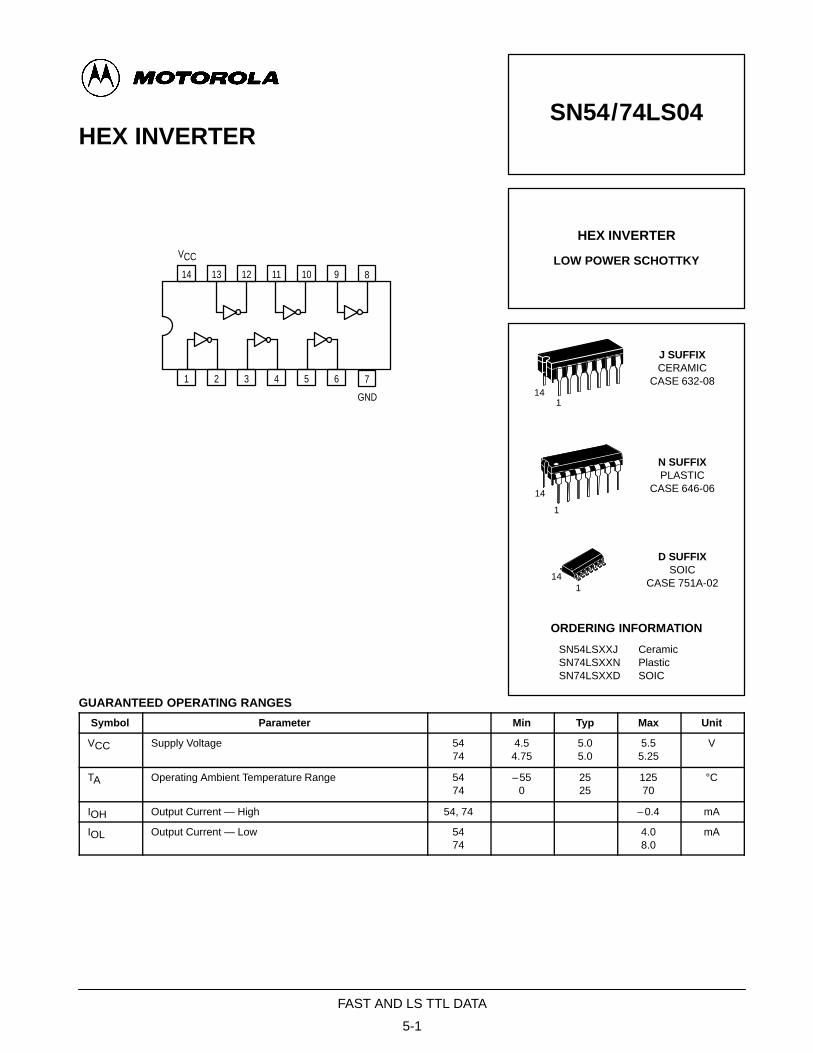
5-1
FAST AND LS TTL DATA
HEX INVERTER
14 13 12 11 10 9
1 2 3 4 5 6
VCC
8
7
GND
GUARANTEED OPERATING RANGES
Symbol Parameter Min Typ Max Unit
VCC Supply Voltage 5474
4.54.75
5.05.0
5.55.25
V
TA Operating Ambient Temperature Range 5474
–550
2525
12570
°C
IOH Output Current — High 54, 74 –0.4 mA
IOL Output Current — Low 5474
4.08.0
mA
SN54/74LS04
HEX INVERTER
LOW POWER SCHOTTKY
J SUFFIXCERAMIC
CASE 632-08
N SUFFIXPLASTIC
CASE 646-06
141
14
1
ORDERING INFORMATION
SN54LSXXJ CeramicSN74LSXXN PlasticSN74LSXXD SOIC
141
D SUFFIXSOIC
CASE 751A-02
5-2
FAST AND LS TTL DATA
SN54/74LS04
DC CHARACTERISTICS OVER OPERATING TEMPERATURE RANGE (unless otherwise specified)
S b l P
Limits
U i T C di iSymbol Parameter Min Typ Max Unit Test Conditions
VIH Input HIGH Voltage 2.0 VGuaranteed Input HIGH Voltage forAll Inputs
VIL Input LOW Voltage54 0.7
VGuaranteed Input LOW Voltage for
VIL Input LOW Voltage74 0.8
Vp g
All Inputs
VIK Input Clamp Diode Voltage –0.65 –1.5 V VCC = MIN, IIN = –18 mA
VOH Output HIGH Voltage54 2.5 3.5 V VCC = MIN, IOH = MAX, VIN = VIHVOH Output HIGH Voltage74 2.7 3.5 V
CC , OH , IN IHor VIL per Truth Table
VOL Output LOW Voltage54, 74 0.25 0.4 V IOL = 4.0 mA VCC = VCC MIN,
VIN = VIL or VIHVOL Output LOW Voltage74 0.35 0.5 V IOL = 8.0 mA
VIN = VIL or VIHper Truth Table
IIH Input HIGH Current20 µA VCC = MAX, VIN = 2.7 V
IIH Input HIGH Current0.1 mA VCC = MAX, VIN = 7.0 V
IIL Input LOW Current –0.4 mA VCC = MAX, VIN = 0.4 V
IOS Short Circuit Current (Note 1) –20 –100 mA VCC = MAX
ICC
Power Supply CurrentTotal, Output HIGH 2.4 mA VCC = MAXICC p
Total, Output LOW 6.6
mA VCC MAX
Note 1: Not more than one output should be shorted at a time, nor for more than 1 second.
AC CHARACTERISTICS (TA = 25°C)
S b l P
Limits
U i T C di iSymbol Parameter Min Typ Max Unit Test Conditions
tPLH Turn-Off Delay, Input to Output 9.0 15 ns VCC = 5.0 V
tPHL Turn-On Delay, Input to Output 10 15 nsCC
CL = 15 pF
5-1
FAST AND LS TTL DATA
QUAD 2-INPUT AND GATE
14 13 12 11 10 9
1 2 3 4 5 6
VCC
8
7
GND
GUARANTEED OPERATING RANGES
Symbol Parameter Min Typ Max Unit
VCC Supply Voltage 5474
4.54.75
5.05.0
5.55.25
V
TA Operating Ambient Temperature Range 5474
–550
2525
12570
°C
IOH Output Current — High 54, 74 –0.4 mA
IOL Output Current — Low 5474
4.08.0
mA
SN54/74LS08
QUAD 2-INPUT AND GATE
LOW POWER SCHOTTKY
J SUFFIXCERAMIC
CASE 632-08
N SUFFIXPLASTIC
CASE 646-06
141
14
1
ORDERING INFORMATION
SN54LSXXJ CeramicSN74LSXXN PlasticSN74LSXXD SOIC
141
D SUFFIXSOIC
CASE 751A-02
5-2
FAST AND LS TTL DATA
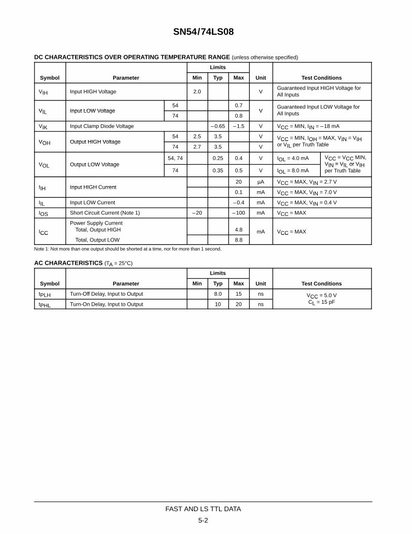
SN54/74LS08
DC CHARACTERISTICS OVER OPERATING TEMPERATURE RANGE (unless otherwise specified)
S b l P
Limits
U i T C di iSymbol Parameter Min Typ Max Unit Test Conditions
VIH Input HIGH Voltage 2.0 VGuaranteed Input HIGH Voltage forAll Inputs
VIL Input LOW Voltage54 0.7
VGuaranteed Input LOW Voltage for
VIL Input LOW Voltage74 0.8
Vp g
All Inputs
VIK Input Clamp Diode Voltage –0.65 –1.5 V VCC = MIN, IIN = –18 mA
VOH Output HIGH Voltage54 2.5 3.5 V VCC = MIN, IOH = MAX, VIN = VIHVOH Output HIGH Voltage74 2.7 3.5 V
CC , OH , IN IHor VIL per Truth Table
VOL Output LOW Voltage54, 74 0.25 0.4 V IOL = 4.0 mA VCC = VCC MIN,
VIN = VIL or VIHVOL Output LOW Voltage74 0.35 0.5 V IOL = 8.0 mA
VIN = VIL or VIHper Truth Table
IIH Input HIGH Current20 µA VCC = MAX, VIN = 2.7 V
IIH Input HIGH Current0.1 mA VCC = MAX, VIN = 7.0 V
IIL Input LOW Current –0.4 mA VCC = MAX, VIN = 0.4 V
IOS Short Circuit Current (Note 1) –20 –100 mA VCC = MAX
ICC
Power Supply CurrentTotal, Output HIGH 4.8 mA VCC = MAXICCTotal, Output LOW 8.8
mA VCC MAX
Note 1: Not more than one output should be shorted at a time, nor for more than 1 second.
AC CHARACTERISTICS (TA = 25°C)
S b l P
Limits
U i T C di iSymbol Parameter Min Typ Max Unit Test Conditions
tPLH Turn-Off Delay, Input to Output 8.0 15 ns VCC = 5.0 V
tPHL Turn-On Delay, Input to Output 10 20 nsCC
CL = 15 pF
5-1
FAST AND LS TTL DATA
DUAL 4-INPUT NAND GATE
14 13 12 11 10 9
1 2 3 4 5 6
VCC
8
7
GND
GUARANTEED OPERATING RANGES
Symbol Parameter Min Typ Max Unit
VCC Supply Voltage 5474
4.54.75
5.05.0
5.55.25
V
TA Operating Ambient Temperature Range 5474
–550
2525
12570
°C
IOH Output Current — High 54, 74 –0.4 mA
IOL Output Current — Low 5474
4.08.0
mA
SN54/74LS20
DUAL 4-INPUT NAND GATE
LOW POWER SCHOTTKY
J SUFFIXCERAMIC
CASE 632-08
N SUFFIXPLASTIC
CASE 646-06
141
14
1
ORDERING INFORMATION
SN54LSXXJ CeramicSN74LSXXN PlasticSN74LSXXD SOIC
141
D SUFFIXSOIC
CASE 751A-02
5-2
FAST AND LS TTL DATA
SN54/74LS20
DC CHARACTERISTICS OVER OPERATING TEMPERATURE RANGE (unless otherwise specified)
S b l P
Limits
U i T C di iSymbol Parameter Min Typ Max Unit Test Conditions
VIH Input HIGH Voltage 2.0 VGuaranteed Input HIGH Voltage forAll Inputs
VIL Input LOW Voltage54 0.7
VGuaranteed Input LOW Voltage for
VIL Input LOW Voltage74 0.8
Vp g
All Inputs
VIK Input Clamp Diode Voltage –0.65 –1.5 V VCC = MIN, IIN = –18 mA
VOH Output HIGH Voltage54 2.5 3.5 V VCC = MIN, IOH = MAX, VIN = VIHVOH Output HIGH Voltage74 2.7 3.5 V
CC , OH , IN IHor VIL per Truth Table
VOL Output LOW Voltage54, 74 0.25 0.4 V IOL = 4.0 mA VCC = VCC MIN,
VIN = VIL or VIHVOL Output LOW Voltage74 0.35 0.5 V IOL = 8.0 mA
VIN = VIL or VIHper Truth Table
IIH Input HIGH Current20 µA VCC = MAX, VIN = 2.7 V
IIH Input HIGH Current0.1 mA VCC = MAX, VIN = 7.0 V
IIL Input LOW Current –0.4 mA VCC = MAX, VIN = 0.4 V
IOS Short Circuit Current (Note 1) –20 –100 mA VCC = MAX
ICC
Power Supply CurrentTotal, Output HIGH 0.8 mA VCC = MAXICC p
Total, Output LOW 2.2
mA VCC MAX
Note 1: Not more than one output should be shorted at a time, nor for more than 1 second.
AC CHARACTERISTICS (TA = 25°C)
S b l P
Limits
U i T C di iSymbol Parameter Min Typ Max Unit Test Conditions
tPLH Turn-Off Delay, Input to Output 9.0 15 ns VCC = 5.0 V
tPHL Turn-On Delay, Input to Output 10 15 nsCC
CL = 15 pF
5-1
FAST AND LS TTL DATA
QUAD 2-INPUT OR GATE
14 13 12 11 10 9
1 2 3 4 5 6
VCC
8
7
GND
GUARANTEED OPERATING RANGES
Symbol Parameter Min Typ Max Unit
VCC Supply Voltage 5474
4.54.75
5.05.0
5.55.25
V
TA Operating Ambient Temperature Range 5474
–550
2525
12570
°C
IOH Output Current — High 54, 74 –0.4 mA
IOL Output Current — Low 5474
4.08.0
mA
SN54/74LS32
QUAD 2-INPUT OR GATE
LOW POWER SCHOTTKY
J SUFFIXCERAMIC
CASE 632-08
N SUFFIXPLASTIC
CASE 646-06
141
14
1
ORDERING INFORMATION
SN54LSXXJ CeramicSN74LSXXN PlasticSN74LSXXD SOIC
141
D SUFFIXSOIC
CASE 751A-02
5-2
FAST AND LS TTL DATA
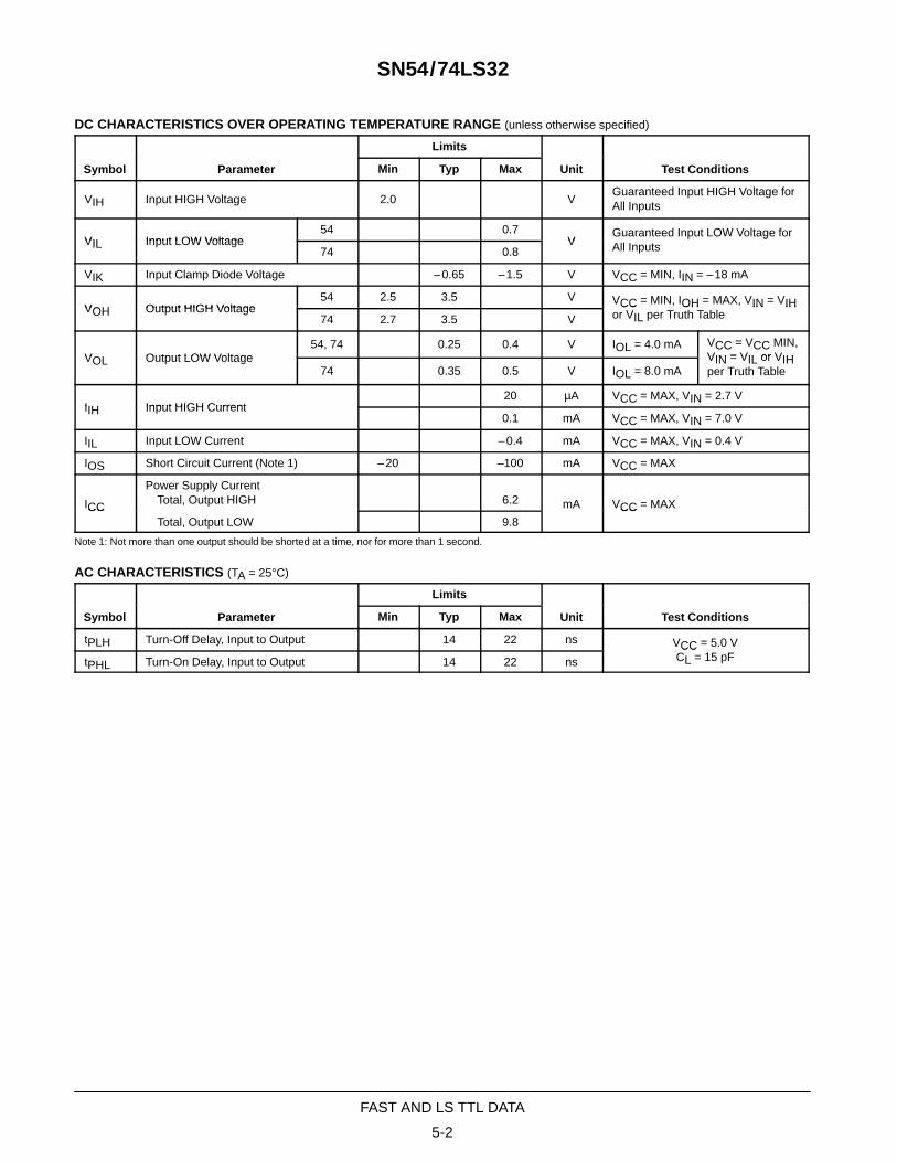
SN54/74LS32
DC CHARACTERISTICS OVER OPERATING TEMPERATURE RANGE (unless otherwise specified)
S b l P
Limits
U i T C di iSymbol Parameter Min Typ Max Unit Test Conditions
VIH Input HIGH Voltage 2.0 VGuaranteed Input HIGH Voltage forAll Inputs
VIL Input LOW Voltage54 0.7
VGuaranteed Input LOW Voltage for
VIL Input LOW Voltage74 0.8
Vp g
All Inputs
VIK Input Clamp Diode Voltage –0.65 –1.5 V VCC = MIN, IIN = –18 mA
VOH Output HIGH Voltage54 2.5 3.5 V VCC = MIN, IOH = MAX, VIN = VIHVOH Output HIGH Voltage74 2.7 3.5 V
CC , OH , IN IHor VIL per Truth Table
VOL Output LOW Voltage54, 74 0.25 0.4 V IOL = 4.0 mA VCC = VCC MIN,
VIN = VIL or VIHVOL Output LOW Voltage74 0.35 0.5 V IOL = 8.0 mA
VIN = VIL or VIHper Truth Table
IIH Input HIGH Current20 µA VCC = MAX, VIN = 2.7 V
IIH Input HIGH Current0.1 mA VCC = MAX, VIN = 7.0 V
IIL Input LOW Current –0.4 mA VCC = MAX, VIN = 0.4 V
IOS Short Circuit Current (Note 1) –20 –100 mA VCC = MAX
ICC
Power Supply CurrentTotal, Output HIGH 6.2 mA VCC = MAXICCTotal, Output LOW 9.8
mA VCC MAX
Note 1: Not more than one output should be shorted at a time, nor for more than 1 second.
AC CHARACTERISTICS (TA = 25°C)
S b l P
Limits
U i T C di iSymbol Parameter Min Typ Max Unit Test Conditions
tPLH Turn-Off Delay, Input to Output 14 22 ns VCC = 5.0 V
tPHL Turn-On Delay, Input to Output 14 22 nsCC
CL = 15 pF
5-1
FAST AND LS TTL DATA
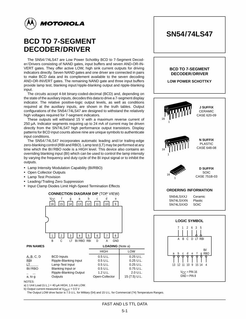
BCD TO 7-SEGMENTDECODER/DRIVER
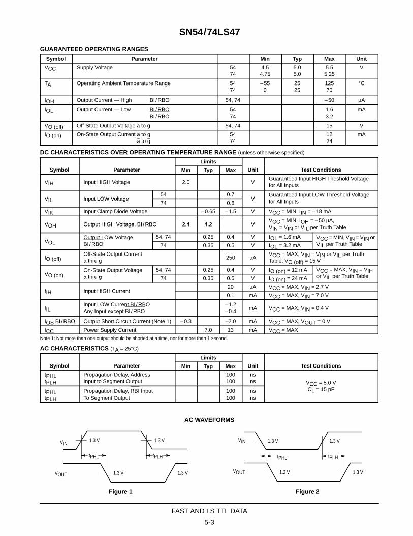
The SN54/74LS47 are Low Power Schottky BCD to 7-Segment Decod-er /Drivers consisting of NAND gates, input buffers and seven AND-OR-IN-VERT gates. They offer active LOW, high sink current outputs for drivingindicators directly. Seven NAND gates and one driver are connected in pairsto make BCD data and its complement available to the seven decodingAND-OR-INVERT gates. The remaining NAND gate and three input buffersprovide lamp test, blanking input / ripple-blanking output and ripple-blankinginput.
The circuits accept 4-bit binary-coded-decimal (BCD) and, depending onthe state of the auxiliary inputs, decodes this data to drive a 7-segment displayindicator. The relative positive-logic output levels, as well as conditionsrequired at the auxiliary inputs, are shown in the truth tables. Outputconfigurations of the SN54/74LS47 are designed to withstand the relativelyhigh voltages required for 7-segment indicators.
These outputs will withstand 15 V with a maximum reverse current of250 µA. Indicator segments requiring up to 24 mA of current may be drivendirectly from the SN74LS47 high performance output transistors. Displaypatterns for BCD input counts above nine are unique symbols to authenticateinput conditions.
The SN54/74LS47 incorporates automatic leading and/or trailing-edgezero-blanking control (RBI and RBO). Lamp test (LT) may be performed at anytime which the BI /RBO node is a HIGH level. This device also contains anoverriding blanking input (BI) which can be used to control the lamp intensityby varying the frequency and duty cycle of the BI input signal or to inhibit theoutputs.
• Lamp Intensity Modulation Capability (BI/RBO)• Open Collector Outputs• Lamp Test Provision• Leading/Trailing Zero Suppression• Input Clamp Diodes Limit High-Speed Termination Effects
NOTES:a) 1 Unit Load (U.L.) = 40 µA HIGH, 1.6 mA LOW.b) Output current measured at VOUT = 0.5 V
The Output LOW drive factor is 7.5 U.L. for Military (54) and 15 U.L. for Commercial (74) Temperature Ranges.
SN54/74LS47
BCD TO 7-SEGMENTDECODER/DRIVER
LOW POWER SCHOTTKY
J SUFFIXCERAMIC
CASE 620-09
N SUFFIXPLASTIC
CASE 648-08
161
16
1
ORDERING INFORMATION
SN54LSXXJ CeramicSN74LSXXN PlasticSN74LSXXD SOIC
161
D SUFFIXSOIC
CASE 751B-03
LOGIC SYMBOL
VCC = PIN 16GND = PIN 8
7 1 2 6 3 5
13 12 11 10 9 15 14 4
A B C D LT RBI
a b c d e f gBI/RBO
INPUTS OUTPUTS
TRUTH TABLE
5-2
FAST AND LS TTL DATA
SN54/74LS47
14 15
LOGIC DIAGRAM
NUMERICAL DESIGNATIONS — RESULTANT DISPLAYS
0 1 2 3 4 5 6 7 8 9 10 11 12 13
INPUT
BLANKING INPUT ORRIPPLE-BLANKINGOUTPUT
RIPPLE-BLANKINGINPUT
LAMP-TESTINPUT
A
B
C
D
a a
b b
c c
d d
e e
f f
g g
OUTPUT
DECIMALOR
FUNCTIONLT RBI D C B A BI/RBO a b c d e f g NOTE
0 H H L L L L H L L L L L L H A
1 H X L L L H H H L L H H H H A
2 H X L L H L H L L H L L H L
3 H X L L H H H L L L L H H L
4 H X L H L L H H L L H H L L
5 H X L H L H H L H L L H L L
6 H X L H H L H H H L L L L L
7 H X L H H H H L L L H H H H
8 H X H L L L H L L L L L L L
9 H X H L L H H L L L H H L L
10 H X H L H L H H H H L L H L
11 H X H L H H H H H L L H H L
12 H X H H L L H H L H H H L L
13 H X H H L H H L H H L H L L
14 H X H H H L H H H H L L L L
15 H X H H H H H H H H H H H H
BI X X X X X X L H H H H H H H B
RBI H L L L L L L H H H H H H H C
LT L X X X X X H L L L L L L L D
H = HIGH Voltage Level L = LOW Voltage Level X = Immaterial
NOTES:(A) BI/RBO is wire-AND logic serving as blanking Input (BI) and/or ripple-blanking output (RBO). The blanking out (BI) must be open or held
at a HIGH level when output functions 0 through 15 are desired, and ripple-blanking input (RBI) must be open or at a HIGH level if blankingof a decimal 0 is not desired. X = input may be HIGH or LOW.
(B) When a LOW level is applied to the blanking input (forced condition) all segment outputs go to a LOW level regardless of the state ofany other input condition.
(C) When ripple-blanking input (RBI) and inputs A, B, C, and D are at LOW level, with the lamp test input at HIGH level, all segment outputsgo to a HIGH level and the ripple-blanking output (RBO) goes to a LOW level (response condition).
(D) When the blanking input/ripple-blanking output (BI/RBO) is open or held at a HIGH level, and a LOW level is applied to lamp test input,all segment outputs go to a LOW level.
5-3
FAST AND LS TTL DATA
SN54/74LS47
GUARANTEED OPERATING RANGES
Symbol Parameter Min Typ Max Unit
VCC Supply Voltage 5474
4.54.75
5.05.0
5.55.25
V
TA Operating Ambient Temperature Range 5474
–550
2525
12570
°C
IOH Output Current — High BI /RBO 54, 74 –50 µA
IOL Output Current — Low BI /RBOBI /RBO
5474
1.63.2
mA
VO (off) Off-State Output Voltage a to g 54, 74 15 V
IO (on) On-State Output Current a to gOn-State Output Current a to g
5474
1224
mA
DC CHARACTERISTICS OVER OPERATING TEMPERATURE RANGE (unless otherwise specified)
S b l P
Limits
U i T C di iSymbol Parameter Min Typ Max Unit Test Conditions
VIH Input HIGH Voltage 2.0 VGuaranteed Input HIGH Theshold Voltagefor All Inputs
VIL Input LOW Voltage54 0.7
VGuaranteed Input LOW Threshold Voltage
VIL Input LOW Voltage74 0.8
Vp g
for All Inputs
VIK Input Clamp Diode Voltage –0.65 –1.5 V VCC = MIN, IIN = –18 mA
VOH Output HIGH Voltage BI /RBO 2 4 4 2 VVCC = MIN, IOH = –50 µA,
VOH Output HIGH Voltage, BI /RBO 2.4 4.2 V CC , OH µ ,VIN = VIN or VIL per Truth Table
VOLOutput LOW Voltage 54, 74 0.25 0.4 V IOL = 1.6 mA VCC = MIN, VIN = VIN or
VOLp g
BI /RBO 74 0.35 0.5 V IOL = 3.2 mACC , IN IN
VIL per Truth Table
IO (off)Off-State Output Currenta thru g 250 µA
VCC = MAX, VIN = VIN or VIL per TruthTable, VO (off) = 15 V
VO (on)On-State Output Voltage 54, 74 0.25 0.4 V IO (on) = 12 mA VCC = MAX, VIN = VIH
V T th T blVO (on)p g
a thru g 74 0.35 0.5 V IO (on) = 24 mACC IN IH
or VIL per Truth Table
IIH Input HIGH Current20 µA VCC = MAX, VIN = 2.7 V
IIH Input HIGH Current0.1 mA VCC = MAX, VIN = 7.0 V
IILInput LOW Current BI /RBOAny Input except BI /RBO
–1.2–0.4 mA VCC = MAX, VIN = 0.4 V
IOS BI /RBO Output Short Circuit Current (Note 1) –0.3 –2.0 mA VCC = MAX, VOUT = 0 V
ICC Power Supply Current 7.0 13 mA VCC = MAX
Note 1: Not more than one output should be shorted at a time, nor for more than 1 second.
AC CHARACTERISTICS (TA = 25°C)
S b l P
Limits
U i T C di iSymbol Parameter Min Typ Max Unit Test Conditions
tPHLtPLH
Propagation Delay, AddressInput to Segment Output
100100
nsns VCC = 5.0 V
tPHLtPLH
Propagation Delay, RBI InputTo Segment Output
100100
nsns
VCC 5.0 VCL = 15 pF
AC WAVEFORMS
VIN
VOUT
1.3 V 1.3 V
1.3 V 1.3 V
tPHL tPLH
Figure 1 Figure 2
1.3 V 1.3 V
1.3 V1.3 V
tPLHtPHL
VIN
VOUT
5-1
FAST AND LS TTL DATA
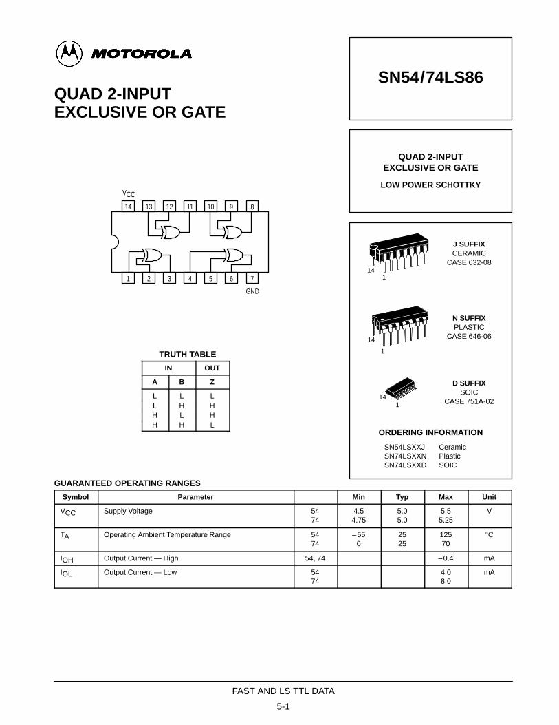
QUAD 2-INPUTEXCLUSIVE OR GATE
14 13 12 11 10 9
1 2 3 4 5 6
VCC
8
7
GND
TRUTH TABLE
IN OUT
A B Z
L L LL H HH L HH H L
GUARANTEED OPERATING RANGES
Symbol Parameter Min Typ Max Unit
VCC Supply Voltage 5474
4.54.75
5.05.0
5.55.25
V
TA Operating Ambient Temperature Range 5474
–550
2525
12570
°C
IOH Output Current — High 54, 74 –0.4 mA
IOL Output Current — Low 5474
4.08.0
mA
SN54/74LS86
QUAD 2-INPUTEXCLUSIVE OR GATE
LOW POWER SCHOTTKY
J SUFFIXCERAMIC
CASE 632-08
N SUFFIXPLASTIC
CASE 646-06
141
14
1
ORDERING INFORMATION
SN54LSXXJ CeramicSN74LSXXN PlasticSN74LSXXD SOIC
141
D SUFFIXSOIC
CASE 751A-02
5-2
FAST AND LS TTL DATA
SN54/74LS86
DC CHARACTERISTICS OVER OPERATING TEMPERATURE RANGE (unless otherwise specified)
S b l P
Limits
U i T C di iSymbol Parameter Min Typ Max Unit Test Conditions
VIH Input HIGH Voltage 2.0 VGuaranteed Input HIGH Voltage forAll Inputs
VIL Input LOW Voltage54 0.7
VGuaranteed Input LOW Voltage for
VIL Input LOW Voltage74 0.8
Vp g
All Inputs
VIK Input Clamp Diode Voltage –0.65 –1.5 V VCC = MIN, IIN = –18 mA
VOH Output HIGH Voltage54 2.5 3.5 V VCC = MIN, IOH = MAX, VIN = VIHVOH Output HIGH Voltage74 2.7 3.5 V
CC , OH , IN IHor VIL per Truth Table
VOL Output LOW Voltage54, 74 0.25 0.4 V IOL = 4.0 mA VCC = VCC MIN,
VIN = VIL or VIHVOL Output LOW Voltage74 0.35 0.5 V IOL = 8.0 mA
VIN = VIL or VIHper Truth Table
IIH Input HIGH Current40 µA VCC = MAX, VIN = 2.7 V
IIH Input HIGH Current0.2 mA VCC = MAX, VIN = 7.0 V
IIL Input LOW Current –0.8 mA VCC = MAX, VIN = 0.4 V
IOS Short Circuit Current (Note 1) –20 –100 mA VCC = MAX
ICC Power Supply Current 10 mA VCC = MAX
Note 1: Not more than one output should be shorted at a time, nor for more than 1 second.
AC CHARACTERISTICS (TA = 25°C)
S b l P
Limits
U i T C di iSymbol Parameter Min Typ Max Unit Test Conditions
tPLHtPHL
Propagation Delay,Other Input LOW
1210
2317 ns
VCC = 5.0 V
tPLHtPHL
Propagation Delay,Other Input HIGH
2013
3022 ns
CCCL = 15 pF
5-1
FAST AND LS TTL DATA
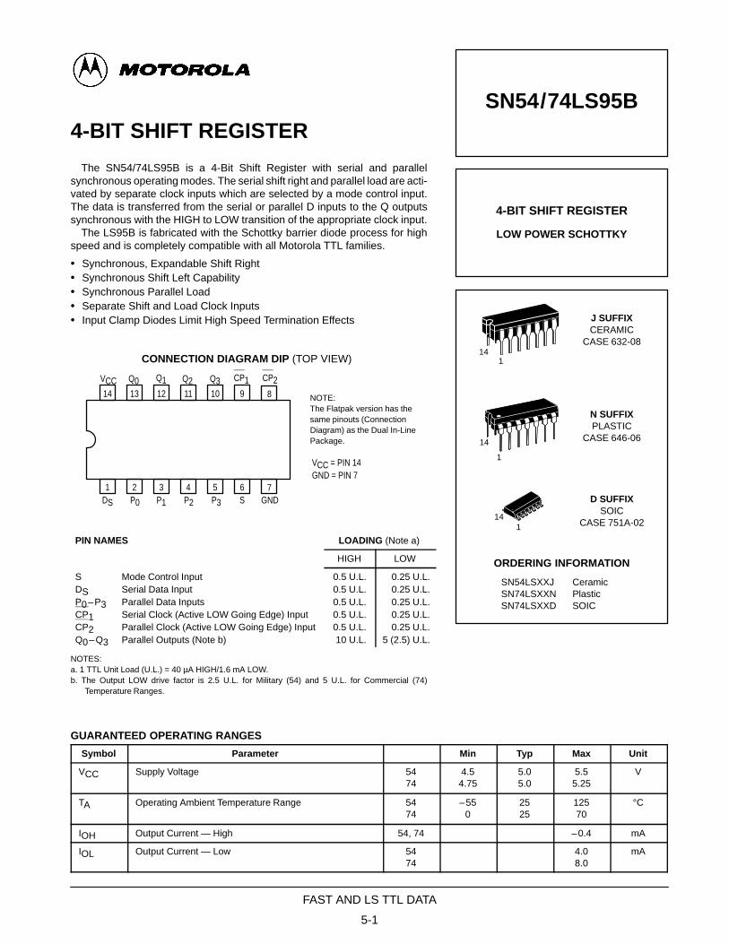
4-BIT SHIFT REGISTER
The SN54/74LS95B is a 4-Bit Shift Register with serial and parallelsynchronous operating modes. The serial shift right and parallel load are acti-vated by separate clock inputs which are selected by a mode control input.The data is transferred from the serial or parallel D inputs to the Q outputssynchronous with the HIGH to LOW transition of the appropriate clock input.
The LS95B is fabricated with the Schottky barrier diode process for highspeed and is completely compatible with all Motorola TTL families.
• Synchronous, Expandable Shift Right• Synchronous Shift Left Capability• Synchronous Parallel Load• Separate Shift and Load Clock Inputs• Input Clamp Diodes Limit High Speed Termination Effects
NOTE:The Flatpak version has thesame pinouts (ConnectionDiagram) as the Dual In-LinePackage.
CONNECTION DIAGRAM DIP (TOP VIEW)
VCC = PIN 14GND = PIN 7
14 13 12 11 10 9
1 2 3 4 5 6
8
7
VCC Q0 Q1 Q2 Q3 CP1 CP2
DS P0 P1 P2 P3 S GND
PIN NAMES LOADING (Note a)
HIGH LOW
S Mode Control Input 0.5 U.L. 0.25 U.L.DS Serial Data Input 0.5 U.L. 0.25 U.L.P0–P3 Parallel Data Inputs 0.5 U.L. 0.25 U.L.CP1 Serial Clock (Active LOW Going Edge) Input 0.5 U.L. 0.25 U.L.CP2 Parallel Clock (Active LOW Going Edge) Input 0.5 U.L. 0.25 U.L.Q0–Q3 Parallel Outputs (Note b) 10 U.L. 5 (2.5) U.L.
NOTES:a. 1 TTL Unit Load (U.L.) = 40 µA HIGH/1.6 mA LOW.b. The Output LOW drive factor is 2.5 U.L. for Military (54) and 5 U.L. for Commercial (74)
Temperature Ranges.
GUARANTEED OPERATING RANGES
Symbol Parameter Min Typ Max Unit
VCC Supply Voltage 5474
4.54.75
5.05.0
5.55.25
V
TA Operating Ambient Temperature Range 5474
–550
2525
12570
°C
IOH Output Current — High 54, 74 –0.4 mA
IOL Output Current — Low 5474
4.08.0
mA
SN54/74LS95B
4-BIT SHIFT REGISTER
LOW POWER SCHOTTKY
J SUFFIXCERAMIC
CASE 632-08
N SUFFIXPLASTIC
CASE 646-06
141
14
1
ORDERING INFORMATION
SN54LSXXJ CeramicSN74LSXXN PlasticSN74LSXXD SOIC
141
D SUFFIXSOIC
CASE 751A-02
5-2
FAST AND LS TTL DATA
SN54/74LS95B
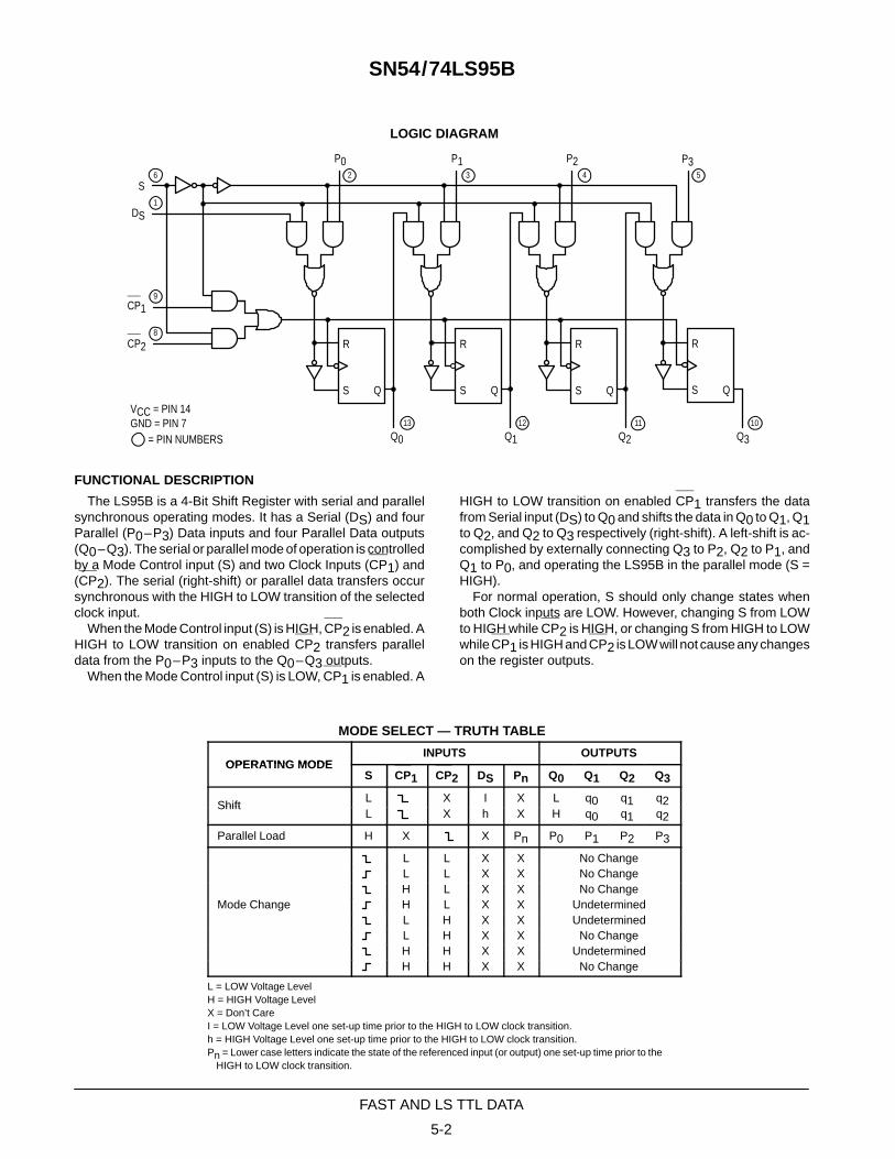
LOGIC DIAGRAM
Q0 Q1 Q2 Q3
S
DS
CP1
CP2
P0 P2 P3
R
S Q
P1
R
S Q
R
S Q
R
S Q
VCC = PIN 14GND = PIN 7
= PIN NUMBERS
6
1
2 3
8
4 5
9
1112 1013
FUNCTIONAL DESCRIPTION
The LS95B is a 4-Bit Shift Register with serial and parallelsynchronous operating modes. It has a Serial (DS) and fourParallel (P0–P3) Data inputs and four Parallel Data outputs(Q0–Q3). The serial or parallel mode of operation is controlledby a Mode Control input (S) and two Clock Inputs (CP1) and(CP2). The serial (right-shift) or parallel data transfers occursynchronous with the HIGH to LOW transition of the selectedclock input.
When the Mode Control input (S) is HIGH, CP2 is enabled. AHIGH to LOW transition on enabled CP2 transfers paralleldata from the P0–P3 inputs to the Q0–Q3 outputs.
When the Mode Control input (S) is LOW, CP1 is enabled. A
HIGH to LOW transition on enabled CP1 transfers the datafrom Serial input (DS) to Q0 and shifts the data in Q0 to Q1, Q1to Q2, and Q2 to Q3 respectively (right-shift). A left-shift is ac-complished by externally connecting Q3 to P2, Q2 to P1, andQ1 to P0, and operating the LS95B in the parallel mode (S =HIGH).
For normal operation, S should only change states whenboth Clock inputs are LOW. However, changing S from LOWto HIGH while CP2 is HIGH, or changing S from HIGH to LOWwhile CP1 is HIGH and CP2 is LOW will not cause any changeson the register outputs.
MODE SELECT — TRUTH TABLE
OPERATING MODEINPUTS OUTPUTS
OPERATING MODES CP1 CP2 DS Pn Q0 Q1 Q2 Q3
ShiftL X I X L q0 q1 q2ShiftL X h X H q0 q1 q2
Parallel Load H X X Pn P0 P1 P2 P3
L L X X No ChangeL L X X No ChangeH L X X No Change
Mode Change H L X X UndeterminedL H X X UndeterminedL H X X No ChangeH H X X UndeterminedH H X X No Change
L = LOW Voltage LevelH = HIGH Voltage LevelX = Don’t CareI = LOW Voltage Level one set-up time prior to the HIGH to LOW clock transition.h = HIGH Voltage Level one set-up time prior to the HIGH to LOW clock transition.Pn = Lower case letters indicate the state of the referenced input (or output) one set-up time prior to the Pn= HIGH to LOW clock transition.
5-3
FAST AND LS TTL DATA
SN54/74LS95B
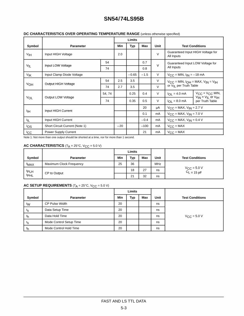
DC CHARACTERISTICS OVER OPERATING TEMPERATURE RANGE (unless otherwise specified)
S b l P
Limits
U i T C di iSymbol Parameter Min Typ Max Unit Test Conditions
VIH Input HIGH Voltage 2.0 VGuaranteed Input HIGH Voltage forAll Inputs
VIL Input LOW Voltage54 0.7
VGuaranteed Input LOW Voltage for
VIL Input LOW Voltage74 0.8
Vp g
All Inputs
VIK Input Clamp Diode Voltage –0.65 –1.5 V VCC = MIN, IIN = –18 mA
VOH Output HIGH Voltage54 2.5 3.5 V VCC = MIN, IOH = MAX, VIN = VIHVOH Output HIGH Voltage74 2.7 3.5 V
CC , OH , IN IHor VIL per Truth Table
VOL Output LOW Voltage54, 74 0.25 0.4 V IOL = 4.0 mA VCC = VCC MIN,
VIN = VIL or VIHVOL Output LOW Voltage74 0.35 0.5 V IOL = 8.0 mA
VIN = VIL or VIHper Truth Table
IIH Input HIGH Current20 µA VCC = MAX, VIN = 2.7 V
IIH Input HIGH Current0.1 mA VCC = MAX, VIN = 7.0 V
IIL Input HIGH Current –0.4 mA VCC = MAX, VIN = 0.4 V
IOS Short Circuit Current (Note 1) –20 –100 mA VCC = MAX
ICC Power Supply Current 21 mA VCC = MAX
Note 1: Not more than one output should be shorted at a time, nor for more than 1 second.
AC CHARACTERISTICS (TA = 25°C, VCC = 5.0 V)
S b l P
Limits
U i T C di iSymbol Parameter Min Typ Max Unit Test Conditions
fMAX Maximum Clock Frequency 25 36 MHzV 5 0 V
tPLH CP to Output18 27 ns
VCC = 5.0 VCL = 15 pFPLH
tPHLCP to Output
21 32 nsCL = 15 pF
AC SETUP REQUIREMENTS (TA = 25°C, VCC = 5.0 V)
S b l P
Limits
U i T C di iSymbol Parameter Min Typ Max Unit Test Conditions
tW CP Pulse Width 20 ns
V 5 0 V
ts Data Setup Time 20 ns
V 5 0 Vth Data Hold Time 20 ns VCC = 5.0 V
ts Mode Control Setup Time 20 ns
th Mode Control Hold Time 20 ns
5-4
FAST AND LS TTL DATA
SN54/74LS95B
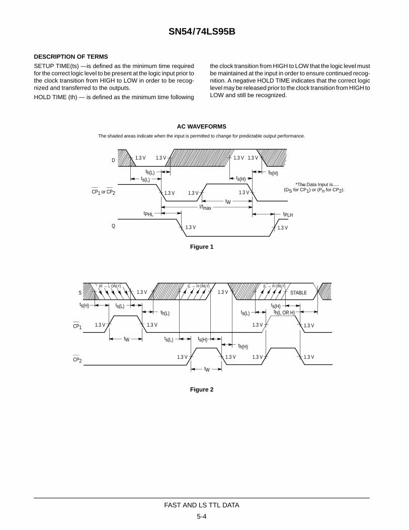
DESCRIPTION OF TERMS
SETUP TIME(ts) —is defined as the minimum time requiredfor the correct logic level to be present at the logic input prior tothe clock transition from HIGH to LOW in order to be recog-nized and transferred to the outputs.
HOLD TIME (th) — is defined as the minimum time following
the clock transition from HIGH to LOW that the logic level mustbe maintained at the input in order to ensure continued recog-nition. A negative HOLD TIME indicates that the correct logiclevel may be released prior to the clock transition from HIGH toLOW and still be recognized.
AC WAVEFORMS
Figure 1
Figure 2
The shaded areas indicate when the input is permitted to change for predictable output performance.
1.3 V 1.3 V 1.3 V 1.3 V
1.3 V
th(H)ts(H)ts(L)
th(L)
tWl/fmax
tPHL tPLH
*The Data Input is(DS for CP1) or (Pn for CP2).
D
CP1 or CP2
Q
1.3 V 1.3 V
1.3 V
1.3 V1.3 V
1.3 V
1.3 V1.3 V
1.3 V 1.3 V
ts(L)
ts(H)th(L)
ts(L)ts(H)
ts(L) ts(H)th(H)
tW
th(L OR H)
STABLE(H → L ONLY)
S
CP1
CP2
tW
1.3 V 1.3 V
1.3 V
1.3 V
(L → H ONLY) (L → H ONLY)
5-1
FAST AND LS TTL DATA
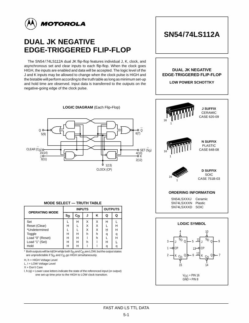
DUAL JK NEGATIVEEDGE-TRIGGERED FLIP-FLOP
The SN54/74LS112A dual JK flip-flop features individual J, K, clock, andasynchronous set and clear inputs to each flip-flop. When the clock goesHIGH, the inputs are enabled and data will be accepted. The logic level of theJ and K inputs may be allowed to change when the clock pulse is HIGH andthe bistable will perform according to the truth table as long as minimum set-upand hold time are observed. Input data is transferred to the outputs on thenegative-going edge of the clock pulse.
* Both outputs will be HIGH while both SD and CD are LOW, but the output statesare unpredictable if SD and CD go HIGH simultaneously.
H, h = HIGH Voltage LevelL, I = LOW Voltage LevelX = Don’t Carel, h (q) = Lower case letters indicate the state of the referenced input (or output)l, h (q) = one set-up time prior to the HIGH to LOW clock transition.
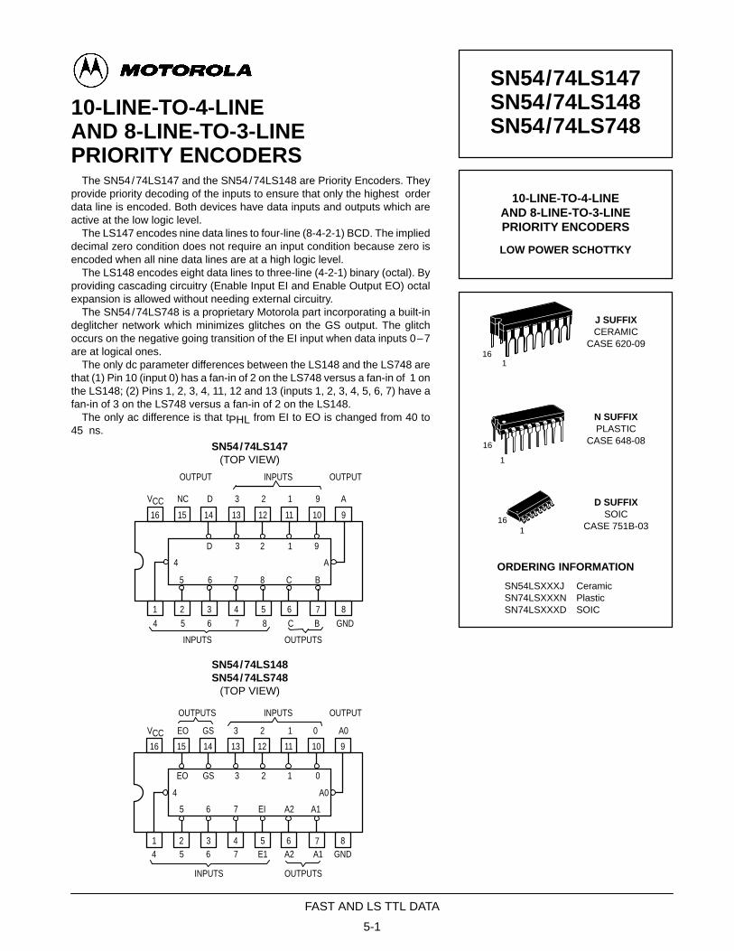
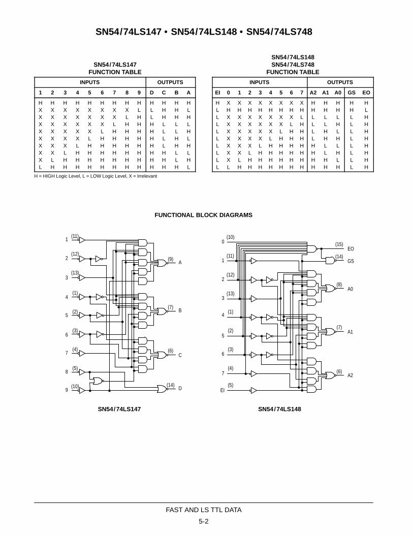
The SN54/74LS147 and the SN54/74LS148 are Priority Encoders. Theyprovide priority decoding of the inputs to ensure that only the highest orderdata line is encoded. Both devices have data inputs and outputs which areactive at the low logic level.
The LS147 encodes nine data lines to four-line (8-4-2-1) BCD. The implieddecimal zero condition does not require an input condition because zero isencoded when all nine data lines are at a high logic level.
The LS148 encodes eight data lines to three-line (4-2-1) binary (octal). Byproviding cascading circuitry (Enable Input EI and Enable Output EO) octalexpansion is allowed without needing external circuitry.
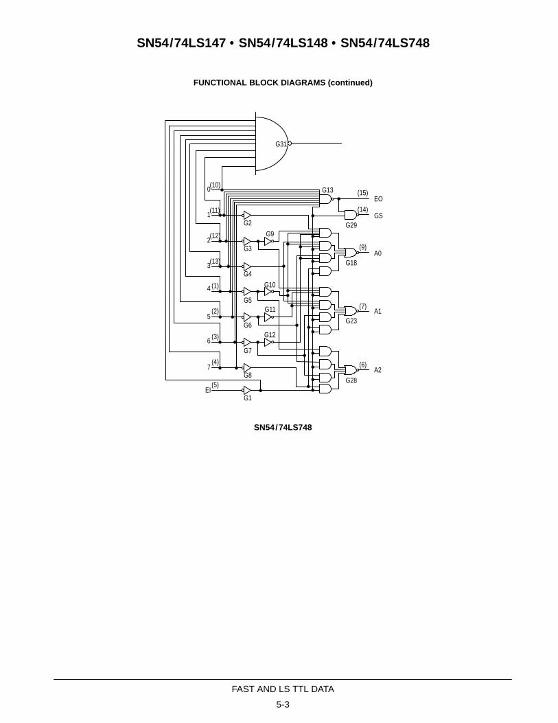
The SN54/74LS748 is a proprietary Motorola part incorporating a built-indeglitcher network which minimizes glitches on the GS output. The glitchoccurs on the negative going transition of the EI input when data inputs 0–7are at logical ones.
The only dc parameter differences between the LS148 and the LS748 arethat (1) Pin 10 (input 0) has a fan-in of 2 on the LS748 versus a fan-in of 1 onthe LS148; (2) Pins 1, 2, 3, 4, 11, 12 and 13 (inputs 1, 2, 3, 4, 5, 6, 7) have afan-in of 3 on the LS748 versus a fan-in of 2 on the LS148.
The only ac difference is that tPHL from EI to EO is changed from 40 to45 ns.
H H H H H H H H H H H H HX X X X X X X X L L H H LX X X X X X X L H L H H HX X X X X X L H H H L L LX X X X X L H H H H L L HX X X X L H H H H H L H LX X X L H H H H H H L H HX X L H H H H H H H H L LX L H H H H H H H H H L HL H H H H H H H H H H H L
SN54/74LS148SN54/74LS748
FUNCTION TABLE
INPUTS OUTPUTS
EI 0 1 2 3 4 5 6 7 A2 A1 A0 GS EO
H X X X X X X X X H H H H HL H H H H H H H H H H H H LL X X X X X X X L L L L L HL X X X X X X L H L L H L HL X X X X X L H H L H L L HL X X X X L H H H L H H L HL X X X L H H H H H L L L HL X X L H H H H H H L H L HL X L H H H H H H H H L L HL L H H H H H H H H H H L H
H = HIGH Logic Level, L = LOW Logic Level, X = Irrelevant
FUNCTIONAL BLOCK DIAGRAMS
SN54/74LS147 SN54/74LS148
1
2
3
4
5
6
7
8
9
(11)
(12)
(13)
(1)
(2)
(3)
(4)
(5)
(10)
(9)
(7)
(6)
(14)
A
B
C
D
0
1
2
3
4
5
6
7
EI
(10)
(11)
(12)
(13)
(1)
(2)
(3)
(4)
(5)
(15)EO
(14)GS
(8)A0
(7)A1
(6)A2
5-3
FAST AND LS TTL DATA
SN54/74LS147 • SN54/74LS148 • SN54/74LS748
FUNCTIONAL BLOCK DIAGRAMS (continued)
SN54/74LS748
G31
G2
G3
G4
G5
G6
G7
G8
G1
G9
G10
G11
G12
G130
1
2
3
4
5
6
7
EI
(10)
(11)
(12)
(13)
(1)
(2)
(3)
(4)
(5)
(15)EO
(14)GS
(9)A0
(7)A1
(6)A2
G29
G18
G23
G28
5-4
FAST AND LS TTL DATA
SN54/74LS147 • SN54/74LS148 • SN54/74LS748
GUARANTEED OPERATING RANGES
Symbol Parameter Min Typ Max Unit
VCC Supply Voltage 5474
4.54.75
5.05.0
5.55.25
V
TA Operating Ambient Temperature Range 5474
–550
2525
12570
°C
IOH Output Current — High 54, 74 –0.4 mA
IOL Output Current — Low 5474
4.08.0
mA
DC CHARACTERISTICS OVER OPERATING TEMPERATURE RANGE (unless otherwise specified)
S b l P
Limits
U i T C di iSymbol Parameter Min Typ Max Unit Test Conditions
VIH Input HIGH Voltage 2.0 VGuaranteed Input HIGH Voltage forAll Inputs
VIL Input LOW Voltage54 0.7
VGuaranteed Input LOW Voltage for
VIL Input LOW Voltage74 0.8
Vp g
All Inputs
VIK Input Clamp Diode Voltage –0.65 –1.5 V VCC = MIN, IIN = –18 mA
VOH Output HIGH Voltage54 2.5 3.5 V VCC = MIN, IOH = MAX, VIN = VIHVOH Output HIGH Voltage74 2.7 3.5 V
CC , OH , IN IHor VIL per Truth Table
VOL Output LOW Voltage54, 74 0.25 0.4 V IOL = 4.0 mA VCC = VCC MIN,
VIN = VIL or VIHVOL Output LOW Voltage74 0.35 0.5 V IOL = 8.0 mA
VIN = VIL or VIHper Truth Table
IIH
Input HIGH CurrentAll OthersInput 0 (LS748)Inputs 1–7 (LS148)Inputs 1–7 (LS748)
IOS Short Circuit Current (Note 1) –20 –100 mA VCC = MAX
ICCH Power Supply Current Output HIGH 17 mA VCC = MAX, All Inputs = 4.5 V
ICCL Output LOW 20 mAVCC = MAX, Inputs 7 & E1 = GNDAll Other Inputs = 4.5 V
Note 1: Not more than one output should be shorted at a time, nor for more than 1 second.
5-5
FAST AND LS TTL DATA
SN54/74LS147 • SN54/74LS148 • SN54/74LS748
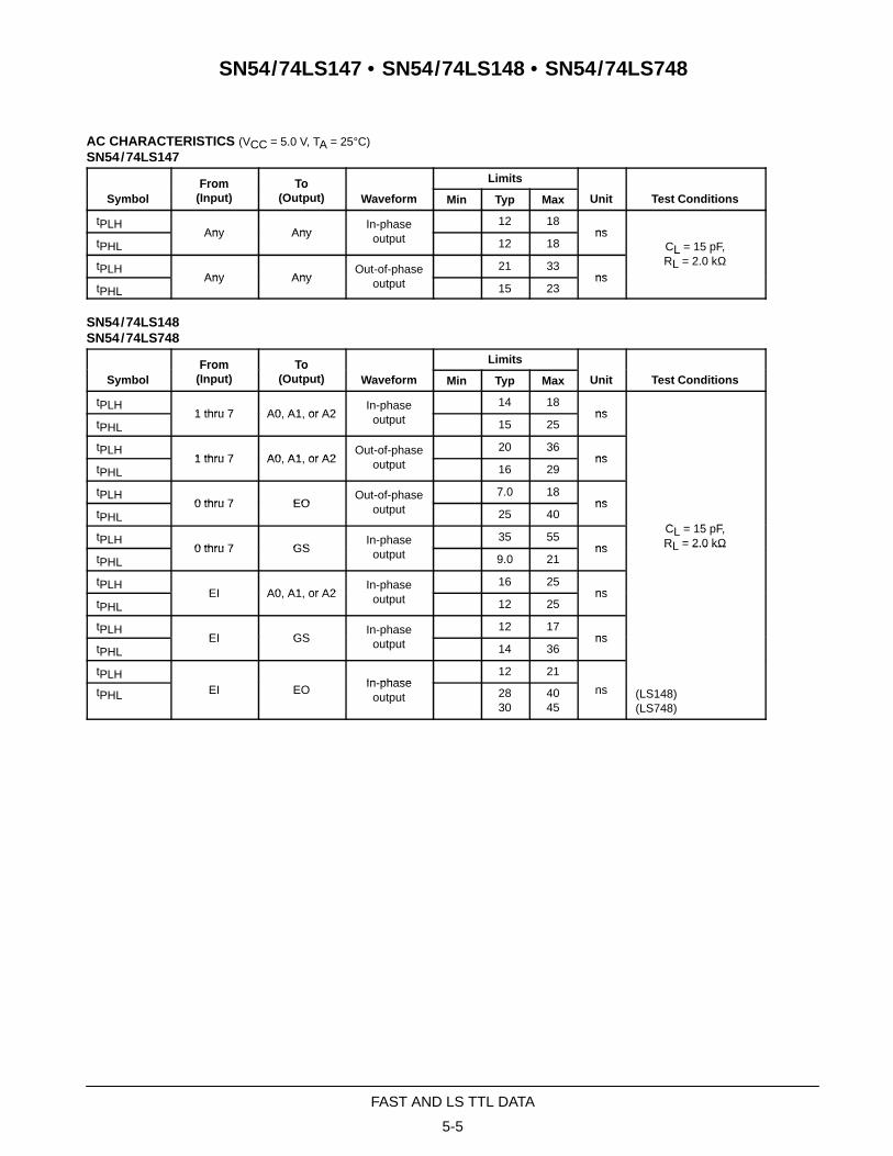
AC CHARACTERISTICS (VCC = 5.0 V, TA = 25°C)SN54/74LS147
S b lFrom To
W f
Limits
U i T C di iSymbolFrom
(Input)To
(Output) Waveform Min Typ Max Unit Test Conditions
tPLHAny Any
In-phase 12 18ns
C 15 FtPHLAny Any
poutput 12 18
nsCL = 15 pF,
tPLHAny Any
Out-of-phase 21 33ns
L p ,RL = 2.0 kΩ
tPHLAny Any
poutput 15 23
ns
SN54/74LS148SN54/74LS748
S b lFrom To
W f
Limits
U i T C di iSymbolFrom
(Input)To
(Output) Waveform Min Typ Max Unit Test Conditions
tPLH1 thru 7 A0 A1 or A2
In-phase 14 18ns
C 15 F
tPHL1 thru 7 A0, A1, or A2
poutput 15 25
ns
C 15 F
tPLH1 thru 7 A0 A1 or A2
Out-of-phase 20 36ns
C 15 F
tPHL1 thru 7 A0, A1, or A2
poutput 16 29
ns
C 15 F
tPLH0 thru 7 EO
Out-of-phase 7.0 18ns
C 15 FtPHL
0 thru 7 EOp
output 25 40ns
C 15 pFtPLH
0 thru 7 GSIn-phase 35 55
ns
CL = 15 pF,RL = 2.0 kΩ
tPHL0 thru 7 GS
poutput 9.0 21
ns RL = 2.0 kΩ
tPLHEI A0 A1 or A2
In-phase 16 25ns
tPHLEI A0, A1, or A2
poutput 12 25
ns
tPLHEI GS
In-phase 12 17ns
tPHLEI GS
poutput 14 36
ns
tPLHEI EO
In-phase12 21
tPHL EI EOIn-phaseoutput 28
304045
ns (LS148)(LS748)
5-1
FAST AND LS TTL DATA
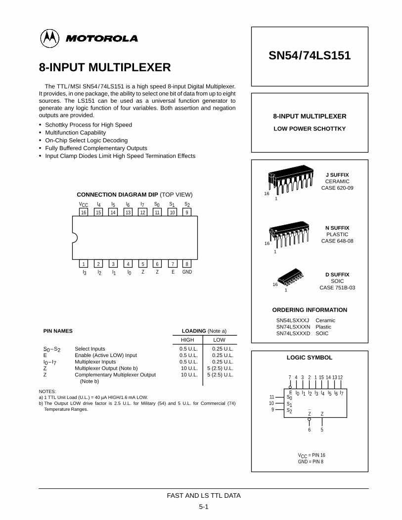
8-INPUT MULTIPLEXERThe TTL/MSI SN54/74LS151 is a high speed 8-input Digital Multiplexer.
It provides, in one package, the ability to select one bit of data from up to eightsources. The LS151 can be used as a universal function generator togenerate any logic function of four variables. Both assertion and negationoutputs are provided.
• Schottky Process for High Speed• Multifunction Capability• On-Chip Select Logic Decoding• Fully Buffered Complementary Outputs• Input Clamp Diodes Limit High Speed Termination Effects
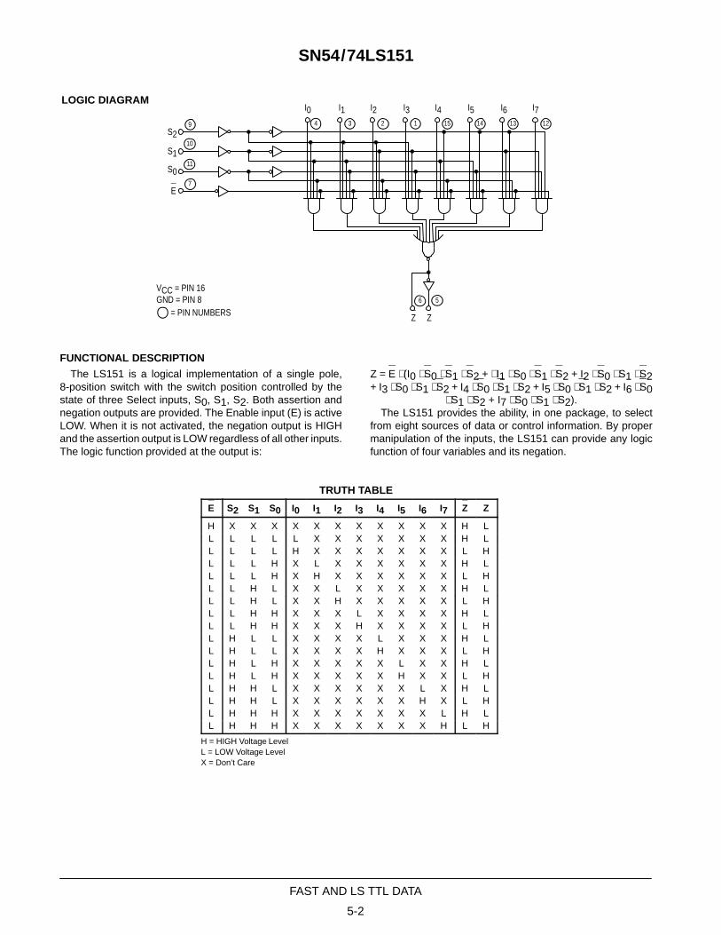
The LS151 is a logical implementation of a single pole,8-position switch with the switch position controlled by thestate of three Select inputs, S0, S1, S2. Both assertion andnegation outputs are provided. The Enable input (E) is activeLOW. When it is not activated, the negation output is HIGHand the assertion output is LOW regardless of all other inputs.The logic function provided at the output is:
⋅ S1 ⋅ S2 + I7 ⋅ S0 ⋅ S1 ⋅ S2).The LS151 provides the ability, in one package, to select
from eight sources of data or control information. By propermanipulation of the inputs, the LS151 can provide any logicfunction of four variables and its negation.
TRUTH TABLE
E S2 S1 S0 I0 I1 I2 I3 I4 I5 I6 I7 Z Z
H X X X X X X X X X X X H LL L L L L X X X X X X X H LL L L L H X X X X X X X L HL L L H X L X X X X X X H LL L L H X H X X X X X X L HL L H L X X L X X X X X H LL L H L X X H X X X X X L HL L H H X X X L X X X X H LL L H H X X X H X X X X L HL H L L X X X X L X X X H LL H L L X X X X H X X X L HL H L H X X X X X L X X H LL H L H X X X X X H X X L HL H H L X X X X X X L X H LL H H L X X X X X X H X L HL H H H X X X X X X X L H LL H H H X X X X X X X H L H
H = HIGH Voltage LevelL = LOW Voltage LevelX = Don’t Care
5-3
FAST AND LS TTL DATA
SN54/74LS151
GUARANTEED OPERATING RANGES
Symbol Parameter Min Typ Max Unit
VCC Supply Voltage 5474
4.54.75
5.05.0
5.55.25
V
TA Operating Ambient Temperature Range 5474
–550
2525
12570
°C
IOH Output Current — High 54, 74 –0.4 mA
IOL Output Current — Low 5474
4.08.0
mA
DC CHARACTERISTICS OVER OPERATING TEMPERATURE RANGE (unless otherwise specified)
S b l P
Limits
U i T C di iSymbol Parameter Min Typ Max Unit Test Conditions
VIH Input HIGH Voltage 2.0 VGuaranteed Input HIGH Voltage forAll Inputs
VIL Input LOW Voltage54 0.7
VGuaranteed Input LOW Voltage for
VIL Input LOW Voltage74 0.8
VGuaranteed Input LOW Voltage forAll Inputs
VIK Input Clamp Diode Voltage –0.65 –1.5 V VCC = MIN, IIN = –18 mA
VOH Output HIGH Voltage54 2.5 3.5 V VCC = MIN, IOH = MAX, VIN = VIHVOH Output HIGH Voltage74 2.7 3.5 V
VCC MIN, IOH MAX, VIN VIHor VIL per Truth Table
VOL Output LOW Voltage54, 74 0.25 0.4 V IOL = 4.0 mA VCC = VCC MIN,
VIN = VIL or VIHVOL Output LOW Voltage74 0.35 0.5 V IOL = 8.0 mA
VIN = VIL or VIHper Truth Table
IIH Input HIGH Current20 µA VCC = MAX, VIN = 2.7 V
IIH Input HIGH Current0.1 mA VCC = MAX, VIN = 7.0 V
IIL Input LOW Current –0.4 mA VCC = MAX, VIN = 0.4 V
IOS Short Circuit Current (Note 1) –20 –100 mA VCC = MAX
ICC Power Supply Current 10 mA VCC = MAX
Note 1: Not more than one output should be shorted at a time, nor for more than 1 second.
AC CHARACTERISTICS (TA = 25°C)
S b l P
Limits
U i T C di iSymbol Parameter Min Typ Max Unit Test Conditions
tPLHtPHL
Propagation DelaySelect to Output Z
2718
4330 ns
V 5 0 V
tPLHtPHL
Propagation DelaySelect to Output Z
1420
2332 ns
V 5 0 V
tPLHtPHL
Propagation DelayEnable to Output Z
2620
4232 ns
VCC = 5.0 V
tPLHtPHL
Propagation DelayEnable to Output Z
1518
2430 ns
VCC 5.0 VCL = 15 pF
tPLHtPHL
Propagation DelayData to Output Z
2016
3226 ns
tPLHtPHL
Propagation DelayData to Output Z
1312
2120 ns
AC WAVEFORMS
Figure 1 Figure 2
VIN
VOUT
1.3 V
tPHL
1.3 V
1.3 V
tPLH
1.3 V
VIN
VOUT
1.3 V
tPHL
1.3 V 1.3 V
1.3 V
tPLH
TL/F/6394
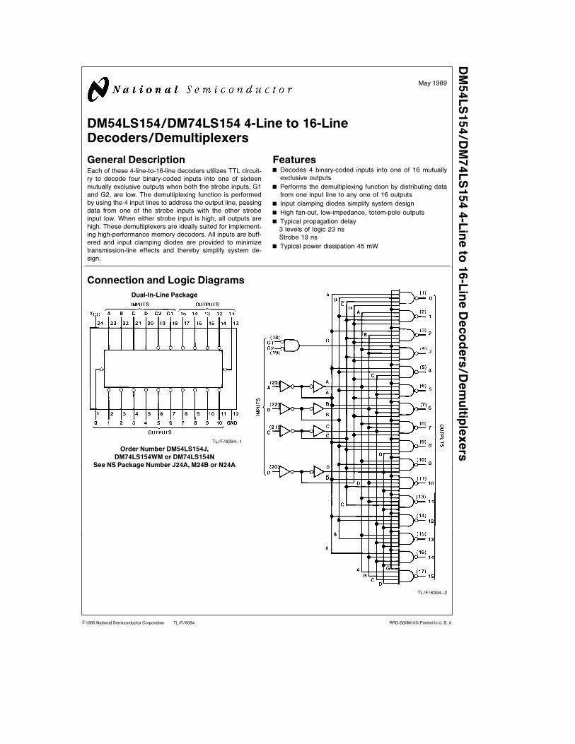
DM
54LS154/D
M74LS154
4-L
ine
to16-L
ine
Decoders
/D
em
ultip
lexers
May 1989
DM54LS154/DM74LS154 4-Line to 16-LineDecoders/Demultiplexers
General DescriptionEach of these 4-line-to-16-line decoders utilizes TTL circuit-
ry to decode four binary-coded inputs into one of sixteen
mutually exclusive outputs when both the strobe inputs, G1
and G2, are low. The demultiplexing function is performed
by using the 4 input lines to address the output line, passing
data from one of the strobe inputs with the other strobe
input low. When either strobe input is high, all outputs are
high. These demultiplexers are ideally suited for implement-
ing high-performance memory decoders. All inputs are buff-
ered and input clamping diodes are provided to minimize
transmission-line effects and thereby simplify system de-
sign.
FeaturesY Decodes 4 binary-coded inputs into one of 16 mutually
exclusive outputsY Performs the demultiplexing function by distributing data
from one input line to any one of 16 outputsY Input clamping diodes simplify system designY High fan-out, low-impedance, totem-pole outputsY Typical propagation delay
3 levels of logic 23 ns
Strobe 19 nsY Typical power dissipation 45 mW
Connection and Logic Diagrams
Dual-In-Line Package
TL/F/6394–1
Order Number DM54LS154J,
DM74LS154WM or DM74LS154N
See NS Package Number J24A, M24B or N24A
TL/F/6394–2
C1995 National Semiconductor Corporation RRD-B30M105/Printed in U. S. A.
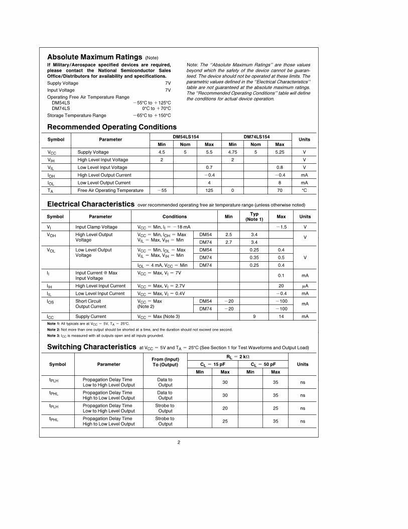
Absolute Maximum Ratings (Note)
If Military/Aerospace specified devices are required,
please contact the National Semiconductor Sales
Office/Distributors for availability and specifications.
Supply Voltage 7V
Input Voltage 7V
Operating Free Air Temperature Range
DM54LS b55§C to a125§CDM74LS 0§C to a70§C
Storage Temperature Range b65§C to a150§C
Note: The ‘‘Absolute Maximum Ratings’’ are those valuesbeyond which the safety of the device cannot be guaran-teed. The device should not be operated at these limits. Theparametric values defined in the ‘‘Electrical Characteristics’’table are not guaranteed at the absolute maximum ratings.The ‘‘Recommended Operating Conditions’’ table will definethe conditions for actual device operation.
Recommended Operating Conditions
Symbol ParameterDM54LS154 DM74LS154
UnitsMin Nom Max Min Nom Max
VCC Supply Voltage 4.5 5 5.5 4.75 5 5.25 V
VIH High Level Input Voltage 2 2 V
VIL Low Level Input Voltage 0.7 0.8 V
IOH High Level Output Current b0.4 b0.4 mA
IOL Low Level Output Current 4 8 mA
TA Free Air Operating Temperature b55 125 0 70 §C
Electrical Characteristics over recommended operating free air temperature range (unless otherwise noted)
Symbol Parameter Conditions MinTyp
Max Units(Note 1)
VI Input Clamp Voltage VCC e Min, II e b18 mA b1.5 V
VOH High Level Output VCC e Min, IOH e Max DM54 2.5 3.4V
Voltage VIL e Max, VIH e MinDM74 2.7 3.4
VOL Low Level Output VCC e Min, IOL e Max DM54 0.25 0.4Voltage VIL e Max, VIH e Min
DM74 0.35 0.5 V
IOL e 4 mA, VCC e Min DM74 0.25 0.4
II Input Current @ Max VCC e Max, VI e 7V0.1 mA
Input Voltage
IIH High Level Input Current VCC e Max, VI e 2.7V 20 mA
IIL Low Level Input Current VCC e Max, VI e 0.4V b0.4 mA
IOS Short Circuit VCC e Max DM54 b20 b100mA
Output Current (Note 2)DM74 b20 b100
ICC Supply Current VCC e Max (Note 3) 9 14 mA
Note 1: All typicals are at VCC e 5V, TA e 25§C.
Note 2: Not more than one output should be shorted at a time, and the duration should not exceed one second.
Note 3: ICC is measured with all outputs open and all inputs grounded.
Switching Characteristics at VCC e 5V and TA e 25§C (See Section 1 for Test Waveforms and Output Load)
From (Input)RL e 2 kX
Symbol Parameter To (Output) CL e 15 pF CL e 50 pF Units
Min Max Min Max
tPLH Propagation Delay Time Data to30 35 ns
Low to High Level Output Output
tPHL Propagation Delay Time Data to30 35 ns
High to Low Level Output Output
tPLH Propagation Delay Time Strobe to20 25 ns
Low to High Level Output Output
tPHL Propagation Delay Time Strobe to25 35 ns
High to Low Level Output Output
2
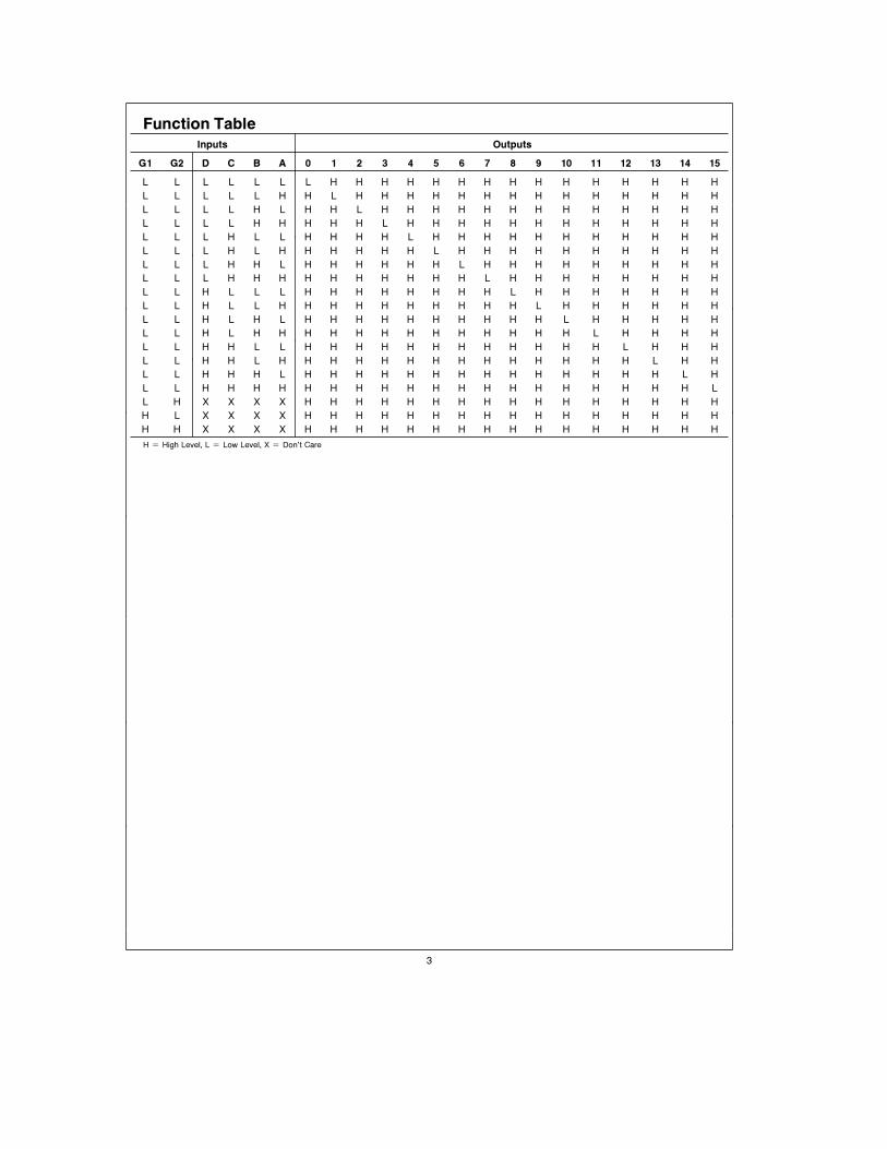
Function TableInputs Outputs
G1 G2 D C B A 0 1 2 3 4 5 6 7 8 9 10 11 12 13 14 15
L L L L L L L H H H H H H H H H H H H H H H
L L L L L H H L H H H H H H H H H H H H H H
L L L L H L H H L H H H H H H H H H H H H H
L L L L H H H H H L H H H H H H H H H H H H
L L L H L L H H H H L H H H H H H H H H H H
L L L H L H H H H H H L H H H H H H H H H H
L L L H H L H H H H H H L H H H H H H H H H
L L L H H H H H H H H H H L H H H H H H H H
L L H L L L H H H H H H H H L H H H H H H H
L L H L L H H H H H H H H H H L H H H H H H
L L H L H L H H H H H H H H H H L H H H H H
L L H L H H H H H H H H H H H H H L H H H H
L L H H L L H H H H H H H H H H H H L H H H
L L H H L H H H H H H H H H H H H H H L H H
L L H H H L H H H H H H H H H H H H H H L H
L L H H H H H H H H H H H H H H H H H H H L
L H X X X X H H H H H H H H H H H H H H H H
H L X X X X H H H H H H H H H H H H H H H H
H H X X X X H H H H H H H H H H H H H H H H
H e High Level, L e Low Level, X e Don’t Care
3
5-1
FAST AND LS TTL DATA
4-BIT ARITHMETICLOGIC UNIT
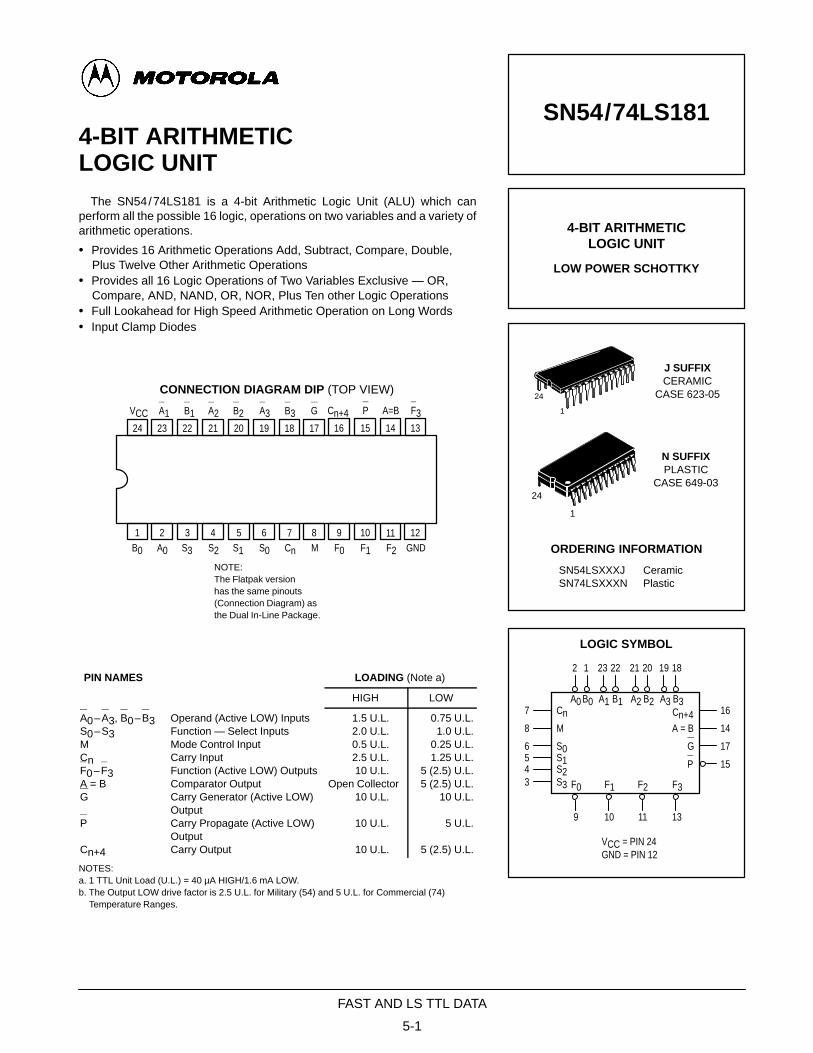
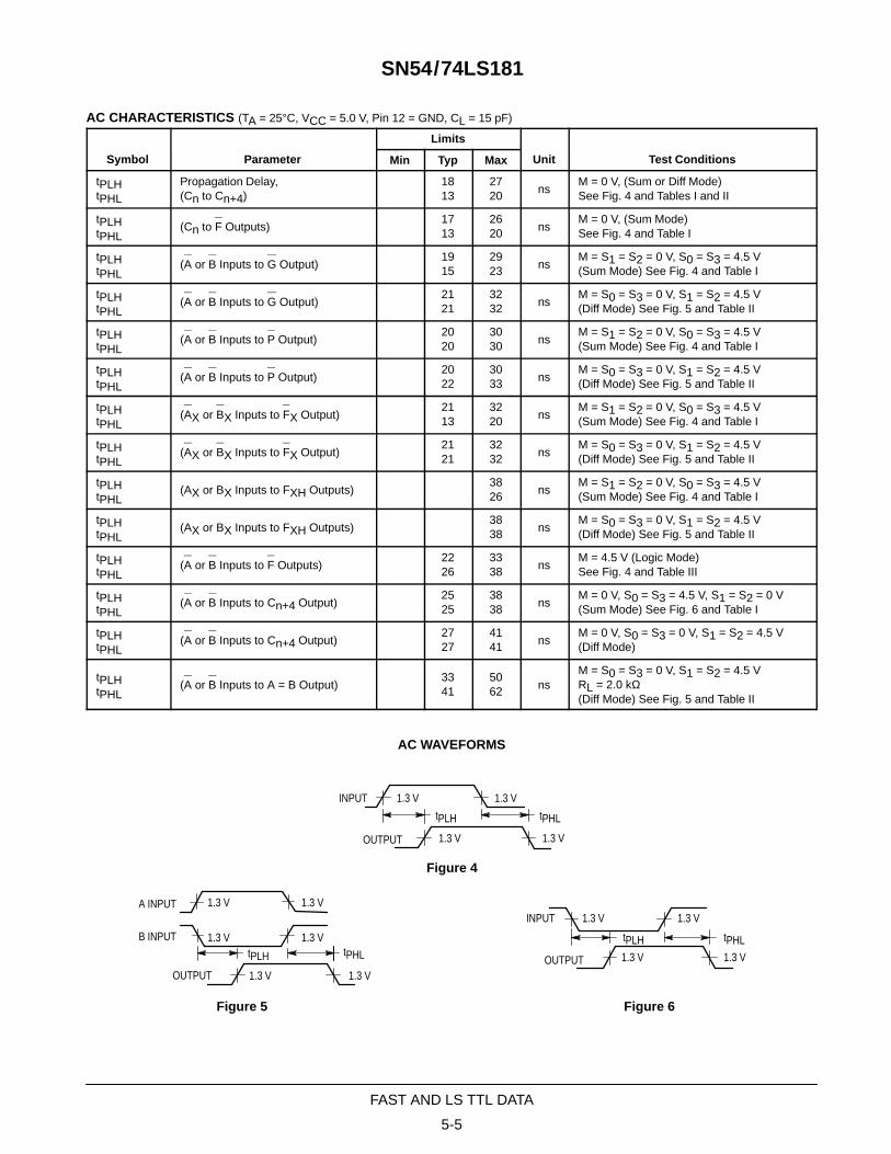
The SN54/74LS181 is a 4-bit Arithmetic Logic Unit (ALU) which canperform all the possible 16 logic, operations on two variables and a variety ofarithmetic operations.
NOTES:a. 1 TTL Unit Load (U.L.) = 40 µA HIGH/1.6 mA LOW.b. The Output LOW drive factor is 2.5 U.L. for Military (54) and 5 U.L. for Commercial (74)b. Temperature Ranges.
SN54/74LS181
4-BIT ARITHMETICLOGIC UNIT
LOW POWER SCHOTTKY
ORDERING INFORMATION
SN54LSXXXJ CeramicSN74LSXXXN Plastic
LOGIC SYMBOL
VCC = PIN 24GND = PIN 12
7
8
6543
9 10 11 13
15
17
14
16
2 1 23 22 21 20 19 18
CnM
S0S1S2S3
A0 B0 A1 B1 A2 B2 A3 B3
F0 F1 F2 F3
Cn+4A = B
G
P
24
1
J SUFFIXCERAMIC
CASE 623-05
24
1
N SUFFIXPLASTIC
CASE 649-03
5-2
FAST AND LS TTL DATA
SN54/74LS181
2
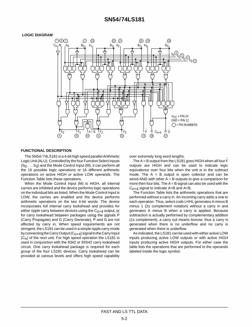
LOGIC DIAGRAM
S0 S1 S2 S3
Cn M
A = B Cn+4
A0 B0 A1 A2 A3B1 B2 B3
F0 F1 F2 F3 P G14
1
6
7
3
8
45
9 11 1610 13 15
VCC = PIN 24GND = PIN 12
= PIN NUMBERS
212223 20 1819
17
FUNCTIONAL DESCRIPTION
The SN54/74LS181 is a 4-bit high speed parallel ArithmeticLogic Unit (ALU). Controlled by the four Function Select Inputs(S0 . . . S3) and the Mode Control Input (M), it can perform allthe 16 possible logic operations or 16 different arithmeticoperations on active HIGH or active LOW operands. TheFunction Table lists these operations.
When the Mode Control Input (M) is HIGH, all internalcarries are inhibited and the device performs logic operationson the individual bits as listed. When the Mode Control Input isLOW, the carries are enabled and the device performsarithmetic operations on the two 4-bit words. The deviceincorporates full internal carry lookahead and provides foreither ripple carry between devices using the Cn+4 output, orfor carry lookahead between packages using the signals P(Carry Propagate) and G (Carry Generate), P and G are notaffected by carry in. When speed requirements are notstringent, the LS181 can be used in a simple ripple carry modeby connecting the Carry Output (Cn+4) signal to the Carry Input(Cn) of the next unit. For high speed operation the LS181 isused in conjunction with the 9342 or 93S42 carry lookaheadcircuit. One carry lookahead package is required for eachgroup of the four LS181 devices. Carry lookahead can beprovided at various levels and offers high speed capability
over extremely long word lengths.The A = B output from the LS181 goes HIGH when all four F
outputs are HIGH and can be used to indicate logicequivalence over four bits when the unit is in the subtractmode. The A = B output is open collector and can bewired-AND with other A = B outputs to give a comparison formore then four bits. The A = B signal can also be used with theCn+4 signal to indicate A>B and A<B.
The Function Table lists the arithmetic operations that areperformed without a carry in. An incoming carry adds a one toeach operation. Thus, select code LHHL generates A minus Bminus 1 (2s complement notation) without a carry in andgenerates A minus B when a carry is applied. Becausesubtraction is actually performed by complementary addition(1s complement), a carry out means borrow; thus a carry isgenerated when there is no underflow and no carry isgenerated when there is underflow.
As indicated, the LS181 can be used with either active LOWinputs producing active LOW outputs or with active HIGHinputs producing active HIGH outputs. For either case thetable lists the operations that are performed to the operandslabeled inside the logic symbol.
5-3
FAST AND LS TTL DATA
SN54/74LS181
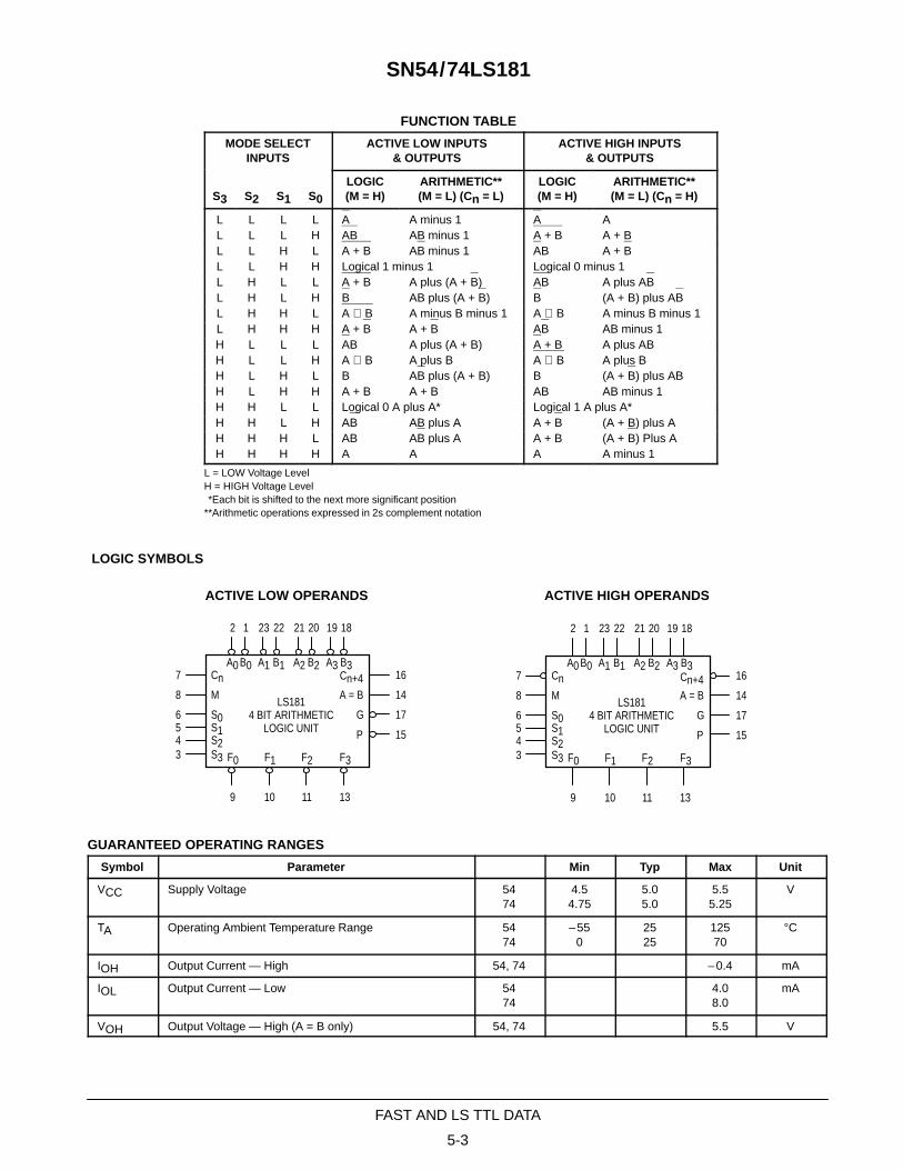
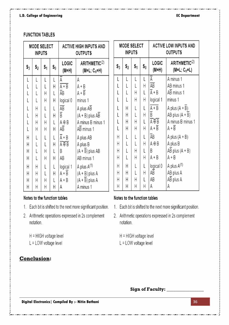
FUNCTION TABLE
MODE SELECTINPUTS
ACTIVE LOW INPUTS& OUTPUTS
ACTIVE HIGH INPUTS& OUTPUTS
S3 S2 S1 S0LOGIC(M = H)
ARITHMETIC**(M = L) (Cn = L)
LOGIC(M = H)
ARITHMETIC**(M = L) (Cn = H)
L L L L A A minus 1 A AL L L H AB AB minus 1 A + B A + BL L H L A + B AB minus 1 AB A + BL L H H Logical 1 minus 1 Logical 0 minus 1L H L L A + B A plus (A + B) AB A plus ABL H L H B AB plus (A + B) B (A + B) plus ABL H H L A ⊕ B A minus B minus 1 A ⊕ B A minus B minus 1L H H H A + B A + B AB AB minus 1H L L L AB A plus (A + B) A + B A plus ABH L L H A ⊕ B A plus B A ⊕ B A plus BH L H L B AB plus (A + B) B (A + B) plus ABH L H H A + B A + B AB AB minus 1H H L L Logical 0 A plus A* Logical 1 A plus A*H H L H AB AB plus A A + B (A + B) plus AH H H L AB AB plus A A + B (A + B) Plus AH H H H A A A A minus 1
L = LOW Voltage LevelH = HIGH Voltage Level**Each bit is shifted to the next more significant position**Arithmetic operations expressed in 2s complement notation
LOGIC SYMBOLS
ACTIVE LOW OPERANDS ACTIVE HIGH OPERANDS
7
8
6543
9 10 11 13
15
17
14
16
2 1 23 22 21 20 19 18
CnM
S0S1S2S3
A0 B0 A1 B1 A2 B2 A3 B3
F0 F1 F2 F3
Cn+4A = B
G
P
LS1814 BIT ARITHMETIC
LOGIC UNIT
7
8
6543
9 10 11 13
15
17
14
16
2 1 23 22 21 20 19 18
CnM
S0S1S2S3
A0 B0 A1 B1 A2 B2 A3 B3
F0 F1 F2 F3
Cn+4A = B
G
P
LS1814 BIT ARITHMETIC
LOGIC UNIT
GUARANTEED OPERATING RANGES
Symbol Parameter Min Typ Max Unit
VCC Supply Voltage 5474
4.54.75
5.05.0
5.55.25
V
TA Operating Ambient Temperature Range 5474
–550
2525
12570
°C
IOH Output Current — High 54, 74 –0.4 mA
IOL Output Current — Low 5474
4.08.0
mA
VOH Output Voltage — High (A = B only) 54, 74 5.5 V
5-4
FAST AND LS TTL DATA
SN54/74LS181
DC CHARACTERISTICS OVER OPERATING TEMPERATURE RANGE (unless otherwise specified)
S b l P
Limits
U i T C di iSymbol Parameter Min Typ Max Unit Test Conditions
VIH Input HIGH Voltage 2.0 VGuaranteed Input HIGH Voltage forAll Inputs
VIL Input LOW Voltage54 0.7
VGuaranteed Input LOW Voltage for
VIL Input LOW Voltage74 0.8
Vp g
All Inputs
VIK Input Clamp Diode Voltage –0.65 –1.5 V VCC = MIN, IIN = –18 mA
VOH Output HIGH Voltage54 2.5 3.5 V VCC = MIN, IOH = MAX, VIN = VIHVOH Output HIGH Voltage74 2.7 3.5 V
CC , OH , IN IHor VIL per Truth Table
V
Output LOW Voltage 54, 74 0.25 0.4 V IOL = 4.0 mA
V V MINV
p gExcept G and P 74 0.35 0.5 V IOL = 8.0 mA VCC = VCC MIN,
VOL Output G 54, 74 0.7 V IOL = 16 mA
VCC VCC MIN,VIN = VIL or VIHper Truth Table
Output P5474
0.60.5 V IOL = 8.0 mA
per Truth Table
IOH Output HIGH Current 54, 74 100 µAVCC = MIN, IOH = MAX, VIN = VIHor VIL per Truth Table
IIH
Input HIGH CurrentMode InputAny A or B InputAny S InputCn Input
206080100
µA VCC = MAX, VIN = 2.7 V
IIHMode InputAny A or B InputAny S InputCn Input
0.10.30.40.5
mA VCC = MAX, VIN = 7.0 V
IIL
Input LOW CurrentMode InputAny A or B InputAny S InputCn Input
–0.4–1.2–1.6–2.0
mA VCC = MAX, VIN = 0.4 V
IOS Short Circuit Current (Note 2) –20 –100 mA VCC = MAX
I
Power Supply Current 54 32
A V MAXICC
pp ySee Note 1A 74 34
mA VCC = MAXICC
See Note 1B54 35
mA VCC = MAX
See Note 1B74 37
Note 1.With outputs open, ICC is measured for the following conditions:A. S0 through S3, M, and A inputs are at 4.5 V, all other inputs are grounded.B. S0 through S3 and M are at 4.5 V, all other inputs are grounded.
Note 2: Not more than one output should be shorted at a time, nor for more than 1 second.
M = S0 = S3 = 0 V, S1 = S2 = 4.5 VRL = 2.0 kΩ(Diff Mode) See Fig. 5 and Table II
AC WAVEFORMS
Figure 5 Figure 6
Figure 4
1.3 V 1.3 V
1.3 V1.3 V
1.3 V 1.3 V
1.3 V1.3 V
1.3 V1.3 V
1.3 V1.3 V
1.3 V 1.3 V
INPUT
INPUTA INPUT
B INPUT
tPLH
tPLHtPLH
tPHL
tPHLtPHL
OUTPUT
OUTPUTOUTPUT
5-6
FAST AND LS TTL DATA
SN54/74LS181
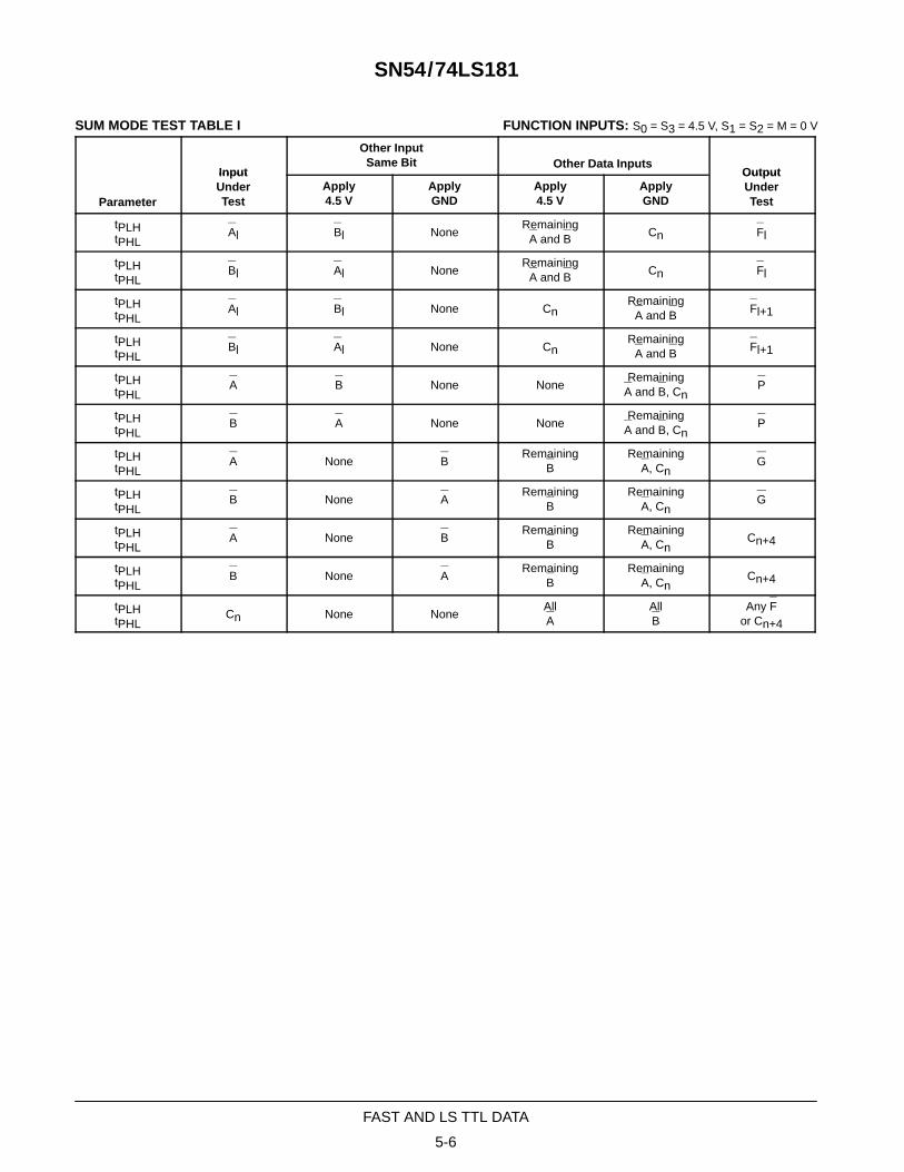
SUM MODE TEST TABLE I FUNCTION INPUTS: S0 = S3 = 4.5 V, S1 = S2 = M = 0 V
P
Input
Other InputSame Bit Other Data Inputs
Output
Parameter
InputUnderTest
Apply4.5 V
ApplyGND
Apply4.5 V
ApplyGND
OutputUnderTest
tPLHtPHL
Al Bl NoneRemaining
A and B Cn Fl
tPLHtPHL
Bl Al NoneRemaining
A and B Cn Fl
tPLHtPHL
Al Bl None CnRemaining
A and B Fl+1
tPLHtPHL
Bl Al None CnRemaining
A and B Fl+1
tPLHtPHL
A B None NoneRemaining
A and B, CnP
tPLHtPHL
B A None NoneRemaining
A and B, CnP
tPLHtPHL
A None BRemaining
BRemaining
A, CnG
tPLHtPHL
B None ARemaining
BRemaining
A, CnG
tPLHtPHL
A None BRemaining
BRemaining
A, CnCn+4
tPLHtPHL
B None ARemaining
BRemaining
A, CnCn+4
tPLHtPHL
Cn None NoneAllA
AllB
Any For Cn+4
5-7
FAST AND LS TTL DATA
SN54/74LS181
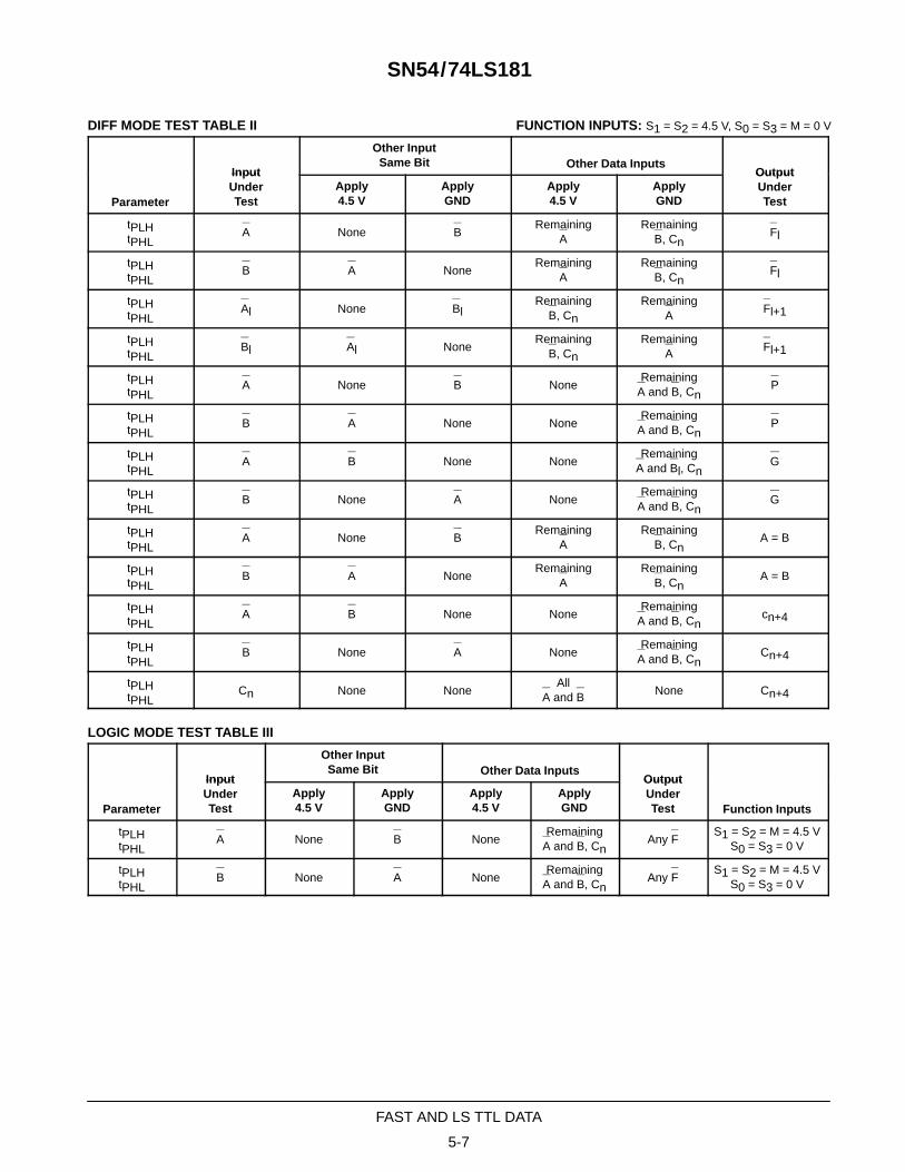
DIFF MODE TEST TABLE II FUNCTION INPUTS: S1 = S2 = 4.5 V, S0 = S3 = M = 0 V
P
Input
Other InputSame Bit Other Data Inputs
Output
Parameter
InputUnderTest
Apply4.5 V
ApplyGND
Apply4.5 V
ApplyGND
OutputUnderTest
tPLHtPHL
A None BRemaining
ARemaining
B, CnFl
tPLHtPHL
B A NoneRemaining
ARemaining
B, CnFl
tPLHtPHL
Al None BlRemaining
B, Cn
RemainingA Fl+1
tPLHtPHL
Bl Al NoneRemaining
B, Cn
RemainingA Fl+1
tPLHtPHL
A None B NoneRemaining
A and B, CnP
tPLHtPHL
B A None NoneRemaining
A and B, CnP
tPLHtPHL
A B None NoneRemaining
A and Bl, CnG
tPLHtPHL
B None A NoneRemaining
A and B, CnG
tPLHtPHL
A None BRemaining
ARemaining
B, CnA = B
tPLHtPHL
B A NoneRemaining
ARemaining
B, CnA = B
tPLHtPHL
A B None NoneRemaining
A and B, Cncn+4
tPLHtPHL
B None A NoneRemaining
A and B, CnCn+4
tPLHtPHL
Cn None NoneAll
A and B None Cn+4
LOGIC MODE TEST TABLE III
P
Input
Other InputSame Bit Other Data Inputs
Output
F i IParameter
InputUnderTest
Apply4.5 V
ApplyGND
Apply4.5 V
ApplyGND
OutputUnderTest Function Inputs
tPLHtPHL
A None B NoneRemaining
A and B, CnAny F
S1 = S2 = M = 4.5 VS0 = S3 = 0 V
tPLHtPHL
B None A NoneRemaining
A and B, CnAny F
S1 = S2 = M = 4.5 VS0 = S3 = 0 V
5-1
FAST AND LS TTL DATA
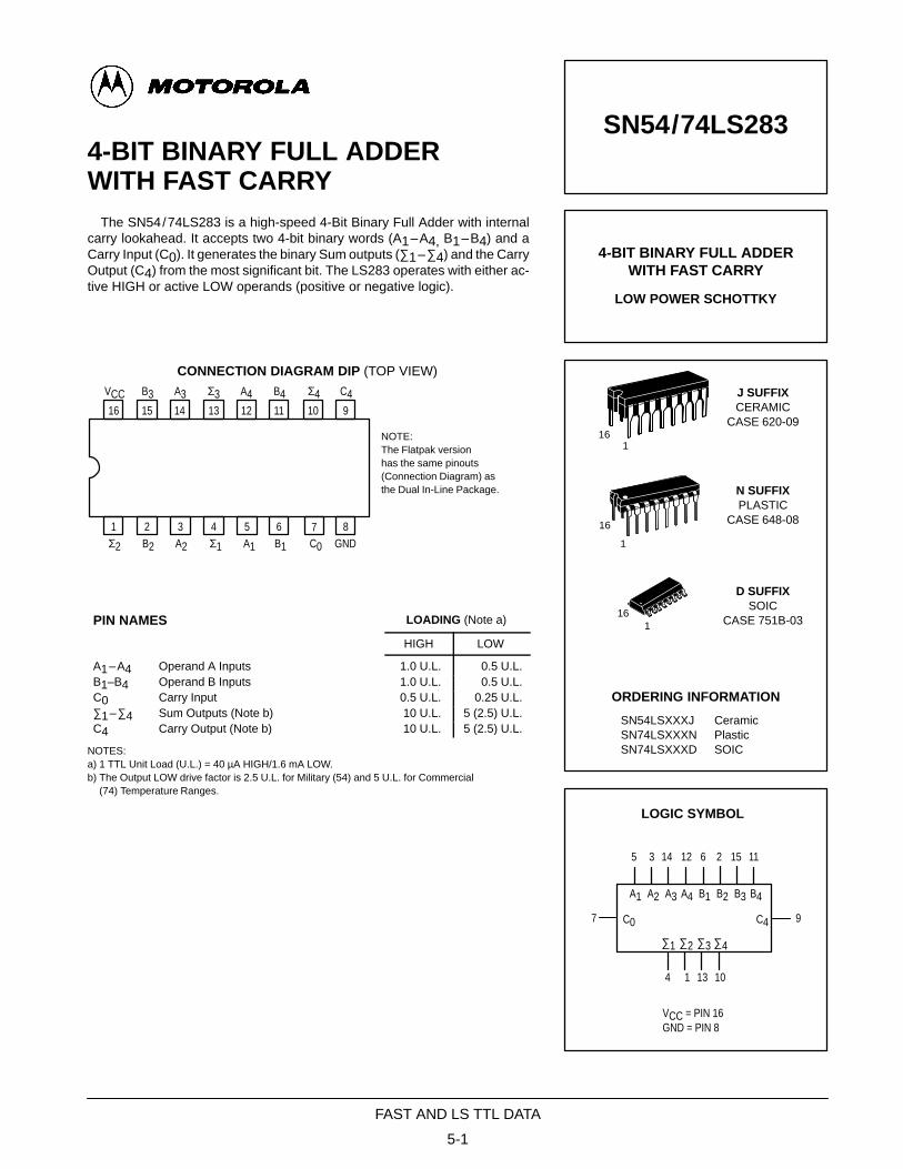
4-BIT BINARY FULL ADDERWITH FAST CARRY
The SN54/74LS283 is a high-speed 4-Bit Binary Full Adder with internalcarry lookahead. It accepts two 4-bit binary words (A1–A4, B1–B4) and aCarry Input (C0). It generates the binary Sum outputs (∑1–∑4) and the CarryOutput (C4) from the most significant bit. The LS283 operates with either ac-tive HIGH or active LOW operands (positive or negative logic).
14 13 12 11 10 9
1 2 3 4 5 6 7
16 15
8
VCC
Σ2
B3 A3 Σ3 A4 Σ4B4 C4
B2 A2 Σ1 A1 B1 C0 GND
CONNECTION DIAGRAM DIP (TOP VIEW)
NOTE:The Flatpak versionhas the same pinouts(Connection Diagram) asthe Dual In-Line Package.
PIN NAMES LOADING (Note a)
HIGH LOW
A1–A4 Operand A Inputs 1.0 U.L. 0.5 U.L.B1–B4 Operand B Inputs 1.0 U.L. 0.5 U.L.C0 Carry Input 0.5 U.L. 0.25 U.L.∑1–∑4 Sum Outputs (Note b) 10 U.L. 5 (2.5) U.L.C4 Carry Output (Note b) 10 U.L. 5 (2.5) U.L.
NOTES:a) 1 TTL Unit Load (U.L.) = 40 µA HIGH/1.6 mA LOW.b) The Output LOW drive factor is 2.5 U.L. for Military (54) and 5 U.L. for Commercial
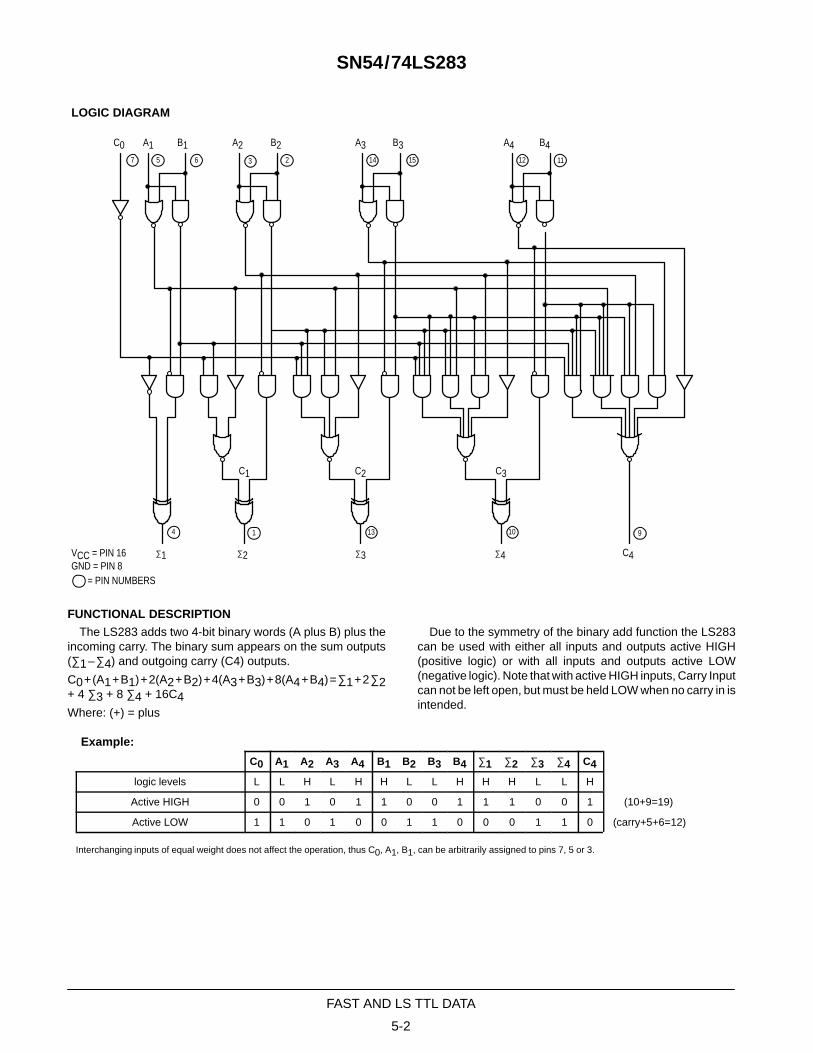
The LS283 adds two 4-bit binary words (A plus B) plus theincoming carry. The binary sum appears on the sum outputs(∑1–∑4) and outgoing carry (C4) outputs.
Due to the symmetry of the binary add function the LS283can be used with either all inputs and outputs active HIGH(positive logic) or with all inputs and outputs active LOW(negative logic). Note that with active HIGH inputs, Carry Inputcan not be left open, but must be held LOW when no carry in isintended.