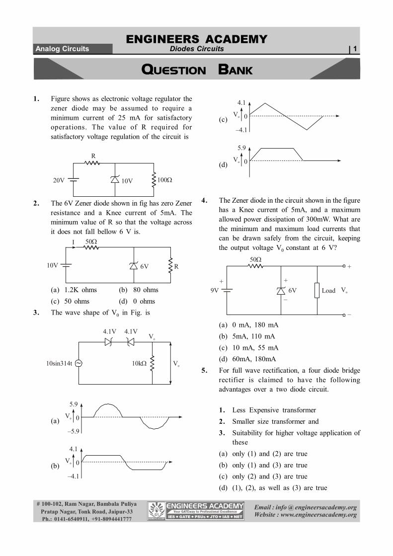
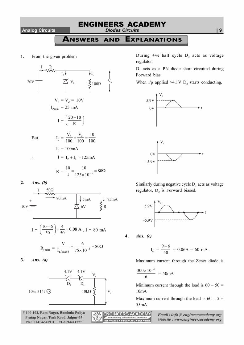
Email : info @ engineersacademy.org Website : www.engineersacademy.org # 100-102, Ram Nagar, Bambala Puliya Pratap Nagar, Tonk Road, Jaipur-33 Ph.: 0141-6540911, +91-8094441777 ENGINEERS ACADEMY Analog Circuits Diodes Circuits | 1 1. Figure shows as electronic voltage regulator the zener diode may be assumed to require a minimum current of 25 mA for satisfactory operations. The value of R required for satisfactory voltage regulation of the circuit is R 20V 10V 1002. The 6V Zener diode shown in fig has zero Zener resistance and a Knee current of 5mA. The minimum value of R so that the voltage across it does not fall bellow 6 V is. I 506V R 10V (a) 1.2K ohms (b) 80 ohms (c) 50 ohms (d) 0 ohms 3. The wave shape of V 0 in Fig. is ~ 10kV o V o 4.1V 4.1V 10sin314t (a) V o 0 5.9 –5.9 (b) V o 0 4.1 –4.1 (c) V o 0 4.1 –4.1 (d) V o 0 5.9 4. The Zener diode in the circuit shown in the figure has a Knee current of 5mA, and a maximum allowed power dissipation of 300mW. What are the minimum and maximum load currents that can be drawn safely from the circuit, keeping the output voltage V 0 constant at 6 V? + + – – V o Load 6V + 9V 50(a) 0 mA, 180 mA (b) 5mA, 110 mA (c) 10 mA, 55 mA (d) 60mA, 180mA 5. For full wave rectification, a four diode bridge rectifier is claimed to have the following advantages over a two diode circuit. 1. Less Expensive transformer 2. Smaller size transformer and 3. Suitability for higher voltage application of these (a) only (1) and (2) are true (b) only (1) and (3) are true (c) only (2) and (3) are true (d) (1), (2), as well as (3) are true QUESTION BANK
Transcript
Email : info @ engineersacademy.orgWebsite : www.engineersacademy.org
1. Figure shows as electronic voltage regulator thezener diode may be assumed to require aminimum current of 25 mA for satisfactoryoperations. The value of R required forsatisfactory voltage regulation of the circuit is
R
20V 10V 100
2. The 6V Zener diode shown in fig has zero Zenerresistance and a Knee current of 5mA. Theminimum value of R so that the voltage acrossit does not fall bellow 6 V is.
I 50
6V R10V
(a) 1.2K ohms (b) 80 ohms(c) 50 ohms (d) 0 ohms
3. The wave shape of V0 in Fig. is
~ 10k Vo
Vo
4.1V 4.1V
10sin314t
(a)Vo 0
5.9
–5.9
(b)Vo 0
4.1
–4.1
(c)Vo 0
4.1
–4.1
(d)Vo 0
5.9
4. The Zener diode in the circuit shown in the figurehas a Knee current of 5mA, and a maximumallowed power dissipation of 300mW. What arethe minimum and maximum load currents thatcan be drawn safely from the circuit, keepingthe output voltage V0 constant at 6 V?
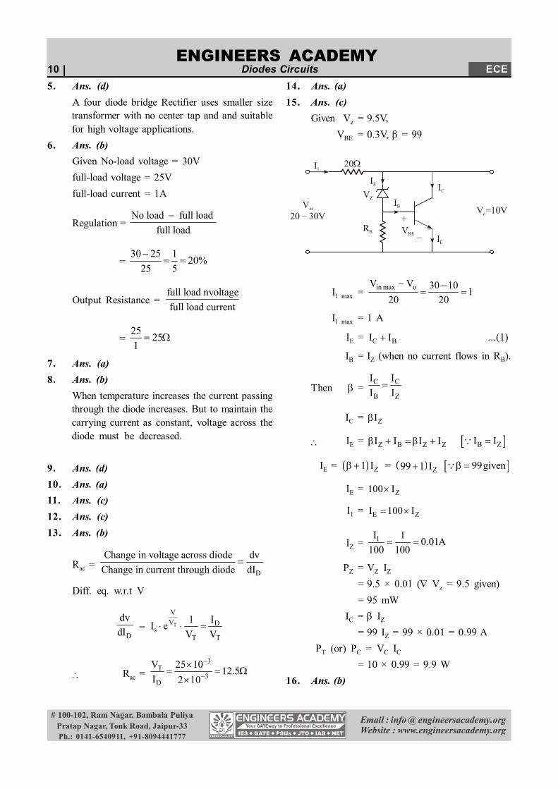
6. A dc power supply has a No-load voltage of30V and a full-load voltage of 25V at a full-loadcurrent of 1A. The output resistance and loadregulation, respectively are(a) 5 and 20% (b) 25 and 20%(c) 5 and 16.7% (d) 25 and 16.7%
7. The mobility of an electron in a conductorexpressed in terms of(a) Cm2/V–sec (b) Cm/V–sec(c) Cm2/V (d) Cm2/sec
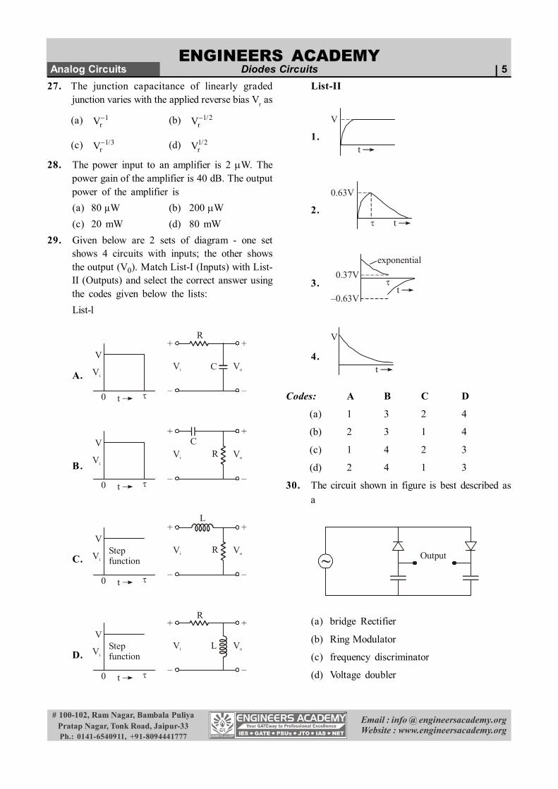
8. As temperature is increased, the voltage acrossa diode carrying a constant current.(a) Increases(b) Decreases(c) Remains Constant(d) May increase or decrease depending upon
the doping levels in the junction9. In a single-stage differential amplifier, the output
offset voltage is basically dependent on themismatch of(a) VBE, IB and (b) VBE and IB
(c) IB and (d) VBE and 10. The input resistance of a common emitter stage
can be increased by1. un-bypass emitter resistance2. bootstrapping3. biasing it at low quiescent current4. using compounded BJTsThe correct sequence in descending order of theeffectiveness of these methods is(a) 2, 4, 1,3 (b) 4, 3, 2, 1(c) 2, 4, 3, 1 (d) 4, 2, 3, 1
11. The diode ‘D’ is ideal in the network shown inthe given figure. The current ‘I’ will be
D
I
4V
2 k
(a) –mA (b) zero(c) 2mA (d) 4mA
12. The transfer characteristic of the network shownin the given figure is represented as
V0Vi
+–
R
VR
D
(a)
V0
Slope = 1
Vi
(b)
V0
Slope = 1
Vi
(c)
V0
Slope = 1
Vi
VR
VR
(d)
V0
Slope = 1
VR
Vi
Email : info @ engineersacademy.orgWebsite : www.engineersacademy.org
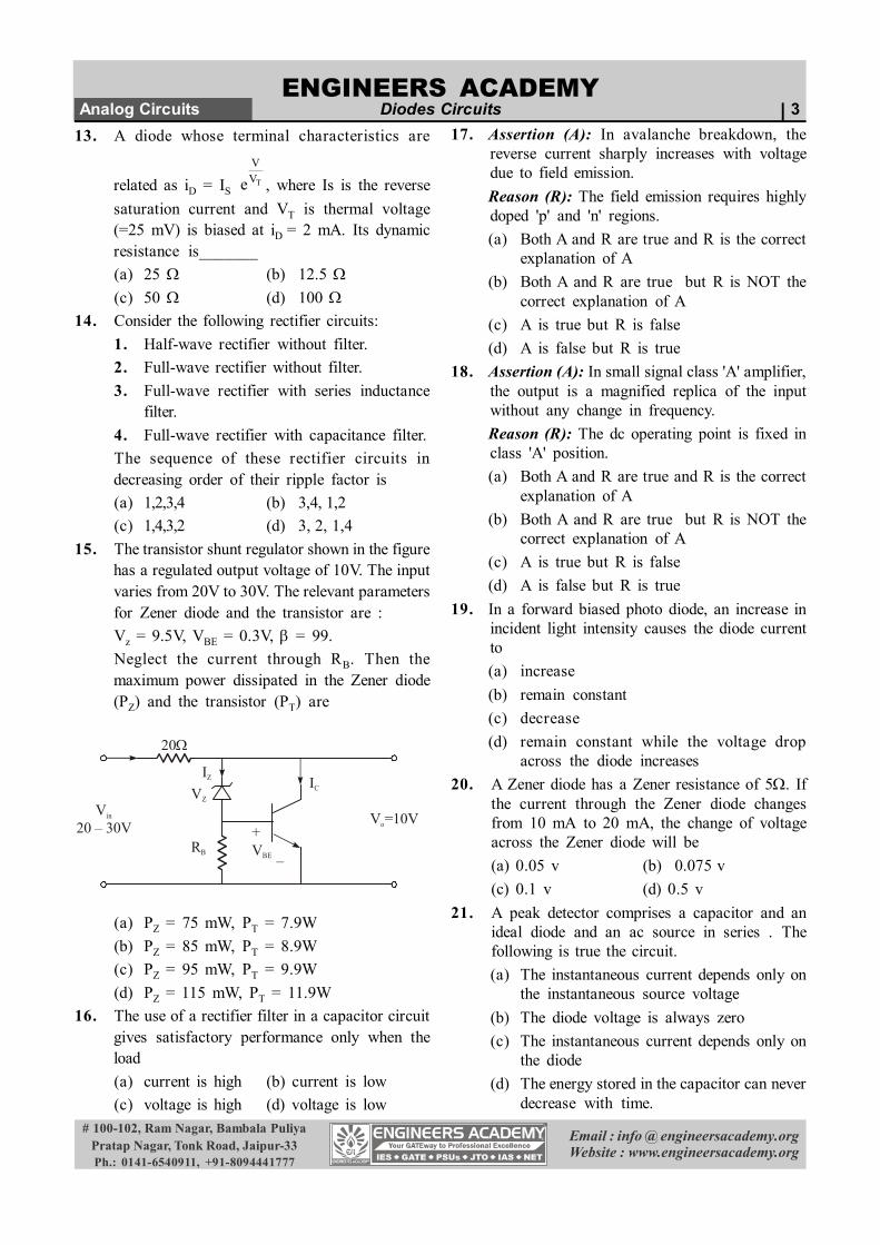
saturation current and VT is thermal voltage(=25 mV) is biased at iD = 2 mA. Its dynamicresistance is_______(a) 25 (b) 12.5 (c) 50 (d) 100
14. Consider the following rectifier circuits:1. Half-wave rectifier without filter.2. Full-wave rectifier without filter.3. Full-wave rectifier with series inductance
filter.4. Full-wave rectifier with capacitance filter.The sequence of these rectifier circuits indecreasing order of their ripple factor is(a) 1,2,3,4 (b) 3,4, 1,2(c) 1,4,3,2 (d) 3, 2, 1,4
15. The transistor shunt regulator shown in the figurehas a regulated output voltage of 10V. The inputvaries from 20V to 30V. The relevant parametersfor Zener diode and the transistor are :Vz = 9.5V, VBE = 0.3V, = 99.Neglect the current through RB. Then themaximum power dissipated in the Zener diode(PZ) and the transistor (PT) are
16. The use of a rectifier filter in a capacitor circuitgives satisfactory performance only when theload(a) current is high (b) current is low(c) voltage is high (d) voltage is low
17. Assertion (A): In avalanche breakdown, thereverse current sharply increases with voltagedue to field emission.Reason (R): The field emission requires highlydoped 'p' and 'n' regions.(a) Both A and R are true and R is the correct
explanation of A(b) Both A and R are true but R is NOT the
correct explanation of A(c) A is true but R is false(d) A is false but R is true
18. Assertion (A): In small signal class 'A' amplifier,the output is a magnified replica of the inputwithout any change in frequency.Reason (R): The dc operating point is fixed inclass 'A' position.(a) Both A and R are true and R is the correct
explanation of A(b) Both A and R are true but R is NOT the
correct explanation of A(c) A is true but R is false(d) A is false but R is true
19. In a forward biased photo diode, an increase inincident light intensity causes the diode currentto(a) increase(b) remain constant(c) decrease(d) remain constant while the voltage drop
across the diode increases20. A Zener diode has a Zener resistance of 5. If
the current through the Zener diode changesfrom 10 mA to 20 mA, the change of voltageacross the Zener diode will be(a) 0.05 v (b) 0.075 v(c) 0.1 v (d) 0.5 v
21. A peak detector comprises a capacitor and anideal diode and an ac source in series . Thefollowing is true the circuit.(a) The instantaneous current depends only on
the instantaneous source voltage(b) The diode voltage is always zero(c) The instantaneous current depends only on
the diode(d) The energy stored in the capacitor can never
decrease with time.
Email : info @ engineersacademy.orgWebsite : www.engineersacademy.org
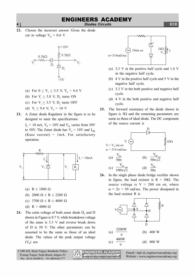
22. Choose the incorrect answer Given the diodecut in voltage VD = 0.6 V
D1D2
V0
+10V
+5V
9.5k0.5kVi
(a) For 0 < V1 < 3.5 V, V0 = 4.4 V(b) For Vi > 3.8 V, D2 turns ON(c) For Vi > 3.5 V, D2 turns OFF(d) Vi > 9.4 V, V0 = 10 V
23. A Zener diode Regulator in the figure is to bedesigned to meet the specifications:IL = 10 mA, V0 = 10V and Vin varies from 30Vto 50V. The Zener diode has Vz = 10V and IZK
(Knee current) = 1mA. For satisfactoryoperation.
RL
R
IZ
VZVin Vo
I = 10mAL
(a) R 1800 (b) 2000 R 2200 (c) 3700 R 4000 (d) R > 4000
24. The cutin voltage of both zener diode Dz and Dshown in Figure is 0.7 V, while breakdown voltageof the zener is 3.3 V and reverse break downof D is 50 V. The other parameters can beassumed to be the same as those of an idealdiode. The values of the peak output voltage(V0) are
~=314rad/sec
10sin t 1kV
0I
(a) 3.3 V in the positive half cycle and 1.4 Vin the negative half cycle.
(b) 4 V in the positive half cycle and 5 V in thenegative half cycle.
(c) 3.3 V in the both positive and negative halfcycle.
(d) 4 V in the both positive and negative halfcycle.
25. The forward resistance of the diode shown infigure is 5 and the remaining parameters aresame as those of ideal diode. The DC componentof the source current is
~Vi
D
45V = V sin t
= 314 rad/seci m
(a) mV50
(b) mV50 2
(c) mV100 2
(d) mV50
26. In the single phase diode bridge rectifier shownin figure, the load resistor is R = 50. Thesource voltage is V = 200 sin t, where = 2 × 50 rad/sec. The power dissipated inthe load resistor R is
~V
D
BAR
(a)3200W
(b) 400 W
(c)400W
(d) 800 W
Email : info @ engineersacademy.orgWebsite : www.engineersacademy.org
27. The junction capacitance of linearly gradedjunction varies with the applied reverse bias Vr as
(a) 1rV (b) 1/2
rV
(c) 1/3rV (d) 1/2
rV
28. The power input to an amplifier is 2 W. Thepower gain of the amplifier is 40 dB. The outputpower of the amplifier is(a) 80 µW (b) 200 W(c) 20 mW (d) 80 mW
29. Given below are 2 sets of diagram - one setshows 4 circuits with inputs; the other showsthe output (V0). Match List-I (Inputs) with List-II (Outputs) and select the correct answer usingthe codes given below the lists:List-l
A.
t
V
Vi
0
+
–
Vi
+
–
Vo
R
C
B.
t
V
Vi
0
+
–
Vi
+
–
VoRC
C.
t
V
Vi
0
+
–
Vi
+
–
VoRStep function
L
D.
t
V
Vi
0
+
–
Vi
+
–
Vo
R
Step function
L
List-II
1.t
V
2.t
0.63V
3.t
0.37V
–0.63V
exponential
4.
V
t
Codes: A B C D
(a) 1 3 2 4
(b) 2 3 1 4
(c) 1 4 2 3
(d) 2 4 1 3
30. The circuit shown in figure is best described asa
~ Output
(a) bridge Rectifier
(b) Ring Modulator
(c) frequency discriminator
(d) Voltage doubler
Email : info @ engineersacademy.orgWebsite : www.engineersacademy.org
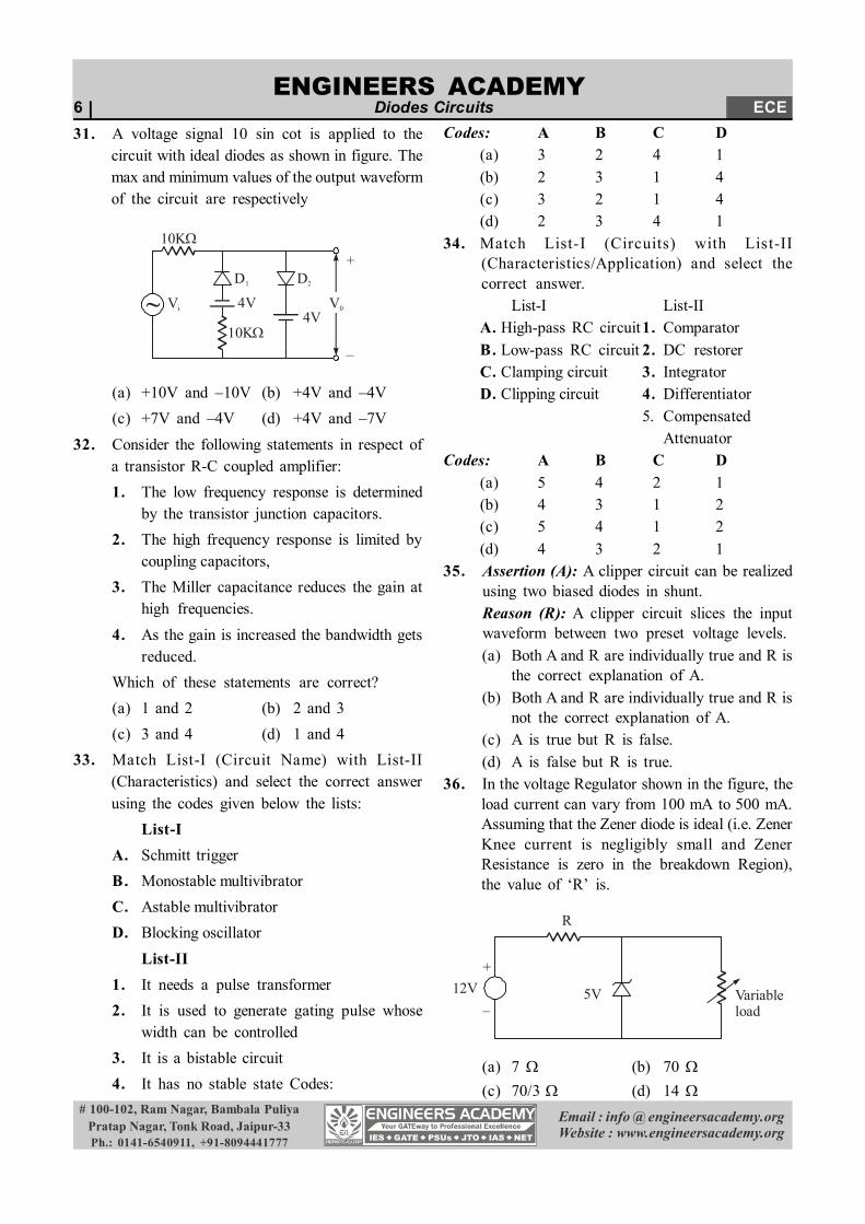
31. A voltage signal 10 sin cot is applied to thecircuit with ideal diodes as shown in figure. Themax and minimum values of the output waveformof the circuit are respectively
~
10K
Vi
D1
4V
10K4V
D2
V0
+
–
(a) +10V and –10V (b) +4V and –4V(c) +7V and –4V (d) +4V and –7V
32. Consider the following statements in respect ofa transistor R-C coupled amplifier:1. The low frequency response is determined
by the transistor junction capacitors.2. The high frequency response is limited by
coupling capacitors,3. The Miller capacitance reduces the gain at
high frequencies.4. As the gain is increased the bandwidth gets
reduced.Which of these statements are correct?(a) 1 and 2 (b) 2 and 3(c) 3 and 4 (d) 1 and 4
33. Match List-I (Circuit Name) with List-II(Characteristics) and select the correct answerusing the codes given below the lists:
Codes: A B C D(a) 5 4 2 1(b) 4 3 1 2(c) 5 4 1 2(d) 4 3 2 1
35. Assertion (A): A clipper circuit can be realizedusing two biased diodes in shunt.Reason (R): A clipper circuit slices the inputwaveform between two preset voltage levels.(a) Both A and R are individually true and R is
the correct explanation of A.(b) Both A and R are individually true and R is
not the correct explanation of A.(c) A is true but R is false.(d) A is false but R is true.
36. In the voltage Regulator shown in the figure, theload current can vary from 100 mA to 500 mA.Assuming that the Zener diode is ideal (i.e. ZenerKnee current is negligibly small and ZenerResistance is zero in the breakdown Region),the value of ‘R’ is.
+
–12V
R
5V Variable load
(a) 7 (b) 70 (c) 70/3 (d) 14
Email : info @ engineersacademy.orgWebsite : www.engineersacademy.org
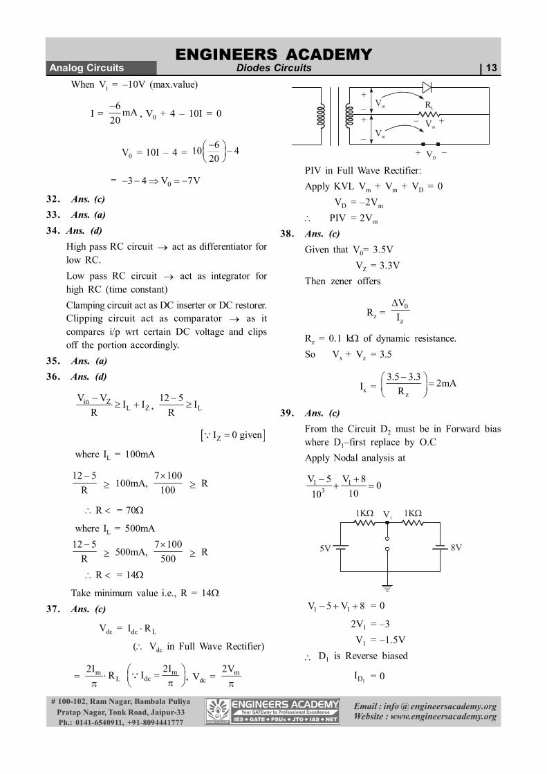
37. In a full - Wave Rectifier using two ideal diodes,Vdc and Vm are the dc and peak values of thevoltage respectively across a Resistive load. IfPIV is the peak inverse voltage of the diodes,then the appropriate relationships for this Rectifierare
(a) mdc m
VV , PIV 2V
(b) mdc m
2VV , PIV V
(c) mdc m
2VV , PIV 2V
(d) mdc m
VV , PIV V
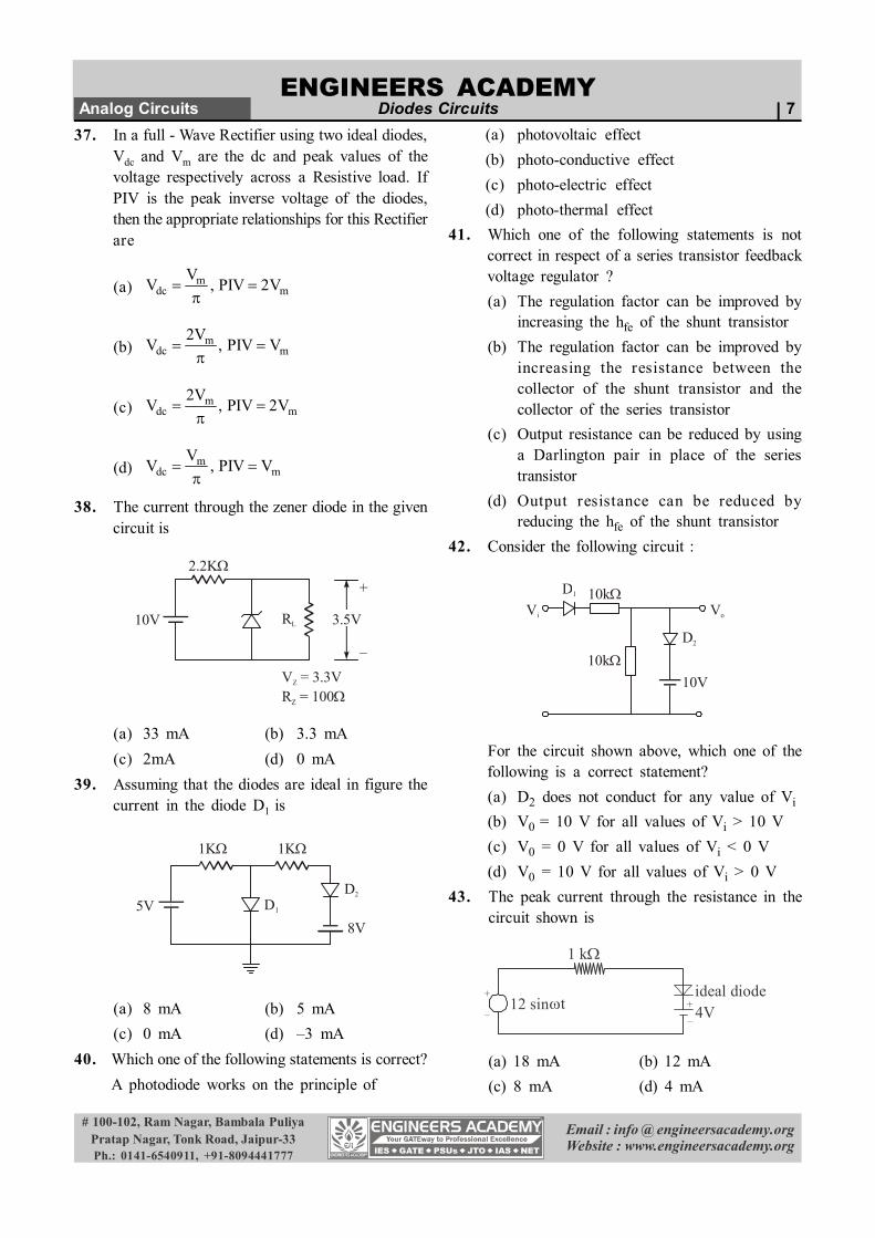
38. The current through the zener diode in the givencircuit is
10V RL
2.2K+
–
3.5V
V = 3.3VR = 100
Z
Z
(a) 33 mA (b) 3.3 mA(c) 2mA (d) 0 mA
39. Assuming that the diodes are ideal in figure thecurrent in the diode D1 is
1K 1K
5V D1
D2
8V
(a) 8 mA (b) 5 mA(c) 0 mA (d) –3 mA
40. Which one of the following statements is correct?A photodiode works on the principle of
41. Which one of the following statements is notcorrect in respect of a series transistor feedbackvoltage regulator ?(a) The regulation factor can be improved by
increasing the hfe of the shunt transistor(b) The regulation factor can be improved by
increasing the resistance between thecollector of the shunt transistor and thecollector of the series transistor
(c) Output resistance can be reduced by usinga Darlington pair in place of the seriestransistor
(d) Output resistance can be reduced byreducing the hfe of the shunt transistor
42. Consider the following circuit :
10kD2
10V
D1 10kVi Vo
For the circuit shown above, which one of thefollowing is a correct statement?(a) D2 does not conduct for any value of Vi
(b) V0 = 10 V for all values of Vi > 10 V(c) V0 = 0 V for all values of Vi < 0 V(d) V0 = 10 V for all values of Vi > 0 V
43. The peak current through the resistance in thecircuit shown is
12 sint
1 k
ideal diode4V+
–
+
–
(a) 18 mA (b) 12 mA(c) 8 mA (d) 4 mA
Email : info @ engineersacademy.orgWebsite : www.engineersacademy.org
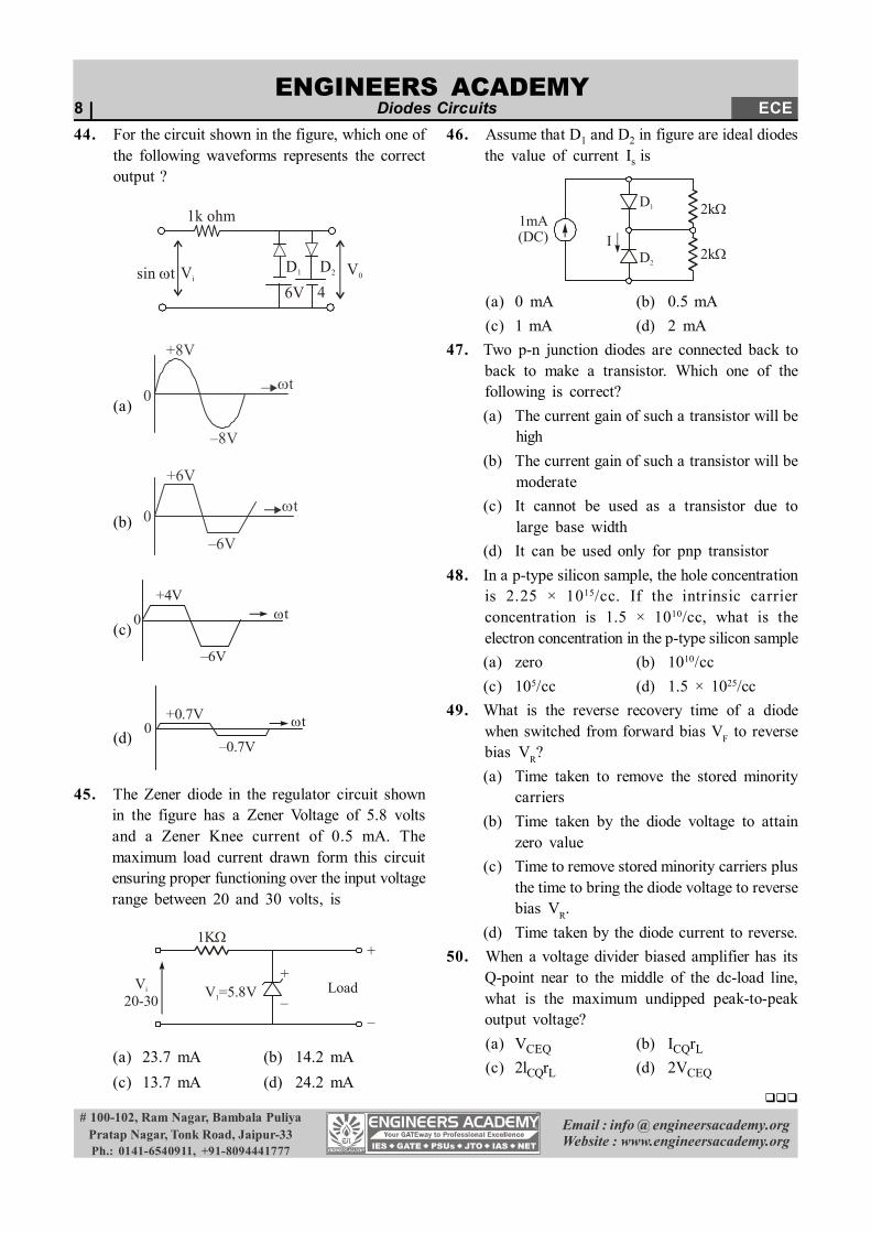
44. For the circuit shown in the figure, which one ofthe following waveforms represents the correctoutput ?
1k ohm
Visin t D1 D2 V0
6V 4
(a)
+8V
0
–8V
t
(b)–6V
+6V
t0
(c)
+4Vt
–6V
0
(d) 0+0.7V
–0.7V
t
45. The Zener diode in the regulator circuit shownin the figure has a Zener Voltage of 5.8 voltsand a Zener Knee current of 0.5 mA. Themaximum load current drawn form this circuitensuring proper functioning over the input voltagerange between 20 and 30 volts, is
1K
V20-30
i V =5.8V1
+
–Load
+
–
(a) 23.7 mA (b) 14.2 mA(c) 13.7 mA (d) 24.2 mA
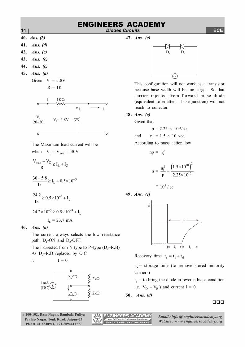
46. Assume that D1 and D2 in figure are ideal diodesthe value of current Is is
1mA(DC)
D1
D2
I
2k
2k
(a) 0 mA (b) 0.5 mA(c) 1 mA (d) 2 mA
47. Two p-n junction diodes are connected back toback to make a transistor. Which one of thefollowing is correct?(a) The current gain of such a transistor will be
high(b) The current gain of such a transistor will be
moderate(c) It cannot be used as a transistor due to
large base width(d) It can be used only for pnp transistor
48. In a p-type silicon sample, the hole concentrationis 2.25 × 10¹⁵/cc. If the intrinsic carrierconcentration is 1.5 × 10¹⁰/cc, what is theelectron concentration in the p-type silicon sample(a) zero (b) 1010/cc(c) 105/cc (d) 1.5 × 1025/cc
49. What is the reverse recovery time of a diodewhen switched from forward bias VF to reversebias VR?(a) Time taken to remove the stored minority
carriers(b) Time taken by the diode voltage to attain
zero value(c) Time to remove stored minority carriers plus
the time to bring the diode voltage to reversebias VR.
(d) Time taken by the diode current to reverse.50. When a voltage divider biased amplifier has its
Q-point near to the middle of the dc-load line,what is the maximum undipped peak-to-peakoutput voltage?(a) VCEQ (b) ICQrL(c) 2lCQrL (d) 2VCEQ
Email : info @ engineersacademy.orgWebsite : www.engineersacademy.org
During +ve half cycle D2 acts as voltageregulator.D1 acts as a PN diode short circuited duringForward bias.When i/p applied >4.1V D2 starts conducting.
V0
t
5.9V
0V
V0
t
–5.9V
0V
Similarly during negative cycle D1 acts as voltageregulator, D2 is Forward biased.
V0
5.9V
–5.9V
t
4. Ans. (c)
Iin =9 650
= 0.06A = 60 mA
Maximum current through the Zener diode is
3300 106
= 50mA
Minimum current through the load is 60 – 50 =10mAMaximum current through the load is 60 – 5 =55mA
ANSWERS AND EXPLANATIONS
Email : info @ engineersacademy.orgWebsite : www.engineersacademy.org
5. Ans. (d)A four diode bridge Rectifier uses smaller sizetransformer with no center tap and and suitablefor high voltage applications.
6. Ans. (b)Given No-load voltage = 30Vfull-load voltage = 25Vfull-load current = 1A
Regulation =No load full load
full load
=30 25 1 20%
25 5
Output Resistance = full load nvoltagefull load current
=25 251
7. Ans. (a)8. Ans. (b)
When temperature increases the current passingthrough the diode increases. But to maintain thecarrying current as constant, voltage across thediode must be decreased.
9. Ans. (d)10. Ans. (a)11. Ans. (c)12. Ans. (c)13. Ans. (b)
Rac = D
Change in voltage across diode dvChange in current through diode dI
Diff. eq. w.r.t V
D
dvdI = T
VV D
sT T
I1I eV V
Rac =3
T3
D
V 25 10 12.5I 2 10
14. Ans. (a)15. Ans. (c)
Given Vz = 9.5V,VBE = 0.3V, = 99
IZ
VZ
RB
+
–VBE
IC
V =10VoV
20 – 30Vin
20
IB
IE
I1
I1 max = in max oV V 30 10 120 20
I1 max = 1 A
IE = C BI I ...(1)
IB = IZ (when no current flows in RB).
Then =C C
B Z
I II I
IC = ZI
IE = Z B Z ZI I I I B ZI I
IE = Z1 I = Z99 1 I 99given
IE = Z100 I
I1 = E ZI 100 I
IZ = 1I 1 0.01A100 100
PZ = VZ IZ
= 9.5 × 0.01 ( Vz = 9.5 given)= 95 mW
IC = IZ
= 99 IZ = 99 × 0.01 = 0.99 A PT (or) PC = VC IC
= 10 × 0.99 = 9.9 W16. Ans. (b)
Email : info @ engineersacademy.orgWebsite : www.engineersacademy.org
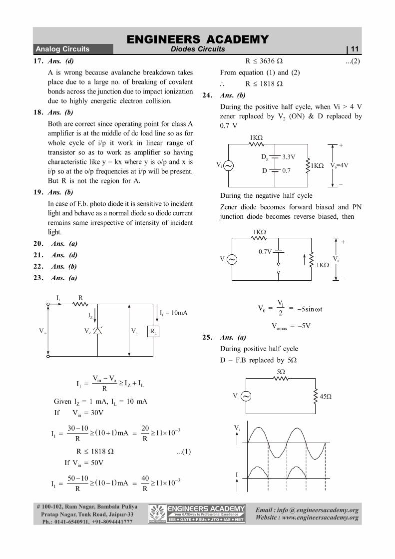
17. Ans. (d)A is wrong because avalanche breakdown takesplace due to a large no. of breaking of covalentbonds across the junction due to impact ionizationdue to highly energetic electron collision.
18. Ans. (b)Both are correct since operating point for class Aamplifier is at the middle of dc load line so as forwhole cycle of i/p it work in linear range oftransistor so as to work as amplifier so havingcharacteristic like y = kx where y is o/p and x isi/p so at the o/p frequencies at i/p will be present.But R is not the region for A.
19. Ans. (b)In case of F.b. photo diode it is sensitive to incidentlight and behave as a normal diode so diode currentremains same irrespective of intensity of incidentlight.
20. Ans. (a)21. Ans. (d)22. Ans. (b)23. Ans. (a)
RL
R
IZ
VZVin Vo
I = 10mAL
I1
I1 = in oZ L
V V I IR
Given IZ = 1 mA, IL = 10 mA If Vin = 30V
I1 = 30 10 10 1 mAR
= 320 11 10R
R 1818 ...(1)If Vin = 50V
I1 = 50 10 10 1 mAR
= 340 11 10R
R 3636 ...(2)From equation (1) and (2) R 1818
24. Ans. (b)During the positive half cycle, when Vi > 4 Vzener replaced by V2 (ON) & D replaced by0.7 V
~Vi
1K
3.3V
0.71K
+
–
Dz
DV =4V0
During the negative half cycleZener diode becomes forward biased and PNjunction diode becomes reverse biased, then
~Vi
1K
1K–
+
V0
0.7V
V0 = iV2
= 5sin t
Vomax = –5V25. Ans. (a)
During positive half cycleD – F.B replaced by 5
~
5
45Vi
I
Vi
Email : info @ engineersacademy.orgWebsite : www.engineersacademy.org
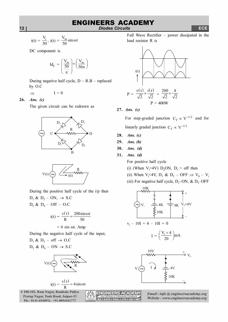
High pass RC circuit act as differentiator forlow RC.Low pass RC circuit act as integrator forhigh RC (time constant)Clamping circuit act as DC inserter or DC restorer.Clipping circuit act as comparator as itcompares i/p wrt certain DC voltage and clipsoff the portion accordingly.
35. Ans. (a)36. Ans. (d)
in ZL Z
V V I IR
, L12 5 I
R
ZI 0 given
where IL = 100mA
12 5R
100mA, 7 100
100
R
R = 70
where IL = 500mA12 5
R
500mA, 7 100
500
R
R = 14
Take minimum value i.e., R = 1437. Ans. (c)
Vdc = dc LI R
( Vdc in Full Wave Rectifier)
= mL
2I R
mdc
2II
, Vdc = m2V
+–
–
+
Vm RL
Vm
+–
+ –
Vm
VD
PIV in Full Wave Rectifier:Apply KVL Vm + Vm + VD = 0
VD = –2Vm
PIV = 2Vm
38. Ans. (c)Given that V0= 3.5V
VZ = 3.3VThen zener offers
Rz = 0
z
VI
Rz = 0.1 k of dynamic resistance.So Vx + Vz = 3.5
Ix =z
3.5 3.3 2mAR
39. Ans. (c)From the Circuit D2 must be in Forward biaswhere D1–first replace by O.CApply Nodal analysis at
1 13
V 5 V 8 01010
1K 1KV1
5V 8V
1 1V 5 V 8 = 0
2V1 = –3V1 = –1.5V
D1 is Reverse biased
1DI = 0
Email : info @ engineersacademy.orgWebsite : www.engineersacademy.org
40. Ans. (b)41. Ans. (d)42. Ans. (c)43. Ans. (c)44. Ans. (c)45. Ans. (a)
Given Vi = 5.8VR = 1K
V20–30
i V = 5.8V1
I1 1K
IZ IL
The Maximum load current will bewhen Vi = Vmax = 30V
max ZL Z
V V I IR
3L
30 5.8 I 0.5 101k
3L
24.2 0.5 10 I1k
3 3L24.2 10 0.5 10 I
IL = 23.7 mA46. Ans. (a)
The current always selects the low resistancepath. D1-ON and D2-OFF.The I directed from N type to P–type (D2–R.B)As D2–R.B replaced by O.C I = 0
D1
D2
1mA(DC)
2k
2k
47. Ans. (c)
~
D1 D2
This configuration will not work as a transistorbecause base width will be too large . So thatcarrier injected from forward biase diode(equivalent to emitter – base junction) will notreach to collector.
48. Ans. (c)Given that
p = 2.25 × 10¹⁵/ccand n1 = 1.5 × 10¹⁰/ccAccording to mass action low
np = 2in
n = 2102
i15
1.5 10np 2.25 10
= 510 / cc49. Ans. (c)
tf
ts td
i
t
Recovery time r s dt t t
st = storage time (to remove stored minoritycarriers)td = to bring the diode in reverse biase conditioni.e. D RV V ) and current i = 0.