Indium Tin Oxide-Free Polymer Solar Cells: Toward Commercial Reality Dechan Angmo, Nieves Espinosa and Frederik Krebs Abstract Polymer solar cell (PSC) is the latest of all photovoltaic technologies which currently lies at the brink of commercialization. The impetus for its rapid progress in the last decade has come from low-cost high throughput production possibility which in turn relies on the use of low-cost materials and vacuum-free manufacture. Indium tin oxide (ITO), the commonly used transparent conductor, imposes the majority of the cost of production of PSCs, limits flexibility, and is feared to create bottleneck in the dawning industry due to indium scarcity and the resulting large price fluctuations. As such, finding a low-cost replacement of ITO is widely identified to be very crucial for the commercial feasibility of PSCs. In this regard, a variety of nanomaterials have shown remarkable potential matching up to and sometimes even surpassing the properties of ITO. This chapter elabo- rates the recent developments in ITO replacement which include, but are not limited to, the use of nanomaterials such as metal nanogrids, metal nanowires, carbon nanotubes, and graphene. The use of polymers and metals as replacement to ITO is introduced as well. Finally, recent progress in large-scale experiments on ITO-free PSC modules is also presented. 1 Introduction The impacts of global warming are increasingly becoming evident in the form of intensifying weather calamities, disappearing glaciers, and increasing water levels in the oceans. Such a scenario has the world gearing toward ‘‘green’’ energy technologies. Photovoltaic cells or solar cells convert sunlight directly into elec- tricity and is one of the many classes of green technologies. Silicon-based solar D. Angmo N. Espinosa F. Krebs (&) DTU Energy Conversion and Storage Department, Frederiksborgvej, 399 4000, Roskilde, Denmark e-mail: [email protected]Z. Lin and J. Wang (eds.), Low-cost Nanomaterials, Green Energy and Technology, DOI: 10.1007/978-1-4471-6473-9_8, Ó Springer-Verlag London 2014 189
Transcript
Indium Tin Oxide-Free Polymer SolarCells: Toward Commercial Reality
Dechan Angmo, Nieves Espinosa and Frederik Krebs
Abstract Polymer solar cell (PSC) is the latest of all photovoltaic technologieswhich currently lies at the brink of commercialization. The impetus for its rapidprogress in the last decade has come from low-cost high throughput productionpossibility which in turn relies on the use of low-cost materials and vacuum-freemanufacture. Indium tin oxide (ITO), the commonly used transparent conductor,imposes the majority of the cost of production of PSCs, limits flexibility, and isfeared to create bottleneck in the dawning industry due to indium scarcity and theresulting large price fluctuations. As such, finding a low-cost replacement of ITOis widely identified to be very crucial for the commercial feasibility of PSCs. Inthis regard, a variety of nanomaterials have shown remarkable potential matchingup to and sometimes even surpassing the properties of ITO. This chapter elabo-rates the recent developments in ITO replacement which include, but are notlimited to, the use of nanomaterials such as metal nanogrids, metal nanowires,carbon nanotubes, and graphene. The use of polymers and metals as replacementto ITO is introduced as well. Finally, recent progress in large-scale experiments onITO-free PSC modules is also presented.
1 Introduction
The impacts of global warming are increasingly becoming evident in the form ofintensifying weather calamities, disappearing glaciers, and increasing water levelsin the oceans. Such a scenario has the world gearing toward ‘‘green’’ energytechnologies. Photovoltaic cells or solar cells convert sunlight directly into elec-tricity and is one of the many classes of green technologies. Silicon-based solar
D. Angmo � N. Espinosa � F. Krebs (&)DTU Energy Conversion and Storage Department, Frederiksborgvej,399 4000, Roskilde, Denmarke-mail: [email protected]
Z. Lin and J. Wang (eds.), Low-cost Nanomaterials, Green Energy and Technology,DOI: 10.1007/978-1-4471-6473-9_8, � Springer-Verlag London 2014
189
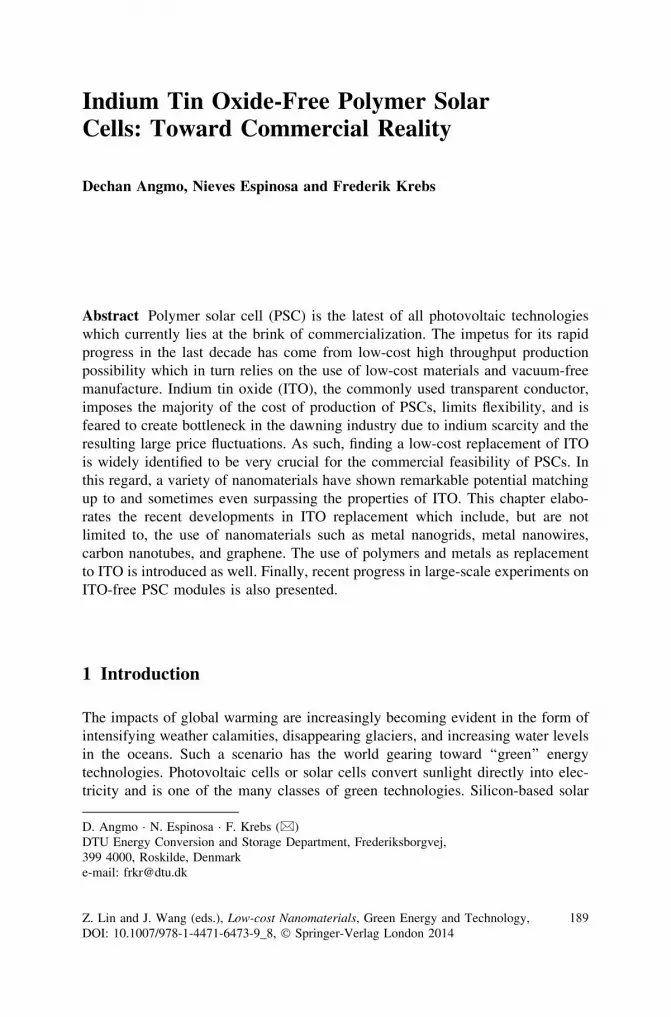
cells is the most known and the oldest photovoltaic technology; there are, however,a plethora of non-silicon-based solar cells in the market or under developmenttoday. Solar cells can be generally divided into two broad categories depending onthe type of the photoactive material: inorganic and organic solar cells (Fig. 1).Among the inorganic solar cells are the first generation solar cells based on siliconand the second generation solar cells based on thin films of amorphous silicon(a-Si) and on chalcogenides such as CdSe, CIGS, CdTe, etc. Organic solar cellsform the third generation of photovoltaic technology. Organic solar cells can befurther demarcated into three subdivisions: dye sensitized, small molecules, andpolymer solar cells. Polymer solar cells (PSCs) are the most recent technology andthis chapter is focused on PSCs.
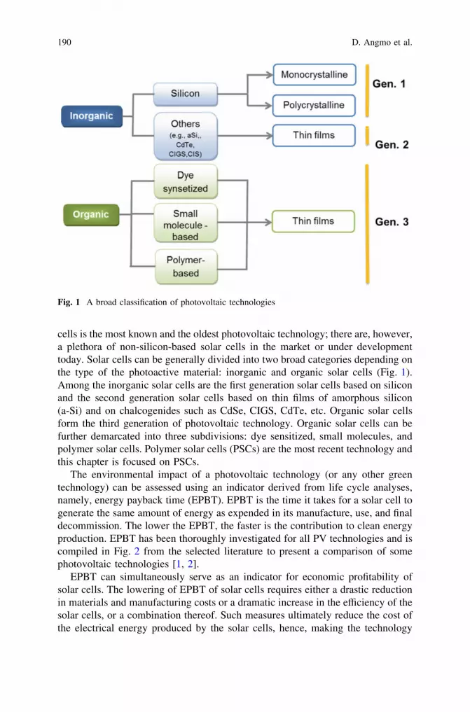
The environmental impact of a photovoltaic technology (or any other greentechnology) can be assessed using an indicator derived from life cycle analyses,namely, energy payback time (EPBT). EPBT is the time it takes for a solar cell togenerate the same amount of energy as expended in its manufacture, use, and finaldecommission. The lower the EPBT, the faster is the contribution to clean energyproduction. EPBT has been thoroughly investigated for all PV technologies and iscompiled in Fig. 2 from the selected literature to present a comparison of somephotovoltaic technologies [1, 2].
EPBT can simultaneously serve as an indicator for economic profitability ofsolar cells. The lowering of EPBT of solar cells requires either a drastic reductionin materials and manufacturing costs or a dramatic increase in the efficiency of thesolar cells, or a combination thereof. Such measures ultimately reduce the cost ofthe electrical energy produced by the solar cells, hence, making the technology
Fig. 1 A broad classification of photovoltaic technologies
190 D. Angmo et al.
more economically competitive. Since most mature solar cells already operate ator near theoretically permissible efficiencies, the need for cost reduction inmaterials and processing has driven the development of solar cell technology fromthe first to the third generation.
The first generation of monocrystalline silicon is grown in the form of ingotsvia the Czochralski process that requires Si to be in molten form which is achievedat [1400 �C. The EPBT of [2 years for such cells despite its high efficiency andlifetime clearly indicates the relatively exorbitant energy investment that the firstgeneration PV requires in comparison to other technologies (Fig. 2). The need tocompensate such a slow and high energy input processing led to the developmentof second generation solar cells. The latter could be produced faster using tech-niques such as sputtering and chemical vapor deposition routes and employingcheaper materials albeit at a cost to performance.
The third generation of organic solar cells is pursued, despite the relativelylower expected efficiency and lifetime in comparison to the former generations,primarily because of their potential at drastic reduction in materials and productioncost. Such a potential is envisioned accomplishable through high throughput roll-to-roll production with coating and printing at low temperatures that commonplastic substrates such as PET can withstand (\140 �C). The initial experiments onlarge-area indium tin oxide (ITO)-based PSC modules produced by complete roll-to-roll production [3, 4] and their subsequent cost analyses [1] revealed that the useof ITO is not feasible in the low-cost production of PSCs. ITO is a commonly used
Fig. 2 Energy payback time for PV modules technologies. South Mediterranean irradiance(1,700 kWh/m2/year) and a performance ratio of 0.8 are assumed. The module efficiency is shownin brackets. DS stands for dye sensitized modules and A and B refer to the low and high values ofthe energy range. Process One is ITO-based PSCs, Process H is ITO-free PSCs, SFE is metal- andITO-free PSCs
Indium Tin Oxide-Free Polymer Solar Cells 191
transparent conductor directly adapted from other optoelectronic applications ingeneral and inorganic solar cells in particular. It has high conductivity (sheetresistance of 10–20 X !-1) and transmission ([80 %) in the visible region of theelectromagnetic spectrum. However, the processing of ITO requires high prepa-ration temperatures and vacuum-based highly energy-intensive and throughputlimiting deposition techniques such as sputtering while all other components inPSCs can be coated and printed in ambient conditions. As a result, the costfootprint of ITO in PSCs is much larger than in inorganic solar cells. In fact, costanalyses [3, 5, 6] suggest that ITO accounts for [50 % of the total cost of a PSCmodule. Life cycle analyses of R2R-produced ITO-based PSC modules reveal thatITO on PET substrate accounts for *90 % of the total energy (embodied energyand direct process energy) imposed by all input raw materials [1]. Furthermore, thebrittle nature of ITO is not conducive for application on flexible substrates that areprone to bending and flexing and may inevitably lead to deterioration in theperformance of PSCs. Lastly, the scarcity of indium resources in the world and itshigh demand from the display industry has created large cost fluctuations andfuture supply concerns. All these factors substantiate the need for finding a cost-effective alternative to ITO that ideally involves no challenges with scarcity andcan be processed in a vacuum-free environment. Such an alternative would sig-nificantly improve the environmental and commercial feasibility of PSCtechnology.
Following a brief overview on PSCs, this chapter lays out the different alter-natives of ITO that are widely researched. Each alternative is introduced alongwith the current development in their application in PSCs. Particular emphasis islaid on the implications of the processing choices of fabrication of ITO alternativeson the solar cell performance and suitability for low-cost upscaling. At the end ofthe chapter, a subsection is presented with recent progress on ITO-free roll-to-rollprocessed PSC modules.
2 Polymer Solar Cells: A Brief Overview
2.1 Device Structure
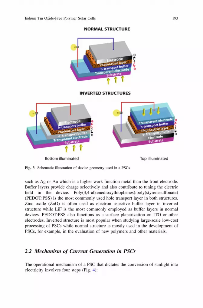
A polymer solar cell comprises of a thin film of the photoactive material sand-wiched between two electrodes of different work functions. One of the electrodesis a transparent conductor from where light is permitted to the photoactive layer.Two different architectures are commonly used: a normal structure and an invertedstructure (Fig. 3). In normal structure, holes are collected at the front electrode—the transparent conductor—while electrons are collected at the back electrodewhich is a lower work-function metal (usually Al) than the front electrode. Ininverted structure, the reverse process takes place, that is, the electrons are col-lected by the transparent conductor and holes are collected by the back electrode
192 D. Angmo et al.
such as Ag or Au which is a higher work function metal than the front electrode.Buffer layers provide charge selectively and also contribute to tuning the electricfield in the device. Poly(3,4-alkenedioxythiophenes):poly(styrenesulfonate)(PEDOT:PSS) is the most commonly used hole transport layer in both structures.Zinc oxide (ZnO) is often used as electron selective buffer layer in invertedstructure while LiF is the most commonly employed as buffer layers in normaldevices. PEDOT:PSS also functions as a surface planarization on ITO or otherelectrodes. Inverted structure is most popular when studying large-scale low-costprocessing of PSCs while normal structure is mostly used in the development ofPSCs, for example, in the evaluation of new polymers and other materials.
2.2 Mechanism of Current Generation in PSCs
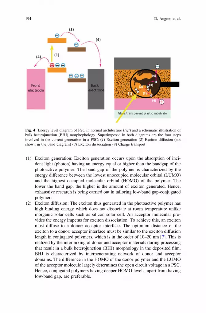
The operational mechanism of a PSC that dictates the conversion of sunlight intoelectricity involves four steps (Fig. 4):
Fig. 3 Schematic illustration of device geometry used in a PSCs
Indium Tin Oxide-Free Polymer Solar Cells 193
(1) Exciton generation: Exciton generation occurs upon the absorption of inci-dent light (photon) having an energy equal or higher than the bandgap of thephotoactive polymer. The band gap of the polymer is characterized by theenergy difference between the lowest unoccupied molecular orbital (LUMO)and the highest occupied molecular orbital (HOMO) of the polymer. Thelower the band gap, the higher is the amount of exciton generated. Hence,exhaustive research is being carried out in tailoring low-band gap-conjugatedpolymers.
(2) Exciton diffusion: The exciton thus generated in the photoactive polymer hashigh binding energy which does not dissociate at room temperature unlikeinorganic solar cells such as silicon solar cell. An acceptor molecular pro-vides the energy impetus for exciton dissociation. To achieve this, an excitonmust diffuse to a donor: acceptor interface. The optimum distance of theexciton to a donor: acceptor interface must be similar to the exciton diffusionlength in conjugated polymers, which is in the order of 10–20 nm [7]. This isrealized by the intermixing of donor and acceptor materials during processingthat result in a bulk heterojunction (BHJ) morphology in the deposited film.BHJ is characterized by interpenetrating network of donor and acceptordomains. The difference in the HOMO of the donor polymer and the LUMOof the acceptor molecule largely determines the open circuit voltage in a PSC.Hence, conjugated polymers having deeper HOMO levels, apart from havinglow-band gap, are preferable.
Fig. 4 Energy level diagram of PSC in normal architecture (left) and a schematic illustration ofbulk heterojunction (BHJ) morphophology. Superimposed in both diagrams are the four stepsinvolved in the current generation in a PSC: (1) Exciton generation (2) Exciton diffusion (notshown in the band diagram) (3) Exciton dissociation (4) Charge transport
194 D. Angmo et al.
(3) Exciton dissociation: At the donor: acceptor interface, the exciton dissociatesforming free charge carriers.
(4) Charge transport: Once free charge carriers are generated, they are trans-ported to their respective electrodes according to the electric field in thedevice. The holes and electrons travel through the percolated network ofdonor and acceptor, respectively. Once collected by the electrodes, they arechanneled into the external circuit.
Poly(3-hexylthiophene-2,5-diyl (P3HT) and [6,6]-phenyl-C61-butyric acidmethyl ester (PCBM) are extensively studied and commonly used donor polymerand acceptor molecule, respectively. A comprehensive overview of all photoactivepolymers and acceptor molecules could be found elsewhere [8, 9]. Similarly,several reviews could be consulted for deeper understanding of device physics ofPSCs [7, 10, 11].
2.3 Photovoltaic Characterization
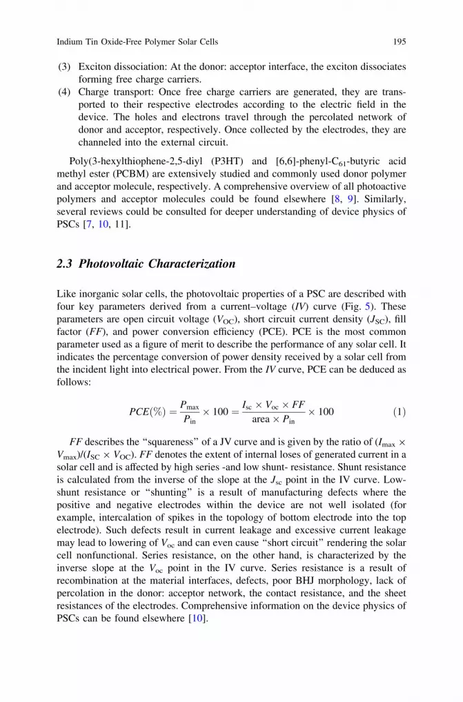
Like inorganic solar cells, the photovoltaic properties of a PSC are described withfour key parameters derived from a current–voltage (IV) curve (Fig. 5). Theseparameters are open circuit voltage (VOC), short circuit current density (JSC), fillfactor (FF), and power conversion efficiency (PCE). PCE is the most commonparameter used as a figure of merit to describe the performance of any solar cell. Itindicates the percentage conversion of power density received by a solar cell fromthe incident light into electrical power. From the IV curve, PCE can be deduced asfollows:
PCE %ð Þ ¼ Pmax
Pin
� 100 ¼ Isc � Voc � FF
area� Pin
� 100 ð1Þ
FF describes the ‘‘squareness’’ of a JV curve and is given by the ratio of (Imax 9
Vmax)/(ISC 9 VOC). FF denotes the extent of internal loses of generated current in asolar cell and is affected by high series -and low shunt- resistance. Shunt resistanceis calculated from the inverse of the slope at the Jsc point in the IV curve. Low-shunt resistance or ‘‘shunting’’ is a result of manufacturing defects where thepositive and negative electrodes within the device are not well isolated (forexample, intercalation of spikes in the topology of bottom electrode into the topelectrode). Such defects result in current leakage and excessive current leakagemay lead to lowering of Voc and can even cause ‘‘short circuit’’ rendering the solarcell nonfunctional. Series resistance, on the other hand, is characterized by theinverse slope at the Voc point in the IV curve. Series resistance is a result ofrecombination at the material interfaces, defects, poor BHJ morphology, lack ofpercolation in the donor: acceptor network, the contact resistance, and the sheetresistances of the electrodes. Comprehensive information on the device physics ofPSCs can be found elsewhere [10].
Indium Tin Oxide-Free Polymer Solar Cells 195
3 Alternatives to ITO
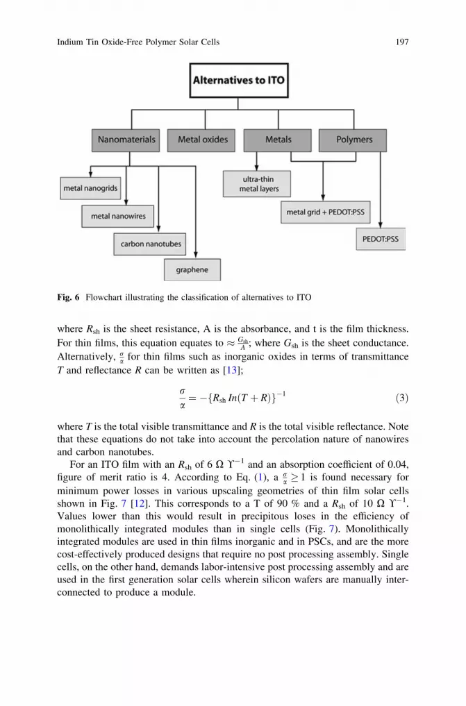
Indium tin oxide is a ubiquitous material in most optoelectronic devices and assuch the efforts in finding an alternative to ITO is exhaustive. In general, thealternatives of ITO could be categorized into four broad material groups: (1)nanomaterials; (2) polymers; (3) metals; and (4) metal oxides. Nanomaterials canfurther be classified into carbon nanotubes, graphene, metal nanowires, and metalnanogrids. These material groups are not mutually exclusive and are often used insome combination with each other. Particularly, Poly(3,4-ethylenedioxythio-phene):poly(styrenesulfonate) or PEDOT:PSS often used in combination withmany of these alternatives. Figure 6 summaries material categories that areinvestigated as alternatives to ITO.
When evaluating the efficacy of transparent conductors for application in solarcells, two property parameters are of prime importance: optical transparency andsheet resistance (Rsh). However, these parameters are often in competition withone another and an improvement in one often requires a sacrifice in the other.
Commercially available ITO usually has an Rsh of 10 X !-1 and a visibletransmittance of [80 %. Such a property of ITO is used as a benchmark againstwhich alternatives are being developed and assessed. A figure of merit relationshipthat enables property comparison between different transparent conductors is theratio between DC conductivity (r) and absorptivity (a) which is given by [12];
ra¼
1t�Rsh
� lnð1�AÞt
ð2Þ
Fig. 5 Current–voltagecurve of a solar cell in darkand under illumination
196 D. Angmo et al.
where Rsh is the sheet resistance, A is the absorbance, and t is the film thickness.For thin films, this equation equates to � Gsh
A ; where Gsh is the sheet conductance.Alternatively, r
a for thin films such as inorganic oxides in terms of transmittanceT and reflectance R can be written as [13];
ra¼ � Rsh In T þ Rð Þf g�1 ð3Þ
where T is the total visible transmittance and R is the total visible reflectance. Notethat these equations do not take into account the percolation nature of nanowiresand carbon nanotubes.
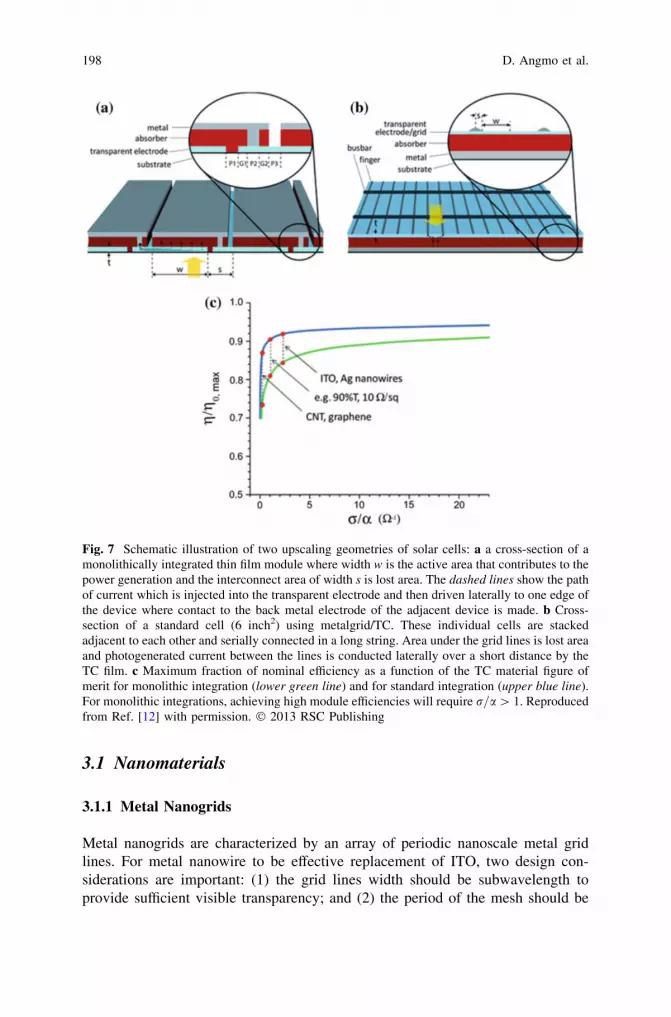
For an ITO film with an Rsh of 6 X !-1 and an absorption coefficient of 0.04,figure of merit ratio is 4. According to Eq. (1), a r
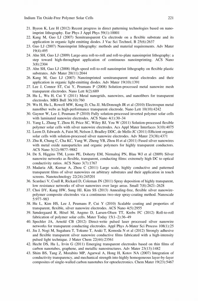
a � 1 is found necessary forminimum power losses in various upscaling geometries of thin film solar cellsshown in Fig. 7 [12]. This corresponds to a T of 90 % and a Rsh of 10 X !-1.Values lower than this would result in precipitous loses in the efficiency ofmonolithically integrated modules than in single cells (Fig. 7). Monolithicallyintegrated modules are used in thin films inorganic and in PSCs, and are the morecost-effectively produced designs that require no post processing assembly. Singlecells, on the other hand, demands labor-intensive post processing assembly and areused in the first generation solar cells wherein silicon wafers are manually inter-connected to produce a module.
Fig. 6 Flowchart illustrating the classification of alternatives to ITO
Indium Tin Oxide-Free Polymer Solar Cells 197
3.1 Nanomaterials
3.1.1 Metal Nanogrids
Metal nanogrids are characterized by an array of periodic nanoscale metal gridlines. For metal nanowire to be effective replacement of ITO, two design con-siderations are important: (1) the grid lines width should be subwavelength toprovide sufficient visible transparency; and (2) the period of the mesh should be
Fig. 7 Schematic illustration of two upscaling geometries of solar cells: a a cross-section of amonolithically integrated thin film module where width w is the active area that contributes to thepower generation and the interconnect area of width s is lost area. The dashed lines show the pathof current which is injected into the transparent electrode and then driven laterally to one edge ofthe device where contact to the back metal electrode of the adjacent device is made. b Cross-section of a standard cell (6 inch2) using metalgrid/TC. These individual cells are stackedadjacent to each other and serially connected in a long string. Area under the grid lines is lost areaand photogenerated current between the lines is conducted laterally over a short distance by theTC film. c Maximum fraction of nominal efficiency as a function of the TC material figure ofmerit for monolithic integration (lower green line) and for standard integration (upper blue line).For monolithic integrations, achieving high module efficiencies will require r=a[ 1. Reproducedfrom Ref. [12] with permission. � 2013 RSC Publishing
198 D. Angmo et al.
submicrometer to ensure uniformity of charge collection in any device [14]. Such aperiodic array of metal grid lines enables light scattering and coupling, therefore,enhancing photon flux to the photoactive material [15]. Unlike in ITO wheretransparency and conductivity are competing parameters, conductivity in nanometal grids can be improved by increasing the line height without increasing thewidth of the grid lines and therefore avoiding decrease in transmittance due toshading from the grid lines. The relationship of the Rsh of a periodic array of metalgrid to physical attributes of the grid lines can be deducted from Kirchoff’s rule.Assuming a square wire network with N 9 N wires, Rsh is given by;
Rsh ¼N
N þ 1qL
whð3Þ
where q is the wire resistivity, L is the wire length, w is the wire width, and h is thewire height [16].
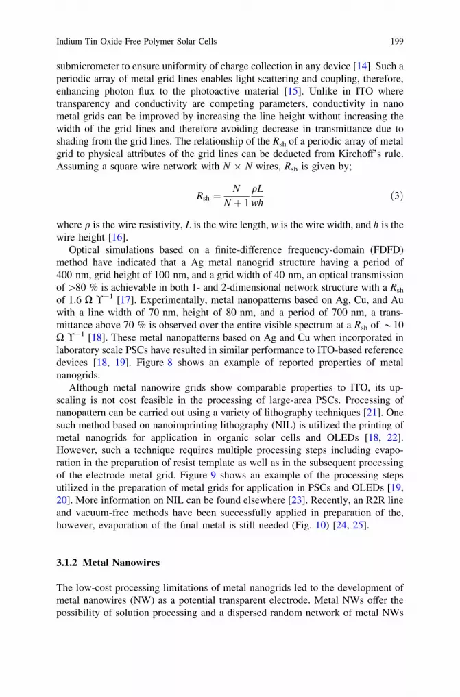
Optical simulations based on a finite-difference frequency-domain (FDFD)method have indicated that a Ag metal nanogrid structure having a period of400 nm, grid height of 100 nm, and a grid width of 40 nm, an optical transmissionof [80 % is achievable in both 1- and 2-dimensional network structure with a Rsh
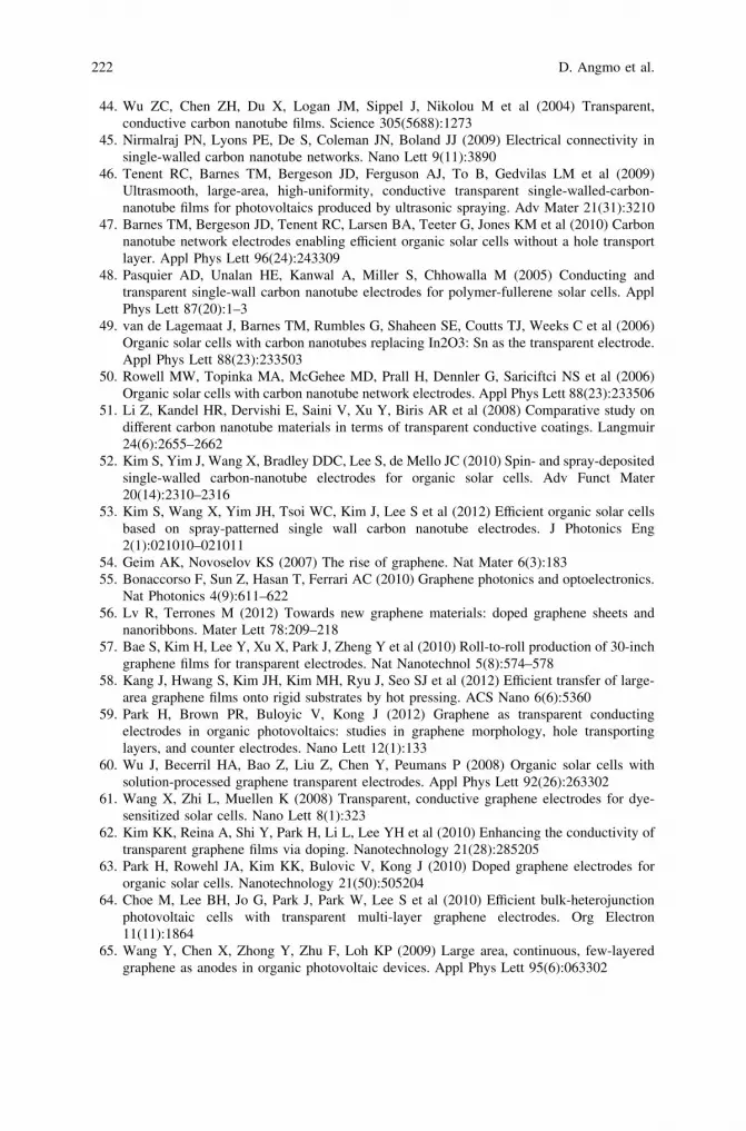
of 1.6 X !-1 [17]. Experimentally, metal nanopatterns based on Ag, Cu, and Auwith a line width of 70 nm, height of 80 nm, and a period of 700 nm, a trans-mittance above 70 % is observed over the entire visible spectrum at a Rsh of *10X !-1 [18]. These metal nanopatterns based on Ag and Cu when incorporated inlaboratory scale PSCs have resulted in similar performance to ITO-based referencedevices [18, 19]. Figure 8 shows an example of reported properties of metalnanogrids.
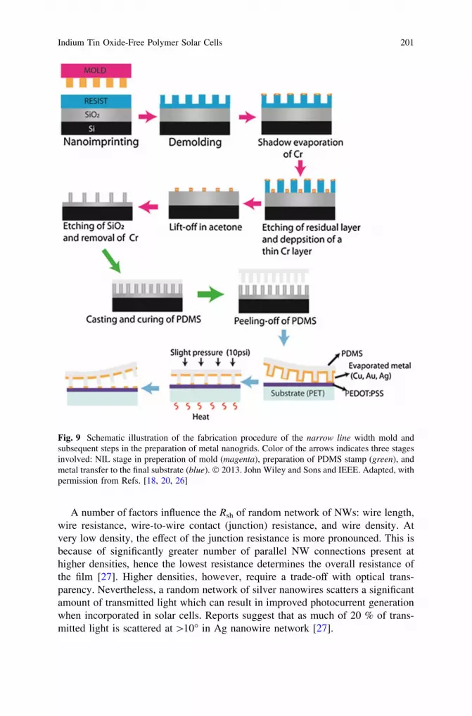
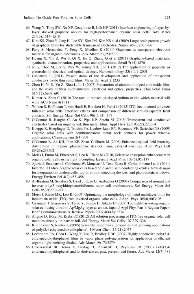
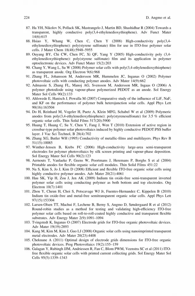
Although metal nanowire grids show comparable properties to ITO, its up-scaling is not cost feasible in the processing of large-area PSCs. Processing ofnanopattern can be carried out using a variety of lithography techniques [21]. Onesuch method based on nanoimprinting lithography (NIL) is utilized the printing ofmetal nanogrids for application in organic solar cells and OLEDs [18, 22].However, such a technique requires multiple processing steps including evapo-ration in the preparation of resist template as well as in the subsequent processingof the electrode metal grid. Figure 9 shows an example of the processing stepsutilized in the preparation of metal grids for application in PSCs and OLEDs [19,20]. More information on NIL can be found elsewhere [23]. Recently, an R2R lineand vacuum-free methods have been successfully applied in preparation of the,however, evaporation of the final metal is still needed (Fig. 10) [24, 25].
3.1.2 Metal Nanowires
The low-cost processing limitations of metal nanogrids led to the development ofmetal nanowires (NW) as a potential transparent electrode. Metal NWs offer thepossibility of solution processing and a dispersed random network of metal NWs
Indium Tin Oxide-Free Polymer Solar Cells 199
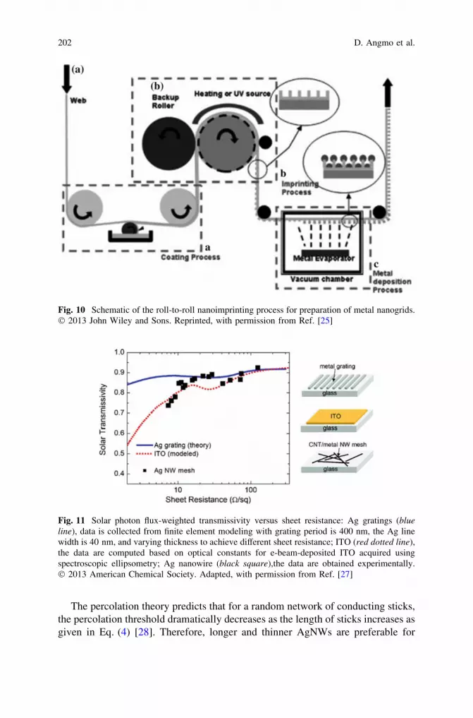
can exhibit transmission and conductivity even superior to ITO. Figure 11 shows acomparison the relationship between transmittance and Rsh in ITO, metalnanogrids, and metal nanowires. In metal oxide transparent conductors such asITO, there is an inherent trade off between Rsh and transparency which is deter-mined by film thickness. While higher film thicknesses allow lower Rsh, however,at a significant loss of transparency. Calculations on ITO have shown that theoptical transparency of ITO suffers greatly with increasing film thicknessesparticularly below Rsh of 15 X !-1 [27]. In case of metal nanogrids, we haveearlier noted that the Rsh can be improved at no cost to optical transparency byincreasing grid height and maintaining the line width. Experimental results onmetal nanowires indicate that a random network film of Ag nanowires exhibitcomparable properties to either ITO or metal grids. At the same time, the solutionprocessing possibility of metal nanowire marks its competitive edge over ITO andnanogrids in the low-cost processing.
Fig. 8 a Optical transmittance of nanogrids (line width 70 nm and period 700 nm) madedifferent metals; b IV characteristic of PSCs incorporating metal nanogrid transparent electrodewith the structure: transparent grid/PEDOT:PSS/P3HT:PCBM/LiF/Al. c Average transmittanceversus sheet resistance of metal grids with a line width of 120 nm. d Scanning electronmicroscopy image of an as-fabricated metal nanogrid electrode with a line width of 70 nm and aperiod of 700 nm. � 2013. John Wiley and Sons and IEEE. Reprinted, with permission fromRefs. [18, 20, 26]
200 D. Angmo et al.
A number of factors influence the Rsh of random network of NWs: wire length,wire resistance, wire-to-wire contact (junction) resistance, and wire density. Atvery low density, the effect of the junction resistance is more pronounced. This isbecause of significantly greater number of parallel NW connections present athigher densities, hence the lowest resistance determines the overall resistance ofthe film [27]. Higher densities, however, require a trade-off with optical trans-parency. Nevertheless, a random network of silver nanowires scatters a significantamount of transmitted light which can result in improved photocurrent generationwhen incorporated in solar cells. Reports suggest that as much of 20 % of trans-mitted light is scattered at [10� in Ag nanowire network [27].
Fig. 9 Schematic illustration of the fabrication procedure of the narrow line width mold andsubsequent steps in the preparation of metal nanogrids. Color of the arrows indicates three stagesinvolved: NIL stage in preperation of mold (magenta), preparation of PDMS stamp (green), andmetal transfer to the final substrate (blue). � 2013. John Wiley and Sons and IEEE. Adapted, withpermission from Refs. [18, 20, 26]
Indium Tin Oxide-Free Polymer Solar Cells 201
The percolation theory predicts that for a random network of conducting sticks,the percolation threshold dramatically decreases as the length of sticks increases asgiven in Eq. (4) [28]. Therefore, longer and thinner AgNWs are preferable for
Fig. 10 Schematic of the roll-to-roll nanoimprinting process for preparation of metal nanogrids.� 2013 John Wiley and Sons. Reprinted, with permission from Ref. [25]
Fig. 11 Solar photon flux-weighted transmissivity versus sheet resistance: Ag gratings (blueline), data is collected from finite element modeling with grating period is 400 nm, the Ag linewidth is 40 nm, and varying thickness to achieve different sheet resistance; ITO (red dotted line),the data are computed based on optical constants for e-beam-deposited ITO acquired usingspectroscopic ellipsometry; Ag nanowire (black square),the data are obtained experimentally.� 2013 American Chemical Society. Adapted, with permission from Ref. [27]
202 D. Angmo et al.
optimizing transparency and Rsh of a random of NWs. Processing methods aresought to produce nanowires of longer length. The use of electro spinning, forexample, could produce ultra-long metal wires (nanofibers). Such nanofibers of Cufilms have been demonstrated to exhibit similar Rsh and transmittance as ITO films:
Nc ¼1p
4:236L
� �2
ð4Þ
where Nc is the percolation threshold and L is length of the sticks [29].Nanowire films, however, have a drawback. When incorporated in solar cells in
the normal device architecture (Fig. 3), the high roughness leads to interpenetra-tion of the nanowires to the counter electrodes leading to large dark currentleakage or even short circuit. The roughness of the NW film can exceed the layerthickness of the overlying photoactive materials (50–200 nm). Several processingstrategies have been explored to passivate the surface roughness of NW films.First, an alternate inverted structure, the top illuminated inverted device in Fig. 3,is often employed in which NWs are laminated onto PEDOT:PSS layer. Such astructure alleviates the problem of shunting due to roughness although completeelimination is seldom accomplished. With the use of a short pulse high voltage toburn the remaining shunts, a working module with the structure substrate/Ag film/Cs2O3/P3HT:PCBM/PEDOT:PSS/AgNW has shown a PCE of 2.5 %; Jsc:10.59 mA/cm2; Voc: 0.51 V, and FF: 46 % on a device area of 2 mm2 [30]. Incontrast, AgNW transparent conductors in a P3HT:PCBM-based solar cell in anormal architecture showed a PCE of 1.1 % with significantly lower Voc than ITO-based reference devices [31]. Second, in a bottom illuminated inverted device, theproblem of roughness can be circumvented by increasing the thickness of thebuffer layer. Increasing TiO2 thickness in a device structure substrate/AgNW/TiO2/P3HT:PCBM/Mo2O3/Ag has shown a PCE of 3.42 %; Jsc:10.1 mA/cm2; Voc
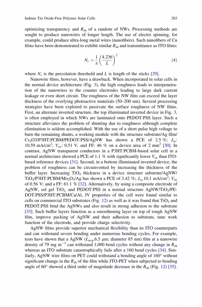
of 0.56 V; and a FF: 61.1 % [32]. Alternatively, by using a composite electrode ofAgNW, sol gel TiO2, and PEDOT:PSS in a normal structure AgNW/TiO2/PE-DOT:PSS/P3HT:PCBM/Ca/Al, JV properties of the cell were found similar tocells on commercial ITO substrates (Fig. 12) as well as it was found that TiO2 andPEDOT:PSS bind the AgNWs and also result in strong adhesion to the substrate[33]. Such buffer layers function as a smoothening layer on top of rough AgNWfilm, improve packing of AgNW and their adhesion to substrate, tune workfunction of the electrode, and provide charge selectivity.
AgNW films provide superior mechanical flexibility than its ITO counterpartsand can withstand severe bending under numerous bending cycles. For example,tests have shown that a AgNW (Lavg.6.5 lm; diameter 85 nm) film at a nanowiredensity of 79 mg m-2 can withstand 1,000 bend cycles without any change in Rsh
whereas an ITO substrate catastrophically fails after a 160 bend cycles [34]. Sim-ilarly, AgNW wire films on PET could withstand a bending angle of 160� withoutsignificant change in the Rsh of the film while ITO-PET when subjected to bendingangle of 60� showed a third order of magnitude decrease in the Rsh (Fig. 12) [35].
Indium Tin Oxide-Free Polymer Solar Cells 203
Research on metal nanowires is very recent. So far, studies on NW films haveaffirmed its applicability as an effective replacement to ITO. Currently, research onmetal nanowires is slowly gearing toward finding large-scale compatible tech-niques. In early reports, metal NW films were processed by drop casting a sus-pension of surfactant-assisted dispersed AgNW, followed by annealing [27, 30].Such a processing method is not scalable and cannot generate uniform films overlarge area. As such, these films were less than a cm2 of area. Spray-coating is ascalable technique that has been recently employed in the preparation of large-areaAgNW transparent substrates [36, 37]. A composite AgNW and PEDOT:PSS, bothspray coated consecutively have demonstrated low roughness and a Rsh of 10 X!-1 with a mean optical transmittance of 85 % without any annealing steps [37].
Fig. 12 a Photograph of a silver nanowire film deposited on a *2 9 2 cm PET substrate with T80 % and Rsh 25 X !-1; b SEM image of the percolating nanowire distribution of the sampleshown in a; c IV curve of P3HT:PCBM cells on ITO or AgNW/TiO2/PEDOT:PSS substrates; d Aplot of Rsh versus bending angle of two Ag nanowire films deposited on PET with transmittancevalues of 60 and 80 %. The solid lines represent the change in sheet resistance during bendingand the dotted lines represent the change in sheet resistance during unbending. TheAg nanowirefilm remains conductive even under severe bending. (a, b, and d) reprinted from Ref. [35] � IOPPublishing, 2013. Reproduced with permission from IOP Publishing. All rights reserved. c �2013 Amercian Chemical Society. Reprinted, with permission from Ref. [33]
204 D. Angmo et al.
Other methods include Meyer rod coating in which a metal nanowire suspension isplaced on the substrate and a Meyer rod is pulled over it. Using this method, an8 9 8 inch substrate has been prepared [38].
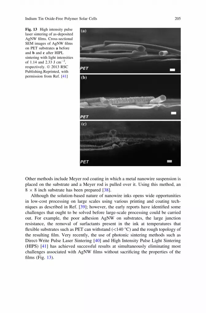
Although the solution-based nature of nanowire inks opens wide opportunitiesin low-cost processing on large scales using various printing and coating tech-niques as described in Ref. [39]; however, the early reports have identified somechallenges that ought to be solved before large-scale processing could be carriedout. For example, the poor adhesion AgNW on substrates, the large junctionresistance, the removal of surfactants present in the ink at temperatures thatflexible substrates such as PET can withstand (\140 �C) and the rough topology ofthe resulting film. Very recently, the use of photonic sintering methods such asDirect-Write Pulse Laser Sintering [40] and High Intensity Pulse Light Sintering(HIPS) [41] has achieved successful results at simultaneously eliminating mostchallenges associated with AgNW films without sacrificing the properties of thefilms (Fig. 13).
Fig. 13 High intensity pulselaser sintering of as-depositedAgNW films. Cross-sectionalSEM images of AgNW filmson PET substrates a beforeand b and c after HIPLsintering with light intensitiesof 1.14 and 2.33 J cm-2,respectively. � 2013 RSCPublishing.Reprinted, withpermission from Ref. [41]
Indium Tin Oxide-Free Polymer Solar Cells 205
3.1.3 Carbon Nanotubes
It was not too long after the first report on carbon nanotubes in 1991 by SumioIIjima that the excellent mechanical, electrical, and optical properties of carbonnanotubes were identified. Theoretically, single-wall carbon nanotubes (SWCNTs)can have a current conductivity up to 1–3 106 S m-1 and mobility of 100,000 cm2
V-1 s-1 [42, 43]. In films, a random network of CNTs possess far lower con-ductivity and mobility than a single tube primarily due to the presence of highjunction resistance as well as due to a large number of parameters that affect CNTconductivity and mobility such as purity, lattice perfection, bundle size, wallnumber, metal/semiconductor ratio, diameter, length, and doping level. Nonethe-less, conductivity up to 6,600 SCM-1 and mobility up to 10 cm2 V-2 is experi-mentally observed in films [42]. As a result, a wide variety of advancedapplications have been envisioned for CNTs; transparent conductors being one ofthem.
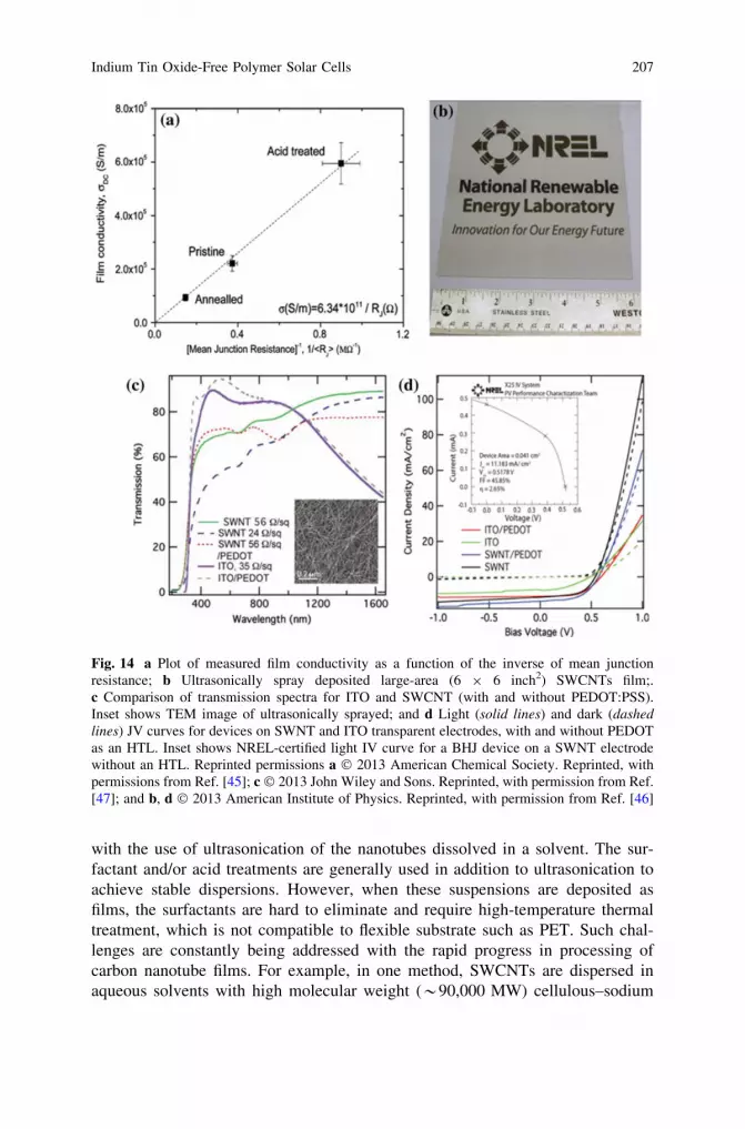
An early report noted that a 50 nm thin film of p-doped SWNT film has a Rsh of30 X !-1 with a transmission of [70 % over visible region of the light spectrum[44]. However, accomplishing such results in subsequent reports has not been easydue to the large number of parameters involved. Much like nanowires, the Rsh ofCNT films is dominated by junction resistance. The use of doping by acid treat-ments has been shown to cause a threefold decrease in junction resistance and a30 % increase in the nanotube conductivity when compared to pristine untreatedsamples [45] (Fig. 14). For example, acid treatment of CNTs has resulted inimprovement in Rsh of spray-coated SWCNT film from 110 X !-1 (pristineSWCNT) to 37 X !-1 (doped SWCNT) with transmittance of 78 and 76 %(550 nm) respectively (Fig. 14) [46].
Apart from the large junction resistance, the roughness of the CNTs thin filmsand their adhesion to the substrates has been equally impeding factors to theirefficacy in organic solar cells. Such issues are similar to those observed innanowire-based transparent conductors as well. Shunts due to roughness of theSWCNT surface is circumvented, for example, by either using thick active layer(0.5–1 lm thick) or using a planarization layer such as PEDOT:PSS, or both [48,49]. Other approaches include, for example, the application of pressure upontransferring of dispersed named with a PDMS stamp [50]. Using such a method, alow roughness value of 10 nm over a scan area of 25 lm2 was observed in anuntreated SWCNT-based film. When the film is used in the fabrication of PSCs, aPCE of 2.5 % was attained. With the use of doped SWCNT, such a transfermethod will likely yield similar performance to ITO (PCE 3 %).
The earlier reports were generally proof of principle studies wherein upscalingcompatibility of processing was not the central concern. With the promising resultsshown by these proof of principle studies, recently, reports on large-scale com-patible processing have emerged. Spray coating is recently investigated in thepreparation of large-area CNT transparent film on PET substrate [46, 47, 51, 52].Generally, CNTs are processed from suspensions in a solvent. High van der Waalsforces render the nanotubes very susceptible to bundling. De-bundling is achieved
206 D. Angmo et al.
with the use of ultrasonication of the nanotubes dissolved in a solvent. The sur-factant and/or acid treatments are generally used in addition to ultrasonication toachieve stable dispersions. However, when these suspensions are deposited asfilms, the surfactants are hard to eliminate and require high-temperature thermaltreatment, which is not compatible to flexible substrate such as PET. Such chal-lenges are constantly being addressed with the rapid progress in processing ofcarbon nanotube films. For example, in one method, SWCNTs are dispersed inaqueous solvents with high molecular weight (*90,000 MW) cellulous–sodium
Fig. 14 a Plot of measured film conductivity as a function of the inverse of mean junctionresistance; b Ultrasonically spray deposited large-area (6 9 6 inch2) SWCNTs film;.c Comparison of transmission spectra for ITO and SWCNT (with and without PEDOT:PSS).Inset shows TEM image of ultrasonically sprayed; and d Light (solid lines) and dark (dashedlines) JV curves for devices on SWNT and ITO transparent electrodes, with and without PEDOTas an HTL. Inset shows NREL-certified light IV curve for a BHJ device on a SWNT electrodewithout an HTL. Reprinted permissions a � 2013 American Chemical Society. Reprinted, withpermissions from Ref. [45]; c � 2013 John Wiley and Sons. Reprinted, with permission from Ref.[47]; and b, d � 2013 American Institute of Physics. Reprinted, with permission from Ref. [46]
Indium Tin Oxide-Free Polymer Solar Cells 207
carboxymethylcellulose (CMC)—as a dispersing agent and an ultrasonic sprayingis used to deposit the film over large area (6 9 6 inch). Once deposited, theSWCNTs are doped by exposing the film to nitric acid which simultaneouslyeliminates CMC. Such a film is found to be highly homogenous (rms roughness of3 nm scanned over 100 lm2 area) and have resulted in a Rsh of 60 X !-1 at atransmission of 60–70 % (at 550 nm). PSCs with the structure SWCNT/PE-DOT:PSS/P3HT:PCBM/Ca/Al fabricated on such a film have resulted in a PCE of3.1 % which is close to reference device with ITO substrate that demonstrated aPCE of 3.6 % [46]. Unlike in other devices where the main function of PE-DOT:PSS is providing charge selective transportation as a buffer layer, it has beenobserved that in SWCNT-based PSC devices does not require a charge selectivePEDOT:PSS buffer layer in normal devices. In fact, the elimination of PEDOT:PSS results in superior PCE because of improvement in optical transmission to thephotoactive material (Fig. 14). Nonetheless, PEDOT: PSS provides a planarizationlayer suppressing the intercalation of nanotubes into the counter electrodes. Theelimination of PEDOT: PSS requires increasing thickness of the active layer inorder to prevent electrical shorts due to roughness in the surface of CNT film [47].The transparent films of CNTs have higher transmission beyond the visible regionand are suggested to generate higher current density than theoretical predictionsthat are based on transmission in the visible range (Fig. 14). So far, the highestreported PCE of P3HT:PCBM-based PSCs with SWCNTs transparent conductorsis 3.6 and 2.6 % on glass and PET substrates, respectively [53].
The adhesion of nanotubes on surface of a substrate is yet another processingchallenge. Recent advancement in this regard includes the application of 1 %solution of 3-aminopropyltriethoxy silane on the substrate which has been found toimprove the adhesion of SWCNTs onto the substrates due to the formation ofcross-linked siloxane on the surface of substrates.
It has been a decade since the application of CNTs as transparent conductorswere recognized, however progress has been slow primarily owing to the chal-lenges in processing. There is a long way before SWCNTs transparent conductorscan make their way into R2R processing. Reports thus far have demonstrated proofof principle and the task ahead is to demonstrate a robust processing technique(s)that is feasible for application in the processing of PSCs and is easily scalable.
3.1.4 Graphene
Graphene is a two-dimensional material consisting of a monolayer of sp2-hybridized carbon atoms resulting in a hexagonal arrangement. A monolayer ofgraphene theoretically would exhibit a reflectance of less than 0.1 % and anabsorbance of 2.3 %, therefore resulting in a theoretical transmission limit of97.7 %. However, graphene is a zero band gap semiconductor and undopedgraphene sheet has high Rsh values of 6 kX !-1 [54, 55]. Doping is an efficientmethod that allows tailoring of various properties of graphene and can be carriedout following various chemical and electrical routes [56]. So far, a Rsh of 30 X !-1
208 D. Angmo et al.
and a corresponding transmission of 90 % has been observed in doped graphenesheets, thus making graphene potentially suitable as transparent conductors [57].Apart from Rsh and transmission, several other properties such as the highchemical and thermal stability, high charge carrier mobility (200 cm2 V-1 s-1),high current carrying capacity (3 9 108 A cm-2), high stretchability, and low-contact resistance with organic materials render graphene a very favorable alter-native to ITO [58, 59].
In principle, a monolayer of graphene possesses ballistic charge transport due todelocalization of electrons over the complete sheet, however, in practice defectsare introduced during growth and processing of graphene. Such defects, forexample, lattice defects, grain boundaries, and oxidative traps due to functional-ization result in high Rsh of graphene [54, 60]. Such a challenge is reflected in itsapplication as transparent conductors in PSCs. The earlier reports on graphene astransparent conductors were adopted in dye sensitized and small molecule solarcells, however, the performance of such devices were limited (PCEs of \1 %)largely due to the high Rsh of the films which is often in the kX range [60, 61]. Thedoping of graphene with AuCl3 is reported to reduce Rsh of graphene by 77 % withonly 2 % decrease in transmission [62]. As such, an improvement of PCE of PSCsfrom 1.36 % for undoped graphene to 1.63 % for AuCl3-doped graphene film hasbeen observed [63]. With high quality CVD-grown multilayer (15 layers) graph-ene, a PCE of 2.60 % has been observed in a P3HT:PCBM-based PSCs. A strongdependence of the photovoltaic properties of PSCs on the growth temperature ofhigh quality CVD-grown graphene has been observed [64]. In addition to the highRsh, the poor wetting properties of graphene is yet another hindrance to theirapplication in PSCs. Graphene is hydrophobic and requires functionalization (e.g.,UV/ozone treatment or acid treatment) to improve its wetting properties. Suchfunctionalization in turn creates defects in graphene sheets increasing its Rsh andtherefore limiting the final performance of a solar cell. Noncovalent functionali-zation improves wetting while maintaining the structural integrity of graphene.Several routes for noncovalent functionalization have been proposed. For example,a noncovalent functionalization of graphene with self-assembled pyrene butanoicacid succidymidyl ester (PBASE) is observed to improve the wetting properties ofgraphene toward PEDOT:PSS, thereby, resulting in greater than two-fold increasein PCE [65]. Other methods include deposition of a thin (20 Å) layer of MoO3 overgraphene which has been seen to improve the wetting properties of graphenetoward PEDOT:PSS as well as tune work function of graphene electrodes [66].Using MoO3 in PSC in normal architecture (doped graphene/MoO3/PEDOT:PSS/P3HT:PCBM/LiF/Al), a significant improvement in the device was observed andresulted in a PCE of 2.5 %. In comparison, ITO-based equivalent cells had a PCEof 3 %.
These preliminary investigations of graphene transparent conductors in PSCsare mere proof- of -concept studies. Most graphene transparent conductor film arereported to have Rsh values seldom lower than 100 X !-1 and are often investi-gated on very small area devices (often less than a cm2). Such high Rsh may not becritical in small area devices but will prove detrimental to photovoltaic properties
Indium Tin Oxide-Free Polymer Solar Cells 209
upon upscaling. The foray of graphene into large-scale processing will requiresignificant advancement in large-scale processing.
Currently, high quality graphene is either micromechanically cleaved or grownby chemical vapor deposition; both of which are not low cost and large-scalecompatible. Defects are more prominent in graphene films processed by solution-based methods such as liquid-phase cleaving with ultrasonication or by thereduction of graphene oxide. Although these techniques provide lower costalternatives to processing of graphene, however, graphene produced by suchmethods exhibit poor properties with Rsh in the kX !-1 range due to structuraldefects and poor interlayer contact as a result of vigorous exfoliation and reductionprocesses [67]. Several reviews on the properties and processing of graphene arepresent elsewhere [59, 68, 69] and a recent review elaborates on the application ofgraphene as electrodes in electrical and optical devices [70].
3.2 Transparent Conductor Oxides
Transparent conductor oxides (TCO) are semiconductor materials composed ofbinary and ternary oxides containing one or two metallic elements. They have awide optical band gap of [3 eV making them optically transparent in the visiblerange. The doping of intrinsic semiconductor oxides with metallic elements in anon-stoichiometric composition results in increasing conductivity withoutdegrading their optical properties. There is a wide variety of transparent conductoroxides such as ZnO, In2O3 SnO2, CdO; ternary compounds like Zn2SnO4, ZnSnO3,Zn2In2O5, Zn3In2O6, In2SnO4, CdSnO3; and multicomponent oxides such as Sn:In2O2 (ITO) and F:SnO2 [13, 71]. Of these, apart from ITO (Sn: In2O3), AZO andGZO (Al-and Ga- doped ZnO, respectively) have optical transparency and con-ductivity similar to ITO and therefore exhibit a figure of merit ratio r=a[ 1 X-1
[13]. AZO is the best candidate for replacement of ITO because of its nontoxicity,inexpensive materials, and low resistivity.
Transparent conductive materials can be prepared using a wide variety of thinfilm deposition techniques, through physical vapor deposition methods such asevaporation, magnetron sputtering, molecular beam epitaxy; and through chemicalvapor deposition (CVD) techniques such as high-temperature CVD, metal–organicCVD (MOCVD), atomic layer deposition. Such methods are, however, not suitablefor high throughput production of PSCs. Liquid-based deposition methods are alsoemployed in the processing of TCO thin films, for example, sol-gel, and chemicalbath deposition. However, films produced by these methods have far inferiorconductivity. For example, the reported resistivity of sol gel-produced films rangesfrom 7 9 10-4 to 10 X cm whereas sputtered films have reported resistivity as lowas 1 9 10-4 X cm [72]. The low resistivity is achieved by sintering at hightemperature under vacuum. Furthermore, TCO are brittle materials and henceflexibility restricting. As such, it is unlikely that TCO will be explored for verylarge-scale high throughput production of PSCs. They are, however, more
210 D. Angmo et al.
attractive in other optoelectronic applications such as flat panel displays andinorganic solar cells. In PSCs, their application has been limited to buffer layersthat are solution processed or to the use of acceptor material in hybrid solar cells.
3.3 Ultrathin Metal Films
Prior to the discovery and the subsequent dominance of ITO as the material ofchoice for transparent conductors over the last four decades [73], very thin metalsusually evaporated were used as semitransparent conductors in optoelectronics.With the advent of ITO that exhibited far superior properties, these thin semi-transparent metals were rapidly replaced by ITO. However, the economic andphysical incompatibility of ITO in low-cost applications particularly has led torevisiting ultrathin metals as a replacement to ITO.
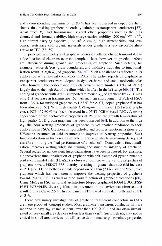
In thin metal films, the surface scattering of free charge carriers causes aninverse relationship between film resistivity and thickness. As a result, there is athreshold below which further reduction in thickness leads to dramatic increases inRsh of the metal film. This critical threshold thickness is observed to lie between 5and 10 nm in commonly employed electrode metals such as Al, Au, and Ag aspredicted by Fuchs-Sondheimer (FS)-Mayadas-Shatzes (MS) model and alsoexperimentally observed [74, 75]. The FS-MS model accounts for surface scat-tering as well as scattering from the grain boundaries. At a thickness of 10 nm, atransmission of the Ag film is observed to be *60 % (Fig. 15) [74, 75]. Metalsalso exhibit very high reflection. Calculations have shown that while absorption of10 nm thick silver is merely 3 %, reflections can amount to 63 % [76]. A dielectriccapping layer, similar to antireflection coating, can suppress this reflection andinduce a desired interference pattern enhancing the amount of photons reachingthe photoactive layer in a solar cell. Such a capping layer can be either organic orinorganic dielectric compounds materials [77]. Coating of a metal electrode withaluminum hydroxiquinoline (Alq3) in small molecular-based solar cell is reportedto cause an improvement in photocurrent up to 50 % [77, 78].
A very few scientific reports are available on thin metal films as transparentconductor in the fabrication of PSCs [74, 79, 80]. Nonetheless, ultrathin metallayer has been adopted as transparent conductors in PSCs in both top-and bottom-illuminated inverted architectures. In bottom illuminated solar cell with thestructure substrate/ultrathin Au /ZnO/P3HT:PCBM/PEDOT:PSS/100 nm Au, aPCE of 2.52 % is observed. Such a PCE is nonetheless lower than the ITO-basedreference devices (PCE: 3.53 %). The lower PCE is mainly attributed to the lowerJsc which in turn is caused by the reduced incoupling of light into the device. In thesame structure when top illuminated realized by using 10 nm thick Au top elec-trode and 100 nm Au bottom electrode, the lowest PCE 1.75 % is observed andwas attributed due to optical transmission loss due to the presence of PEDOT:PSSlayer [79]. The top illuminated inverted structure has been explored in otherstudies and has resulted in poor performance in comparison to that of reference
Indium Tin Oxide-Free Polymer Solar Cells 211
devices. In such a structure, controlling the metal film properties on differentsubstrates is not an easy task. Film morphology is affected by the type of substrateand its roughness, the surface treatment of the substrate, and the deposition con-ditions [75]. Without any morphological control, it is unlikely that small amountsof Au or Ag can be deposited on PEDOT:PSS can result in continuous films.Several authors have noticed that Ag has a tendency to coalesce when deposited onorganic layers. Incorporating processing strategies to achieve continuous filmformation of Ag or Au on organic layer may reduce the loss in performance. Suchstrategies involve deposition of a work function compatible low-surface energymetals. For example, MgAg can form very flat semitransparent metal filmsat \5 nm thickness while Ag forms island [81, 82].
Ultrathin metal films have been deposited by evaporation. However, recently asolution processed semitransparent Ag electrode was reported having a Rsh of 5 X!-1 and a corresponding transmission of 30 % at 550 nm along with a roughnessof 2 nm. When incorporated in the fabrication of a P3HT: PCBM-based solar cell,a PCE: 1.6 %; FF: * 60 %; Voc: 0.51 V; and Jsc:5.3 mA/cm2 was observed. Thelow Jsc is attributed to lower incoupling of light [83].
3.4 Polymers
The most important advantage of polymeric transparent conductors is that they canbe solution processed and are therefore readily processed in an R2R setup usingthe plethora of coating and printing techniques available [39]. Poly(3,4-ethyl-enedioxythiophene):poly(styrenesulfonate) or PEDOT:PSS is the most widely
Fig. 15 Thickness dependence of sheet resistance in ultra-thin gold films determined bysimulation based on FS-MS model (solid line) and experimentally verified (dots). Inset showsvisible transmission of ultra-thin Au films with various thicknesses. The dashed line isabsorbance of P3HT:PCBM. � 2013 Elsevier. Reprinted, with permission from Ref. [74]
212 D. Angmo et al.
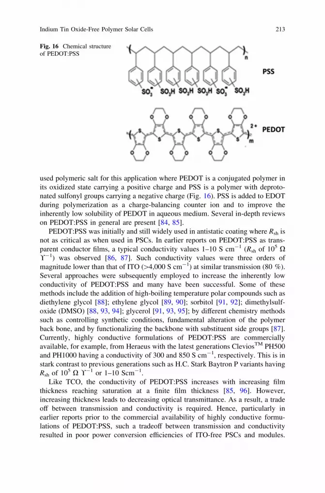
used polymeric salt for this application where PEDOT is a conjugated polymer inits oxidized state carrying a positive charge and PSS is a polymer with deproto-nated sulfonyl groups carrying a negative charge (Fig. 16). PSS is added to EDOTduring polymerization as a charge-balancing counter ion and to improve theinherently low solubility of PEDOT in aqueous medium. Several in-depth reviewson PEDOT:PSS in general are present [84, 85].
PEDOT:PSS was initially and still widely used in antistatic coating where Rsh isnot as critical as when used in PSCs. In earlier reports on PEDOT:PSS as trans-parent conductor films, a typical conductivity values 1–10 S cm-1 (Rsh of 105 X!-1) was observed [86, 87]. Such conductivity values were three orders ofmagnitude lower than that of ITO ([4,000 S cm-1) at similar transmission (80 %).Several approaches were subsequently employed to increase the inherently lowconductivity of PEDOT:PSS and many have been successful. Some of thesemethods include the addition of high-boiling temperature polar compounds such asdiethylene glycol [88]; ethylene glycol [89, 90]; sorbitol [91, 92]; dimethylsulf-oxide (DMSO) [88, 93, 94]; glycerol [91, 93, 95]; by different chemistry methodssuch as controlling synthetic conditions, fundamental alteration of the polymerback bone, and by functionalizing the backbone with substituent side groups [87].Currently, highly conductive formulations of PEDOT:PSS are commerciallyavailable, for example, from Heraeus with the latest generations CleviosTM PH500and PH1000 having a conductivity of 300 and 850 S cm-1, respectively. This is instark contrast to previous generations such as H.C. Stark Baytron P variants havingRsh of 105 X !-1 or 1–10 Scm-1.
Like TCO, the conductivity of PEDOT:PSS increases with increasing filmthickness reaching saturation at a finite film thickness [85, 96]. However,increasing thickness leads to decreasing optical transmittance. As a result, a tradeoff between transmission and conductivity is required. Hence, particularly inearlier reports prior to the commercial availability of highly conductive formu-lations of PEDOT:PSS, such a tradeoff between transmission and conductivityresulted in poor power conversion efficiencies of ITO-free PSCs and modules.
Fig. 16 Chemical structureof PEDOT:PSS
Indium Tin Oxide-Free Polymer Solar Cells 213
In some cases, PEDOT:PSS having transmission in the range 10–30 %(350–600 nm) for a comparable Rsh to ITO (10–20 X !-1) has been reported [97].As a result, often PSC devices-based PEDOT: PSS delivered lower PCE than ITO-based reference devices [89, 91, 98]. Subsequently, the use of highly conductive(hc) PEDOT:PSS such as PH500 as transparent conductor has resulted in com-parable performance to ITO-based control devices. A maximum PCE of 3.27 %,Voc: 0.63 V, Jsc: 9.7 mA cm-2, FF: 53.5 % have been reported [99].
In the inverted device configuration, a PCE of 3.08 %, Voc: 0.61 V; Jsc:9.1 mA cm-2; FF: 53.3 % is reported in solar cells based on hcPEDOT:PSStransparent conductor and evaporated Ag counter electrode. Such a PCE, none-theless, is lower than ITO reference devices having an average PCE: 4.20 %,Jsc: 10.25 mA/cm2, FF: 66.6 %, and Voc: 0.62 V. In such a device, the evaporatedAg counter electrode, can also be replaced with PEDOT:PSS, therefore allowingthe fabrication of an all-solution-processed device [100]. Initially, such a deviceshowed poor rectification with a performance of PCE: 0.47 %, Voc: 0.31 V, Jsc:5.94 mA cm-2, and FF: 27.7 % [100]. However, later reports observed goodrectification with improved ZnO buffer films deposited by atomic layer deposition[101]. With a new generation low-band gap polymer, a PCE of 2.69 % wasobserved in a polymer-based solar cell processed with a roll-coated hcPEDOT:PSSas the front electrode in combination with PEDOT:PSS/Ag as the back electrode[102]. Nonetheless, all such devices had lower PCE than ITO-based referencedevices. However, PEDOT:PSS electrodes render improve mechanical flexibilitythan ITO electrodes where PCE showed a 92 % retention in PEDOT:PSS-basedPSCs while only 50 % of the initial PCE was retained in ITO-based electrode after300 bend cycle [100].
3.5 Metal grid/PEDOT:PSS Composite Electrode
Despite the development of highly conductive formulations of PEDOT: PSS, itsRsh values (102–103 X !-1) still remains significantly higher than ITO (10–60 X!-1) as a result of which stand-alone PEDOT:PSS front electrodes have yieldedlower PCE than ITO-based control devices. By physically reinforcingPEDOT:PSS with metal grids, conductivity of PEDOT:PSS can be significantlyimproved. Such a composite electrode when used in place of ITO in normalstructure solar cells is observed to cause a threefold decrease in series resistance(Rs) from [ 1 kX in cells with only PEDOT:PSS as electrode to 400 X withcomposite electrodes, ultimately resulting in a threefold increase in Jsc [98]. Thechallenge for using such a composite electrode is in the optimization requiredbetween shadow losses due to the metal grids and the resistive losses due to theresistance of the combined PEDOT:PSS/metal electrode. Depending on the Rsh ofPEDOT:PSS films, completely different configurations of metal grid design arerequired in the optimization of the cells [103]. Overall, the surface coverage of themetal grids should be as small as possible so as to minimize loss of incoming
214 D. Angmo et al.
radiation reaching the photoactive layer. Conductivity can be increasing byincreasing line height while maintaining minimum shading losses [104]. In gen-eral, for a given PEDOT:PSS, the optimized geometry of the metal grid that resultsin minimum shading fractional power losses is simply given by the empiricalrelation (W / W + S) where W is the grid width and S is the grid separation [103,105].
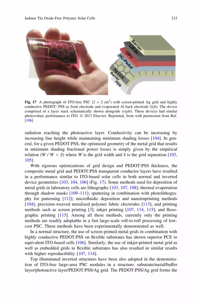
With rigorous optimizations of grid design and PEDOT:PSS thickness, thecomposite metal grid and PEDOT:PSS transparent conductor layers have resultedin a performance similar to ITO-based solar cells in both normal and inverteddevice geometries [103, 104, 106] (Fig. 17). Some methods used for deposition ofmetal grids in laboratory cells are lithography [103, 107, 108]; thermal evaporationthrough shadow masks [109–111]; sputtering in combination with photolithogra-phy for patterning [112]; microfluidic deposition and nanoimprinting methods[104]; precision-weaved metalized polymer fabric electrodes [113]; and printingmethods such as screen printing [3]; inkjet printing [107, 114, 115]; and flexo-graphic printing [115]. Among all these methods, currently only the printingmethods are readily adoptable in a fast large-scale roll-to-roll processing of low-cost PSC. These methods have been experimentally demonstrated as well.
In a normal structure, the use of screen-printed metal grids in combination withhighly conductive PEDOT:PSS on flexible substrates has shown superior PCE toequivalent ITO-based cells [106]. Similarly, the use of inkjet-printed metal grid aswell as embedded grids in flexible substrates has also resulted in similar resultswith higher reproducibility [107, 114].
Top illuminated inverted structures have been also adopted in the demonstra-tion of ITO-free large-area PSC modules in a structure: substrate/metal/bufferlayer/photoactive layer/PEDOT:PSS/Ag grid. The PEDOT:PSS/Ag grid forms the
Fig. 17 A photograph of ITO-free PSC (2 9 2 cm2) with screen-printed Ag grid and highlyconductive PEDOT: PSS as front electrode and evaporated Al back electrode (left). The devicecomprised of a layer stack schematically shown alongside (right). These devices had similarphotovoltaic performance to ITO. � 2013 Elsevier. Reprinted, from with permission from Ref.[106]
Indium Tin Oxide-Free Polymer Solar Cells 215
front electrode and the metal layer on the substrate forms as the back electrode. Arange of metals has been applied as back electrodes, for example, Ag, Al/Cr, andCu/Ti [116–118]. The choice of metal for back electrodes can allow tuning of thework function of the electrode allowing higher voltage extraction and thereforehigher PCE. This is observed in small devices when Ag grid is deposited byevaporation which in turn allows PEDOT:PSS layer to be made very thin, ulti-mately allowing superior light transmission into the device. When Ag grid isdeposited by ambient processing technique such as screen printing, a higherthickness of PEDOT:PSS because the solvents from screen printing formulation ofAg ink is observed to diffuse through the underlying PEDOT:PSS layer into thephotoactive layer, thereby destroying it. Consequently, the higher thickness ofPEDOT:PSS leads to poor transmission to the PAL and thereby very poor current.In early reports on R2R produced screen-printed grids, a transmission as low as30 % is reported [116–118].
The most recent advancement in ITO-free R2R produced modules were madein bottom illuminated inverted structures. A vacuum-free all R2R-processed PSCsemploying high conductive PEDOT:PSS/metal grid as a front electrode andPEDOT:PSS/metal grid as the back electrode in an inverted structure was recentlydemonstrated [115]. Metal grids were printed by three R2R methods: R2R thermalimprinting of embedded grids, R2R inkjet printing, and R2R flexographic printing.R2R flexographic-printed and R2R-embedded grids delivered similar albeitunprecedented performance for fully R2R processed vacuum-free large-area ITO-free cells (active area 6 cm2) under ambient conditions with devices based on flexogrids having a PCE: 1.82 %, Jsc: 7.1 mA cm-2, Voc:5.1 V, FF: 51.2 %, andembedded grids with PCE: 1.92 %, Jsc: 7.06 mA cm-2, Voc: 0.50 V, FF: 54.6 %.The raised topography and relatively poor conductivities in the R2R inkjet-printedsilver grids resulted in significantly lower PCE attributed to the lower FF and Jsc
caused as a result of shunt paths: PCE 0.75 %, Jsc: 4.27 mA cm-2, Voc: 0.50 V,and FF: 35.1 %. Among all these techniques, flexographic printing emerged to bethe favorable low-cost technique presenting no topography issues and the need formultiple R2R steps as required in the embedded grids. Flexographic printing hasbeen recently adopted in producing large-area modules that are produced by allR2R processing and have delivered PCE comparable to ITO-based devices. This isdiscussed in the next section.
4 Roll-to-Roll Processing of ITO-Free Polymer Solar CellModules
To date, almost all polymer solar cells reported in the literature are prepared usinga combination of two laboratory techniques: spin coating and metal evaporation.However, neither of these techniques can be expected to share a future with PSCs,where only processes that rely on flexible substrates and the absence of vacuumsteps are expected.
216 D. Angmo et al.
Solution-based processing is an appealing alternative to vacuum-based depo-sition approaches. The straightforward comparative advantages of solution meth-ods include atmospheric pressure processing, which requires significantly lowercapital equipment costs, suitability for large-area and flexible substrates, higherthroughput, and the combination of more efficient materials usage and lowertemperature processing. These approaches can also be readily adapted for simul-taneously patterning the materials while coating or printing, which eliminates theneed for additional processing steps.
An enormous palette of film-forming techniques has been investigated forprocessing one or more of the layers in a PSC, which usually is comprised of fiveor six layers. Some of these film-forming techniques investigated are slot diecoating, gravure coating, knife-over-edge coating, offset coating, spray coating,and printing techniques such as inkjet printing, pad printing, and screen printing.A complete review on roll-to-roll processing can be found elsewhere [39, 119].
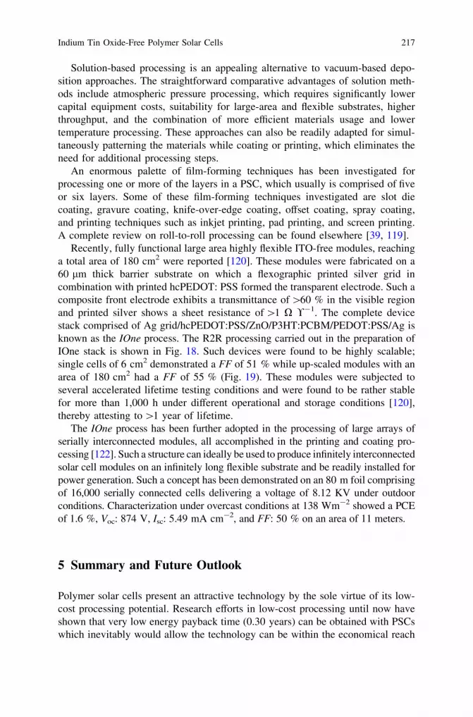
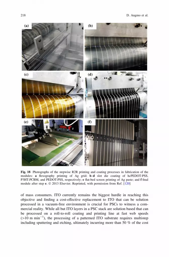
Recently, fully functional large area highly flexible ITO-free modules, reachinga total area of 180 cm2 were reported [120]. These modules were fabricated on a60 lm thick barrier substrate on which a flexographic printed silver grid incombination with printed hcPEDOT: PSS formed the transparent electrode. Such acomposite front electrode exhibits a transmittance of [60 % in the visible regionand printed silver shows a sheet resistance of [1 X !-1. The complete devicestack comprised of Ag grid/hcPEDOT:PSS/ZnO/P3HT:PCBM/PEDOT:PSS/Ag isknown as the IOne process. The R2R processing carried out in the preparation ofIOne stack is shown in Fig. 18. Such devices were found to be highly scalable;single cells of 6 cm2 demonstrated a FF of 51 % while up-scaled modules with anarea of 180 cm2 had a FF of 55 % (Fig. 19). These modules were subjected toseveral accelerated lifetime testing conditions and were found to be rather stablefor more than 1,000 h under different operational and storage conditions [120],thereby attesting to [1 year of lifetime.
The IOne process has been further adopted in the processing of large arrays ofserially interconnected modules, all accomplished in the printing and coating pro-cessing [122]. Such a structure can ideally be used to produce infinitely interconnectedsolar cell modules on an infinitely long flexible substrate and be readily installed forpower generation. Such a concept has been demonstrated on an 80 m foil comprisingof 16,000 serially connected cells delivering a voltage of 8.12 KV under outdoorconditions. Characterization under overcast conditions at 138 Wm-2 showed a PCEof 1.6 %, Voc: 874 V, Isc: 5.49 mA cm-2, and FF: 50 % on an area of 11 meters.
5 Summary and Future Outlook
Polymer solar cells present an attractive technology by the sole virtue of its low-cost processing potential. Research efforts in low-cost processing until now haveshown that very low energy payback time (0.30 years) can be obtained with PSCswhich inevitably would allow the technology can be within the economical reach
Indium Tin Oxide-Free Polymer Solar Cells 217
of mass consumers. ITO currently remains the biggest hurdle in reaching thisobjective and finding a cost-effective replacement to ITO that can be solutionprocessed in a vacuum-free environment is crucial for PSCs to witness a com-mercial reality. While all but ITO layers in a PSC stack are solution based that canbe processed on a roll-to-roll coating and printing line at fast web speeds([10 m min-1), the processing of a patterned ITO substrate requires multistepincluding sputtering and etching, ultimately incurring more than 50 % of the cost
Fig. 18 Photographs of the stepwise R2R printing and coating processes in fabrication of themodules: a flexography printing of Ag grid; b–d slot die coating of hcPEDOT:PSS,P3HT:PCBM, and PEDOT:PSS, respectively; e flat-bed screen printing of Ag paste; and f finalmodule after step e. � 2013 Elsevier. Reprinted, with permission from Ref. [120]
218 D. Angmo et al.
of a PSC module. Hence, finding an alternative is crucial for the successfulcommercialization of PSCs.
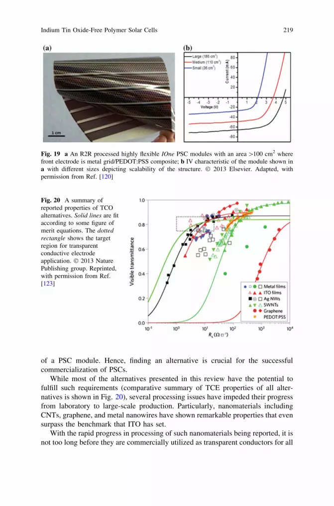
While most of the alternatives presented in this review have the potential tofulfill such requirements (comparative summary of TCE properties of all alter-natives is shown in Fig. 20), several processing issues have impeded their progressfrom laboratory to large-scale production. Particularly, nanomaterials includingCNTs, graphene, and metal nanowires have shown remarkable properties that evensurpass the benchmark that ITO has set.
With the rapid progress in processing of such nanomaterials being reported, it isnot too long before they are commercially utilized as transparent conductors for all
Fig. 20 A summary ofreported properties of TCOalternatives. Solid lines are fitaccording to some figure ofmerit equations. The dottedrectangle shows the targetregion for transparentconductive electrodeapplication. � 2013 NaturePublishing group. Reprinted,with permission from Ref.[123]
Fig. 19 a An R2R processed highly flexible IOne PSC modules with an area [100 cm2 wherefront electrode is metal grid/PEDOT:PSS composite; b IV characteristic of the module shown ina with different sizes depicting scalability of the structure. � 2013 Elsevier. Adapted, withpermission from Ref. [120]
Indium Tin Oxide-Free Polymer Solar Cells 219
optoelectronics in general and organic solar cells in particular. Meanwhile, thecomposite PEDOT:PSS/metal grid electrode remains the readily available andupscalable alternative to ITO.
References
1. Espinosa N, García-Valverde R, Urbina A, Krebs FC (2011) A life cycle analysis ofpolymer solar cell modules prepared using roll-to-roll methods under ambient conditions.Sol Energy Mater Sol Cells 95(5):1293–1302
2. Espinosa N, Hösel M, Angmo D, Krebs FC (2012) Solar cells with one-day energy paybackfor the factories of the future. Energy Environ Sci 1:5117
3. Krebs FC, Tromholt T, Jørgensen M (2010) Upscaling of polymer solar cell fabricationusing full roll-to-roll processing. Nanoscale 2(6):873–886
4. Krebs FC, Gevorgyan SA, Alstrup J (2009) A roll-to-roll process to flexible polymer solarcells: model studies, manufacture and operational stability studies. J Mater Chem19(30):5442–5451
5. Emmott CJM, Urbina A, Nelson J (2012) Environmental and economic assessment of ITO-free electrodes for organic solar cells. Sol Energy Mater Sol Cells 97:14–21
6. Azzopardi B, Emmott CJM, Urbina A, Krebs FC, Mutale J, Nelson J (2011) Economicassessment of solar electricity production from organic-based photovoltaic modules in adomestic environment. Energy Environ Sci 4:3741
7. Nelson J (2011) Polymer: fullerene bulk heterojunction solar cells. Mater Today 201114(10):462–470
8. Helgesen M, Søndergaard R, Krebs FC (2010) Advanced materials and processes forpolymer solar cell devices. J Mater Chem 20(1):36
9. Brabec CJ, Gowrisanker S, Halls JJM, Laird D, Jia S, Williams SP (2010) Polymer:fullerene bulk-heterojunction solar cells. Adv Mater 22(34):3839–3856
10. Deibel C, Dyakonov V (2010) Polymer-fullerene bulk heterojunction solar cells. Rep ProgPhys 73(9):096401
11. XXX12. Rowell MW, McGehee MD (2011) Transparent electrode requirements for thin film solar
cell modules. Energy Environ Sci 4(1):13113. Gordon R (2000) Criteria for choosing transparent conductors. MRS Bull 25(8):52–5714. Kang M, Park HJ, Ahn SH, Xu T, Guo LJ (2010) Toward low-cost, high-efficiency, and
scalable organic solar cells with transparent metal electrode and improved domainmorphology. IEEE J Sel Top Quantum Electron 16(6):1807–1820
15. Liu C, Kamaev V, Vardeny ZV (2005) Efficiency enhancement of an organic light-emittingdiode with a cathode forming two-dimensional periodic hole array. Appl Phys Lett86(14):143501
16. van de Groep J, Spinelli P, Polman A (2012) Transparent conducting silver nanowirenetworks. Nano Lett 12(6):3138
17. Catrysse PB, Fan S (2010) Nanopatterned metallic films for use as transparent conductiveelectrodes in optoelectronic devices. Nano Lett 10(8):2944
18. Kang M, Kim M, Kim J, Guo LJ (2008) Organic solar cells using nanoimprinted transparentmetal electrodes. Adv Mater 20(23):4624
19. Kang M, Joon Park H, Hyun Ahn S, Jay Guo L (2010) Transparent Cu nanowire meshelectrode on flexible substrates fabricated by transfer printing and its application in organicsolar cells. Sol Energy Mater Sol Cells 94(6):1179–1184
20. Kang M, Park HJ, Ahn SH, Xu T, Guo LJ (2010) Toward low-cost, high-efficiency, andscalable organic solar cells with transparent metal electrode and improved domainmorphology. IEEE J Sel Top Quantum Electron 16(6):1807
220 D. Angmo et al.
21. Byeon K, Lee H (2012) Recent progress in direct patterning technologies based on nano-imprint lithography. Eur Phys J Appl Phys 59(1):10001
22. Kang M, Guo LJ (2007) Semitransparent Cu electrode on a flexible substrate and itsapplication in organic light emitting diodes. J Vac Sci Technol, B 25(6):2637
23. Guo LJ (2007) Nanoimprint lithography: methods and material requirements. Adv Mater19(4):495
25. Ahn SH, Guo LJ (2008) High-speed roll-to-roll nanoimprint lithography on flexible plasticsubstrates. Adv Mater 20(11):2044
26. Kang M, Guo LJ (2007) Nanoimprinted semitransparent metal electrodes and theirapplication in organic light-emitting diodes. Adv Mater 19(10):1391
27. Lee J, Connor ST, Cui Y, Peumans P (2008) Solution-processed metal nanowire meshtransparent electrodes. Nano Lett 8(2):689
28. Hu L, Wu H, Cui Y (2011) Metal nanogrids, nanowires, and nanofibers for transparentelectrodes. MRS Bull 36(10):760
29. Wu H, Hu L, Rowell MW, Kong D, Cha JJ, McDonough JR et al (2010) Electrospun metalnanofiber webs as high-performance transparent electrode. Nano Lett 10(10):4242
30. Gaynor W, Lee J, Peumans P (2010) Fully solution-processed inverted polymer solar cellswith laminated nanowire electrodes. ACS Nano 4(1):30–34
31. Yang L, Zhang T, Zhou H, Price SC, Wiley BJ, You W (2011) Solution-processed flexiblepolymer solar cells with silver nanowire electrodes. Acs Appl Mater Interfaces 3(10):4075
32. Leem D, Edwards A, Faist M, Nelson J, Bradley DDC, de Mello JC (2011) Efficient organicsolar cells with solution-processed silver nanowire electrodes. Adv Mater 23(38):4371
33. Zhu R, Chung C, Cha KC, Yang W, Zheng YB, Zhou H et al (2011) Fused silver nanowireswith metal oxide nanoparticles and organic polymers for highly transparent conductors.ACS Nano 5(12):9877–9882
34. De S, Higgins TM, Lyons PE, Doherty EM, Nirmalraj PN, Blau WJ et al (2009) Silvernanowire networks as flexible, transparent, conducting films: extremely high DC to opticalconductivity ratios. ACS Nano 3(7):1767
35. Madaria AR, Kumar A, Zhou C (2011) Large scale, highly conductive and patternedtransparent films of silver nanowires on arbitrary substrates and their application in touchscreens. Nanotechnology 22(24):245201
36. Scardaci V, Coull R, Rickard D, Coleman JN (2011) Spray deposition of highly transparent,low resistance networks of silver nanowires over large areas. Small 7(8):2621–2628
37. Choi DY, Kang HW, Sung HJ, Kim SS (2013) Annealing-free, flexible silver nanowire-polymer composite electrodes via a continuous two-step spray-coating method. Nanoscale5:977–983
38. Hu L, Kim HS, Lee J, Peumans P, Cui Y (2010) Scalable coating and properties oftransparent, flexible, silver nanowire electrodes. ACS Nano 4(5):2955
39. Søndergaard R, Hösel M, Angmo D, Larsen-Olsen TT, Krebs FC (2012) Roll-to-rollfabrication of polymer solar cells. Mater Today 15(1–2):36–49
40. Spechler JA, Arnold CB (2012) Direct-write pulsed laser processed silver nanowirenetworks for transparent conducting electrodes. Appl Phys A-Mater Sci Process 108(1):25
41. Jiu J, Nogi M, Sugahara T, Tokuno T, Araki T, Komoda N et al (2012) Strongly adhesiveand flexible transparent silver nanowire conductive films fabricated with a high-intensitypulsed light technique. J Mater Chem 22(44):23561
42. Hecht DS, Hu L, Irvin G (2011) Emerging transparent electrodes based on thin films ofcarbon nanotubes, graphene, and metallic nanostructures. Adv Mater 23(13):1482
43. Shim BS, Tang Z, Morabito MP, Agarwal A, Hong H, Kotov NA (2007) Integration ofconductivity transparency, and mechanical strength into highly homogeneous layer-by-layercomposites of single-walled carbon nanotubes for optoelectronics. Chem Mater 19(23):5467
Indium Tin Oxide-Free Polymer Solar Cells 221
44. Wu ZC, Chen ZH, Du X, Logan JM, Sippel J, Nikolou M et al (2004) Transparent,conductive carbon nanotube films. Science 305(5688):1273
46. Tenent RC, Barnes TM, Bergeson JD, Ferguson AJ, To B, Gedvilas LM et al (2009)Ultrasmooth, large-area, high-uniformity, conductive transparent single-walled-carbon-nanotube films for photovoltaics produced by ultrasonic spraying. Adv Mater 21(31):3210
47. Barnes TM, Bergeson JD, Tenent RC, Larsen BA, Teeter G, Jones KM et al (2010) Carbonnanotube network electrodes enabling efficient organic solar cells without a hole transportlayer. Appl Phys Lett 96(24):243309
48. Pasquier AD, Unalan HE, Kanwal A, Miller S, Chhowalla M (2005) Conducting andtransparent single-wall carbon nanotube electrodes for polymer-fullerene solar cells. ApplPhys Lett 87(20):1–3
49. van de Lagemaat J, Barnes TM, Rumbles G, Shaheen SE, Coutts TJ, Weeks C et al (2006)Organic solar cells with carbon nanotubes replacing In2O3: Sn as the transparent electrode.Appl Phys Lett 88(23):233503
50. Rowell MW, Topinka MA, McGehee MD, Prall H, Dennler G, Sariciftci NS et al (2006)Organic solar cells with carbon nanotube network electrodes. Appl Phys Lett 88(23):233506
51. Li Z, Kandel HR, Dervishi E, Saini V, Xu Y, Biris AR et al (2008) Comparative study ondifferent carbon nanotube materials in terms of transparent conductive coatings. Langmuir24(6):2655–2662
52. Kim S, Yim J, Wang X, Bradley DDC, Lee S, de Mello JC (2010) Spin- and spray-depositedsingle-walled carbon-nanotube electrodes for organic solar cells. Adv Funct Mater20(14):2310–2316
53. Kim S, Wang X, Yim JH, Tsoi WC, Kim J, Lee S et al (2012) Efficient organic solar cellsbased on spray-patterned single wall carbon nanotube electrodes. J Photonics Eng2(1):021010–021011
54. Geim AK, Novoselov KS (2007) The rise of graphene. Nat Mater 6(3):18355. Bonaccorso F, Sun Z, Hasan T, Ferrari AC (2010) Graphene photonics and optoelectronics.
Nat Photonics 4(9):611–62256. Lv R, Terrones M (2012) Towards new graphene materials: doped graphene sheets and
nanoribbons. Mater Lett 78:209–21857. Bae S, Kim H, Lee Y, Xu X, Park J, Zheng Y et al (2010) Roll-to-roll production of 30-inch
graphene films for transparent electrodes. Nat Nanotechnol 5(8):574–57858. Kang J, Hwang S, Kim JH, Kim MH, Ryu J, Seo SJ et al (2012) Efficient transfer of large-
area graphene films onto rigid substrates by hot pressing. ACS Nano 6(6):536059. Park H, Brown PR, Buloyic V, Kong J (2012) Graphene as transparent conducting
electrodes in organic photovoltaics: studies in graphene morphology, hole transportinglayers, and counter electrodes. Nano Lett 12(1):133
60. Wu J, Becerril HA, Bao Z, Liu Z, Chen Y, Peumans P (2008) Organic solar cells withsolution-processed graphene transparent electrodes. Appl Phys Lett 92(26):263302
61. Wang X, Zhi L, Muellen K (2008) Transparent, conductive graphene electrodes for dye-sensitized solar cells. Nano Lett 8(1):323
62. Kim KK, Reina A, Shi Y, Park H, Li L, Lee YH et al (2010) Enhancing the conductivity oftransparent graphene films via doping. Nanotechnology 21(28):285205
63. Park H, Rowehl JA, Kim KK, Bulovic V, Kong J (2010) Doped graphene electrodes fororganic solar cells. Nanotechnology 21(50):505204
64. Choe M, Lee BH, Jo G, Park J, Park W, Lee S et al (2010) Efficient bulk-heterojunctionphotovoltaic cells with transparent multi-layer graphene electrodes. Org Electron11(11):1864
65. Wang Y, Chen X, Zhong Y, Zhu F, Loh KP (2009) Large area, continuous, few-layeredgraphene as anodes in organic photovoltaic devices. Appl Phys Lett 95(6):063302
222 D. Angmo et al.
66. Wang Y, Tong SW, Xu XF, Oezyilmaz B, Loh KP (2011) Interface engineering of layer-by-layer stacked graphene anodes for high-performance organic solar cells. Adv Mater23(13):1514–1518
67. Kim KS, Zhao Y, Jang H, Lee SY, Kim JM, Kim KS et al (2009) Large-scale pattern growthof graphene films for stretchable transparent electrodes. Nature 457(7230):706
68. Pang S, Hernandez Y, Feng X, Muellen K (2011) Graphene as transparent electrodematerial for organic electronics. Adv Mater 23(25):2779
69. Huang X, Yin Z, Wu S, Qi X, He Q, Zhang Q et al (2011) Graphene-based materials:synthesis, characterization, properties, and applications. Small 7(14):1876
70. Jo G, Choe M, Lee S, Park W, Kahng YH, Lee T (2012) The application of graphene aselectrodes in electrical and optical devices. Nanotechnology 23(11):112001
71. Castañeda L (2011) Present status of the development and application of transparentconductors oxide thin solid films. Mater Sci Appl 2:1233
72. Zhou H, Yi D, Yu Z, Xiao L, Li J (2007) Preparation of aluminum doped zinc oxide filmsand the study of their microstructure, electrical and optical properties. Thin Solid Films515(17):6909–6914
73. Kumar A, Zhou C (2010) The race to replace tin-doped indium oxide: which material willwin? ACS Nano 4(1):11
74. Wilken S, Hoffmann T, von Hauff E, Borchert H, Parisi J (2012) ITO-free inverted polymer/fullerene solar cells: Interface effects and comparison of different semi-transparent frontcontacts. Sol Energy Mater Sol Cells 96(1):141–147
75. O’Connor B, Haughn C, An K, Pipe KP, Shtein M (2008) Transparent and conductiveelectrodes based on unpatterned, thin metal films. Appl Phys Lett 93(22):223304
76. Koeppe R, Hoeglinger D, Troshin PA, Lyubovskaya RN, Razumov VF, Sariciftci NS (2009)Organic solar cells with semitransparent metal back contacts for power windowapplications. Chemsuschem 2(4):309
77. O’Connor B, An KH, Pipe KP, Zhao Y, Shtein M (2006) Enhanced optical field intensitydistribution in organic photovoltaic devices using external coatings. Appl Phys Lett89(23):233502
78. Meiss J, Furno M, Pfuetzner S, Leo K, Riede M (2010) Selective absorption enhancement inorganic solar cells using light incoupling layers. J Appl Phys 107(5):053117
79. Ajuria J, Etxebarria I, Cambarau W, Munecas U, Tena-Zaera R, Carlos Jimeno J et al (2011)Inverted ITO-free organic solar cells based on p and n semiconducting oxides. New designsfor integration in tandem cells, top or bottom detecting devices, and photovoltaic windows.Energy Environ Sci 4(2):453–458
80. Al-Ibrahim M, Sensfuss S, Uziel J, Ecke G, Ambacher O (2005) Comparison of normal andinverse poly(3-hexylthiophene)/fullerene solar cell architectures. Sol Energy Mater SolCells 85(2):277–283
81. Meiss J, Riede MK, Leo K (2009) Optimizing the morphology of metal multilayer films forindium tin oxide (ITO)-free inverted organic solar cells. J Appl Phys 105(6):063108
82. Oyamada T, Sugawara Y, Terao Y, Sasabe H, Adachi C (2007) Top light-harvesting organicsolar cell using ultrathin Ag/MgAg layer as anode. Japan J Appl Phys Part 1-Regular PapersBrief Communications & Review Papers 2007;46(4A):1734
83. Angmo D, Hösel M, Krebs FC (2012) All solution processing of ITO-free organic solar cellmodules directly on barrier foil. Sol Energy Mater Sol Cells 107:329–336
84. Kirchmeyer S, Reuter K (2005) Scientific importance, properties and growing applicationsof poly(3,4-ethylenedioxythiophene). J Mater Chem 15(21):2077
85. Levermore PA, Chen L, Wang X, Das R, Bradley DDC (2007) Highly conductive poly(3,4-ethylenedioxythiophene) films by vapor phase polymerization for application in efficientorganic light-emitting diodes. Adv Mater 19(17):2379
86. Groenendaal BL, Jonas F, Freitag D, Pielartzik H, Reynolds JR (2000) Poly(3,4-ethylenedioxythiophene) and its derivatives: past, present, and future. Adv Mater 12(7):481
Indium Tin Oxide-Free Polymer Solar Cells 223
87. Ha YH, Nikolov N, Pollack SK, Mastrangelo J, Martin BD, Shashidhar R (2004) Towards atransparent, highly conductive poly(3,4-ethylenedioxythiophene). Adv Funct Mater14(6):615
88. Hsiao Y, Whang W, Chen C, Chen Y (2008) High-conductivity poly(3,4-ethylenedioxythiophene): poly(styrene sulfonate) film for use in ITO-free polymer solarcells. J Mater Chem 18(48):5948–5955
89. Ouyang BY, Chi CW, Chen FC, Xi QF, Yang Y (2005) High-conductivity poly (3,4-ethylenedioxythiophene): poly(styrene sulfonate) film and its application in polymeroptoelectronic devices. Adv Funct Mater 15(2):203
90. Chang Y, Wang L, Su W (2008) Polymer solar cells with poly(3,4-ethylenedioxythiophene)as transparent anode. Org Electron 9(6):968
91. Zhang FL, Johansson M, Andersson MR, Hummelen JC, Inganas O (2002) Polymerphotovoltaic cells with conducting polymer anodes. Adv Mater 14(9):662
92. Admassie S, Zhang FL, Manoj AG, Svensson M, Andersson MR, Ingaas O (2006) Apolymer photodiode using vapour-phase polymerized PEDOT as an anode. Sol EnergyMater Sol Cells 90(2):133
93. Ahlswede E, Hanisch J, Powalla M (2007) Comparative study of the influence of LiF, NaF,and KF on the performance of polymer bulk heterojunction solar cells. Appl Phys Lett90(16):163504
94. Do H, Reinhard M, Vogeler H, Puetz A, Klein MFG, Schabel W et al (2009) Polymericanodes from poly(3,4-ethylenedioxythiophene): poly(styrenesulfonate) for 3.5 % efficientorganic solar cells. Thin Solid Films 517(20):5900
95. Huang T, Huang C, Su Y, Chen Y, Fang J, Wen T (2010) Extension of active region incrossbar-type polymer solar photovoltaics induced by highly conductive PEDOT:PSS bufferlayer. J Vac Sci Technol, B 28(4):702
96. Zhang XG, Butler WH (1995) Conductivity of metallic-films and multilayers. Phys Rev B51(15):10085
97. Winther-Jensen B, Krebs FC (2006) High-conductivity large-area semi-transparentelectrodes for polymer photovoltaics by silk screen printing and vapour-phase deposition.Sol Energy Mater Sol Cells 90(2):123
98. Aernouts T, Vanlaeke P, Geens W, Poortmans J, Heremans P, Borghs S et al (2004)Printable anodes for flexible organic solar cell modules. Thin Solid Films 451:22
99. Na S, Kim S, Jo J, Kim D (2008) Efficient and flexible ITO-free organic solar cells usinghighly conductive polymer anodes. Adv Mater 20(21):4061
100. Hau SK, Yip H, Zou J, Jen AK (2009) Indium tin oxide-free semi-transparent invertedpolymer solar cells using conducting polymer as both bottom and top electrodes. OrgElectron 10(7):1401
101. Zhou Y, Cheun H, Choi S, Potscavage WJ Jr, Fuentes-Hernandez C, Kippelen B (2010)Indium tin oxide-free and metal-free semitransparent organic solar cells. Appl Phys Lett97(15):153304
102. Larsen-Olsen TT, Machui F, Lechene B, Berny S, Angmo D, Søndergaard R et al (2012)Round-robin studies as a method for testing and validating high-efficiency ITO-freepolymer solar cells based on roll-to-roll-coated highly conductive and transparent flexiblesubstrates. Adv Energy Mater 2(9):1091–1094
103. Tvingstedt K, Inganas O (2007) Electrode grids for ITO-free organic photovoltaic devices.Adv Mater 19(19):2893
104. Kang M, Kim M, Kim J, Guo LJ (2008) Organic solar cells using nanoimprinted transparentmetal electrodes. Adv Mater 20(23):4408
105. Cheknane A (2011) Optimal design of electrode grids dimensions for ITO-free organicphotovoltaic devices. Prog Photovoltaics 19(2):155–159
106. Galagan Y, Rubingh JJM, Andriessen R, Fan C, Blom PWM, Veenstra SC et al (2011) ITO-free flexible organic solar cells with printed current collecting grids. Sol Energy Mater SolCells 95(5):1339–1343
224 D. Angmo et al.
107. Galagan Y, Zimmermann B, Coenen EWC, Jørgensen M, Tanenbaum DM, Krebs FC et al(2012) Current collecting grids for ITO-free solar cells. Adv Energy Mater 2(1):103–110
108. Zou J, Yip H, Hau SK, Jen AK (2010) Metal grid/conducting polymer hybrid transparentelectrode for inverted polymer solar cells. Appl Phys Lett 96(20):203301
109. Zimmermann B, Glatthaar M, Niggemann M, Riede MK, Hinsch A, Gombert A (2007)ITO-free wrap through organic solar cells: a module concept for cost-efficient reel-to-reelproduction. Sol Energy Mater Sol Cells 91(5):374–378
110. Glatthaar M, Niggemann M, Zimmermann B, Lewer P, Riede M, Hinsch A et al (2005)Organic solar cells using inverted layer sequence. Thin Solid Films 491(1–2):298–300
111. Zimmermann B, Schleiermacher HF, Niggemann M, Wuerfel U (2011) ITO-free flexibleinverted organic solar cell modules with high fill factor prepared by slot die coating. SolEnergy Mater Sol Cells 95(7):1587–1589
112. Choi S, Potscavage WJ Jr, Kippelen B (2010) ITO-free large-area organic solar cells. OptExpress 18(19):A458–A466
113. Kylberg W, de Castro FA, Chabrecek P, Sonderegger U, Chu BT, Nüesch F et al (2011)Woven electrodes for flexible organic photovoltaic cells. Adv Mater 23(8):1015–1019
114. Galagan Y, Coenen EWC, Sabik S, Gorter HH, Barink M, Veenstra SC et al (2012)Evaluation of ink-jet printed current collecting grids and busbars for ITO-free organic solarcells. Sol Energy Mater Sol Cells 104:32–38
115. Yu J, Kim I, Kim J, Jo J, Larsen-Olsen TT, Søndergaard RR et al (2012) Silver frontelectrode grids for ITO-free all printed polymer solar cells with embedded and raisedtopographies, prepared by thermal imprint, flexographic and inkjet roll-to-roll processes.Nanoscale 4:6032
116. Krebs FC (2009) All solution roll-to-roll processed polymer solar cells free from indium-tin-oxide and vacuum coating steps. Org Electron 10(5):761–768
117. Manceau M, Angmo D, Jørgensen M, Krebs FC (2011) ITO-free flexible polymer solarcells: from small model devices to roll-to-roll processed large modules. Org Electron12(4):566–574
118. Krebs FC (2009) Roll-to-roll fabrication of monolithic large-area polymer solar cells freefrom indium-tin-oxide. Sol Energy Mater Sol Cells 93(9):1636–1641
119. Krebs FC (2009) Fabrication and processing of polymer solar cells: a review of printing andcoating techniques. Sol Energy Mater Sol Cells 93(4):394–412
120. Angmo D, Gevorgyan SA, Larsen-Olsen TT, Søndergaard R, Hösel M, Jørgensen M et al(2013) Scalability and stability of very thin, roll-to-roll processed, large-area, indium-tin-oxide free polymer solar cells. Org Electron 14(3):984–994
121. Larsen-Olsen TT, Søndergaard RR, Norrman K, Jørgensen M, Krebs FC (2012) All printedtransparent electrodes through an electrical switching mechanism: a convincing alternativeto indium-tin-oxide, silver and vacuum. Energy Environ Sci 15:36–49
122. Sommer-Larsen P, Jørgensen M, Søndergaard RR, Hösel M, Krebs FC (2013) It is all in thepattern–high-efficiency power extraction from polymer solar cells through high-voltageserial connection. Energy Technol 1(1):15–19
123. Ellmer K (2012) Past achievements and future challenges in the development of opticallytransparent electrodes. Nat Photonics 6(12):808