1 23 Wireless Personal Communications An International Journal ISSN 0929-6212 Wireless Pers Commun DOI 10.1007/s11277-014-1823-y Low Voltage Rf Mems Capacitive Shunt Switches Rajneet Kaur, C. C. Tripathi & Dinesh Kumar
Transcript
1 23
Wireless Personal CommunicationsAn International Journal ISSN 0929-6212 Wireless Pers CommunDOI 10.1007/s11277-014-1823-y
Abstract Micro-electro-mechanical-systems(MEMS) switches have low resistive loss, neg-ligible power consumption, good isolation and high power handling capability compared withsemiconductor switches. Lifetime of capacitive shunt switches strongly depends on the actu-ation voltage so low voltage switches is necessary to enhance its performance as well asto broaden its application area. This paper presents the design and simulation of low volt-age capacitive shunt MEMS switches together with its RF performance for high frequencyapplications. The low voltage switches are realized by lowering the spring constant of thebeam using serpentine spring designs together with large capacitive area so as to achieve thegood RF performance as well. The pull-in voltage is analyzed with commercial CAD finiteelement analysis software CoventorWare. The electromagnetic performance in terms of scat-tering parameters, insertion loss, and isolation are analyzed with software Ansoft HFSS10.The switches achieved insertion loss <0.47 dB in on state from 2 to 40 GHz; it providedbetter than 25 dB isolation in off state with a capacitance ratio of 94–96. The actuation volt-age as low as 1.5 V with actuation area 110 × 100 µm2 along with good RF performanceis reported. The design parameter optimization including selection of appropriate numberof meanders and its width found to be one of the most sensitive factors affecting the springstiffness and actuation voltage.
Keywords Actuation voltage · Capacitive shunt switch · Insertion loss · Isolation
1 Introduction
With the advent of MEMS technology, it became possible to develop the low-power andlow-cost miniaturized RF components for high frequency applications. RF-MEMS switches
R. Kaur (B) · C. C. Tripathi · D. KumarDepartment of Electronics & Communication Engineering, University Institute of Engineeringand Technology, Kurukshetra University, Kurukshetra 136119, Haryana, Indiae-mail: [email protected]
123
Author's personal copy
R. Kaur et al.
find its application in many circuits or devices such as tunable-filters, phase-shifters, switch-ing networks, and antenna-arrays etc. MEMS switches exhibit better performance com-pared to conventional semiconductor devices. MEMS switches have low resistive loss,negligible power consumption, good isolation and high power handling capability com-pared with semiconductor switches. Rapid advancement in the design development andunderstanding of RF MEMS switches has been witnessed in the last decades due to itsexcellent performance at microwave to mm-wave frequencies compared to other typesof switches such as GaAs-based FET, pHEMT or PIN-diode switches [1]. RF MEMSswitches can be classified as series or shunt and capacitive or ohmic contact type. Forseries switches, cantilever type beam structure is used and for shunt switches fixed–fixedtype beam is used to open or short the transmission line upon actuation. Series switchesare suitable for lower gigahertz range whereas shunt switches are designed for 10–100 GHzapplications [1].
In quest of low actuation voltage, these switches can be actuated using different actu-ation mechanisms such as electrostatic, magnetic, thermal or piezoelectric and combina-tion of two or more, however, they are unable to avoid the structural complexities andlow switching speed as well as increased power consumptions [2–5]. Therefore, it isvery much clear that the best choice is to reduce the actuation voltage of the electrosta-tic MEMS switches by sorting out various difficulties such as high actuation voltage, lowpower handling capability, relatively low isolation, high insertion loss, large transition timeand particularly insufficient reliability, particularly at Ka band and still high frequencies[3–5].
Further, the electrostatic actuation is most widely employed due to its near zero powerconsumption, small size and less switching time. In order to decrease the actuation voltageof the RF MEMS shunt switches, many efforts such as decrease the airgap, increase thedielectric constant between the capacitive switch plates, increase area of the electrostaticfield have been reported in the recent past [6,7].
Any variation in most of these parameters causes a loss on the other parameters of theswitch, for example, decrease in the gap or increase the area of the electrostatic field causesincrease in off-capacitance and leading to poor switch isolation. The reports are also availableon the reduction of equivalent spring constant of the system by variation of hinges andmaterials so as to reduce the actuation voltage of the switch without compromising on theswitch performance for RF applications [8]. The reducing in the actuation voltage is alwaysat the cost of RF performance i.e. isolation for metal contact switches and insertion loss forcapacitive switches.
Low-loss microwave microelectromechanical systems (MEMS) shunt switches arereported that utilize highly compliant serpentine spring folded suspensions togetherwith large area capacitive actuators to achieve low actuation voltages while main-taining sufficient off-state isolation [6]. Therefore, this study focuses on the realiza-tion of electrostatic low actuation voltage capacitive shunt MEMS switches by low-ering the spring constant of the beam using serpentine spring designs and optimiza-tion of different design parameters including analysis of scattering parameters at Kaband frequencies. As the structure’s dimensions are very critical, resulting optimumspring constant, careful device simulation and recursive optimization of switch para-meters is performed. The pull-in voltage is analyzed with commercial CAD finite ele-ment analysis software CoventorWare. The electromagnetic performance in terms ofscattering parameters, insertion loss, and isolation are analyzed with software AnsoftHFSS.
123
Author's personal copy
Low Voltage Rf Mems
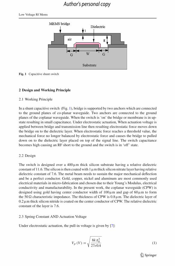
Fig. 1 Capacitive shunt switch
2 Design and Working Principle
2.1 Working Principle
In a shunt capacitive switch (Fig. 1), bridge is supported by two anchors which are connectedto the ground planes of co-planar waveguide. Two anchors are connected to the groundplanes of the coplanar waveguide. When the switch is ‘on’ the bridge or membrane is in up-state resulting in small capacitance. Under electrostatic actuation, When actuation voltage isapplied between bridge and transmission line then resulting electrostatic force moves downthe bridge on to the dielectric layer. When electrostatic force reaches a threshold value, themechanical force no longer balanced by electrostatic force and causes the bridge to pulleddown on to the dielectric layer placed on top of the signal line. The switch capacitancebecomes high causing an RF short to the ground and the switch is in ‘off’ state.
2.2 Design
The switch is designed over a 400µm thick silicon substrate having a relative dielectricconstant of 11.6. The silicon is then coated with 1µm thick silicon nitrate layer having relativedielectric constant of 7.6. The metal beam needs to sustain the major mechanical deflectionand be a perfect conductor. Gold, copper, nickel and aluminum are most commonly usedelectrical materials in micro-fabrication and chosen due to their Young’s Modulus, electricalconductivity and manufacturability. In the present work, the coplanar waveguide (CPW) isdesigned using gold having center conductor width of 100µm and gap of 60µm to formthe 50� characteristic impedance. The thickness of CPW is 0.8µm. The dielectric layer of0.2µm thick silicon nitride is coated on the center conductor of CPW. The relative dielectricconstant of the layer is 7.6.
2.3 Spring Constant AND Actuation Voltage
Under electrostatic actuation, the pull-in voltage is given by [7]:
Vp (V ) =√
8k g30
27ε0A(1)
123
Author's personal copy
R. Kaur et al.
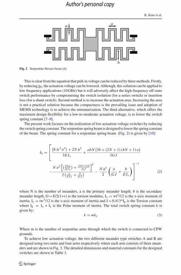
Fig. 2 Serpentine-flexure beam [4]
This is clear from the equation that pull-in voltage can be reduced by three methods. Firstly,by reducing g0, the actuation voltage can be lowered. Although, this solution can be applied tolow frequency applications (10 GHz) but it will adversely affect the high frequency off-stateswitch performance by compromising the switch isolation (for a series switch) or insertionloss (for a shunt switch). Second method is to increase the actuation area. Increasing the areais not a practical solution because the compactness is the prevailing issue and adoption ofMEMS technology is to achieve the miniaturization. The third alternative, which offers themaximum design flexibility for a low-to-moderate actuation voltage, is to lower the switchspring constant [7–9].
The present work focuses on the realization of low actuation voltage switches by reducingthe switch spring constant. The serpentine spring beam is designed to lower the spring constantof the beam. The spring constant for a serpentine spring beam (Fig. 2) is given by [10]:
kz =⎡⎢⎣
(8 N 3 a3
) + 2N b3
3E Ix+ abN [3b + (2N + 1) (4N + 1) a]
3G J
−N a2
[( 2NaE I x
) + (2N+1)bG J
]2
2( a
E I x + bG J
) − N b3
2
(a
G J+ b
E Ix
)⎤⎥⎦
−1
(2)
where N is the number of meanders, a is the primary meander length, b is the secondarymeander length, G = E/2(1+v) is the torsion modulus, Ix = wt3/12 is the x-axis moment ofinertia, Iz = tw3/12 is the z-axis moment of inertia and J = 0.413*Ip is the Torsion constantwhere Ip = Ix + Iz is the Polar moment of inertia. The total switch spring constant k isgiven by:
k = mkz (3)
Where m is the number of serpentine arms through which the switch is connected to CPWgrounds.
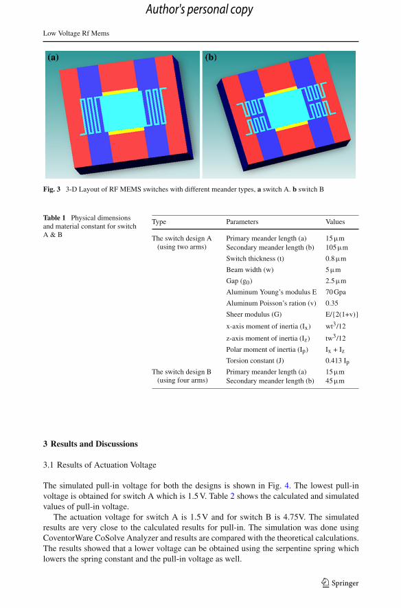
To achieve low actuation voltage, the two different meander type switches A and B aredesigned using two arms and four arms respectively where each arm consists of three mean-ders and are shown in Fig. 3. The detailed dimensions and material constants for the designedswitches are shown in Table 1.
123
Author's personal copy
Low Voltage Rf Mems
Fig. 3 3-D Layout of RF MEMS switches with different meander types, a switch A. b switch B
Table 1 Physical dimensionsand material constant for switchA & B
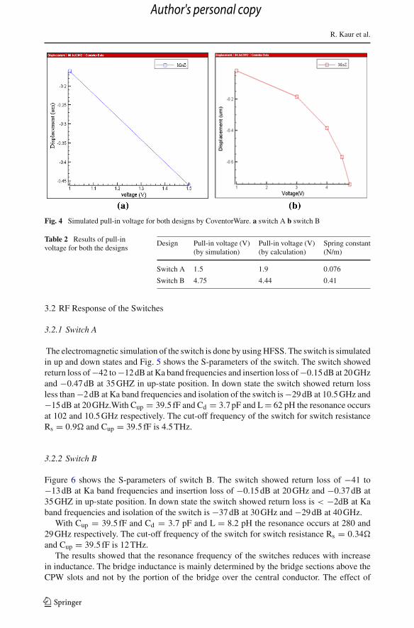
The simulated pull-in voltage for both the designs is shown in Fig. 4. The lowest pull-involtage is obtained for switch A which is 1.5 V. Table 2 shows the calculated and simulatedvalues of pull-in voltage.
The actuation voltage for switch A is 1.5 V and for switch B is 4.75V. The simulatedresults are very close to the calculated results for pull-in. The simulation was done usingCoventorWare CoSolve Analyzer and results are compared with the theoretical calculations.The results showed that a lower voltage can be obtained using the serpentine spring whichlowers the spring constant and the pull-in voltage as well.
123
Author's personal copy
R. Kaur et al.
Fig. 4 Simulated pull-in voltage for both designs by CoventorWare. a switch A b switch B
Table 2 Results of pull-involtage for both the designs
Design Pull-in voltage (V)(by simulation)
Pull-in voltage (V)(by calculation)
Spring constant(N/m)
Switch A 1.5 1.9 0.076
Switch B 4.75 4.44 0.41
3.2 RF Response of the Switches
3.2.1 Switch A
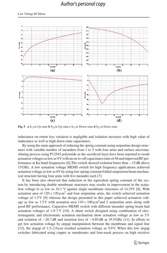
The electromagnetic simulation of the switch is done by using HFSS. The switch is simulatedin up and down states and Fig. 5 shows the S-parameters of the switch. The switch showedreturn loss of −42 to −12 dB at Ka band frequencies and insertion loss of −0.15 dB at 20 GHzand −0.47 dB at 35 GHZ in up-state position. In down state the switch showed return lossless than −2 dB at Ka band frequencies and isolation of the switch is −29 dB at 10.5 GHz and−15 dB at 20 GHz.With Cup = 39.5 fF and Cd = 3.7 pF and L = 62 pH the resonance occursat 102 and 10.5 GHz respectively. The cut-off frequency of the switch for switch resistanceRs = 0.9� and Cup = 39.5 fF is 4.5 THz.
3.2.2 Switch B
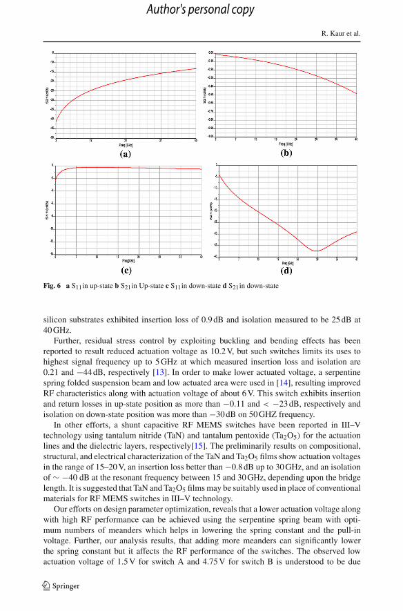
Figure 6 shows the S-parameters of switch B. The switch showed return loss of −41 to−13 dB at Ka band frequencies and insertion loss of −0.15 dB at 20 GHz and −0.37 dB at35 GHZ in up-state position. In down state the switch showed return loss is < −2dB at Kaband frequencies and isolation of the switch is −37 dB at 30 GHz and −29 dB at 40 GHz.
With Cup = 39.5 fF and Cd = 3.7 pF and L = 8.2 pH the resonance occurs at 280 and29 GHz respectively. The cut-off frequency of the switch for switch resistance Rs = 0.34�
and Cup = 39.5 fF is 12 THz.The results showed that the resonance frequency of the switches reduces with increase
in inductance. The bridge inductance is mainly determined by the bridge sections above theCPW slots and not by the portion of the bridge over the central conductor. The effect of
123
Author's personal copy
Low Voltage Rf Mems
Fig. 5 a S11in Up-state b S21in Up-state c S11in Down-state d S21in Down state
inductance on return loss variation is negligible and isolation increases with high value ofinductance as well as high down-state capacitance.
By using the same approach of reducing the spring constant using serpentine design struc-tures with variable number of meanders from 1 to 5 with four arms and surface microma-chining process using P12545 polyimide as the sacrificial layer have been reported to resultactuation voltages as low as 9 V with an on-to-off capacitance ratio of 48 and improved RF per-formance at Ka band frequencies [6].The switch showed isolation better than −15 dB above15 GHz. A low actuation voltage MEMS switch for high frequency applications achievedactuation voltage as low as 6V by using low spring constant folded suspension beam mechan-ical structure having four arms with five meander each [7].
It has been also observed that reduction in the equivalent spring constant of the sys-tem by introducing double membrane structures may results in improvement in the actua-tion voltage to as low as 10.1 V against single membrane structures of 14.25V [8]. Withactuation area of 120×120 µm2 and four serpentine arms, the switch achieved actuationvoltage of 1.5 V [9] whereas the design presented in this paper achieved actuation volt-age as low as 1.5 V with actuation area 110×100µm2and 2 serpentine arms along withgood RF performance. Capacitive MEMS switch with different meander spring beam hadactuation voltages of 1.9–7 V [10]. A shunt switch designed using combination of elec-tromagnetic and electrostatic actuation mechanism show actuation voltage as low as 5 Vand isolation of −20.7 dB and insertion loss of −0.85 dB at 19.5 GHz [11]. In efforts toget low actuation voltage by airgap manipulation between the membrane and signal line[12], the airgap of 1.5–2.0µm resulted actuation voltage as 9.0 V. When this low airgapswitches fabricated using copper as membranes and four-mask process on high resistive
123
Author's personal copy
R. Kaur et al.
Fig. 6 a S11in up-state b S21in Up-state c S11in down-state d S21in down-state
silicon substrates exhibited insertion loss of 0.9 dB and isolation measured to be 25 dB at40 GHz.
Further, residual stress control by exploiting buckling and bending effects has beenreported to result reduced actuation voltage as 10.2 V, but such switches limits its uses tohighest signal frequency up to 5 GHz at which measured insertion loss and isolation are0.21 and −44 dB, respectively [13]. In order to make lower actuated voltage, a serpentinespring folded suspension beam and low actuated area were used in [14], resulting improvedRF characteristics along with actuation voltage of about 6 V. This switch exhibits insertionand return losses in up-state position as more than −0.11 and < −23 dB, respectively andisolation on down-state position was more than −30 dB on 50 GHZ frequency.
In other efforts, a shunt capacitive RF MEMS switches have been reported in III–Vtechnology using tantalum nitride (TaN) and tantalum pentoxide (Ta2O5) for the actuationlines and the dielectric layers, respectively[15]. The preliminarily results on compositional,structural, and electrical characterization of the TaN and Ta2O5 films show actuation voltagesin the range of 15–20 V, an insertion loss better than −0.8 dB up to 30 GHz, and an isolationof ∼ −40 dB at the resonant frequency between 15 and 30 GHz, depending upon the bridgelength. It is suggested that TaN and Ta2O5 films may be suitably used in place of conventionalmaterials for RF MEMS switches in III–V technology.
Our efforts on design parameter optimization, reveals that a lower actuation voltage alongwith high RF performance can be achieved using the serpentine spring beam with opti-mum numbers of meanders which helps in lowering the spring constant and the pull-involtage. Further, our analysis results, that adding more meanders can significantly lowerthe spring constant but it affects the RF performance of the switches. The observed lowactuation voltage of 1.5 V for switch A and 4.75 V for switch B is understood to be due
123
Author's personal copy
Low Voltage Rf Mems
to optimum width of the meander-spring as reported to be one of the most sensitive fac-tors affecting the spring stiffness and actuation voltage [16]. It may also be noted that theoptimized meander width of 5µm is easily achievable considering the photolithographiclimitations to obtain fine and uniform patterns. In view of the known facts that the processinduced residual stresses increases the device actuation voltage, the proposed design andobserved low actuation voltage of 1.5 V for switch A and 4.75 V for switch B are to workcompatibly with system operating voltages satisfactorily, even in worst case of high residualstresses.
4 Conclusion
The low voltage capacitive shunt MEMS switches were designed and simulated. The papermainly focused on the influence of the shape of the beam on actuation voltage togetherwith its RF performance. The serpentine spring beam is used to lower the switch springconstant and large capacitive area to increase the capacitance ratio which in turn enhancesthe RF performance of the switch. The pull-in voltage is analyzed with commercial CADfinite element analysis software CoventorWare. The electromagnetic performance in termsof scattering parameters, insertion loss, and isolation are analyzed with software AnsoftHFSS. The design presented in this work results lowest actuation voltage as low as 1.5 Vwith actuation area 110×100µm2 along with good RF performance. The pull-in voltage of1.5–4.75 V is achieved depending upon the serpentine beam design. The switches achievedreturn loss between 42 to 12 dB and insertion loss <0.47 dB in on state from 2–40 GHz; itprovided better than 25 dB isolation in off state with a capacitance ratio of 94–96. The designparameter optimization including appropriate number of meanders and its width is assumedto be one of the most sensitive factors affecting the spring stiffness and actuation voltage.
Acknowledgments The authors acknowledge the support provided by Department of Electronic science forproviding the access to CoventorWare design tools under NPMASS (National Program on Micro and SmartSystems).
References
1. Rebeiz, G. M. (2003). RF MEMS Switchs: Status of the technology. In The 12th international conferenceon solid state sensors, actuators and microsystems (pp. 1726–1729), June 8–12, Boston: IEEE.
2. Lahiri, SK., Saha, H., & Kundu, A. (2009). RF MEMS switch: An overview at-a glance. In Internationalconference on computers and devices for communication.
3. Rebeiz, G. M., & Muldavin, J.B. (2001). RF MEMS switches and switch circuits, IEEE microwavemagazine, pp. 59–71.
4. Rebeiz, G. M. (2003). RF MEMS: Theory, design and technology. Colorado: Wiley.5. Varadan, V. K., Vinoy, K. J., & Jose, K. A. (2003). RF MEMS and Their Applications. Colorado: Wiley.6. Pacheco, S., Nguyen, C. T., & Katehi, L. P. B. (2000). Design of low actuation voltage RF MEMS switch
(pp. 165–168). Baltimore: IEEE MTT-S International Microwave Symposium Digest.7. Peroulis, D., & Pacheco, S. P. (2003). Electromechanical considerations in developing low-voltage RF
MEMS switches. IEEE Transactions on Microwave Theory and Techniques, 51, 259–270.8. Abbaspour-Sani, E., & Afrang, S. (2006). A low voltage MEMS structure for RF capacitive switches.
Progress in Electromagnetics Research, 65, 157–167.9. Song, M., Yin, J., & He, X. et al. (2008). Design and analysis of a novel low actuation voltage capacitive
RF MEMS switches. Proceedings of the 3rd IEEE international confeference on nano/micro engineeredand molecular systems.
10. Jaafar, H., Sidek, O., Miskam, A., et al. (2009). Design and simulation of microelectromechanical systemcapacitive shunt switches. American Journal of Engineering and Applied Sciences, 2(4), 655–660.
123
Author's personal copy
R. Kaur et al.
11. Song, T., Baek, S.-H., & Yoon, E. (2005). A low-voltage and low-power RF MEMS series and shuntswitches actuated by combination of electrostatic and electromagnetic forces. IEEE Transaction onMicrowave Theory and Techniques, 53, 2450–2457.
12. Bhattacharya, S. K., Ayazi, F., & Papapolymerou, J. (2002). Low-cost low actuation voltage copperMEMS switches. In Published in Microwave Symposium Digest. 2002 IEEE MTT-S International (vol.2, pp. 1225–1228).
13. Chu, C.-H., Shinh, W.-P., & Chung, S.-Y., et al. (2007). A low actuation voltage electrostatic actuator for RFMEMS switch applications. Journal of micromechanics and microengineering. doi:10.1088/0960-1317/17/8/031.
14. Ershadi, T. Z., Salimi, E., & Zolfkhani, H. (2012). Design and simulation a low voltage actuated RFMEMS switch with improve RF characteristics. Advanced Materials Research, 403–408, 4199–4204.
15. Persano, A., Cola, A., De Angelis, G., et al. (2011). RF MEMS switches with tantalum-based materials.Journal of Microelectromechanical Systems, 20(2), 365–370.
16. Kim, J.-M., Lee, S., & Park, J.-H., et al. (2011). Electrostatically driven low-voltage micromechanical RFswitches using robust single-crystal silicon actuators. Journal of Micromechanics and Microengineering,IOP Publishing, 20(6), 1324–1335.
Rajneet Kaur received the B.Tech (Honors) degree in Electronicsand Communication Engg. from Haryana Engg. College, Jagadhri (aKurukshetra University, Kurukshetra, affiliated engineering college)and M.Tech (Electronics and Communication Engg.) degree from Uni-versity Institute of Engineering and Technology Kurukshetra Univer-sity Kurukshetra, India in 2008 and 2012, respectively. She joinedS.H.L.J.M. Polytechnic for women as a lecturer and served therefrom March 2009 to June 2009 and after that she worked at Kuruk-shetra Institute of Engg.and Tech., Kurukshetra (a Kurukshetra Uni-versity, Kurukshetra, affiliated engineering college) as a lecturer fromAug.2009 to Aug.2010. During her Master in Technology programshe also worked as student teaching associate at UIET,KUK, India.Presently she is working as an Assistant Professor in ECE Deptt. atUniversity Institute of Engineering and Technology, Kurukshetra Uni-versity Kurukshetra (India) since September 2012.
C. C. Tripathi received the B.Sc.(Honors) Physics) and M.Sc. (SolidState Electronics Devices) degrees from Bannaras Hindu University,Varanasi, India in 1985 and 1987, respectively, followed by Mas-ter in Engineering (Microelectronics) in the year 1991 from BITS,Pilani, India. During his Master in engineering program he also workedas JRF/SRF (CSIR) at CEERI, Pilani. From 1991 to 2003, he wasassociated with Haryana State Electronics Development Corporation(HARTRON). During this period, he worked at IDDC—a R&D centerof HARTRON and was associated with design development and pro-duction of optoelectronics/ opto-mechanical product for Indian defenceindustry. He extensively worked on thin films based optoelectronicproducts and developed more than 20 products as import substitutebeing successfully used in defence laboratories/installations. In the year2003, he joined ACE & AR Ambala (a Kurukshetra University, Kuruk-shetra, affiliated engineering college) as Assistant Professor (Reader)and served up to July 2007. There, along with teaching assignments,
he pioneers the design development of in-house R&D infrastructure for the research in MEMS/RF MEMSdevices. He was awarded best R&D award by the Intuition for his contribution on the development of Indige-nous MEMS/Microelectronics R&D lab. In the year 2007, he moved to University Institute of Engineer-ing and Technology (UIET) Kurukshetra University, Kurukshetra and since then heading Department ofElectronics and Communication Engineering with more than 550 graduates and post graduate students. Hereceived his Ph.D. in Electronics from Kurukshetra University, Kurukshetra, India in the year 2009. He isa member of the Board of Directors of the Institute, Board of study of University in ECE, TEQIP-II, 1.1project Coordinator besides being on the panel of experts for the accreditation of affiliation to various engi-
neering colleges in the state of Haryana, India. For a brief span (May 2010–Aug 2010) he also served asDirector, UIET,KUK, India—an institutions offering four under graduate and eight post graduate courses inengineering with more than 2000 students. His research interests include optoelectronics products, opticalnetworks, Optical devices, optical fiber communications, sensor networks, MANETS, microwave propaga-tion, antenna, VLSI devices/ technology Bio-MEMS/RF MEMS devices. He has supervised more than 30M.Sc. and M.Tech. students, and presently supervising four numbers of Ph.D. students. He has more than25 papers in refereed journals and 40 in national/ international conferences and more than 20 products to hiscredit. He is a semiconductor technologist and a reviewer for many journals.
Dinesh Kumar Professor, Kurukshetra University obtained his M.Philin Microelectronics Engineering in 1991 and then Ph.D. from Cam-bridge University, U.K. in 1994 under the supervision of Prof. A. M.Campbell at Department of Engineering. He travelled to INFM–TASC,Trieste, Italy in 1998 and worked there as a postdoctoral research asso-ciate with Prof. Alfonso Franciosi on MBE grown Schottky Barriertuned devices. In 2003, he was awarded Commonwealth Fellowshipby the Association of Commonwealth Universities, London to workagain at Cambridge University in Prof. Mark Blamire’s group. Dur-ing his stay at Cambridge University, he worked on Cr-doped AlN thinfilms and was also a bye-fellow of Selwyn College, Cambridge. He hassupervised M.Tech and Ph.D. thesis of a large number of students andhas published more than 55 research papers. Prof. Kumar is a widelytravelled person and has been to France, Italy, Germany, Austria, Eng-land, USA, Russia, Australia and many more in connection with hisresearch activities. His research group is engaged in the fabrication and
characterization of semiconductor devices and thin films. Currently he is supervising eight students for theirPh.D. thesis. Prof. Kumar is also working as the Coordinator of the National Programme for developingMEMS and Microsystems at Kurukshetra University. Recently, he has also been awarded a Nanomissionproject by DST worth Rs. 2.96 Crore to support M.Tech (Nanoscience and Technology) programme at Elec-tronic Science Department. Prof. Dinesh Kumar is working as Director at UIET since August 2010.