Research article LTCC technology for cost-effective packaging of photonic modules J. Heilala VTT Industrial Systems, VTT, Espoo, Finland K. Kera ¨nen and J.-T. Ma ¨kinen VTT Electronics, Oulu, Finland O. Va ¨a ¨ta ¨inen VTT Industrial Systems, VTT, Espoo, Finland K. Kautio VTT Electronics, Oulu, Finland P. Voho VTT Industrial Systems, VTT, Espoo, Finland, and P. Karioja VTT Electronics, Oulu, Finland Abstract Purpose – The aim of the research was to evaluate the concept that utilizes structured planar substrates based on low temperature co-fired ceramics (LTCC) as a precision platform for the passive alignment of a multimode fiber and wide-stripe diode laser. Design/methodology/approach – Presents the manufacturing process for realisation of 3D precision structures, heat dissipation structures and a cooling channel into the LTCC substrate. The developed methodology for 3D modelling and simulation of the system was used to optimize structures, materials and components in order to achieve optimal performance for the final product and still maintain reasonably low fabrication costs. The simulated optical coupling efficiency and alignment tolerances were verified by prototype realization and characterization. Findings – The achieved passive alignment accuracy allows high coupling efficiency realisations of multimode fiber pigtailed laser modules and is suitable for mass production. Research limitations/implications – Provides guidance in the design of LTCC precision platforms for passive alignment and presents a hybrid simulation method for photonics module concept analysis. Practical implications – The three-dimensional shape of the laminated and fired ceramic substrate provides the necessary alignment structures including holes, grooves and cavities for the laser to fiber coupling. Thick-film printing and via punching can be incorporated in order to integrate electronic assemblies directly into the opto-mechanical platform. Originality/value – Introduces the LTCC 3D precision structures for photonics modules enabling passive alignment of multimode fiber pigtailed laser with high efficiency optical coupling. Demonstrates the hybrid simulation methodology for concept analysis. Keywords Modelling, Optimization techniques, Photodiodes, Monte Carlo simulation Paper type Research paper Introduction The cost efficiency and performance of photonic modules are very critical issues, when the modules are utilized in optical telecommunication, sensing and tooling applications. Typically, the delivered optical power to the target or detector is the most critical issue and thus the coupling The Emerald Research Register for this journal is available at www.emeraldinsight.com/researchregister The current issue and full text archive of this journal is available at www.emeraldinsight.com/0144-5154.htm Assembly Automation 25/1 (2005) 30–37 q Emerald Group Publishing Limited [ISSN 0144-5154] [DOI 10.1108/01445150510578987] The authors wish to acknowledge the support received from the National Research Agency of Finland (TEKES), VTT and industry. The development work was carried in two of VTT Research institutes, VTT Electronics and VTT Industrial Systems. 30
Transcript
Research article
LTCC technology for cost-effective packaging ofphotonic modules
J. Heilala
VTT Industrial Systems, VTT, Espoo, Finland
K. Keranen and J.-T. MakinenVTT Electronics, Oulu, Finland
O. VaatainenVTT Industrial Systems, VTT, Espoo, Finland
K. KautioVTT Electronics, Oulu, Finland
P. VohoVTT Industrial Systems, VTT, Espoo, Finland, and
P. KariojaVTT Electronics, Oulu, Finland
AbstractPurpose – The aim of the research was to evaluate the concept that utilizes structured planar substrates based on low temperature co-fired ceramics(LTCC) as a precision platform for the passive alignment of a multimode fiber and wide-stripe diode laser.Design/methodology/approach – Presents the manufacturing process for realisation of 3D precision structures, heat dissipation structures and acooling channel into the LTCC substrate. The developed methodology for 3D modelling and simulation of the system was used to optimize structures,materials and components in order to achieve optimal performance for the final product and still maintain reasonably low fabrication costs. Thesimulated optical coupling efficiency and alignment tolerances were verified by prototype realization and characterization.Findings – The achieved passive alignment accuracy allows high coupling efficiency realisations of multimode fiber pigtailed laser modules and issuitable for mass production.Research limitations/implications – Provides guidance in the design of LTCC precision platforms for passive alignment and presents a hybridsimulation method for photonics module concept analysis.Practical implications – The three-dimensional shape of the laminated and fired ceramic substrate provides the necessary alignment structuresincluding holes, grooves and cavities for the laser to fiber coupling. Thick-film printing and via punching can be incorporated in order to integrateelectronic assemblies directly into the opto-mechanical platform.Originality/value – Introduces the LTCC 3D precision structures for photonics modules enabling passive alignment of multimode fiber pigtailed laserwith high efficiency optical coupling. Demonstrates the hybrid simulation methodology for concept analysis.
Keywords Modelling, Optimization techniques, Photodiodes, Monte Carlo simulation
Paper type Research paper
Introduction
The cost efficiency and performance of photonic modules arevery critical issues, when the modules are utilized in opticaltelecommunication, sensing and tooling applications.Typically, the delivered optical power to the target ordetector is the most critical issue and thus the coupling
The Emerald Research Register for this journal is available at
www.emeraldinsight.com/researchregister
The current issue and full text archive of this journal is available at
www.emeraldinsight.com/0144-5154.htm
Assembly Automation
25/1 (2005) 30–37
q Emerald Group Publishing Limited [ISSN 0144-5154]
[DOI 10.1108/01445150510578987]
The authors wish to acknowledge the support received from the NationalResearch Agency of Finland (TEKES), VTT and industry. Thedevelopment work was carried in two of VTT Research institutes, VTTElectronics and VTT Industrial Systems.
efficiency in the laser-to-fiber coupling should be maximized.The maximum optical coupling is achieved, when thealignment tolerances, both angular and transition tolerances,are minimized. The two main methods in the packagingprocess are active and passive alignment of the devices.In the active alignment method coupled power from a
photonic component is monitored by an optical power meterduring the assembly process. Active alignment appliesiterative movements of components while monitoring theoutput to acquire precise positioning and the alignmentaccuracy is optimized by maximizing the measured coupledoptical power. Active alignment method is typically slow andincreases the production cost in both semi- and fullyautomated packaging.Passive assembly of the module, which means that all
components are assembled without electronically activatingthe dies and measuring the light output, decreases theassembly steps while reducing manufacturing complexity.Passive alignment determines the attachment position of apart by referencing(1) fiducial markings, using visio guidency;(2) device features; or(3) mechanical precision fixtures such as v-grooves without
using real-time feedback during placement (NEMI,2002).
The use of passive alignment method is suitable for massproduction due to the fact that it is intrinsically simple andfast.With multi-mode components, optical fiber and laser, the
typical alignment transition tolerances are in the order of^3mm for a low-loss coupling. Single-mode componentsrequire sub micron transition tolerances for a low-losscoupling. The tight transition and angular tolerances inducethat the device tolerances in passive alignment has to be verytight, which increase the manufacturing cost of these devices.Manufacturing costs of the tight tolerance precision devicesand structures can be so high that the utilization of activealignment in the packaging process is advantageous.In this paper, we show developed optimisation methodology
with optical and mechanical engineering 3D simulationmodelling tools. We have selected LTCC processingtechnology in order to enable passive alignment of edge-emitting laser and multimode fiber the aim is cost-effectivepackaging. Manufacturing cost optimization procedure basedon combination of 3D optical and mechanical engineeringand analysis tools, ASAP and VisVSA software tools isdemonstrated. 3D-structure thermal modelling, in order tooptimize the operating temperature of a high power laser isalso shown. Passive alignment U-groove structures on LTCCsubstrate were processed in a standard LTCC process. Thestructure processing, material and process parameters, fiberand laser attachment experiments and demonstratorpackaging are shown. Characterizations of the processedalignment structures, measured coupling efficiencies andthermal behaviour of a high power laser diode of the protypeare shown and results are analysed[1].
LTCC techology
In spite of the fact that LTCC technology has existed morethan 20 years, it has gathered a significant amount of interestamong global component vendors between 2000 and 2002 to
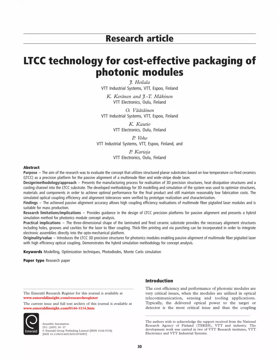
fabricate ceramic based components and modules(Paumanok, 2003). The key advantages of LTCC are costefficiency, high layer count, good dimensional control ofstructures, low loss at millimeter wave frequencies,compatibility with hermetic sealing and the possibility tointegrate electrical passives into the wiring board.The fabrication of a multilayer ceramic substrate by the use
of low temperature co-fired ceramics technology, LTCC, isshown in Figure 1. First, glass ceramic sheets are blanked andthen punched in order to form via holes. Secondly, via holesare metallized to form electrical interconnects between layers.The next step is patterning of electrical conductors andpassive circuits onto each layer by the use of screen printing orphoto imaging. The final steps are layer lamination, firingbellow 9808C temperatures and circuit dicing. Relatively lowsintering temperature allows the use of metal conductormaterials, such as, silver and gold. The system-on-chip (SOC)is finished by assembling discrete devices into the substrate.LTCC material has the capability of meeting the most
demanding electronic packaging and interconnectsrequirements. The technology is well established for bothhigh-performance applications such as those in military andspace applications, and high-volume cost sensitiveapplications such as those in the automotive and portablewireless industries. Cost-effective packaging solutions musthave fine feature patterning capability, high thermaldissipation and the flexibility to reliably interconnect bareand packaged ICs using variety of technologies. In addition,innovative integrated packaging will require mixing of analog,digital, RF and optical technologies and embedded passivecomponents and functions within multilayer substrates.For photonics and sensor applications, the ability to create
3D precision structures on the LTCC substrate is a veryimportant feature. Open cavities can be made on the surfacesof the LTCC substrate for the mounting of discretesemiconductor devices; buried cavities or channels can bemanufactured inside the substrate for fluidistics applications;accurate through hole structures are useful for photonicpackaging. More info about LTCC can be found from theweb sites: www.vtt.fi/ele/research/ope/micro_modules.htmand www.ltcc.de.
Design and modeling
The modelling of the passive laser-to-fiber coupling utilizingLTCC test substrates was started by performing toleranceanalysis modelling to several laser-to-fiber coupling pairs
Figure 1 Standard LTCC process
LTCC technology for cost-effective packaging of photonic modules
J.Heilala et al.
Assembly Automation
Volume 25 · Number 1 · 2005 · 30–37
31
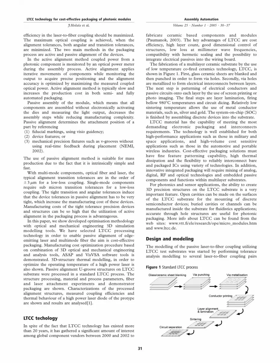
using ASAPe[2] optical design and simulation software. Anexample of modelling of an edge-emitting stripe laser opticalpower coupling to multimode fiber using a ball lens is shownin Figure 2.The coupling efficiency simulation results of several butt-
coupled laser-to-fiber pairs, and laser-to-fiber couplingutilizing 250 and 500mm ball lens were studied to limit thesolution space, more details can be found from Keranen et al.(2004).The tolerance analysis consists of sensitivity analysis
simulation and Monte-Carlo tolerance simulation. In thesensitivity analysis each tolerance variable is simulated asseparate and the most critical tolerance variables are found,which enables system optimization. In the Monte-Carlotolerancing all tolerance variables are simulatedsimultaneously and statistical information of the systemperformance is obtained.In Table I sensitivity analysis of a 1 £ 100mm laser and a
62.5/125mm graded-index multimode fiber is shown. AGaussian single mode beam model has been used in thesimulation. The values are as mm or degrees.From Table I we can see that the nominal coupling
efficiency is about 0.48. The most critical tolerance is source ydivergence, if the source power fluctuation is not noticed.Other important tolerances are source x divergence, fibernumerical aperture (NA), fiber core diameter and source ydecentering.Monte-Carlo cumulative distribution of butt-coupled 1 £
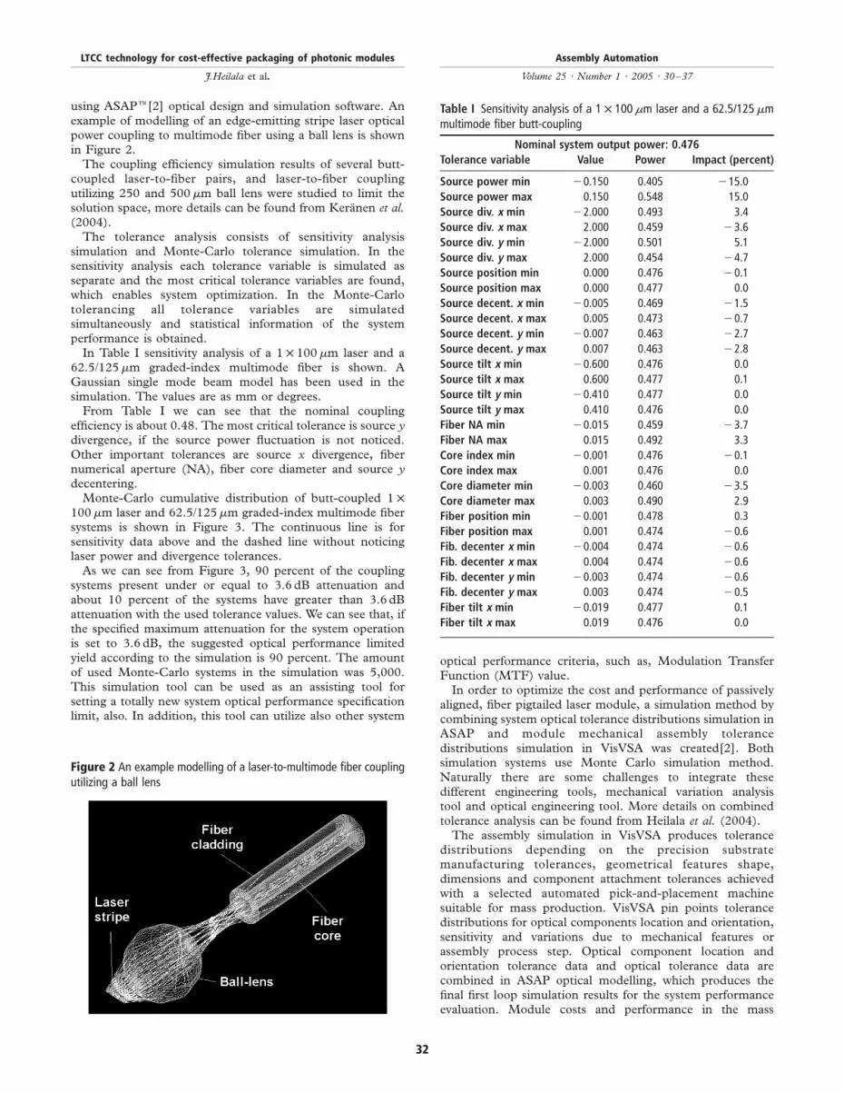
100mm laser and 62.5/125mm graded-index multimode fibersystems is shown in Figure 3. The continuous line is forsensitivity data above and the dashed line without noticinglaser power and divergence tolerances.As we can see from Figure 3, 90 percent of the coupling
systems present under or equal to 3.6 dB attenuation andabout 10 percent of the systems have greater than 3.6 dBattenuation with the used tolerance values. We can see that, ifthe specified maximum attenuation for the system operationis set to 3.6 dB, the suggested optical performance limitedyield according to the simulation is 90 percent. The amountof used Monte-Carlo systems in the simulation was 5,000.This simulation tool can be used as an assisting tool forsetting a totally new system optical performance specificationlimit, also. In addition, this tool can utilize also other system
optical performance criteria, such as, Modulation TransferFunction (MTF) value.In order to optimize the cost and performance of passively
aligned, fiber pigtailed laser module, a simulation method bycombining system optical tolerance distributions simulation inASAP and module mechanical assembly tolerancedistributions simulation in VisVSA was created[2]. Bothsimulation systems use Monte Carlo simulation method.Naturally there are some challenges to integrate thesedifferent engineering tools, mechanical variation analysistool and optical engineering tool. More details on combinedtolerance analysis can be found from Heilala et al. (2004).The assembly simulation in VisVSA produces tolerance
distributions depending on the precision substratemanufacturing tolerances, geometrical features shape,dimensions and component attachment tolerances achievedwith a selected automated pick-and-placement machinesuitable for mass production. VisVSA pin points tolerancedistributions for optical components location and orientation,sensitivity and variations due to mechanical features orassembly process step. Optical component location andorientation tolerance data and optical tolerance data arecombined in ASAP optical modelling, which produces thefinal first loop simulation results for the system performanceevaluation. Module costs and performance in the mass
Table I Sensitivity analysis of a 1 £ 100mm laser and a 62.5/125mmmultimode fiber butt-coupling
Nominal system output power: 0.476
Tolerance variable Value Power Impact (percent)
Source power min 20.150 0.405 215.0
Source power max 0.150 0.548 15.0
Source div. x min 22.000 0.493 3.4
Source div. x max 2.000 0.459 23.6
Source div. y min 22.000 0.501 5.1
Source div. y max 2.000 0.454 24.7
Source position min 0.000 0.476 20.1
Source position max 0.000 0.477 0.0
Source decent. x min 20.005 0.469 21.5
Source decent. x max 0.005 0.473 20.7
Source decent. y min 20.007 0.463 22.7
Source decent. y max 0.007 0.463 22.8
Source tilt x min 20.600 0.476 0.0
Source tilt x max 0.600 0.477 0.1
Source tilt y min 20.410 0.477 0.0
Source tilt y max 0.410 0.476 0.0
Fiber NA min 20.015 0.459 23.7
Fiber NA max 0.015 0.492 3.3
Core index min 20.001 0.476 20.1
Core index max 0.001 0.476 0.0
Core diameter min 20.003 0.460 23.5
Core diameter max 0.003 0.490 2.9
Fiber position min 20.001 0.478 0.3
Fiber position max 0.001 0.474 20.6
Fib. decenter x min 20.004 0.474 20.6
Fib. decenter x max 0.004 0.474 20.6
Fib. decenter y min 20.003 0.474 20.6
Fib. decenter y max 0.003 0.474 20.5
Fiber tilt x min 20.019 0.477 0.1
Fiber tilt x max 0.019 0.476 0.0
Figure 2 An example modelling of a laser-to-multimode fiber couplingutilizing a ball lens
LTCC technology for cost-effective packaging of photonic modules
J.Heilala et al.
Assembly Automation
Volume 25 · Number 1 · 2005 · 30–37
32
production can be optimized by performing an iterativeprocess, in which certain tolerances with the components andthe assembly produces certain simulated performancedistribution. Optical performance limited yield is definedthrough the simulated performance distribution.The process model used in the optimization of the module
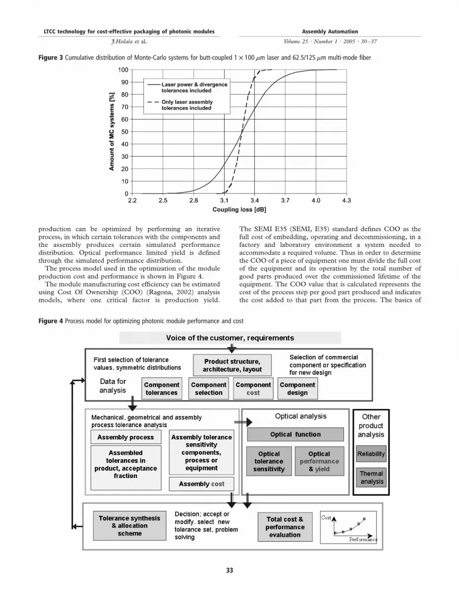
production cost and performance is shown in Figure 4.The module manufacturing cost efficiency can be estimated
using Cost Of Ownership (COO) (Ragona, 2002) analysismodels, where one critical factor is production yield.
The SEMI E35 (SEMI, E35) standard defines COO as thefull cost of embedding, operating and decommissioning, in afactory and laboratory environment a system needed toaccommodate a required volume. Thus in order to determinethe COO of a piece of equipment one must divide the full costof the equipment and its operation by the total number ofgood parts produced over the commissioned lifetime of theequipment. The COO value that is calculated represents thecost of the process step per good part produced and indicatesthe cost added to that part from the process. The basics of
Figure 3 Cumulative distribution of Monte-Carlo systems for butt-coupled 1 £ 100mm laser and 62.5/125mm multi-mode fiber
Figure 4 Process model for optimizing photonic module performance and cost
LTCC technology for cost-effective packaging of photonic modules
J.Heilala et al.
Assembly Automation
Volume 25 · Number 1 · 2005 · 30–37
33
COO are quite simple and can be summed up in the equation:COO ¼ Total costs/Total number of good parts.Normally the yield should be maximized in order to obtain
best COO value, but this typically considers the allocation todefective and correct modules. In this example, this is not thecase, but the simulated yield depends on the opticalperformance limit setting in the specification. All themanufactured modules can be seen as operational, but allare not exceeding the specified performance limit, such ascoupling efficiency between laser and fiber or delivered opticalpower from the fiber end. Naturally all modules are notnecessarily functional due to bonding failures and otherproduction errors in the manufacturing process. These factorsare noticed, however, in the definition of the final yield in themanufacturing. Our methodology can be used for theoptimization of cost and performance in the simulatedproduction. Simulated performance distribution of themodules can suggest the most cost-effective performancelimit location.
Thermal analysis
Another very important characteristic of a photonic module isits reliability. A low-cost module with high performance is notnecessarily adequate for market needs, if the modulereliability is poor. Operation temperature of the photonicdevice, such as laser diode, is probably the main criticalfactor. Efficient thermal control techniques are needed, whenhigh-power lasers are utilized in applications requiring highaverage power. High operation temperature of the devicecombined with moisture and oxygen is normally verydamaging combination to a laser diode. Therefore, in orderto ensure long-term reliability of photonic modules, hermeticsealing of the sensitive components is needed. LTCC isadvantageous substrate material for hermetic sealing due tothe fact that it is intrinsically hermetic and sensitivecomponents can be hermetically sealed individually to thesubstrate.Thermal control with high-power lasers is also essential due
to the fact that the laser diode operating point shifts, when thediode warms-up. The operation point can drift over aoperating point in which increasing the laser diode drivingpower does not increase optical power at all, but all the usedpower increases only the temperature of the diode creating avicious circle.In our work several thermal 3D structures on LTCC
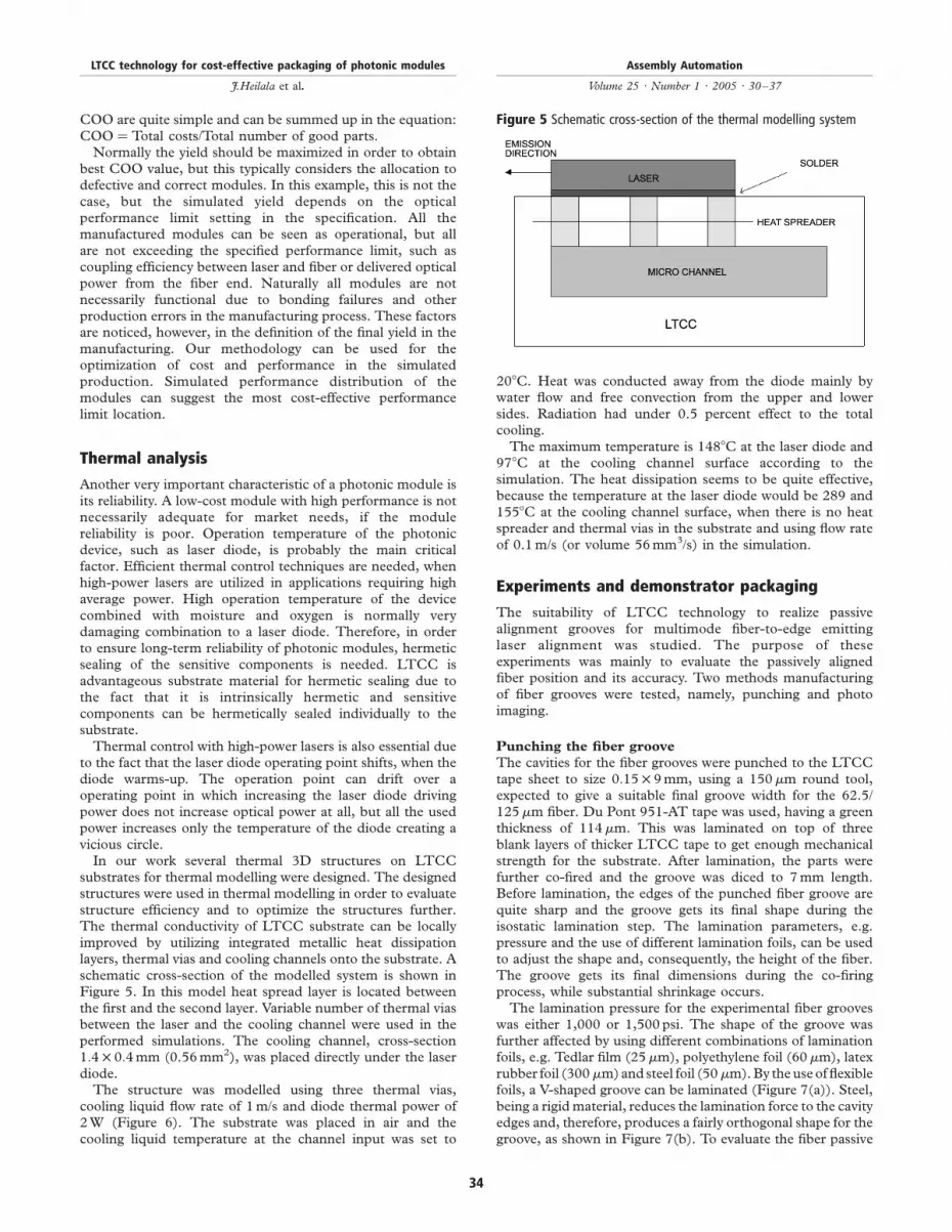
substrates for thermal modelling were designed. The designedstructures were used in thermal modelling in order to evaluatestructure efficiency and to optimize the structures further.The thermal conductivity of LTCC substrate can be locallyimproved by utilizing integrated metallic heat dissipationlayers, thermal vias and cooling channels onto the substrate. Aschematic cross-section of the modelled system is shown inFigure 5. In this model heat spread layer is located betweenthe first and the second layer. Variable number of thermal viasbetween the laser and the cooling channel were used in theperformed simulations. The cooling channel, cross-section1:4 £ 0:4mm (0.56mm2), was placed directly under the laserdiode.The structure was modelled using three thermal vias,
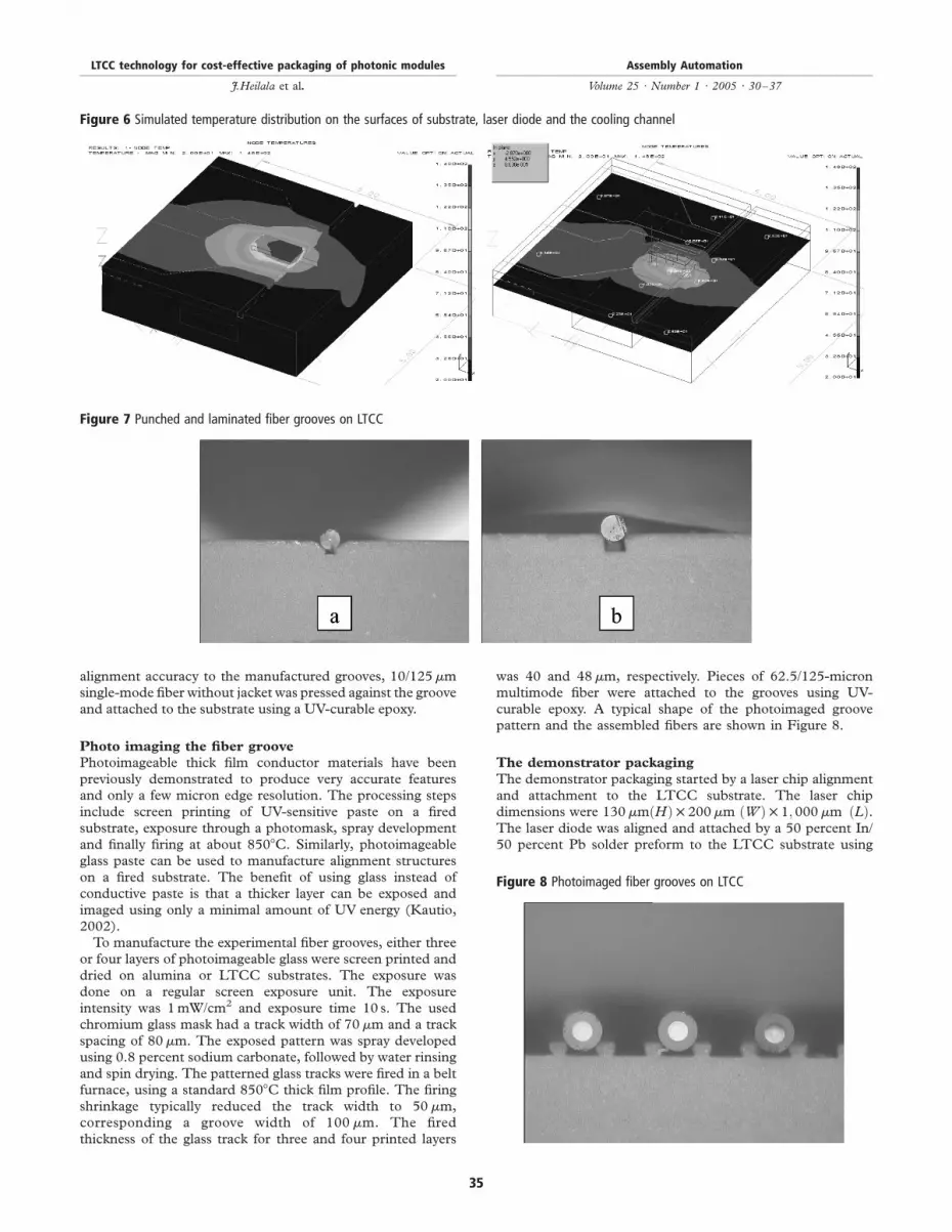
cooling liquid flow rate of 1m/s and diode thermal power of2W (Figure 6). The substrate was placed in air and thecooling liquid temperature at the channel input was set to
208C. Heat was conducted away from the diode mainly bywater flow and free convection from the upper and lowersides. Radiation had under 0.5 percent effect to the totalcooling.The maximum temperature is 1488C at the laser diode and
978C at the cooling channel surface according to thesimulation. The heat dissipation seems to be quite effective,because the temperature at the laser diode would be 289 and1558C at the cooling channel surface, when there is no heatspreader and thermal vias in the substrate and using flow rateof 0.1m/s (or volume 56mm3/s) in the simulation.
Experiments and demonstrator packaging
The suitability of LTCC technology to realize passivealignment grooves for multimode fiber-to-edge emittinglaser alignment was studied. The purpose of theseexperiments was mainly to evaluate the passively alignedfiber position and its accuracy. Two methods manufacturingof fiber grooves were tested, namely, punching and photoimaging.
Punching the fiber groove
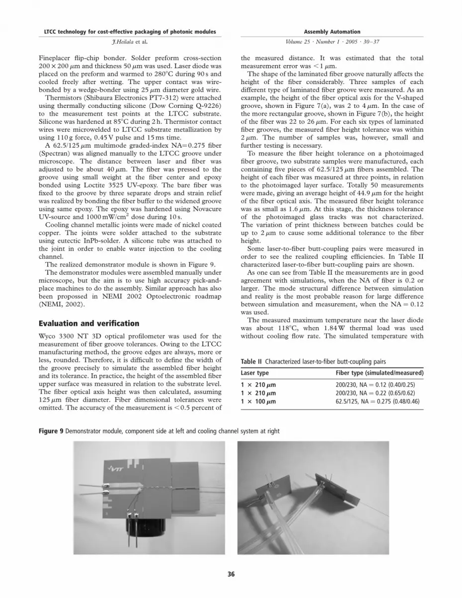
The cavities for the fiber grooves were punched to the LTCCtape sheet to size 0:15 £ 9mm, using a 150mm round tool,expected to give a suitable final groove width for the 62.5/125mm fiber. Du Pont 951-AT tape was used, having a greenthickness of 114mm. This was laminated on top of threeblank layers of thicker LTCC tape to get enough mechanicalstrength for the substrate. After lamination, the parts werefurther co-fired and the groove was diced to 7mm length.Before lamination, the edges of the punched fiber groove arequite sharp and the groove gets its final shape during theisostatic lamination step. The lamination parameters, e.g.pressure and the use of different lamination foils, can be usedto adjust the shape and, consequently, the height of the fiber.The groove gets its final dimensions during the co-firingprocess, while substantial shrinkage occurs.The lamination pressure for the experimental fiber grooves
was either 1,000 or 1,500 psi. The shape of the groove wasfurther affected by using different combinations of laminationfoils, e.g. Tedlar film (25mm), polyethylene foil (60mm), latexrubber foil (300mm)and steel foil (50mm).By theuse of flexiblefoils, a V-shaped groove can be laminated (Figure 7(a)). Steel,being a rigidmaterial, reduces the lamination force to the cavityedges and, therefore, produces a fairly orthogonal shape for thegroove, as shown in Figure 7(b). To evaluate the fiber passive
Figure 5 Schematic cross-section of the thermal modelling system
LTCC technology for cost-effective packaging of photonic modules
J.Heilala et al.
Assembly Automation
Volume 25 · Number 1 · 2005 · 30–37
34
alignment accuracy to the manufactured grooves, 10/125mmsingle-mode fiber without jacket was pressed against the grooveand attached to the substrate using a UV-curable epoxy.
Photo imaging the fiber groove
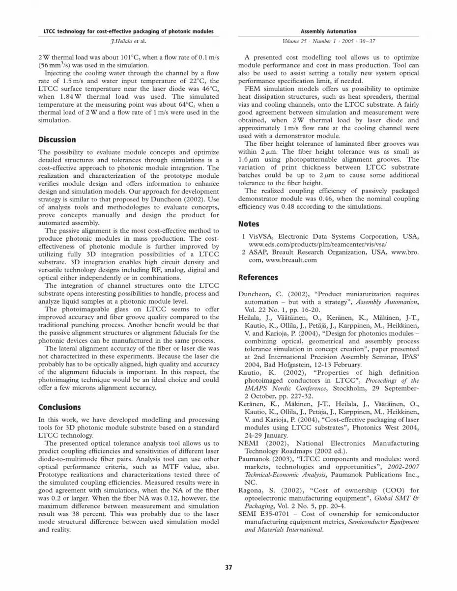
Photoimageable thick film conductor materials have beenpreviously demonstrated to produce very accurate featuresand only a few micron edge resolution. The processing stepsinclude screen printing of UV-sensitive paste on a firedsubstrate, exposure through a photomask, spray developmentand finally firing at about 8508C. Similarly, photoimageableglass paste can be used to manufacture alignment structureson a fired substrate. The benefit of using glass instead ofconductive paste is that a thicker layer can be exposed andimaged using only a minimal amount of UV energy (Kautio,2002).To manufacture the experimental fiber grooves, either three
or four layers of photoimageable glass were screen printed anddried on alumina or LTCC substrates. The exposure wasdone on a regular screen exposure unit. The exposureintensity was 1mW/cm2 and exposure time 10 s. The usedchromium glass mask had a track width of 70mm and a trackspacing of 80mm. The exposed pattern was spray developedusing 0.8 percent sodium carbonate, followed by water rinsingand spin drying. The patterned glass tracks were fired in a beltfurnace, using a standard 8508C thick film profile. The firingshrinkage typically reduced the track width to 50mm,corresponding a groove width of 100 mm. The firedthickness of the glass track for three and four printed layers
was 40 and 48mm, respectively. Pieces of 62.5/125-micronmultimode fiber were attached to the grooves using UV-curable epoxy. A typical shape of the photoimaged groovepattern and the assembled fibers are shown in Figure 8.
The demonstrator packaging
The demonstrator packaging started by a laser chip alignmentand attachment to the LTCC substrate. The laser chipdimensions were 130mmðHÞ £ 200mm ðW Þ £ 1; 000mm ðLÞ.The laser diode was aligned and attached by a 50 percent In/50 percent Pb solder preform to the LTCC substrate using
Figure 6 Simulated temperature distribution on the surfaces of substrate, laser diode and the cooling channel
Figure 7 Punched and laminated fiber grooves on LTCC
Figure 8 Photoimaged fiber grooves on LTCC
LTCC technology for cost-effective packaging of photonic modules
J.Heilala et al.
Assembly Automation
Volume 25 · Number 1 · 2005 · 30–37
35
Fineplacer flip-chip bonder. Solder preform cross-section200 £ 200mm and thickness 50mm was used. Laser diode wasplaced on the preform and warmed to 2808C during 90 s andcooled freely after wetting. The upper contact was wire-bonded by a wedge-bonder using 25mm diameter gold wire.Thermistors (Shibaura Electronics PT7-312) were attached
using thermally conducting silicone (Dow Corning Q-9226)to the measurement test points at the LTCC substrate.Silicone was hardened at 858C during 2 h. Thermistor contactwires were microwelded to LTCC substrate metallization byusing 110 g force, 0.45V pulse and 15ms time.A 62.5/125mm multimode graded-index NA¼0.275 fiber
(Spectran) was aligned manually to the LTCC groove undermicroscope. The distance between laser and fiber wasadjusted to be about 40mm. The fiber was pressed to thegroove using small weight at the fiber center and epoxybonded using Loctite 3525 UV-epoxy. The bare fiber wasfixed to the groove by three separate drops and strain reliefwas realized by bonding the fiber buffer to the widened grooveusing same epoxy. The epoxy was hardened using NovacureUV-source and 1000mW/cm2 dose during 10 s.Cooling channel metallic joints were made of nickel coated
copper. The joints were solder attached to the substrateusing eutectic InPb-solder. A silicone tube was attached tothe joint in order to enable water injection to the coolingchannel.The realized demonstrator module is shown in Figure 9.The demonstrator modules were assembled manually under
microscope, but the aim is to use high accuracy pick-and-place machines to do the assembly. Similar approach has alsobeen propossed in NEMI 2002 Optoelectronic roadmap(NEMI, 2002).
Evaluation and verification
Wyco 3300 NT 3D optical profilometer was used for themeasurement of fiber groove tolerances. Owing to the LTCCmanufacturing method, the groove edges are always, more orless, rounded. Therefore, it is difficult to define the width ofthe groove precisely to simulate the assembled fiber heightand its tolerance. In practice, the height of the assembled fiberupper surface was measured in relation to the substrate level.The fiber optical axis height was then calculated, assuming125mm fiber diameter. Fiber dimensional tolerances wereomitted. The accuracy of the measurement is ,0.5 percent of
the measured distance. It was estimated that the totalmeasurement error was ,1mm.The shape of the laminated fiber groove naturally affects the
height of the fiber considerably. Three samples of eachdifferent type of laminated fiber groove were measured. As anexample, the height of the fiber optical axis for the V-shapedgroove, shown in Figure 7(a), was 2 to 4mm. In the case ofthe more rectangular groove, shown in Figure 7(b), the heightof the fiber was 22 to 26mm. For each six types of laminatedfiber grooves, the measured fiber height tolerance was within2mm. The number of samples was, however, small andfurther testing is necessary.To measure the fiber height tolerance on a photoimaged
fiber groove, two substrate samples were manufactured, eachcontaining five pieces of 62.5/125mm fibers assembled. Theheight of each fiber was measured at three points, in relationto the photoimaged layer surface. Totally 50 measurementswere made, giving an average height of 44.9mm for the heightof the fiber optical axis. The measured fiber height tolerancewas as small as 1.6mm. At this stage, the thickness toleranceof the photoimaged glass tracks was not characterized.The variation of print thickness between batches could beup to 2mm to cause some additional tolerance to the fiberheight.Some laser-to-fiber butt-coupling pairs were measured in
order to see the realized coupling efficiencies. In Table IIcharacterized laser-to-fiber butt-coupling pairs are shown.As one can see from Table II the measurements are in good
agreement with simulations, when the NA of fiber is 0.2 orlarger. The mode structural difference between simulationand reality is the most probable reason for large differencebetween simulation and measurement, when the NA ¼ 0.12was used.The measured maximum temperature near the laser diode
was about 1188C, when 1.84W thermal load was usedwithout cooling flow rate. The simulated temperature with
Figure 9 Demonstrator module, component side at left and cooling channel system at right
Table II Characterized laser-to-fiber butt-coupling pairs
Laser type Fiber type (simulated/measured)
1 3 210mm 200/230, NA ¼ 0.12 (0.40/0.25)
1 3 210mm 200/230, NA ¼ 0.22 (0.65/0.62)
1 3 100mm 62.5/125, NA ¼ 0.275 (0.48/0.46)
LTCC technology for cost-effective packaging of photonic modules
J.Heilala et al.
Assembly Automation
Volume 25 · Number 1 · 2005 · 30–37
36
2W thermal load was about 1018C, when a flow rate of 0.1m/s(56mm3/s) was used in the simulation.Injecting the cooling water through the channel by a flow
rate of 1.5m/s and water input temperature of 228C, theLTCC surface temperature near the laser diode was 468C,when 1.84W thermal load was used. The simulatedtemperature at the measuring point was about 648C, when athermal load of 2W and a flow rate of 1m/s were used in thesimulation.
Discussion
The possibility to evaluate module concepts and optimizedetailed structures and tolerances through simulations is acost-effective approach to photonic module integration. Therealization and characterization of the prototype moduleverifies module design and offers information to enhancedesign and simulation models. Our approach for developmentstrategy is similar to that proposed by Duncheon (2002). Useof analysis tools and methodologies to evaluate concepts,prove concepts manually and design the product forautomated assembly.The passive alignment is the most cost-effective method to
produce photonic modules in mass production. The cost-effectiveness of photonic module is further improved byutilizing fully 3D integration possibilities of a LTCCsubstrate. 3D integration enables high circuit density andversatile technology designs including RF, analog, digital andoptical either independently or in combinations.The integration of channel structures onto the LTCC
substrate opens interesting possibilities to handle, process andanalyze liquid samples at a photonic module level.The photoimageable glass on LTCC seems to offer
improved accuracy and fiber groove quality compared to thetraditional punching process. Another benefit would be thatthe passive alignment structures or alignment fiducials for thephotonic devices can be manufactured in the same process.The lateral alignment accuracy of the fiber or laser die was
not characterized in these experiments. Because the laser dieprobably has to be optically aligned, high quality and accuracyof the alignment fiducials is important. In this respect, thephotoimaging technique would be an ideal choice and couldoffer a few microns alignment accuracy.
Conclusions
In this work, we have developed modelling and processingtools for 3D photonic module substrate based on a standardLTCC technology.The presented optical tolerance analysis tool allows us to
predict coupling efficiencies and sensitivities of different laserdiode-to-multimode fiber pairs. Analysis tool can use otheroptical performance criteria, such as MTF value, also.Prototype realizations and characterizations tested three ofthe simulated coupling efficiencies. Measured results were ingood agreement with simulations, when the NA of the fiberwas 0.2 or larger. When the fiber NA was 0.12, however, themaximum difference between measurement and simulationresult was 38 percent. This was probably due to the lasermode structural difference between used simulation modeland reality.
A presented cost modelling tool allows us to optimizemodule performance and cost in mass production. Tool canalso be used to assist setting a totally new system opticalperformance specification limit, if needed.FEM simulation models offers us possibility to optimize
heat dissipation structures, such as heat spreaders, thermalvias and cooling channels, onto the LTCC substrate. A fairlygood agreement between simulation and measurement wereobtained, when 2W thermal load by laser diode andapproximately 1m/s flow rate at the cooling channel wereused with a demonstrator module.The fiber height tolerance of laminated fiber grooves was
within 2mm. The fiber height tolerance was as small as1.6mm using photopatternable alignment grooves. Thevariation of print thickness between LTCC substratebatches could be up to 2mm to cause some additionaltolerance to the fiber height.The realized coupling efficiency of passively packaged
demonstrator module was 0.46, when the nominal couplingefficiency was 0.48 according to the simulations.
Notes
1 VisVSA, Electronic Data Systems Corporation, USA,www.eds.com/products/plm/teamcenter/vis/vsa/
2 ASAP, Breault Research Organization, USA, www.bro.com, www.breault.com
References
Duncheon, C. (2002), “Product miniaturization requiresautomation – but with a strategy”, Assembly Automation,Vol. 22 No. 1, pp. 16-20.
Heilala, J., Vaatainen, O., Keranen, K., Makinen, J-T.,Kautio, K., Ollila, J., Petaja, J., Karppinen, M., Heikkinen,V. and Karioja, P. (2004), “Design for photonics modules –combining optical, geometrical and assembly processtolerance simulation in concept creation”, paper presentedat 2nd International Precision Assembly Seminar, IPAS’2004, Bad Hofgastein, 12-13 February.
Kautio, K. (2002), “Properties of high definitionphotoimaged conductors in LTCC”, Proceedings of theIMAPS Nordic Conference, Stockholm, 29 September-2 October, pp. 227-32.
Keranen, K., Makinen, J-T., Heilala, J., Vaatainen, O.,Kautio, K., Ollila, J., Petaja, J., Karppinen, M., Heikkinen,V. and Karioja, P. (2004), “Cost-effective packaging of lasermodules using LTCC substrates”, Photonics West 2004,24-29 January.
NEMI (2002), National Electronics ManufacturingTechnology Roadmaps (2002 ed.).
Paumanok (2003), “LTCC components and modules: wordmarkets, technologies and opportunities”, 2002-2007Technical-Economic Analysis, Paumanok Publications Inc.,NC.
Ragona, S. (2002), “Cost of ownership (COO) foroptoelectronic manufacturing equipment”, Global SMT &Packaging, Vol. 2 No. 5, pp. 20-4.
SEMI E35-0701 – Cost of ownership for semiconductormanufacturing equipment metrics, Semiconductor Equipmentand Materials International.
LTCC technology for cost-effective packaging of photonic modules