288
| Date post: | 01-Feb-2023 |
| Category: |
Documents |
| Upload: | khangminh22 |
| View: | 0 times |
| Download: | 0 times |


Materials Science-Poland, Vol. 26, No. 4, 2008
MAG-EL-MAT. A summary
B. IDZIKOWSKI*
Institute of Molecular Physics, Polish Academy of Sciences, ul. M. Smoluchowskiego 17, 60-179 Poznań, Poland
The Scientific Network New materials for magnetoelectronics – MAG-EL-MAT was founded in the beginning of 2003 and its activity was concluded in the first half of 2008. The network gathered over 50 very active research groups, i.e., about 300 scien-tists from Polish universities and other scientific institutions (mostly from the Polish Academy of Sciences), its general theoretical and experimental goal being to investi-gate the electronic and magnetic properties of novel materials exhibiting properties useful for creation of new magnetoelectronic devices.
The first MAG-EL-MAT Members Meeting, held in Będlewo between 26 and 28 October 2003, gathered 43 participants from 16 Polish institutions, who appointed the Coordinating Committee, got acquainted with the main programme of the Network and briefly presented the institutions they represented, the main research topics and fields of possible collaboration.
The second meeting on 13–16 April 2004 gathered about 70 members and was di-vided into 11 short sessions. Nine invited lectures, 17 oral contributions and 9 posters were presented; additionally, 7 special talks were given on the achievements of Cen-tres of Excellence affiliated to various MAG-EL-MAT institutions and on the oppor-tunities available within the framework of the EU programmes.
The number of participants taking part in the third Members Meeting on 2–6 May, 2005, organised into 7 scientific sessions, increased to 102 members and guests. The participants listened to a plenary lecture given by J. Spałek, 11 invited lectures and 21 oral contributions. Thirty eight posters were also presented. For the first time, the or-ganizers decided to print the conference contributions in a regular journal. 50 papers were selected for publication in a special issue of Materials Science-Poland [1].
The fourth Members Meeting took place on 3–6 May, 2006 in the form of a series of small seminars (four special sessions) and a plenary session with plenary lectures delivered by J. Kossut and J. Dubowik. The topics selected for the fourth MAG-EL -MAT meeting were biomagnetics and medical physics, strongly correlated electrons __________
*E-mail: [email protected]
B. IDZIKOWSKI 804
in spintronics, modern electronics and nanotechnology. The number of participants increased to 104, with 27 oral presentations and 60 posters. Fifty papers were pub-lished in the post-meeting issue of Materials Science-Poland [2].
In 2007, Mathematical Research and Conference Centre of the Polish Academy of Sciences in w Będlewo and its environs were chosen again for the venue of the fifth Members Meeting (7–10 May 2007). The scientific sessions were devoted to magnetic oxides and intermetallics, surfaces, interfaces, films and layered structures, as well as to quantum transport and quantum computing. The last session of the meeting, entitled Unusual materials, unusual properties was more interdisciplinary. A pleasant and memorable meeting in the full springtime Będlewo, far from the city noise, brought together 117 participants. Twenty five oral contributions and 73 posters were pre-sented at the meeting (because of a large number of contributions, two poster sessions were scheduled). Interesting plenary lectures were delivered by J. Korecki and P. Pierański.
This time, as the final collection of post- MAG-EL-MAT members Meeting papers, 63 manuscripts have been selected – more than could be placed in a single issue of Materials Science-Poland. At the request of the Publisher, 20 from the accepted pa-pers were published in earlier issues of the journal [3, 4]. The present issue of Materi-als Science-Poland, concluding the series of post-MAG-EL-MAT publications, con-tains 41 papers. Moreover, 5 selected papers have also been published in Acta Physica Polonica A [5].
We are very grateful to all authors for submitting the manuscripts and to all scien-tists who acted as referees (sometimes it was a difficult job) for their efforts aiming at improving the quality of the papers.
Finally, it is my sad duty to inform the readers that Professor Henryk K. Lachowicz (member of the MAG-EL-MAT Coordinating Committee) will no longer be with us as he has passed away in August 2006. This issue of Materials Science-Poland is dedi-cated to his memory.
References
[1] Materials Science-Poland, 24 (2006), No. 3, 539–874. [2] Materials Science-Poland, 25 (2007), No. 2, 261–602. [3] Materials Science-Poland, 25 (2007), No. 4, 1223–1294. [4] Materials Science-Poland, 26 (2008), No. 3, 693–765. [5] Acta Physica Polonica A, 113 (2008), No. 2, 641–668.
Received 11 August 2008
Materials Science-Poland, Vol. 26, No. 4, 2008
Magnetocaloric effect. Physics and applications
H. SZYMCZAK*, R. SZYMCZAK
Institute of Physics, Polish Academy of Sciences, Warszawa 02-668, Poland
The principles of magnetic cooling and the magnetocaloric properties of various magnetic com-pounds have been presented with a special focus on materials with giant and colossal magnetocaloric parameters. The magnetocaloric properties of manganites and cobaltites have been considered. The max-imum entropy change in polycrystalline La0.7Ca0.3MnO3 for the field of 2 T reaches 8 J·kg–1·K–1, exceed-ing that of gadolinium. It is suggested that the manganites with superior magnetocaloric properties and low material costs are attractive magnetic refrigerator materials for technical applications.
Key words: magnetocaloric effect; entropy; phase transition; magnetic refrigerator
1. Introduction
The magnetocaloric effect is characterized by an adiabatic change in temperature T (or an isothermal change in entropy, ΔS) arising from the application of external magnetic field H. Recently, one can note an increased interest in this more than 100-year old phenomenon (see review papers [1–7]). The magnetocaloric effect arises due to the presence of two energy reservoirs in magnetic materials: one with phonon and the other with magnon excitations. These two reservoirs are coupled by the spin-lattice (in other words – magnetoelastic) interactions. An external magnetic field affects the spin degrees of freedom resulting in heating or cooling of magnetic materials. This simple description of the magnetocaloric effect indicates that the highest change in tempera-ture is expected for strongly magnetostrictive magnetic materials. The magnetocaloric effect increases with increase of the applied magnetic field and with the change of magnetization M(T,H) during application of magnetic field. This means that the effect reaches its maximum in the vicinity of magnetic phase transition points.
The magnetocaloric effect in various magnetic materials, summarized in the men-tioned review papers, will be briefly considered. The present review will be primarily concerned with the recent results of the magnetocaloric studies of manganites and
__________
*Corresponding author, e-mail: [email protected]
H. SZYMCZAK, R. SZYMCZAK 808
cobaltites. The possibility of use of these materials in magnetic refrigerators will also be discussed.
2. Giant and colossal magnetocaloric effects
During isothermal magnetization processes, the total magnetic entropy change ΔSH of the magnetic system due to the application of a magnetic field H is given by [5, 6]:
( )0
,H
HH
MS T H dHT
∂⎛ ⎞Δ = ⎜ ⎟∂⎝ ⎠∫ (1)
The adiabatic temperature change ΔTad(T,H) can be determined using the experi-mentally measured heat capacity C(T,H):
( )0
, ( , )
H
adH
M TT T H dHT C T H
∂⎛ ⎞ ′Δ = ⎜ ⎟ ′∂⎝ ⎠∫ (2)
Since MH
∂∂
has its maximum at the transition point, a large magnetocaloric effect
is expected near the transition temperature. It is exceedingly high (“giant” or “colos-sal”) for the first order phase transition. The upper limit for the molar magnetic entro-py variation is given by the magnetic contribution [4, 5]: ( )maxΔ ln 2 1MS R J= + (3)
where R is the gas constant and J is the total angular momentum of the magnetic ion. Though the magnetocaloric effect was first discovered in iron [7], research on
practical application of this phenomenon has been for years concentrated on gadoli-nium rare earth metal with a large |ΔSH| parameter (5 J·kg–1·K–1 for ΔH= 2 T) at room temperature. Unfortunately, this material is very expensive. Therefore, numerous ex-perimental studies have been focused on the search for new magnetic materials that are cheaper but exhibit magnetocaloric effect larger than Gd. In 1997, a giant magne-tocaloric effect was discovered in Gd2Si2Ge2 [8], a compound with |ΔSH| considerably higher (27 J·kg–1·K–1 for ΔH = 2 T) than that in Gd. This material exhibits a first order magnetic transition coupled to a martensitic-like, displacive structural transition from an orthorhombic to a monoclinic phase [9].
Another important type of magnetocaloric materials are MnAs based compounds. The base material MnAs undergoes a combined structural and ferro-paramagnetic transition of the first order with |ΔSH|= 32 J·kg–1·K–1 at ΔH = 2 T near room tempera-ture [10].The colossal magnetocaloric effect was discovered in MnAs under hydro-static pressure [11]. In this case |ΔSH| reaches values up to 267 J·kg–1·K–1 for ΔH = 2 T, T = 281 K and p = 2.23 kbar. In molar terms, it results in a value of 34.7 J·K–1·mol–1, 1.47 times greater than the theoretical limit ΔSmax determined according to Eq. (3). The origin of this colossal magnetocaloric effect is the contribution to the entropy variation
Magnetocaloric effect 809
coming from strong magnetoelastic interactions. The strong magnetoelastic interaction is the driving force for structural and first order magnetic phase transitions. The phe-nomenological model of the colossal magnetocaloric effect in MnAs was recently developed by von Ranke et al. [12]. The model confirms the fundamental role of the lattice entropy in the colossal magnetocaloric effect for the MnAs based compounds. In some cases, there exists a full analogy between external pressure and chemical pressure. Because of a small difference in the atomic radii, it is expected that the sub-stitution of Fe for Mn should emulate the pressure effect in MnAs [13]. The colossal magnetocaloric effect at ambient pressure in Mn1–xFexAs for x = 0.003 reaches values up to 330 J·kg–1·K–1 for ΔH= 5 T. Important point is that Fe doping does not change the density of states at the Fermi level in the host compound.
3. Giant magnetocaloric effect in manganites
In recent years, there has been increasing interest in using manganites not only as materials with a colossal magnetoresistivity but also as materials with interesting magnetocaloric properties. Such a proposition was made more than 10 years ago by Zhang et al. [14] who performed magnetocaloric measurements in La0.67Ca0.33MnO3 and La0.60Ca0.33Y0.07MnO3. In next years, many other manganites have been examined from this point of view (see [5, 6, and 15] for references). A large magnetocaloric effect makes manganites excellent candidates for working materials in magnetic refri-geration units especially because they are less costly than any other materials, particu-larly those based on Gd.
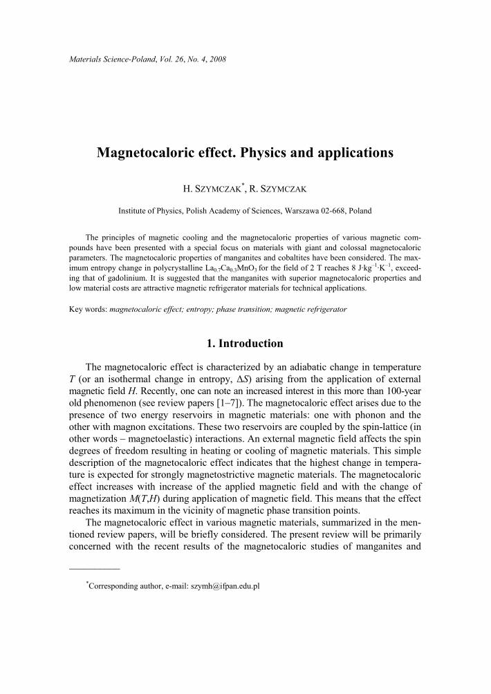
Fig. 1. Temperature dependence of the susceptibility for La0.65Ca0.35MnO3 polycrystals in low field (20 Oe) for field cooling (FC) and zero field cooling (ZFC) regimes
H. SZYMCZAK, R. SZYMCZAK 810
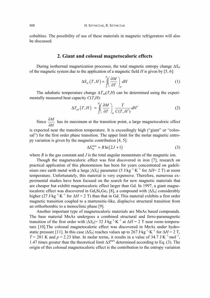
Fig. 2. Change of the magnetic entropy of La0.65Ca0.35MnO3 polycrystals in function of temperature at fixed values of the external magnetic field
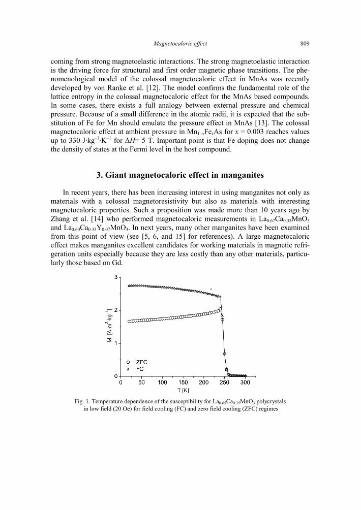
Fig. 3. Temperature dependence of susceptibility for La0.7Ca0.3MnO3 polycrystals in low field (20 Oe) for field cooling (FC) and zero field cooling (ZFC) regimes
Recently, we have shown [16] that the changes in entropy near TC depend strongly on various extrinsic factors. These dependences suggest that the magnitude of the magnetocaloric effect should depend strongly on methods of sample preparation. We have performed detailed studies of the magnetocaloric effect for La1–xCaxMnO3 with x = 0.3, 0.35 and 0.4 prepared by a nonstandard ceramic method. It was shown that the sharpness of the paramagnetic to ferromagnetic transition increases with Ca doping. It is seen in Fig. 1 that this transition is very sharp in La0.65Ca0.35MnO3 polycrystals. Al-though the sharp transition indicates a first-order phase transition, the M vs. H depen-dences exhibit no anomalies characteristic of this type of transition. It is interesting that for almost the same level of doping in La0.67Ca0.33MnO3, the paramagnetic-ferro-
Magnetocaloric effect 811
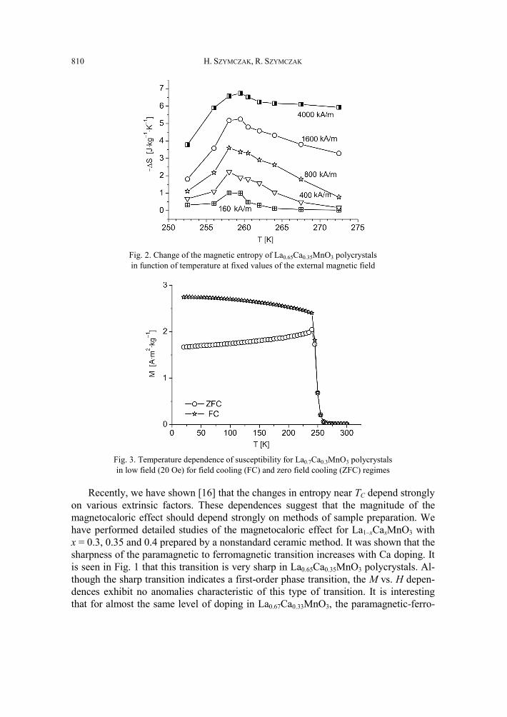
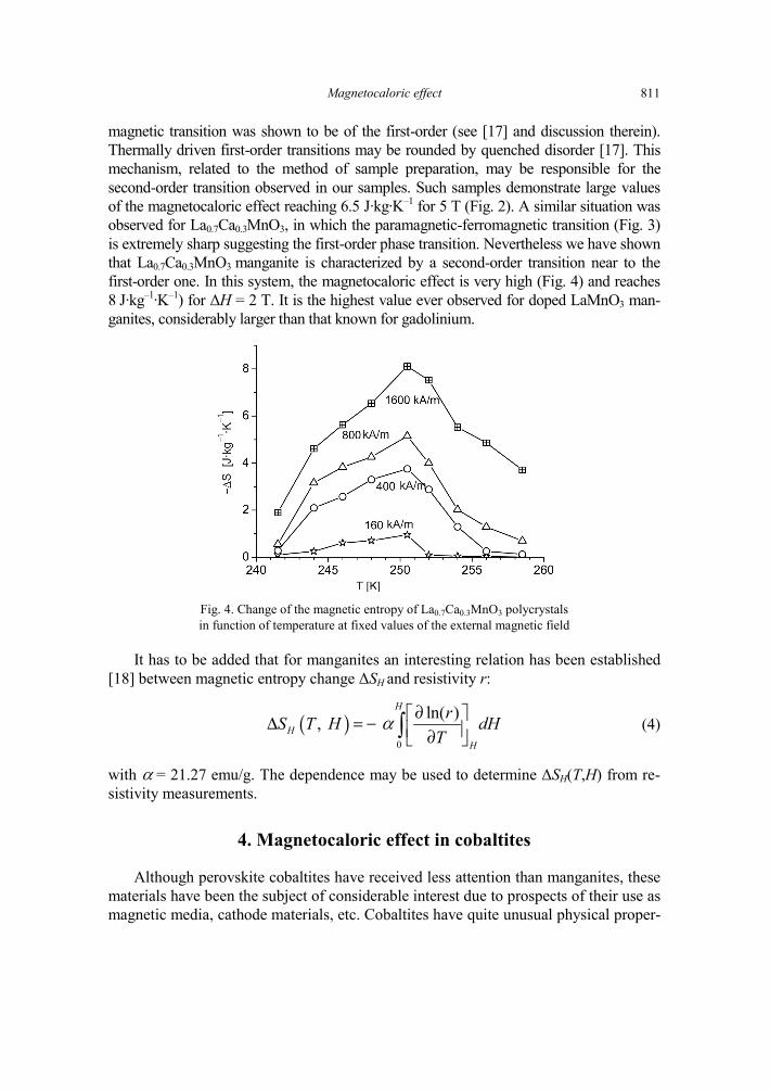
magnetic transition was shown to be of the first-order (see [17] and discussion therein). Thermally driven first-order transitions may be rounded by quenched disorder [17]. This mechanism, related to the method of sample preparation, may be responsible for the second-order transition observed in our samples. Such samples demonstrate large values of the magnetocaloric effect reaching 6.5 J·kg·K–1 for 5 T (Fig. 2). A similar situation was observed for La0.7Ca0.3MnO3, in which the paramagnetic-ferromagnetic transition (Fig. 3) is extremely sharp suggesting the first-order phase transition. Nevertheless we have shown that La0.7Ca0.3MnO3 manganite is characterized by a second-order transition near to the first-order one. In this system, the magnetocaloric effect is very high (Fig. 4) and reaches 8 J·kg–1·K–1) for ΔH = 2 T. It is the highest value ever observed for doped LaMnO3 man-ganites, considerably larger than that known for gadolinium.
Fig. 4. Change of the magnetic entropy of La0.7Ca0.3MnO3 polycrystals in function of temperature at fixed values of the external magnetic field
It has to be added that for manganites an interesting relation has been established [18] between magnetic entropy change ΔSH and resistivity r:
( )0
ln( ), H
HH
rS T H dHT
α ∂⎡ ⎤Δ = − ⎢ ⎥∂⎣ ⎦∫ (4)
with α = 21.27 emu/g. The dependence may be used to determine ΔSH(T,H) from re-sistivity measurements.
4. Magnetocaloric effect in cobaltites
Although perovskite cobaltites have received less attention than manganites, these materials have been the subject of considerable interest due to prospects of their use as magnetic media, cathode materials, etc. Cobaltites have quite unusual physical proper-
H. SZYMCZAK, R. SZYMCZAK 812
ties. Co3+ ions can occur in three different spin configurations: low-spin (S = 0), inter-mediate-spin (S = 1) or high-spin (S = 2) states. It is generally agreed upon that ther-mal excitation in cobaltites may induce spin-state transitions. In addition to these spin -state phenomena, magnetoelectronic phase separation occurs in cobaltites upon dop-ing. All these features make the magnetocaloric effect in cobaltites completely different from that in manganites.
Fig. 5. Change of the magnetic entropy of a La0.8Ca0.2CoO3 single crystal in function of temperature at fixed values of the external magnetic field
Fig. 6. Change of the magnetic entropy of a Tb0.9Dy0.1BaCo2O5.5 single crystal
in function of temperature at fixed values of the external magnetic field
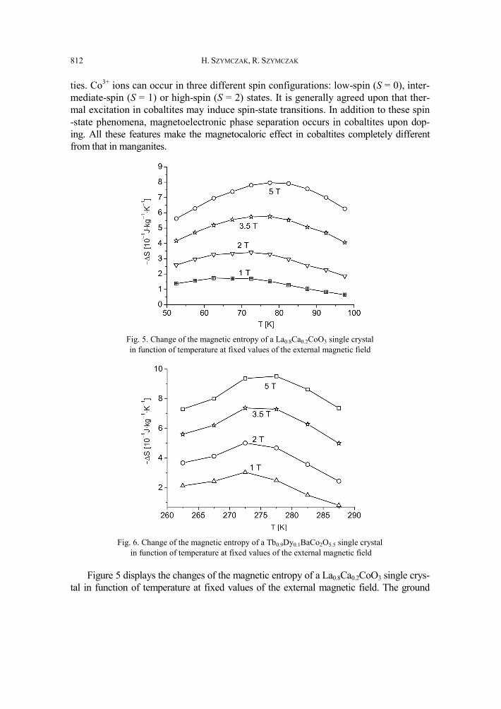
Figure 5 displays the changes of the magnetic entropy of a La0.8Ca0.2CoO3 single crys-tal in function of temperature at fixed values of the external magnetic field. The ground
Magnetocaloric effect 813
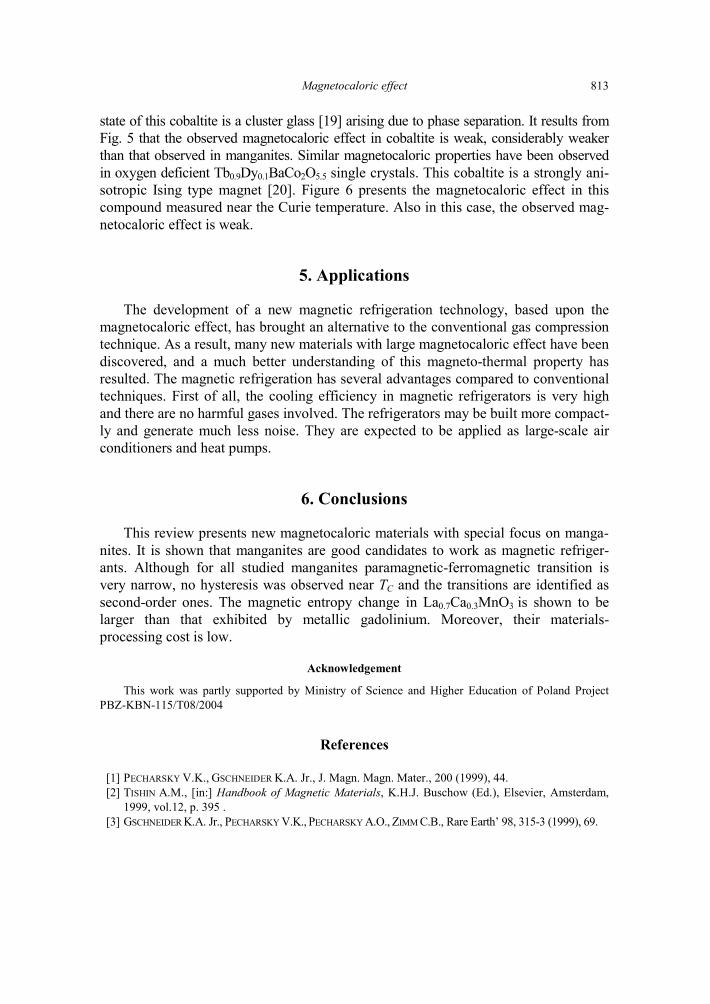
state of this cobaltite is a cluster glass [19] arising due to phase separation. It results from Fig. 5 that the observed magnetocaloric effect in cobaltite is weak, considerably weaker than that observed in manganites. Similar magnetocaloric properties have been observed in oxygen deficient Tb0.9Dy0.1BaCo2O5.5 single crystals. This cobaltite is a strongly ani-sotropic Ising type magnet [20]. Figure 6 presents the magnetocaloric effect in this compound measured near the Curie temperature. Also in this case, the observed mag-netocaloric effect is weak.
5. Applications
The development of a new magnetic refrigeration technology, based upon the magnetocaloric effect, has brought an alternative to the conventional gas compression technique. As a result, many new materials with large magnetocaloric effect have been discovered, and a much better understanding of this magneto-thermal property has resulted. The magnetic refrigeration has several advantages compared to conventional techniques. First of all, the cooling efficiency in magnetic refrigerators is very high and there are no harmful gases involved. The refrigerators may be built more compact-ly and generate much less noise. They are expected to be applied as large-scale air conditioners and heat pumps.
6. Conclusions
This review presents new magnetocaloric materials with special focus on manga-nites. It is shown that manganites are good candidates to work as magnetic refriger-ants. Although for all studied manganites paramagnetic-ferromagnetic transition is very narrow, no hysteresis was observed near TC and the transitions are identified as second-order ones. The magnetic entropy change in La0.7Ca0.3MnO3 is shown to be larger than that exhibited by metallic gadolinium. Moreover, their materials-processing cost is low.
Acknowledgement
This work was partly supported by Ministry of Science and Higher Education of Poland Project PBZ-KBN-115/T08/2004
References
[1] PECHARSKY V.K., GSCHNEIDER K.A. Jr., J. Magn. Magn. Mater., 200 (1999), 44. [2] TISHIN A.M., [in:] Handbook of Magnetic Materials, K.H.J. Buschow (Ed.), Elsevier, Amsterdam,
1999, vol.12, p. 395 . [3] GSCHNEIDER K.A. Jr., PECHARSKY V.K., PECHARSKY A.O., ZIMM C.B., Rare Earth’ 98, 315-3 (1999), 69.
H. SZYMCZAK, R. SZYMCZAK 814
[4] TISHIN A.M., SPICHKIN Y.I., The Magnetocaloric Effect and its Applications, Inst. Phys. Publ., Bris-tol, 2003.
[5] GSCHNEIDER K.A. Jr., PECHARSKY V.K, TSOKOL A.O., Rep. Prog. Phys., 68 (2005), 1479. [6] PHAN M.-H, YU S.-C., J. Magn. Magn. Mater., 306 (2007), 325. [7] BRUCK E., J.Phys. D: Appl.Phys., 38 (2005), R381. [8] PECHARSKY V.K., GSCHNEIDER K.A. Jr., Phys. Rev. Letters 78 (1997), 4494. [9] PAUDYAL D., PECHARSKY V.K., GSCHNEIDER K.A. Jr., HARMON B.N., Phys. Rev., B 73 (2006),
144406. [10] WADA H., TANABE Y., Appl. Phys. Lett., 79 (2001), 3302. [11] GAMA S., COELHO A.A., DE CAMPOS A., CARVALHO M.G., GANDRA F.C.G., VON RANKE P.J.,
DE OLIVEIRA N.A., Phys. Rev. Lett., 93 (2004), 237202. [12] RANKE P.J., GAMA S., COELHO A.A., DE CAMPOS A., CARVALHO M.G., GANDRA F.C.G.,
DE OLIVEIRA N.A., Phys.Rev,. B 73 (2006), 014415. [13] DE CAMPOS A.,.ROCCO D.L, CARVALHO M.G., CARON L., COELHO A.A., GAMA S., DA SILVA L.M.,
GANDRA F.C.G., DOS SANTOS A.O., CARDOSO L.P., RANKE P.J., DE OLIVEIRA N.A., Nature Mater., 5 (2006), 802.
[14] ZHANG X.X., TEJADA J., XIN Y., SUN G.F., WONG K.W., BOHIGAS X., Appl. Phys. Lett., 69 (1996), 3596. [15] SZEWCZYK A., SZYMCZAK H., WISNIEWSKI A., PIOTROWSKI K., KARTASZYNSKI R., DABROWSKI B.,
KOLESNIK S., BUKOWSKI Z., Appl. Phys. Lett., 77 (2000), 1026. [16] SZYMCZAK R., CZEPELAK M., KOLANO R., KOLANO-BURIAN A., KRZYMANSKA B., SZYMCZAK H.,
J. Mater. Sci., 43 (2008), 1734. [17] ROSSLER S. , ROSSLER U.K., NENKOV K., ECKERT D., YUSUF S.M., DORR K., MULLER K.-H., Phys.
Rev., B 70 (2004) 104417. [18] XIONG C.M., SUN J.R., CHEN Y.F., SHEN B.G., DU J., LI Y.X., IEEE Trans. Magn., 41 (2005), 122. [19] SZYMCZAK H.,BARAN M., BABONA G.J., DIDUSZKO R., FINK-FINOWICKI J.AND SZYMCZAK R.,
J. Magn. Magn. Mater., 285 (2005), 386. [20] BARAN M., GATALSKAYA V.I., SZYMCZAK R., SHIRYAEV S.V., BARILO S.N., BYCHKOV G.L., SZYM-
CZAK H., J.Phys.: Condens. Matter, 17 (2005), 5613.
Received 39 April 2007
Materials Science-Poland, Vol. 26, No. 4, 2008
Magnetism and electronic structures of hexagonal 1:1:1 rare earth-based intermetallic compounds
Ł. GONDEK1*, J. ŻUKROWSKI1, M. BAŁANDA2, D. KACZOROWSKI3, A. SZYTUŁA4
1Faculty of Physics and Applied Computer Science, AGH University of Science and Technology, 30-059 Cracow, Poland
2H. Niewodniczański Institute of Nuclear Physics, Polish Academy of Sciences, 31-342 Cracow, Poland 3W. Trzebiatowski Institute of Low Temperature and Structure Research,
Polish Academy of Sciences, Wrocław 50-950, Poland 4 M. Smoluchowski Institute of Physics, Jagiellonian University, 30-059 Cracow, Poland
Correlations between magnetic properties and electronic structure of rare earth based intermetallics of the ZrNiAl-type crystal structure have been analysed. The analysis has been supported by results of magnetometric, neutron diffraction and photoelectron spectroscopy measurements. It has been demon-strated that structure of the valence band and crystal electric field effects are the most important factors affecting the magnetic behaviour of the discussed compounds.
Key words: magnetic properties; electronic structure; rare earth compounds
1. Introduction
Rare earth based intermetallics of RTX stoichiometry (R – rare earth, T – d-elect- ron element, X – p-electron element), crystallizing with the ZrNiAl-type crystal struc-ture exhibit a great variety of intriguing physical properties. Ce-based compounds of CeTX composition have attracted special interest due to their unusual magnetic behav-iour driven mainly by hybridisation of the 4f states with the conduction bands [1–4]. Dominance of the Kondo effect over the RKKY interactions results in non-magnetic ground states in CeNiAl [5, 6], CeNiIn [3, 7], CePdIn [4], CePtIn [8] or CeRhSn [9]. Otherwise, long-range magnetically ordered phases (CeCuAl [6], CeAuIn [7]) are observed. In weakly hybridized Ce- and Nd-based ZrNiAl-type phases, the crystal field (CF) splitting of ground multiplets leads to formation of magnetic CF doublet
__________ *Corresponding author; e-mail: [email protected]
Ł. GONDEK et al. 816
ground states. An opposite situation occurs in the case of PrTX compounds, where intrinsically non-magnetic CF singlet ground state is expected. However, some Pr-based RTX compounds exhibit long-range magnetic order (as found, e.g., in PrNiAl [10, 11] and PrCuAl [12]). This is possible when energies of excited CF levels are comparable to exchange interaction energy. Apart from the CF effects, the hybridisa-tion of Pr 4f states with T nd states may result in absence of any magnetic order (es-tablished for PrPdIn [13], PrPtSn [14], PrRhSn [9]). For compounds with heavy rare earths (Gd–Er), the magnetic order is rather common. As non-magnetic exceptions HoRhSn and ErRhSn may be given [14].
2. Crystal structure
About one third of known RTX compounds crystallize in the ZrNiAl-type struc-ture (space group No. 189). Within this crystal structure the atoms occupy the follow-ing positions: R at 3(f) site: (–xR,– xR, 0), (xR, 0, 0), (0, xR, 0), T at 1(a) site: (0, 0, 0) and 2(d) site: (1/3, 2/3, 1/2), (2/3, 1/3, 1/2) and X at 3(g) site: (–xX, –xX, 1/2), (xX, 0, 1/2), (0, xX, 1/2).
This hexagonal system is very interesting as it induces topological frustration of magnetic interactions due to triangular coordination of rare earth magnetic ions lying within ab-planes. These well separated planes may be considered as quasi two-dimensional. Recently, magnetic phase diagram of the ZrNiAl lattice has been investi-gated by means of XY model yielding the existence at T = 0 of three different long-range ordered phases [15]. Another interesting feature of the ZrNiAl lattice is that, according to group symmetry analysis, not all magnetic ions must belong to the same orbit symmetry [16].
3. Magnetic properties and electronic structure
3.1 Influence of d-electron element (T)
Among the RTX compounds crystallising in the ZrNiAl-type structure the indides family has been comprehensively studied till now [17]. Within this family, RNiIn, RPdIn and RAuIn series exhibit the most interesting magnetic properties. Magnetism in these compounds seems to be mostly influenced by Ni 3d, Pd 4d and Au 5d states lying in the valence band. The authors focused on some selected Pr-based compounds, as their magnetic properties are not satisfactorily known.
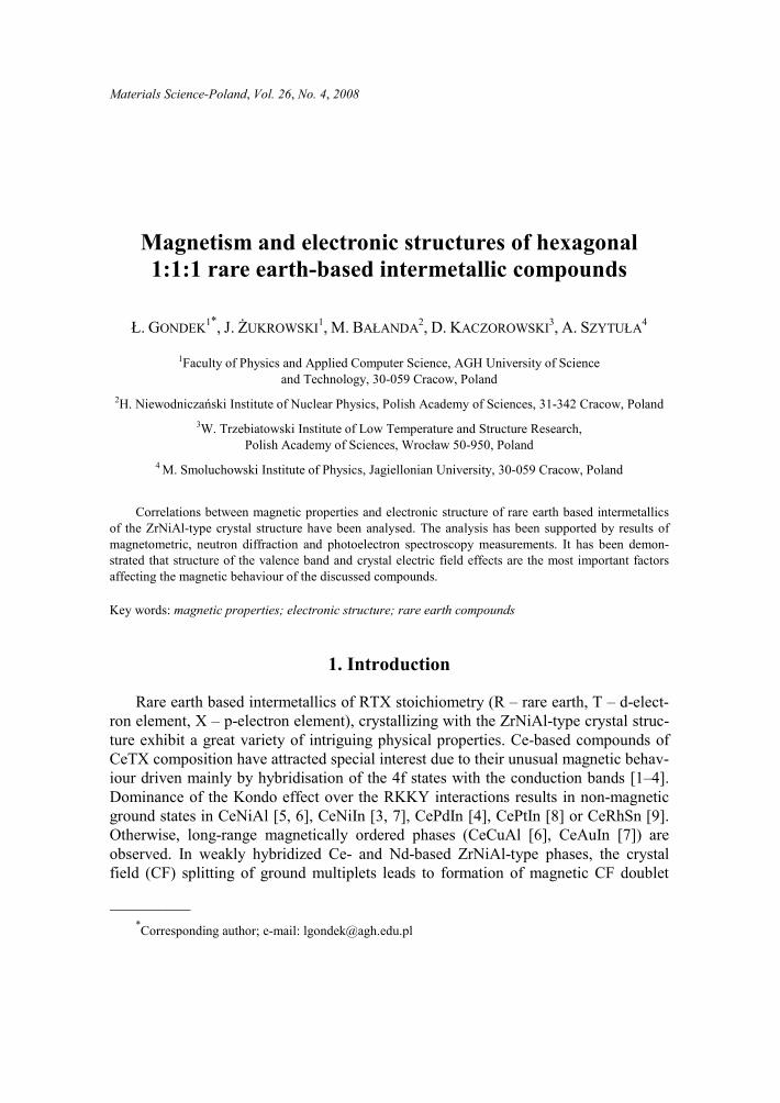
The magnetic susceptibilities of PrTIn (T = Ni, Pd, Au) samples do not indicate any magnetic ordering down to low temperatures (see Fig. 1a). In Figure 1b, the va-lence bands of PrTIn compounds are presented. Similarly to most RNiIn compounds [18], the Ni 3d states are located just below the Fermi level (FL). The relatively high
Magnetism and electronic structures of rare earth-based intermetallic compounds 817
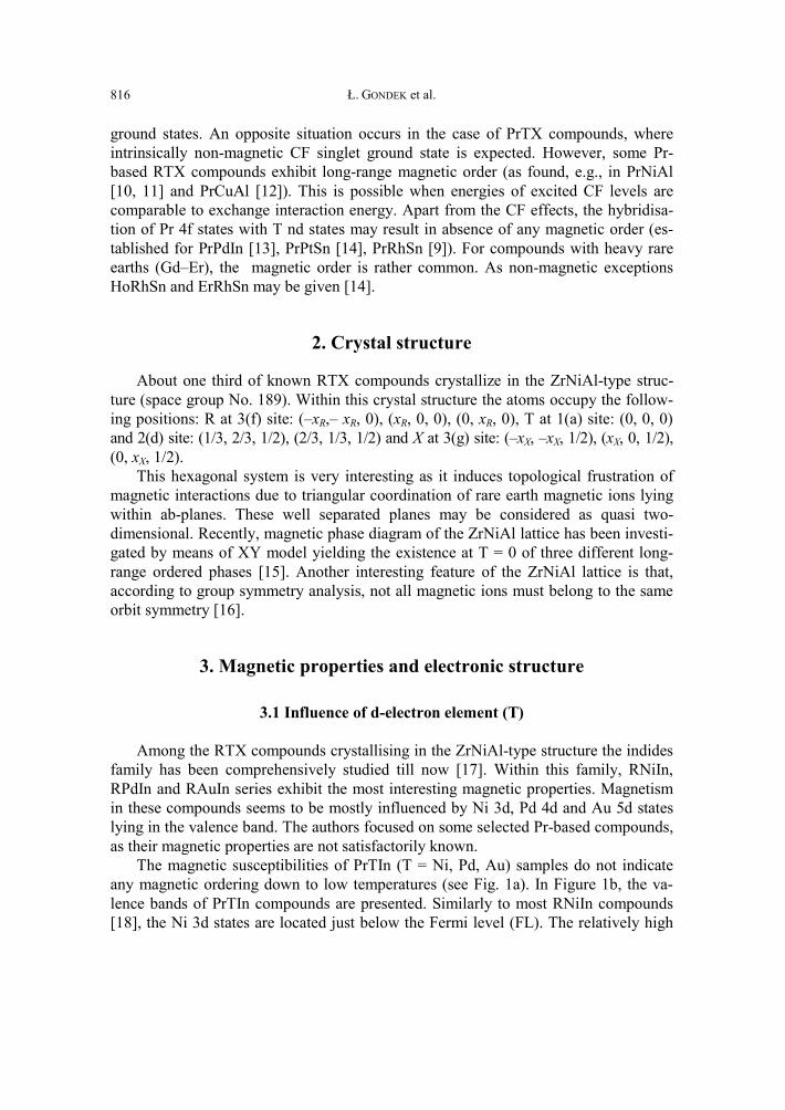
density of states (DOS) at the FL is reflected in high ordering temperatures which follow the de Gennes scaling (Fig. 2). No magnetic ordering was found for CeNiIn (Kondo lattice) and for PrNiIn. In both cases, the R 4f–Ni 3d hybridisation is the key factor to understand the non-magnetic behaviour. The Ce 4f states are located at about 2 eV below the FL, while the Pr 4f ones are at about 3 eV, and these states heavily overlap with the Ni 3d ones. The magnetic order appears in NdNiIn, where the separa-tion between the Nd 4f and Ni 3d states is notably larger.
Fig. 1. Magnetic properties and valence bands structures of selected RTIn compounds:
a) low temperature magnetic susceptibility of PrTIn phases, b) PrTIn valence band spectra (solid lines) with estimated contribution of Pr 4f states (dotted lines), c) influence of T element on the valence band spectra for non stoichiometric TbNixAu1–xIn compounds
Fig. 2. De Gennes scaling for selected RTX compounds
The RPdIn family exhibits magnetic properties similar to the RNiIn series. In this case, the Pd 4d states are shifted a bit deeper below the Fermi level (~3.8 eV), how-ever DOS at the FL is similar to the RNiIn case. Thus, the ordering temperatures of the RPdIn compounds are comparable to those of RNiIn (see Fig. 2). Overlap of the
Ł. GONDEK et al. 818
Pd 4d states with the Pr 4f ones is larger than that with the Ce 4f or Nd 4f states (Fig. 1b). Consequently, PrPdIn does not exhibit magnetic ordering down to 1.7 K, opposite to the Ce- and Nd-based analogues [13].
The magnetic behaviour of the RAuIn family is different from the before-discussed cases. While the maximum of Au 5d states lies about 5 eV below the Fermi level, the DOS at the FL is significantly lower than that in RNiIn and RPdIn. This is clearly reflected in the valence band spectra of the TbNi0.4Au0.6In and TbNi0.6Au0.4In solid solutions (Fig. 1c). The ordering temperatures of the RAuIn phases are much lower than those of the Ni- or Pd-based compounds, and they do not obey the de Gennes scaling (Fig. 2). These findings indicate rather small coupling of the 4f elec-trons with the valence band. Thus, CeAuIn is a simple antiferromagnetic metal. For PrAuIn and NdAuIn, no magnetic ordering was observed, however the main reason for such behaviour is different in each case. In Pr-based indide, the hybridization be-tween the Pr 4f and Au 5d states is not considered to be significant due to their large energetic separation. In turn, the magnetic susceptibility of this compound shows some kind of plateau at low temperatures, being indicative of singlet CF ground state (Fig. 1a). In contrast, the CF effect cannot be responsible for non-magnetic behaviour of NdAuIn, because of the expected Kramers doublet of CF ground state. Apparently, in this compound it is the hybridisation between the Nd 4f and Au 5d states which makes it non-magnetic. The Nd 4f states strongly overlap with the Au 5d ones, as both are located at about 5 eV below the FL. Within the RAuIn family, the TbAuIn indide exhibits the most interesting magnetic properties; for this compound an unusual se-quence of magnetic transitions: paramagnet – spin-glass – antiferromagnet has been found [19].
3.2 Influence of p-electron element (X)
In order to relate magnetic properties of the RTX compounds to the kind of the p-electron element, two families of the RNiAl and RNiIn compounds can be chosen. In both series, similar ordering temperatures are observed, as the DOS at the FL origi-nates mainly from the Ni 3d states. Moreover, similar valence band structures, i.e. similar 4f3d hybridisation strength imply that mainly the CF effects are responsible for different magnetic behaviour in these compounds.
For example, whereas PrNiIn is non-magnetic, PrNiAl exhibits antiferomagnetism below 6.5 K [10, 11]. In the latter compound, the excitation energy between the CF singlet ground state and the next CF levels is significantly lower than that in the in-dide. In TbNiAl and TbNiIn antiferromagnets, the ordered magnetic moments lie along the c axis and the ab plane, respectively [20, 21]. This essential difference is certainly due to CF induced anisotropy, as from the topological point of view the alignment within the ab plane is energetically more preferable in the case of anti-ferromagnetic interactions [15].
Magnetism and electronic structures of rare earth-based intermetallic compounds 819
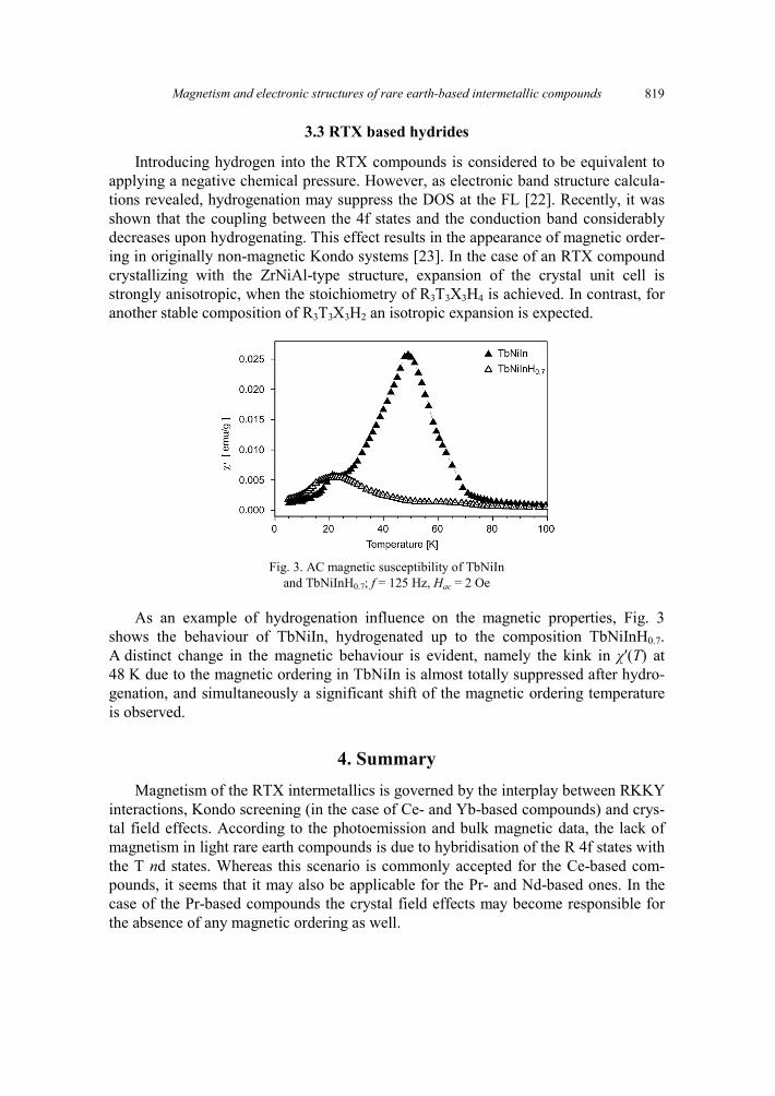
3.3 RTX based hydrides
Introducing hydrogen into the RTX compounds is considered to be equivalent to applying a negative chemical pressure. However, as electronic band structure calcula-tions revealed, hydrogenation may suppress the DOS at the FL [22]. Recently, it was shown that the coupling between the 4f states and the conduction band considerably decreases upon hydrogenating. This effect results in the appearance of magnetic order-ing in originally non-magnetic Kondo systems [23]. In the case of an RTX compound crystallizing with the ZrNiAl-type structure, expansion of the crystal unit cell is strongly anisotropic, when the stoichiometry of R3T3X3H4 is achieved. In contrast, for another stable composition of R3T3X3H2 an isotropic expansion is expected.
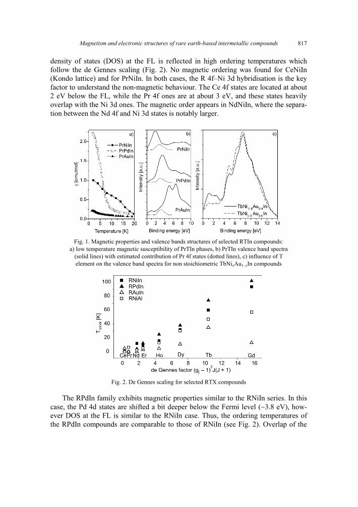
Fig. 3. AC magnetic susceptibility of TbNiIn and TbNiInH0.7; f = 125 Hz, Hac = 2 Oe
As an example of hydrogenation influence on the magnetic properties, Fig. 3 shows the behaviour of TbNiIn, hydrogenated up to the composition TbNiInH0.7. A distinct change in the magnetic behaviour is evident, namely the kink in χ′(T) at 48 K due to the magnetic ordering in TbNiIn is almost totally suppressed after hydro-genation, and simultaneously a significant shift of the magnetic ordering temperature is observed.
4. Summary Magnetism of the RTX intermetallics is governed by the interplay between RKKY
interactions, Kondo screening (in the case of Ce- and Yb-based compounds) and crys-tal field effects. According to the photoemission and bulk magnetic data, the lack of magnetism in light rare earth compounds is due to hybridisation of the R 4f states with the T nd states. Whereas this scenario is commonly accepted for the Ce-based com-pounds, it seems that it may also be applicable for the Pr- and Nd-based ones. In the case of the Pr-based compounds the crystal field effects may become responsible for the absence of any magnetic ordering as well.
Ł. GONDEK et al. 820
Acknowledgements
This work was partially supported by the Polish Ministry of Science and Higher Education within Grant No. 1P03B 11129.
References
[1] ADROJA D.T., MALIK S.K., J. Magn. Magn. Mater., 100 (1991), 126. [2] FUJITA T., SUZUKI T., NISHIGORI S., TAKABATAKE T., FUJII H., SAKURAI J., J. Magn. Magn. Mater.,
108 (1992), 35. [3] FUJII H., INOUE T., ANDOH Y., TAKABATAKE T., SATOH K., MAENO Y., FUJITA T., SAKURAI J.,
YAMAGUCHI Y., Phys. Rev., B 39 (1989), 6840. [4] SATOH K., MAENO Y., FUJITA T., UWATOKO Y., FUJII H., J. Phys. (Paris), 49 (1988), C8-779. [5] TUAN N.C., SECHOWSKY V., DIVIS M., SVOBODA P., NAKOTTE H., de BOER F.R., KIM-NGAN N.H.,
J. Appl. Phys., 73 (1993), 5677. [6] JAVORSKY P., CHERNYAVSKY A., SECHOVSKY V., Physica B, 281–282 (2000), 71. [7] GONDEK Ł., PENC B., SZYTUŁA A., JEZIERSKI A., ZYGMUNT A., Acta Phys. Polon. A, 34 (2003),
1209. [8] FUJITA T., SATOH K., MAENO Y., UWATOKO Y., FUJII H., J. Magn. Magn. Mater., 76–77 (1988), 133. [9] ROUTSI Ch.D., YAKINTHOS J.K., GAMARI-SEALE H., J. Magn. Magn. Mater., 117 (1992), 79.
[10] EHLERS G., MALETTA H., Z. Phys. B, 101 (1996), 317. [11] JAVORSKY P., SECHOVSKY V., ARONS R.R., BURLET P., RESSOUCHE E., SVOBODA P., LAPERTOT G.,
J. Magn. Magn. Mater., 164 (1996), 183. [12] JAVORSKY P., SECHOVSKY V., HAVELA L., MICHOR H., J. Magn. Magn. Mater., 177–181 (1998), 1052. [13] GONDEK Ł., SZYTUŁA A., KACZOROWSKI D., NENKOV K., Solid State Commun., 142 (2007), 556. [14] ROUTSI Ch.D., YAKINTHOS J.K., GAMARI-SEALE H., J. Magn. Magn. Mater., 110 (1992), 317. [15] GONDEK Ł., SZYTUŁA A., J. Alloys. Comp., 442 (2007) 111. [16] JAVORSKY P., BURLET P., SECHOVSKY V., ANDREEV A.V., BROWN J., SVOBODA P., J. Magn. Magn.
Mater., 166 (1997), 133. [17] KALYCHAK Y.M., ZAREMBA V.I., POTTGEN R., LUKACHUK M., HOFFMANN R.D., Rare Earth-
Transition Metal-Indides, [in:] K.A. Gschneider, J.C.G. Bunzli, V.K. Pecharsky (Eds.), Handbook on the Physics and Chemistry of Rare Earths, Vol. 34, Elsevier, Amsterdam, 2005, p. 1.
[18] HÜFNER S., Photoelectron Spectroscopy, Springer, Berlin, 1995. [19] GONDEK Ł., SZYTUŁA A., BAŁANDA M., WARKOCKI W., SZEWCZYK A., GUTOWSKA M., Solid State
Commun. 136 (2005), 26. [20] GONDEK Ł., SZYTUŁA A., BARAN S., HERNANDEZ-VELASCO J., J. Magn. Magn. Mater., 272–276
(2004), e443. [21] EHLERS G., MALETTA H., Z. Phys. B, 99 (1996), 145. [22] VAJEESTON P., RAVINDRAN P., VIDYA R., KJEKSHUS A., FJELLVAG H., YARTYS V. A., Phys. Rev. B,
67 (2003), 14101. [23] CHEVALIER B., WATTIAUX A., BOBET J-L., J. Phys.: Condens. Matter, 18 (2006), 1743.
Received 25 April 2007
Materials Science-Poland, Vol. 26, No. 4, 2008
Strong electronic correlations in CePt4In
A. PIKUL*, D. KACZOROWSKI
Institute of Low Temperature and Structure Research, Polish Academy of Sciences, P.O. Box 1410, 50-950 Wrocław 2, Poland
Polycrystalline samples of CePt4In and LaPt4In were studied by means of X-ray powder diffraction, magnetic susceptibility, electrical resistivity and specific heat measurements. Some of the results have been compared to those reported previously for single-crystalline specimens. The physical properties of CePt4In indicate that the magnetic moments of cerium are rather well localized and contribute to the Kondo-type scattering of conduction electrons in the presence of strong crystalline electric field.
Key words: CePt4In; CeInPt4; strong electronic correlations; heavy fermion behaviour; Kondo effect
1. Introduction
Usual behaviour of strongly correlated electron systems (SCES) is a highlight of present-day condensed matter physics. The SCES intermetallics based on cerium, ytterbium or uranium have unfilled 4f or 5f electronic shell which strongly interacts (hybridizes) with conduction and/or valence band states of s-, p-, and d-type. Depend-ing on the strength of the f-ligand interactions, measured by the exchange integral Jkf [1], a variety of different low-temperature properties have been observed, spanning from long-range magnetic ordering, to formation of heavy quasi-particles (heavy fer-mions), and to fluctuating-valence state for low, intermediate and high values of Jkf, respectively. All these phenomena are directly related to the localization of f-electrons, namely the higher value of the exchange integral, the more delocalized character ex-hibit the f-electrons. In particular, in the intermediate-valence state they are only partly localized even at ambient temperatures.
For most compounds with well localized f-electrons, an important role of the crys-talline electric field (CEF) effect is recognised. In the case of stable Ce3+ ions placed in a cubic environment, the six-fold degenerated 2F5/2 ground level splits into a Γ7 dou-blet and a Γ8 quartet separated by an energy Δ being of the order of 100–300 K. Usually,
__________
*Corresponding author, e-mail: [email protected]
A. PIKUL, D. KACZOROWSKI 822
this phenomenon distinctly influences magnetic, thermodynamic and electrical-transport characteristics, studied as functions of temperature and magnetic field.
The cubic compound CePt4In was originally classified in the literature as a va-lence-fluctuation system with strongly enlarged electronic contribution to the specific heat (C/T ≈ 1.75 J·mol−1·K2 at 100 mK) and distinct CEF effect [2]. That interesting (yet physically rather questionable) coexistence of the opposing ground states moti-vated us to undertake comprehensive reinvestigations of physical properties of this particular compound. In the present paper, we briefly review and discuss hitherto ob-tained results of several experiments performed in wide ranges of temperature and magnetic field strength, on polycrystalline as well as on single-crystalline specimens.
2. Experimental
Polycrystalline samples of CePt4In and of its non-magnetic reference system LaPt4In were synthesized by conventional arc melting of stoichiometric amounts of the constituents (Pt foil, Ce and In pieces; purity 99.9%) under protective purified-argon atmosphere. The melted pellets were subsequently wrapped in molybdenum foil, sealed in evacuated silica tubes, and annealed at 900 °C for one month. The qual-ity of the final products was examined by X-ray powder diffraction using a commer-cial Stoe diffractometer (CuKα radiation, λ = 1.54056 Å) and by energy dispersive X-ray scattering (EDXS) analysis employing an EDAX PV9800 spectrometer attached to a Philips 515 scanning electron microscope.
High-quality single crystals of CePt4In were grown using a conventional flux method, using elemental lead as a flux. The starting components (Ce, Pt, In as above, Pb pieces: purity 99.9%) were weighed in the atomic ratio 1:4:1:20, loaded into an alumina crucible, and sealed in a quartz ampoule under argon gas pressure of about 0.3 atm. The mixture was first heated up to 1030 °C, held at this temperature for 2 h, and then cooled down to 400 °C at the rate of 1–2 °C/h and finally down to room tem-perature upon switching off the furnace. Several well-faceted polyhedra-shaped single crystals with dimensions up to 0.6 mm were isolated from the flux by etching Pb in a solution of acetic acid and hydrogen peroxide. Their quality was checked by X-ray diffraction using an Xcalibur CCD Oxford Diffraction four-circle diffractometer (graphite-monochromated MoKα radiation; λ = 0.71073 Å) and by microprobe EDXS analysis (equipment as above).
Magnetic properties of CePt4In and LaPt4In were studied at temperatures ranging from 1.9 K up to 300 K and in external magnetic fields up to 5 T using a commercial Quantum Design MPMS-5 SQUID magnetometer. Electrical resistivity measurements were performed in the range 4–300 K employing a conventional four-probe method, on bar-shaped specimens with spot-welded electrical contacts. The transverse (B ⊥ j) magnetoresistivity was measured below 30 K in external magnetic fields up to 8 T. The Seebeck coefficient was measured at temperatures from 5 K up to room tempera-
Strong electronic correlations in CePt4In 823
ture using a standard differential method with pure copper as a reference. Heat capac-ity measurements were carried out over the temperature interval 2–400 K, employing a thermal relaxation technique [3] implemented in a commercial Quantum Design PPMS-9 platform.
3. Results
3.1. Crystal structure
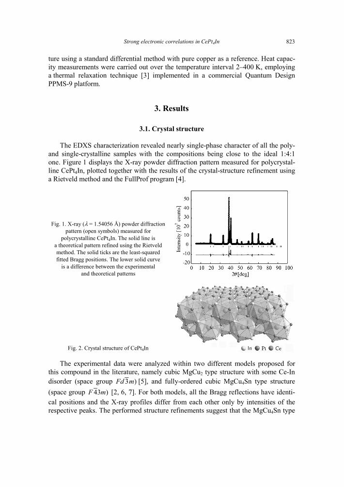
The EDXS characterization revealed nearly single-phase character of all the poly- and single-crystalline samples with the compositions being close to the ideal 1:4:1 one. Figure 1 displays the X-ray powder diffraction pattern measured for polycrystal-line CePt4In, plotted together with the results of the crystal-structure refinement using a Rietveld method and the FullProf program [4].
Fig. 1. X-ray (λ = 1.54056 Å) powder diffraction pattern (open symbols) measured for
polycrystalline CePt4In. The solid line is a theoretical pattern refined using the Rietveld method. The solid ticks are the least-squared fitted Bragg positions. The lower solid curve
is a difference between the experimental and theoretical patterns
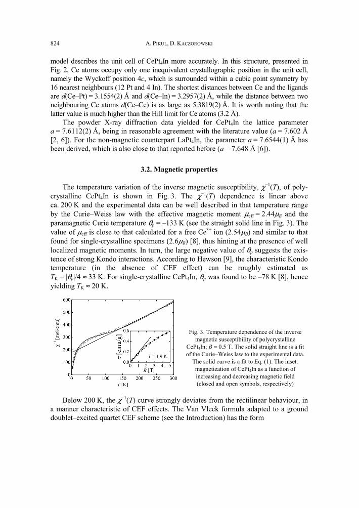
Fig. 2. Crystal structure of CePt4In
The experimental data were analyzed within two different models proposed for this compound in the literature, namely cubic MgCu2 type structure with some Ce-In disorder (space group 3 )Fd m [5], and fully-ordered cubic MgCu4Sn type structure (space group 43 )F m [2, 6, 7]. For both models, all the Bragg reflections have identi-cal positions and the X-ray profiles differ from each other only by intensities of the respective peaks. The performed structure refinements suggest that the MgCu4Sn type
A. PIKUL, D. KACZOROWSKI 824
model describes the unit cell of CePt4In more accurately. In this structure, presented in Fig. 2, Ce atoms occupy only one inequivalent crystallographic position in the unit cell, namely the Wyckoff position 4c, which is surrounded within a cubic point symmetry by 16 nearest neighbours (12 Pt and 4 In). The shortest distances between Ce and the ligands are d(Ce–Pt) = 3.1554(2) Å and d(Ce–In) = 3.2957(2) Å, while the distance between two neighbouring Ce atoms d(Ce–Ce) is as large as 5.3819(2) Å. It is worth noting that the latter value is much higher than the Hill limit for Ce atoms (3.2 Å).
The powder X-ray diffraction data yielded for CePt4In the lattice parameter a = 7.6112(2) Å, being in reasonable agreement with the literature value (a = 7.602 Å [2, 6]). For the non-magnetic counterpart LaPt4In, the parameter a = 7.6544(1) Å has been derived, which is also close to that reported before (a = 7.648 Å [6]).
3.2. Magnetic properties
The temperature variation of the inverse magnetic susceptibility, χ−1(T), of poly-crystalline CePt4In is shown in Fig. 3. The χ−1(T) dependence is linear above ca. 200 K and the experimental data can be well described in that temperature range by the Curie–Weiss law with the effective magnetic moment μeff = 2.44μB and the paramagnetic Curie temperature θp = –133 K (see the straight solid line in Fig. 3). The value of μeff is close to that calculated for a free Ce3+ ion (2.54μB) and similar to that found for single-crystalline specimens (2.6μB) [8], thus hinting at the presence of well localized magnetic moments. In turn, the large negative value of θp suggests the exis-tence of strong Kondo interactions. According to Hewson [9], the characteristic Kondo temperature (in the absence of CEF effect) can be roughly estimated as TK = |θp|/4 ≈ 33 K. For single-crystalline CePt4In, θp was found to be –78 K [8], hence yielding TK ≈ 20 K.
Fig. 3. Temperature dependence of the inverse magnetic susceptibility of polycrystalline
CePt4In; B = 0.5 T. The solid straight line is a fit of the Curie–Weiss law to the experimental data.
The solid curve is a fit to Eq. (1). The inset: magnetization of CePt4In as a function of increasing and decreasing magnetic field (closed and open symbols, respectively)
Below 200 K, the χ−1(T) curve strongly deviates from the rectilinear behaviour, in a manner characteristic of CEF effects. The Van Vleck formula adapted to a ground doublet–excited quartet CEF scheme (see the Introduction) has the form
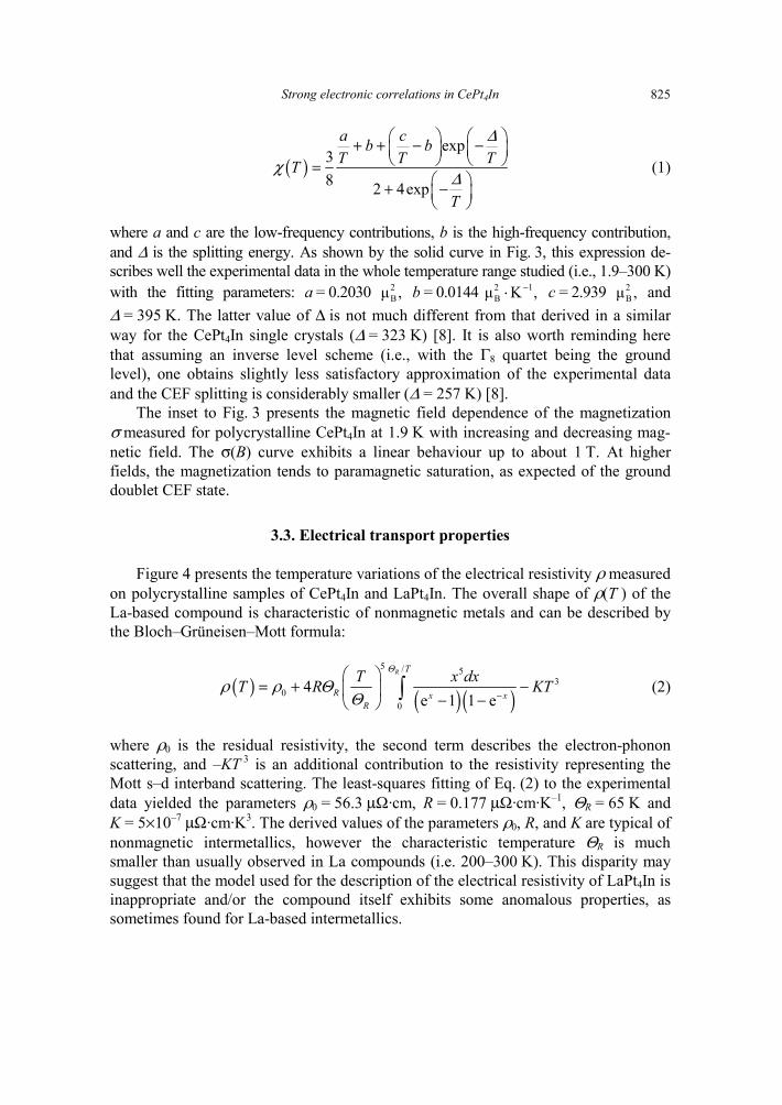
Strong electronic correlations in CePt4In 825
( )exp
38 2 4exp
a cb bT T TT
T
Δ
χΔ
⎛ ⎞ ⎛ ⎞+ + − −⎜ ⎟ ⎜ ⎟⎝ ⎠ ⎝ ⎠=
⎛ ⎞+ −⎜ ⎟⎝ ⎠
(1)
where a and c are the low-frequency contributions, b is the high-frequency contribution, and Δ is the splitting energy. As shown by the solid curve in Fig. 3, this expression de-scribes well the experimental data in the whole temperature range studied (i.e., 1.9–300 K) with the fitting parameters: a = 0.2030 2
Bμ , b = 0.0144 2 1Bμ K ,−⋅ c = 2.939 2
Bμ , and Δ = 395 K. The latter value of Δ is not much different from that derived in a similar way for the CePt4In single crystals (Δ = 323 K) [8]. It is also worth reminding here that assuming an inverse level scheme (i.e., with the Γ8 quartet being the ground level), one obtains slightly less satisfactory approximation of the experimental data and the CEF splitting is considerably smaller (Δ = 257 K) [8].
The inset to Fig. 3 presents the magnetic field dependence of the magnetization σ measured for polycrystalline CePt4In at 1.9 K with increasing and decreasing mag-netic field. The σ(B) curve exhibits a linear behaviour up to about 1 T. At higher fields, the magnetization tends to paramagnetic saturation, as expected of the ground doublet CEF state.
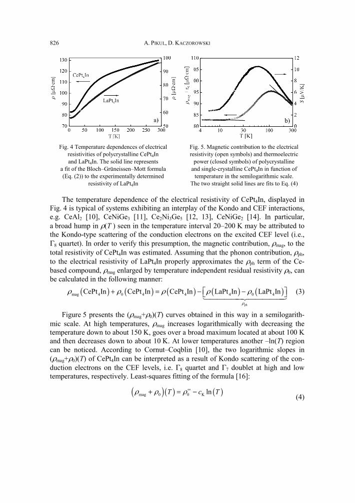
3.3. Electrical transport properties
Figure 4 presents the temperature variations of the electrical resistivity ρ measured on polycrystalline samples of CePt4In and LaPt4In. The overall shape of ρ(T ) of the La-based compound is characteristic of nonmagnetic metals and can be described by the Bloch–Grüneisen–Mott formula:
( ) ( )( )
5 / 53
00
4e 1 1 e
R T
R x xR
T x dxT R KTΘ
ρ ρ ΘΘ −
⎛ ⎞= + −⎜ ⎟
− −⎝ ⎠∫ (2)
where ρ0 is the residual resistivity, the second term describes the electron-phonon scattering, and –KT 3 is an additional contribution to the resistivity representing the Mott s–d interband scattering. The least-squares fitting of Eq. (2) to the experimental data yielded the parameters ρ0 = 56.3 μΩ·cm, R = 0.177 μΩ·cm·K–1, ΘR = 65 K and K = 5×10⁻⁷ μΩ·cm·K3. The derived values of the parameters ρ0, R, and K are typical of nonmagnetic intermetallics, however the characteristic temperature ΘR is much smaller than usually observed in La compounds (i.e. 200–300 K). This disparity may suggest that the model used for the description of the electrical resistivity of LaPt4In is inappropriate and/or the compound itself exhibits some anomalous properties, as sometimes found for La-based intermetallics.
A. PIKUL, D. KACZOROWSKI 826
Fig. 4 Temperature dependences of electrical
resistivities of polycrystalline CePt4In and LaPt4In. The solid line represents
a fit of the Bloch–Grüneissen–Mott formula (Eq. (2)) to the experimentally determined
resistivity of LaPt4In
Fig. 5. Magnetic contribution to the electrical resistivity (open symbols) and thermoelectric
power (closed symbols) of polycrystalline and single-crystalline CePt4In in function of
temperature in the semilogarithmic scale. The two straight solid lines are fits to Eq. (4)
The temperature dependence of the electrical resistivity of CePt4In, displayed in Fig. 4 is typical of systems exhibiting an interplay of the Kondo and CEF interactions, e.g. CeAl2 [10], CeNiGe3 [11], Ce2Ni3Ge5 [12, 13], CeNiGe2 [14]. In particular, a broad hump in ρ(T ) seen in the temperature interval 20–200 K may be attributed to the Kondo-type scattering of the conduction electrons on the excited CEF level (i.e., Γ8 quartet). In order to verify this presumption, the magnetic contribution, ρmag, to the total resistivity of CePt4In was estimated. Assuming that the phonon contribution, ρph, to the electrical resistivity of LaPt4In properly approximates the ρph term of the Ce-based compound, ρmag enlarged by temperature independent residual resistivity ρ0, can be calculated in the following manner:
( ) ( ) ( ) ( ) ( )ph
mag 4 0 4 4 4 0 4CePt In CePt In CePt In LaPt In LaPt Inρ
ρ ρ ρ ρ ρ⎡ ⎤+ = − −⎣ ⎦ (3)
Figure 5 presents the (ρmag+ρ0)(T) curves obtained in this way in a semilogarith-mic scale. At high temperatures, ρmag increases logarithmically with decreasing the temperature down to about 150 K, goes over a broad maximum located at about 100 K and then decreases down to about 10 K. At lower temperatures another –ln(T) region can be noticed. According to Cornut–Coqblin [10], the two logarithmic slopes in (ρmag+ρ0)(T) of CePt4In can be interpreted as a result of Kondo scattering of the con-duction electrons on the CEF levels, i.e. Γ8 quartet and Γ7 doublet at high and low temperatures, respectively. Least-squares fitting of the formula [16]:
( )( ) ( )mag 0 0 K lnT c Tρ ρ ρ ∞+ = − (4)
Strong electronic correlations in CePt4In 827
to the experimental data, yielded the parameters ρ0∞ = 139 and 83 μΩ·cm, and cK = 8.7
and 0.1 for the high- and low-temperature regions, respectively. Consequently, the CEF splitting Δ can be roughly estimated as being of the order of 100–150 K.
The temperature dependence of the Seebeck coefficient measured for single-crystalline CePt4In is plotted in Fig. 5 in a semilogarithmic scale. As reported in Ref. [8], the broad maximum, well visible at Tmax ≈ 60–70 K, is characteristic of dense Kondo systems and allows one to estimate the CEF splitting to be Δ = 3Tmax ≈ 180–210 K [15].
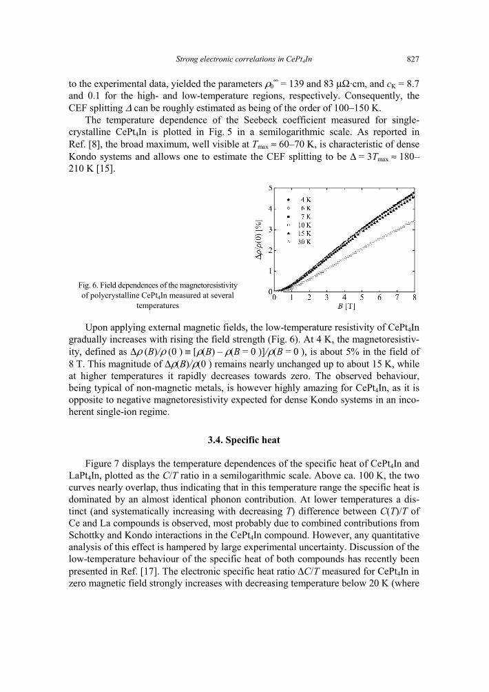
Fig. 6. Field dependences of the magnetoresistivity of polycrystalline CePt4In measured at several
temperatures
Upon applying external magnetic fields, the low-temperature resistivity of CePt4In gradually increases with rising the field strength (Fig. 6). At 4 K, the magnetoresistiv-ity, defined as Δρ (B)/ρ (0 ) ≡ [ρ(B) – ρ(B = 0 )]/ρ(B = 0 ), is about 5% in the field of 8 T. This magnitude of Δρ(B)/ρ(0 ) remains nearly unchanged up to about 15 K, while at higher temperatures it rapidly decreases towards zero. The observed behaviour, being typical of non-magnetic metals, is however highly amazing for CePt4In, as it is opposite to negative magnetoresistivity expected for dense Kondo systems in an inco-herent single-ion regime.
3.4. Specific heat
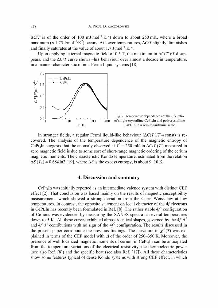
Figure 7 displays the temperature dependences of the specific heat of CePt4In and LaPt4In, plotted as the C/T ratio in a semilogarithmic scale. Above ca. 100 K, the two curves nearly overlap, thus indicating that in this temperature range the specific heat is dominated by an almost identical phonon contribution. At lower temperatures a dis-tinct (and systematically increasing with decreasing T) difference between C(T)/T of Ce and La compounds is observed, most probably due to combined contributions from Schottky and Kondo interactions in the CePt4In compound. However, any quantitative analysis of this effect is hampered by large experimental uncertainty. Discussion of the low-temperature behaviour of the specific heat of both compounds has recently been presented in Ref. [17]. The electronic specific heat ratio ΔC/T measured for CePt4In in zero magnetic field strongly increases with decreasing temperature below 20 K (where
A. PIKUL, D. KACZOROWSKI 828
ΔC/T is of the order of 100 mJ·mol−1·K–2) down to about 250 mK, where a broad maximum (≈ 1.75 J·mol−1·K2) occurs. At lower temperatures, ΔC/T slightly diminishes and finally saturates at the value of about 1.7 J·mol−1·K–2.
Upon applying external magnetic field of 0.5 T, the maximum in ΔC(T )/T disap-pears, and the ΔC/T curve shows –lnT behaviour over almost a decade in temperature, in a manner characteristic of non-Fermi liquid systems [18].
Fig. 7. Temperature dependences of the C/T ratio of single-crystalline CePt4In and polycrystalline
LaPt4In in a semilogarithmic scale
In stronger fields, a regular Fermi liquid-like behaviour (ΔC(T )/T ≈ const) is re-covered. The analysis of the temperature dependence of the magnetic entropy of CePt4In suggests that the anomaly observed at T* = 250 mK in ΔC/T (T ) measured in zero magnetic field is due to some sort of short-range magnetic ordering of the cerium magnetic moments. The characteristic Kondo temperature, estimated from the relation ΔS (TK) ≈ 0.68Rln2 [19], where ΔS is the excess entropy, is about 9–10 K.
4. Discussion and summary
CePt4In was initially reported as an intermediate valence system with distinct CEF effect [2]. That conclusion was based mainly on the results of magnetic susceptibility measurements which showed a strong deviation from the Curie–Weiss law at low temperatures. In contrast, the opposite statement on local character of the 4f electrons in CePt4In has recently been formulated in Ref. [8]. The rather stable 4f 1 configuration of Ce ions was evidenced by measuring the XANES spectra at several temperatures down to 5 K . All these curves exhibited almost identical shapes, governed by the 4f 1d 0 and 4f 1d 1 contributions with no sign of the 4f 0 configuration. The results discussed in the present paper corroborate the previous findings. The curvature in χ−1(T) was ex-plained in terms of the CEF model with Δ of the order of 250–350 K, Moreover, the presence of well localized magnetic moments of cerium in CePt4In can be anticipated from the temperature variations of the electrical resistivity, the thermoelectric power (see also Ref. [8]) and the specific heat (see also Ref. [17]). All these characteristics show some features typical of dense Kondo systems with strong CEF effect, in which
Strong electronic correlations in CePt4In 829
TK << Δ. In particular, the ultra-low temperature specific heat data revealed a short range magnetic ordering of the Kondo-screened magnetic moments at the temperature of 250 mK, consistent with the presence of well localized magnetic moments [17].
Most surprisingly, the results of magnetoresistivity measurements, performed on polycrystalline CePt4In, seem to contradict the Kondo scenario with TK of the order of 10 K (as derived from the entropy analysis). The values of the magnetoresistivity are positive in the whole temperature range studied, as expected of simple metals rather than of dense Kondo systems above the coherence temperature. Somewhat problem-atic are also different values of the CEF splitting derived from the analysis of the magnetic susceptibility (250–350 K) and the electrical resistivity (100–150 K), as well as rather large discrepancies (9–33 K) in values of the Kondo temperature estimated from the magnetic susceptibility and magnetic entropy data.
Thus CePt4In seems to be a dense Kondo system with localized magnetic mo-ments which experience strong CEF effect of cubic symmetry. The screened moments of the ground doublet probably exhibit some short-range magnetic ordering at very low temperatures. The character of that ordering as well as the characteristic energy scales of the system (TK and Δ) awaits verification by inelastic and elastic neutron scattering experiments, respectively.
Acknowledgements
This work was partially supported by the Polish Ministry of Science and Higher Education within a research project No. N202 116 32/3270. APP acknowledges support from the Alexander von Humboldt Foundation.
References
[1] DONIACH S., Valence Instabilities and Related Narrow Band Phenomena, Plenum Press, New York, 1977. [2] MALIK S.K., ADROJA D.T., SLASKI M., DUNLAP B.D., UMEZAWA A., Phys. Rev. B, 40 (1989), R9378. [3] HWANG J.S., LIN K., TIEN C., Rev. Sci. Instr., 68 (1997), 94. [4] RODRIGUEZ-CARVAJAL J., Physica B, 192 (1992), 55. [5] ADROJA D.T., MALIK S.K., PADALIA B.D., VIJAYARAGHAVAN R., Solid State Commun., 71 (1989), 649. [6] MALIK S.K., VIJAYARAGHAVAN R., ADROJA D.T., PADALIA B.D., EDELSTEIN A.S., J. Magn. Magn.
Mater., 92 (1990), 80. [7] OSAMURA K., MURAKAMI Y., J. Less-Com. Met., 60 (1978), 311. [8] PIKUL A.P., KACZOROWSKI D., BUKOWSKI Z., GOFRYK K., BURKHARDT U., GRIN YU., STEGLICH F.,
Phys. Rev. B, 73 (2006), 092406. [9] HEWSON A.C., The Kondo Problem to Heavy Fermions, Cambridge Univ. Press, Cambridge, 1997.
[10] CORNUT D., COQBLIN B., Phys. Rev. B, 5 (1972), 4541. [11] PIKUL A., KACZOROWSKI D., PLACKOWSKI T., CZOPNIK A., MICHOR H., BAUER E., HILSCHER G.,
ROGL P., GRIN YU., Phys. Rev. B, 67 (2003), 224417. [12] HOSSAIN Z., HAMASHIMA S., UMEO K., TAKABATAKE T., GEIBEL C., STEGLICH F., Phys. Rev. B,
62 (2000), 8950. [13] PIKUL A.P., KACZOROWSKI D., ROGL P., GRIN YU., Phys. Stat. Sol. B, 236 (2003), 364. [14] PIKUL A.P., KACZOROWSKI D., BUKOWSKI Z., PLACKOWSKI T., GOFRYK K., J. Phys.: Condens. Matter,
16 (2004), 6119.

A. PIKUL, D. KACZOROWSKI 830
[15] ZLATIČ V., HORVATIČ B., MILAT I., COQBLIN B., CZYCHOLL G., GRENZEBACH C., Phys. Rev. B, 68 (2003), 104432.
[16] KACZOROWSKI D., ROGL P., HIEBL K., Phys. Rev. B, 54 (1996), 9891. [17] PIKUL A.P., KACZOROWSKI D., BUKOWSKI Z, STEGLICH F., Physica B, 403 (2008), 842. [18] STEWART G.R., Rev. Mod. Phys., 73 (2001), 797. [19] DESGRANGES H.U., SCHOTTE K.D., Phys. Lett., 91A (1982), 240.
Received 7 May 2007 Revised 12 September 2007
Materials Science-Poland, Vol. 26, No. 4, 2008
NiFe/Au/Co/Au layered films Magnetic and transport properties
M. URBANIAK*
Institute of Molecular Physics, Polish Academy of Sciences, ul. M. Smoluchowskiego 17, 60-179 Poznań, Poland
Magnetic and magnetoresistive properties of [Ni80Fe20(tNiFe)/Au(tAu)/Co(tCo)/Au(tAu)]N multilayers characterized by the in-plane magnetic anisotropy of NiFe layers and the perpendicular anisotropy of Co layers have been described for a range of sublayer thicknesses and various numbers of repetitions N. It has been shown that the magnetic stray fields originating from the domain structure of Co layers, and calculated from the theory of Draaisma can qualitatively explain the measured R(H ) dependence in the field range corresponding to the magnetization reversal of Co layers. The investigated MLs are resistant to low temperature annealings. It has also been shown that the magnetic properties of MLs can be addi-tionally tailored by inserting thin Co layers on the NiFe/Au interfaces modifying the effective anisotropy of NiFe layers.
Key words: giant magnetoresistance; magnetic domains; perpendicular anisotropy
1. Introduction
The giant magnetoresistance (GMR) effect, i.e., the dependence of resistance of a magnetic system on the relative angle between magnetic moments of neighbouring layers or grains has been intensively investigated for almost two decades [1]. In our previous works [2–4] we have shown that GMR in NiFe/Au/Co/Au systems in which magnetic anisotropy alternates between in-plane and perpendicular orientation are potentially interesting from the application point of view as they exhibit a linear de-pendence of resistance (R) on the perpendicularly applied magnetic field (H). The perpendicular anisotropy of Co layers results from the influence of Au/Co interfaces. In this paper, we demonstrate that the most important features of the observed R(H ) dependences can be explained within the theory of Draaisma and de Jonge [5] al-though this theory describes multilayers (MLs) with purely perpendicular anisotropy.
__________
*E-mail: [email protected]
M. URBANIAK 832
We also analyze how the modifications of the structure change the magnetoresistance characteristics of MLs.
2. Experimental
The [Ni80Fe20(tNiFe)/Au(tAu)/Co(tCo)/Au(tAu)]N MLs with tNiFe = 2 nm, tAu = 1.5–3 nm, tCo = 0.6–1.2 nm and N = 1–15 were deposited in Ar atmosphere using UHV magne-tron sputtering. The films were deposited directly onto Si(100) substrates with native oxide. The sputtering rates were 0.06, 0.05, and 0.045 nm·s–1, for Au, NiFe and Co, respectively. The microstructure was investigated using X-ray diffraction with CuKα radiation. The magnetization reversal processes were studied at ambient temperature with a vibrating sample magnetometer (VSM). Current in-plane magnetoresistance (MR) was measured in a four-point configuration. Magnetic fields up to 1600 kA·m–1 (2 T), applied in-plane and perpendicularly, were used. The MR(H ) dependence was calculated relative to the resistance at 1600 kA·m–1 and the maximum value deter-mined from MR(H ) is called magnetoresistance (MR) amplitude. Some samples were cumulatively annealed in gas flow thermostat in dry N2 at temperatures tanneal up to 263 °C. Each annealing lasted 1 h.
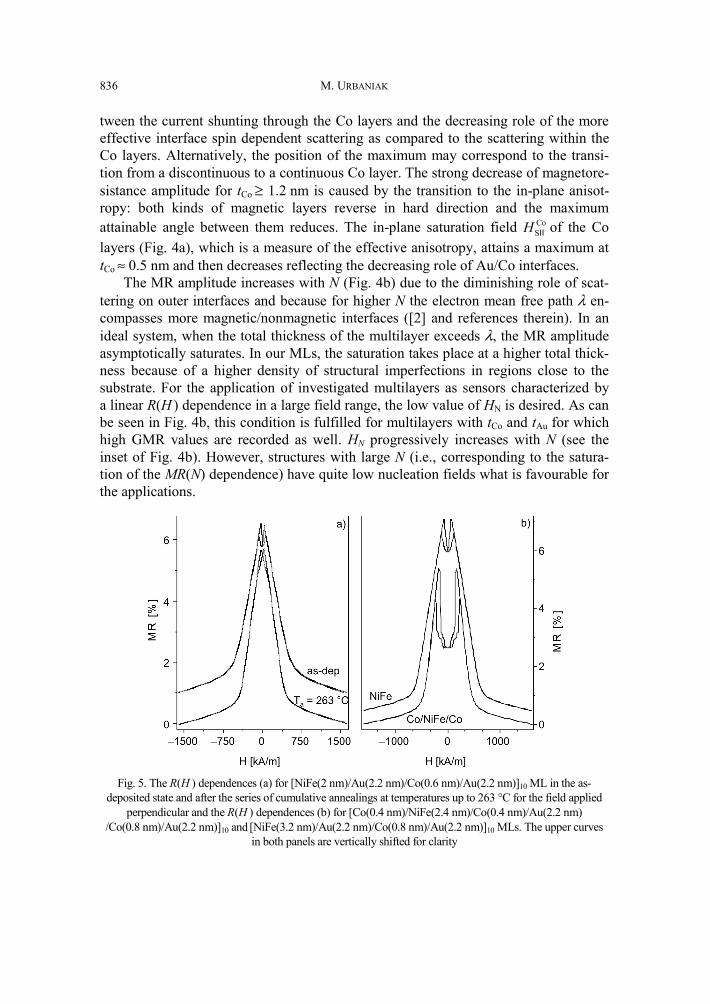
3. Results and discussion
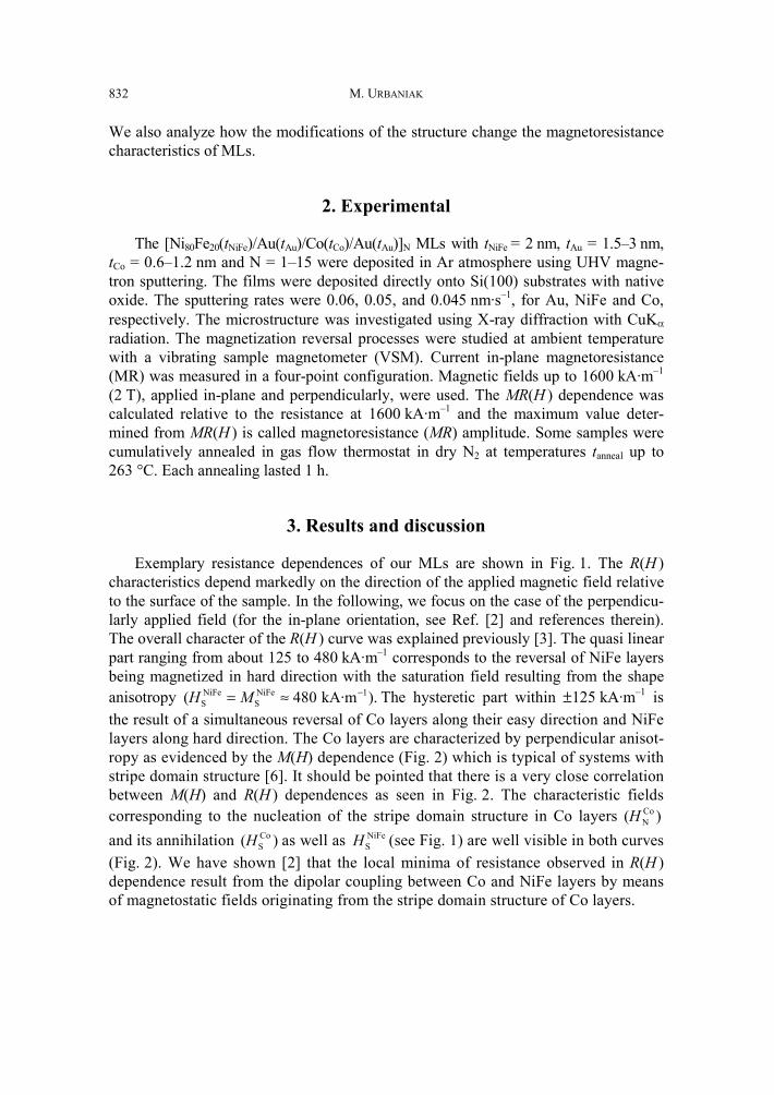
Exemplary resistance dependences of our MLs are shown in Fig. 1. The R(H ) characteristics depend markedly on the direction of the applied magnetic field relative to the surface of the sample. In the following, we focus on the case of the perpendicu-larly applied field (for the in-plane orientation, see Ref. [2] and references therein). The overall character of the R(H ) curve was explained previously [3]. The quasi linear part ranging from about 125 to 480 kA·m–1 corresponds to the reversal of NiFe layers being magnetized in hard direction with the saturation field resulting from the shape anisotropy NiFe NiFe 1
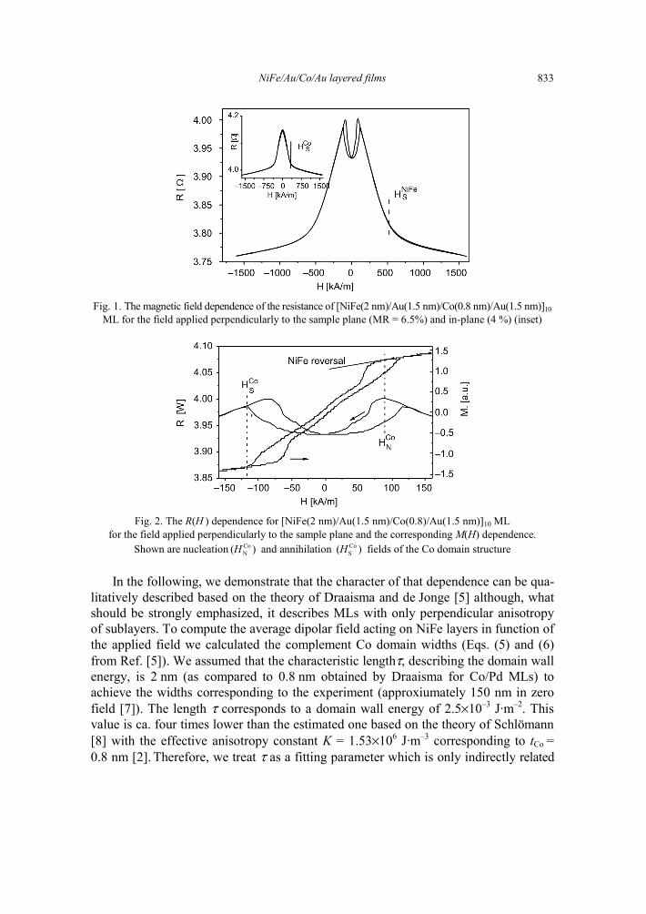
S S( 480 kA·m ).H M −= ≈ The hysteretic part within ±125 kA·m–1 is the result of a simultaneous reversal of Co layers along their easy direction and NiFe layers along hard direction. The Co layers are characterized by perpendicular anisot-ropy as evidenced by the M(H) dependence (Fig. 2) which is typical of systems with stripe domain structure [6]. It should be pointed that there is a very close correlation between M(H) and R(H ) dependences as seen in Fig. 2. The characteristic fields corresponding to the nucleation of the stripe domain structure in Co layers Co
N( )H and its annihilation Co
S( )H as well as NiFeSH (see Fig. 1) are well visible in both curves
(Fig. 2). We have shown [2] that the local minima of resistance observed in R(H ) dependence result from the dipolar coupling between Co and NiFe layers by means of magnetostatic fields originating from the stripe domain structure of Co layers.
NiFe/Au/Co/Au layered films 833
Fig. 1. The magnetic field dependence of the resistance of [NiFe(2 nm)/Au(1.5 nm)/Co(0.8 nm)/Au(1.5 nm)]10 ML for the field applied perpendicularly to the sample plane (MR = 6.5%) and in-plane (4 %) (inset)
Fig. 2. The R(H ) dependence for [NiFe(2 nm)/Au(1.5 nm)/Co(0.8)/Au(1.5 nm)]10 ML
for the field applied perpendicularly to the sample plane and the corresponding M(H) dependence. Shown are nucleation Co
N( )H and annihilation CoS( )H fields of the Co domain structure
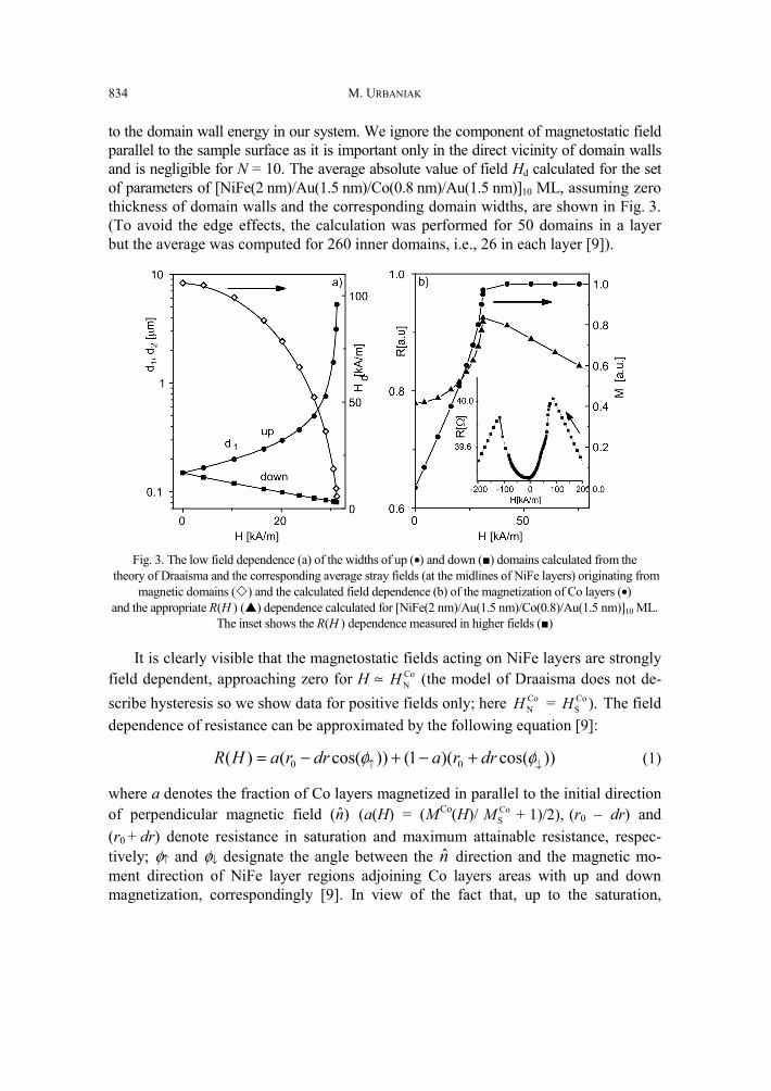
In the following, we demonstrate that the character of that dependence can be qua-litatively described based on the theory of Draaisma and de Jonge [5] although, what should be strongly emphasized, it describes MLs with only perpendicular anisotropy of sublayers. To compute the average dipolar field acting on NiFe layers in function of the applied field we calculated the complement Co domain widths (Eqs. (5) and (6) from Ref. [5]). We assumed that the characteristic lengthτ, describing the domain wall energy, is 2 nm (as compared to 0.8 nm obtained by Draaisma for Co/Pd MLs) to achieve the widths corresponding to the experiment (approxiumately 150 nm in zero field [7]). The length τ corresponds to a domain wall energy of 2.5×10⁻³ J·m–2. This value is ca. four times lower than the estimated one based on the theory of Schlömann [8] with the effective anisotropy constant K = 1.53×10⁶ J·m–3 corresponding to tCo = 0.8 nm [2]. Therefore, we treat τ as a fitting parameter which is only indirectly related
M. URBANIAK 834
to the domain wall energy in our system. We ignore the component of magnetostatic field parallel to the sample surface as it is important only in the direct vicinity of domain walls and is negligible for N = 10. The average absolute value of field Hd calculated for the set of parameters of [NiFe(2 nm)/Au(1.5 nm)/Co(0.8 nm)/Au(1.5 nm)]10 ML, assuming zero thickness of domain walls and the corresponding domain widths, are shown in Fig. 3. (To avoid the edge effects, the calculation was performed for 50 domains in a layer but the average was computed for 260 inner domains, i.e., 26 in each layer [9]).
Fig. 3. The low field dependence (a) of the widths of up (•) and down () domains calculated from the theory of Draaisma and the corresponding average stray fields (at the midlines of NiFe layers) originating from
magnetic domains ( ) and the calculated field dependence (b) of the magnetization of Co layers (•) and the appropriate R(H ) ( ) dependence calculated for [NiFe(2 nm)/Au(1.5 nm)/Co(0.8)/Au(1.5 nm)]10 ML.
The inset shows the R(H ) dependence measured in higher fields ()
It is clearly visible that the magnetostatic fields acting on NiFe layers are strongly field dependent, approaching zero for H ≈ Co
NH (the model of Draaisma does not de-scribe hysteresis so we show data for positive fields only; here Co
NH = CoS ).H The field
dependence of resistance can be approximated by the following equation [9]:
))cos()(1())cos(()( 00 ↓↑ +−+−= φφ drradrraHR (1)
where a denotes the fraction of Co layers magnetized in parallel to the initial direction of perpendicular magnetic field ˆ( )n (a(H) = (MCo(H)/ Co
S + 1)/2),M (r0 – dr) and (r0 + dr) denote resistance in saturation and maximum attainable resistance, respec-tively; φ↑ and φ↓ designate the angle between the n direction and the magnetic mo-ment direction of NiFe layer regions adjoining Co layers areas with up and down magnetization, correspondingly [9]. In view of the fact that, up to the saturation,
NiFe/Au/Co/Au layered films 835
cos(φ↑) and cos(φ↓) depend linearly on the effective field (cos(φ↓) = (H+Hd)/MSNiFe),
Eq. (1) can be rewritten as:
Co
0 NiFe CoS S
( )( ) [ ( )]ddr M HR H r H H H
M M= − + (2)
The calculated R(H ) dependence is shown in Fig. 3 (b) together with the corre-sponding measured one (inset). It is clearly visible that the overall character of the changes is relatively well described. The maximum resistance change attributed to the influence of domain fields NiFe
S( / )dH dr M is about 0.22dr in the model dependence and 0.44dr in the experimental one. The calculated and measured saturation fields of Co layers differ by some 60%. This is caused by the presence of stray fields originating from NiFe layers which were not present in the system analyzed by Draaisma and de Jonge. To adequately describe the R(H ) dependence one must utilize a dedicated theory which at present is not available in the literature. Nevertheless, the presented model confirms that the measured resistance characteristics of NiFe/Au/Co MLs have their origin in the dipolar fields of Co layers.
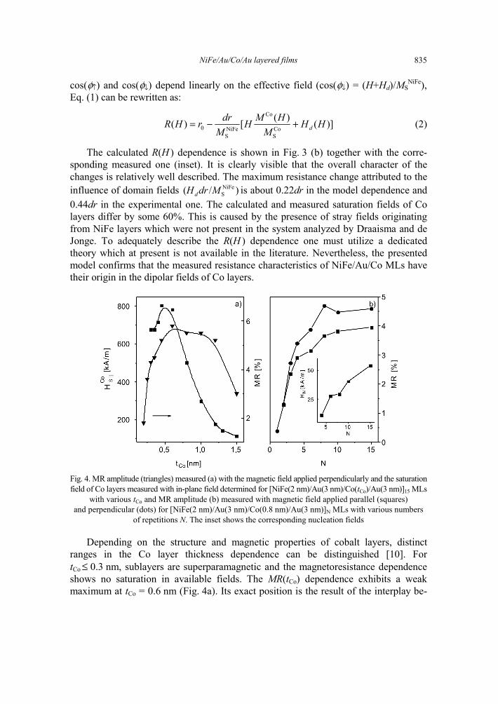
Fig. 4. MR amplitude (triangles) measured (a) with the magnetic field applied perpendicularly and the saturation field of Co layers measured with in-plane field determined for [NiFe(2 nm)/Au(3 nm)/Co(tCo)/Au(3 nm)]15 MLs
with various tCo and MR amplitude (b) measured with magnetic field applied parallel (squares) and perpendicular (dots) for [NiFe(2 nm)/Au(3 nm)/Co(0.8 nm)/Au(3 nm)]N MLs with various numbers
of repetitions N. The inset shows the corresponding nucleation fields
Depending on the structure and magnetic properties of cobalt layers, distinct ranges in the Co layer thickness dependence can be distinguished [10]. For tCo ≤ 0.3 nm, sublayers are superparamagnetic and the magnetoresistance dependence shows no saturation in available fields. The MR(tCo) dependence exhibits a weak maximum at tCo = 0.6 nm (Fig. 4a). Its exact position is the result of the interplay be-
M. URBANIAK 836
tween the current shunting through the Co layers and the decreasing role of the more effective interface spin dependent scattering as compared to the scattering within the Co layers. Alternatively, the position of the maximum may correspond to the transi-tion from a discontinuous to a continuous Co layer. The strong decrease of magnetore-sistance amplitude for tCo ≥ 1.2 nm is caused by the transition to the in-plane anisot-ropy: both kinds of magnetic layers reverse in hard direction and the maximum attainable angle between them reduces. The in-plane saturation field Co
SH II of the Co layers (Fig. 4a), which is a measure of the effective anisotropy, attains a maximum at tCo ≈ 0.5 nm and then decreases reflecting the decreasing role of Au/Co interfaces.
The MR amplitude increases with N (Fig. 4b) due to the diminishing role of scat-tering on outer interfaces and because for higher N the electron mean free path λ en-compasses more magnetic/nonmagnetic interfaces ([2] and references therein). In an ideal system, when the total thickness of the multilayer exceeds λ, the MR amplitude asymptotically saturates. In our MLs, the saturation takes place at a higher total thick-ness because of a higher density of structural imperfections in regions close to the substrate. For the application of investigated multilayers as sensors characterized by a linear R(H ) dependence in a large field range, the low value of HN is desired. As can be seen in Fig. 4b, this condition is fulfilled for multilayers with tCo and tAu for which high GMR values are recorded as well. HN progressively increases with N (see the inset of Fig. 4b). However, structures with large N (i.e., corresponding to the satura-tion of the MR(N) dependence) have quite low nucleation fields what is favourable for the applications.
Fig. 5. The R(H ) dependences (a) for [NiFe(2 nm)/Au(2.2 nm)/Co(0.6 nm)/Au(2.2 nm)]10 ML in the as-
deposited state and after the series of cumulative annealings at temperatures up to 263 °C for the field applied perpendicular and the R(H ) dependences (b) for [Co(0.4 nm)/NiFe(2.4 nm)/Co(0.4 nm)/Au(2.2 nm)
/Co(0.8 nm)/Au(2.2 nm)]10 and [NiFe(3.2 nm)/Au(2.2 nm)/Co(0.8 nm)/Au(2.2 nm)]10 MLs. The upper curves in both panels are vertically shifted for clarity
NiFe/Au/Co/Au layered films 837
Thermal stability is on of the important factors from the application point of view. Figure 5a shows that the MLs are quite resistant to annealing at tanneal up to 263 °C. The saturation field of R(H ) increases slightly but the magnetoresistance amplitude is preserved (detailed investigations of the thermal stability are shown in Ref. [11]).
The noticeable dependence of R(H ) curves on the properties of NiFe layers, namely their shape anisotropy, allows modifications of magnetoresistive characteris-tics by using composite layers instead of NiFe layers [3]. Figure 5b shows that replac-ing NiFe by Co/NiFe/Co leads to the diminishing of the saturation field of R(H ) de-pendence which is desirable for magnetic field sensing applications. One observes simultaneously that the change of resistance in a hysteretic range is much more pro-nounced. These changes in R(H ) can be explained remembering that thin Co layers adjoining to Au layers possess a perpendicular magnetic anisotropy [3]. Consequently, the composite layer, being strongly coupled by the direct exchange at NiFe/Co inter-faces, behaves like a single magnetic layer with diminished in-plane anisotropy. Ac-cordingly, the NiFe
SM in Eq. (2) should be replaced by CoNiFeCoSH which is lower in
value; this leads to larger changes of resistance under the influence of Hd.
4. Conclusions
The magnetostatic fields of Co layers computed within the theory of Draaisma and de Jonge qualitatively explain the behaviour of NiFe layers and the R(H ) characteris-tics. We showed that the use of the composite layers with in-plane anisotropy allow the modification of saturation fields of R(H ) dependence which is necessary from the application point of view.
Acknowledgements
This work was supported by the Polish State Committee for Scientific Research as a research project No. 3 T08A 03127.
References
[1] BAIBICH M. N., BROTO J.M., FERT A., NGUYEN VAN DAU, PETROFF F., ETIENNE P., CREUZET G., FRIEDERICH A., CHAZELAS J., Phys. Rev. Lett., 61 (1988), 2472.
[2] URBANIAK M., STOBIECKI F., SZYMAŃSKI B., EHRESMANN A., MAZIEWSKI A., TEKIELAK M., J. Appl. Phys., 101 (2007), 013905.
[3] STOBIECKI F., URBANIAK M., SZYMAŃSKI B., SCHMIDT M., LUCIŃSKI T., Phys. Stat. Sol. (b), 243 (2006), 210.
[4] SZYMAŃSKI B., STOBIECKI F., URBANIAK M., Phys. Stat. Sol. (b), 243 (2006), 235. [5] DRAAISMA H.J.G., DE JONGE W.J.G., J. Appl. Phys., 62 (1987), 3318. [6] HUBERT A., R. SCHÄFER R., Magnetic Domains: The Analysis of Magnetic Microstructures, Springer,
Berlin, 1998. [7] URBANIAK M., STOBIECKI F., ENGEL D., SZYMAŃSKI B., EHRESMANN A., KIM J.-B., Phys. Stat. Sol.
(c), 3 (2006), 57.

M. URBANIAK 838
[8] SCHLÖMANN E., J. Appl. Phys., 44 (1973), 1837. [9] URBANIAK M., STOBIECKI F., SZYMAŃSKI B., Phys. Stat. Sol. (a), 202 (2005), 2013.
[10] STOBIECKI F., SZYMAŃSKI B., LUCIŃSKI T., DUBOWIK J., URBANIAK M., RÖLL K., J. Magn. Magn. Mater., 282 (2004), 32.
[11] URBANIAK M., STOBIECKI F., SZYMAŃSKI B., J. Alloy. Comp., 454 (2008), 57.
Received 30 April 2007 Revised 10 May 2007
Materials Science-Poland, Vol. 26, No. 4, 2008
Micromagnetic properties of Co/Pt multilayers deposited on various buffer layers
M. CZAPKIEWICZ1*, J. KANAK1, T. STOBIECKI1, M. KACHEL1, M. ŻOŁĄDŹ1, I. SVEKLO2, A. MAZIEWSKI2, S. VAN DIJKEN3
1Department of Electronics, AGH University of Science and Technology, al. Mickiewicza 30, 30-059 Cracow, Poland
2Institute of Experimental Physics, University of Bialystok, Lipowa 41, 15-424 Bialystok, Poland 3VTT Micro and Nanoelectronics, P.O. Box 1000, FI-02044 VTT, Finland
A study on the buffer layer dependence of the film texture, surface roughness, and magnetization re-versal process in Co/Pt multilayers prepared by dc magnetron sputtering is presented. Oxidized Si(100) wafer was covered with four different buffers: (A) 10 nm Cu, (B) 5 nm Ta/10 nm Cu, (C) 5 nm Ta/10 nm Cu/5 nm Ta, and (D) 5 nm Ta/10 nm Cu/5 nm Ta/10 nm Cu. The growth of [2 nm Pt/0.5 nm Co]×5/2 nm Pt on top of these buffer layers results in a large variation in the fcc (111) Co/Pt texture and surface mor-phology. All films have the perpendicular magnetic anisotropy but magnetization reversal process, stud-ied by the magnetooptic Kerr effect (MOKE) and magnetic force spectroscopy (MFM), strongly depends on the buffer used. Observation of magnetic domains evolution under a MOKE microscope allows one to calculate from magnetization relaxation curves average dispersion of energy barriers of the thermal acti-vated magnetization switching process. The application of MFM in external magnetic field allows one to follow the dynamics of direct and indirect magnetization switching procesess up to submicrometer scale.
Key words: perpendicular anisotropy; magnetic domain; magnetization reversal
1. Introduction
Ferromagnetic multilayers with anisotropy perpendicular to the film plane are po-tentially interesting for application in high density magnetic recording. Systems with two magnetic states, “up” and “down”, with a good efficiency of the polar magneto-optical Kerr effect, are thus attractive for novel memory storage devices. Perpendicu-lar magnetic anisotropy (PMA) phenomena have been extensively investigated in mul-
__________
*Corresponding author, e-mail: [email protected]
M. CZAPKIEWICZ et al. 840
tilayer films prepared by a sequential deposition of ferromagnetic metals (Co, Fe, Ni) and nonferromagnetic noble metals (Pt, Au, Pd) [1–4]. More recently, perpendicular exchange bias effects have been studied in systems consisting of a PMA stack (for example [Pd/Co]n or [Pt/Co]n) and an antiferromagnetic layer (CoO [5, 6], FeMn [7, 8] or IrMn [9–11]). Many authors reported a variety of observed domain structures during magnetization reversal processes [12–14] occurring due to nucleation of a large number of small domains or by a smooth growth of a large cylindrical domains, or else by creep growth of irregular domains. A detailed study of magnetization rever-sal process by means of magnetooptic Kerr effect (MOKE) magnetometer, MOKE mi-croscopy or by magnetic force microscopy (MFM) revealed that a particular domain struc-ture and its dynamics related to the shape of the magnetization hysteresis loop depend strongly on the micromagnetic properties resulting from the layer interface structure.
In this paper, results of studies of structural, microstructural, magnetic and micro-magnetic properties are reported of PMA multilayer systems of [2 nm Pt/0.5 nm Co]×5/2 nm Pt deposited on various buffer layers with different degrees of fcc (111) Co/Pt texture. The model of energy barriers for thermally activated magnetization reversal process, successfully used elsewhere [15, 16], reveals a distinctive correlation between spatial dispersion of energy barriers and texture of used buffer layers.
2. Experimental
The [2 nm Pt/0.5 nm Co]×5/2 nm Pt multilayers were grown on four buffers: 10 nm Cu (A), 5 nm Ta/10 nm Cu (B), 5 nm Ta/10 nm Cu/5 nm Ta (C), and 5 nm Ta/10 nm Cu/5 nm Ta/10 nm Cu (D). Recently, it was shown that for a sample with Cu buffer (sample A), a small contribution of Cu (200) texture was observed in addition to (111) texture [17]. However, a pronounced (111) Cu texture appears when Ta is used as a seed layer on silicon oxide (sample B). The buffers C and D were used to change the texture degree by repetition of Ta/Cu bilayers in the system. The buffers and Co/Pt multilayers were deposited on Si(100) wafer with 500 nm thick SiO2 by dc magnetron sputtering at ambient temperature.
After deposition, roughness and morphology of the multilayer surfaces were ex-amined by AFM. The structure was characterized by X-ray diffraction (XRD) using θ–2θ scans, rocking curves (ω scans) and X-ray reflectivity [11]. SQUID measure-ments with the field parallel to the film plane were performed to saturate the magneti-zation in the film plane and determine effective anisotropy field HK. The effective anisotropy is given by the equation
eff 01 2 K SK H Mμ= (1)
beings a superposition of crystalline anisotropy of Co layers and surface anisotropy of the Co/Pt interface [18]. This large effective anisotropy energy is responsible for the perpendicular to the plane orientation of magnetization in a remanent state. Magneti-
Micromagnetic properties of Co/Pt multilayers deposited on buffer layers 841
zation reversal hysteresis loops with field perpendicular to the film plane were re-corded by means of the MOKE magnetometer [19] to verify the coercivity and hys-teresis loop squareness. The magnetooptical contrast of magnetic domains was ob-served by the MOKE microscopy [20] with the spatial resolution down to 1 μm. Thanks to a special system for real-time image processing, evolution of domain struc-ture was recorded and stored with the 25 frames per second rate. The thermally acti-vated magnetic reversal process was studied by recording the evolution of magnetic domains in a constant field perpendicular to the film plane. It is convenient to study relaxation of metastable state of magnetization in a constant negative magnetic field lower than the critical switching field [21]. Magnetization relaxation from a saturated state MS to –MS can be represented by the fractional magnetization B(t) not yet re-versed at a time t
( ) ( )2
S
S
M t MB tM+= (2)
Such a fractional area B can be derived from the image of MOKE contrast as the ratio of the white area (spins down) to the total area of the observed ferromagnetic sample. For the PMA thin films and multilayers magnetization reversal occurs usually by nucleation and growth of cylindrical domains. As was shown by Labrune et. al. [22], the Fatuzzo model [23] can be used to express the influence of competition be-tween the nucleation probability rate R and domain expansion velocity v on the shape of B(t) by a dimensionless parameter
c
vkr R
= (3)
where rc is the radius of the initial domain. The nucleation probability rate as well as the velocity of domain expansion depend exponentially on the activation energy bar-rier W
00 exp S B
B
W M HVR Rk Tμ⎛ ⎞−= −⎜ ⎟
⎝ ⎠ (4)
00 exp S B
B
W M HVv vk Tμ⎛ ⎞−= −⎜ ⎟
⎝ ⎠ (5)
The energy barrier decreases with the external magnetic field H proportionally to the Barkhausen volume VB, i.e. magnetization volume that reverses during a single activation event. Under the above assumptions, the relaxation of magnetization is given by the Fatuzzo formula:
( ) ( ) ( ) ( ) ( )( )22 1 1 1 2exp 2 1 0.5 e 1 0.5 1RtB t k Rt k Rt k k k Rt− − − − −⎛ ⎞= − − + + + − − − −⎜ ⎟⎝ ⎠
(6)
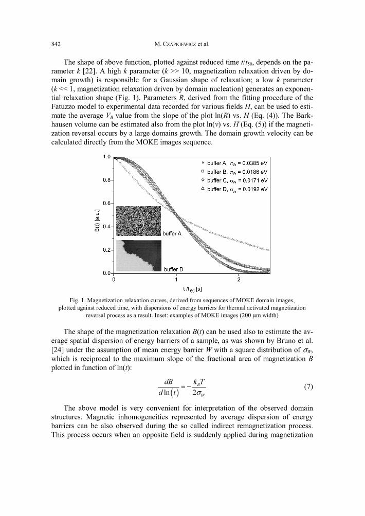
M. CZAPKIEWICZ et al. 842
The shape of above function, plotted against reduced time t/t50, depends on the pa-rameter k [22]. A high k parameter (k >> 10, magnetization relaxation driven by do-main growth) is responsible for a Gaussian shape of relaxation; a low k parameter (k << 1, magnetization relaxation driven by domain nucleation) generates an exponen-tial relaxation shape (Fig. 1). Parameters R, derived from the fitting procedure of the Fatuzzo model to experimental data recorded for various fields H, can be used to esti-mate the average VB value from the slope of the plot ln(R) vs. H (Eq. (4)). The Bark-hausen volume can be estimated also from the plot ln(v) vs. H (Eq. (5)) if the magneti-zation reversal occurs by a large domains growth. The domain growth velocity can be calculated directly from the MOKE images sequence.
Fig. 1. Magnetization relaxation curves, derived from sequences of MOKE domain images,
plotted against reduced time, with dispersions of energy barriers for thermal activated magnetization reversal process as a result. Inset: examples of MOKE images (200 μm width)
The shape of the magnetization relaxation B(t) can be used also to estimate the av-erage spatial dispersion of energy barriers of a sample, as was shown by Bruno et al. [24] under the assumption of mean energy barrier W with a square distribution of σW, which is reciprocal to the maximum slope of the fractional area of magnetization B plotted in function of ln(t):
( )ln 2B
W
dB k Td t σ
= − (7)
The above model is very convenient for interpretation of the observed domain structures. Magnetic inhomogeneities represented by average dispersion of energy barriers can be also observed during the so called indirect remagnetization process. This process occurs when an opposite field is suddenly applied during magnetization
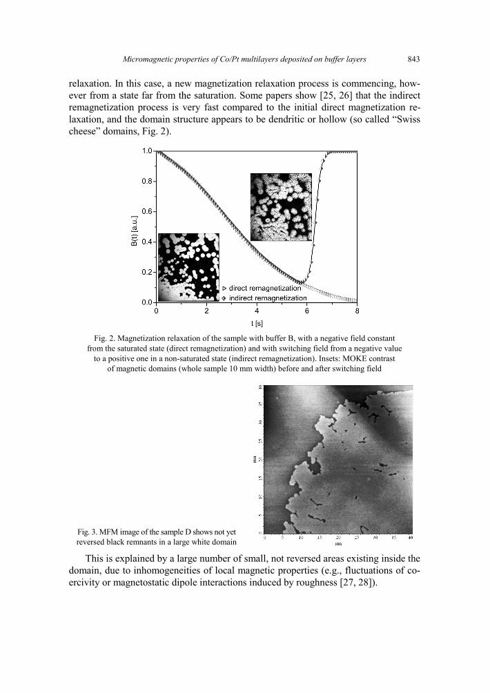
Micromagnetic properties of Co/Pt multilayers deposited on buffer layers 843
relaxation. In this case, a new magnetization relaxation process is commencing, how-ever from a state far from the saturation. Some papers show [25, 26] that the indirect remagnetization process is very fast compared to the initial direct magnetization re-laxation, and the domain structure appears to be dendritic or hollow (so called “Swiss cheese” domains, Fig. 2).
Fig. 2. Magnetization relaxation of the sample with buffer B, with a negative field constant
from the saturated state (direct remagnetization) and with switching field from a negative value to a positive one in a non-saturated state (indirect remagnetization). Insets: MOKE contrast
of magnetic domains (whole sample 10 mm width) before and after switching field
Fig. 3. MFM image of the sample D shows not yet reversed black remnants in a large white domain
This is explained by a large number of small, not reversed areas existing inside the domain, due to inhomogeneities of local magnetic properties (e.g., fluctuations of co-ercivity or magnetostatic dipole interactions induced by roughness [27, 28]).
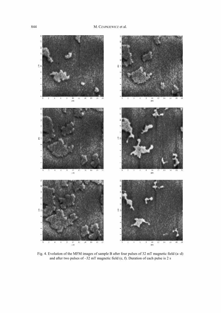
M844
Fig. 4. Evolution of the MFM images oand after two pulses of –32 mT
M. CZAPKIEWICZ et al.
of sample B after four pulses of 32 mT magnetic field (a–d) T magnetic field (e, f). Duration of each pulse is 2 s
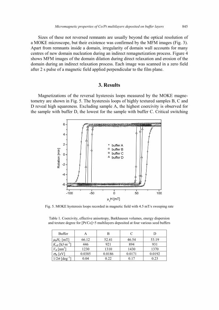
Micromagnetic properties of Co/Pt multilayers deposited on buffer layers 845
Sizes of these not reversed remnants are usually beyond the optical resolution of a MOKE microscope, but their existence was confirmed by the MFM images (Fig. 3). Apart from remnants inside a domain, irregularity of domain wall accounts for many centres of new domain nucleation during an indirect remagnetization process. Figure 4 shows MFM images of the domain dilation during direct relaxation and erosion of the domain during an indirect relaxation process. Each image was scanned in a zero field after 2 s pulse of a magnetic field applied perpendicular to the film plane.
3. Results
Magnetizations of the reversal hysteresis loops measured by the MOKE magne-tometry are shown in Fig. 5. The hysteresis loops of highly textured samples B, C and D reveal high squareness. Excluding sample A, the highest coercivity is observed for the sample with buffer D, the lowest for the sample with buffer C. Critical switching
Fig. 5. MOKE hysteresis loops recorded in magnetic field with 4.5 mT/s sweeping rate
Table 1. Coercivity, effective anisotropy, Barkhausen volumes, energy dispersion and texture degree for [Pt/Co]×5 multilayers deposited at four various seed buffers
Buffer A B C D μ0HC [mT] 66.12 52.41 46.54 53.19 Keff [kJ·m–3] 446 921 894 931 VB [nm3] 1230 1310 1430 1370 σW [eV] 0.0385 0.0186 0.0171 0.0192 1/2σ [deg–1] 0.04 0.22 0.17 0.23
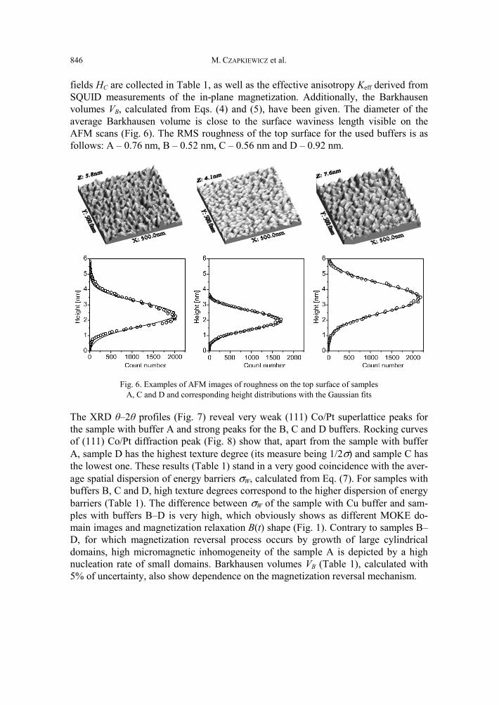
M846
fields HC are collected in Table 1, aSQUID measurements of the in-pvolumes VB, calculated from Eqs. average Barkhausen volume is cloAFM scans (Fig. 6). The RMS roufollows: A – 0.76 nm, B – 0.52 nm,
Fig. 6. Examples of AFM imA, C and D and correspond
The XRD θ–2θ profiles (Fig. 7) rethe sample with buffer A and strongof (111) Co/Pt diffraction peak (FiA, sample D has the highest texturethe lowest one. These results (Tableage spatial dispersion of energy barbuffers B, C and D, high texture debarriers (Table 1). The difference bples with buffers B–D is very highmain images and magnetization relaD, for which magnetization reversdomains, high micromagnetic inhonucleation rate of small domains. B5% of uncertainty, also show depen
M. CZAPKIEWICZ et al.
as well as the effective anisotropy Keff derived fromplane magnetization. Additionally, the Barkhausen(4) and (5), have been given. The diameter of those to the surface waviness length visible on th
ughness of the top surface for the used buffers is a, C – 0.56 nm and D – 0.92 nm.
mages of roughness on the top surface of samples ding height distributions with the Gaussian fits
eveal very weak (111) Co/Pt superlattice peaks fog peaks for the B, C and D buffers. Rocking curveig. 8) show that, apart from the sample with buffee degree (its measure being 1/2σ) and sample C hae 1) stand in a very good coincidence with the averrriers σW, calculated from Eq. (7). For samples withegrees correspond to the higher dispersion of energybetween σW of the sample with Cu buffer and samh, which obviously shows as different MOKE doaxation B(t) shape (Fig. 1). Contrary to samples B–sal process occurs by growth of large cylindricaomogeneity of the sample A is depicted by a highBarkhausen volumes VB (Table 1), calculated with
ndence on the magnetization reversal mechanism.
m n
he he as
or es er as r-h y
m-o-–al h h
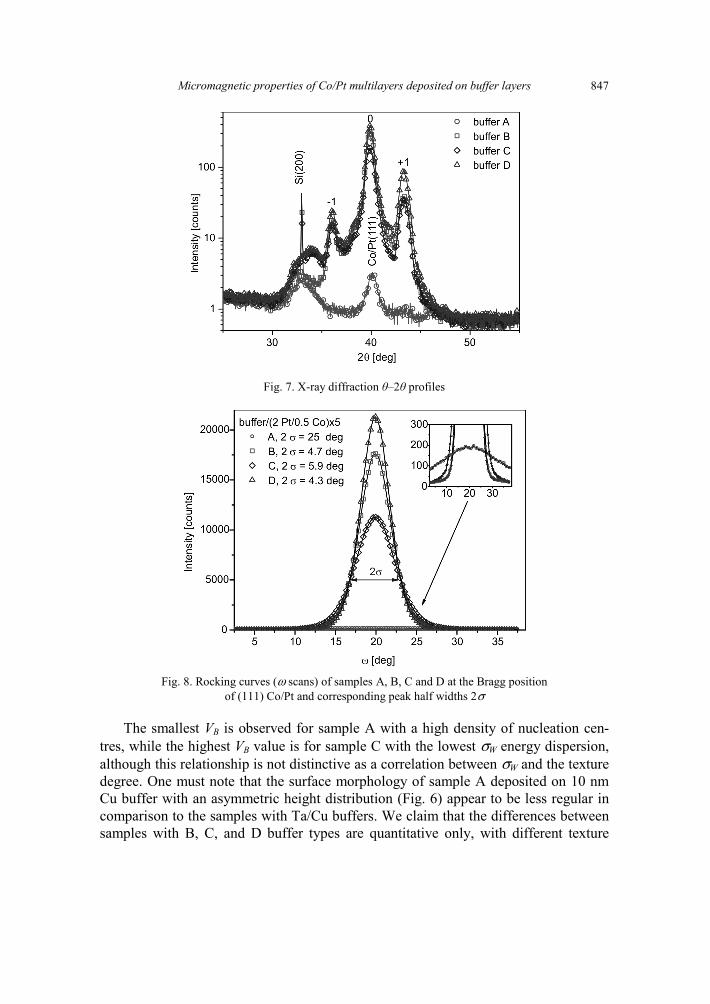
Micromagnetic properties of Co/Pt multilayers deposited on buffer layers 847
Fig. 7. X-ray diffraction θ–2θ profiles
Fig. 8. Rocking curves (ω scans) of samples A, B, C and D at the Bragg position of (111) Co/Pt and corresponding peak half widths 2σ
The smallest VB is observed for sample A with a high density of nucleation cen-tres, while the highest VB value is for sample C with the lowest σW energy dispersion, although this relationship is not distinctive as a correlation between σW and the texture degree. One must note that the surface morphology of sample A deposited on 10 nm Cu buffer with an asymmetric height distribution (Fig. 6) appear to be less regular in comparison to the samples with Ta/Cu buffers. We claim that the differences between samples with B, C, and D buffer types are quantitative only, with different texture
M. CZAPKIEWICZ et al. 848
degree but well defined superlattice structure. On the contrary, the growth of Cu buffer (sample A) produces poor quality of a superlattice structure. We claim that existence of both (200) and (111) Cu crystallographic orientations [17] is related to disorder of the buffer structure of single Cu layer.
4. Conclusions
Magnetic properties, especially the domain pattern and magnetization reversal process, strongly depend on structural properties of ferromagnetic multilayers deter-mined by growth on various textured buffers. High texture degree and Pt/Co interface waviness result in a higher inhomogeneity of micromagnetic properties and a non-uniform magnetization reversal process, with pinning centres, non-reversed remnants and increased coercivity. Such inhomogeneities give rise to irreversible remagnetiza-tion process. In the extreme case of high fluctuation of magnetic properties caused by improper growth of the seed buffer (for example 10 nm Cu on amorphous SiO2), the saturation field should be high enough to provide uniform magnetization and over-come energy barrier blocking reversal of local pinning centres.
Thermally activated magnetization relaxations are very sensitive to the spatial dis-persion of reversal energy barriers, thus analysis of the relaxation curves is a good tool to study quality of layers and multilayers with perpendicular magnetic anisotropy.
Acknowledgements
This work was supported by projects of Polish Ministry of Science and Higher Education and project of Research and Training Network (RTN) NANOMAG-LAB (No. 2004-003177).
References
[1] CARCIA P.F., MEINHOLDT A.D., SUNA A., Appl. Phys. Lett. 47, (1985) 178. [2] DEN BROEDER F.J.A., KUIPER D., VAN DE MOSSELAER A.P., HOVING W., Phys. Rev. Lett. 60, (1988)
2769. [3] CARCIA P.F., J. Appl. Phys 63, (1988) 5066. [4] JEONG J-R., KIM Y-S., SHIN S-C., J. Appl. Phys, 85, (1999) 5762. [5] MAAT S., TAKANO K., PARKIN S.S.P., FULLERTON E.E., Phys. Rev. Lett. 87, (2001) 087202. [6] HELLWIG O., MAAT S., KORTRIGHT J.B., FULLERTON E.E., Phys. Rev. B 65, (2002) 144418. [7] GARCIA F., CASALI G., AUFFRET S., RODMACQ B., DIENY B., J. Appl. Phys. 91, (2002) 6905. [8] SORT J., RODMACQ B., AUFFRET S., DIENY B., Appl. Phys Lett. 83, (2003) 1800. [9] VAN DIJKEN S., MORITZ J., COEY J.M.D., J. Appl. Phys. 97, (2005) 063907.
[10] SORT J., BALTZ V., GARCIA F., RODMACQ B., DIENY B., Phys. Rev B 71, (2005) 054411. [11] KANAK J., STOBIECKI T., VAN DIJKEN S., IEEE Trans. Mag., 44 (2008), 238. [12] ROMANENS F., PIZZINI S., YOKAICHIYA F., BONFIM M., PENNEC Y., CAMARERO J., VOGEL J., SORT J.,
GARCIA F., RODMAQ B., DIENY B., Phys. Rev. B 72, (2005) 134410. [13] CZAPKIEWICZ M., VAN DIJKEN S., STOBIECKI T., RAK R., ZOLADZ M., MIETNIOWSKI P., Phys. Stat.
Sol. (c) 3, (2006) 48.
Micromagnetic properties of Co/Pt multilayers deposited on buffer layers 849
[14] WIEBEL S., JAMET J.-P., VERNIER N., MOUGIN A., FERRÉ J., BALTZ V., RODMACQ B., DIENY B., J. Appl. Phys 100, (2006) 043912,.
[15] MALINOWSKI G., VAN DIJKEN S., CZAPKIEWICZ M., STOBIECKI T., Appl. Phys Lett. 90, (2007) 082501.
[16] CZAPKIEWICZ M., STOBIECKI T., VAN DIJKEN S., Phys. Rev. B, 77 (2008), 024416. [17] WISNIOWSKI P., STOBIECKI T., KANAK J., REISS G., BRÜCKL H., J. Appl. Phys. 100 (2006) 013906. [18] DAALDEROP G.H.O., KELLY P.J., SCHUURMANS M.F.H., Phys. Rev. B 42, (1990) 7270. [19] WRONA J., STOBIECKI T., RAK R., CZAPKIEWICZ M., STOBIECKI F., UBA L., KORECKI J., SLEZAK T.,
WILGOCKA-SLEZAK J., ROTS M., Phys. Stat. Sol. (a) 196, (2003) 161. [20] ZOLADZ M., KNAPPMANN S., OTTO M., RÖLL K., STOBIECKI T., Phys. Stat. Sol. (a) 189, (2002) 791. [21] POMMIER J., MEYER P., PÉNISSARD G., FERRÉ J., BRUNO P., RENARD D., Phys. Rev. Lett. 65, (1990)
2054. [22] LABRUNE M., ANDRIEU S., RIO F., BERNSTEIN P., J. Magn. Magn. Mater. 80, (1989) 211. [23] FATUZZO E., Phys.Rev. 127, (1962) 1999. [24] BRUNO P., BAYREUTHER G., BEAUVILLAIN P., CHAPPERT C., LUGERT G., RENARD D., RENARD J.P.,
SEIDEN J., J. Appl. Phys. 68, (1990) 5759. [25] FERRÉ J., GROLIER V., MEYER P., LEMERLE S., MAZIEWSKI A., STEFANOWICZ E., TARASENKO S.V.,
TARASENKO V.V., KISIELEWSKI M., RENARD D., Phys. Rev. B 55, (1997) 15092. [26] KISIELEWSKI M., MAZIEWSKI A., TEKIELAK M., FERRÉ J., LEMERLE S., MATHET V., CHAPPERT C.,
J. Magn. Magn. Mater, 260 (2003) 231–243. [27] Meneghini C., MARET M., PARASOTE V., CADEVILLE M.C., HAZEMANN J.L., CORTES R., COLONNA S.,
Eur. Phys. J. B 7, (1999) 347. [28] JANG H-J., CHOE S-B., SHIN S-C., J. Appl. Phys 93, (2003) 10143.
Received 30 April 2007 Revised 10 May 2007
Materials Science-Poland, Vol. 26, No. 4, 2008
Optical control and decoherence of spin qubits in quantum dots
P. MACHNIKOWSKI1*, A. GRODECKA1,2**, C. WEBER2***, A. KNORR2
1Institute of Physics, Wrocław University of Technology, 50-370 Wrocław, Poland 2Institut für Theoretische Physik, Technische Universität Berlin, 10623 Berlin, Germany
Various methods of all-optical spin control in semiconductor quantum dots are discussed, and differ-ent ways of rotating a single confined electron spin by optical coupling to a trion state are presented in the paper. A method for controlling the polarization of a confined exciton via a two-photon transition is also discussed. Finally, the effect of phonon-induced decoherence on the fidelity of these optical spin control protocols is analysed.
Key words: quantum computing; semiconductor; all-optical control; dephasing
1. Introduction
Single electron spins confined in semiconductor quantum dots (QDs) seem to be promising candidates for implementing quantum information processing schemes. The main advantage of these systems is their relatively long coherence time. Many control protocols for spins in QDs have been developed, mostly based on applying external voltages and exploiting exchange interactions.
It is, however, also possible to control spins by optical means. In quantum dots, this can be done by inducing charge dynamics dependent on the spin state of an elec-tron, which is possible due to the optical selection rules and Pauli exclusion principle. Such control methods lead to very short switching times, even on picosecond time scales. A few control protocols of this kind have been proposed [1–6]. Their common feature is the optical coupling of both spin states to a trion (charged exciton) state. This opens a quantum pathway between the two spin states via a Raman transition. In this way, optical coherent control of a spin in a QD becomes possible.
__________
*Corresponding author, e-mail: [email protected] **Current address: Computational Nanophotonics Group Theoretical Physics, University Paderborn,
Warburgerstr. 100, 33098 Paderborn, Germany. ***Current address: Mathematical Physics, Lund University, Box 118, 22100 Lund, Sweden.
P. MACHNIKOWSKI et al. 852
In this paper, these optical spin control schemes will be reviewed, mostly from a theoretical point of view. Schemes for rotating electron spins as well as methods for optical control of exciton polarization (by coupling to the biexciton state) will be dis-cussed. This review will be followed by an analysis of decoherence processes accom-panying the optical spin control schemes. The latter may result from the lattice re-sponse to the charge evolution necessary to perform the spin rotation [7] and from the finite lifetime of the trion excitation used in the optical control schemes. Another source of discrepancies from the desired spin rotation (errors of a single-qubit gate) is an imperfect adiabacity of the evolution. A possible optimization against these errors will be discussed.
2. Band structure and selection rules for interband transitions in III–V semiconductors
Quantum dots are semiconductor structures in which the carrier dynamics is re-stricted in all three dimensions to the length scales of several or a few tens of nanome-ters [8]. Since the effective mass of carriers is usually considerably lower than the free electron mass, this degree of confinement is sufficient for quantization of carrier ener-gies with electron inter-level spacing reaching 100 meV in self-assembled structures.
The valence band in III–V semiconductors is composed of p-type atomic orbitals (orbital angular momentum 1), yielding six quantum states (taking spin into account) for each quasimomentum k. Due to a considerable spin-orbit interaction, the orbital angular momentum and spin are not separate good quantum numbers and the valence band states of a bulk crystal must be classified by the total angular momentum and its projection on a selected axis. Thus, the valence band is composed of three subbands corresponding to two different representations of the total angular momentum J. Out of these, the two states with j = 1/2 form a subband which is split-off by the spin-orbit interaction. The other four states with j = 3/2 are degenerate in bulk at k = 0 but this degeneracy is lifted by size quantization and strain in a QD structure, with the heavy hole (hh) subband (angular momentum projection on the symmetry axis m = ±3/2) lying above the light hole (lh) subband (m = ±1/2) in all known structures.
The fundamental optical excitation of a QD consists in transferring optically an electron from the highest confined state in the valence band (thus leaving a hole) to the lowest confined state in the conduction band. The interacting electron–hole pair created in this way is referred to as exciton (lh exciton or hh exciton, depending on the kind of hole involved). Angular momentum selection rules restrict the transitions al-lowed for a given propagation direction and polarization of the light beam, as depicted in Fig. 1. For instance, according to the selection rules represented in Fig. 1b, a σ+, polarized laser beam can only create an exciton with total momentum +1, referred to as “σ+ exciton”, in accordance with the angular momentum conservation (removing an electron with the angular momentum m is equivalent to the creation of a hole with the
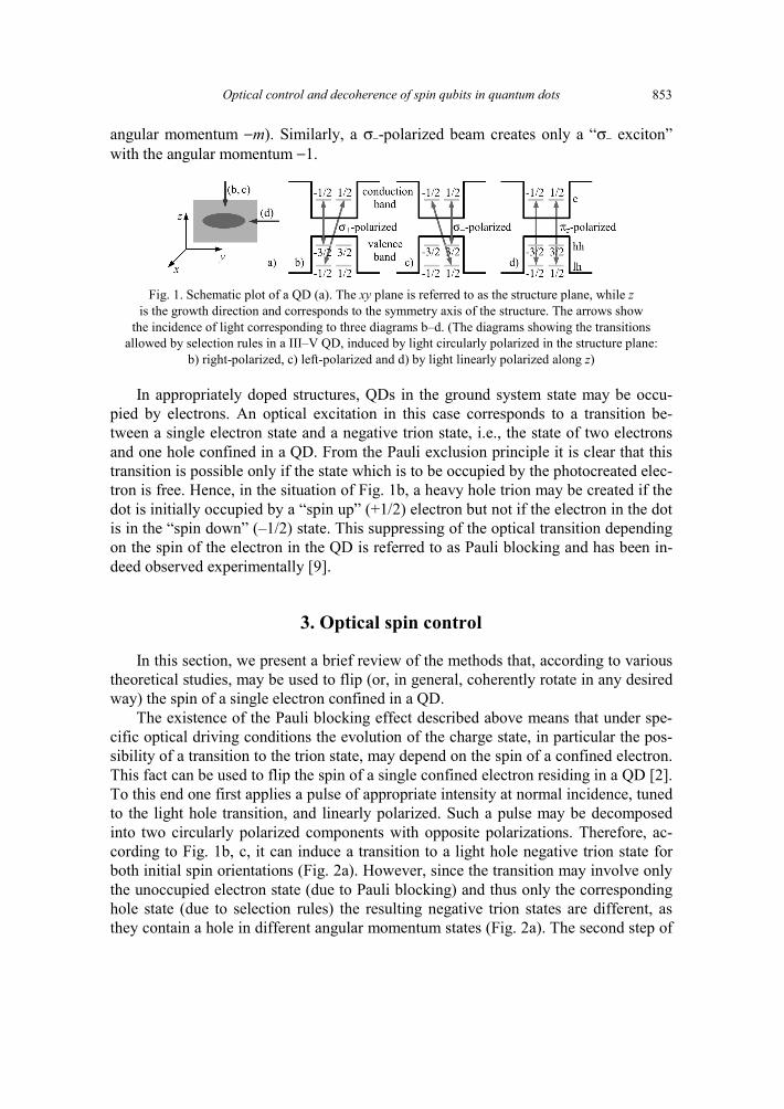
Optical control and decoherence of spin qubits in quantum dots 853
angular momentum −m). Similarly, a σ−-polarized beam creates only a “σ− exciton” with the angular momentum −1.
Fig. 1. Schematic plot of a QD (a). The xy plane is referred to as the structure plane, while z
is the growth direction and corresponds to the symmetry axis of the structure. The arrows show the incidence of light corresponding to three diagrams b–d. (The diagrams showing the transitions
allowed by selection rules in a III–V QD, induced by light circularly polarized in the structure plane: b) right-polarized, c) left-polarized and d) by light linearly polarized along z)
In appropriately doped structures, QDs in the ground system state may be occu-pied by electrons. An optical excitation in this case corresponds to a transition be-tween a single electron state and a negative trion state, i.e., the state of two electrons and one hole confined in a QD. From the Pauli exclusion principle it is clear that this transition is possible only if the state which is to be occupied by the photocreated elec-tron is free. Hence, in the situation of Fig. 1b, a heavy hole trion may be created if the dot is initially occupied by a “spin up” (+1/2) electron but not if the electron in the dot is in the “spin down” (–1/2) state. This suppressing of the optical transition depending on the spin of the electron in the QD is referred to as Pauli blocking and has been in-deed observed experimentally [9].
3. Optical spin control
In this section, we present a brief review of the methods that, according to various theoretical studies, may be used to flip (or, in general, coherently rotate in any desired way) the spin of a single electron confined in a QD.
The existence of the Pauli blocking effect described above means that under spe-cific optical driving conditions the evolution of the charge state, in particular the pos-sibility of a transition to the trion state, may depend on the spin of a confined electron. This fact can be used to flip the spin of a single confined electron residing in a QD [2]. To this end one first applies a pulse of appropriate intensity at normal incidence, tuned to the light hole transition, and linearly polarized. Such a pulse may be decomposed into two circularly polarized components with opposite polarizations. Therefore, ac-cording to Fig. 1b, c, it can induce a transition to a light hole negative trion state for both initial spin orientations (Fig. 2a). However, since the transition may involve only the unoccupied electron state (due to Pauli blocking) and thus only the corresponding hole state (due to selection rules) the resulting negative trion states are different, as they contain a hole in different angular momentum states (Fig. 2a). The second step of
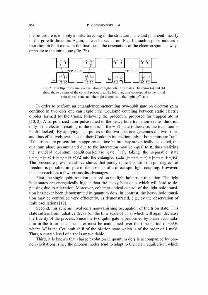
P. MACHNIKOWSKI et al. 854
the procedure is to apply a pulse traveling in the structure plane and polarized linearly in the growth direction. Again, as can be seen from Fig. 1d, such a pulse induces a transition in both cases. In the final state, the orientation of the electron spin is always opposite to the initial one (Fig. 2b).
Fig. 2. Spin flip procedure via excitation of light hole trion states. Diagrams (a) and (b) show the two steps of the control procedure. The left diagrams correspond to the initial
“spin down” state, and the right diagrams to the “spin up” state
In order to perform an entanglement-generating two-qubit gate on electron spins confined in two dots one can exploit the Coulomb coupling between static electric dipoles formed by the trions, following the procedure proposed for trapped atoms [10, 2]. A σ+ polarized laser pulse tuned to the heavy hole transition excites the trion only if the electron residing in the dot is in the +1/2 state (otherwise, the transition is Pauli-blocked). By applying such pulses to the two dots one generates the two trions and thus effectively switches on their Coulomb interaction only if both spins are “up”. If the trions are present for an appropriate time before they are optically deexcited, the quantum phase accumulated due to the interaction may be equal to π, thus realizing the standard quantum conditional-phase gate [11], taking the separable state (|− −⟩ + |− +⟩ + |+ −⟩ + |+ +⟩)/2 into the entangled state (|− −⟩ + |− +⟩ + |+ −⟩ − |+ +⟩)/2. The procedure presented above shows that purely optical control of spin degrees of freedom is possible, in spite of the absence of a direct spin-light coupling. However, this approach has a few serious disadvantages.
First, the single-qubit rotation is based on the light hole trion transition. The light hole states are energetically higher than the heavy hole ones which will lead to de-phasing due to relaxation. Moreover, coherent optical control of the light hole transi-tion has never been demonstrated in quantum dots. In contrast, the heavy hole transi-tion may be controlled very efficiently, as demonstrated, e.g., by the observation of Rabi oscillations [12].
Second, this scheme involves a non-vanishing occupation of the trion state. This state suffers from radiative decay (on the time scale of 1 ns) which will again decrease the fidelity of the process. Since the two-qubit gate is performed by phase accumula-tion in the trion state, the latter must be maintained over the time period of π/ΔE, where ΔE is the Coulomb shift of the bi-trion state which is of the order of 1 meV. Thus, a certain level of error is unavoidable.
Third, it is known that charge evolution in quantum dots is accompanied by pho-non excitations, since the phonon modes tend to adapt to their new equilibrium which
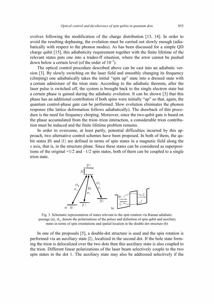
Optical control and decoherence of spin qubits in quantum dots 855
evolves following the modification of the charge distribution [13, 14]. In order to avoid the resulting dephasing, the evolution must be carried out slowly enough (adia-batically with respect to the phonon modes). As has been discussed for a simple QD charge qubit [15], this adiabaticity requirement together with the finite lifetime of the relevant states puts one into a tradeo-ff situation, where the error cannot be pushed down below a certain level (of the order of 10–3).
The optical control procedure described above can be cast into an adiabatic ver-sion [3]. By slowly switching on the laser field and smoothly changing its frequency (chirping) one adiabatically takes the initial “spin up” state into a dressed state with a certain admixture of the trion state. According to the adiabatic theorem, after the laser pulse is switched off, the system is brought back to the single electron state but a certain phase is gained during the adiabatic evolution. It can be shown [3] that this phase has an additional contribution if both spins were initially “up” so that, again, the quantum control-phase gate can be performed. Slow evolution eliminates the phonon response (the lattice deformation follows adiabatically). The drawback of this proce-dure is the need for frequency chirping. Moreover, since the two-qubit gate is based on the phase accumulated from the trion–trion interaction, a considerable trion contribu-tion must be induced and the finite lifetime problem remains.
In order to overcome, at least partly, potential difficulties incurred by this ap-proach, two alternative control schemes have been proposed. In both of them, the qu-bit states |0⟩ and |1⟩ are defined in terms of spin states in a magnetic field along the x axis, that is, in the structure plane. Since these states can be considered as superposi-tions of the original +1/2 and –1/2 spin states, both of them can be coupled to a single trion state.
Fig. 3. Schematic representation of states relevant to the spin rotation via Raman adiabatic passage (a), σx,y denote the polarizations of the pulses and definition of spin qubit and auxiliary
states in terms of spin orientations and spatial location in the double dot structure (b)
In one of the proposals [5], a double-dot structure is used and the spin rotation is performed via an auxiliary state |2⟩, localized in the second dot. If the hole state form-ing the trion is delocalized over the two dots then this auxiliary state is also coupled to the trion. Different linear polarizations of the laser beam selectively couple to the two spin states in the dot 1. The auxiliary state may also be addressed selectively if the
P. MACHNIKOWSKI et al. 856
transition energy in the second dot is different, which is easy to achieve. The diagram of energy levels and laser beams used in this scheme is shown in Fig. 3.
It has been shown within a general framework [16] that such a “three-leg” system allows one to couple nonresonantly (with a detuning Δ between the transition energy and the laser frequency) a selected (bright) superposition of the qubit states, |ψ⟩ = cosθ |0⟩ + e–iϕsinθ |1⟩, to the trion state, transfer it via adiabatic Raman passage to the auxiliary state and bring it back with a different phase of the laser pulse. As a result of such a procedure, this specific superposition gains a certain phase α with respect to the orthogonal (dark) one, |ψ⊥⟩ = sinθ |0⟩ − e–iϕcosθ |1⟩. It is straightforward to see that the unitary operator corresponding to the resulting transformation can be written as
|ψ⟩⟨ψ|eiα + |ψ⊥⟩⟨ψ⊥| = eiα/2 [cos(α/2)I − isin(α/2) nσ], where I is the unit operator, σ is the vector of Pauli matrices, and n = (sin2θcosϕ, sin2θsinϕ, cos2θ). Thus, the procedure results in a rotation of the spin by the angle α around the direction defined by the vector n. All the parameters of the rotation can be set by the appropriate choice of relative pulse amplitudes and phases, while the abso-lute amplitude 2 2 2 1/2
0 1 2 ( )Ω Ω Ω Ω= + + and the detuning Δ remain arbitrary. An essen-tial feature of this procedure is that for any parameters, the evolution starting in the subspace spanned by |0⟩ and |1⟩ remains in the subspace spanned by the single-electron states |0⟩, |1⟩ and |2⟩ (in a trapped state [17]). Thus, the trion state is never occupied, which eliminates the errors due to its finite lifetime. In Sec. 5, we will see that the procedure may be performed in such a way that phonon decoherence is sup-pressed to a large extent.
The other proposal [6] is based on the same idea of performing the spin rotation by changing the phase of a selected superposition of the spin state. Now, however, the auxiliary state is absent, which removes the requirement for a very special, delocalized hole state. An arbitrary spin rotation is achieved by an adiabatic evolution within the “lambda system” (so called because of the form of its graphical representation) formed by the two spin states and the trion state. The dynamics of the system may be unders-tood in terms of the AC Stark shift: Since the bright superposition state is coupled to the laser field, its energy is shifted. Hence, during the time when the laser pulse is present it accumulates an additional dynamical phase with respect to the dark state. The coupling is again nonresonant and the evolution is adiabatic. The accumulate phase, hence the angle of rotation of the spin, depends on the interplay of the detuning and the absolute pulse intensity, so that one of these parameters may be considered arbitrary and serve for optimization against dephasing.
In general, this approach assumes a nonvanishing occupation of the trion state dur-ing the procedure but for large enough detuning this admixture of the trion state is small. Still, the question arises to what extent this small trion admixture may destroy the quantum coherence due to its radiative decay. Moreover, as in all the other cases, the dephasing due to phonon response to the charge evolution is an issue. This will be discussed in Sec. 5.
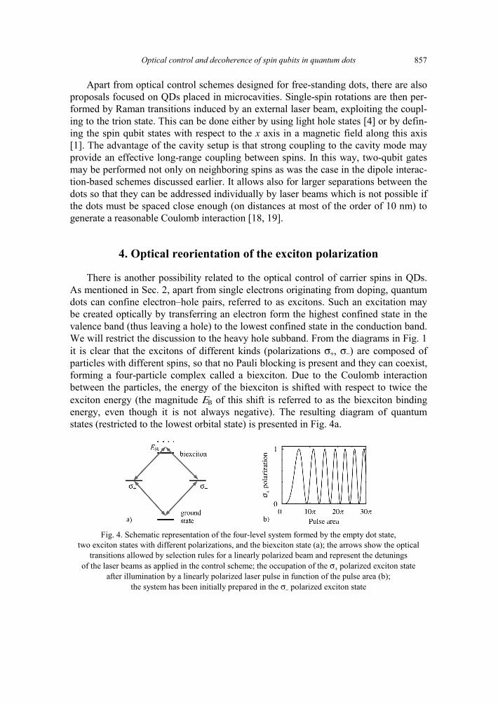
Optical control and decoherence of spin qubits in quantum dots 857
Apart from optical control schemes designed for free-standing dots, there are also proposals focused on QDs placed in microcavities. Single-spin rotations are then per-formed by Raman transitions induced by an external laser beam, exploiting the coupl-ing to the trion state. This can be done either by using light hole states [4] or by defin-ing the spin qubit states with respect to the x axis in a magnetic field along this axis [1]. The advantage of the cavity setup is that strong coupling to the cavity mode may provide an effective long-range coupling between spins. In this way, two-qubit gates may be performed not only on neighboring spins as was the case in the dipole interac-tion-based schemes discussed earlier. It allows also for larger separations between the dots so that they can be addressed individually by laser beams which is not possible if the dots must be spaced close enough (on distances at most of the order of 10 nm) to generate a reasonable Coulomb interaction [18, 19].
4. Optical reorientation of the exciton polarization
There is another possibility related to the optical control of carrier spins in QDs. As mentioned in Sec. 2, apart from single electrons originating from doping, quantum dots can confine electron–hole pairs, referred to as excitons. Such an excitation may be created optically by transferring an electron form the highest confined state in the valence band (thus leaving a hole) to the lowest confined state in the conduction band. We will restrict the discussion to the heavy hole subband. From the diagrams in Fig. 1 it is clear that the excitons of different kinds (polarizations σ+, σ−) are composed of particles with different spins, so that no Pauli blocking is present and they can coexist, forming a four-particle complex called a biexciton. Due to the Coulomb interaction between the particles, the energy of the biexciton is shifted with respect to twice the exciton energy (the magnitude ΕΒ of this shift is referred to as the biexciton binding energy, even though it is not always negative). The resulting diagram of quantum states (restricted to the lowest orbital state) is presented in Fig. 4a.
Fig. 4. Schematic representation of the four-level system formed by the empty dot state,
two exciton states with different polarizations, and the biexciton state (a); the arrows show the optical transitions allowed by selection rules for a linearly polarized beam and represent the detunings
of the laser beams as applied in the control scheme; the occupation of the σ+ polarized exciton state after illumination by a linearly polarized laser pulse in function of the pulse area (b);
the system has been initially prepared in the σ− polarized exciton state
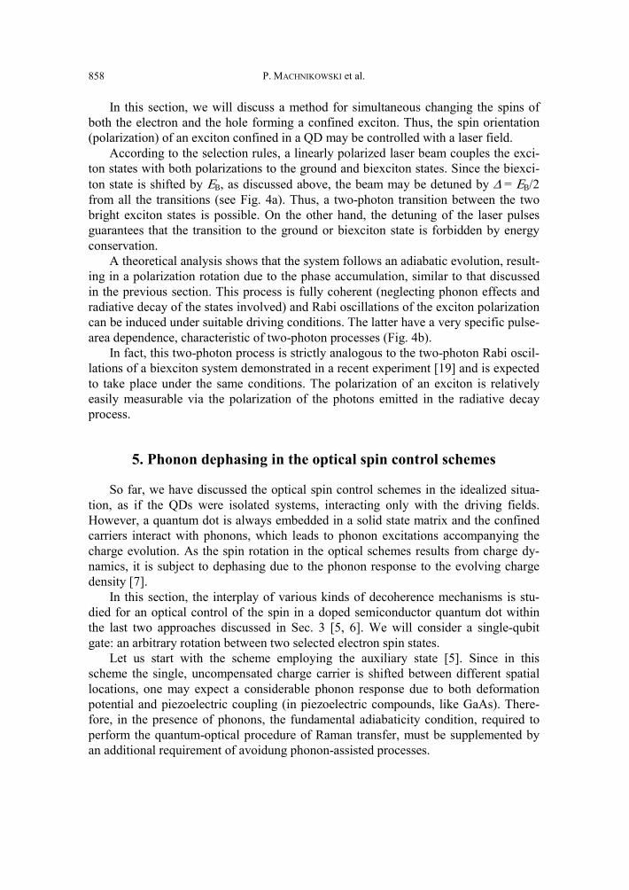
P. MACHNIKOWSKI et al. 858
In this section, we will discuss a method for simultaneous changing the spins of both the electron and the hole forming a confined exciton. Thus, the spin orientation (polarization) of an exciton confined in a QD may be controlled with a laser field.
According to the selection rules, a linearly polarized laser beam couples the exci-ton states with both polarizations to the ground and biexciton states. Since the biexci-ton state is shifted by ΕΒ, as discussed above, the beam may be detuned by Δ = ΕΒ/2 from all the transitions (see Fig. 4a). Thus, a two-photon transition between the two bright exciton states is possible. On the other hand, the detuning of the laser pulses guarantees that the transition to the ground or biexciton state is forbidden by energy conservation.
A theoretical analysis shows that the system follows an adiabatic evolution, result-ing in a polarization rotation due to the phase accumulation, similar to that discussed in the previous section. This process is fully coherent (neglecting phonon effects and radiative decay of the states involved) and Rabi oscillations of the exciton polarization can be induced under suitable driving conditions. The latter have a very specific pulse-area dependence, characteristic of two-photon processes (Fig. 4b).
In fact, this two-photon process is strictly analogous to the two-photon Rabi oscil-lations of a biexciton system demonstrated in a recent experiment [19] and is expected to take place under the same conditions. The polarization of an exciton is relatively easily measurable via the polarization of the photons emitted in the radiative decay process.
5. Phonon dephasing in the optical spin control schemes
So far, we have discussed the optical spin control schemes in the idealized situa-tion, as if the QDs were isolated systems, interacting only with the driving fields. However, a quantum dot is always embedded in a solid state matrix and the confined carriers interact with phonons, which leads to phonon excitations accompanying the charge evolution. As the spin rotation in the optical schemes results from charge dy-namics, it is subject to dephasing due to the phonon response to the evolving charge density [7].
In this section, the interplay of various kinds of decoherence mechanisms is stu-died for an optical control of the spin in a doped semiconductor quantum dot within the last two approaches discussed in Sec. 3 [5, 6]. We will consider a single-qubit gate: an arbitrary rotation between two selected electron spin states.
Let us start with the scheme employing the auxiliary state [5]. Since in this scheme the single, uncompensated charge carrier is shifted between different spatial locations, one may expect a considerable phonon response due to both deformation potential and piezoelectric coupling (in piezoelectric compounds, like GaAs). There-fore, in the presence of phonons, the fundamental adiabaticity condition, required to perform the quantum-optical procedure of Raman transfer, must be supplemented by an additional requirement of avoidung phonon-assisted processes.
Optical control and decoherence of spin qubits in quantum dots 859
A formal analysis [20] has shown that the carrier–phonon coupling indeed gives rise to pure dephasing as well as to transitions between the trapped carrier-field states. The former decreases for slower driving [15], while the contribution from the latter is approximately proportional to the process duration. The probability of phonon-induced transitions becomes very high if the spacing between the trapped energy le-vels falls into the area of high phonon spectral density. For a double-dot structure, the latter has a complicated, oscillatory form. Moreover, in an attempt to optimize the control parameters one encounters a trade-off situation, due to the opposite require-ments for phonon-induced jumps (short duration) and for the fundamental adiabaticity condition and pure dephasing (slow operation). Therefore, in order to estimate the fidelity of the spin rotation and to find optimal parameters for the control procedure one has to perform detailed quantitative calculations taking into account the details of the system structure.
Fig. 5. The error for the spin rotation performed using the Raman adiabatic passage scheme
in function of the laser pulse parameters (a) for the pulse durations of 50 ps at 1 K and the error for a π/2 spin rotation without the auxiliary state (b) in function of the detuning for
a few pulse durations. Both results correspond to a self-assembled InAs/GaAs structure
As was mentioned in Sec. 3, this control procedure allows a free choice of the ab-solute beam intensity Ω and of the detuning Δ. Together with the arbitrary duration of the control pulses, this yields three free parameters. The phonon-induced decoherence effects may be determined using the general perturbative approach that allows one to calculate the phonon perturbation for an arbitrary driven evolution of the system [7]. In Fig. 5a we plot the error δ = 1−F2, where F is the fidelity of the operation (a stan-dard measure of the overlap between the desired final state and the actual one [11]), minimized over the pulse durations, as a function of the other two parameters. It is clear that this procedure may be performed with errors very low compared to the thre-shold value of 10–4 or 10–3 [21] required for the implementation of quantum error-correction schemes and thus for a scalable implementation of quantum computing. However, such a high fidelity is achievable only in very narrow ranges of parameter values.
In the control scheme without the auxiliary state [6], there are again contributions to the error from the dynamical phonon response (pure dephasing), from jumps be-
P. MACHNIKOWSKI et al. 860
tween the adiabatic states, and from the imperfect adiabaticity of the evolution. The jumps may now be interpreted as phonon-assisted trion generation and their impact is particularly large for positive detuning, when a transition to the trion state may take place upon absorption of a photon and emission of a phonon, which is possible even at zero temperature. Another contribution to decoherence now originates from the finite lifetime of the trion since, in contrast to the previous control scheme, a certain occupa-tion of the trion state appears during the evolution.
In order to assess the importance of all these contributions one has to perform detailed calculations, including the carrier-phonon couplings, radiative decay of the trion state and corrections from the nonadiabaticity of the evolution. Since the angle of rotation of the spin now depends on a combination of the absolute pulse intensity and detuning only one of these parameters may be considered free. Another free parameter is the pulse duration. In Figure 5b, we plot the error for a π/2 rotation, averaged over the initial state, as a func-tion of the detuning Δ (pulse amplitudes are then adjusted to achieve the π/2 rotation) for a few values of the pulse duration. A positive detuning means a red-shift of the laser fre-quencies with respect to the trion transition. As a result of the complicated interplay of the different contributions, the error now depends on the detuning in a quite irregular way. It turns out that the fidelity of the operation strongly depends on the pulse duration only for sub-meV detuning, where the error is relatively high. A very high fidelity may be achieved for a detuning of the order of 10 meV [23].
6. Conclusion
We have reviewed a few theoretical proposals showing that optical control of in-dividual spins and exciton polarizations in quantum dots is possible, at least in prin-ciple. We have shown that careful optimization of parameters may bring the errors of such optical spin rotations (including those related to carrier-phonon interactions) to very low levels. Some of these proposals are very demanding with respect to the sys-tem properties and, so far, none of them has been realized experimentally. However, the rapid progress of the engineering of QD structures and coherent optical control of quantum dots that can be observed in recent years will certainly make the implementa-tion of such control techniques feasible in the close future.
References
[1] IMAMOĞLU A., AWSCHALOM D.D., BURKARD G., DIVINCENZO D.P., LOSS D., SHERWIN M., SMALL A., Phys. Rev. Lett., 83 (1999), 4202.
[2] PAZY E., BIOLATTI E., CALARCO T., D'AMICO I., ZANARDI P., ROSSI F., ZOLLER P., Europhys. Lett., 62 (2003), 175.
[3] CALARCO T., DATTA A., FEDICHEV P., PAZY E., ZOLLER P., Phys. Rev. A, 68 (2003), 012310. [4] FENG M., D’AMICO I., ZANARDI P., ROSSI F., Phys. Rev. A, 67 (2003), 014306. [5] TROIANI F., MOLINARI E., HOHENESTER U., Phys. Rev. Lett., 90 (2003), 206802.
Optical control and decoherence of spin qubits in quantum dots 861
[6] CHEN P., PIERMAROCCHI C., SHAM L.J., GAMMON D., STEEL D.G., Phys. Rev. B, 69 (2004) 075320. [7] GRODECKA A., JACAK L., MACHNIKOWSKI P., ROSZAK K., [in:] Quantum Dots: Research Develop-
ments, P. A. Ling (Ed.), Nova Science, New York, 2005, p. 47; cond-mat/0404364. [8] JACAK L., HAWRYLAK P., WÓJS A., Quantum Dots, Springer, Berlin, 1998. [9] CHEN G., BONADEO N.H., STEEL D.G., GAMMON D., KATZER D.S., PARK D., SHAM L.J., Science,
289 (2000), 1906. [10] JAKSCH D., CIRAC J.I., ZOLLER, P., ROLSTON S.L., CÔTÉ R., LUKIN M.D., Phys. Rev. Lett., 85 (2000), 2208. [11] NIELSEN M.A., CHUANG I.L., Quantum Computation and Quantum Information, Cambridge Univer-
sity Press, Cambridge, 2000. [12] ZRENNER A., BEHAM E., STUFFLER S., FINDEIS F., BICHLER M., ABSTREITER G., Nature, 418 (2002), 612. [13] JACAK L., MACHNIKOWSKI P., KRASNYJ J., ZOLLER P., Eur. Phys. J. D, 22 (2003), 319. [14] VAGOV A., AXT V.M., KUHN T., Phys. Rev. B, 66 (2002), 165312. [15] ALICKI R., HORODECKI M., HORODECKI P., HORODECKI R., JACAK L., MACHNIKOWSKI P., Phys. Rev.
A, 70 (2004), 010501(R). [16] KIS Z., RENZONI F., Phys. Rev. A, 65 (2002), 032318. [17] SCULLY M.O.AND ZUBAIRY M.S., Quantum Optics, Cambridge University Press, Cambridge, 1997. [18] DANCKWERTS J., AHN K.J., FÖRSTNER J., KNORR A., Phys. Rev. B 73 (2006), 165318. [19] RICHTER M., AHN K.J., KNORR A., SCHLIWA A., BIMBERG D., MADJET M.E., RENGER T., Phys. Stat.
Sol. (b) 243 (2006), 2302. [20] STUFLER S., MACHNIKOWSKI P., ESTER P., BICHLER M., AXT V.M., KUHN T., ZRENNER A., Phys.
Rev. B, 73 (2006), 125304. [21] ROSZAK K., GRODECKA A., MACHNIKOWSKI P., KUHN T., Phys. Rev. B, 71 (2005), 195333. [22] KNILL E., Nature, 434 (2005), 39.
Received 10 May 2007 Revised 17 October 2007
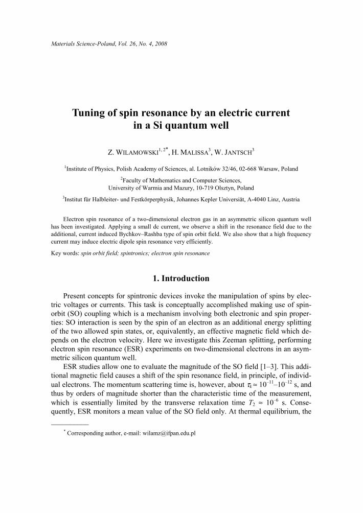
Materials Science-Poland, Vol. 26, No. 4, 2008
Tuning of spin resonance by an electric current in a Si quantum well
Z. WILAMOWSKI1, 2*, H. MALISSA3, W. JANTSCH3
1Institute of Physics, Polish Academy of Sciences, al. Lotników 32/46, 02-668 Warsaw, Poland 2Faculty of Mathematics and Computer Sciences,
University of Warmia and Mazury, 10-719 Olsztyn, Poland
3Institut für Halbleiter- und Festkörperphysik, Johannes Kepler Universiät, A-4040 Linz, Austria
Electron spin resonance of a two-dimensional electron gas in an asymmetric silicon quantum well has been investigated. Applying a small dc current, we observe a shift in the resonance field due to the additional, current induced Bychkov–Rashba type of spin orbit field. We also show that a high frequency current may induce electric dipole spin resonance very efficiently.
Key words: spin orbit field; spintronics; electron spin resonance
1. Introduction
Present concepts for spintronic devices invoke the manipulation of spins by elec-tric voltages or currents. This task is conceptually accomplished making use of spin-orbit (SO) coupling which is a mechanism involving both electronic and spin proper-ties: SO interaction is seen by the spin of an electron as an additional energy splitting of the two allowed spin states, or, equivalently, an effective magnetic field which de-pends on the electron velocity. Here we investigate this Zeeman splitting, performing electron spin resonance (ESR) experiments on two-dimensional electrons in an asym-metric silicon quantum well.
ESR studies allow one to evaluate the magnitude of the SO field [1–3]. This addi-tional magnetic field causes a shift of the spin resonance field, in principle, of individ-ual electrons. The momentum scattering time is, however, about τk ≈ 10–11–10–12 s, and thus by orders of magnitude shorter than the characteristic time of the measurement, which is essentially limited by the transverse relaxation time T2 ≈ 10–6 s. Conse-quently, ESR monitors a mean value of the SO field only. At thermal equilibrium, the __________
* Corresponding author, e-mail: [email protected]
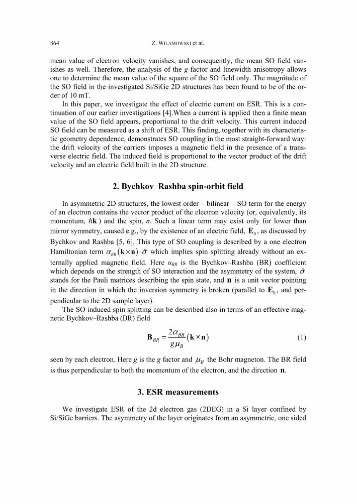
Z. WILAMOWSKI et al. 864
mean value of electron velocity vanishes, and consequently, the mean SO field van-ishes as well. Therefore, the analysis of the g-factor and linewidth anisotropy allows one to determine the mean value of the square of the SO field only. The magnitude of the SO field in the investigated Si/SiGe 2D structures has been found to be of the or-der of 10 mT.
In this paper, we investigate the effect of electric current on ESR. This is a con-tinuation of our earlier investigations [4].When a current is applied then a finite mean value of the SO field appears, proportional to the drift velocity. This current induced SO field can be measured as a shift of ESR. This finding, together with its characteris-tic geometry dependence, demonstrates SO coupling in the most straight-forward way: the drift velocity of the carriers imposes a magnetic field in the presence of a trans-verse electric field. The induced field is proportional to the vector product of the drift velocity and an electric field built in the 2D structure.
2. Bychkov–Rashba spin-orbit field
In asymmetric 2D structures, the lowest order – bilinear – SO term for the energy of an electron contains the vector product of the electron velocity (or, equivalently, its momentum, k ) and the spin, σ. Such a linear term may exist only for lower than mirror symmetry, caused e.g., by the existence of an electric field, 0E , as discussed by Bychkov and Rashba [5, 6]. This type of SO coupling is described by a one electron Hamiltonian term ( )BRα σ× ⋅k n which implies spin splitting already without an ex-ternally applied magnetic field. Here αBR is the Bychkov–Rashba (BR) coefficient which depends on the strength of SO interaction and the asymmetry of the system, σ stands for the Pauli matrices describing the spin state, and n is a unit vector pointing in the direction in which the inversion symmetry is broken (parallel to 0E , and per-pendicular to the 2D sample layer).
The SO induced spin splitting can be described also in terms of an effective mag-netic Bychkov–Rashba (BR) field
( )2 BRBR
Bgαμ
=B k ×n (1)
seen by each electron. Here g is the g factor and Bμ the Bohr magneton. The BR field is thus perpendicular to both the momentum of the electron, and the direction .n
3. ESR measurements
We investigate ESR of the 2d electron gas (2DEG) in a Si layer confined by Si/SiGe barriers. The asymmetry of the layer originates from an asymmetric, one sided
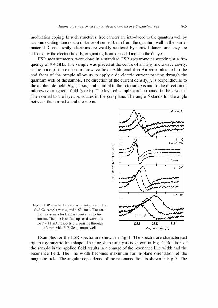
Tuning of spin resonance by an electric current in a Si quantum well 865
modulation doping. In such structures, free carriers are introduced to the quantum well by accommodating donors at a distance of some 10 nm from the quantum well in the barrier material. Consequently, electrons are weakly scattered by ionised donors and they are affected by the electric field E0 originating from ionised donors in the δ layer.
ESR measurements were done in a standard ESR spectrometer working at a fre-quency of 9.4 GHz. The sample was placed at the centre of a TE102 microwave cavity, at the node of the electric microwave field. Additional thin Au wires attached to the end faces of the sample allow us to apply a dc electric current passing through the quantum well of the sample. The direction of the current density, j, is perpendicular to the applied dc field, B0z, (z axis) and parallel to the rotation axis and to the direction of microwave magnetic field (y axis). The layered sample can be rotated in the cryostat. The normal to the layer, n, rotates in the (xz) plane. The angle θ stands for the angle between the normal n and the z axis.
Fig. 1. ESR spectra for various orientations of the Si/SiGe sample with nS = 5×1011 cm–2. The cen-
tral line stands for ESR without any electric current. The line is shifted up- or downwards for J = ±1 mA, respectively, passing through
a 3 mm wide Si/SiGe quantum well
Examples for the ESR spectra are shown in Fig. 1. The spectra are characterized by an asymmetric line shape. The line shape analysis is shown in Fig. 2. Rotation of the sample in the applied field results in a change of the resonance line width and the resonance field. The line width becomes maximum for in-plane orientation of the magnetic field. The angular dependence of the resonance field is shown in Fig. 3. The
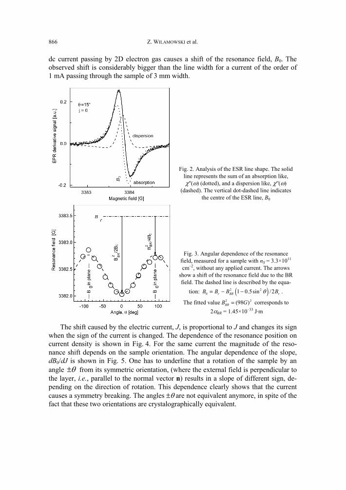
Z. WILAMOWSKI et al. 866
dc current passing by 2D electron gas causes a shift of the resonance field, B0. The observed shift is considerably bigger than the line width for a current of the order of 1 mA passing through the sample of 3 mm width.
Fig. 2. Analysis of the ESR line shape. The solid line represents the sum of an absorption like, χ′′(ω) (dotted), and a dispersion like, χ′′(ω)
(dashed). The vertical dot-dashed line indicates the centre of the ESR line, B0
Fig. 3. Angular dependence of the resonance field, measured for a sample with nS = 3.3×10¹¹
cm–2, without any applied current. The arrows show a shift of the resonance field due to the BR field. The dashed line is described by the equa-
tion: ( )2 20 1 0.5sin /2r BR rB B B Bθ= − − .
The fitted value 2 2(98 )BRB G= corresponds to 2αBR = 1.45×10⁻³³ J·m
The shift caused by the electric current, J, is proportional to J and changes its sign when the sign of the current is changed. The dependence of the resonance position on current density is shown in Fig. 4. For the same current the magnitude of the reso-nance shift depends on the sample orientation. The angular dependence of the slope, dB0/dJ is shown in Fig. 5. One has to underline that a rotation of the sample by an angle θ± from its symmetric orientation, (where the external field is perpendicular to the layer, i.e., parallel to the normal vector n) results in a slope of different sign, de-pending on the direction of rotation. This dependence clearly shows that the current causes a symmetry breaking. The angles ±θ are not equivalent anymore, in spite of the fact that these two orientations are crystalographically equivalent.
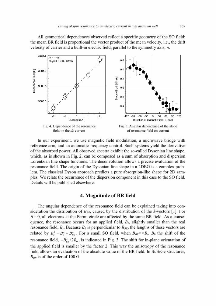
Tuning of spin resonance by an electric current in a Si quantum well 867
All geometrical dependences observed reflect a specific geometry of the SO field: the mean BR field is proportional the vector product of the mean velocity, i.e., the drift velocity of carrier and a built-in electric field, parallel to the symmetry axis, n.
Fig. 4. Dependence of the resonance
field on the dc current Fig. 5. Angular dependence of the slope
of resonance field on current
In our experiment, we use magnetic field modulation, a microwave bridge with reference arm, and an automatic frequency control. Such systems yield the derivative of the absorbed power. All observed spectra exhibit the so-called Dysonian line shape, which, as is shown in Fig. 2, can be composed as a sum of absorption and dispersion Lorentzian line shape functions. The deconvolution allows a precise evaluation of the resonance field. The origin of the Dysonian line shape in a 2DEG is a complex prob-lem. The classical Dyson approach predicts a pure absorption-like shape for 2D sam-ples. We relate the occurrence of the dispersion component in this case to the SO field. Details will be published elsewhere.
4. Magnitude of BR field
The angular dependence of the resonance field can be explained taking into con-sideration the distribution of BBR, caused by the distribution of the k-vectors [1]. For θ = 0, all electrons at the Fermi circle are affected by the same BR field. As a conse-quence, the resonance occurs for an applied field, B0, slightly smaller than the real resonance field, Br. Because B0 is perpendicular to BBR, the lengths of these vectors are related by 2 2 2
0r BRB B B= + . For a small SO field, when BBR<<Br, B0 the shift of the resonance field, 2
0/2BRB B− , is indicated in Fig. 3. The shift for in-plane orientation of the applied field is smaller by the factor 2. This way the anisotropy of the resonance field allows an evaluation of the absolute value of the BR field. In Si/SiGe structures, BBR is of the order of 100 G.
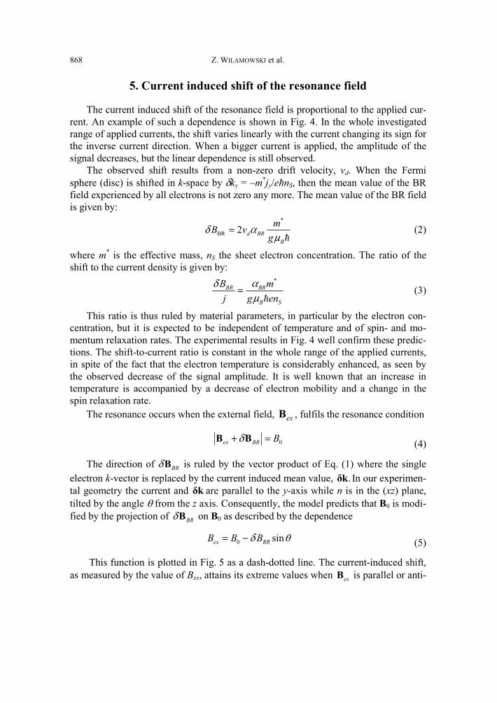
Z. WILAMOWSKI et al. 868
5. Current induced shift of the resonance field
The current induced shift of the resonance field is proportional to the applied cur-rent. An example of such a dependence is shown in Fig. 4. In the whole investigated range of applied currents, the shift varies linearly with the current changing its sign for the inverse current direction. When a bigger current is applied, the amplitude of the signal decreases, but the linear dependence is still observed.
The observed shift results from a non-zero drift velocity, vd. When the Fermi sphere (disc) is shifted in k-space by δky = –m*jy/eħnS, then the mean value of the BR field experienced by all electrons is not zero any more. The mean value of the BR field is given by:
*
BR 2 d BRB
mB vg
δ αμ
= (2)
where m* is the effective mass, nS the sheet electron concentration. The ratio of the shift to the current density is given by:
*
BR BR
B S
B mj g en
δ αμ
= (3)
This ratio is thus ruled by material parameters, in particular by the electron con-centration, but it is expected to be independent of temperature and of spin- and mo-mentum relaxation rates. The experimental results in Fig. 4 well confirm these predic-tions. The shift-to-current ratio is constant in the whole range of the applied currents, in spite of the fact that the electron temperature is considerably enhanced, as seen by the observed decrease of the signal amplitude. It is well known that an increase in temperature is accompanied by a decrease of electron mobility and a change in the spin relaxation rate.
The resonance occurs when the external field, exB , fulfils the resonance condition
0ex BR Bδ+ =B B (4)
The direction of BRδB is ruled by the vector product of Eq. (1) where the single electron k-vector is replaced by the current induced mean value, .δk In our experimen-tal geometry the current and δk are parallel to the y-axis while n is in the (xz) plane, tilted by the angle θ from the z axis. Consequently, the model predicts that B0 is modi-fied by the projection of BRδB on B0 as described by the dependence
0 sinex BRB B Bδ θ= − (5)
This function is plotted in Fig. 5 as a dash-dotted line. The current-induced shift, as measured by the value of Bex, attains its extreme values when exB is parallel or anti-
Tuning of spin resonance by an electric current in a Si quantum well 869
parallel to .BRB For θ = 0, the mean BR field, BRδB , is perpendicular to exB and, prac-tically, no shift is observed.
6. Conclusions
The occurrence of the current induced SO field has been theoretically predicted by Kalevich and Korenev [7]. They found also an influence of the electric current on the Hanle effect. Application of the concept of a current- (velocity-) induced field has been proposed in the Datta–Das transistor. Recently Kato et al. [8] found an effect of current on the precession of magnetization by ultra fast Faraday spectroscopy. Our results obtained by resonance measurements, however, are the most direct evaluation of the current induced SO field.
The fact that an electric current allows for tuning of the spin resonance has also practical aspects. First of all, controlling a current is technically much easier than ap-plying a magnetic field. Moreover, the current can be well applied to a local micro-element of a large electronic structure.
Finally, the fact that a dc current allows to generate a dc magnetic field allows one to predict that an ac current can lead to an ac SO field. The model estimations show that resonance excitation by an ac current can be by orders of magnitude more effec-tive for a high mobility electron gas than the classical resonance excitation by an ac magnetic field.
Acknowledgement
This work was supported by the Fonds zur Förderung der Wissenschaftlichen Forschung, and the ÖAD, both Vienna, Austria, and in Poland by MNiSW.
References
[1] WILAMOWSKI Z., JANTSCH W., MALISSA H., RÖSSLER U., Phys. Rev. B 66 (2002), 195315. [2] WILAMOWSKI Z., JANTSCH W., Phys. Rev. B 69, 035328 (2004) [3] SCHULTE M., LOK J.G.S., DENNINGER G., DIETSCHE W., Phys. Rev. Lett. 94 (2005), 137601. [4] WILAMOWSKI Z., MALISSA H., SCHÄFFLER F., JANTSCH W., Phys. Rev. Lett., 98 (2007), 187203. [5] BYCHKOV YU.L., RASHBA E.I., J. Phys. C17 (1984), 6039. [6] RASHBA E.I., SHEKA V.I., Electric-Dipole Spin Resonances, [in:] Landau Level Spectroscopy,
G. Landwehr, E.I. Rashba (Eds.), Elsevier, Amsterdam, 1991 and references therein. [7] KALEVICH V.K., KORENEV V.L., JETP Lett., 52 (1990), 230; Appl. Magn. Res. (Kazan Physical
-Technical Institute) 2 (1991), 397. [8] KATO Y., MYERS R.C., GOSSARD A.C., AWSCHALOM D.D., Nature, 427 (2004), 50.
Received 7 May 2007
Materials Science-Poland, Vol. 26, No. 4, 2008
Mesoscopic rings. Multi-states induced by quantum thermal fluctuations
J. DAJKA* , L. MACHURA, S. ROGOZIŃSKI, J. ŁUCZKA
Institute of Physics, University of Silesia, 40-007 Katowice, Poland
When temperature of a conducting mesoscopic ring is decreased, the magnetic flux states can change drastically, e.g. from bistable to multistable states. Possibility of the application of the multistability of the magnetic flux is emphasised in the information-theoretical context. A proposal of the quantum kinetics description is qualitatively discussed.
Key words: persistent current; quantum Smoluchowski limit; qutrit
Mesoscopic multiply connected samples such as conducting rings, cylinders or tori exhibit quantum size phenomena originating from the Aharonov–Bohm effects. One of the most spectacular phenomena is a persistent current [1] which is a direct manifestation of quantum phase coherence of the current carriers over a mesoscopic length scale. At a non-zero temperature, T > 0, the phase coherence of carriers is weakened and the samples exhibit the dissipative Ohmic contribution to the total cur-rent. There is a regime of temperatures in which both phase-coherent and dissipative Ohmic currents coexist. Such currents generate a magnetic flux. Its properties can be studied via modelling based on kinetic equations like Langevin equations [2]. The long-time, steady states of the magnetic flux are characterized by properties of the stationary probability density obtained from the corresponding Langevin equation. For instance, if the stationary probability density is bimodal, i.e., it has two maxima it reflects the possibility of occurrence of non-zero magnetic fluxes and in consequence the currents. One can notice an obvious analogy to the Josephson-based flux qubits [3]. There are serious advantages for using non-superconducting samples like rings as a building blocks for qubit storage because due to a small size they seem to be more stable with respect to decoherence and dephasing [4]. For higher temperatures, when __________
*Corresponding author, e-mail: [email protected]
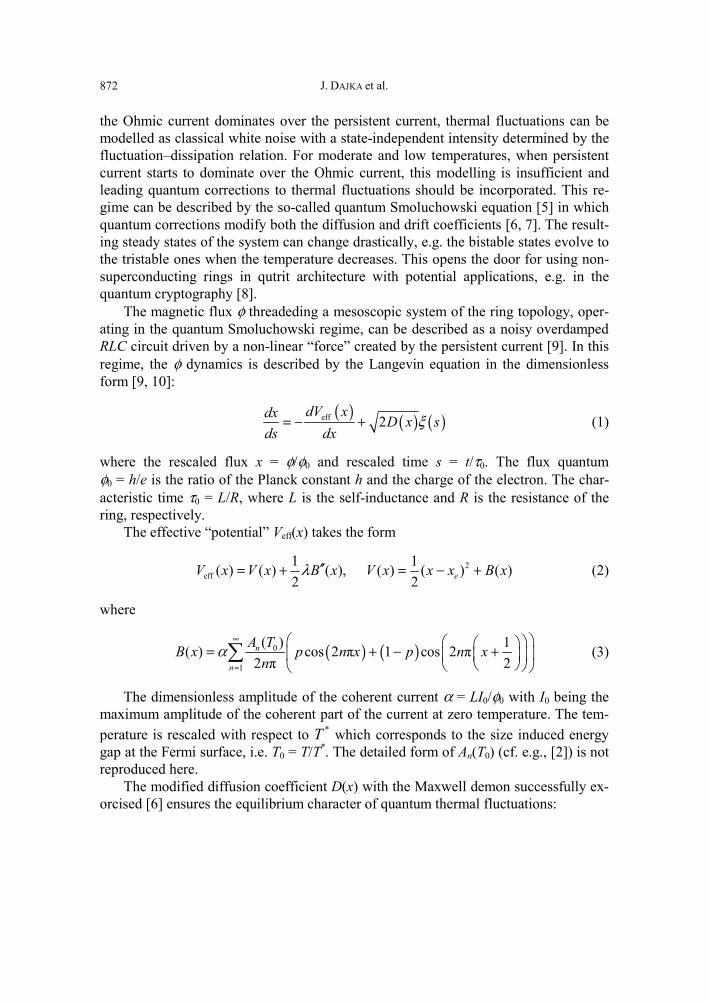
J. DAJKA et al. 872
the Ohmic current dominates over the persistent current, thermal fluctuations can be modelled as classical white noise with a state-independent intensity determined by the fluctuation–dissipation relation. For moderate and low temperatures, when persistent current starts to dominate over the Ohmic current, this modelling is insufficient and leading quantum corrections to thermal fluctuations should be incorporated. This re-gime can be described by the so-called quantum Smoluchowski equation [5] in which quantum corrections modify both the diffusion and drift coefficients [6, 7]. The result-ing steady states of the system can change drastically, e.g. the bistable states evolve to the tristable ones when the temperature decreases. This opens the door for using non-superconducting rings in qutrit architecture with potential applications, e.g. in the quantum cryptography [8].
The magnetic flux φ threadeding a mesoscopic system of the ring topology, oper-ating in the quantum Smoluchowski regime, can be described as a noisy overdamped RLC circuit driven by a non-linear “force” created by the persistent current [9]. In this regime, the φ dynamics is described by the Langevin equation in the dimensionless form [9, 10]:
( ) ( ) ( )eff 2dV xdx D x s
ds dxξ= − + (1)
where the rescaled flux x = φ/φ0 and rescaled time s = t/τ0. The flux quantum φ0 = h/e is the ratio of the Planck constant h and the charge of the electron. The char-acteristic time τ0 = L/R, where L is the self-inductance and R is the resistance of the ring, respectively.
The effective “potential” Veff(x) takes the form
2eff
1 1( ) ( ) ( ), ( ) ( ) ( )2 2 eV x V x B x V x x x B xλ ′′= + = − + (2)
where
( ) ( )0
1
( ) 1( ) cos 2 π 1 cos 2 π2 π 2n
n
A TB x p n x p n xn
α∞
=
⎛ ⎞⎛ ⎞⎛ ⎞= + − +⎜ ⎟⎜ ⎟⎜ ⎟⎝ ⎠⎝ ⎠⎝ ⎠
∑ (3)
The dimensionless amplitude of the coherent current α = LI0/φ0 with I0 being the maximum amplitude of the coherent part of the current at zero temperature. The tem-perature is rescaled with respect to *T which corresponds to the size induced energy gap at the Fermi surface, i.e. T0 = T/T*. The detailed form of An(T0) (cf. e.g., [2]) is not reproduced here.
The modified diffusion coefficient D(x) with the Maxwell demon successfully ex-orcised [6] ensures the equilibrium character of quantum thermal fluctuations:
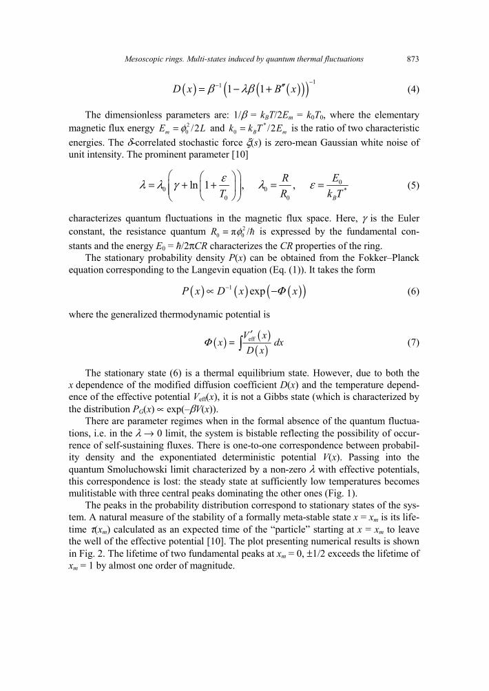
Mesoscopic rings. Multi-states induced by quantum thermal fluctuations 873
( ) ( )( )( ) 11 1 1D x B xβ λβ−− ′′= − + (4)
The dimensionless parameters are: 1/β = kBT/2Em = k0T0, where the elementary magnetic flux energy 2
0 /2mE Lφ= and *0 /2B mk k T E= is the ratio of two characteristic
energies. The δ-correlated stochastic force ξ(s) is zero-mean Gaussian white noise of unit intensity. The prominent parameter [10]
00 0 *
0 0
ln 1 , ,B
R ET R k Tελ λ γ λ ε
⎛ ⎞⎛ ⎞= + + = =⎜ ⎟⎜ ⎟⎜ ⎟⎝ ⎠⎝ ⎠
(5)
characterizes quantum fluctuations in the magnetic flux space. Here, γ is the Euler constant, the resistance quantum 2
0 0π /R φ= is expressed by the fundamental con-stants and the energy E0 = ħ/2πCR characterizes the CR properties of the ring.
The stationary probability density P(x) can be obtained from the Fokker–Planck equation corresponding to the Langevin equation (Eq. (1)). It takes the form
( ) ( ) ( )( )1 expP x D x xΦ−∝ − (6)
where the generalized thermodynamic potential is
( ) ( )( )
effV xx dx
D xΦ
′= ∫ (7)
The stationary state (6) is a thermal equilibrium state. However, due to both the x dependence of the modified diffusion coefficient D(x) and the temperature depend-ence of the effective potential Veff(x), it is not a Gibbs state (which is characterized by the distribution PG(x) ∝ exp(–βV(x)).
There are parameter regimes when in the formal absence of the quantum fluctua-tions, i.e. in the λ → 0 limit, the system is bistable reflecting the possibility of occur-rence of self-sustaining fluxes. There is one-to-one correspondence between probabil-ity density and the exponentiated deterministic potential V(x). Passing into the quantum Smoluchowski limit characterized by a non-zero λ with effective potentials, this correspondence is lost: the steady state at sufficiently low temperatures becomes mulitistable with three central peaks dominating the other ones (Fig. 1).
The peaks in the probability distribution correspond to stationary states of the sys-tem. A natural measure of the stability of a formally meta-stable state x = xm is its life-time τ(xm) calculated as an expected time of the “particle” starting at x = xm to leave the well of the effective potential [10]. The plot presenting numerical results is shown in Fig. 2. The lifetime of two fundamental peaks at xm = 0, ±1/2 exceeds the lifetime of xm = 1 by almost one order of magnitude.
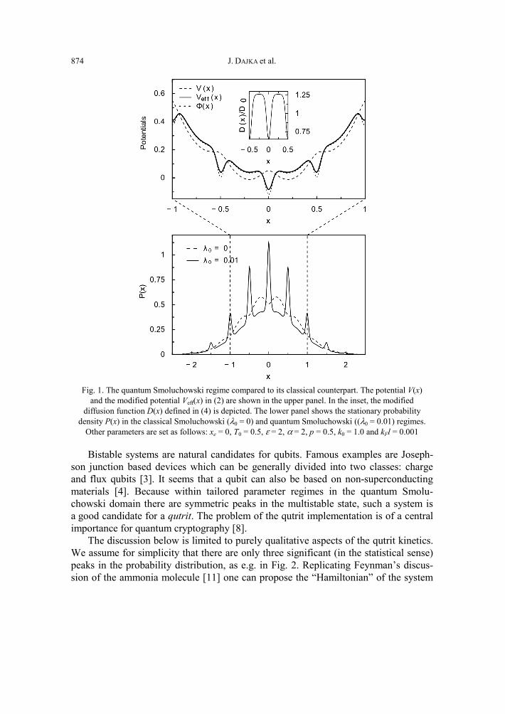
J. DAJKA et al. 874
Fig. 1. The quantum Smoluchowski regime compared to its classical counterpart. The potential V(x)
and the modified potential Veff(x) in (2) are shown in the upper panel. In the inset, the modified diffusion function D(x) defined in (4) is depicted. The lower panel shows the stationary probability
density P(x) in the classical Smoluchowski (λ0 = 0) and quantum Smoluchowski ((λ0 = 0.01) regimes. Other parameters are set as follows: xe = 0, T0 = 0.5, ε = 2, α = 2, p = 0.5, k0 = 1.0 and kFl = 0.001
Bistable systems are natural candidates for qubits. Famous examples are Joseph-son junction based devices which can be generally divided into two classes: charge and flux qubits [3]. It seems that a qubit can also be based on non-superconducting materials [4]. Because within tailored parameter regimes in the quantum Smolu-chowski domain there are symmetric peaks in the multistable state, such a system is a good candidate for a qutrit. The problem of the qutrit implementation is of a central importance for quantum cryptography [8].
The discussion below is limited to purely qualitative aspects of the qutrit kinetics. We assume for simplicity that there are only three significant (in the statistical sense) peaks in the probability distribution, as e.g. in Fig. 2. Replicating Feynman’s discus-sion of the ammonia molecule [11] one can propose the “Hamiltonian” of the system
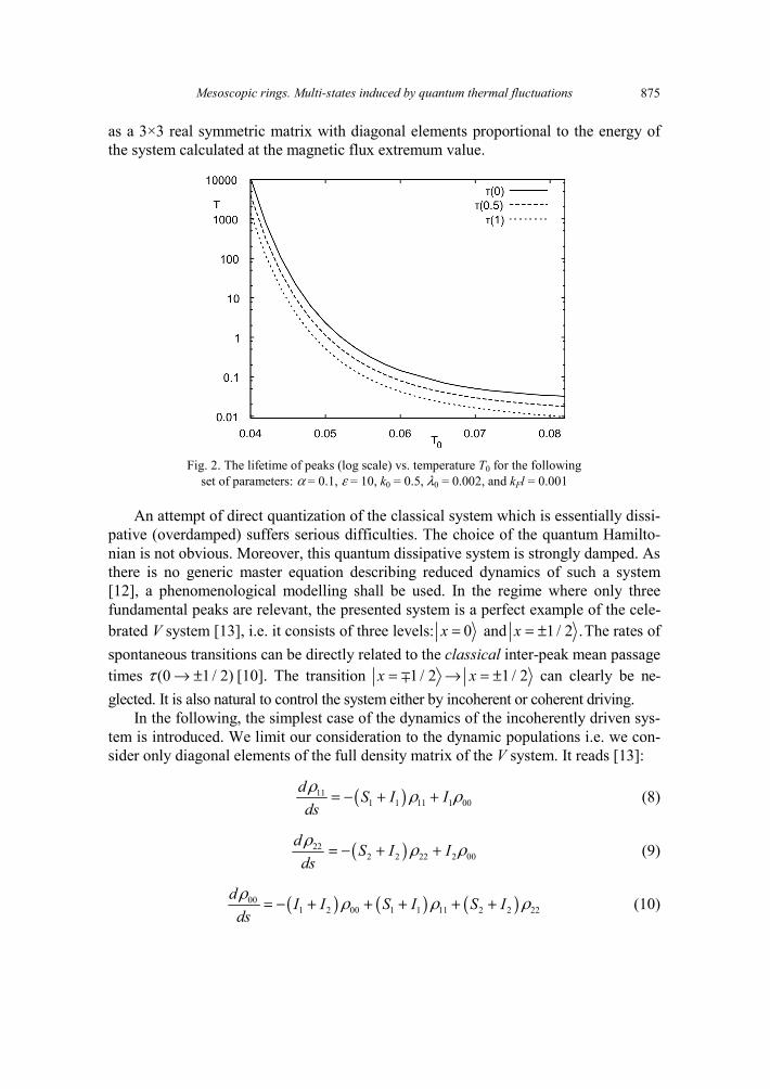
Mesoscopic rings. Multi-states induced by quantum thermal fluctuations 875
as a 3×3 real symmetric matrix with diagonal elements proportional to the energy of the system calculated at the magnetic flux extremum value.
Fig. 2. The lifetime of peaks (log scale) vs. temperature T0 for the following set of parameters: α = 0.1, ε = 10, k0 = 0.5, λ0 = 0.002, and kFl = 0.001
An attempt of direct quantization of the classical system which is essentially dissi-pative (overdamped) suffers serious difficulties. The choice of the quantum Hamilto-nian is not obvious. Moreover, this quantum dissipative system is strongly damped. As there is no generic master equation describing reduced dynamics of such a system [12], a phenomenological modelling shall be used. In the regime where only three fundamental peaks are relevant, the presented system is a perfect example of the cele-brated V system [13], i.e. it consists of three levels: 0x = and 1 / 2 .x = ± The rates of spontaneous transitions can be directly related to the classical inter-peak mean passage times (0 1 / 2)τ → ± [10]. The transition 1 / 2 1 / 2x x= → = ±∓ can clearly be ne-glected. It is also natural to control the system either by incoherent or coherent driving.
In the following, the simplest case of the dynamics of the incoherently driven sys-tem is introduced. We limit our consideration to the dynamic populations i.e. we con-sider only diagonal elements of the full density matrix of the V system. It reads [13]:
( )111 1 11 1 00
d S I Idsρ ρ ρ= − + + (8)
( )222 2 22 2 00
d S I Idsρ ρ ρ= − + + (9)
( ) ( ) ( )001 2 00 1 1 11 2 2 22
d I I S I S Idsρ ρ ρ ρ= − + + + + + (10)
J. DAJKA et al. 876
with the normalization condition 1.iii
ρ =∑ The parameters Ii and Si are the rates of
induced and spontaneous transitions, respectively. The stationary state [13]:
( ) ( )( ) ( )
1 2 211
1 2 2 2 2 22 2 3I S I
sS S I I S I
ρ+
→ ∞ =+ + +
(11)
( ) ( )( ) ( )
2 1 122
1 2 2 2 2 22 2 3I S I
sS S I I S I
ρ+
→ ∞ =+ + +
(12)
( ) ( )001
1 iii
s sρ ρ≥
→ ∞ = − → ∞∑ (13)
Despite its simplicity, the classical treatment described above allows an effective control of populations via a suitable external driving, e.g., finding “equidistribution” conditions 1/ 3iiρ = , satisfied e.g. for Ii >> Si. The potential application for quantum computing requires also an effective way of controlling coherences. It can be done either phenomenologically via suitable driving inducing inter-peak transitions or by consistent calculations beyond the quantum Smoluchowski expansion resulting in the master equation with non-diagonal elements included. Since the system is mesoscopic we expect the driving to operate at microwave [14] rather than optical frequencies.
The approach including kinetics of coherences can be formulated in terms of the phenomenological quantum jump formalism [13]. This problem is postponed to fur-ther studies.
Acknowledgement
The work supported by the MNiSzW under the grant No. 202 131 32/3786.
References
[1] HUND F., Ann. Phys. (Leipzig), 32 (1938), 102; KULIK I.O., JETP Lett., 11 (1970), 275; BÜTTIKER M., IMRY Y., LANDAUER R., Phys. Lett., A 96 (1993), 365.
[2] DAJKA J., ŁUCZKA J., SZOPA M., ZIPPER E., Phys. Rev B, 67 (2003), 073305; DAJKA J., KOSTUR M., ŁUCZKA J., SZOPA M., ZIPPER E., Acta Phys. Polon. B, 34 (2003), 3793.
[3] MAKHLIN Y., SCHÖN G., SCHNIRMAN A., Rev. Mod. Phys., 73 (2001), 357. [4] ZIPPER E., KURPAS M., SZELĄG M., DAJKA J., SZOPA M., Phys. Rev B, 74 (2006), 125462. [5] ANKERHOLD J., PECHUKAS P., GRABERT H., Phys. Rev. Lett., 87 (2001), 086801. [6] MACHURA Ł., KOSTUR M., HÄNGGI P., TALKNER P., ŁUCZKA J., Phys. Rev. E, 70 (2004), 031107;
ŁUCZKA J., RUDNICKI R., HÄNGGI P., Physica A, 351 (2005), 60. [7] ANKERHOLD J., Europhys. Lett. 67 (2004), 280; ANKERHOLD J., PECHUKAS P., GRABERT H., Chaos,
15 (2005), 026106. [8] MOLINA-TERRIZA G., VAZIRI A., URSIN R., ZEILINGER A., Phys. Rev. Lett., 94 (2005), 040501. [9] DAJKA J., ROGOZIŃSKI S., MACHURA Ł., ŁUCZKA J., Acta Phys. Polon. B, 38 (2007), 1737.
[10] DAJKA J., MACHURA Ł., ROGOZIŃSKI S., ŁUCZKA J., Phys. Rev. B, 76 (2007), 045337.

Mesoscopic rings. Multi-states induced by quantum thermal fluctuations 877
[11] FEYNMAN R.P., Lectures on Physics, Vol. 3, Addison-Wesley, Reading, 1964. [12] WEISS U., Quantum Dissipative Systems, 2nd Ed., World Scientific, Singapore, 1999. [13] PLENIO M.B., KNIGHT P.L., Rev. Mod. Phys., 70 (1998), 101. [14] DAJKA J., SZOPA M., VOURDAS A., ZIPPER E., Phys. Rev. B, 69 (2005), 045305; DAJKA J., ZIPPER E.,
Mater. Sci.-Poland, 24 (2006), 769.
Received 7 May 2007 Revised 19 September 2007
Materials Science-Poland, Vol. 26, No. 4, 2008
Phonon-assisted tunnelling through a quantum dot coupled to magnetic leads
W. RUDZIŃSKI*
Department of Physics, Adam Mickiewicz University, ul. Umułtowska 85, 61-614 Poznań, Poland
Spin-polarized transport has been theoretically studied in double barrier tunnelling junctions based on a single level quantum dot interacting with a local phonon mode. It was shown that the electron –phonon interaction gives rise to oscillations of the tunnel magnetoresistance (TMR). In asymmetrical junctions, the polaronic transport through the junction may lead to a significant suppression of the diode-like behaviour. The case of negative effective charging energy has also been analyzed numerically. It was shown in particular that for a mesoscopic diode an interplay between the single-electron cotunnelling and the pair tunnelling processes leads to inversion of TMR.
Key words: quantum dot; spin-polarized tunnelling; phonons
1. Introduction
Electronic transport through discrete levels of single molecules, carbon nanotubes or quantum dots (QDs) coupled to vibrational degrees of freedom has been investi-gated recently in a number of experimental as well as theoretical works (see, e.g., [1–3]). The present paper extends studies on phonon-assisted electronic transport in mesoscopic systems to the case of tunnelling through a single-level quantum dot cou-pled to ferromagnetic electrodes. One of the most widely studied spin-dependent ef-fects in such magnetic tunnel junctions is the tunnel magnetoresistance (TMR) [4]. Here, TMR is analyzed numerically in the context of polaronic transport through an interacting quantum dot and the both induced by the polaron shift cases of positive and negative effective charging energy are taken into account.
2. Model and method
Consider a single-level QD coupled to two ferromagnetic leads by tunnelling bar-riers, with the magnetic moments of the leads assumed to be aligned parallel (P) or __________
*E-mail: [email protected]
W. RUDZIŃSKI 880
antiparallel (AP). The whole system can be described by the model Hamiltonian of the form:
d ph el ph tH H H H H Hν −= + + + + (1)
The term Hν describes the left (ν = l) and right (ν = r) electrodes taken in the non-interacting quasiparticle limit
k k kk
H a aν σ ν σ ν σ νσ ν
ε +=∑ (2)
where εσkν is the single electron energy in the ν-th electrode for the wave vector k and spin σ (σ = ↑ , ↓ ). The term corresponding to the dot, Hd
d dH c c Uc c c cσ σσε + + +
↑ ↑ ↓ ↓= +∑ (3)
includes the spin-dependent single particle energy level εd, and Coulomb correlations described by the Hubbard parameter U. In order to include the effect of a phonon field, the model has been extended by
0phH b bω += (4)
where ω0 is a vibrational frequency of the phonon mode, whereas b+ and b are the corresponding phonon creation and anihilation operators. Moreover, the electron-phonon interaction part of the Hamiltonian (1) reads
( )el phH b b c cσ σλ + +− = + (5)
with the parameter λ denoting the strength of the electron-phonon coupling. Finally, the tunnelling part Ht includes spin-dependent tunnelling processes
h.c.t k kk
H T a cνσ σ ν σ
σ ν
+= +∑ (6)
Spin asymmetry of the tunnelling rates, 2
~ kΓ Tν νσ σ , is described by the parameters
pl and pr
( )0( ) 1llΓ Γ p↑ ↓ = ± (7)
( )0( ) 1rrΓ Γ pα↑ ↓ = ± (8)
where α denotes the ratio of tunnelling matrix elements through the right and left bar-riers, and where Г0 is a parameter.
To calculate the density matrix for the system we used non-equilibrium Green function technique based on the equation of motion in the Hartree–Fock approxima-tion. The assumption of strong electron-phonon interactions on the dot allowed us to
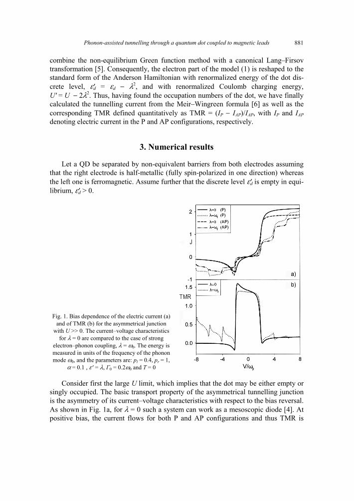
Phonon-assisted tunnelling through a quantum dot coupled to magnetic leads 881
combine the non-equilibrium Green function method with a canonical Lang–Firsov transformation [5]. Consequently, the electron part of the model (1) is reshaped to the standard form of the Anderson Hamiltonian with renormalized energy of the dot dis-crete level, ε′d = εd − λ2, and with renormalized Coulomb charging energy, U′ = U − 2λ2. Thus, having found the occupation numbers of the dot, we have finally calculated the tunnelling current from the Meir–Wingreen formula [6] as well as the corresponding TMR defined quantitatively as TMR = (IP − IAP)/IAP, with IP and IAP denoting electric current in the P and AP configurations, respectively.
3. Numerical results
Let a QD be separated by non-equivalent barriers from both electrodes assuming that the right electrode is half-metallic (fully spin-polarized in one direction) whereas the left one is ferromagnetic. Assume further that the discrete level ε′d is empty in equi-librium, ε′d > 0.
Fig. 1. Bias dependence of the electric current (a) and of TMR (b) for the asymmetrical junction
with U >> 0. The current–voltage characteristics for λ = 0 are compared to the case of strong
electron–phonon coupling, λ = ω0. The energy is measured in units of the frequency of the phonon mode ω0, and the parameters are: pl = 0.4, pr = 1,
α = 0.1 , ε ′ = λ, Γ0 = 0.2ω0 and T = 0
Consider first the large U limit, which implies that the dot may be either empty or singly occupied. The basic transport property of the asymmetrical tunnelling junction is the asymmetry of its current–voltage characteristics with respect to the bias reversal. As shown in Fig. 1a, for λ = 0 such a system can work as a mesoscopic diode [4]. At positive bias, the current flows for both P and AP configurations and thus TMR is
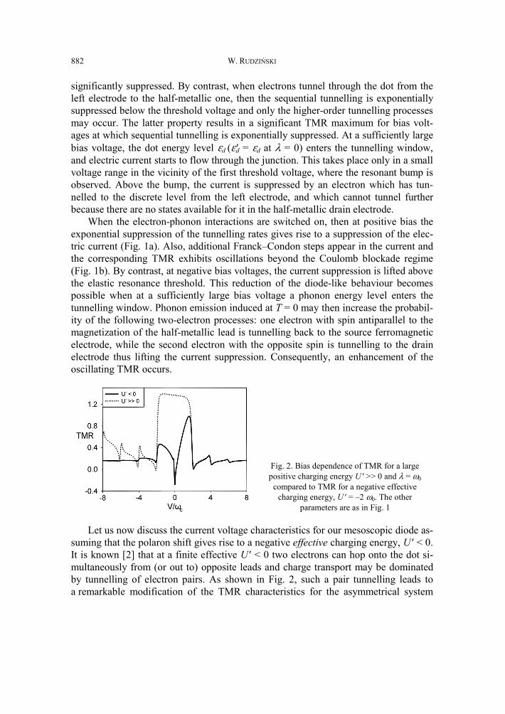
W. RUDZIŃSKI 882
significantly suppressed. By contrast, when electrons tunnel through the dot from the left electrode to the half-metallic one, then the sequential tunnelling is exponentially suppressed below the threshold voltage and only the higher-order tunnelling processes may occur. The latter property results in a significant TMR maximum for bias volt-ages at which sequential tunnelling is exponentially suppressed. At a sufficiently large bias voltage, the dot energy level εd (ε′d = εd at λ = 0) enters the tunnelling window, and electric current starts to flow through the junction. This takes place only in a small voltage range in the vicinity of the first threshold voltage, where the resonant bump is observed. Above the bump, the current is suppressed by an electron which has tun-nelled to the discrete level from the left electrode, and which cannot tunnel further because there are no states available for it in the half-metallic drain electrode.
When the electron-phonon interactions are switched on, then at positive bias the exponential suppression of the tunnelling rates gives rise to a suppression of the elec-tric current (Fig. 1a). Also, additional Franck–Condon steps appear in the current and the corresponding TMR exhibits oscillations beyond the Coulomb blockade regime (Fig. 1b). By contrast, at negative bias voltages, the current suppression is lifted above the elastic resonance threshold. This reduction of the diode-like behaviour becomes possible when at a sufficiently large bias voltage a phonon energy level enters the tunnelling window. Phonon emission induced at T = 0 may then increase the probabil-ity of the following two-electron processes: one electron with spin antiparallel to the magnetization of the half-metallic lead is tunnelling back to the source ferromagnetic electrode, while the second electron with the opposite spin is tunnelling to the drain electrode thus lifting the current suppression. Consequently, an enhancement of the oscillating TMR occurs.
Fig. 2. Bias dependence of TMR for a large positive charging energy U ′ >> 0 and λ = ω0
compared to TMR for a negative effective charging energy, U ′ = –2 ω0. The other
parameters are as in Fig. 1
Let us now discuss the current voltage characteristics for our mesoscopic diode as-suming that the polaron shift gives rise to a negative effective charging energy, U ′ < 0. It is known [2] that at a finite effective U ′ < 0 two electrons can hop onto the dot si-multaneously from (or out to) opposite leads and charge transport may be dominated by tunnelling of electron pairs. As shown in Fig. 2, such a pair tunnelling leads to a remarkable modification of the TMR characteristics for the asymmetrical system
Phonon-assisted tunnelling through a quantum dot coupled to magnetic leads 883
considered here. The central maximum of TMR (dotted curve in Fig. 2) originating from the single-electron higher-order tunnelling processes is now split due to pair-tunnelling into the two TMR maxima (solid curve in Fig. 2). In case of the asymmetrical magnetic junctions discussed here, pair-tunnelling processes are blocked at negative bias voltages since there are no states available for electrons with spins opposite to the mag-netization of the half-metallic drain lead. Then, only single-electron cotunnelling is possi-ble around V = 0. On the other hand, at small positive bias voltages, besides single-electron cotunnelling also pair-tunnelling is allowed contributing to a larger TMR ratio. Thus, an interplay between the single-electron cotunnelling and pair-tunnelling processes leads to inversion and asymmetry of TMR in the vicinity of V = 0, the visible in Fig. 2.
4. Conclusions
The polaronic transport through a tunnelling device based on an interacting single-level QD coupled to ferromagnetic electrodes results in a typical step-like electric current behaviour with additional Franck–Condon steps appearing at threshold bias voltages at which phonon-assisted electron transmission takes place. Consequently, oscillations of the corresponding tunnel magnetoresistance have been observed. It has also been found that the electron–phonon interactions in asymmetrical junctions may lift the current suppression above the threshold voltages at which the elastic resonance occurs, thus giving rise to a reduction of the diode-like behaviour.
When the polaron shift induces a negative effective charging energy, then a com-petition between the single-electron cotunnelling and pair-tunnelling processes leads to a splitting of the TMR maximum in the Coulomb blockade regime. The latter fea-ture may be accompanied by an inversion of the TMR ratio in the vicinity of zero bias voltage.
Acknowledgement
This work was supported by funds of the Polish Ministry of Science and Higher Education as a re-search project for years 2006–2009.
References
[1] FUJISAWA T., OOSTERKAMP T.H., VAN DER WIEL W.G., BROER B.W., AGUADO R., TARUCHA S., KOUWENHOVEN L.P., Science, 282 (1998), 932.
[2] KOCH J., RAIKH M.E., VON OPPEN F., Phys. Rev. Lett., 96 (2006), 056803. [3] WANG R.-Q., ZHOU Y.-Q., WANG B., XING D.Y., Phys. Rev. B, 75 (2007), 045318. [4] RUDZIŃSKI W., BARNAŚ J., Phys. Rev. B, 64 (2001), 085318. [5] MAHAN G.D., Many-Particle Physics, Plenum Press, New York 2000. [6] MEIR Y., WINGREEN N.S., Phys. Rev. Lett., 68 (1992), 2512.
Received 7 May 2007 Revised 22 June 2007
Materials Science-Poland, Vol. 26, No. 4, 2008
Magnetism of ultra-thin iron films seen by the nuclear resonant scattering of synchrotron radiation
T. ŚLĘZAK1*, S. STANKOV3, M. ZAJĄC1, M. ŚLĘZAK1, K. MATLAK1, N. SPIRIDIS2, B. LAENENS4, N. PLANCKAERT4, M. RENNHOFER5, K. FREINDL2,
D. WILGOCKA-ŚLĘZAK2, R. RÜFFER3, J. KORECKI1, 2
1Faculty of Physics and Applied Computer Science, AGH University of Science and Technology, al. Mickiewicza 30, 30-059 Cracow, Poland
2Institute of Catalysis and Surface Chemistry, Polish Academy of Sciences, ul. Niezapominajek 8, 30-239 Cracow, Poland
3European Synchrotron Radiation Facility, BP220, F-38043 Grenoble, France 4Instituut voor Kern- en Stralingsfysica, K.U.Leuven, Celestijnenlaan 200D, B-3001 Leuven, Belgium
5Fakultät für Physik, Universität Wien, Strudlhofgasse 4, A-1090 Wien, Austria
Conversion electron Mössbauer spectroscopy proved in the past to be very useful in studying surface and ultrathin film magnetism with monolayer resolution. Twenty years later, its time-domain analogue, the nuclear resonant scattering (NRS) of synchrotron radiation, showed up to be by orders of magnitude faster and more efficient. The most important features of NRS based on simulations and experimental data have been discussed. It has been shown how the isotopic sensitivity of NRS, combined with the 57Fe probe layer concept, was explored to study influence of the interlayer exchange coupling to FeAu monoa-tomic superlattices on the magnetic properties of the iron monolayer on Au(001). In the second example, combination of UHV conditions and the high brilliance of the third generation synchrotron source is used to probe the evolution of spin structure in epitaxial Fe films on W(110) via the accumulation of high quality time spectra directly during the 57Fe film growth.
Key words: thin films; magnetism; nuclear resonant scattering; synchrotron radiation; Fe(001)/Au(001); Fe(110)/W(110)
1. Introduction
Magnetic properties of nanoscale materials are nowadays of great scientific and technological interest. Complex magnetic structures often found in low-dimensional
__________
*Corresponding author, e-mail: [email protected]
T. ŚLĘZAK et al. 886
systems, such as ultra-thin iron films, present a challenge for experimental methods. They have been studied by scanning probe microscopy (SPM) [1], spin sensitive elec-tron scattering techniques [2], X-ray magnetic dichroism [3], magneto-optic Kerr ef-fect (MOKE) [4], magnetometry [5], and 57Fe conversion electron Mössbauer spec-troscopy (CEMS) [6]. Except the last one, all these methods suffer from limited depth resolution: spin-polarized scanning tunneling is strictly surface sensitive, while the others integrate magnetic properties over the entire sample or over an element. From this point of view, CEMS and, recently, the grazing incidence nuclear resonant scatter-ing (NRS) of synchrotron radiation are exceptional since, owing to their isotopic se-lectivity, they make it possible to study magnetic properties with spatial resolution using isotopic probe-layers.
NRS is a synchrotron analogue the of Mössbauer spectroscopy (MS), in the sense that recoilless excitation (induced by the resonant X-rays with energy 14.4 keV for 57Fe) of the nuclear energy levels, split due to the hyperfine interactions, is involved. In this method, the hyperfine parameters can be obtained from a characteristic beat pattern seen in the time evolution of the intensity of nuclear resonant scattering (the so called time spectrum). In conventional MS methods, such as conversion electron Mössbauer spectroscopy (CEMS), the hyperfine interactions are measured in an inco-herent process, in which the decay of a nucleus resonantly excited by a γ-quant occurs via resonance fluorescence or internal conversion. The resulting spectrum is the inco-herent sum of those single events. In contrast, the NRS signal, measured after a simul-taneous excitation of an ensemble of nuclei by a synchrotron radiation pulse, results from the coherent superposition of the probability amplitude for scattering from all nuclei of the ensemble. This coherent character of the scattering process, in combina-tion with the outstanding properties of the synchrotron radiation from third generation synchrotron sources (high brilliance, tunability in energy with monochromatization down to 0.5 meV, defined time structure, and polarization) opened new possibilities for time resolved nuclear spectroscopy based on hyperfine interactions. Magnetic properties in the nanoscale can be studied with sub-monolayer sensitivity. The isotopic sensitivity, in combination with the 57Fe probe layer concept, gives local structural and magnetic information from a sample region pre-selected during the preparation process. Furthermore, the well defined polarization of the synchrotron X-rays allows for an enhanced (with respect to CEMS) sensitivity to the orientation of the hyperfine magnetic field and electric field gradient. Extensive description of the method and its application can be found in several review papers [7] and a comprehensive book [8]. The aim of this paper is to present capabilities of the method in studying ultrathin Fe film, especially in situ, under ultrahigh vacuum (UHV) conditions, which became possible thanks to recent experimental developments at the beamline ID18 at Euro-pean Synchrotron Radiation Facility (ESRF) in Grenoble.
Magnetism of ultra-thin iron films 887
2. Experimental method
NRS on thin films or surfaces is a nuclear diffraction technique performed under specular reflection geometry at grazing incidence (GI) as shown in Fig. 1. A newly constructed UHV system [9] at the beamline ID 18 at ESRF Grenoble [10] permits GI-NRS experiments in situ, and also during or shortly after 57Fe deposition. This multichamber UHV system ensures state-of-the-art preparation and characterization of single crystalline surfaces and epitaxial films, offering evaporation of several metals (including Fe isotopes). There is a portable UHV chamber which enables a sample to be transferred to the system from a remote laboratory (e.g., in Cracow) without expo-sure to ambient atmosphere. Other sample environments, including a broad range of temperatures and high magnetic fields are available at ID 18 for ex situ ultrathin film studies. With the fine focusing of the synchrotron beam down to 30 μm, measurements on wedge samples are possible, and the acquisition time, below one hour for a mono-layer of 57Fe and of single minutes for several atomic 57Fe layers, places the method among the most efficient tools for thin film and nanostructure magnetism studies.
Fig. 1. Geometry of a grazing incidence nuclear resonance scattering experiment (a); angles Θ and Φ give relative orientation of the incident synchrotron beam wave vector k0 to magnetization M. σ and π are the linear polarization basis vectors. The grazing angle ϕ is typically a few milliradians (after [12]);
scheme of the UHV NRS scattering chamber at ID 18 of the ESRF (b)
The basic features and capabilities of the GI-NRS method can be best visualized via the simulated time spectra for 57Fe films (deposited on a tungsten substrate), shown in Fig. 2. The simulations were done with the program package CONUSS [11] based on the dynamical theory of the nuclear resonant scattering. The grazing angle was fixed to 3.8 mrad, which corresponds to the critical angle of Fe. In Figure 2a, the time spectrum for a 57Fe layer with the thickness L = 15 Ǻ, represented by a single non-magnetic site is shown, revealing an exponential decay of the nuclear excited state with the lifetime of 97 ns. The time spectra in Fig. 2b are for the same layer, but now ferromagnetic, magnetized in plane along the wave vector k0 of the synchrotron beam that is linearly σ polarized. The spectra plotted with the solid and dashed lines corres-pond to discrete hyperfine magnetic field BHF = 32 T and to the same field with
T. ŚLĘZAK et al. 888
a hyperfine field distribution (HFD) of about 5 T, respectively. Both spectra clearly show quantum beats of magnetic origin, but in the case of HFD, the scattered intensity decays considerably faster (so called accelerated decay), and additional low frequency modulation can be seen. From the beat frequency, which is inversely proportional to the magnetic hyperfine field, the BHF value can be precisely determined. The sensitivi-ty of GI-NRS to the orientation of the BHF with respect to the wave vector k0 of the in-coming radiation is clear from the comparison of the time spectra shown in Figs. 2b–d.
Fig. 2. Simulated GI-NRS time spectra for 15 Å 57Fe layers (L) on tungsten (W): a) non-magnetic case, b)
single ferromagnetic layer with the M k0 and discrete BHF = 32 T (solid line) or HFD of 5T (dashed line), c) single layer with in-plane BHF = 32 T, perpendicular to k0, d) single layer with out-of-plane BHF
= 32 T, perpendicular to k0, e) single layer with BHF = 32 T parallel to k0 and EFG (QS = 0.6mm/s) along the sample normal, f) double layers W/L1/L2/ (solid line) and W/L2/L1 (dashed line) with BHF1 = 32 T and BHF2 = 20 T, both parallel to k0, g) double layers with mutually perpendicular in-plane fields (BHF1 = BHF2
= 32 T). Solid and dashed lines correspond to different BHF orientation sequences (see text for details)
The beat pattern structure visibly changes for various in-plane orientations of BHF, parallel and perpendicular to k0 (Fig. 2b, c, respectively), as well as for the out of plane BHF direction (Fig. 2d). Also, the electric field gradient (EFG) alters the time spectrum depending on its value and orientation of main axis as shown in Fig 2e. Modification of the hyperfine pattern by a quadrupole splitting QS = 0.6 mm/s with the main axis of EFG oriented along the sample normal results in an additional beat period superimposed on the high frequency beating of magnetic origin. When the Fe layer becomes thicker, the quantum beat pattern is modified by the so-called dynami-cal beats related to the collective excitation of the Fe ensemble. Finally, a film com-posed of two 15 Ǻ thick L1 and L2 layers with the hyperfine fields BHF1 = 32 T and
Magnetism of ultra-thin iron films 889
BHF2 = 20 T parallel to the k0 is considered. Interestingly, the layer sequence with respect to the substrate clearly influences the shape of the time spectrum, as can be seen from Fig. 2f. The solid line was simulated for the configuration W/L1/L2, whereas the dashed line corresponds to the W/L2/L1 case. The shape of the time spectrum is also sensitive to the layer sequence when the layers differ only in the direction of their hyperfine fields. This is demonstrated in Fig. 2g where the time spectrum for a system W/L1/L2 (BHF1 = BHF2 = 32 T) with the layer closer to the substrate magnetized parallel to k0, and the other, magnetized also in the film plane but perpendicular to k0 (solid line), is compared with that for the opposite situation (dashed line). Such a depth sen-sitivity of GI-NRS results from the small penetration depth of X-rays at the grazing incidence and enhanced contribution of the Fe atoms located closer to the sample sur-face with respect to the buried ones. While this effect is negligible for films in Ångstrom thickness range, it becomes essential for thicknesses of even a few nanometers.
It has to be remembered that the complexity of the GI-NRS spectra for real sam-ples goes much beyond the simple pictures discussed above. Since the scattering am-plitudes add coherently, the interference from different sites leads to complicated time spectra, especially when energy and angular distributions of the hyperfine parameters are involved. Although it was shown by Röhlsberger et al. [12] that, for ultra thin 57Fe films (below 2 nm), a kinematic approach can be used, the extraction of the full mag-netization structure for complex systems is not obvious and unambiguous. In such cases, information from the classical Mössbauer spectrum, if available, is very helpful.
In order to demonstrate unique features of the GI-NRS technique, we will focus on the experimental data obtained for epitaxial Fe/Au and Fe/W nanostructures.
3. Fe/Au nanostructures
In the ex situ Fe/Au experiment, the isotopic sensitivity of GI-NRS, combined with the 57Fe probe layer concept, were explored to study changes in the magnetic properties of a single Fe monolayer on Au(001) induced by the interlayer exchange coupling (IEC) to FeAu monoatomic superlattices [13]. The studied system, prepared using UHV molecular beam epitaxy, is shown in Fig. 3.
Fig. 3. Scheme of the 57Fe1/AuN /(56Fe1Au1)3 system
grown on Au(001) and covered with Au
T. ŚLĘZAK et al. 890
First, on the Au(001) buffer, a 57Fe monolayer was deposited. Then, using a mo-veable shutter, a stepped spacer layer AuN, with the thickness ranging from N = 3 to N = 7 monolayers (MLs) in one monolayer steps (1ML Au = 2.04 Å), was evaporated. The step width was 1 mm. On the spacer, a monoatomic (56Fe1Au1)3 superlattice was prepared by alternating evaporation of 56Fe(001) and Au(001) atomic layers, while a part of the previously prepared system was kept shuttered to give access to the un-coupled Fe monolayer properties. Finally, the whole sample was capped with a 2 nm protective Au film. The sample was mounted in a He cryostat and oriented with the Au spacer step edges parallel to the direction of the X-ray propagation. Due to the fine horizontal focusing of the X-ray beam in the temperature dependent GI-NRS investiga-tions, it was possible to collect the time spectra for different sample positions relative to the X-ray beam corresponding to the selected thickness of the Au spacer. In this way, the influence of the IEC on the Fe monolayer magnetic state was probed via the dependence of the monolayer hyperfine magnetic field on the spacer thickness. The time spectrum of the uncoupled Fe monolayer collected at 80 K is shown in Fig. 4 (curve a).
Fig. 4. Time spectra collected at 80 K for a) an uncoupled 57Fe monolayer and b) for the 57Fe1/Au4/(56Fe1Au1)3 system. The solid lines represent theoretical fits
A satisfactory fit was obtained assuming three magnetic components characterized by the magnetic hyperfine field distributions (HFDs). The direction of all hyperfine magnetic fields, BHF, was along the film normal, confirming the perpendicular magnetic anisotropy of the Fe monolayer. Interpretation of the beat pattern in terms of hyperfine parameters, as well as the relative contributions of the fitted components, agrees with the CEMS results of the Fe(001) monolayer grown on Au(001) [14]. At low temperatures, the time spectra measured for the coupled Fe monolayer were very similar and, within the statistical error, could be fitted with the same set of parameters, indicating negligible influence of IEC (see, for comparison, GI-NRS data of 57Fe1/Au4/(56Fe1Au1)3 shown in Fig. 4 (curve b)). This
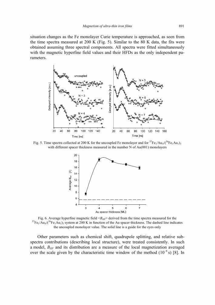
Magnetism of ultra-thin iron films 891
situation changes as the Fe monolayer Curie temperature is approached, as seen from the time spectra measured at 200 K (Fig. 5). Similar to the 80 K data, the fits were obtained assuming three spectral components. All spectra were fitted simultaneously with the magnetic hyperfine field values and their HFDs as the only independent pa-rameters.
Fig. 5. Time spectra collected at 200 K for the uncoupled Fe monolayer and for 57Fe1/AuN/(56Fe1Au1)3 with different spacer thickness measured in the number N of Au(001) monolayers
Fig. 6. Average hyperfine magnetic field <BHF> derived from the time spectra measured for the 57Fe1/AuN/(56Fe1Au1)3 system at 200 K in function of the Au spacer thickness. The dashed line indicates
the uncoupled monolayer value. The solid line is a guide for the eyes only
Other parameters such as chemical shift, quadrupole splitting, and relative sub-spectra contributions (describing local structure), were treated consistently. In such a model, BHF and its distribution are a measure of the local magnetization averaged over the scale given by the characteristic time window of the method (10–8 s) [8]. In
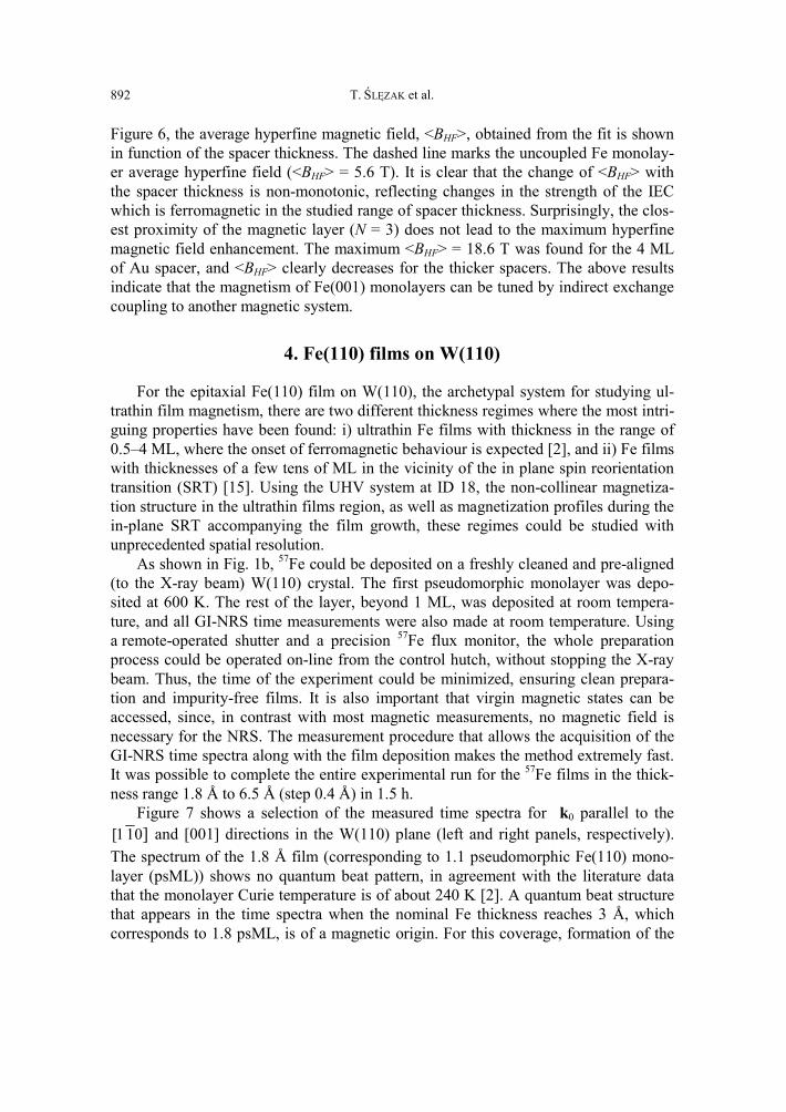
T. ŚLĘZAK et al. 892
Figure 6, the average hyperfine magnetic field, <BHF>, obtained from the fit is shown in function of the spacer thickness. The dashed line marks the uncoupled Fe monolay-er average hyperfine field (<BHF> = 5.6 T). It is clear that the change of <BHF> with the spacer thickness is non-monotonic, reflecting changes in the strength of the IEC which is ferromagnetic in the studied range of spacer thickness. Surprisingly, the clos-est proximity of the magnetic layer (N = 3) does not lead to the maximum hyperfine magnetic field enhancement. The maximum <BHF> = 18.6 T was found for the 4 ML of Au spacer, and <BHF> clearly decreases for the thicker spacers. The above results indicate that the magnetism of Fe(001) monolayers can be tuned by indirect exchange coupling to another magnetic system.
4. Fe(110) films on W(110)
For the epitaxial Fe(110) film on W(110), the archetypal system for studying ul-trathin film magnetism, there are two different thickness regimes where the most intri-guing properties have been found: i) ultrathin Fe films with thickness in the range of 0.5–4 ML, where the onset of ferromagnetic behaviour is expected [2], and ii) Fe films with thicknesses of a few tens of ML in the vicinity of the in plane spin reorientation transition (SRT) [15]. Using the UHV system at ID 18, the non-collinear magnetiza-tion structure in the ultrathin films region, as well as magnetization profiles during the in-plane SRT accompanying the film growth, these regimes could be studied with unprecedented spatial resolution.
As shown in Fig. 1b, 57Fe could be deposited on a freshly cleaned and pre-aligned (to the X-ray beam) W(110) crystal. The first pseudomorphic monolayer was depo-sited at 600 K. The rest of the layer, beyond 1 ML, was deposited at room tempera-ture, and all GI-NRS time measurements were also made at room temperature. Using a remote-operated shutter and a precision 57Fe flux monitor, the whole preparation process could be operated on-line from the control hutch, without stopping the X-ray beam. Thus, the time of the experiment could be minimized, ensuring clean prepara-tion and impurity-free films. It is also important that virgin magnetic states can be accessed, since, in contrast with most magnetic measurements, no magnetic field is necessary for the NRS. The measurement procedure that allows the acquisition of the GI-NRS time spectra along with the film deposition makes the method extremely fast. It was possible to complete the entire experimental run for the 57Fe films in the thick-ness range 1.8 Å to 6.5 Å (step 0.4 Å) in 1.5 h.
Figure 7 shows a selection of the measured time spectra for k0 parallel to the [1 10] and [001] directions in the W(110) plane (left and right panels, respectively). The spectrum of the 1.8 Å film (corresponding to 1.1 pseudomorphic Fe(110) mono-layer (psML)) shows no quantum beat pattern, in agreement with the literature data that the monolayer Curie temperature is of about 240 K [2]. A quantum beat structure that appears in the time spectra when the nominal Fe thickness reaches 3 Å, which corresponds to 1.8 psML, is of a magnetic origin. For this coverage, formation of the
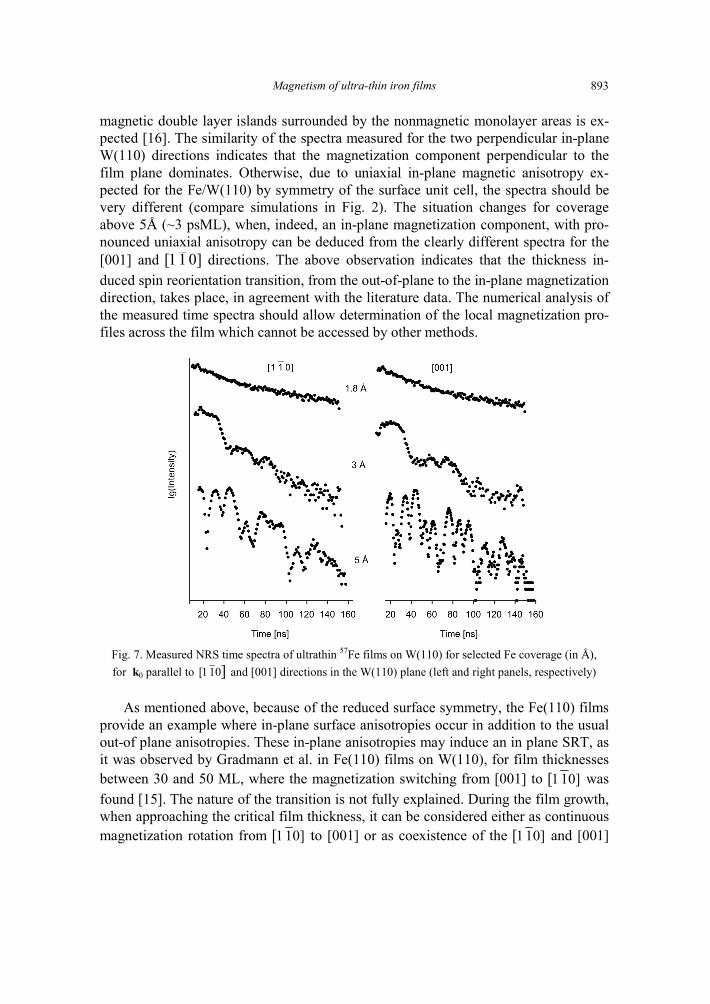
Magnetism of ultra-thin iron films 893
magnetic double layer islands surrounded by the nonmagnetic monolayer areas is ex-pected [16]. The similarity of the spectra measured for the two perpendicular in-plane W(110) directions indicates that the magnetization component perpendicular to the film plane dominates. Otherwise, due to uniaxial in-plane magnetic anisotropy ex-pected for the Fe/W(110) by symmetry of the surface unit cell, the spectra should be very different (compare simulations in Fig. 2). The situation changes for coverage above 5Å (~3 psML), when, indeed, an in-plane magnetization component, with pro-nounced uniaxial anisotropy can be deduced from the clearly different spectra for the [001] and ]011[ directions. The above observation indicates that the thickness in-duced spin reorientation transition, from the out-of-plane to the in-plane magnetization direction, takes place, in agreement with the literature data. The numerical analysis of the measured time spectra should allow determination of the local magnetization pro-files across the film which cannot be accessed by other methods.
Fig. 7. Measured NRS time spectra of ultrathin 57Fe films on W(110) for selected Fe coverage (in Å), for k0 parallel to [1 10] and [001] directions in the W(110) plane (left and right panels, respectively)
As mentioned above, because of the reduced surface symmetry, the Fe(110) films provide an example where in-plane surface anisotropies occur in addition to the usual out-of plane anisotropies. These in-plane anisotropies may induce an in plane SRT, as it was observed by Gradmann et al. in Fe(110) films on W(110), for film thicknesses between 30 and 50 ML, where the magnetization switching from [001] to 1 10][ was found [15]. The nature of the transition is not fully explained. During the film growth, when approaching the critical film thickness, it can be considered either as continuous magnetization rotation from 1 10][ to [001] or as coexistence of the 1 10][ and [001]
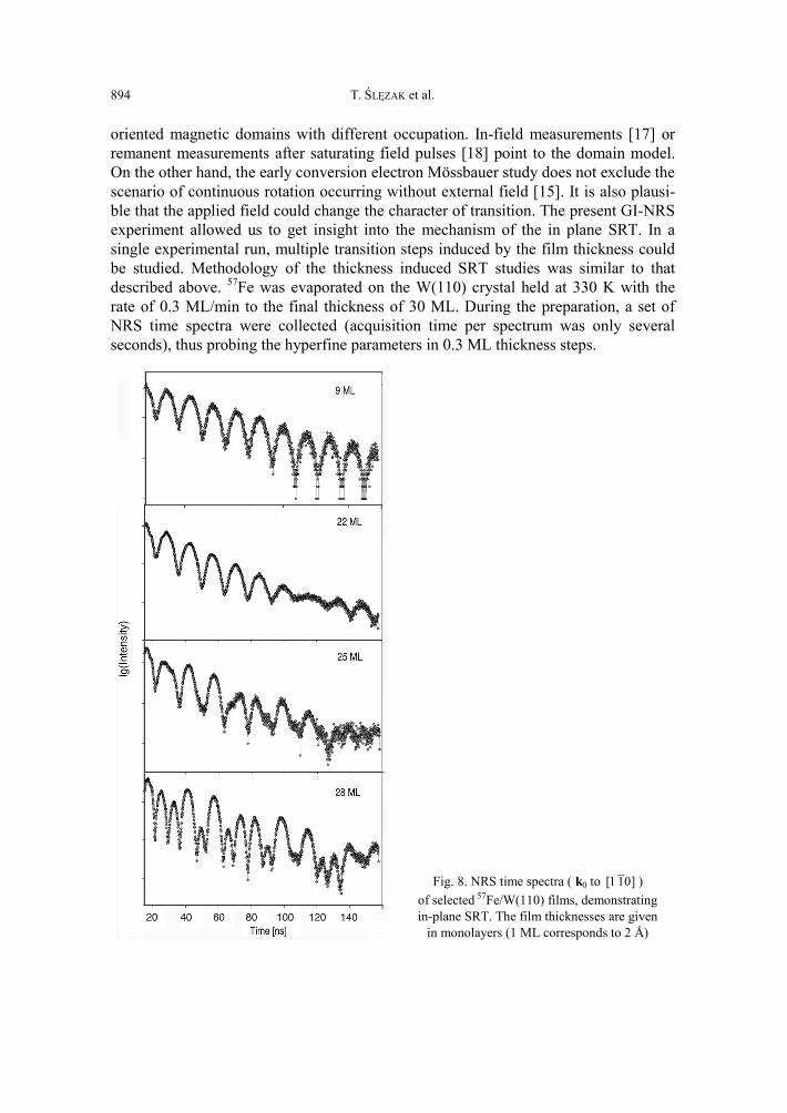
T. ŚLĘZAK et al. 894
oriented magnetic domains with different occupation. In-field measurements [17] or remanent measurements after saturating field pulses [18] point to the domain model. On the other hand, the early conversion electron Mössbauer study does not exclude the scenario of continuous rotation occurring without external field [15]. It is also plausi-ble that the applied field could change the character of transition. The present GI-NRS experiment allowed us to get insight into the mechanism of the in plane SRT. In a single experimental run, multiple transition steps induced by the film thickness could be studied. Methodology of the thickness induced SRT studies was similar to that described above. 57Fe was evaporated on the W(110) crystal held at 330 K with the rate of 0.3 ML/min to the final thickness of 30 ML. During the preparation, a set of NRS time spectra were collected (acquisition time per spectrum was only several seconds), thus probing the hyperfine parameters in 0.3 ML thickness steps.
Fig. 8. NRS time spectra ( k0 to [1 10] ) of selected 57Fe/W(110) films, demonstrating in-plane SRT. The film thicknesses are given
in monolayers (1 ML corresponds to 2 Å)
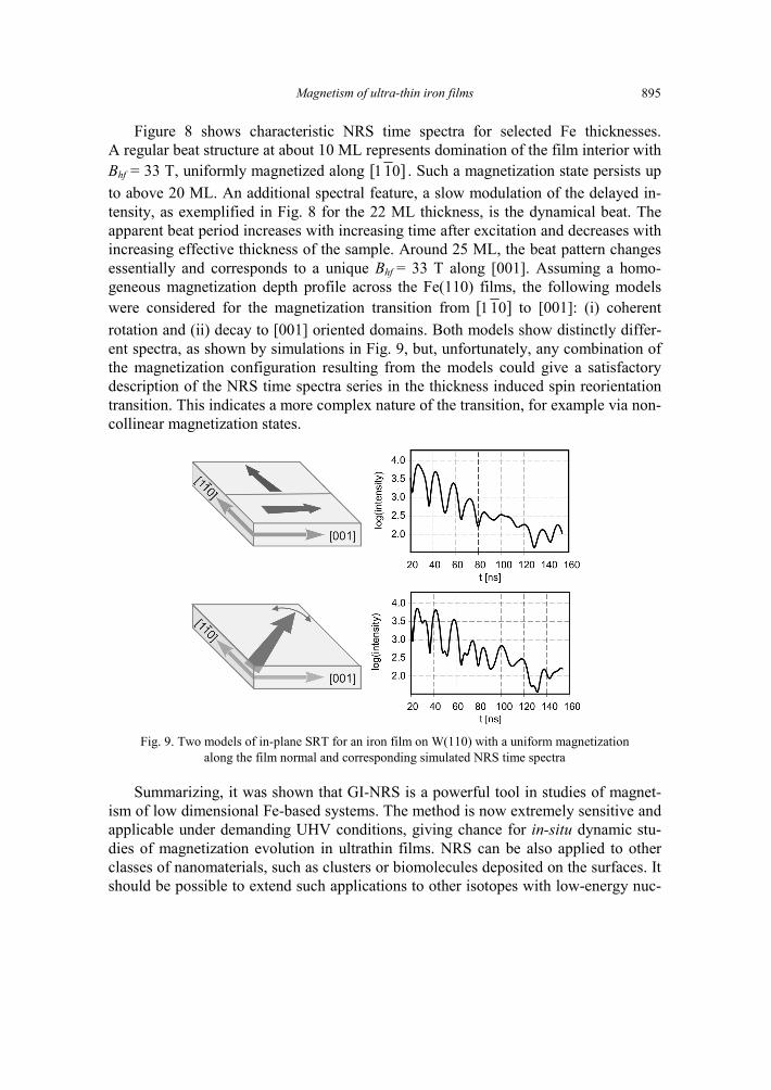
Magnetism of ultra-thin iron films 895
Figure 8 shows characteristic NRS time spectra for selected Fe thicknesses. A regular beat structure at about 10 ML represents domination of the film interior with Bhf = 33 T, uniformly magnetized along 1 10[ ] . Such a magnetization state persists up to above 20 ML. An additional spectral feature, a slow modulation of the delayed in-tensity, as exemplified in Fig. 8 for the 22 ML thickness, is the dynamical beat. The apparent beat period increases with increasing time after excitation and decreases with increasing effective thickness of the sample. Around 25 ML, the beat pattern changes essentially and corresponds to a unique Bhf = 33 T along [001]. Assuming a homo- geneous magnetization depth profile across the Fe(110) films, the following models were considered for the magnetization transition from 1 10[ ] to [001]: (i) coherent rotation and (ii) decay to [001] oriented domains. Both models show distinctly differ-ent spectra, as shown by simulations in Fig. 9, but, unfortunately, any combination of the magnetization configuration resulting from the models could give a satisfactory description of the NRS time spectra series in the thickness induced spin reorientation transition. This indicates a more complex nature of the transition, for example via non-collinear magnetization states.
Fig. 9. Two models of in-plane SRT for an iron film on W(110) with a uniform magnetization
along the film normal and corresponding simulated NRS time spectra
Summarizing, it was shown that GI-NRS is a powerful tool in studies of magnet-ism of low dimensional Fe-based systems. The method is now extremely sensitive and applicable under demanding UHV conditions, giving chance for in-situ dynamic stu-dies of magnetization evolution in ultrathin films. NRS can be also applied to other classes of nanomaterials, such as clusters or biomolecules deposited on the surfaces. It should be possible to extend such applications to other isotopes with low-energy nuc-
T. ŚLĘZAK et al. 896
lear transitions (below 30 keV), such as rare-earth isotopes 169Tm, 151Eu, 149Sm, and 161Dy, which are also of great interest for their magnetic properties.
Acknowledgements
This work was supported by the European Community under the Specific Targeted Research Project Contract No. NMP4-CT-2003-001516 (DYNASYNC), by the Austrian Federal Ministry of Education, Science and Culture under grant GZ 45.529/2-VI/B/7a/2002 (MDN project) and by the Polish Ministry of Education and Science. J.K. gratefully acknowledges professorial grant of the Foundation for Polish Science (FNP).
References
[1] PIETZSCH O., KUBETZKA A., BODE M., WIESENDANGER R., Phys. Rev. Lett., 84 (2000), 5212. [2] ELMERS H.J., HAUSCHILD J., HOCHE H., GRADMANN U., BETHGE H., HEUER D., KOHLER U., Phys.
Rev. Lett., 73 (1994), 898. [3]LU L., BANSMANN J., MEIWES-BROER K.H.J., Phys. Cond. Matter, 10 (1998), 2873. [4] ŚLĘZAK T., KARAŚ W., KROP K., KUBIK M., WILGOCKA-ŚLĘZAK D., SPIRIDIS N., KORECKI J., J. Magn.
Magn. Matter., 240 (2002), 362. [5] ELMERS H.J., HAUSCHILD J., GRADMANN U., Phys. Rev. B, 59 (1999), 3688. [6] PRZYBYLSKI M., KORECKI J., GRADMANN U., Appl. Phys. A, 52 (1991), 33 [7] Hyperfine Interact., 123/124 (1999), Issue on Nuclear Resonant Scattering of Synchrotron Radiation,
E. Gerdau, H. de Ward (Eds.); RÜFFER R., Hyperfine Interact. 141–142 (2002), 83. [8] RÖHLSBERGER R., Nuclear Condensed Matter Physics with Synchrotron Radiation, STMP 208,
Springer-Verlag, Berlin, 2004. [9] STANKOV S., RÜFFER R., SLADECEK M., RENNHOFER M., SEPIOŁ B., VOGL G., SPIRIDIS N., ŚLĘZAK T.,
KORECKI J., Rev. Sci. Instr., 79 (2008), 045108. [10] RÜFFER R., CHUMAKOV A.I., Hyperfine Interact. 97–98 (1996), 589; http://www.esrf.fr/exp_facilities/ID18/ [11] STURHAHN W., Hyperfine Interact. 125 (2000), 149. [12] RÖHLSBERGER R., BANSMANN J., SENZ V., JONAS K.L., BETTAC A., MEIWES-BROER K.H., LEUPOLD O.,
Phys. Rev. B, 67 (2003), 245412. [13] ŚLĘZAK T., ŚLĘZAK M., MATLAK K., ROHLSBERGER R., L’ABBE C., RÜFFER R., SPIRIDIS N., ZAJĄC M.,
KORECKI J., Surf. Sci., 601 (2007), 4300. [14] KARAŚ W., HANDKE B., KROP K., KUBIK M., ŚLĘZAK T., SPIRIDIS N., WILGOCKA-ŚLĘZAK D., KORECKI J.,
Phys. Stat. Sol. A, 189 (2002), 287 [15] GRADMANN U., KORECKI J., WALLER C., Appl. Phys. A, 39 (1986) 101. [16] WEBER N., WAGNER K., ELMERS H.J., HAUSCHILD J., GRADMANN U., Phys. Rev. B 55 (1997), 14121. [17] ELMERS H.J., GRADMANN U., Appl. Phys. A, 51 (1990), 255. [18] BAEK I.-G., LEE H.G., KIM H.-J., VESCOVO E., Phys. Rev. B, 67 (2003), 075401.
Received 16 May 2007
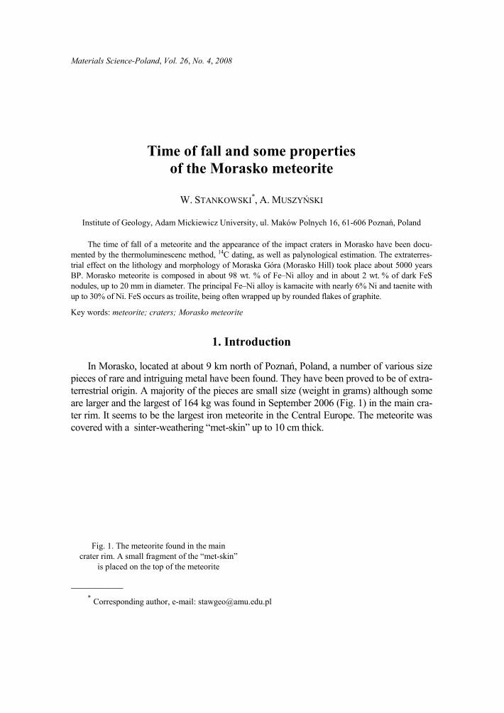
Materials Science-Poland, Vol. 26, No. 4, 2
Time of fallof the M
W. STANK
Institute of Geology, Adam Mickiewicz
The time of fall of a meteorite and themented by the thermoluminescenc method, trial effect on the lithology and morphologyBP. Morasko meteorite is composed in abonodules, up to 20 mm in diameter. The princup to 30% of Ni. FeS occurs as troilite, being
Key words: meteorite; craters; Morasko me
1
In Morasko, located at about 9 kpieces of rare and intriguing metal haterrestrial origin. A majority of the pare larger and the largest of 164 kg wter rim. It seems to be the largest ironcovered with a sinter-weathering “m
Fig. 1. The meteorite found in the macrater rim. A small fragment of the “met-
is placed on the top of the meteorite
__________ * Corresponding author, e-mail: stawg
2008
l and some properties Morasko meteorite
KOWSKI*, A. MUSZYŃSKI
University, ul. Maków Polnych 16, 61-606 Poznań, Poland
e appearance of the impact craters in Morasko have been docu14C dating, as well as palynological estimation. The extraterres
y of Moraska Góra (Morasko Hill) took place about 5000 yearout 98 wt. % of Fe–Ni alloy and in about 2 wt. % of dark Fecipal Fe–Ni alloy is kamacite with nearly 6% Ni and taenite witg often wrapped up by rounded flakes of graphite.
eteorite
. Introduction
km north of Poznań, Poland, a number of various sizave been found. They have been proved to be of extrapieces are small size (weight in grams) although somwas found in September 2006 (Fig. 1) in the main cran meteorite in the Central Europe. The meteorite wa
met-skin” up to 10 cm thick.
ain -skin” e
u-s-rs
eS th
ze a-
me a-as
W. STANKOWSKI, A. MUSZYŃSKI 898
In the period 1914–2006 almost 1000 kg of metallic extraterrestrial matter were recorded to have been found in the Morasko Meteorite Reserve and its surrounding. It is impossible to estimate how many of them were found and illegally introduced on international collector’s market. The known meteorite lumps were found directly on the topographic surface as well as below the surface, not deeper than about 20–80 cm. Theoretically, they can be integral components of glacigenic materials, incorporated in the ice cup in Scandinavia. Another possibility is the meteorite shower fall on the inland ice vaulting. After the ice movement and melting, the lumps were deposited in Morasko Quaternary deposits. Nevertheless the results of many years research proved the local fall of meteorites, thousands of years after Moraska Góra glacial morpho-genesis and permafrost degradation on this area. These lumps of iron are treated as an evidence of the largest European iron meteorite shower [1].
2. Time of fall and morphogenesis of craters
The Moraska Góra internal structure comprises deformed Neogene (a few million years of age) and Pleistocene deposits (the oldest one is older than 0.5 million years), its palaeomorphological rise is older than the last glaciation [2]. In the last Vistulian glaciation (~20000 BP) the shallow secondary glacitectonic deformations were formed. The degradation of the permafrost in Moraska Góra and around it occurred between 14 000 and 10 000 years BP. The erosive depressions and kettle-holes, pre-dominantly longitudinal and irregular in shape, were filled with organic deposits older than the Holocene one [3]. The age of the deepest organic infilling the thermocarst depressions is documented palynologiclly and by 14C dating.
Over a small area north-east of the Moraska Góra top, there are several very regu-lar oval depressions with circumferential ridges of various shapes. Their organic infill-ing are much younger than that typical of other, mainly cryogenic ones dated back to pre-Holocene time. According to Tobolski’s palynological estimations [5] and 14C data worked out at two laboratories: Gliwice Radioisotopes and Poznań Radiocarbon, organic accumulation in the Morasko Reserve depressions started not earlier than in the middle stage of the Atlantic period (Table 1). It seems to be an important indicator of the extraterrestrial origin of the depressions studied.
The conditions suitable for the development of organic sediments occurred in each depression at a different time. The oldest sediment was found in the deepest part of the crater B. In the shallower fragments of the depressions, sedimentation started much later. Very interesting are the data from crater E, where the organic materials devel-oped in two levels, divided by a gravitational accumulation of a mineral matter. The Morasko Reserve depressions make a conspicuous complex of meteorite craters.
Thousands of years after glacial morphogenesis and permafrost degradation, the meteorite shower fell into loose and loosely coherent materials, producing no impact breccias, high-pressure minerals nor glass. The impact is documented by meteorites, micrometeorites, iron spherules and shock-pressure structures. The date of the fall was
Time of fall and some properties of the Morasko meteorite 899
proved lately by the thermoluminescence (TL) technique applied to four meteorite “skin covers” – hard meteorite framing, produced as a consequence of fall of a very hot meteor-ite (zeroing of previous luminescence) and later weathering processes. The results of measurements are: 5.2±09 (UG-5941); 5.0±0.7 (UG-5941); 4.7±0.4 (UG-5943); 6.1± 0.7 (UG-5944). The new luminescence signal (101 OSL measurements resulted in 13% values < 5000 BP, 30% values < 10 000BP – totally 43% values < 10 000 BP) and age of craters organic infilling (radiometric dating [2, 4] and palynological estimation [5, 6]) provide convincing argument for the Morasko extraterrestrial event.
Table 1. Morasko craters. Radiometric data and palynological estimationa
Years BP Beginning of crater organic infilling
Palynological estimation [5, 6]
14C datings of craters in Gliwice and Poznań laboratories A B C E
0
5000–5500
260±80 690±95
640±90 690±150 990±160
610±75 650±110
2000 2690±170 3000 3360±100
4000 4465±35 4495±35 4760±40
10 000 Permafrost degradation not later than 10000 years BP [3]
a 14C data for mineral/organic boundary of different borings, elaborated by Pazdur (Gliwice) and Goslar (Poznań).
It should be added that below the plausible trajectory of the Morasko meteorite, at a site Szlaban near Oborniki situated ca. ~30 km north of Morasko, in the peat bog layer dated to 4750±40 (Poz-7004) – 5070±40 (Poz-7005) some parts rich in metallic sphereules were found [7]. Analysis of the available data has proved that the local impact of Morasko meteorite shower dates back to about 5000 years BP.
3. Mineralogical properties of meteorites
Morasko meteorite is composed in about 98 wt. % of (Fe–Ni)-alloy and in about 2 wt. % of dark FeS nodules, up to 20 mm in diameter (Figs. 1 and 3). The latter is the host of different trace minerals, which carry many trace elements.
The principal Fe–Ni minerals are kamacite with generally about 6% Ni and taenite with up to 30% Ni. FeS occurs as troilite, being often wrapped by rounded flakes of graphite (Figs. 3 and 4). Troilite is not known from Earth rocks, since pyrite, marcasite and pyrothine are dominant. Trace minerals in the troilite phase include schreibersite, cohenite, sphalerite, and graphite [8]. Additionally, tiny grains of daubreelite, altaite and silicate minerals were found, the latter being identified as the green Na-pyroxene cosmochlor (theoretically, NaCrSi2O6 [9]) and as feldspar. Most of these trace miner-als occur at the margins, but some within the troilite nodules (Fig. 43).
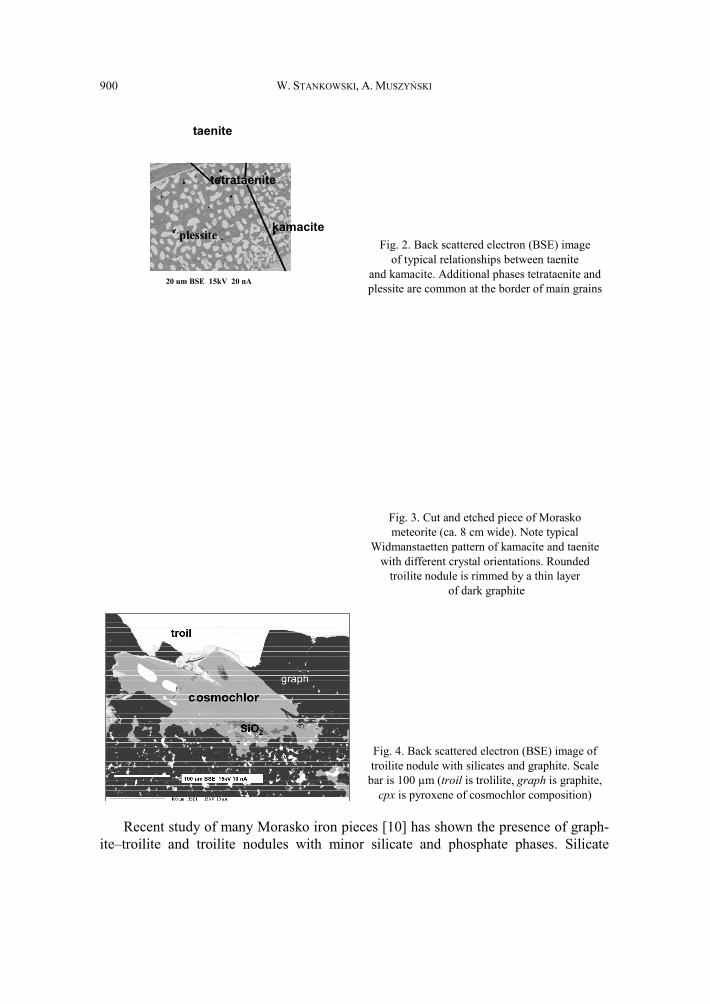
W. STA900
kamac
taenite
plessite
tetrataenite
20 um BSE 15kV 20 nA
Recent study of many Moraskoite–troilite and troilite nodules wi
ANKOWSKI, A. MUSZYŃSKI
cite
Fig. 2. Back scattered electron (BSE) image of typical relationships between taenite
and kamacite. Additional phases tetrataenite and plessite are common at the border of main grains
Fig. 3. Cut and etched piece of Morasko meteorite (ca. 8 cm wide). Note typical
Widmanstaetten pattern of kamacite and taenite with different crystal orientations. Rounded
troilite nodule is rimmed by a thin layer of dark graphite
Fig. 4. Back scattered electron (BSE) image of troilite nodule with silicates and graphite. Scale
bar is 100 μm (troil is trolilite, graph is graphite,cpx is pyroxene of cosmochlor composition)
o iron pieces [10] has shown the presence of graphith minor silicate and phosphate phases. Silicat
h-te
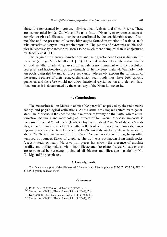
Time of fall and some properties of the Morasko meteorite 901
phases are represented by pyroxene, olivine, alkali feldspar and silica (Fig. 4). These are accompanied by Na, Ca, Mg and Fe phosphates. Diversity of pyroxenes suggests complex origins of silicates, a conjecture confirmed by the considerable share of cos-mochlor and the presence of cosmochlor–augite formed in reaction of residual melt with enstatite and crystallizes within chromite. The genesis of pyroxenes within nod-ules in Morasko type meteorites seems to be much more complex than is conjectured by Benedix et al. [11].
The origin of this group Fe-meteorites and their genetic conditions is discussed in literature (cf. e.g., Mittlefehldt et al. [12]). The condensation of extraterrestrial matter to solid metallic or silicate phases from nebula is not consistent with the exsolution processes and fractionations of the elements in the meteoric material. Similarly, mol-ten pools generated by impact processes cannot adequately explain the formation of the irons. Because of their reduced dimension such pools must have been quickly quenched and therefore would not allow fractional crystallization and element frac-tionation, as it is documented by the chemistry of the Morasko meteorite.
4. Conclusions
The meteorites fell in Morasko about 5000 years BP as proved by the radiometric datings and palynological estimations. At the same time impact craters were gener-ated. The Morasko is the specific site, one of ten to twenty on the Earth, where extra-terrestrial materials and morphological effects of fall occur. Morasko meteorite is composed in about 98 wt. % of (Fe–Ni) alloy and in about 2 wt. % of dark FeS nod-ules, up to 20 mm in diameter. The latter is the host of different trace minerals, carry-ing many trace elements. The principal Fe-Ni minerals are kamacite with generally about 6% Ni and taenite with up to 30% of Ni. FeS occurs as troilite, being often wrapped by rounded flakes of graphite. The trolilte is not known from Earth rocks. A recent study of many Morasko iron pieces has shown the presence of graphite –troilite and troilite nodules with minor silicate and phosphate phases. Silicate phases are represented by pyroxene, olivine, alkali feldspar and silica, accompanied by Na, Ca, Mg and Fe phosphates.
Acknowledgements
The financial support of the Ministry of Education and Science projects N N307 3533 33; 3P04E 004 25 is greatly acknowledged.
References
[1] PILSKI A.S., WALTON W., Meteorite, 5 (1999), 27. [2] STANKOWSKI W.T.J., Planet. Space Sci., 49 (2001), 749. [3] KOZARSKI S., Bad. Fizj. Polska Zach., 11, 14 (1963), 51. [4] STANKOWSKI W.T.J., Planet. Space Sci., 55 (2007), 871.
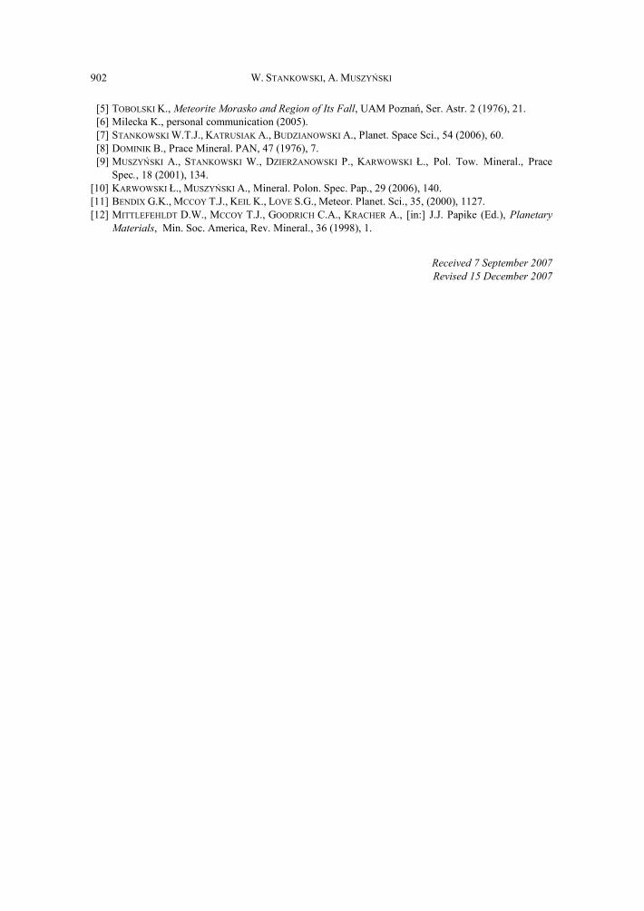
W. STANKOWSKI, A. MUSZYŃSKI 902
[5] TOBOLSKI K., Meteorite Morasko and Region of Its Fall, UAM Poznań, Ser. Astr. 2 (1976), 21. [6] Milecka K., personal communication (2005). [7] STANKOWSKI W.T.J., KATRUSIAK A., BUDZIANOWSKI A., Planet. Space Sci., 54 (2006), 60. [8] DOMINIK B., Prace Mineral. PAN, 47 (1976), 7. [9] MUSZYŃSKI A., STANKOWSKI W., DZIERŻANOWSKI P., KARWOWSKI Ł., Pol. Tow. Mineral., Prace
Spec., 18 (2001), 134. [10] KARWOWSKI Ł., MUSZYŃSKI A., Mineral. Polon. Spec. Pap., 29 (2006), 140. [11] BENDIX G.K., MCCOY T.J., KEIL K., LOVE S.G., Meteor. Planet. Sci., 35, (2000), 1127. [12] MITTLEFEHLDT D.W., MCCOY T.J., GOODRICH C.A., KRACHER A., [in:] J.J. Papike (Ed.), Planetary
Materials, Min. Soc. America, Rev. Mineral., 36 (1998), 1.
Received 7 September 2007 Revised 15 December 2007
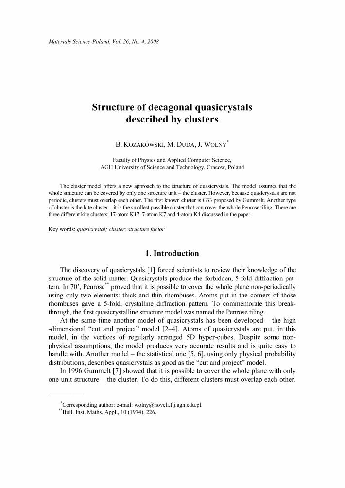
Materials Science-Poland, Vol. 26, No. 4, 2008
Structure of decagonal quasicrystals described by clusters
B. KOZAKOWSKI, M. DUDA, J. WOLNY*
Faculty of Physics and Applied Computer Science, AGH University of Science and Technology, Cracow, Poland
The cluster model offers a new approach to the structure of quasicrystals. The model assumes that the whole structure can be covered by only one structure unit – the cluster. However, because quasicrystals are not periodic, clusters must overlap each other. The first known cluster is G33 proposed by Gummelt. Another type of cluster is the kite cluster – it is the smallest possible cluster that can cover the whole Penrose tiling. There are three different kite clusters: 17-atom K17, 7-atom K7 and 4-atom K4 discussed in the paper.
Key words: quasicrystal; cluster; structure factor
1. Introduction
The discovery of quasicrystals [1] forced scientists to review their knowledge of the structure of the solid matter. Quasicrystals produce the forbidden, 5-fold diffraction pat-tern. In 70’, Penrose** proved that it is possible to cover the whole plane non-periodically using only two elements: thick and thin rhombuses. Atoms put in the corners of those rhombuses gave a 5-fold, crystalline diffraction pattern. To commemorate this break-through, the first quasicrystalline structure model was named the Penrose tiling.
At the same time another model of quasicrystals has been developed – the high -dimensional “cut and project” model [2–4]. Atoms of quasicrystals are put, in this model, in the vertices of regularly arranged 5D hyper-cubes. Despite some non-physical assumptions, the model produces very accurate results and is quite easy to handle with. Another model – the statistical one [5, 6], using only physical probability distributions, describes quasicrystals as good as the “cut and project” model.
In 1996 Gummelt [7] showed that it is possible to cover the whole plane with only one unit structure – the cluster. To do this, different clusters must overlap each other. __________
*Corresponding author: e-mail: [email protected]. **Bull. Inst. Maths. Appl., 10 (1974), 226.
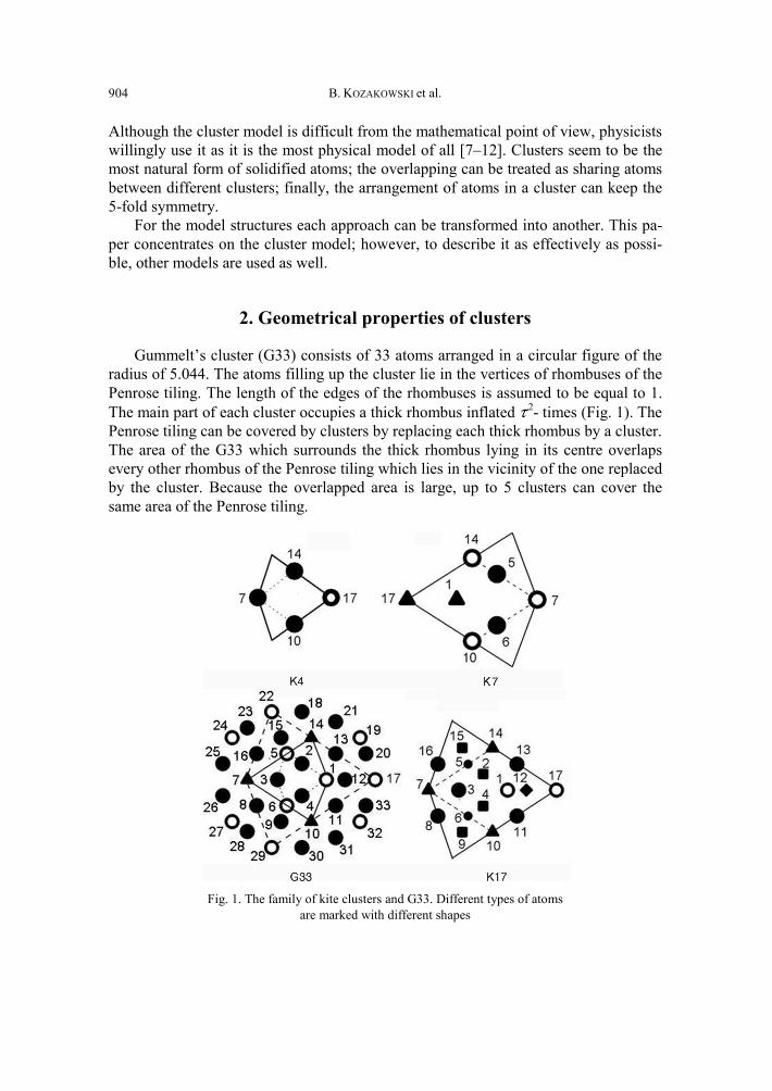
B. KOZAKOWSKI et al. 904
Although the cluster model is difficult from the mathematical point of view, physicists willingly use it as it is the most physical model of all [7–12]. Clusters seem to be the most natural form of solidified atoms; the overlapping can be treated as sharing atoms between different clusters; finally, the arrangement of atoms in a cluster can keep the 5-fold symmetry.
For the model structures each approach can be transformed into another. This pa-per concentrates on the cluster model; however, to describe it as effectively as possi-ble, other models are used as well.
2. Geometrical properties of clusters
Gummelt’s cluster (G33) consists of 33 atoms arranged in a circular figure of the radius of 5.044. The atoms filling up the cluster lie in the vertices of rhombuses of the Penrose tiling. The length of the edges of the rhombuses is assumed to be equal to 1. The main part of each cluster occupies a thick rhombus inflated τ 2- times (Fig. 1). The Penrose tiling can be covered by clusters by replacing each thick rhombus by a cluster. The area of the G33 which surrounds the thick rhombus lying in its centre overlaps every other rhombus of the Penrose tiling which lies in the vicinity of the one replaced by the cluster. Because the overlapped area is large, up to 5 clusters can cover the same area of the Penrose tiling.
Fig. 1. The family of kite clusters and G33. Different types of atoms are marked with different shapes
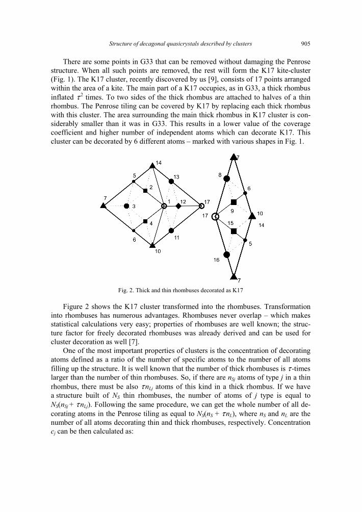
Structure of decagonal quasicrystals described by clusters 905
There are some points in G33 that can be removed without damaging the Penrose structure. When all such points are removed, the rest will form the K17 kite-cluster (Fig. 1). The K17 cluster, recently discovered by us [9], consists of 17 points arranged within the area of a kite. The main part of a K17 occupies, as in G33, a thick rhombus inflated τ 2 times. To two sides of the thick rhombus are attached to halves of a thin rhombus. The Penrose tiling can be covered by K17 by replacing each thick rhombus with this cluster. The area surrounding the main thick rhombus in K17 cluster is con-siderably smaller than it was in G33. This results in a lower value of the coverage coefficient and higher number of independent atoms which can decorate K17. This cluster can be decorated by 6 different atoms – marked with various shapes in Fig. 1.
Fig. 2. Thick and thin rhombuses decorated as K17
Figure 2 shows the K17 cluster transformed into the rhombuses. Transformation into rhombuses has numerous advantages. Rhombuses never overlap – which makes statistical calculations very easy; properties of rhombuses are well known; the struc-ture factor for freely decorated rhombuses was already derived and can be used for cluster decoration as well [7].
One of the most important properties of clusters is the concentration of decorating atoms defined as a ratio of the number of specific atoms to the number of all atoms filling up the structure. It is well known that the number of thick rhombuses is τ -times larger than the number of thin rhombuses. So, if there are nSj atoms of type j in a thin rhombus, there must be also τnLj atoms of this kind in a thick rhombus. If we have a structure built of NS thin rhombuses, the number of atoms of j type is equal to NS(nSj + τnLj). Following the same procedure, we can get the whole number of all de-corating atoms in the Penrose tiling as equal to NS(nS + τnL), where nS and nL are the number of all atoms decorating thin and thick rhombuses, respectively. Concentration cj can be then calculated as:
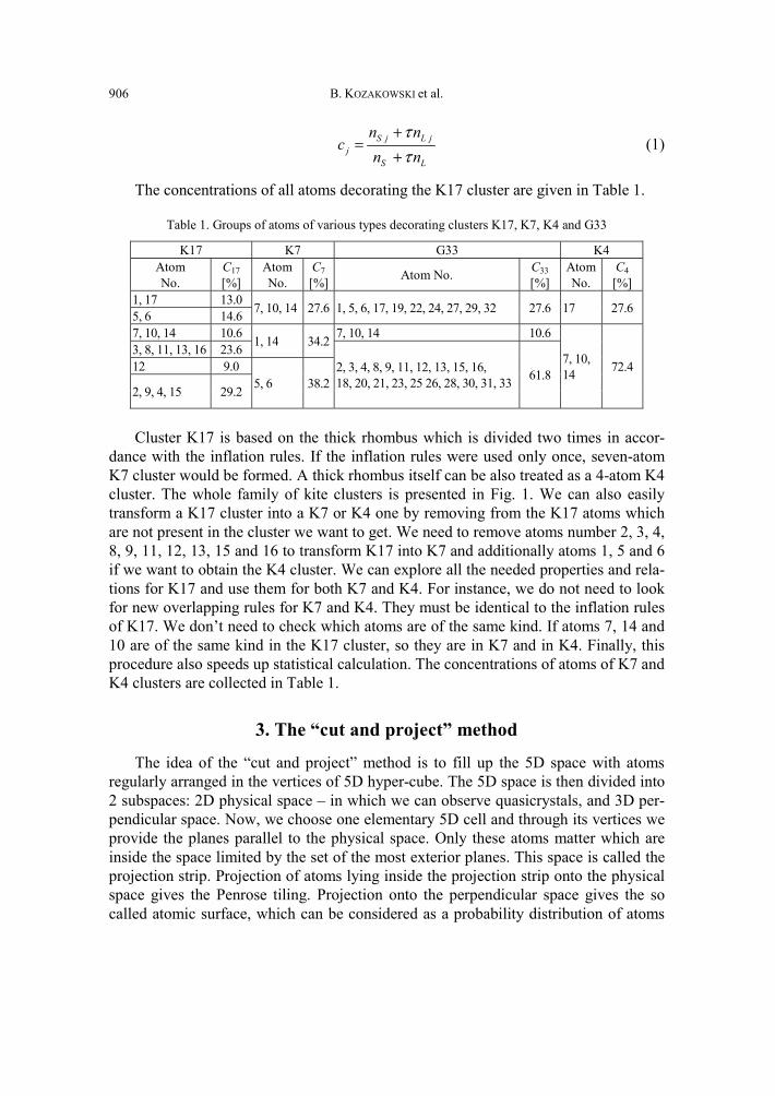
B. KOZAKOWSKI et al. 906
S j L jj
S L
n nc
n nττ
+=
+ (1)
The concentrations of all atoms decorating the K17 cluster are given in Table 1.
Table 1. Groups of atoms of various types decorating clusters K17, K7, K4 and G33
K17 K7 G33 K4 Atom No.
C17 [%]
Atom No.
C7 [%] Atom No. C33
[%] AtomNo.
C4 [%]
1, 17 13.0 7, 10, 14 27.6 1, 5, 6, 17, 19, 22, 24, 27, 29, 32 27.6 17 27.6 5, 6 14.6 7, 10, 14 10.6 1, 14 34.2 7, 10, 14 10.6
7, 10, 14 72.4
3, 8, 11, 13, 16 23.6 2, 3, 4, 8, 9, 11, 12, 13, 15, 16, 18, 20, 21, 23, 25 26, 28, 30, 31, 33 61.8
12 9.0 5, 6 38.2 2, 9, 4, 15 29.2
Cluster K17 is based on the thick rhombus which is divided two times in accor-
dance with the inflation rules. If the inflation rules were used only once, seven-atom K7 cluster would be formed. A thick rhombus itself can be also treated as a 4-atom K4 cluster. The whole family of kite clusters is presented in Fig. 1. We can also easily transform a K17 cluster into a K7 or K4 one by removing from the K17 atoms which are not present in the cluster we want to get. We need to remove atoms number 2, 3, 4, 8, 9, 11, 12, 13, 15 and 16 to transform K17 into K7 and additionally atoms 1, 5 and 6 if we want to obtain the K4 cluster. We can explore all the needed properties and rela-tions for K17 and use them for both K7 and K4. For instance, we do not need to look for new overlapping rules for K7 and K4. They must be identical to the inflation rules of K17. We don’t need to check which atoms are of the same kind. If atoms 7, 14 and 10 are of the same kind in the K17 cluster, so they are in K7 and in K4. Finally, this procedure also speeds up statistical calculation. The concentrations of atoms of K7 and K4 clusters are collected in Table 1.
3. The “cut and project” method
The idea of the “cut and project” method is to fill up the 5D space with atoms regularly arranged in the vertices of 5D hyper-cube. The 5D space is then divided into 2 subspaces: 2D physical space – in which we can observe quasicrystals, and 3D per-pendicular space. Now, we choose one elementary 5D cell and through its vertices we provide the planes parallel to the physical space. Only these atoms matter which are inside the space limited by the set of the most exterior planes. This space is called the projection strip. Projection of atoms lying inside the projection strip onto the physical space gives the Penrose tiling. Projection onto the perpendicular space gives the so called atomic surface, which can be considered as a probability distribution of atoms
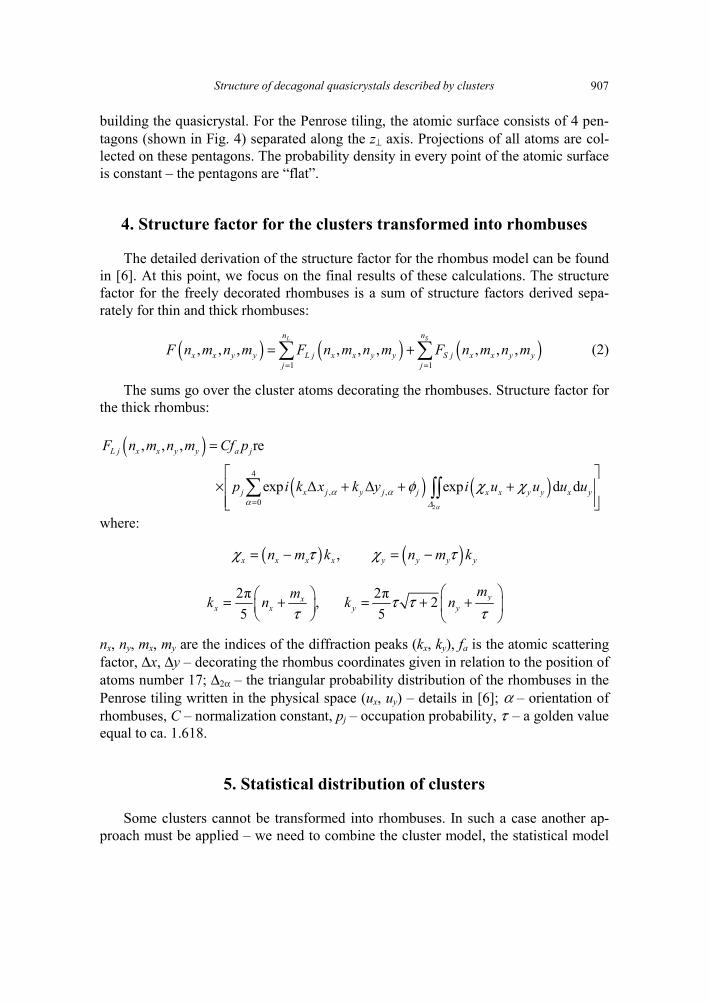
Structure of decagonal quasicrystals described by clusters 907
building the quasicrystal. For the Penrose tiling, the atomic surface consists of 4 pen-tagons (shown in Fig. 4) separated along the z⊥ axis. Projections of all atoms are col-lected on these pentagons. The probability density in every point of the atomic surface is constant – the pentagons are “flat”.
4. Structure factor for the clusters transformed into rhombuses
The detailed derivation of the structure factor for the rhombus model can be found in [6]. At this point, we focus on the final results of these calculations. The structure factor for the freely decorated rhombuses is a sum of structure factors derived sepa-rately for thin and thick rhombuses:
( ) ( ) ( )1 1
, , , , , , , , ,SL nn
x x y y L j x x y y S j x x y yj j
F n m n m F n m n m F n m n m= =
= +∑ ∑ (2)
The sums go over the cluster atoms decorating the rhombuses. Structure factor for the thick rhombus:
( )
( ) ( )2
4
, ,0
, , , re
exp Δ Δ exp d d
L j x x y y a j
j x j y j j x x y y x y
F n m n m Cf p
p i k x k y i u u u uα
α αα Δ
φ χ χ=
=
⎡ ⎤× + + +⎢ ⎥⎢ ⎥⎣ ⎦∑ ∫∫
where:
( ) ,x x x xn m kχ τ= − ( )y y y yn m kχ τ= −
2π 2π, 25 5
yxx x y y
mmk n k nτ ττ τ
⎛ ⎞⎛ ⎞= + = + +⎜ ⎟⎜ ⎟⎝ ⎠ ⎝ ⎠
nx, ny, mx, my are the indices of the diffraction peaks (kx, ky), fa is the atomic scattering factor, Δx, Δy – decorating the rhombus coordinates given in relation to the position of atoms number 17; Δ2α – the triangular probability distribution of the rhombuses in the Penrose tiling written in the physical space (ux, uy) – details in [6]; α – orientation of rhombuses, C – normalization constant, pj – occupation probability, τ – a golden value equal to ca. 1.618.
5. Statistical distribution of clusters
Some clusters cannot be transformed into rhombuses. In such a case another ap-proach must be applied – we need to combine the cluster model, the statistical model
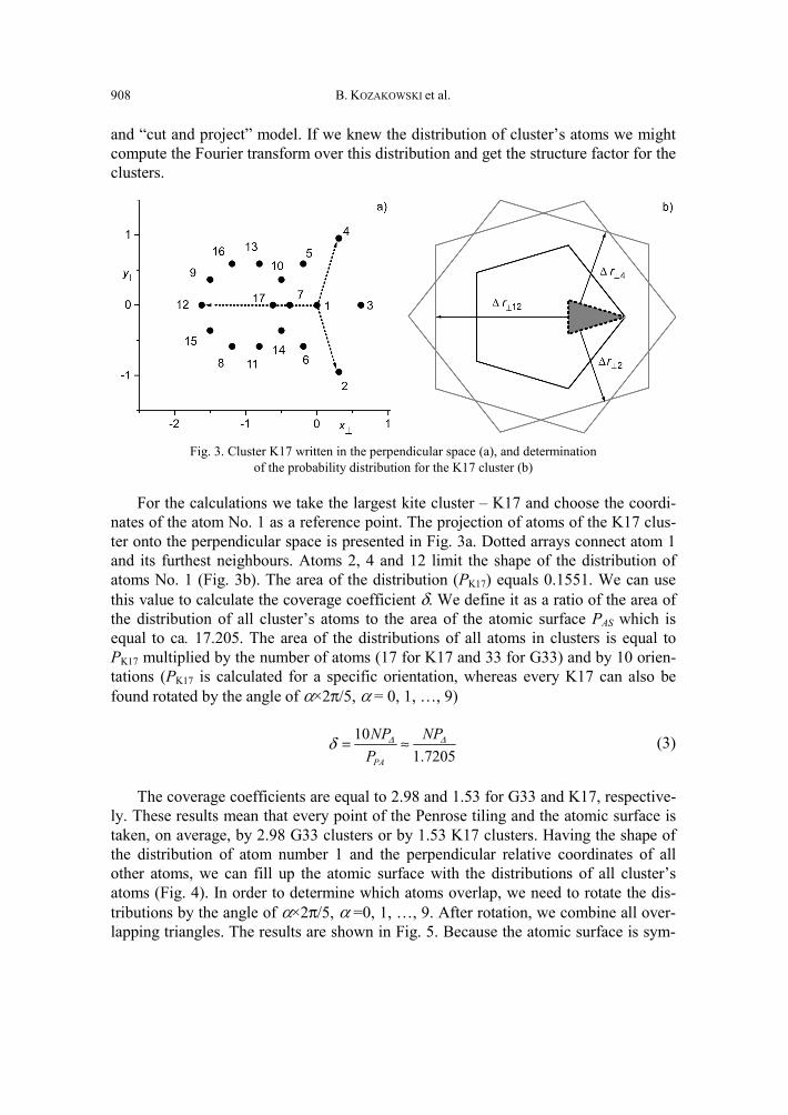
B. KOZAKOWSKI et al. 908
and “cut and project” model. If we knew the distribution of cluster’s atoms we might compute the Fourier transform over this distribution and get the structure factor for the clusters.
Fig. 3. Cluster K17 written in the perpendicular space (a), and determination of the probability distribution for the K17 cluster (b)
For the calculations we take the largest kite cluster – K17 and choose the coordi-nates of the atom No. 1 as a reference point. The projection of atoms of the K17 clus-ter onto the perpendicular space is presented in Fig. 3a. Dotted arrays connect atom 1 and its furthest neighbours. Atoms 2, 4 and 12 limit the shape of the distribution of atoms No. 1 (Fig. 3b). The area of the distribution (PK17) equals 0.1551. We can use this value to calculate the coverage coefficient δ. We define it as a ratio of the area of the distribution of all cluster’s atoms to the area of the atomic surface PAS which is equal to ca. 17.205. The area of the distributions of all atoms in clusters is equal to PK17 multiplied by the number of atoms (17 for K17 and 33 for G33) and by 10 orien-tations (PK17 is calculated for a specific orientation, whereas every K17 can also be found rotated by the angle of α×2π/5, α = 0, 1, …, 9)
101.7205PA
NP NPP
Δ Δδ = ≈ (3)
The coverage coefficients are equal to 2.98 and 1.53 for G33 and K17, respective-ly. These results mean that every point of the Penrose tiling and the atomic surface is taken, on average, by 2.98 G33 clusters or by 1.53 K17 clusters. Having the shape of the distribution of atom number 1 and the perpendicular relative coordinates of all other atoms, we can fill up the atomic surface with the distributions of all cluster’s atoms (Fig. 4). In order to determine which atoms overlap, we need to rotate the dis-tributions by the angle of α×2π/5, α =0, 1, …, 9. After rotation, we combine all over-lapping triangles. The results are shown in Fig. 5. Because the atomic surface is sym-
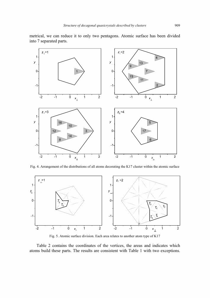
Structure of decagonal quasicrystals described by clusters 909
metrical, we can reduce it to only two pentagons. Atomic surface has been divided into 7 separated parts.
Fig. 4. Arrangement of the distributions of all atoms decorating the K17 cluster within the atomic surface
Fig. 5. Atomic surface division. Each area relates to another atom type of K17
Table 2 contains the coordinates of the vertices, the areas and indicates which atoms build these parts. The results are consistent with Table 1 with two exceptions.
B. KOZAKOWSKI et al. 910
There are two more independent types of atom in Table 2 when compared with Ta-ble 1. Atoms 2 plus 9 never overlap 4 plus 15. Their positions in clusters are symme-trical and because of that we assume that they must be of the same kind. Additionally, atoms 1 and 17 are separated, because their triangle distributions do not overlap – they don’t need to be of the same kind. This is the major difference between the cluster and rhombus models. In the rhombus model we had to assume these two atoms to be equal. The source of this difference lies in the empty vertices of kite clusters. When we transform clusters into the rhombuses we have to put atom number 17 into these vacant spots.
Table 2. Numerical description of the atomic surface divided into separated parts assigned to various types of atoms decorating the K17 cluster
Atom No. Vertex 1 Vertex 2 Vertex 3 Area Concentration
C17 [%] T1A 1 0, 0 2⋅(2 – τ ), 0 2τ – 3, τ – 2 0.069 13 T1B 17 τ , 1 – τ 2(2 – τ ), 0 2τ – 3, τ – 2 0.155T2 5, 6 2(2 – τ ), 0 τ , τ – 1 τ , 1 – τ 0.251 14.6 T3 7, 10, 14 0, 0 2(τ – 1), 0 2 – τ , 1 – τ 0.182 10.6 T4 3, 8, 11, 13, 16 τ + 1, – 1 2(τ – 1), 0 2 – τ , 1 – τ 0.406 23.6 T5 12 2 – τ , 1 – τ 2 – τ , τ – 3 2(τ – 1), 2(1 – τ ) 0.155 9.0 T6 2, 9 2 – τ , 1 – τ τ + 1, – 1 2(τ – 1), 2(1 – τ ) 0.251 14.6 T7 4, 15 2(τ – 1), 0 τ + 1, 3 – 2τ τ + 1, –1 0.251 14.6
The area of each separated part of the atomic surface is proportional to the number
of atoms belonging to the area. This gives us another opportunity for calculating the concentration of each atom – as a ratio of the area of a specific j atom Pj to the area of the atomic surface: cj = Pj/PAS. This equation leads to the results which are consistent with ones got by means of equation (1) – compare tables 1 and 2.
6. Structure factor for the cluster model
Having the atomic surface divided into the separated parts connected to different types of atoms we can calculate the Fourier transform over each of these parts. As a result we get a structure factor for the cluster model.
( ) ( ) ( )⎥⎥⎦
⎤
⎢⎢⎣
⎡+⋅= ∑ ∑ ∑ ∫∫
= = =
max
,,1
2
1
4
0, ddiexpiexpre,
t
t j Tyxyyxxjatyx
jt
uuuufCFα α
χχϕχχ (4)
The meaning of symbols used in this equation is described in Section 4. Equation (4) gives much less flexibility than (2). It should be used when a transformation into rhombuses is not possible.
Structure of decagonal quasicrystals described by clusters 911
7. Conclusions
The cluster model offers a new approach to the structure of quasicrystals. The model assumes that the whole structure can be covered by only one structure unit – the cluster. However, because quasicrystals are not periodic, clusters must overlap each other.
This model is more and more popular among the physicists. It gives a simple unit structure which can hold the symmetry of the diffraction pattern. Cluster is also more stable than rhombus form from the energetic point of view.
The first known cluster is G33 proposed by Petra Gummelt [7]. Another type of cluster is the kite cluster – it is the smallest possible cluster that can cover the whole Penrose tiling. There are three different kite clusters: 17-atom K17, 7-atom K7 and 4-atom K4.
The most important property of any cluster is the number of independent atoms that can decorate this cluster. In case of G33, there are 3 independent atoms which cover the plane with the relative concentration 62:28:11. In the case of kite clusters we have 6 independent atoms in K17 (29:24:15:13:11:9), 3 in K7 (38:34:28) and 2 in K4 (76:24). The relative concentration of atoms filling-up the kite-clusters is similar to the relative concentration of the atoms building the quasicrystalline stable compounds, for instance: composition of Al71TM29 [13, 14] versus (38 + 34):28 in the K7. Kite-clusters can be then used as a very good initial model for the further refinement. An-other important property of clusters is the value of the coverage coefficient. The higher value it has, the more intensively clusters overlap which has an effect on the number of independent atoms. Application of kite-clusters to the real decagonal quasi-crystals has been already proved and will be presented elsewhere [15].
To get some valuable theoretical properties of clusters we can transform them into rhombuses or use the “cut and project” method. Both methods impose their own limi-tation on clusters. The “cut and project” method allows decorating only in Penrose’s positions, the rhombus method not always can be used – some clusters cannot be transformed into rhombuses.
Acknowledgements
This work has been partially supported by CMA-NoE.
References
[1] SHECHTMAN D., BLECH I., GRATIAS D., CAHN J.W., Phys. Rev. Lett., 53 (1984), 1951. [2] DE BRUIJN N.G., Proc. K. Ned. Akad. Wet. Ser. A, 43 (1981), 39. [3] KRAMER P., NERI R., Acta Cryst., A 40 (1984), 580. [4] ELSER V., Phys. Rev. B, 31 (1985), 4892. [5] WOLNY J., Phil. Mag. A, 77 (1998), 395. [6] KOZAKOWSKI B., WOLNY J., Phil. Mag., 86 (2006), 549. [7] GUMMELT P., Geometriae Dedicata, 62 (1996), 1.

B. KOZAKOWSKI et al. 912
[8] STEINHARDT P.J., JEONG H.-C., Nature, 382 (1996), 433. [9] DĄBROWSKA A., KOZAKOWSKI B., WOLNY J., Acta Cryst., A61 (2005), 350. [10] GRATIAS D., PUYRAIMOND F., QUIQUANDOM M., Phys. Rev. B, 63 (2000), 1. [11] PAPADOPOLOS Z., KRASNER G., Ferroelectrics, 250 (2001), 409. [12] DUDA M., KOZAKOWSKI B., WOLNY J., J. Non-Cryst. Solids, 357 (2007), 2500. [13] TAKAKURA, H., YAMAMOTO A., TSAI A.P, Acta Cryst. A, 57 (2001), 576. [14] CERVELLINO A., HAIBACH T., STEURER W., Acta Cryst. B, 58 (2002), 8. [15] WOLNY J., KOZAKOWSKI B., DUDA M., LABNO B., ADAMOWSKI J., Decoration of inflated kite-
clusters, Phil. Mag., (2008), in print.
Received 7 September 2007 Revised 15 December 2007
Materials Science-Poland, Vol. 26, No. 4, 2008
Fracton mediated superconductivity in the “net fractal”systems. Preliminaries and
an overview of other fracton based models
Z. BĄK*
1Institute of Physics, JD University of Częstochowa, al. Armii Krajowej 13/15, Częstochowa 42-201, Poland
Assuming that the force constants scale as σ(λx) = λ–ασ(x), we construct the model of elastic (linear) excitations on a fractal (fractons). We show that the fractons on a specific class of fractals, “net fractals”, can be assumed to be log-scale phonons. Further, we discuss the model of fracton mediated superconduc-tivity in the “net fractal” systems). We show that with the use of logarithmic coordinates, the fracton mediated superconductivity can be described within a model which is reminiscent of the conventional BCS formulation.
Key words: fractals; fractons; superconductivity
1. Introduction
The concept of fractal geometry has proven useful in describing structures and processes in nanoscale many-body systems [1]. The hallmark of a fractality is a hie-rarchical organization of its elements, described by discrete scaling laws, which makes the fractal, regardless the magnification or contraction scale, look the same. This prop-erty of fractals is called self-similarity, self-affinity or self-replicability. Although physical systems modellled by fractals are non-translation invariant, it is well known fact that self-similar fractals as well as physical quantities on fractal systems show log -periodicities [1]. This opens a possibility to describe the symmetries of self-similar fractals (with the use of logarithmic scale), in a way that is reminiscent of convention-al formalism developed for crystalline systems [2]. Motivated by this fact, we present study of superconductivity, when the electron pairing is mediated by fractal excita-tions (fractons) [3].
__________
*E-mail: [email protected]
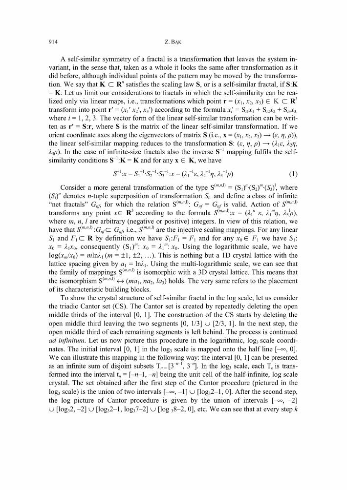
Z. BĄK
914
A self-similar symmetry of a fractal is a transformation that leaves the system in-variant, in the sense that, taken as a whole it looks the same after transformation as it did before, although individual points of the pattern may be moved by the transforma-tion. We say that K ⊂ Rn satisfies the scaling law S, or is a self-similar fractal, if S:K = K. Let us limit our considerations to fractals in which the self-similarity can be rea-lized only via linear maps, i.e., transformations which point r = (x1, x2, x3) ∈ K ⊂ R3
transform into point r′ = (x1′ x2′, x3′) according to the formula xi' = Si1x1 + Si2x2 + Si3x3; where i = 1, 2, 3. The vector form of the linear self-similar transformation can be writ-ten as r′ = S:r, where S is the matrix of the linear self-similar transformation. If we orient coordinate axes along the eigenvectors of matrix S (i.e., x = (x1, x2, x3) → (ε, η, ρ)), the linear self-similar mapping reduces to the transformation S: (ε, η, ρ) → (λ1ε, λ2η, λ3ρ). In the case of infinite-size fractals also the inverse S–1 mapping fulfils the self-similarity conditions S–1:K = K and for any x ∈ K, we have
S–1:x = S1–1·S2
–1·S3–1:x = (λ1
–1ε, λ2–1η, λ3
–1ρ) (1)
Consider a more general transformation of the type S(m,n,l) = (S1)n·(S2)m·(S3)l, where (Si)n denotes n-tuple superposition of transformation Si, and define a class of infinite “net fractals” Gnf, for which the relation S(m,n,l): Gnf = Gnf is valid. Action of S(m,n,l) transforms any point x∈ R3 according to the formula S(m,n,l):x = (λ1
n ε, λ1mη, λ3
lρ), where m, n, l are arbitrary (negative or positive) integers. In view of this relation, we have that S(m,n,l) :Gnf⊂ Gnf, i.e., S(m,n,l) are the injective scaling mappings. For any linear S1 and F1⊂ R by definition we have S1:F1 = F1 and for any x0 ∈ F1 we have S1: x0 = λ1x0, consequently (S1)m: x0 = λ1
m: x0. Using the logarithmic scale, we have log(xm/x0) = mlnλ1 (m = ±1, ±2, …). This is nothing but a 1D crystal lattice with the lattice spacing given by a1 = lnλ1. Using the multi-logarithmic scale, we can see that the family of mappings S(m,n,l) is isomorphic with a 3D crystal lattice. This means that the isomorphism S(m,n,l) ↔ (ma1, na2, la3) holds. The very same refers to the placement of its characteristic building blocks.
To show the crystal structure of self-similar fractal in the log scale, let us consider the triadic Cantor set (CS). The Cantor set is created by repeatedly deleting the open middle thirds of the interval [0, 1]. The construction of the CS starts by deleting the open middle third leaving the two segments [0, 1/3] ∪ [2/3, 1]. In the next step, the open middle third of each remaining segments is left behind. The process is continued ad infinitum. Let us now picture this procedure in the logarithmic, log3 scale coordi-nates. The initial interval [0, 1] in the log3 scale is mapped onto the half line [–∞, 0]. We can illustrate this mapping in the following way: the interval [0, 1] can be presented as an infinite sum of disjoint subsets Tn = [3–n–1, 3–n]. In the log3 scale, each Tn is trans-formed into the interval tn = [–n–1, –n] being the unit cell of the half-infinite, log scale crystal. The set obtained after the first step of the Cantor procedure (pictured in the log3 scale) is the union of two intervals [–∞, –1] ∪ [log32–1, 0]. After the second step, the log picture of Cantor procedure is given by the union of intervals [–∞, –2] ∪ [log32, –2] ∪ [log32–1, log37–2] ∪ [log 38–2, 0], etc. We can see that at every step k
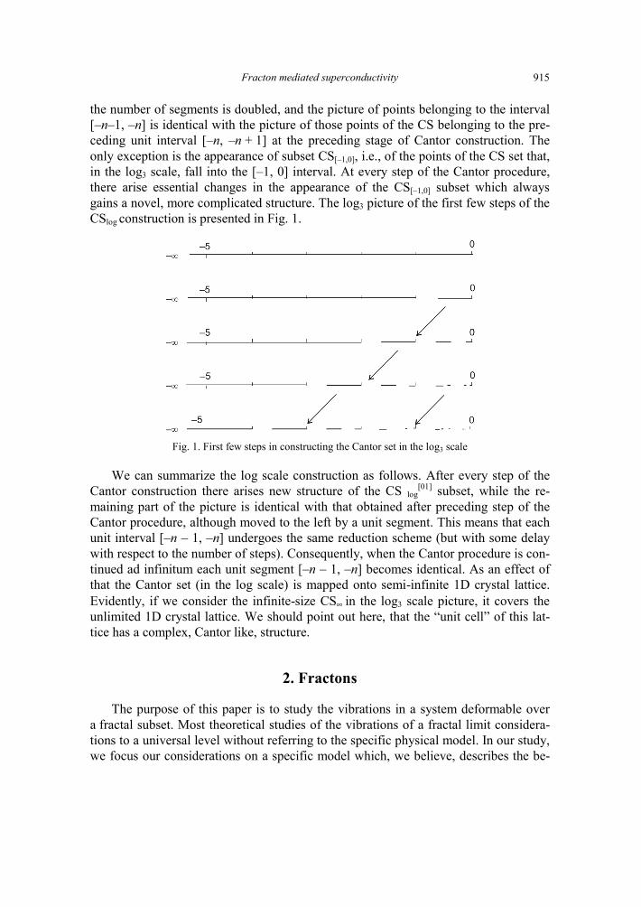
Fracton mediated superconductivity
915
the number of segments is doubled, and the picture of points belonging to the interval [–n–1, –n] is identical with the picture of those points of the CS belonging to the pre-ceding unit interval [–n, –n + 1] at the preceding stage of Cantor construction. The only exception is the appearance of subset CS[–1,0], i.e., of the points of the CS set that, in the log3 scale, fall into the [–1, 0] interval. At every step of the Cantor procedure, there arise essential changes in the appearance of the CS[–1,0] subset which always gains a novel, more complicated structure. The log3 picture of the first few steps of the CSlog construction is presented in Fig. 1.
Fig. 1. First few steps in constructing the Cantor set in the log3 scale
We can summarize the log scale construction as follows. After every step of the Cantor construction there arises new structure of the CS log
[01] subset, while the re-maining part of the picture is identical with that obtained after preceding step of the Cantor procedure, although moved to the left by a unit segment. This means that each unit interval [–n – 1, –n] undergoes the same reduction scheme (but with some delay with respect to the number of steps). Consequently, when the Cantor procedure is con-tinued ad infinitum each unit segment [–n – 1, –n] becomes identical. As an effect of that the Cantor set (in the log scale) is mapped onto semi-infinite 1D crystal lattice. Evidently, if we consider the infinite-size CS∞ in the log3 scale picture, it covers the unlimited 1D crystal lattice. We should point out here, that the “unit cell” of this lat-tice has a complex, Cantor like, structure.
2. Fractons
The purpose of this paper is to study the vibrations in a system deformable over a fractal subset. Most theoretical studies of the vibrations of a fractal limit considera-tions to a universal level without referring to the specific physical model. In our study, we focus our considerations on a specific model which, we believe, describes the be-
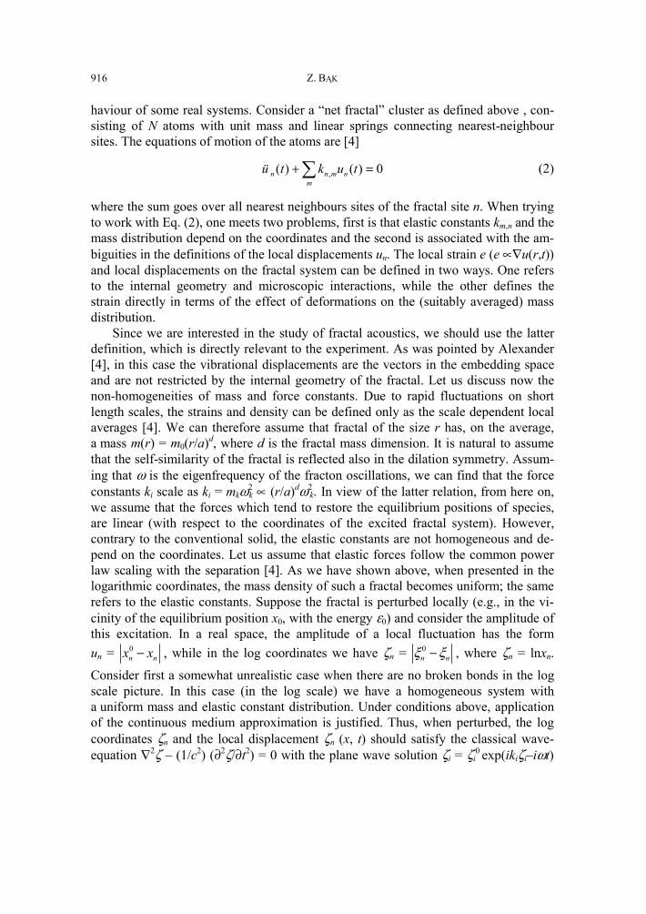
Z. BĄK
916
haviour of some real systems. Consider a “net fractal” cluster as defined above , con-sisting of N atoms with unit mass and linear springs connecting nearest-neighbour sites. The equations of motion of the atoms are [4]
,( ) ( ) 0n n m nm
ü t k u t+ =∑ (2)
where the sum goes over all nearest neighbours sites of the fractal site n. When trying to work with Eq. (2), one meets two problems, first is that elastic constants km,n and the mass distribution depend on the coordinates and the second is associated with the am-biguities in the definitions of the local displacements un. The local strain e (e ∝∇u(r,t)) and local displacements on the fractal system can be defined in two ways. One refers to the internal geometry and microscopic interactions, while the other defines the strain directly in terms of the effect of deformations on the (suitably averaged) mass distribution.
Since we are interested in the study of fractal acoustics, we should use the latter definition, which is directly relevant to the experiment. As was pointed by Alexander [4], in this case the vibrational displacements are the vectors in the embedding space and are not restricted by the internal geometry of the fractal. Let us discuss now the non-homogeneities of mass and force constants. Due to rapid fluctuations on short length scales, the strains and density can be defined only as the scale dependent local averages [4]. We can therefore assume that fractal of the size r has, on the average, a mass m(r) = m0(r/a)d, where d is the fractal mass dimension. It is natural to assume that the self-similarity of the fractal is reflected also in the dilation symmetry. Assum-ing that ω is the eigenfrequency of the fracton oscillations, we can find that the force constants ki scale as ki = mkω2
k ∝ (r/a)dω2k. In view of the latter relation, from here on,
we assume that the forces which tend to restore the equilibrium positions of species, are linear (with respect to the coordinates of the excited fractal system). However, contrary to the conventional solid, the elastic constants are not homogeneous and de-pend on the coordinates. Let us assume that elastic forces follow the common power law scaling with the separation [4]. As we have shown above, when presented in the logarithmic coordinates, the mass density of such a fractal becomes uniform; the same refers to the elastic constants. Suppose the fractal is perturbed locally (e.g., in the vi-cinity of the equilibrium position x0, with the energy ε0) and consider the amplitude of this excitation. In a real space, the amplitude of a local fluctuation has the form un = 0
n nx x− , while in the log coordinates we have ζn = 0n nξ ξ− , where ζn = lnxn.
Consider first a somewhat unrealistic case when there are no broken bonds in the log scale picture. In this case (in the log scale) we have a homogeneous system with a uniform mass and elastic constant distribution. Under conditions above, application of the continuous medium approximation is justified. Thus, when perturbed, the log coordinates ζn and the local displacement ζn (x, t) should satisfy the classical wave-equation ∇2ζ – (1/c2) (∂2ζ/∂t2) = 0 with the plane wave solution ζi = ζi
0 exp(ikiζi–iωt)
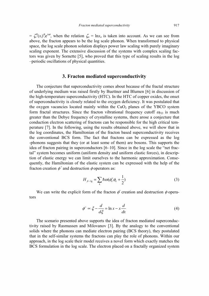
Fracton mediated superconductivity
917
= ζi0(xi)ik
ieiωt, when the relation ζn = lnxn is taken into account. As we can see from above, the fracton appears to be the log scale phonon. When transformed to physical space, the log scale phonon solution displays power law scaling with purely imaginary scaling exponent. The extensive discussion of the systems with complex scaling fac-tors was given by Sornette [5], who proved that this type of scaling results in the log –periodic oscillations of physical quantities.
3. Fracton mediated superconductivity
The conjecture that superconductivity comes about because of the fractal structure of underlying medium was raised firstly by Buettner and Blumen [6] in discussion of the high-temperature superconductivity (HTC). In the HTC of copper oxides, the onset of superconductivity is closely related to the oxygen deficiency. It was postulated that the oxygen vacancies located mainly within the CuO2 planes of the YBCO system form fractal structures. Since the fracton vibrational frequency cutoff ωFD is much greater than the Debye frequency of crystalline systems, there arose a conjecture that conduction electron scattering of fractons can be responsible for the high critical tem-perature [7]. In the following, using the results obtained above, we will show that in the log coordinates, the Hamiltonian of the fracton based superconductivity receives the conventional BCS form. The fact that fractons can be expressed as the log -phonons suggests that they (or at least some of them) are bosons. This supports the idea of fracton pairing in superconductors [6–10]. Since in the log scale the “net frac-tal” system becomes uniform (uniform density and uniform elastic forces), in descrip-tion of elastic energy we can limit ourselves to the harmonic approximation. Conse-quently, the Hamiltonian of the elastic system can be expressed with the help of the fracton creation φ + and destruction φ operators as:
lg1( )2fr k k
kH ω φ φ+− = +∑ (3)
We can write the explicit form of the fracton φ+ creation and destruction φ opera-tors
lnd dx xd dx
φ ξξ
+ ∝ − = − (4)
The scenario presented above supports the idea of fracton mediated superconduc-tivity raised by Rasmussen and Milovanov [3]. By the analogy to the conventional solids where the phonons can mediate electron pairing (BCS theory), they postulated that in the self-similar systems the fractons can play the role of phonons. Within our approach, in the log scale their model receives a novel form which exactly matches the BCS formulation in the log scale. The electron placed on a fractally organized system
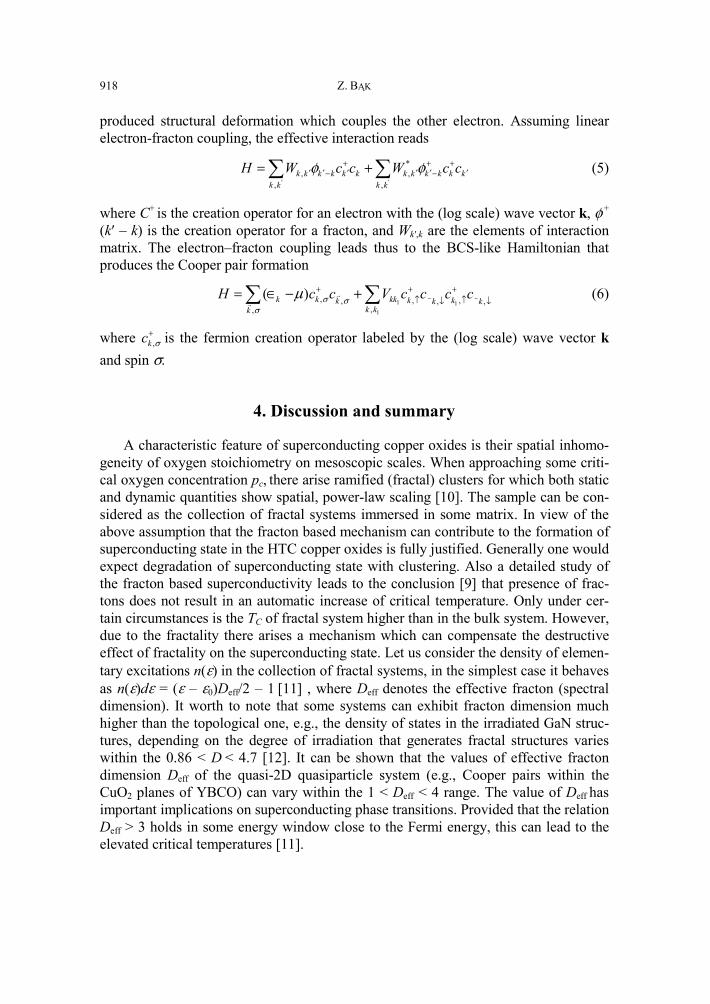
Z. BĄK
918
produced structural deformation which couples the other electron. Assuming linear electron-fracton coupling, the effective interaction reads
' '
*, ,
, ,k k k k k k k k k k k k
k k k k
H W c c W c cφ φ+ + +′ ′ ′ ′ ′ ′− −= +∑ ∑ (5)
where C+ is the creation operator for an electron with the (log scale) wave vector k, φ +
(k′ – k) is the creation operator for a fracton, and Wk′,k are the elements of interaction matrix. The electron–fracton coupling leads thus to the BCS-like Hamiltonian that produces the Cooper pair formation
1 1
1
, , ,, , ,,,
( )k k kk k kk k kk kk
H c c V c c c cσ σσ
μ − −+ + +
↑ ↑↓ ↓= ∈ − +∑ ∑ (6)
where ,kc σ+ is the fermion creation operator labeled by the (log scale) wave vector k
and spin σ.
4. Discussion and summary
A characteristic feature of superconducting copper oxides is their spatial inhomo-geneity of oxygen stoichiometry on mesoscopic scales. When approaching some criti-cal oxygen concentration pc, there arise ramified (fractal) clusters for which both static and dynamic quantities show spatial, power-law scaling [10]. The sample can be con-sidered as the collection of fractal systems immersed in some matrix. In view of the above assumption that the fracton based mechanism can contribute to the formation of superconducting state in the HTC copper oxides is fully justified. Generally one would expect degradation of superconducting state with clustering. Also a detailed study of the fracton based superconductivity leads to the conclusion [9] that presence of frac-tons does not result in an automatic increase of critical temperature. Only under cer-tain circumstances is the TC of fractal system higher than in the bulk system. However, due to the fractality there arises a mechanism which can compensate the destructive effect of fractality on the superconducting state. Let us consider the density of elemen-tary excitations n(ε) in the collection of fractal systems, in the simplest case it behaves as n(ε)dε = (ε – ε0)Deff/2 – 1 [11] , where Deff denotes the effective fracton (spectral dimension). It worth to note that some systems can exhibit fracton dimension much higher than the topological one, e.g., the density of states in the irradiated GaN struc-tures, depending on the degree of irradiation that generates fractal structures varies within the 0.86 < D < 4.7 [12]. It can be shown that the values of effective fracton dimension Deff of the quasi-2D quasiparticle system (e.g., Cooper pairs within the CuO2 planes of YBCO) can vary within the 1 < Deff < 4 range. The value of Deff has important implications on superconducting phase transitions. Provided that the relation Deff > 3 holds in some energy window close to the Fermi energy, this can lead to the elevated critical temperatures [11].
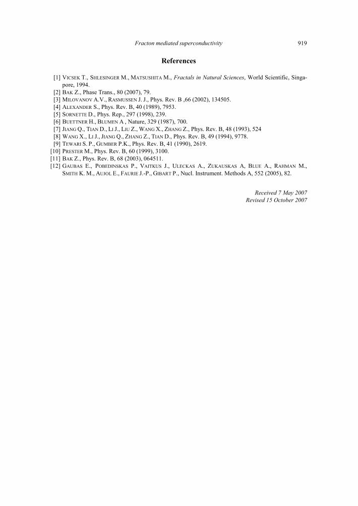
Fracton mediated superconductivity
919
References
[1] VICSEK T., SHLESINGER M., MATSUSHITA M., Fractals in Natural Sciences, World Scientific, Singa-pore, 1994.
[2] BAK Z., Phase Trans., 80 (2007), 79. [3] MILOVANOV A.V., RASMUSSEN J. J., Phys. Rev. B ,66 (2002), 134505. [4] ALEXANDER S., Phys. Rev. B, 40 (1989), 7953. [5] SORNETTE D., Phys. Rep., 297 (1998), 239. [6] BUETTNER H., BLUMEN A , Nature, 329 (1987), 700. [7] JIANG Q., TIAN D., LI J., LIU Z., WANG X., ZHANG Z., Phys. Rev. B, 48 (1993), 524 [8] WANG X., LI J., JIANG Q., ZHANG Z., TIAN D., Phys. Rev. B, 49 (1994), 9778. [9] TEWARI S. P., GUMBER P.K., Phys. Rev. B, 41 (1990), 2619.
[10] PRESTER M., Phys. Rev. B, 60 (1999), 3100. [11] BAK Z., Phys. Rev. B, 68 (2003), 064511. [12] GAUBAS E., POBEDINSKAS P., VAITKUS J., ULECKAS A., ZUKAUSKAS A, BLUE A., RAHMAN M.,
SMITH K. M., AUJOL E., FAURIE J.-P., GIBART P., Nucl. Instrument. Methods A, 552 (2005), 82.
Received 7 May 2007 Revised 15 October 2007
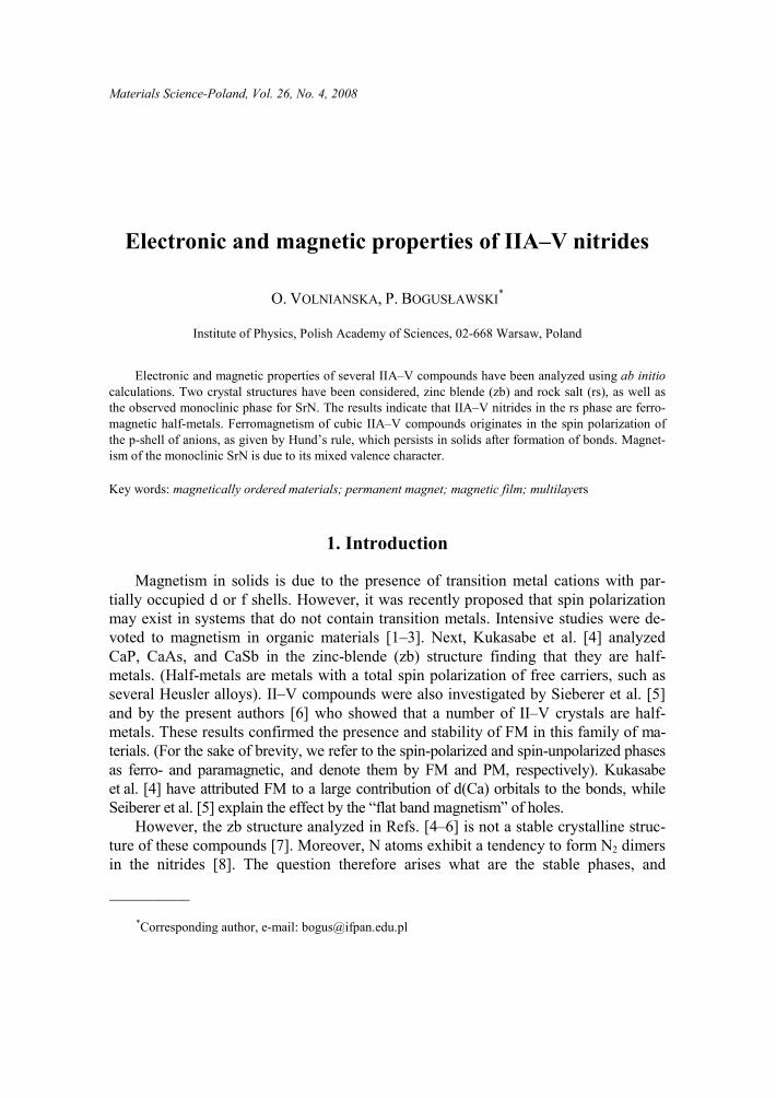
Materials Science-Poland, Vol. 26, No. 4, 2008
Electronic and magnetic properties of IIA–V nitrides
O. VOLNIANSKA, P. BOGUSŁAWSKI*
Institute of Physics, Polish Academy of Sciences, 02-668 Warsaw, Poland
Electronic and magnetic properties of several IIA–V compounds have been analyzed using ab initio calculations. Two crystal structures have been considered, zinc blende (zb) and rock salt (rs), as well as the observed monoclinic phase for SrN. The results indicate that IIA–V nitrides in the rs phase are ferro-magnetic half-metals. Ferromagnetism of cubic IIA–V compounds originates in the spin polarization of the p-shell of anions, as given by Hund’s rule, which persists in solids after formation of bonds. Magnet-ism of the monoclinic SrN is due to its mixed valence character.
Key words: magnetically ordered materials; permanent magnet; magnetic film; multilayers
1. Introduction
Magnetism in solids is due to the presence of transition metal cations with par-tially occupied d or f shells. However, it was recently proposed that spin polarization may exist in systems that do not contain transition metals. Intensive studies were de-voted to magnetism in organic materials [1–3]. Next, Kukasabe et al. [4] analyzed CaP, CaAs, and CaSb in the zinc-blende (zb) structure finding that they are half-metals. (Half-metals are metals with a total spin polarization of free carriers, such as several Heusler alloys). II–V compounds were also investigated by Sieberer et al. [5] and by the present authors [6] who showed that a number of II–V crystals are half-metals. These results confirmed the presence and stability of FM in this family of ma-terials. (For the sake of brevity, we refer to the spin-polarized and spin-unpolarized phases as ferro- and paramagnetic, and denote them by FM and PM, respectively). Kukasabe et al. [4] have attributed FM to a large contribution of d(Ca) orbitals to the bonds, while Seiberer et al. [5] explain the effect by the “flat band magnetism” of holes.
However, the zb structure analyzed in Refs. [4–6] is not a stable crystalline struc-ture of these compounds [7]. Moreover, N atoms exhibit a tendency to form N2 dimers in the nitrides [8]. The question therefore arises what are the stable phases, and
__________
*Corresponding author, e-mail: [email protected]
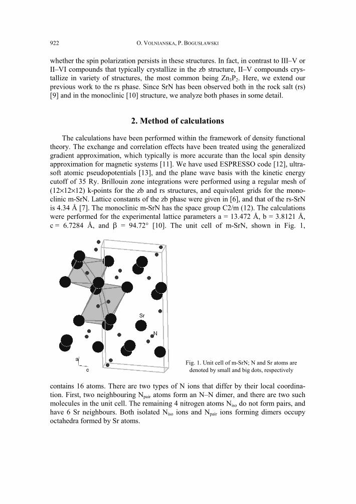
O. VOL922
whether the spin polarization persisII–VI compounds that typically crytallize in variety of structures, the previous work to the rs phase. Sinc[9] and in the monoclinic [10] struc
2. Met
The calculations have been pertheory. The exchange and correlatigradient approximation, which typapproximation for magnetic systemsoft atomic pseudopotentials [13], cutoff of 35 Ry. Brillouin zone int(12×12×12) k-points for the zb andclinic m-SrN. Lattice constants of this 4.34 Å [7]. The monoclinic m-Srwere performed for the experimentc = 6.7284 Å, and β = 94.72° [
contains 16 atoms. There are two ttion. First, two neighbouring Npair amolecules in the unit cell. The remhave 6 Sr neighbours. Both isolateoctahedra formed by Sr atoms.
LNIANSKA, P. BOGUSŁAWSKI
sts in these structures. In fact, in contrast to III–V oystallize in the zb structure, II–V compounds crys
most common being Zn3P2. Here, we extend ouce SrN has been observed both in the rock salt (rscture, we analyze both phases in some detail.
thod of calculations
rformed within the framework of density functionaion effects have been treated using the generalizeically is more accurate than the local spin densit
ms [11]. We have used ESPRESSO code [12], ultraand the plane wave basis with the kinetic energy
tegrations were performed using a regular mesh od rs structures, and equivalent grids for the monohe zb phase were given in [6], and that of the rs-SrNrN has the space group C2/m (12). The calculationtal lattice parameters a = 13.472 Å, b = 3.8121 Å[10]. The unit cell of m-SrN, shown in Fig. 1
Fig. 1. Unit cell of m-SrN; N and Sr atoms are
denoted by small and big dots, respectively
types of N ions that differ by their local coordinaatoms form an N–N dimer, and there are two suchaining 4 nitrogen atoms Niso do not form pairs, aned Niso ions and Npair ions forming dimers occupy
or s-ur s)
al d y
a-y
of o-N ns Å, 1,
a-h d y
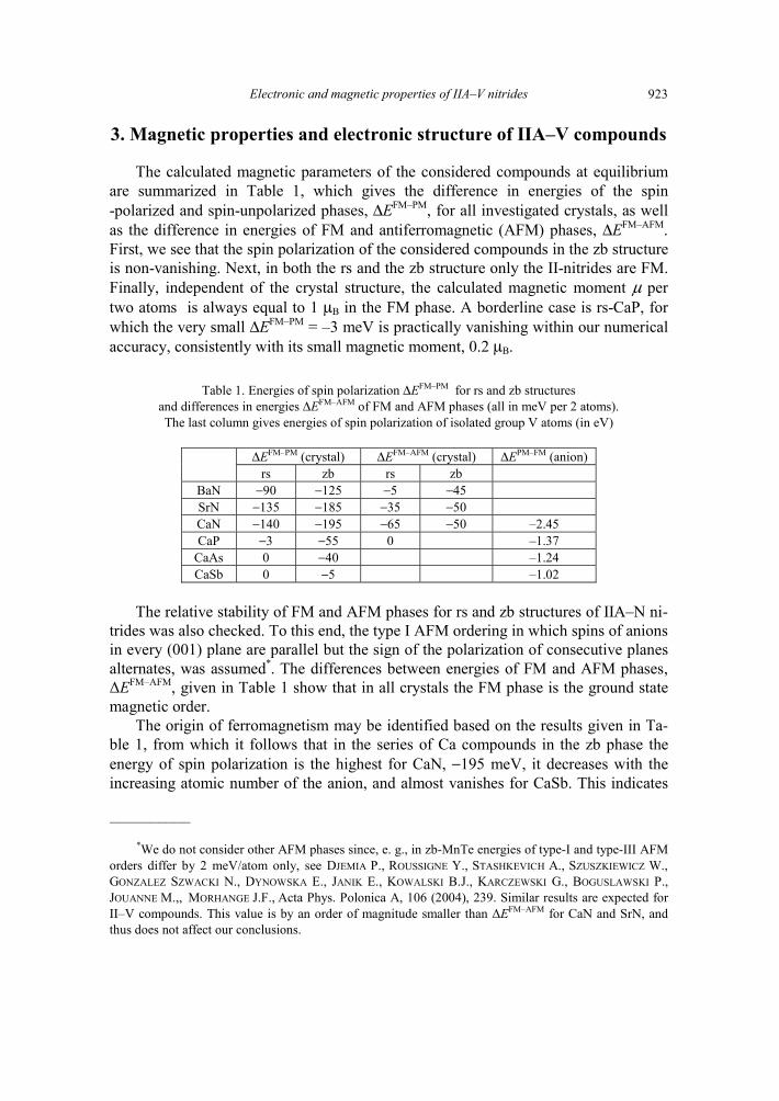
Electronic and magnetic properties of IIA–V nitrides 923
3. Magnetic properties and electronic structure of IIA–V compounds
The calculated magnetic parameters of the considered compounds at equilibrium are summarized in Table 1, which gives the difference in energies of the spin -polarized and spin-unpolarized phases, ΔEFM–PM, for all investigated crystals, as well as the difference in energies of FM and antiferromagnetic (AFM) phases, ΔEFM–AFM. First, we see that the spin polarization of the considered compounds in the zb structure is non-vanishing. Next, in both the rs and the zb structure only the II-nitrides are FM. Finally, independent of the crystal structure, the calculated magnetic moment μ per two atoms is always equal to 1 μB in the FM phase. A borderline case is rs-CaP, for which the very small ΔEFM–PM = –3 meV is practically vanishing within our numerical accuracy, consistently with its small magnetic moment, 0.2 μB.
Table 1. Energies of spin polarization ΔEFM–PM for rs and zb structures and differences in energies ΔEFM–AFM of FM and AFM phases (all in meV per 2 atoms). The last column gives energies of spin polarization of isolated group V atoms (in eV)
ΔEFM–PM (crystal) ΔEFM–AFM (crystal) ΔEPM–FM (anion) rs zb rs zb
BaN −90 −125 −5 −45 SrN −135 −185 −35 −50 CaN −140 −195 −65 −50 –2.45 CaP −3 −55 0 –1.37
CaAs 0 −40 –1.24 CaSb 0 −5 –1.02
The relative stability of FM and AFM phases for rs and zb structures of IIA–N ni-
trides was also checked. To this end, the type I AFM ordering in which spins of anions in every (001) plane are parallel but the sign of the polarization of consecutive planes alternates, was assumed*. The differences between energies of FM and AFM phases, ΔEFM–AFM, given in Table 1 show that in all crystals the FM phase is the ground state magnetic order.
The origin of ferromagnetism may be identified based on the results given in Ta-ble 1, from which it follows that in the series of Ca compounds in the zb phase the energy of spin polarization is the highest for CaN, −195 meV, it decreases with the increasing atomic number of the anion, and almost vanishes for CaSb. This indicates
__________
*We do not consider other AFM phases since, e. g., in zb-MnTe energies of type-I and type-III AFM orders differ by 2 meV/atom only, see DJEMIA P., ROUSSIGNE Y., STASHKEVICH A., SZUSZKIEWICZ W., GONZALEZ SZWACKI N., DYNOWSKA E., JANIK E., KOWALSKI B.J., KARCZEWSKI G., BOGUSLAWSKI P., JOUANNE M.,, MORHANGE J.F., Acta Phys. Polonica A, 106 (2004), 239. Similar results are expected for II–V compounds. This value is by an order of magnitude smaller than ΔEFM–AFM for CaN and SrN, and thus does not affect our conclusions.
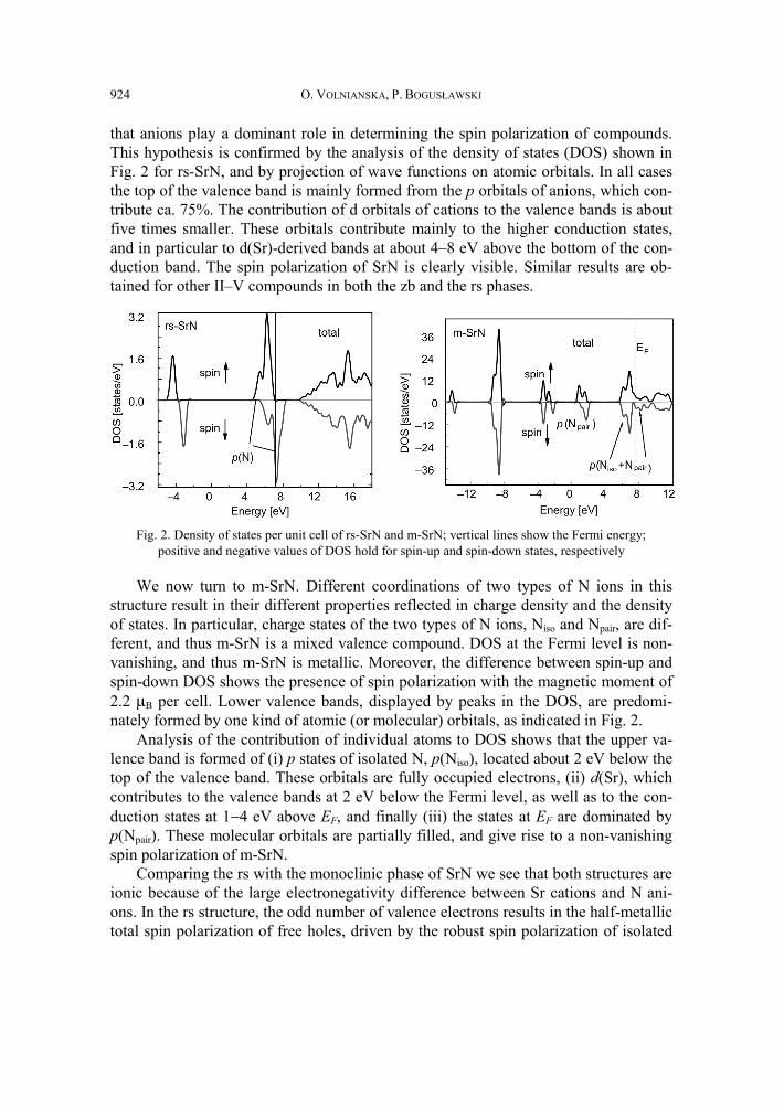
O. VOLNIANSKA, P. BOGUSŁAWSKI 924
that anions play a dominant role in determining the spin polarization of compounds. This hypothesis is confirmed by the analysis of the density of states (DOS) shown in Fig. 2 for rs-SrN, and by projection of wave functions on atomic orbitals. In all cases the top of the valence band is mainly formed from the p orbitals of anions, which con-tribute ca. 75%. The contribution of d orbitals of cations to the valence bands is about five times smaller. These orbitals contribute mainly to the higher conduction states, and in particular to d(Sr)-derived bands at about 4–8 eV above the bottom of the con-duction band. The spin polarization of SrN is clearly visible. Similar results are ob-tained for other II–V compounds in both the zb and the rs phases.
Fig. 2. Density of states per unit cell of rs-SrN and m-SrN; vertical lines show the Fermi energy; positive and negative values of DOS hold for spin-up and spin-down states, respectively
We now turn to m-SrN. Different coordinations of two types of N ions in this structure result in their different properties reflected in charge density and the density of states. In particular, charge states of the two types of N ions, Niso and Npair, are dif-ferent, and thus m-SrN is a mixed valence compound. DOS at the Fermi level is non-vanishing, and thus m-SrN is metallic. Moreover, the difference between spin-up and spin-down DOS shows the presence of spin polarization with the magnetic moment of 2.2 μB per cell. Lower valence bands, displayed by peaks in the DOS, are predomi-nately formed by one kind of atomic (or molecular) orbitals, as indicated in Fig. 2.
Analysis of the contribution of individual atoms to DOS shows that the upper va-lence band is formed of (i) p states of isolated N, p(Niso), located about 2 eV below the top of the valence band. These orbitals are fully occupied electrons, (ii) d(Sr), which contributes to the valence bands at 2 eV below the Fermi level, as well as to the con-duction states at 1−4 eV above EF, and finally (iii) the states at EF are dominated by p(Npair). These molecular orbitals are partially filled, and give rise to a non-vanishing spin polarization of m-SrN.
Comparing the rs with the monoclinic phase of SrN we see that both structures are ionic because of the large electronegativity difference between Sr cations and N ani-ons. In the rs structure, the odd number of valence electrons results in the half-metallic total spin polarization of free holes, driven by the robust spin polarization of isolated
Electronic and magnetic properties of IIA–V nitrides 925
N atoms. In m-SrN, there are two kinds of N ions which are in different charge states, which imply that they are in a different spin state as well. For this reason, in the nota-tion used by chemists [10], in the monoclinic phase SrN is denoted by Sr4[2N3−][N2
2−], pointing out the fact that Niso in the 3– state are non-magnetic and closed-shell ions, while Npair are partially spin polarized. The most important result is that SrN in both structures is magnetic in spite of the absence of transition metal atoms.
4. Summary
Using ab initio calculations we have studied magnetic and electronic structure of a number of IIA–V compounds in the zb and rs structures. The calculated spin polari-zation owns its origin to the spin polarization of group V anions. The atomic spin po-larization is the strongest for nitrogen, which explains stability of magnetization in CaN, SrN, and BaN nitrides, and the lack of magnetization in rs phosphides and ar-senides. SrN was found to be magnetic in both rs and monoclinic structures. In the latter case, magnetism stems from the mixed valence character of m-SrN.
Acknowledgements
The authors thank Paweł Jakubas for his valuable help in numerical calculations. The calculations were performed at Interdisciplinary Centre for Mathematical and Computational Modeling, Warsaw University.
References
[1] MAKAROVA T.L., SUNDQUIST B., HOHNE R., ESQUINAZI P., KOPELEVICH Y., SCHARFF P., DAVIDOV V.A., KASHEVAROVA L.S., RAKHMANINA A.V., Nature, 413 (2001), 716.
[2] WOOD R.A., LEWIS M.H., LEES M.R., BENNINGTON S.M., CAIN M.G., KITAMURA N., J. Phys.: Con-dens. Matter, 14 (2002), L385.
[3] ESQUINAZI P., SPEMANN D., HOHNE R., SETZER A., HAN K.-H., BUTZ T., Phys. Rev. Lett., 91 (2003), 227201.
[4] KUKASABE K., GESHI M., TSUKAMOTO H., SUZUKI N., J. Phys. C: Condens. Matter, 16 (2004), 5639. [5] SIEBERER M., REDINGER J., KHMELEVSKYI S., MOHN P., Phys. Rev. B, 73 (2006), 024404. [6] VOLNIANSKA O., JAKUBAS P., BOGUSLAWSKI P., J. Alloys Compd., 423 (2006), 191. [7] VOLNIANSKA O., BOGUSLAWSKI P., Phys. Rev. B, 75 (2007), 224418. [8] GROCHALA W., Collect. Czech. Chem. Commun., 71 (2006), 1525. [9] GAUDE J., L’HARIDON P., LAURENT Y., LANG J., Rev. Chim. Minerale, 8 (1971), 287.
[10] AUFFERMANN G., PROTS YU., KNIEP R., Angew. Chem. Int. Ed., 40 (2001), 547. [11] PERDEW J.P., BURKE K., ERNZERHOF M., Phys. Rev. Lett., 77 (1996), 3865. [12] http://www.pwscf.org. [13] VANDERBILT D., Phys. Rev. B 41 (1990), 7892(R).
Received 7 May 2007 Revised 15 October 2007
Materials Science-Poland, Vol. 26, No. 4, 2008
Transport and magnetic properties of Ge1–x–y Mnx(Eu,Yb)yTe semimagnetic semiconductors
B. BRODOWSKA1*, I. KURYLISZYN-KUDELSKA1, M. ARCISZEWSKA1, K. DYBKO1, V. DOMUKHOVSKI1, W. DOBROWOLSKI1, V.E. SLYNKO2, E.I. SLYNKO2, V.K. DUGAEV3
1Institute of Physics, Polish Academy of Sciences, al. Lotników 32/46, 02-668 Warsaw, Poland 2Institute for Problems of Material Science, NASU, Vilde 5, 58001 Chernovtsy, Ukraine 3Department of Mathematics and Applied Physics, Rzeszów University of Technology,
al. Powstańców Warszawy 6, 35-959 Rzeszów, Poland
Transport and magnetic properties of the IV−VI ferromagnetic multinary mixed compounds Ge1–xMnxTe, Ge1–x–yMnxEuyTe and Ge1–x–yMnxYbyTe (0.045 ≤ x ≤ 0.47, y < 0.04) were investigated in magnetic fields up to 13 T and in the temperature range 1.6–300 K. The Curie temperatures of studied samples exceed 100 K. Based on the dependences of the Hall resistivity and magnetization on magnetic field, the anomalous Hall coefficients RS were calculated, and RS dependences on crystal composition and temperature were found.
Key words: semimagnetic semiconductor; diluted magnetic semiconductor; anomalous Hall effect
1. Introduction
It has been well known from early 70s that even a small admixture of MnTe in GeTe leads to the ferromagnetic behaviour of the resulting alloy [1]. The mixed com-pound Ge1–xMnxTe for x < 0.18 crystallizes in the rhombohedrally distorted NaCl structure. Ge1–xMnxTe belongs to the interesting class of materials which simulta-neously reveal ferromagnetic and ferroelectric properties [2]. These features may lead to interesting applications in spintronic devices. Ge1–xMnxTe crystals are always p-type and the ferromagnetism is accounted to the Ruderman–Kittel–Kasuya–Yosida interac-tion [3] which proceeds via a coupling between the ion and the mobile charge carriers. The magnetic Curie temperature depends on both the Mn content and the carrier con-centration, and its highest reported value does not exceed 160 K. In our recent paper, we revealed that a small admixture of rare earth ion Eu in GeMnTe substantially in-creased the ferromagnet–paramagnet phase transition temperature [4]. The effect is not __________
*Corresponding author, e-mail: [email protected]
B. BRODOWSKA et al. 928
yet fully understood, and some attempts of possible explanations may be found in [4]. In the present paper, we report results of magnetotransport and magnetic studies of the bulk crystals of Ge1–xMnxTe as well as Ge1–xMnxTe codoped with Eu and Yb. Based on the dependences of Hall resistivity and magnetization on magnetic field, the ano-malous Hall coefficient RS was calculated, and RS dependences on crystal composition and temperature were determined.
2. Experimental
The Ge1–xMnxTe, Ge1–x–yMnxEuyTe and Ge1–x–yMnxYbyTe bulk crystals used in this study were grown by the modified Bridgman method. The chemical compositions of the crystals were determined by the X-ray dispersive fluorescence technique. The manganese content x was found to be in the range 4.5–47 at. % while the rare earth ions content did not exceed 4 at. %. The X-ray powder diffraction studies showed that the crystals were single-phase, except the samples Ge1–x–y MnxTe – 960_12 and Ge1–x–yMnxYbyTe − 971_12, where the traces of a second phase were visible. The sample compositions and carrier concentrations derived from the transport measurements are given in Table 1.
Table 1. Samples characteristics
Sample symbol Composition [molar fraction]
Hole concentration[cm–3]
Ge1–xMnxTe − 960_2 x = 0.045 1.04×10²¹ Ge1–xMnxTe − 960_12 x = 0.388 2.86×10²¹ Ge1–x–yMnxEuyTe − 849_8 x = 0.087, y = 0.038 1.06×10²¹ Ge1–x–yMnxEuyTe − 849_16 x = 0.073, y = 0.03 1.01×10²¹ Ge1–x–yMnxYbyTe − 971_12 x = 0.47, y = 0.004 4.16×10²¹
The magnetic properties were studied by use of the Lake Shore 7229 DC magne-
tometer/AC susceptometer system: ac magnetic susceptibility in function of tempera-ture up to 170 K (by means of a standard mutual inductance method), and magnetiza-tion in magnetic fields B up to 9 T (by an extraction method) in the temperature range 1.5–170 K. The examples of dependences of the ac susceptibility on temperature are presented in Fig. 1. The magnetization curves vs. magnetic field for two samples are shown in Fig. 2. It may be noted that in the available range of magnetic fields we do not observe the saturation of magnetization, particularly large discrepancies between experimental values and the expected ones were observed for the samples with the highest manganese contents. For example, the theoretically calculated saturation mag-netization for the sample Ge1–x–yMnxYbyTe 971_12 (see Fig. 2) equals 68.3 emu/g, approximately three times higher than the experimental value obtained at 9 T. This phenomenon is likely due to the presence of antiferromagnetic nanoinclusions assem-bled due to chemical or crystallographic phase separations. These nanoclusters are below the detection limit of the conventional powder diffraction method. Nanoinclu-sions (of ferromagnetic or antiferromagnetic nature) were found in several semimag-
Transport and magnetic properties of Ge1–x–y Mnx(Eu,Yb)yTe semimagnetic semiconductors 929
netic materials [5], and it was established that their presence significantly modifies properties of the host material.
Fig. 1. Magnetic susceptibility of: a) – Ge1–xMnxTe, x = 0.388, – Ge1–x–yMnxYbyTe,
x = 0.47, y = 0.004, b) – Ge1–xMnxTe, x = 0.045, – Ge1–x–yMnxEuyTe, x = 0.087, y = 0.038
Fig. 2. Magnetization of selected samples for low (a) and high (b) manganese contents,
at three temperatures below and near (above) the Curie temperature
The Hall resistivity and electric conductivity measurements were carried out using a standard dc technique in the continuous-flow helium cryostat in the temperature range 1.5–170 K in magnetic fields up to 13 T. A typical six-contact sample configu-ration, which allows both the sample resistance and Hall voltage to be measured si-
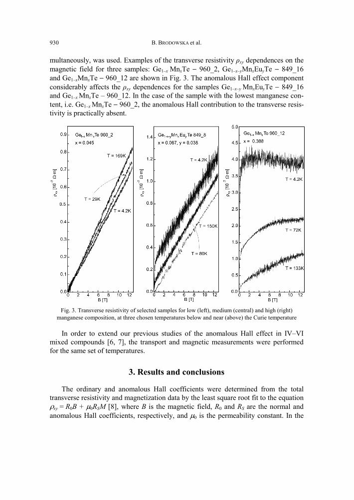
B. BRODOWSKA et al. 930
multaneously, was used. Examples of the transverse resistivity ρxy dependences on the magnetic field for three samples: Ge1–x MnxTe − 960_2, Ge1–x–yMnxEuyTe − 849_16 and Ge1–xMnxTe − 960_12 are shown in Fig. 3. The anomalous Hall effect component considerably affects the ρxy dependences for the samples Ge1–x–y MnxEuyTe − 849_16 and Ge1–x MnxTe – 960_12. In the case of the sample with the lowest manganese con-tent, i.e. Ge1–x MnxTe − 960_2, the anomalous Hall contribution to the transverse resis-tivity is practically absent.
Fig. 3. Transverse resistivity of selected samples for low (left), medium (central) and high (right) manganese composition, at three chosen temperatures below and near (above) the Curie temperature
In order to extend our previous studies of the anomalous Hall effect in IV–VI mixed compounds [6, 7], the transport and magnetic measurements were performed for the same set of temperatures.
3. Results and conclusions
The ordinary and anomalous Hall coefficients were determined from the total transverse resistivity and magnetization data by the least square root fit to the equation ρxy = R0B + μ0RSM [8], where B is the magnetic field, R0 and RS are the normal and anomalous Hall coefficients, respectively, and μ0 is the permeability constant. In the
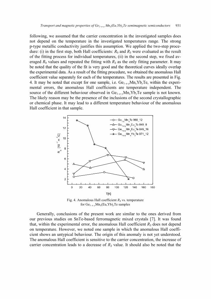
Transport and magnetic properties of Ge1–x–y Mnx(Eu,Yb)yTe semimagnetic semiconductors 931
following, we assumed that the carrier concentration in the investigated samples does not depend on the temperature in the investigated temperatures range. The strong p-type metallic conductivity justifies this assumption. We applied the two-step proce-dure: (i) in the first step, both Hall coefficients: R0 and RS were evaluated as the result of the fitting process for individual temperatures, (ii) in the second step, we fixed av-eraged R0 values and repeated the fitting with RS as the only fitting parameter. It may be noted that the quality of the fit is very good and the theoretical curves ideally overlap the experimental data. As a result of the fitting procedure, we obtained the anomalous Hall coefficient value separately for each of the temperatures. The results are presented in Fig. 4. It may be noted that except for one sample, i.e. Ge1–x–yMnxYbyTe, within the experi-mental errors, the anomalous Hall coefficients are temperature independent. The source of the different behaviour observed in Ge1–x–yMnxYbyTe sample is not known. The likely reason may be the presence of the inclusions of the second crystallographic or chemical phase. It may lead to a different temperature behaviour of the anomalous Hall coefficient in that sample.
Fig. 4. Anomalous Hall coefficient RS vs. temperature
for Ge1–x–yMnx(Eu,Yb)yTe samples
Generally, conclusions of the present work are similar to the ones derived from our previous studies on SnTe-based ferromagnetic mixed crystals [7]. It was found that, within the experimental error, the anomalous Hall coefficient RS does not depend on temperature. However, we noted one sample in which the anomalous Hall coeffi-cient shows an untypical behaviour. The origin of this anomaly is not yet understood. The anomalous Hall coefficient is sensitive to the carrier concentration, the increase of carrier concentration leads to a decrease of RS value. It should also be noted that the
B. BRODOWSKA et al. 932
absolute values of the anomalous Hall coefficient are of the same order in the both investigated systems, SnTe-based as well as GeTe-based.
References
[1] RODOT M., LEWIS J., RODOT H., VILLERS G., COHEN J., MOLLARD P., J. Phys. Soc. Japan, Suppl., 21 (1966), 627.
[2] GAŁĄZKA R.R., KOSSUT J., STORY T., Semimagnetic semiconductors, [in:] Numerical Data and Func-tional Relationships in Science and Technology Group III: Condensed Matter, W. Martienssen (Ed.), Vol. 41, Suppl. to Vols. III/17b, 22a, Springer, Berlin, 1999, p. 647.
[3] COCHRANE R.W., HEDGCOCK F.T., STRÖM-OLSEN J.O., Phys. Rev. B, 8 (1973), 4262. [4] DOBROWOLSKI W., ARCISZEWSKA M., BRODOWSKA B., DOMUKHOVSKI V., DUGAEV V.K., GRZEDA A.,
KURYLISZYN-KUDELSKA I., WOJCIK M., SLYNKO E.I., Sci. Sint., 38 (2006), 109. [5] DIETL T., Acta Phys. Polon. A, 111 (2007), 27. [6] RACKA K., KURYLISZYN I., ARCISZEWSKA M., DOBROWOLSKI W., BROTO J.-M., PORTUGALL O.,
RAKOTO H., RAQUET B., DUGAEV V., SLYNKO E.I., SLYNKO V.E., J. Supercond., 16 (2003), 289. [7] BRODOWSKA B., DOBROWOLSKI W., ARCISZEWSKA M., SLYNKO E.I., DUGAEV V.K., J. Alloys Comp.,
423 (2006), 205. [8] The Hall Effect and Its Applications, L. Chien, C.R. Westgate (Eds.), Plenum, New York, 1980.
Received 7 May 2007 Revised 23 September 2007
Materials Science-Poland, Vol. 26, No. 4, 2008
Crystallization of (Th1–xUx)3As4 ferromagnetic semiconductor from the Ga flux
P. WIŚNIEWSKI, Z. HENKIE*, A. PIETRASZKO
Institute of Low Temperature and Structure Research, Polish Academy of Sciences, P. O. Box 1410, 50-950 Wrocław 2, Poland
Crystals of n- or p-type heavily doped ferromagnetic semiconductor (Th1–xUx)3As4 (x = 0.67 and 0.80) were grown using a mineralization process in the Ga flux. An excess of As corresponding to MeAs2 composition was necessary to grow the Me3As4 phase at temperature cycled between 1000 ºC and 1060 ºC. Dilution of U3As4 ferromagnet (Curie temperature TC = 198 K) with 20% of Th3As4 semiconductor (energy gap of 0.39 eV) reduced TC by 19%.
Key words: ferromagnetic semiconductor; crystallization; actinide compounds
1. Introduction
The discovery of ferromagnetism in zinc blende III–V and II–VI Mn-based com-pounds (see [1] and references therein) allows one to explore the physics of previously unavailable combinations of quantum structure and magnetism in semiconductors. Studies of magnetic and semiconducting properties in solid state systems served as an important test for understanding basic physics and discovering new applications in spintronics [2, 3]. During last decades, the anomalous Hall resistivity and anisotropic magnetoresistance in sd electron systems were experimentally investigated to great extent, motivated by the technological importance of both effects. On the other hand, these effects originate from anisotropy of the density of states and spin-orbit interac-tion [4] which can be fairly high in f electron systems, as it is in U3As4 ferromagnet [5] and therefore we have proposed research on spintronic properties of its semiconduct-ing thorium derivatives [6].
Both U3As4 and Th3As4 crystallize in Th3P4 type structure, which belongs to the space group 43 .I d U3As4 is a low-carrier ferromagnet (Curie temperature TC = 198 K)
__________
* Corresponding autor, e-mail: [email protected]
P. WIŚNIEWSKI et al. 934
showing giant anomalous Hall resistivity and high anisotropic magnetoresistance [6, 7]. Th3As4 is an indirect gap semiconductor with energy gap of 0.39 eV [8]. Crys-tals of U3As4 could be grown by the conventional vapour transport method in a quartz ampoule [9]. This method could not be used for growing Th3As4 crystals because of a strong reaction with the quartz ampoule. Therefore a modified van Arkel method [10] has been developed. This method allowed growing either n- [11] or p-type [12] Th3As4 crystals, presumably due to their specific off-stoichiometry. These possibilities indicated (Th1–xUx)3As4 system to be more attractive for spintronic studies. Hitherto Th-rich n-type (Th1–xUx)3As4 solid solutions (up to x = 0.15) grown by the modified van Arkel method [10] remained non-ferromagnetic semiconductors down to 4 K. However, the modified van Arkel method is complicated and requires high amounts of Th and U for effective preparation of samples of examined system. Expecting coexis-tence of semiconducting and ferromagnetic properties, promising interesting spintron-ics-oriented features in U-reach (Th1–xUx)3As4 solutions [6], we look for easier and cheaper methods of preparation of such solid solutions. In this work, a possibility of growing such solid solutions using the Ga flux method has been examined.
2. Experimental
Thorium, uranium, arsenic and gallium elements in proper atomic ratios were placed in covered alumina crucibles and closed in quartz ampoules, under 150 mm Hg of argon. Then they were heated and cooled in three different ways. In experiments I, II and III the Th:U:As:Ga elements were taken with atomic ratios 1:2:4:50, 1:2:6:50 and 1:2:6:50, respectively. In the case of experiments I and II, the ampoules were heated up to 1080 ºC, annealed for 10 h, cooled down to 860 ºC at the rate 1 ºC/h, next to 500 ºC at the rate 2 ºC/h and then quickly placed in ambient temperature. In the experiment III, the ampoule was heated up to 1080 ºC, annealed for 10 h and then for two weeks repeatedly cooled down to 1000 ºC at the rate of 5 ºC/h and heated to 1060 ºC at the rate of 20 ºC/h, and then quickly placed in ambient temperature, di-rectly from the furnace (1000 ºC). Liquid gallium was removed with a syringe, its remains washed out with mercury and diluted HCl. Remains of mercury were distilled out in vacuum. The obtained material was cooled down with liquid nitrogen and the ferromagnetic phase was extracted with a strong permanent magnet.
The samples were examined with electron microscope with EDAX analysis. Crys-tal structure of selected single crystals was analysed with 4-circle X-ray diffractometer and resolved using the SHELX-97 program with a final discrepancy factors, R1, given in Table 1 [13, 14]. The dc magnetic susceptibility, χdc, in fields of 2000 Gs was measured between 1.7 and 200 K using a SQUID magnetometer. The resistivity in longitudinal fields of 0 and 1 T was measured between 60 and 200 K by conventional 4-point ac technique in an electromagnet. Thermoelectric power was estimated with a home-made thermoelectric probe.
Crystallization of (Th1–xUx)3As4 ferromagnetic semiconductor 935
Table 1. Some physical data for (Th1–xUx)3As4 compounds
Sample Composition Lattice parameter [Å]
Discrepancy factor R1
Thermoelectric power [μV/K]
II-a, -ba (Th0.2U0.8)3As4 8.587 0.035 –20 II-bc (Th0.33U0.67)3As4 8.577 0.086 +35 III (Th0.33U0.67)3As4 8.573 0.055 –5
3. Results
Experiment I resulted in a small amount of ferromagnetic phase in the form of fine powder that was not examined here. Two characteristic forms of (Th1–xUx)3As4 phase were obtained in the experiment II, labelled here as samples II-a and II-b. The sample II-a consisted of small (≈0.05 mm in diameter) ferromagnetic (Th0.2U0.8)3As4 isometric single crystals with rounded edges, partially immersed in a surface of large (ca. 2 mm) GaAs crystal (Fig. 1a). Temperature dependence of magnetization of the composite, shown in Fig. 2, yielded TC = 160 K. The second form looked like pieces of broken crust of sphere, whose concave surface (sample II-bc) was formed of bigger (Th0.33U0.67)3As4 crystals with sharp edges and thermoelectric power S ≈ 35 μV/K. A cross-section of the crust is shown in Fig. 1b where one can see the structure of the convex surface of the crust formed of small crystals of Th3P4 type crystal structure, identical with that of the first form (II-a), and thermoelectric power S ≈ –20 μV/K. After polishing out the bigger crystals from the convex surface, we obtained a sample (II-ba) of uniform S, for which temperature dependence of electrical resistance is shown in Fig. 3. It allowed us to determine TC = 150 K.
Fig. 1. SEM images: a) sample II-a immersed in GaAs surface, b) cross section of the crust surrounding U and Th and facing them with (bigger) crystals – sample II-bc and tiny crystals on the opposite side – sample II-ba, c) single (sample III) and polycrystalline (Th0.33U0.67)3As4; all bars represent 0.1 mm
The experiment III gave (Th0.33U0.67)3As4 isometric crystals, like those in sample II-a, but about twice as big and with sharper edges, as shown in Fig. 1c. The product
P. WIŚNIEWSKI et al. 936
of that experiment contained also small thin plates of GaAs. Some physical quantities describing the examined samples are collected in Table 1.
Fig. 2. Temperature dependence of magnetization of (Th0.2U0.8)3As4, sample II-a, cooled in zero field (ZFC) and cooled in 0.2 T field (FC)
Fig. 3. Effect of longitudinal magnetic field on the resistivity of (Th0.2U0.8)3As4 (sample II-ba) compared to the same effect for polycrystalline samples of U3As4 and U3Sb4. Inset: resistivity of the same sample
II-ba at 0 T (empty circles) and 1 T (full circles) longitudinal magnetic fields (RN = R/R(TC))
Crystallization of (Th1–xUx)3As4 ferromagnetic semiconductor 937
4. Discussion
MeAs, Me3As4 and MeAs2 (Me denotes U or Th) were identified in Me–As phase diagrams. U3As4 is the only phases that becomes ferromagnetic. Upon heating MeAs2 to higher temperature at low arsenic pressure PAs one gets Me3As4 and then congru-ently melting MeAs phase (above 2000 ºC). As there are T-PAs fields in the Me-As phase diagrams where these particular compounds exist, presumably there are also corresponding T-CAs fields where the same arsenides exists in the Me–As–Ga phase diagram (CAs denotes the concentration of As in liquid Ga). Solubility of As in Ga decreases from about 12.5 at. % at 1000 ºC to about 0.3 at. % at 500 ºC [15]. We should add also that substrate composition corresponded to Me3As4 + 50Ga in the experiment I and to 3MeAs2 + 50Ga in the experiments II and III.
The above finding seems to be consistent with the following scenarios of the crys-tallization experiments: in experiment I, no excess of As remained in flux over the Me3As4 composition and it is the most probable reason for negligible presence of the ferromagnetic phase in the product. In the case of experiments II and III, there was an excess of 2 As atoms per Me3As4 formula. This As excess led to CAs ∼4 at. % at the end of the process, at high temperature (equal to the saturation solubility at about 780 ºC) enabling to form Me3As4 phase. At high temperature, the dissolving U and Th diffused to the flux and reacted with As forming a crust separating more and more tightly this area from the whole flux. Presumably due to a lower excess of As, the p-type (Th0.33U0.67)3As4 (sample II-bc) grew on one side of the crust, whereas n-type (Th0.2U0.8)3As4 (sample II-ba) grew on the other side. Even if the separating crust was formed at the beginning of the experiment III, it presumably disappeared due to the temperature cycling. Such a cycling usually favorises growth of bigger crystals at the expense of smaller ones. We expect that such process carried for 6 weeks would give crystals of sufficient size for thorough examination of physical properties.
Temperature behaviour of magnetization for sample II-a (Fig. 2) is characteristic of strongly anisotropic ferromagnets [16]. Here TC decreased to 160 K from 198 K for U3As4. One can compare this decrease of TC to a one observed in 3:4 uranium pnictide series and examined at external pressure. TC vs. U–U distance (d) dependence for U3P4, U3As4 and U3Sb4 reaches a maximum for d corresponding to U3As4. The effect of the external pressure closely follows this TC(d) [17]. One can think that such a TC(d) behaviour results from competition between RKKY interaction, increasing TC for de-creasing d, and hybridisation, between f and conduction electrons, acting contrary to the RKKY interaction. For U3As4–U3Sb4 and U3As4–(Th0.2U0.8)3As4 pairs, ΔTC/Δa equals to 88 and 580 K/Å respectively (a is the lattice parameter proportional to d). Thus the dilution of the U3As4 with Th3As4 suppresses ferromagnetic ordering stronger than one could expect from the increase of d. (Th0.2U0.8)3As4 remains ferromagnetic and shows metallic-type, linear resistivity vs. T dependence in the paramagnetic range (Fig. 3) and low thermoelectric power at room temperature. However, growing either n- or p-type crystals at the same Th:U ratio as in the case of (Th0.33U0.67)3As4 (see Ta-
P. WIŚNIEWSKI et al. 938
ble 1) may speak in favour of heavily doped (viz. low thermoelectric power) ferro-magnetic semiconductor doped with stoichiometry defects.
5. Conclusions
Crystals of either n- or p-type ferromagnetic semiconductor (Th1–xUx)3As4 could be grown using a mineralization process in the Ga flux. An excess of As correspond-ing to MeAs2 composition was necessary to grow the Me3As4 phase at temperatures 1000–1060 ºC. It is expected that crystals of the size sufficient for an examination of physical properties could be grown if the process was carried for about 6 weeks. Dilu-tion of U3As4 ferromagnet with Th3As4 semiconductor reduced TC stronger than ex-pected from TC behaviour in 3:4 uranium pnictide series. Low room temperature val-ues and sample dependent sign of thermoelectric power might suggest that (Th0.33U0.67)3As4 is a semiconductor heavily doped with stoichiometry defects. The presented technology opens a new route to a closer examination of spintronic proper-ties of this f electron system.
References
[1] DIETL T., OHNO H., MATSUKURA F., Phys. Rev. B, 63 (2001), 195205. [2] DIETL T., III–V and II–VI Mn-Based Ferromagnetic Semiconductors, [in:] B. Kramer (Ed.), Ad-
vances in Solid State Physics, Springer, Berlin, 2003, p. 413. [3] ŽUTIC I., FABIAN J., SARMA S. D., Rev. Mod. Phys., 76 (2004), 323. [4] BANHART J., EBERT H., Europhys. Lett., 32 (1995), 517. [5] WIŚNIEWSKI P., GUKASOV A., HENKIE Z., Phys. Rev. B, 60 (1999), 6242. [6] WIŚNIEWSKI P., HENKIE Z., Mater. Sci.-Poland, 25 (2007), 533. [7] WIŚNIEWSKI P., KROWICKI B., KUCAJ M., Physica B, 378–380 (2006), 1001. [8] SCHOENES J., KÜNG M., HAUERT R., and HENKIE Z., Solid State Commun., 47 (1983), 23. [9] HENKIE Z., Roczniki Chem., 42 (1968), 363.
[10] HENKIE Z., MARKOWSKI P. J., J. Cryst. Growth, 41 (1977), 303. [11] MARKOWSKI P., HENKIE Z., WOJAKOWSKI A., Solid State Commun., 32 (1979) 1119. [12] HENKIE Z., MAŚLANKA R., MARKOWSKI P. J., WIERZBICKI J., Solid State Commun., 59 (1986), 625. [13] SHELDRICK G.M., [in:] Program for the Solution of Crystal Structure, University of Göttingen, Ger-
many, 1985. [14] SHELDRICK G.M., [in:] Program for Crystal Structure Refinement, University of Göttingen, Ger-
many, 1987. [15] ASM Intl., Binary Alloys Phase Diagrams, 2nd Ed. Plus updates on CD-ROM [16] KACZOROWSKI D., TROĆ R., Pnictides and Chalcogenides III (Binary Non-Equiatomic Actinide
Pnictides and Chalcogenides), Vol. III/27B7, in series: H.P.J. Wijn (Ed.), Landolt-Börnstein New Series, Springer, Berlin, 2005, p. 49.
[17] HENKIE Z., MAŚLANKA R., DURCZEWSKI K., Physica B, 144 (1986), 92.
Received 7 May 2007 Revised 2 September 2007
Materials Science-Poland, Vol. 26, No. 4, 2008
First-principles study of X/Bi2Te3(0001) surface (X = Ag, Ni, Ti)
J. KACZKOWSKI*, A. JEZIERSKI
1Institute of Molecular Physics, Polish Academy of Sciences, Poznań 60-179, Poland
The influence of Ag, Ni and Ti on the electronic properties of Bi2Te3 has been analysed. The relaxa-tion of clean Bi2Te3(0001) surface and relaxation of silver, nickel and titanium on clean Bi2Te3(0001) surface have been studied using ab-initio density-functional techniques. STM images of surface, the total density of states and the band structure of bismuth telluride were determined by using the Quantum-Espresso ab-initio simulation package based on pseudopotential method. The relaxation was performed on a 8×8×1 k-point mesh, whereas in the calculations of the density of states the 12×12×1 k-point mesh was used.
Key words: semiconductor surface; narrow-band system; electron density of states; pseudopotential method
1. Introduction
In the recent years electronic properties of Bi2Te3 compound have been experi-mentally and theoretically studied by various ab-initio methods [1–7]. Bismuth tellu-ride is a narrow-bandgap semiconductor material which, because of its thermoelectric properties, plays an important role in thermoelectric devices. This semiconductor have one of the highest figures of merit at room temperature. Bismuth telluride and its al-loys have been investigated since late 1950’s (for details see [4]). Ab-initio calcula-tions have shown that Bi2Te3 is a narrow-gap semiconductor and its gap structure strongly depends on spin-orbit coupling. In this paper, we focus on the calculation of band structure of Bi2Te3, relaxation and the calculations of density of states at clean (0001) Bi2Te3 surface and the same surface covered by a single layer of atoms (Ni, Ag, Ti). We also simulated STM images of these surfaces.
The paper is organized as follows: in Section 2, we describe the method of calcu-lation, the results of calculation are presented in Section 3. Finally, a short summary is given. __________
*Corresponding author, e-mail: [email protected]
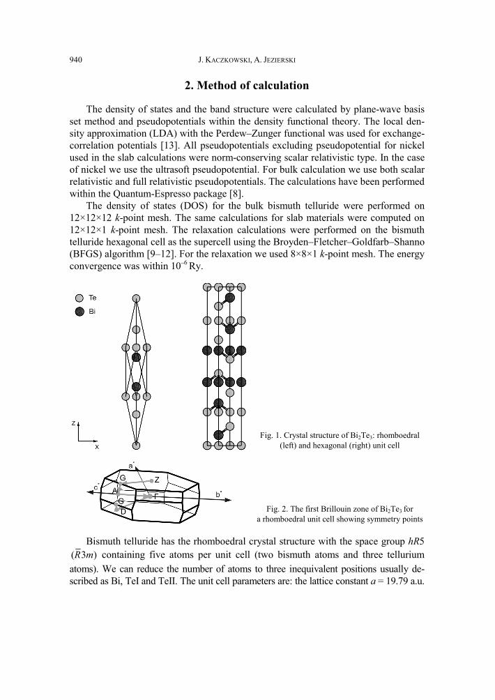
J. KACZKOWSKI, A. JEZIERSKI 940
2. Method of calculation
The density of states and the band structure were calculated by plane-wave basis set method and pseudopotentials within the density functional theory. The local den-sity approximation (LDA) with the Perdew–Zunger functional was used for exchange-correlation potentials [13]. All pseudopotentials excluding pseudopotential for nickel used in the slab calculations were norm-conserving scalar relativistic type. In the case of nickel we use the ultrasoft pseudopotential. For bulk calculation we use both scalar relativistic and full relativistic pseudopotentials. The calculations have been performed within the Quantum-Espresso package [8].
The density of states (DOS) for the bulk bismuth telluride were performed on 12×12×12 k-point mesh. The same calculations for slab materials were computed on 12×12×1 k-point mesh. The relaxation calculations were performed on the bismuth telluride hexagonal cell as the supercell using the Broyden–Fletcher–Goldfarb–Shanno (BFGS) algorithm [9–12]. For the relaxation we used 8×8×1 k-point mesh. The energy convergence was within 10–6 Ry.
Fig. 1. Crystal structure of Bi2Te3: rhomboedral
(left) and hexagonal (right) unit cell
Fig. 2. The first Brillouin zone of Bi2Te3 for
a rhomboedral unit cell showing symmetry points
Bismuth telluride has the rhomboedral crystal structure with the space group hR5 ( 3 )R m containing five atoms per unit cell (two bismuth atoms and three tellurium atoms). We can reduce the number of atoms to three inequivalent positions usually de-scribed as Bi, TeI and TeII. The unit cell parameters are: the lattice constant a = 19.79 a.u.
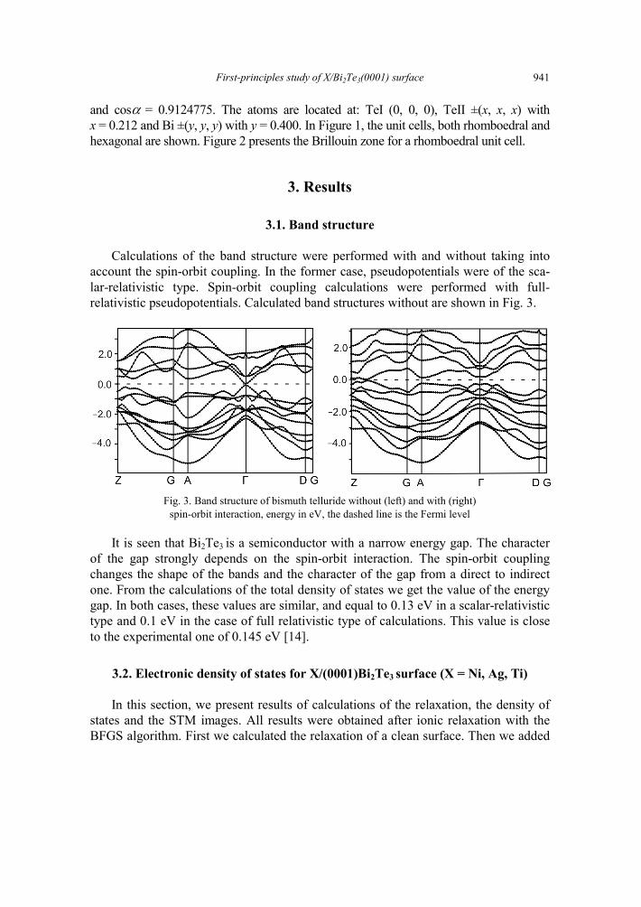
First-principles study of X/Bi2Te3(0001) surface 941
and cosα = 0.9124775. The atoms are located at: TeI (0, 0, 0), TeII ±(x, x, x) with x = 0.212 and Bi ±(y, y, y) with y = 0.400. In Figure 1, the unit cells, both rhomboedral and hexagonal are shown. Figure 2 presents the Brillouin zone for a rhomboedral unit cell.
3. Results
3.1. Band structure
Calculations of the band structure were performed with and without taking into account the spin-orbit coupling. In the former case, pseudopotentials were of the sca-lar-relativistic type. Spin-orbit coupling calculations were performed with full-relativistic pseudopotentials. Calculated band structures without are shown in Fig. 3.
Fig. 3. Band structure of bismuth telluride without (left) and with (right) spin-orbit interaction, energy in eV, the dashed line is the Fermi level
It is seen that Bi2Te3 is a semiconductor with a narrow energy gap. The character of the gap strongly depends on the spin-orbit interaction. The spin-orbit coupling changes the shape of the bands and the character of the gap from a direct to indirect one. From the calculations of the total density of states we get the value of the energy gap. In both cases, these values are similar, and equal to 0.13 eV in a scalar-relativistic type and 0.1 eV in the case of full relativistic type of calculations. This value is close to the experimental one of 0.145 eV [14].
3.2. Electronic density of states for X/(0001)Bi2Te3 surface (X = Ni, Ag, Ti)
In this section, we present results of calculations of the relaxation, the density of states and the STM images. All results were obtained after ionic relaxation with the BFGS algorithm. First we calculated the relaxation of a clean surface. Then we added
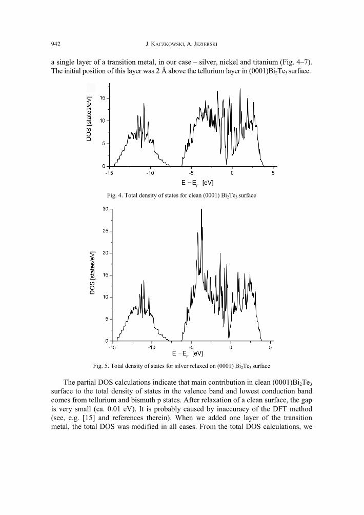
J. KACZKOWSKI, A. JEZIERSKI 942
a single layer of a transition metal, in our case – silver, nickel and titanium (Fig. 4–7). The initial position of this layer was 2 Å above the tellurium layer in (0001)Bi2Te3 surface.
Fig. 4. Total density of states for clean (0001) Bi2Te3 surface
Fig. 5. Total density of states for silver relaxed on (0001) Bi2Te3 surface
The partial DOS calculations indicate that main contribution in clean (0001)Bi2Te3 surface to the total density of states in the valence band and lowest conduction band comes from tellurium and bismuth p states. After relaxation of a clean surface, the gap is very small (ca. 0.01 eV). It is probably caused by inaccuracy of the DFT method (see, e.g. [15] and references therein). When we added one layer of the transition metal, the total DOS was modified in all cases. From the total DOS calculations, we
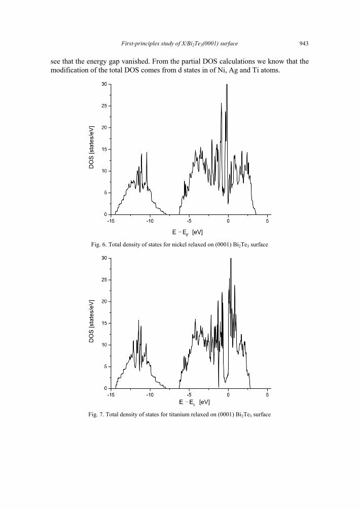
First-principles study of X/Bi2Te3(0001) surface 943
see that the energy gap vanished. From the partial DOS calculations we know that the modification of the total DOS comes from d states in of Ni, Ag and Ti atoms.
Fig. 6. Total density of states for nickel relaxed on (0001) Bi2Te3 surface
Fig. 7. Total density of states for titanium relaxed on (0001) Bi2Te3 surface
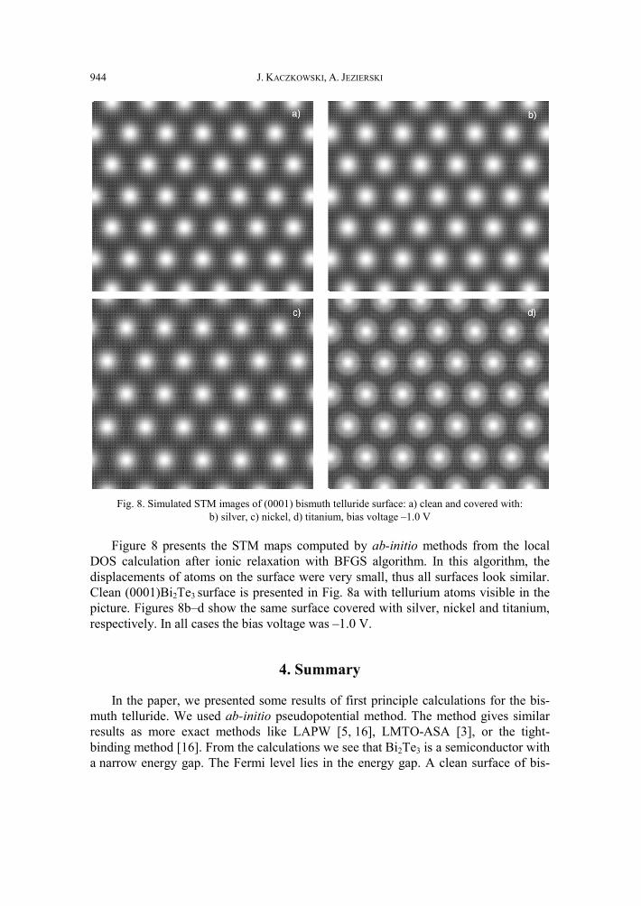
J. KACZKOWSKI, A. JEZIERSKI 944
Fig. 8. Simulated STM images of (0001) bismuth telluride surface: a) clean and covered with: b) silver, c) nickel, d) titanium, bias voltage –1.0 V
Figure 8 presents the STM maps computed by ab-initio methods from the local DOS calculation after ionic relaxation with BFGS algorithm. In this algorithm, the displacements of atoms on the surface were very small, thus all surfaces look similar. Clean (0001)Bi2Te3 surface is presented in Fig. 8a with tellurium atoms visible in the picture. Figures 8b–d show the same surface covered with silver, nickel and titanium, respectively. In all cases the bias voltage was –1.0 V.
4. Summary
In the paper, we presented some results of first principle calculations for the bis-muth telluride. We used ab-initio pseudopotential method. The method gives similar results as more exact methods like LAPW [5, 16], LMTO-ASA [3], or the tight-binding method [16]. From the calculations we see that Bi2Te3 is a semiconductor with a narrow energy gap. The Fermi level lies in the energy gap. A clean surface of bis-
First-principles study of X/Bi2Te3(0001) surface 945
muth telluride covered by one atom layer of metal changes the electronic structure of this material.
Acknowledgements
The work was financed from the science resources as a joint research program within scientific net-work New materials and sensors for optoelectronics, informatics, energetics and medicine.
References
[1] LARSON P., GREANYA V.A., TONJES W.C., LIU RONG, MAHANTI S.D., Phys. Rev. B, 65 (2002), 085108.
[2] YOUN S.J., FREEMAN A.J., Phys. Rev. B, 63 (2001), 085112. [3] MISHRA S.K., SATPATHY S., JEPSEN O., J. Phys. Cond. Matter, 9 (1997), 461. [4] KATSUKI S., J. Phys. Soc. Jap., 26 (1969), 58. [5] LARSON P., MAHANTI S.D., KANATZIDIS M.G., Phys. Rev. B, 61 (2000), 8162. [6] GREANYA V.A., TONJES W.C., LIU R., OLSEN C.G., CHUNG D-Y., KANATZIDIS M.G., Phys. Rev. B, 62
(2000), 16425. [7] UEDA Y., FURUTA A., OKUDA H., NAKATAKE M., SATO H., NAMATAME H., TANIGUCHI M., J. Electron
Spectrosc. Relat. Phen., 101 (1999), 677. [8] BARONI S., DAL CORSO A., DE GIRONCOLI S., GIANNOZZI P., www.pwscf.org or www.quantum
-espresso.org. [9] BROYDEN C.G., J. Inst. Math. Appl., 6 (1970), 76-90.
[10] FLETCHER R., Comp. J., 13 (1970), 317. [11] GOLDFARB D., Math. Comp., 24 (1970), 23. [12] SHANNO D.F., Math. Comp., 24 (1970), 647. [13] PERDEW J.P. AND ZUNGER A., Phys. Rev. B, 23 (1981), 5048. [14] GREENAWAY D.L., HARBEKE G., J. Phys. Chem. Solids, 26 (1965), 1585. [15] POPA V.A., BROCKS G., KELLY P.J., arxiv-org:cond-mat/0507013. [16] THOMAS G.A., RAPKINE D.H., DOVER R.B., MATTHEISS L.F., SUNDER W.A., SCHNEEMEYER L.F.,
WASZCZAK J.V., Phys. Rev. B, 46 (1992), 1553.
Received 16 May 2007 Revised 10 October 2007
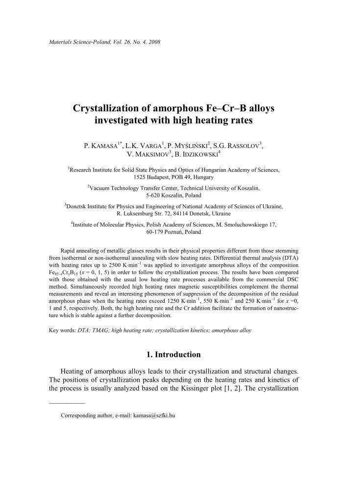
Materials Science-Poland, Vol. 26, No. 4, 2008
Crystallization of amorphous Fe–Cr–B alloys investigated with high heating rates
P. KAMASA1*, L.K. VARGA1, P. MYŚLIŃSKI2, S.G. RASSOLOV3, V. MAKSIMOV3, B. IDZIKOWSKI4
1Research Institute for Solid State Physics and Optics of Hungarian Academy of Sciences, 1525 Budapest, POB 49, Hungary
2Vacuum Technology Transfer Center, Technical University of Koszalin, 5-620 Koszalin, Poland
3Donetsk Institute for Physics and Engineering of National Academy of Sciences of Ukraine, R. Luksemburg Str. 72, 84114 Donetsk, Ukraine
4Institute of Molecular Physics, Polish Academy of Sciences, M. Smoluchowskiego 17, 60-179 Poznań, Poland
Rapid annealing of metallic glasses results in their physical properties different from those stemming from isothermal or non-isothermal annealing with slow heating rates. Differential thermal analysis (DTA) with heating rates up to 2500 K⋅min–1 was applied to investigate amorphous alloys of the composition Fe85–xCrxB15 (x = 0, 1, 5) in order to follow the crystallization process. The results have been compared with those obtained with the usual low heating rate processes available from the commercial DSC method. Simultaneously recorded high heating rates magnetic susceptibilities complement the thermal measurements and reveal an interesting phenomenon of suppression of the decomposition of the residual amorphous phase when the heating rates exceed 1250 K⋅min–1, 550 K⋅min–1 and 250 K⋅min–1 for x =0, 1 and 5, respectively. Both, the high heating rate and the Cr addition facilitate the formation of nanostruc-ture which is stable against a further decomposition.
Key words: DTA; TMAG; high heating rate; crystallization kinetics; amorphous alloy
1. Introduction
Heating of amorphous alloys leads to their crystallization and structural changes. The positions of crystallization peaks depending on the heating rates and kinetics of the process is usually analyzed based on the Kissinger plot [1, 2]. The crystallization __________
Corresponding author, e-mail: [email protected]
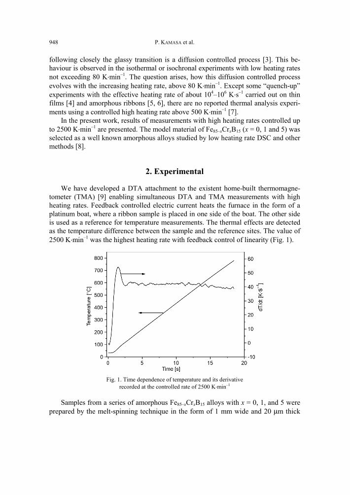
P. KAMASA et al. 948
following closely the glassy transition is a diffusion controlled process [3]. This be-haviour is observed in the isothermal or isochronal experiments with low heating rates not exceeding 80 K⋅min–1. The question arises, how this diffusion controlled process evolves with the increasing heating rate, above 80 K⋅min–1. Except some “quench-up” experiments with the effective heating rate of about 104–106 K⋅s–1 carried out on thin films [4] and amorphous ribbons [5, 6], there are no reported thermal analysis experi-ments using a controlled high heating rate above 500 K⋅min–1 [7].
In the present work, results of measurements with high heating rates controlled up to 2500 K⋅min–1 are presented. The model material of Fe85–xCrxB15 (x = 0, 1 and 5) was selected as a well known amorphous alloys studied by low heating rate DSC and other methods [8].
2. Experimental
We have developed a DTA attachment to the existent home-built thermomagne-tometer (TMA) [9] enabling simultaneous DTA and TMA measurements with high heating rates. Feedback controlled electric current heats the furnace in the form of a platinum boat, where a ribbon sample is placed in one side of the boat. The other side is used as a reference for temperature measurements. The thermal effects are detected as the temperature difference between the sample and the reference sites. The value of 2500 K⋅min–1 was the highest heating rate with feedback control of linearity (Fig. 1).
Fig. 1. Time dependence of temperature and its derivative
recorded at the controlled rate of 2500 K⋅min–1
Samples from a series of amorphous Fe85–xCrxB15 alloys with x = 0, 1, and 5 were prepared by the melt-spinning technique in the form of 1 mm wide and 20 μm thick
Crystallization of amorphous Fe–Cr–B alloys 949
ribbons. The glassy state of the samples was confirmed by the X-ray diffraction meas-urements. The chemical composition of the material was analyzed by the atomic ab-sorption spectroscopy. Two pieces of 10 mm long ribbons (altogether about 3 mg) was used in the DTA experiment. A similar amount of the material cut into 3 mm pieces was used in the DSC experiment.
3. Results
In Figure 2, the DTA and TMAG curves for Fe85B15 amorphous sample obtained using the heating rates between 700 and 2500 K⋅min–1are plotted. The DTA signal was normalized with the heating rate in order to obtain comparable intensities. A two-stage crystallization is observed up to the heating rate of 1250 K⋅min–1. The first exothermic peak (I) in the DTA and the increase of the magnetization value in the TMAG curve are attributed to the precipitation of α-Fe [11]. Next the residual amorphous phase enriches in boron and crystallizes eutecticallly into α-Fe + Fe3B, and this process is observed as a second exothermic peak (II) in the DTA thermograph. A comprehensive analysis of the described above processes can be found elsewhere [8].
Fig. 2. Devitrification process of amorphous Fe85B15 alloy obtained at various heating rates as indicated: DTA curves from the crystallization region (a), and corresponding TMAG curves (b)
With the heating rate increasing above 1250 K⋅min–1, only a smeared out one stage transformation (peak I) is recorded. The same tendency is observed in TMAG meas-urements results. The intensity of the magnetization corresponding to Fe3B formation (peak II) is nearly equal to the first peak (I) of α-Fe precipitation at heating rates be-low 1000 K⋅min–1. Above this value the peak II decreases together with the magnetiza-tion upraise of the first peak. Above 1500 K⋅min–1 heating rate, a smeared out first magnetization peak is only observed (Fig. 2b). Taking the peak temperatures, Tp, at a certain heating rate, q, an ln(q/Tp
2) versus 1/Tp Kissinger plot can be constructed, from which the activation energy of the process can be calculated. The above described
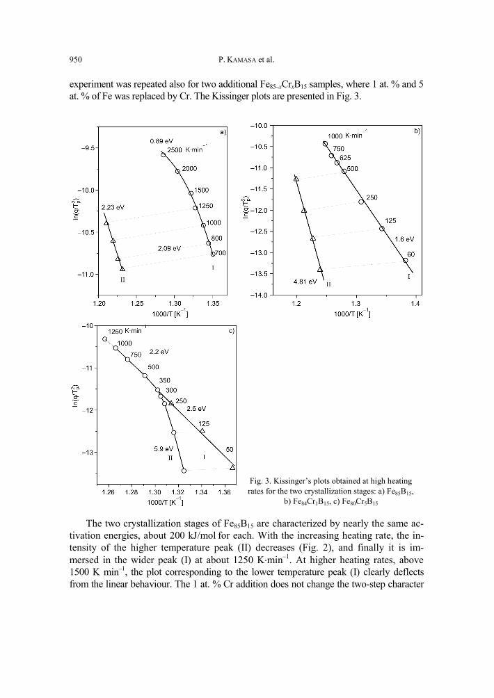
P. KAMASA et al. 950
experiment was repeated also for two additional Fe85–xCrxB15 samples, where 1 at. % and 5 at. % of Fe was replaced by Cr. The Kissinger plots are presented in Fig. 3.
Fig. 3. Kissinger’s plots obtained at high heating rates for the two crystallization stages: a) Fe85B15,
b) Fe84Cr1B15, c) Fe80Cr5B15
The two crystallization stages of Fe85B15 are characterized by nearly the same ac-tivation energies, about 200 kJ/mol for each. With the increasing heating rate, the in-tensity of the higher temperature peak (II) decreases (Fig. 2), and finally it is im-mersed in the wider peak (I) at about 1250 K⋅min–1. At higher heating rates, above 1500 K min–1, the plot corresponding to the lower temperature peak (I) clearly deflects from the linear behaviour. The 1 at. % Cr addition does not change the two-step character
Crystallization of amorphous Fe–Cr–B alloys 951
of the crystallization process; however, the second peak dies out at a much lower heating rate (at about 500 K⋅min–1) than in the case of the original binary alloy Fe85B15.
The evolution of crystallization steps changes drastically when 5 at. % of Fe is re-placed by Cr. The two-stage crystallization is only observed at low heating rates, below 250 K⋅min–1. With the increasing heating rate, the shift of the higher temperature peak (II) is smaller (higher activation energy) than that of the peak (I). At about 300 K/min the two peaks overlap and at higher heating rates only one peak is observed. This peak represents two processes: first, the precipitation of α-Fe, and second, further transformation of the residual amorphous phase. The slope of the overlapped process remained the same as of the process (I), indicating that the precipitation of α-Fe is the determining factor in the cooperative processes of the overlapping crystallization steps. While the activation energy of lower temperature peaks (I) does not change significantly for all three investigated al-loys (ca. 220 kJ·mol–1), the activation energy for higher temperature peaks (II) increases with Cr content. For 1 and 5 at. % Cr contents, the values are 465 and 570 kJ·mol–1, re-spectively, in comparison with the value obtained for the pure binary alloy, amounting to 216 kJ mol–1.
3. Discussion
High heating rates reveal new effects, which may originate directly in the devitri-fication processes. Remarkable is for instance, the deflection from the linearity of the Kissinger plot for the low temperature peak (I) of Fe85B15 above 1250 K·min–1 heating rates. High heating rates can involve higher temperature gradients within the sample, causing a widening in the temperature (time) range of crystallization and shifts the peak temperature, Tp, as well. In the devitrification process the primary crystallization of the α-Fe is a long-range diffusion process, which can be accomplished more easily (with smaller activation energies) at higher temperatures, resulted from the high heat-ing rate shifting. On the other hand, the crystallization of the residual amorphous phase is a short- range diffusion process for which the activation energy is higher and seemingly does not change in the temperature interval of the peak shifting.
Another explanation of this phenomenon could be given by accounting the changes of the boron content in the α-Fe phase. As has been recently shown [12], the concentration of boron in the primary α-Fe increases from 0.14 to 0.39 with increasing the annealing tem-perature of the Fe85B15 metallic glass from 628 to 667 K. According the level rule, the volume fraction occupied by the primary crystals is proportional to [13]:
* 0
1 * xt
c cfc c−=−
where c* and c0 are the matrix concentrations at the interface and far from it, respec-tively, and cxt is the concentration of the crystallite precipitate. It is easy to show that at cxt → c0 (i.e., to 0.15) the volume fraction of the α-phase approaches 1. In fact, the sample of amorphous Fe85B15 alloy crystallized at the heating rate of about 104 K·s–1
P. KAMASA et al. 952
had a single phase structure consisting of nanoscale (10–30 nm) grains of supersatu-rated solid solution of boron in α-Fe [6]. Analysis of primary crystallization kinetics at high heating rates and structure of the partially (nanocrystalline states) and fully crys-tallized samples confirm this scenario of structural changes.
4. Conclusions
The behaviour of the crystallization steps in function of heating rates and Cr con-tent revealed that the decomposition of the residual amorphous phase is strictly de-pendent on the evaluation of the first stage of the devitrification process. The calcula-tions of activation energies of thermally activated reactions studied during linear heating confirm validity of model-free isoconversion methods which use approxima-tions of the temperature integral [14]. As in the present case, these methods neglect the temperature integral at the start of the linear heating. A high rate of heat treatment may produce various nanostructures, not available at heat treatment with conventional low heating rates. This may cause disappearance of the higher temperature peak (II) ob-served with the increasing heating rate. XRD and TEM measurements (not presented here) confirm two different dynamics of structural changes.
References [1] KISSINGER H.E., J. Res. Nat. Bureau Standards, 57 (1956), 217. [2] KISSINGER H.E., Anal. Chem., 29 (1957), 1702. [3] NAKAJIMA T., KITA E., INO H., J. Mater. Sci., 23 (1988), 1279. [4] ADAMOVSKY S., SCHICK C., Thermochim. Acta, 415 (2004), 1. [5] ZAŁUSKA A., MATYJA H., J. Mater. Sci. Lett., 2 (1983), 729. [6] ABROSIMOVA G.E., ARONIN A.S., STELMUH V.A., Solid State Phys., 33 (1991), 3570. [7] ICHITSUBO T., MATSUBARA E., NUMAKURA H., TANAKA K., NISHIYAMA N., TARUMI R., Phys. Rev. B,
72 (2005), 052201. [8] KÖSTER U., HEROLD U., [in:] Glassy Metals I, H.J. Güntherodt, H. Beck (Eds), Springer, New York,
1981, 230. [9] KAMASA P., VARGA L.K., KISDI-KOSZÓ É., VANDLIK J. [in:] P. Duhaj, P. Mrafko, P. Svec (Eds.),
Suppl. to the Proc. 9th Int. Conf. on Rapidly Quenched and Metastable Alloys, Bratislava (Slovakia), 1996, Elsevier, Amsterdam, 1997, 280.
[10] KISDI-KOSZÓ É., KISS L.F., VARGA L.K., KAMASA P., Mater. Sci. Eng. A, 226–228 (1997), 689. [11] KAMASA P., BUZIN A., PYDA M., KOVAC J., CZIRÁKI Á., LOVAS A., BAKONYI I., J. Magn. Magn. Ma-
ter, 257 (2003), 274. [12] TKATCH V.I., RASSOLOV S.G., MOISEEVA T.N., POPOV V.V., J. Non-Cryst. Solids, 1351, (2005), 1658. [13] CLAVAGUERA-MORA M.T., CLAVAGUERA N., CRESPO D., PRADELL T., Progr. Mater. Sci., 47 (2002), 559. [14] STARINK M.J., Thermochim. Acta, 404 (2003), 163.
Received 31 May 2007 Revised 22 December 2007
Materials Science-Poland, Vol. 26, No. 4, 2008
Properties of GdFeAl ternary compound in two crystallographic structures
M. KLIMCZAK1*, E. TALIK1, J. JAROSZ1, T. MYDLARZ2
1Institute of Physics, University of Silesia, Uniwersytecka 4, 40-007 Katowice, Poland 2International Laboratory of High Magnetic Fields
and Low Temperatures, Gajowicka 95, 53-529 Wrocław, Poland
Properties of the GdFeAl compounds crystallizing in the cubic MgCu2-type structure as well as in hex-agonal MgZn2-type structure have been compared. The electrical resistivity, ac susceptibility and magnetization in function of temperature revealed relatively high magnetic ordering temperature, ca. 200 K. The differences in magnetization were observed for samples crystallizing in two different crystallographic structures. The magnet-ic moments measured at 4.2 K and up to140 kOe are very far from the value of the magnetic moment of a free Gd ion. The magnetic moments of cubic and hexagonal phases are 1.1 μB and 1.7 μB, respectively.
Key words: rare earth transition metal compounds; lattice parameters; magnetization; electrical resistivity
1. Introduction
Magnetic refrigeration technology is at present one of the most studied research issues in advanced refrigeration systems [1]. Magnetic refrigeration, based on magnetocaloric effect (MCE), offers the prospect of an energy-efficient and environment friendly alterna-tive to the common vapour-cycle refrigeration technology in use today [2, 3]. Materials based on gadolinium are prospective for applications in magnetic refrigeration cycles. Recently, interest in other magnetocaloric materials such as e.g. RM2 (M = Al, Co, Ni), MnFe(P1–xAsx), Mn(As1–xSbx), La(Fe13–xSix) has also been reported [4, 5]. These new mate-rials have important significance for magnetic cooling.
Recently, magnetic and magnetocaloric properties of GdFeSi have been investi-gated as a part of research concerning the development of new materials for magnetic refrigeration devices [6]. GdFeSi polycrystalline sample crystallizes in the Cu2Sb type structure and orders feromagnetically at 118 K. However, a high magnetic field em-ployed together with the large temperature span for the refrigerant capacity integration prevents any industrial applicability. The intermetallic ternary compounds of the RTX __________
*Corresponding author, e-mail: [email protected]
M. KLIMCZAK et al. 954
type, consisting of a rare earth R, transition metal T and a p element X exhibit an enormously rich variety of crystallographic structures and magnetic properties. Some of these compounds could exist in various crystallographic structures. The well known example is GdPdAl (TiNiSi or ZrNiAl) [7]. Usually, the type of assumed structure depends on the way in which it was synthesized. A well known example of such a compound is GdPdAl which crystallizes in TiNiSi type structure, when cooled slow-ly or in ZrNiAl-type structure, when quenched [7]. Presence of high pressure during the crystallization can change the ZrNiAl-type structure of RCuAl and RNiAl to a more densely packed MgCu2 structure (the former compound) and to MgZn2 type (the latter one) of the Laves phase [8]. Recently, properties of GdPdX (X = Al, Si, Ga, Ge, In, Si) compounds have been extensively examined [9]. The magnetic ordering tem-peratures of the GdPdX compounds are close 30 K, except for GdPdIn. This latter has much higher ordering temperature of about 100 K.
Due to the lack of information relevant to the intermetallic compound GdFeAl, a complete research has been performed. In this paper, we report differences between the crystal structures and magnetic properties of two forms of the GdFeAl compound. Moreover, the electrical resistivity and ac magnetic susceptibility measurements for the cubic phase of the GdFeAl are presented.
2. Experimental
Polycrystalline GdFeAl intermetallic compounds were prepared by arc melting on a cool copper plate under the argon atmosphere from the stoichiometric amounts of high purity constituents. The obtained samples were divided into two parts, then one of them was annealed at 1000 K for one day and then cooled slowly, and the other ones were annealed and quenched. The obtained compounds were identified by the X-ray power diffraction with the CuKα radiation using a Siemens D-5000 diffractometer. For the quenched sample the lattice parameters were obtained at room temperature, while for the annealed one the lattice constants were determined on decreasing the temperature from 300 K to 10 K and then increasing to 300 K again.
Measurements of the magnetization were performed in a static magnetic field up to 140 kOe at temperatures from 4.2 to 300 K. The electrical resistivity measurements were performed by a conventional four-point technique using 300 mA dc current in the temperature range 4.2–300 K. The ac magnetic susceptibility was measured at the frequency of 1 kHz in the temperature range 4.2–300 K. The ac magnetic field of 150 mOe was applied.
3. Results and discussion
The X-ray diffraction examination confirmed the hexagonal MgZn2 type of the crystal structure for the annealed and quenched sample, and revealed the cubic MgCu2
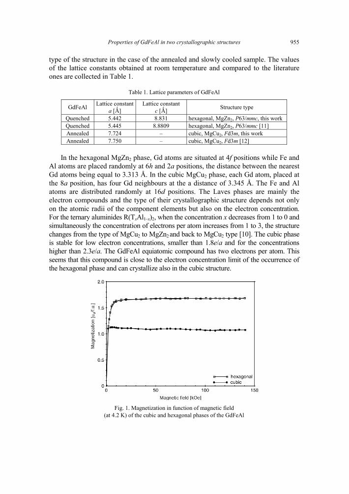
Properties of GdFeAl in two crystallographic structures 955
type of the structure in the case of the annealed and slowly cooled sample. The values of the lattice constants obtained at room temperature and compared to the literature ones are collected in Table 1.
Table 1. Lattice parameters of GdFeAl
GdFeAl Lattice constant a [Ǻ]
Lattice constant c [Ǻ] Structure type
Quenched 5.442 8.831 hexagonal, MgZn2, P63/mmc, this work Quenched 5.445 8.8809 hexagonal, MgZn2, P63/mmc [11] Annealed 7.724 – cubic, MgCu2, Fd3m, this work Annealed 7.750 – cubic, MgCu2, Fd3m [12]
In the hexagonal MgZn2 phase, Gd atoms are situated at 4f positions while Fe and
Al atoms are placed randomly at 6h and 2a positions, the distance between the nearest Gd atoms being equal to 3.313 Å. In the cubic MgCu2 phase, each Gd atom, placed at the 8a position, has four Gd neighbours at the a distance of 3.345 Å. The Fe and Al atoms are distributed randomly at 16d positions. The Laves phases are mainly the electron compounds and the type of their crystallographic structure depends not only on the atomic radii of the component elements but also on the electron concentration. For the ternary aluminides R(TxAl1–x)2, when the concentration x decreases from 1 to 0 and simultaneously the concentration of electrons per atom increases from 1 to 3, the structure changes from the type of MgCu2 to MgZn2 and back to MgCu2 type [10]. The cubic phase is stable for low electron concentrations, smaller than 1.8e/a and for the concentrations higher than 2.3e/a. The GdFeAl equiatomic compound has two electrons per atom. This seems that this compound is close to the electron concentration limit of the occurrence of the hexagonal phase and can crystallize also in the cubic structure.
Fig. 1. Magnetization in function of magnetic field
(at 4.2 K) of the cubic and hexagonal phases of the GdFeAl
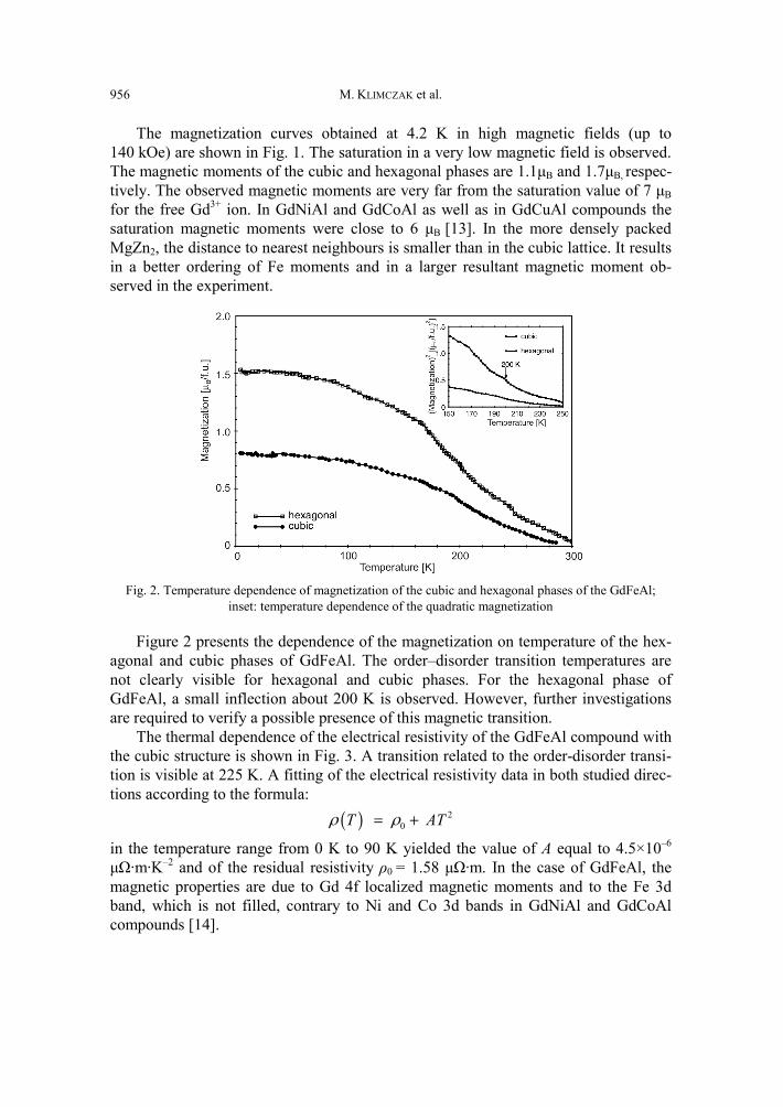
M. KLIMCZAK et al. 956
The magnetization curves obtained at 4.2 K in high magnetic fields (up to 140 kOe) are shown in Fig. 1. The saturation in a very low magnetic field is observed. The magnetic moments of the cubic and hexagonal phases are 1.1μB and 1.7μB, respec-tively. The observed magnetic moments are very far from the saturation value of 7 μB for the free Gd3+ ion. In GdNiAl and GdCoAl as well as in GdCuAl compounds the saturation magnetic moments were close to 6 μB [13]. In the more densely packed MgZn2, the distance to nearest neighbours is smaller than in the cubic lattice. It results in a better ordering of Fe moments and in a larger resultant magnetic moment ob-served in the experiment.
Fig. 2. Temperature dependence of magnetization of the cubic and hexagonal phases of the GdFeAl;
inset: temperature dependence of the quadratic magnetization
Figure 2 presents the dependence of the magnetization on temperature of the hex-agonal and cubic phases of GdFeAl. The order–disorder transition temperatures are not clearly visible for hexagonal and cubic phases. For the hexagonal phase of GdFeAl, a small inflection about 200 K is observed. However, further investigations are required to verify a possible presence of this magnetic transition.
The thermal dependence of the electrical resistivity of the GdFeAl compound with the cubic structure is shown in Fig. 3. A transition related to the order-disorder transi-tion is visible at 225 K. A fitting of the electrical resistivity data in both studied direc-tions according to the formula:
( ) 20 T ATρ ρ= +
in the temperature range from 0 K to 90 K yielded the value of A equal to 4.5×10⁻⁶ μΩ·m·K–2 and of the residual resistivity ρ0 = 1.58 μΩ·m. In the case of GdFeAl, the magnetic properties are due to Gd 4f localized magnetic moments and to the Fe 3d band, which is not filled, contrary to Ni and Co 3d bands in GdNiAl and GdCoAl compounds [14].
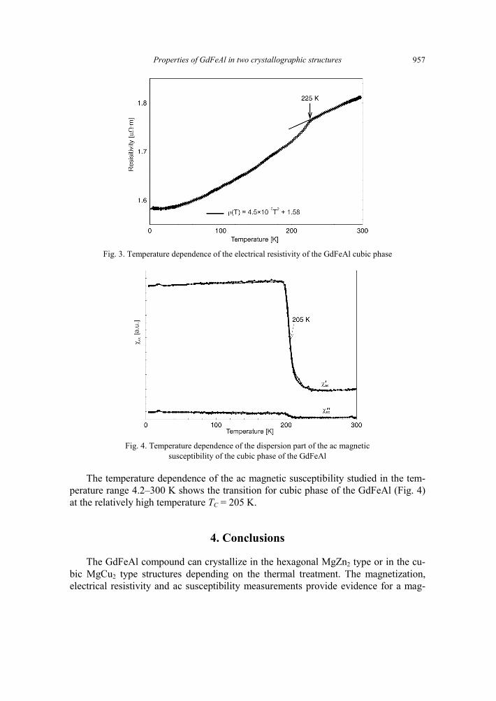
Properties of GdFeAl in two crystallographic structures 957
Fig. 3. Temperature dependence of the electrical resistivity of the GdFeAl cubic phase
Fig. 4. Temperature dependence of the dispersion part of the ac magnetic
susceptibility of the cubic phase of the GdFeAl
The temperature dependence of the ac magnetic susceptibility studied in the tem-perature range 4.2–300 K shows the transition for cubic phase of the GdFeAl (Fig. 4) at the relatively high temperature TC = 205 K.
4. Conclusions
The GdFeAl compound can crystallize in the hexagonal MgZn2 type or in the cu-bic MgCu2 type structures depending on the thermal treatment. The magnetization, electrical resistivity and ac susceptibility measurements provide evidence for a mag-
M. KLIMCZAK et al. 958
netic transition at about 200 K. The GdFeAl compounds contain the Gd atoms with localized 4f magnetic moments together with the Fe 3d atoms and non-magnetic alu-minum. The influence of iron on the properties of the compounds under investigation needs further examinations.
Acknowledgements
The work is supported by the Polish State Committee for Scientific Research (KBN) within Grant No. N202 149 31/2727. One of the authors (m. Klimczak) is the UPGOW (Uniwersytet Partnerem Go-spodarki Opartej na Wiedzy) scholarship holder.
References
[1] YU B.F., GAO Q., ZHANG B., MENG X.Z., CHEN Z., Int. J. Refrigeration, 26 (2003), 622. [2] PECHARSKY V.K., GSCHNEIDER JR K.A., J. Appl. Phys., 85 (1999), 5365. [3] GSCHNEIDER JR K.A., PECHARSKY V.K., Annu. Rev. Mater. Sci., 30 (2000), 387 [4] GSCHNEIDNER JR K.A., PECHARSKY V.K., TSOKOL A.O., Rep. Prog. Phys., 68 (2005), 1479. [5] BRÜCK E., J. Phys. D Appl. Phys., 38 (2005), R381. [6] NAPOLETANO M., CANEPA F., MANFRINETTI P., MERLO F., J. Mater. Chem., 10 (2000), 1663. [7] HULLIGER F., J. Alloys Comp., 218 (1995), 44. [8] TSVYASHCHENKO A.V., FOMICHEVA L.M., J. Less Common Met., 135 (1987), L9. [9] TALIK E., KUSZ J., HOFMEISTER W., MATLAK M., SKUTECKA M., KLIMCZAK M., J. Alloys Comp.,
423 (2006), 47. [10] ŚLEBARSKI A., J. Magn. Magn. Mater., 66 (1987), 107. [11] BUSCHOW K.H.J., J. Magn. Magn. Mater., 38 (1983), 91. [12] OESTERREICHER H., J. Less Common Met., 13 (1967), L9. [13] JAROSZ J., TALIK E., MYDLARZ T., KUSZ J., BÖHM H., WINIARSKI A., J. Magn. Magn. Mater., 208
(2000), 169. [14] JAROSZ J., TALIK E., J. Alloys Compounds, 317 (2001), 385.
Received 7 May 2007 Revised 26 June 2007
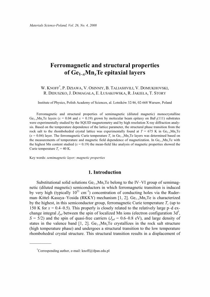
Materials Science-Poland, Vol. 26, No. 4, 2008
Ferromagnetic and structural properties of Ge1–xMnxTe epitaxial layers
W. KNOFF*, P. DZIAWA, V. OSINNIY, B. TALIASHVILI, V. DOMUKHOVSKI, R. DIDUSZKO, J. DOMAGAŁA, E. ŁUSAKOWSKA, R. JAKIEŁA, T. STORY
Institute of Physics, Polish Academy of Sciences, al. Lotników 32/46, 02-668 Warsaw, Poland
Ferromagnetic and structural properties of semimagnetic (diluted magnetic) monocrystalline Ge1–xMnxTe layers (x = 0.04 and x = 0.19) grown by molecular beam epitaxy on BaF2(111) substrates were experimentally studied by the SQUID magnetometry and by high resolution X-ray diffraction analy-sis. Based on the temperature dependence of the lattice parameter, the structural phase transition from the rock salt to the rhombohedral crystal lattice was experimentally found at T = 675 K in Ge1–xMnxTe (x = 0.04) layer. The ferromagnetic Curie temperature Tc in Ge1–xMnxTe layers was determined based on the measurements of temperature and magnetic field dependence of magnetization. In Ge1–xMnxTe with the highest Mn content studied (x = 0.19) the mean-field like analysis of magnetic properties showed the Curie temperature Tc = 40 K.
Key words: semimagnetic layer; magnetic properties
1. Introduction
Substitutional solid solutions Ge1–xMnxTe belong to the IV–VI group of semimag-netic (diluted magnetic) semiconductors in which ferromagnetic transition is induced by very high (typically 1021 cm–3) concentration of conducting holes via the Ruder-man–Kittel–Kasuya–Yosida (RKKY) mechanism [1, 2]. Ge1–xMnxTe is characterized by the highest, in this semiconductor group, ferromagnetic Curie temperature Tc (up to 150 K for x = 0.4–0.5). This properly is closely related to the relatively large p–d ex-change integral Jpd between the spin of localized Mn ions (electron configuration 3d5, S = 5/2) and the spin of quasi-free carriers (Jpd = 0.6–0.8 eV), and large density of states in the valence band [1, 2]. Ge1–xMnxTe crystallizes in the rock salt structure (high temperature phase) and undergoes a structural transition to the low temperature rhombohedral crystal structure. This structural transition results in a displacement of
__________
*Corresponding author, e-mail: [email protected]
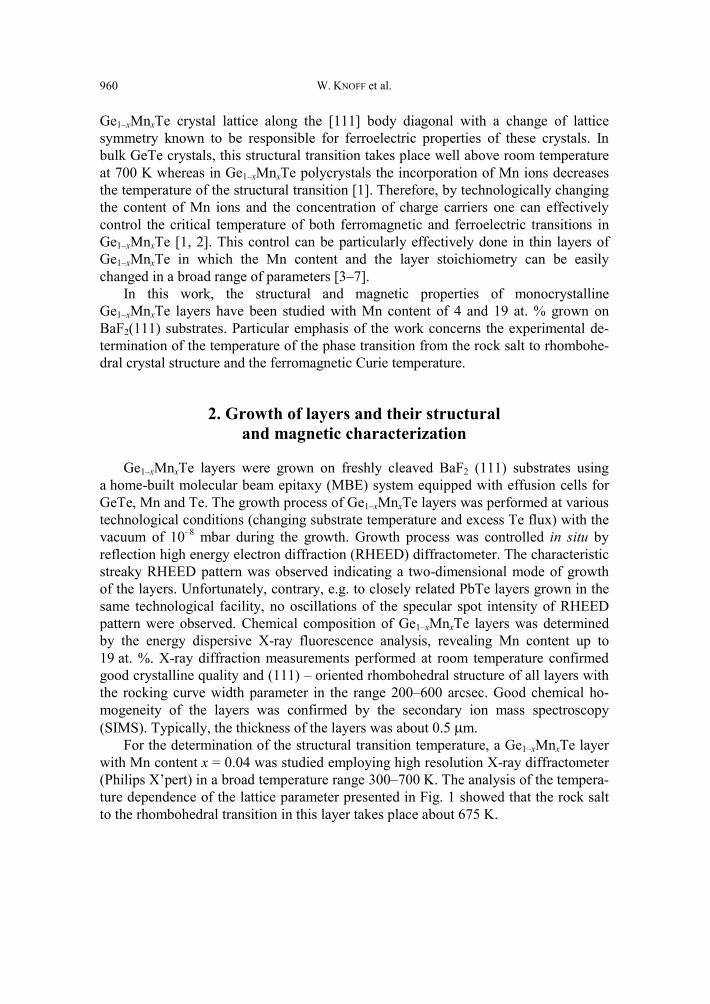
W. KNOFF et al. 960
Ge1–xMnxTe crystal lattice along the [111] body diagonal with a change of lattice symmetry known to be responsible for ferroelectric properties of these crystals. In bulk GeTe crystals, this structural transition takes place well above room temperature at 700 K whereas in Ge1–xMnxTe polycrystals the incorporation of Mn ions decreases the temperature of the structural transition [1]. Therefore, by technologically changing the content of Mn ions and the concentration of charge carriers one can effectively control the critical temperature of both ferromagnetic and ferroelectric transitions in Ge1–xMnxTe [1, 2]. This control can be particularly effectively done in thin layers of Ge1–xMnxTe in which the Mn content and the layer stoichiometry can be easily changed in a broad range of parameters [3–7].
In this work, the structural and magnetic properties of monocrystalline Ge1–xMnxTe layers have been studied with Mn content of 4 and 19 at. % grown on BaF2(111) substrates. Particular emphasis of the work concerns the experimental de-termination of the temperature of the phase transition from the rock salt to rhombohe-dral crystal structure and the ferromagnetic Curie temperature.
2. Growth of layers and their structural and magnetic characterization
Ge1–xMnxTe layers were grown on freshly cleaved BaF2 (111) substrates using a home-built molecular beam epitaxy (MBE) system equipped with effusion cells for GeTe, Mn and Te. The growth process of Ge1–xMnxTe layers was performed at various technological conditions (changing substrate temperature and excess Te flux) with the vacuum of 10–8 mbar during the growth. Growth process was controlled in situ by reflection high energy electron diffraction (RHEED) diffractometer. The characteristic streaky RHEED pattern was observed indicating a two-dimensional mode of growth of the layers. Unfortunately, contrary, e.g. to closely related PbTe layers grown in the same technological facility, no oscillations of the specular spot intensity of RHEED pattern were observed. Chemical composition of Ge1–xMnxTe layers was determined by the energy dispersive X-ray fluorescence analysis, revealing Mn content up to 19 at. %. X-ray diffraction measurements performed at room temperature confirmed good crystalline quality and (111) – oriented rhombohedral structure of all layers with the rocking curve width parameter in the range 200–600 arcsec. Good chemical ho-mogeneity of the layers was confirmed by the secondary ion mass spectroscopy (SIMS). Typically, the thickness of the layers was about 0.5 μm.
For the determination of the structural transition temperature, a Ge1–xMnxTe layer with Mn content x = 0.04 was studied employing high resolution X-ray diffractometer (Philips X’pert) in a broad temperature range 300–700 K. The analysis of the tempera-ture dependence of the lattice parameter presented in Fig. 1 showed that the rock salt to the rhombohedral transition in this layer takes place about 675 K.
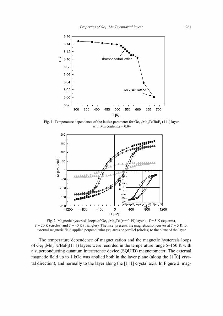
Properties of Ge1–xMnxTe epitaxial layers 961
Fig. 1. Temperature dependence of the lattice parameter for Ge1–xMnxTe/BaF2 (111) layer with Mn content x = 0.04
Fig. 2. Magnetic hysteresis loops of Ge1–xMnxTe (x = 0.19) layer at T = 5 K (squares),
T = 20 K (circles) and T = 40 K (triangles). The inset presents the magnetization curves at T = 5 K for external magnetic field applied perpendicular (squares) or parallel (circles) to the plane of the layer
The temperature dependence of magnetization and the magnetic hysteresis loops of Ge1–xMnxTe/BaF2(111) layers were recorded in the temperature range 5–150 K with a superconducting quantum interference device (SQUID) magnetometer. The external magnetic field up to 1 kOe was applied both in the layer plane (along the [1 10] crys-tal direction), and normally to the layer along the [111] crystal axis. In Figure 2, mag-
W. KNOFF et al. 962
netic hysteresis loops are presented for a Ge1–xMnxTe layer with the highest Mn con-tent studied, x = 0.19. This layer shows the ferromagnetic transition at ca. 40 K as evidenced by the temperature dependence of magnetization presented in Fig. 3.
Fig. 3 Temperature dependence of magnetization for Ge1–xMnxTe layer with Mn content x = 0.19.
The external magnetic field applied either perpendicular (squares) or parallel (circles) to the plane of the layer. The inset shows mean field model estimation of the Curie temperature from the M2(T) plot
We note that the temperature dependence of magnetization of this layer shows a mean-filed-like character (see the inset in Fig. 3) what is in contrast to previously stu-died layers revealing a very broad magnetic transition region [7]. In the inset in Fig. 2 as well as in Fig. 3, a comparison is presented of the temperature and magnetic field de-pendences of the magnetization of Ge1–xMnxTe layer measured with various orientations of magnetic field with respect to the layer (in-plane versus out-of-plane geometry).
3. Discussion and conclusions
Although the experimental data presented in Figs. 2 and 3 indicate a certain ten-dency of the Ge1–xMnxTe/BaF2 layer to exhibit normal to the plane easy axis, this ef-fect is much smaller as compared to previously studied layers, for which a clear nor-mal to the plane easy axis was experimentally found in both SQUID and ferromagnetic resonance studies [7]. As the Hall effect measurements of the layer with x = 0.19 indicated a very high carrier concentration (about 5×1021 cm–3), it suggests that the variety of the magnetic field and temperature characteristics of magnetization observed in Ge1–xMnxTe/BaF2 layers is primarily governed by their electrical homo-geneity and the concentration of carriers, with a negligible effect of possible irregulari-ties in Mn ions distribution. The magnetization observed in the layer with x = 0.19 is
Properties of Ge1–xMnxTe epitaxial layers 963
close to saturation value expected for 5 Bohr magnetons per Mn2+ ion (160 emu/cm3). However, experimentally we do not see a true magnetic saturation in fields available in our magnetometer (below 2 kOe).
In conclusion, we experimentally examined the crystal structure as well as the magnetic field and temperature dependences of magnetization of semimagnetic (di-luted magnetic) semiconductor layers of Ge1–xMnxTe grown by MBE on BaF2(111) substrates. The structural transition from the rock salt to rhombohedral structure was analyzed based on the temperature dependence of lattice parameter. In the layer with the highest Mn content (x = 0.19) and carrier concentration of the order of 1021 cm–3 the ferromagnetic transition was observed at Tc = 40 K.
Acknowledgements
This work was supported by the research project 0992/T02/2007/32 of the Ministry of Science and Higher Education (Poland) granted for the period 2007-2010.
References
[1] COCHRANE R.W., PLISCHKE M., STROM-OLSEN J.O., Phys. Rev. B, 9 (1974), 3013. [2] STORY T., [in:] Lead Chalcogenides. Physics and Applications, D.R. Khokhlov (Ed.), Taylor and
Francis, New York, 2003, p. 385. [3] FUKUMA Y., TANAKA K., ASADA H., KOYANAGI T., J. Magn. Magn. Mater., 310 (2007). [4] CHEN W.Q., TEO K.L., JALIL M.B.A., LIEW T., J. Appl. Phys., 99 (2006), 08D515. [5] FUKUMA Y., ASADA H., NISHIMURA N., KOYANAGI T., J. Appl. Phys., 93 (2003) 4034. [6] FUKUMA Y., ARIFUKU M., ASADA H., KOYANAGI T., J. Appl. Phys., 97 ( 2005) 073910. [7] KNOFF W., DZIAWA P., OSINNIY V., TALIASHVILI B., DOMUKHOVSKI V., ŁUSAKOWSKA E., ŚWIATEK K.,
STORY T., Mater. Sci.-Poland, 25, (2007), 295.
Received 7 May 2007 Revised 30 May 2007
Materials Science-Poland, Vol. 26, No. 4, 2008
Electronic miniband formation in a two-dimensional semiconductor superlattice
J. W. KŁOS*, M. KRAWCZYK
Surface Physics Division, Faculty of Physics, Adam Mickiewicz University, ul. Umultowska 85, 61-614 Poznań, Poland
A system of periodically arranged uniform rods has been investigated, regarded as a two-dimensional superlattice. The assumed arrangement of rods within a supercell allows one to express the two-dimensional effective potential as a sum of two terms depending only on either x or y coordinate. The structure consists of two square lattices of square rods embedded in the matrix material. Rods in one lattice act as potential barriers for electrons, and those in the other as potential wells. The separation of the effective potential is shown not to imply Hamiltonian separation in the envelope function approxima-tion. The energy spectra of the conduction band are computed for the numerical solution as well as for the analytical one, the latter wrongly assuming the separation of the Hamiltonian. The band structures com-puted in the two cases differ in band position and width.
Key words: 2D superlattice; electronic states; photovoltaic cell
1. Introduction
Electronic superlattices are a sort of artificial materials that can be of use in de-signing third generation solar cells [1]. Special attention is paid to quantum dot super-lattices, allowing increased efficiency of light to voltage conversion due to increased photovoltage as well as photocurrent [2]. Increased photovoltage is achieved thanks to the possibility of electron transitions between successive minibands in the superlattice structure, with multiple absorption of low-energy photons [3]. Moreover, in quantum dots, in which partial carrier binding occurs, thermalization time becomes significantly longer [4, 5]. This allows one to capture hot carriers before their relaxation to the mi-niband bottom with phonon emission [6]. The increased photocurrent in a superlattice solar cell is due to impact ionization (reverse Auger effect) consisting in the creation of an extra electron-hole pair at the cost of hot electron energy [7].
__________
*Corresponding author, e-mail:[email protected]
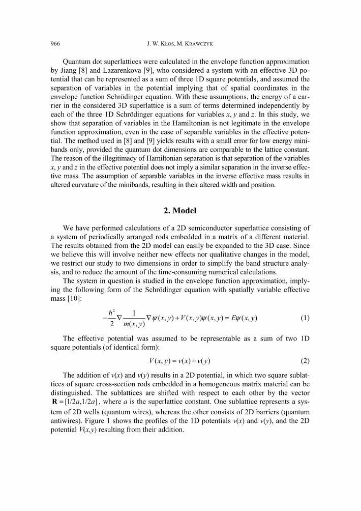
J. W. KŁOS, M. KRAWCZYK 966
Quantum dot superlattices were calculated in the envelope function approximation by Jiang [8] and Lazarenkova [9], who considered a system with an effective 3D po-tential that can be represented as a sum of three 1D square potentials, and assumed the separation of variables in the potential implying that of spatial coordinates in the envelope function Schrödinger equation. With these assumptions, the energy of a car-rier in the considered 3D superlattice is a sum of terms determined independently by each of the three 1D Schrödinger equations for variables x, y and z. In this study, we show that separation of variables in the Hamiltonian is not legitimate in the envelope function approximation, even in the case of separable variables in the effective poten-tial. The method used in [8] and [9] yields results with a small error for low energy mini-bands only, provided the quantum dot dimensions are comparable to the lattice constant. The reason of the illegitimacy of Hamiltonian separation is that separation of the variables x, y and z in the effective potential does not imply a similar separation in the inverse effec-tive mass. The assumption of separable variables in the inverse effective mass results in altered curvature of the minibands, resulting in their altered width and position.
2. Model
We have performed calculations of a 2D semiconductor superlattice consisting of a system of periodically arranged rods embedded in a matrix of a different material. The results obtained from the 2D model can easily be expanded to the 3D case. Since we believe this will involve neither new effects nor qualitative changes in the model, we restrict our study to two dimensions in order to simplify the band structure analy-sis, and to reduce the amount of the time-consuming numerical calculations.
The system in question is studied in the envelope function approximation, imply-ing the following form of the Schrödinger equation with spatially variable effective mass [10]:
2 1 ( , ) ( , ) ( , ) ( , )
2 ( , )x y V x y x y E x y
m x yψ ψ ψ− ∇ ∇ + = (1)
The effective potential was assumed to be representable as a sum of two 1D square potentials (of identical form):
( , ) ( ) ( )V x y v x v y= + (2)
The addition of v(x) and v(y) results in a 2D potential, in which two square sublat-tices of square cross-section rods embedded in a homogeneous matrix material can be distinguished. The sublattices are shifted with respect to each other by the vector
[1/2 ,1/2 ]a a=R , where a is the superlattice constant. One sublattice represents a sys-tem of 2D wells (quantum wires), whereas the other consists of 2D barriers (quantum antiwires). Figure 1 shows the profiles of the 1D potentials v(x) and v(y), and the 2D potential V(x,y) resulting from their addition.
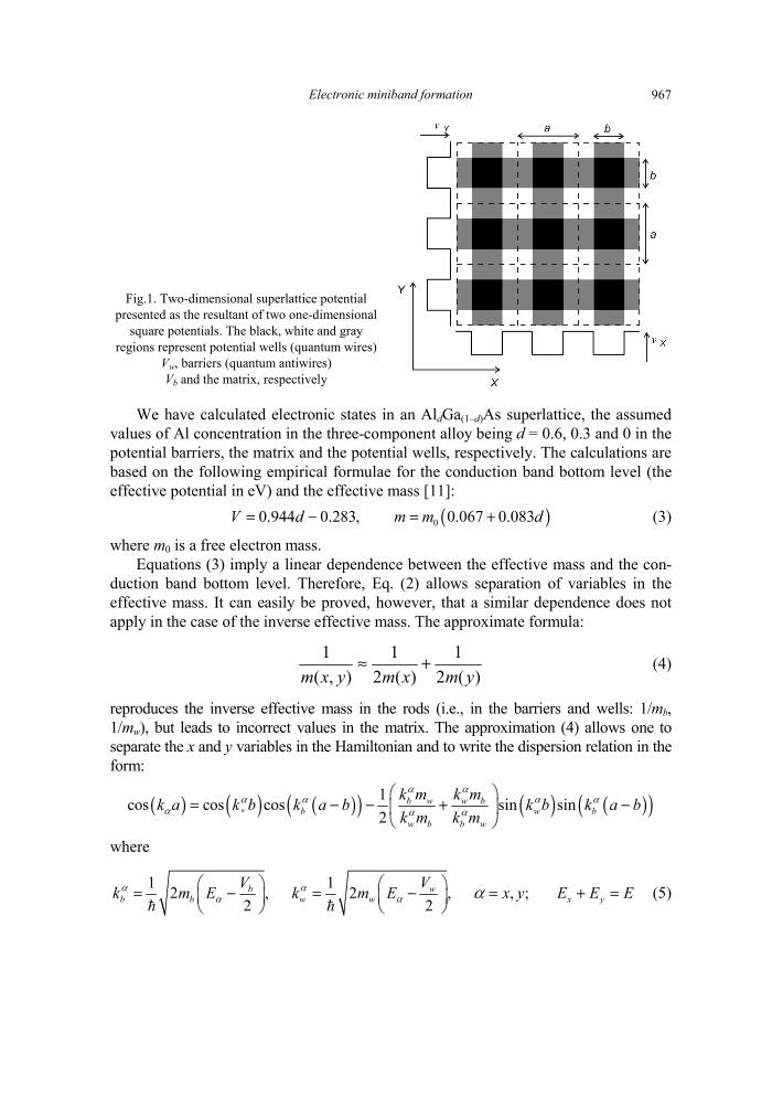
Electronic miniband formation 967
Fig.1. Two-dimensional superlattice potential presented as the resultant of two one-dimensional
square potentials. The black, white and gray regions represent potential wells (quantum wires)
Vw, barriers (quantum antiwires) Vb and the matrix, respectively
We have calculated electronic states in an AldGa(1–d)As superlattice, the assumed values of Al concentration in the three-component alloy being d = 0.6, 0.3 and 0 in the potential barriers, the matrix and the potential wells, respectively. The calculations are based on the following empirical formulae for the conduction band bottom level (the effective potential in eV) and the effective mass [11]: 0.944 0.283,V d= − ( )0 0.067 0.083m m d= + (3)
where m0 is a free electron mass. Equations (3) imply a linear dependence between the effective mass and the con-
duction band bottom level. Therefore, Eq. (2) allows separation of variables in the effective mass. It can easily be proved, however, that a similar dependence does not apply in the case of the inverse effective mass. The approximate formula:
)(2
1)(2
1),(
1ymxmyxm
+≈ (4)
reproduces the inverse effective mass in the rods (i.e., in the barriers and wells: 1/mb, 1/mw), but leads to incorrect values in the matrix. The approximation (4) allows one to separate the x and y variables in the Hamiltonian and to write the dispersion relation in the form:
( ) ( ) ( )( ) ( ) ( )( )1cos cos cos sin sin2w
b w w bb w b
w b b w
k m k mk a k b k a b k b k a bk m k m
α αα α α α
α α α
⎛ ⎞= − − + −⎜ ⎟
⎝ ⎠
where
1 12 , 2 , , ;2 2b w
b b w w x yV Vk m E k m E x y E E Eα α
α α α⎛ ⎞ ⎛ ⎞= − = − = + =⎜ ⎟ ⎜ ⎟⎝ ⎠ ⎝ ⎠
(5)
J. W. KŁOS, M. KRAWCZYK 968
The first two equations in (5), having the form of dispersion relation for 1D poten-tials v(x) and v(y), determine the Ex and Ey terms contributing to the total electron energy E.
In this study, we compare the band structure calculated from the approximate ana-lytical Equation (5) to that resulting from numerical calculations not involving the approximation (4). The numerical calculations are based on the plane wave method. With the envelope function expanded in the plane wave basis:
·( )2
1( , ) eix ya
ψ φ += ∑ r G kG
G (6)
the Schrödinger equation (1) becomes the following system of algebraic equations:
( ) ( )2
2W V Eϕ ϕ′ ′ ′− −
′
⎛ ⎞′+ ⋅ + + =⎜ ⎟⎝ ⎠
∑ G G G G G GG
G k G k (7)
representing the eigenproblem for energy of an electron with fixed wavenumber k = [kx, ky]. Parameters VG and WG are the Fourier coefficients of the potential and of the inverse effective mass, respectively. It is easy to see that the only non-zero Fourier coefficients of a function of the form of Eq. (2) are: [ ,0] ,
x xG GV v= [0, ] ,y yG GV v= ( )[0,0] ,V V x y= (8)
where xGv and
yGv are the coefficients in 1D Fourier series expansion of functions v(x)
and v(y). As regards the coefficients WG, they all have non-zero values in general. The assumption of separable x and y variables in the inverse effective mass implies: [ , ] 0
x yG GW ≈ for 0xG ≠ and 0yG ≠ (9)
Approximation (9) takes into account only the largest Fourier coefficients WG, for which Gx = 0 or Gy = 0.
3. Results
In Figure 2, the dispersion has been plotted along the path Γ–X–M–Γ connecting the respective critical points in the Brillouin zone. Figures 2a–d show the miniband structure for the following values of superlattice constant a: b, 1.5b, 2b, 4b, where b, fixed at 40 Å, represents the side length of the square potential well in a supercell cen-tre (cf. Fig. 1). The reference energy level (E = 0) corresponds to the conduction band bottom within the matrix. Solid lines represent the dispersion relation for the model assuming separation of variables in the inverse effective mass; results of numerical solution of Eq. (1) with no approximation are represented by the dotted lines.
The energy minibands above the matrix potential visibly sag with increasing su-perlattice constant (Fig.2a-d). This is a consequence of growing size of barriers and the matrix area between them. The first miniband is not significantly affected, though.
Electronic miniband formation 969
This can be explained by its position within the energy range corresponding to the central well associated with a single rod of fixed dimensions (see Fig. 1).
Fig. 2. The dispersion relation along the high-symmetry lines connecting critical points Γ-X-M-Γ (see the inset in (a)). The solid lines represent bands in the approximate model assuming separability of variables in 1/m(x,y); the dotted lines represent the band structure resulting from numerical calculations (i.e., without the assumption of separability of variables in 1/m(x,y)). The plots correspond to the well
width b = 40 Å and four values of the superlattice constant: a = b (a), a = 1.5b (b), a = 2b (c), and a = 4b (d). The results of numerical calculations reveal eliminated accidental degeneration along high-symmetry
lines (e), (f), (g) and in some miniband intersection points (e), (f); see the close-ups of (c)
Figure 2a shows the dispersion relation for an empty superlattice, with electrons moving in the homogeneous GaAs. The effective mass being homogeneous, congruent results are obtained by both methods. Figures 2b–d clearly indicate that for high super-lattice constant values, the approximation assuming separability of variables in 1/m(x,y) yields results substantially different from those obtained without the approx-imation. The reason of this discrepancy are incorrect values of the matrix 1/m(x,y) obtained with the approximation (4).
J. W. KŁOS, M. KRAWCZYK 970
The approximation (4) results in overestimation of the effective mass value. In Figures 2b–d, the width of the minibands calculated by the approximate method is visibly lower. The overestimation of the effective mass value can be deduced from the reduced miniband curvature.
A supercell in the superlattice under investigation has the symmetry of a square, which involves a significant degeneration of energy bands in the system. Figures 2e–g indicate that additional accidental degeneration along some high symmetry lines oc-curs in the model assuming separability of variables in 1/m(x,y). However, the results of the precise plane wave method calculations prove that in fact the degeneration does not occur. Accidental degeneration in some miniband intersection points is eliminated as well (Figs. 2e–f).
4. Conclusion
Separation of variables in the envelope function Schrödinger equation (i.e., the Schrödinger equation with spatially variable effective mass) proves illegitimate even in the case of effective potential having the form V(x,y) = v(x)+v(y).
Assumed in [8, 9], the approximation (4) yields results close to the precise ones only for the superlattice constant values small with respect to the quantum well di-mensions. Therefore, in this range of model parameters, the analytical solutions (5) can be used for theoretical investigation of electronic states in 2D superlattices.
Acknowledgements
This work was supported by the grant No. N N507 3318 33 from the Polish Ministry of Science and Higher Education.
References
[1] GREEN M.A., Physica E, 14 (2002), 65. [2] NOZIK A.J., Physica E, 14 (2002), 115. [3] BROWN A.S., GREEN M.A., CORKISH R.P., Physica E, 14 (2002), 121. [4] BOCKELMANN U., BASTARD G., Phys. Rev. B, 42 (1990), 8947. [5] BENISTY H., Phys. Rev. B, 51 (1995), 13281. [6] ROSS R.T., NOZIK A.J., J. Appl. Phys., 53 (1982), 3813. [7] WÜRFEL P., Solar Energ. Mater. Solar Cells, 46 (1997), 43. [8] JIANG C.-W., GREEN M.A., J. Appl. Phys., 99 (2006), 114902. [9] LAZARENKOVA O.L., BALANDIN A.A., J. Appl. Phys., 89 (2001), 5509.
[10] BENDANIEL D.J., DUKE C.B., Phys. Rev., 152 (1966), 683. [11] BASTARD G., Wave mechanics applied to the semiconductor heterostructures, Wiley, 1991.
Received 7 May 2007 Revised 18 October 2007
Materials Science-Poland, Vol. 26, No. 4, 2008
Spin torque characteristics for the asymmetric non-collinearly polarized
ferromagnetic single-electron devices
M. KOWALIK*
Department of Physics, Adam Mickiewicz University, Umultowska 85, 61-614 Poznań, Poland
Spin-transfer torque due to spin polarized current, acting on the magnetic moment of a central elec-trode (island) of a single-electron ferromagnetic transistor has been theoretically calculated. The magnetic moments of the external electrodes are oriented non-collinearly with respect to the magnetic moment of the island. In an asymmetric situation under consideration, all the electrodes are made of various magnetic materials. The torque is calculated from the spin current absorbed by the island, and electric current flow-ing through the system is calculated in the sequential transport regime. The asymmetry in tunnelling processes leads to spin accumulation when the spin relaxation time is sufficiently long, which is also taken into account when calculating the spin torque.
Key words: spin-transfer torque; spin-polarized current; single-electron transistor
1. Introduction
Possibility of switching the direction of magnetization by a spin-polarized current in nanoscale devices has recently drawn a considerable attention, mainly due to its potential application in a new kind of memory devices [1, 2]. As has been predicted theoretically by Berger [3] as well as by Slonczewski [4], spin-transfer torque is ex-erted on the local magnetization if the spin-polarized current is flowing through a magnetic device. In the case of a nanoscale system, like a single-electron transistor (SET), the density of the spin-polarized current flowing through the system is small compared to that flowing in thin films. Therefore it may be not sufficient to switch the local magnetization or to induce precession. It was suggested [5] that in such a case an important source of the instability of the magnetization may be spin accumulation.
The calculations for the asymmetric ferromagnetic SET, where the spin accumula-tion processes are taken into account, have been presented in this paper. Different
__________
*Corresponding author, e-mail: [email protected]
M. KOWALIK 972
conducting ferromagnetic materials can be used to prepare each of the SET electrodes, so the SET is asymmetric. Apart from this, magnetic moments of the electrodes are assumed to be oriented arbitrarily in one plane.
2. Model and method
The presented calculations were carried out for the asymmetric ferromagnetic SET shown in the Fig. 1. Each of the electrodes, left (l), the island (i) and the right (r) one, are made of different conducting ferromagnetic materials, which is included via dif-ferent values of βl, βi, and βr. The spin asymmetry coefficient β is defined as β = D+/D–, where D+ and D– denote the densities of states for the majority, and minor-ity electrons, respectively. The vectors Sl, Si, and Sr indicate the net spin moments of the electrodes, which are oriented arbitrarily. ϕl denotes the angle between the net spin moment of the left electrode and the net spin moment of the island, and ϕr is the angle between the net spin moment of the island and that of the right electrode. The poten-tials Vl and Vr are applied to the external electrodes, left and right, respectively. More-over, the island is connected capacitively to the gate voltage Vg. The island is assumed to be big enough to treat the energy spectrum as a continuum. Nevertheless, it is small enough to have the charging energy e2/2C, C being the island capacitance, signifi-cantly larger than the thermal energy kBT.
Fig. 1. A schematic diagram of the asymmetric ferromagnetic SET with all the electrodes made of various ferromagnetic materials. The vectors Sl, Si and Sr indicate the net spin moments of the left
external electrode, the island and the right external electrode, respectively. The angle between the net spins of the left (right) electrode and of the island is denoted by ϕr and ϕl. A bias voltage is applied
to the left and right electrodes Vl and Vr, while the island is capacitively connected to the gate voltage Vg
Different resistances for the majority and minority electrons in a parallel and anti-parallel configuration are introduced for the left and right tunnel junctions. All intro-duced resistances are assumed to be considerable larger than the quantum resistance.
Asymmetric non-collinearly polarized ferromagnetic single-electron devices 973
The current flowing through the system is calculated in the sequential transport regime in the same way as presented in [6].
The torque acting on the net spin moment of the island is obtained from the spin-current absorbed by the island and it can be written as:
( )( ),Δ Δ cos sini j i j j j
j l rI Iτ ϕ ϕ
=
= −∑
where Δ j j jI I I+ −= − and ( ) ( ) ( )Δ i j i j i jI I I↑ ↓= − for j = l, r. jI + , jI − are the currents in the spin-majority and spin-minority channels taken at the atomic distance of the given electrode j from the barrier, and ( )i jI + , ( )i jI − are the currents in the spin-majority and spin-minority channels on the island close to the barrier between the island and a j-th electrode [7].
The intrinsic spin-flip processes on the island may be arbitrary, thus the shift of the Fermi levels for the spin-majority and spin-minority electrons should be taken into account. Therefore the balance equation
( ) Δ 0i ir l
sf
DI I Eσ σ σΩτ
− − =
should be solved self-consistently [8, 9]. ,rIσ lI σ are the currents flowing through the
right and left junctions, respectively for the spin-majority ( )σ =↑ or spin-minority ( )σ =↓ electrons. Di indicates the density of states of the island, Ωi is the volume of the island. Fermi level shift for spin-majority or spin-minority electrons is ΔEσ and τsf is the spin relaxation time on the island.
3. Numerical results and discussion
In Figure 2, the normalized torque acting on the central electrode in function of ϕr (for ϕl = 0) is presented. The left and the central electrodes are made of different fer-romagnetic materials, characterized by the spin asymmetry coefficient βl = 0.2, βi = 0.3, and βr is different for each curve. Therefore, each curve represents the situa-tion where the right electrode is made from different ferromagnetic material. In the case of βr < 1, the maximum value of the normalized torque is getting smaller as βr approaches unity. For βr = 1, the left electrode becomes non-ferromagnetic. In that case, there is only one source of the torque acting on the island which comes from the left electrode. For βr > 1, it is clearly visible that for the increasing values of βr, the maximum value of the normalized torque also increases.
In Figure 3, also the normalized torque acting on the central electrode as a func-tion of ϕr (for ϕl = 0), is presented for various spin relaxation times τsf. All electrodes are made of different ferromagnetic materials (βl = 0.2, βi = 0.3 βr = 6.0). For such
M. KOWALIK 974
an asymmetric ferromagnetic SET it can be seen that the normalized torque acting on the net spin moment of the island is affected by the spin relaxation time, opposite to the case where all electrodes are made of the same material [7]. Nevertheless this in-crease of the normalized torque is rather small and may be not sufficient to produce the instability of the net spin moment.
Fig. 2. The normalized torque acting on the island due to the spin-polarized current in function of ϕr,
ϕl = 0. The spin asymmetry coefficients of the left and the central electrode are 0.2 and 0.3, respectively.
Other parameters are: τsf = 10–6 s, 0.1 MΩ,plR↑ = , 1.0 MΩ,p
rR↑ = ap ap p pj j j jR R R R↑ ↓ ↑ ↓= = for j = l, r,
Cl = Cr = Cg = 1 aF, Vl = 0.8 V, Vr = 0 V, Vg = 0 V, DiΩI 1000 eV–1, and T = 4.2 K
Fig. 3. Normalized torque acting on the island due to the spin-polarized current in function of ϕr,
ϕl = 0 for various spin relaxation times. The spin asymmetry coefficients of the left, central and right electrodes are 0.2, 0.3 and 6.0, respectively. Other parameters are the same as in Fig. 2
Asymmetric non-collinearly polarized ferromagnetic single-electron devices 975
Acknowledgements
This work was supported by funds from the Polish Ministry of Science and Higher Education as a research project in years 2006–2009.
References
[1] WOLF S.A., AWSCHALOM D.D., BUHRMAN R.A., DAUGHTON J.M., VON MOLNAR S., ROUKES M.L., CHTCHELKANOV A.Y., TREGER D.M., Science, 294 (2001), 1488.
[2] KIMURA T., OTANI Y., HAMRLE J., Phys. Rev. Lett., 96 (2006), 037201. [3] BERGER L., Phys. Rev. B, 54 (1996), 9353. [4] SLONCZEWSKI J.C., J. Magn. Mater., 159 (1996), L1. [5] INOUE J., BRATAAS A., Phys. Rev. B, 70 (2004), 140406. [6] WIŚNIEWSKA J., KOWALIK M., BARNAŚ J., Mater. Sci.-Poland, 24 (2006), 761. [7] KOWALIK M., WEYMANN I., BARNAŚ J., Mater. Sci.-Poland, 25 (2007), 453. [8] BARNAŚ J., FERT A., J. Mag. Mag. Mat., 192 (1999), 391. [9] KOROTKOV A.N., SAFAROV V.I., Phys. Rev. B, 59 (1999), 89.
Received 7 May 2007 Revised 5 November 2007
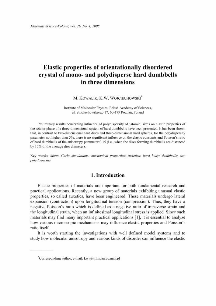
Materials Science-Poland, Vol. 26, No. 4, 2008
Elastic properties of orientationally disordered crystal of mono- and polydisperse hard dumbbells
in three dimensions
M. KOWALIK, K.W. WOJCIECHOWSKI*
Institute of Molecular Physics, Polish Academy of Sciences, ul. Smoluchowskiego 17, 60-179 Poznań, Poland
Preliminary results concerning influence of polydispersity of ‘atomic’ sizes on elastic properties of the rotator phase of a three-dimensional system of hard dumbbells have been presented. It has been shown that, in contrast to two-dimensional hard discs and three-dimensional hard spheres, for the polydispersity parameter not higher than 5%, there is no significant influence on the elastic constants and Poisson’s ratio of hard dumbbells of the anisotropy parameter 0.15 (i.e., when the discs forming dumbbells are distanced by 15% of the average disc diameter).
Key words: Monte Carlo simulations; mechanical properties; auxetics; hard body; dumbbells; size polydispersity
1. Introduction
Elastic properties of materials are important for both fundamental research and practical applications. Recently, a new group of materials exhibiting unusual elastic properties, so called auxetics, have been engineered. These materials undergo lateral expansion (contraction) upon longitudinal tension (compression). Thus, they have a negative Poisson’s ratio which is defined as a negative ratio of transverse strain and the longitudinal strain, when an infinitesimal longitudinal stress is applied. Since such materials may find many important practical applications [1], it is essential to analyze how various microscopic mechanisms may influence elastic properties and Poisson’s ratio itself.
It is worth starting the investigations with well defined model systems and to study how molecular anisotropy and various kinds of disorder can influence the elastic
__________
*Corresponding author, e-mail: [email protected]
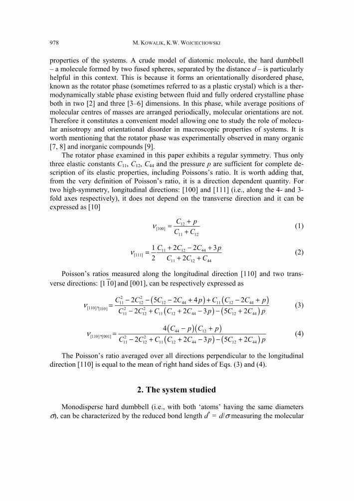
M. KOWALIK, K.W. WOJCIECHOWSKI 978
properties of the systems. A crude model of diatomic molecule, the hard dumbbell – a molecule formed by two fused spheres, separated by the distance d – is particularly helpful in this context. This is because it forms an orientationally disordered phase, known as the rotator phase (sometimes referred to as a plastic crystal) which is a ther-modynamically stable phase existing between fluid and fully ordered crystalline phase both in two [2] and three [3–6] dimensions. In this phase, while average positions of molecular centres of masses are arranged periodically, molecular orientations are not. Therefore it constitutes a convenient model allowing one to study the role of molecu-lar anisotropy and orientational disorder in macroscopic properties of systems. It is worth mentioning that the rotator phase was experimentally observed in many organic [7, 8] and inorganic compounds [9].
The rotator phase examined in this paper exhibits a regular symmetry. Thus only three elastic constants C11, C12, C44 and the pressure p are sufficient for complete de-scription of its elastic properties, including Poissons’s ratio. It is worth adding that, from the very definition of Poisson’s ratio, it is a direction dependent quantity. For two high-symmetry, longitudinal directions: [100] and [111] (i.e., along the 4- and 3-fold axes respectively), it does not depend on the transverse direction and it can be expressed as [10]
12[100]
11 12
C pC C
ν +=+
(1)
11 12 44[111]
11 12 44
1 2 2 32 2
C C C pC C C
ν + − +=+ +
(2)
Poisson’s ratios measured along the longitudinal direction [110] and two trans-verse directions: [1 10] and [001], can be respectively expressed as
( ) ( )( ) ( )
2 211 12 12 44 11 12 44
[110] 2 2[110]11 12 11 12 44 12 44
2 5 2 4 2,
2 2 3 5 2C C C C p C C C pC C C C C p C C p
ν− − − + + − +
=− + + − − +
(3)
( )( )( ) ( )
44 12[110] [001] 2 2
11 12 11 12 44 12 44
4,
2 2 3 5 2C p C p
C C C C C p C C pν
− +=
− + + − − + (4)
The Poisson’s ratio averaged over all directions perpendicular to the longitudinal direction [110] is equal to the mean of right hand sides of Eqs. (3) and (4).
2. The system studied
Monodisperse hard dumbbell (i.e., with both ‘atoms’ having the same diameters σ), can be characterized by the reduced bond length d* = d/σ measuring the molecular
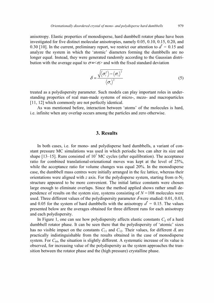
Orientationally disordered crystal of mono- and polydisperse hard dumbbells 979
anisotropy. Elastic properties of monodisperse, hard dumbbell rotator phase have been investigated for five distinct molecular anisotropies, namely 0.05, 0.10, 0.15, 0.20, and 0.30 [10]. In the current, preliminary report, we restrict our attention to d* = 0.15 and analyze the system in which the ‘atomic’ diameters forming the dumbbells are no longer equal. Instead, they were generated randomly according to the Gaussian distri-bution with the average equal to σ ≡<σi> and with the fixed standard deviation
22
2
i i
i
σ σδ
σ
−= (5)
treated as a polydispersity parameter. Such models can play important roles in under-standing properties of real man-made systems of micro-, mezo- and macroparticles [11, 12] which commonly are not perfectly identical.
As was mentioned before, interaction between ‘atoms’ of the molecules is hard, i.e. infinite when any overlap occurs among the particles and zero otherwise.
3. Results
In both cases, i.e. for mono- and polydisperse hard dumbbells, a variant of con-stant pressure MC simulations was used in which periodic box can alter its size and shape [13–15]. Runs consisted of 107 MC cycles (after equilibration). The acceptance ratio for combined translational-orienational moves was kept at the level of 25%, while the acceptance ratio for volume changes was equal 20%. In the monodisperse case, the dumbbell mass centres were initially arranged in the fcc lattice, whereas their orientations were aligned with z axis. For the polydisperse system, starting from α-N2 structure appeared to be more convenient. The initial lattice constants were chosen large enough to eliminate overlaps. Since the method applied shows rather small de-pendence of results on the system size, systems consisting of N =108 molecules were used. Three different values of the polydispersity parameter δ were studied: 0.01, 0.03, and 0.05 for the system of hard dumbbells with the anisotropy d* = 0.15. The values presented below are the averages obtained for three different runs for each anisotropy and each polydispersity.
In Figure 1, one can see how polydispersity affects elastic constants Cij of a hard dumbbell rotator phase. It can be seen there that the polydispersity of ‘atomic’ sizes has no visible impact on the constants C11 and C12. Their values, for different δ, are practically indistinguishable from the results obtained in the case of monodisperse system. For C44, the situation is slightly different. A systematic increase of its value is observed, for increasing value of the polydispersity as the system approaches the tran-sition between the rotator phase and the (high pressure) crystalline phase.
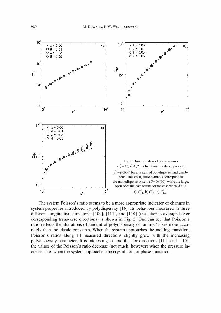
M. KOWALIK, K.W. WOJCIECHOWSKI 980
Fig. 1. Dimensionless elastic constants * 3 /ij ij BC C k Tσ= in function of reduced pressure
p* = pσ/kBT for a system of polydisperse hard dumb-bells. The small, filled symbols correspond to
the monodisperse system (δ = 0) [10], while the large, open ones indicate results for the case when δ > 0:
a) * * *11 12 44, b) , c) C C C
The system Poisson’s ratio seems to be a more appropriate indicator of changes in system properties introduced by polydispersity [16]. Its behaviour measured in three different longitudinal directions: [100], [111], and [110] (the latter is averaged over corresponding transverse directions) is shown in Fig. 2. One can see that Poisson’s ratio reflects the alterations of amount of polydispersity of ‘atomic’ sizes more accu-rately than the elastic constants. When the system approaches the melting transition, Poisson’s ratios along all measured directions slightly grow with the increasing polydispersity parameter. It is interesting to note that for directions [111] and [110], the values of the Poisson’s ratio decrease (not much, however) when the pressure in-creases, i.e. when the system approaches the crystal–rotator phase transition.
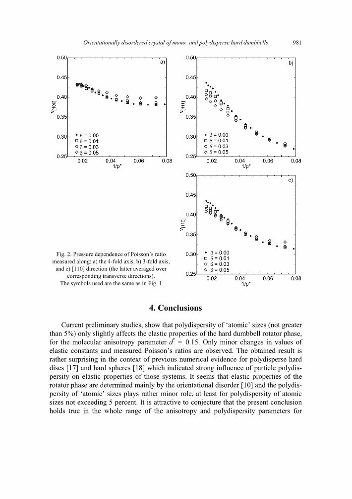
Orientationally disordered crystal of mono- and polydisperse hard dumbbells 981
Fig. 2. Pressure dependence of Poisson’s ratio measured along: a) the 4-fold axis, b) 3-fold axis,
and c) [110] direction (the latter averaged over corresponding transverse directions).
The symbols used are the same as in Fig. 1
4. Conclusions
Current preliminary studies, show that polydispersity of ‘atomic’ sizes (not greater than 5%) only slightly affects the elastic properties of the hard dumbbell rotator phase, for the molecular anisotropy parameter d* = 0.15. Only minor changes in values of elastic constants and measured Poisson’s ratios are observed. The obtained result is rather surprising in the context of previous numerical evidence for polydisperse hard discs [17] and hard spheres [18] which indicated strong influence of particle polydis-persity on elastic properties of those systems. It seems that elastic properties of the rotator phase are determined mainly by the orientational disorder [10] and the polydis-persity of ‘atomic’ sizes plays rather minor role, at least for polydispersity of atomic sizes not exceeding 5 percent. It is attractive to conjecture that the present conclusion holds true in the whole range of the anisotropy and polydispersity parameters for
M. KOWALIK, K.W. WOJCIECHOWSKI 982
which the rotator phase of hard dumbbells is stable. Work on this question is in pro-gress.
Acknowledgements
This work was supported by the Polish Office for Science and Higher Education, grant No. N20207032/1512 (2007-2010).
References
[1] WOJCIECHOWSKI K.W., ALDERSON A., ALDERSON K.L., MARUSZEWSKI B., SCARPA F., Phys. Stat. Sol. (b), 244 (2007), 813. See also other papers in that issue.
[2] WOJCIECHOWSKI K.W., Phys. Lett. A, 137 (1986), 60. [3] SINGER S.J., MUMAUGH R., J. Chem. Phys., 93 (1990), 1278. [4] VEGA C., PARAS E.P.A., MONSON P.A., J. Chem. Phys., 96 (1992), 9060. [5] VEGA C., PARAS E.P.A., MONSON P.A., J. Chem. Phys., 97 (1992), 8543. [6] VEGA C., MONSON P.A., J. Chem. Phys., 107 (1992), 8543. [7] CABRILLO C., BERMEJO F.J., JIMÉNEZ-RUIZ M., FERNÁNDEZ-DÍAZ M.T., GONZALEZ M.A., MARTÍN Y.,
MARERO D., Phys. Rev. B, 64 (2001), 064206. [8] SHINOHARA Y., KAWASAKI N., UENO S., KOBAYASHI I., NAKAJIMA M., AMEMIYA Y., Phys. Rev. Lett.,
94 (2005), 097801. [9] TÄRNEBERG R., LUNDEN A., Solid State Ionics, 90 (1996), 209.
[10] KOWALIK M., WOJCIECHOWSKI K.W., J. Non-Cryst. Solids, 352 (2006), 4269. [11] VON BLAADEREN A., MRS Bull., 29 (2004), 85. [12] MANOHARAN V.N., PINE D.J., MRS Bull., 29 (2004), 91. [13] WOJCIECHOWSKI K.W., TRETIAKOV K.V., Comput. Phys. Commun., 121–122 (1999), 528. [14] WOJCIECHOWSKI K.W., Comput. Methods Sci. Technol., 8 (2002), 73. [15] WOJCIECHOWSKI K.W., TRETIAKOV K.V., KOWALIK M., Phys. Rev. E, 67 (2003), 036121. [16] TRETIAKOV K.V., WOJCIECHOWSKI K.W., J. Phys. Condens. Matter, 14 (2003), 1261-1273. [17] TRETIAKOV K.V., WOJCIECHOWSKI K.W., unpublished. [18] NAROJCZYK J.W., WOJCIECHOWSKI K.W., Mater. Sci.-Poland, 26 (2008), 995.
Received 7 May 2007 Revised 22 September 2007
Materials Science-Poland, Vol. 26, No. 4, 2008
Modelling of magnetization reversal for long ferromagnetic nanotubes
K. M. LEBECKI*
Institute of Physics, Polish Academy of Sciences, al. Lotników 32/46, 02-668 Warsaw, Poland
The theory of infinite tube magnetization reversal, formulated by Lee and Chang, has been reconsid-ered. For this purpose, a standard micromagnetic simulation package OOMMF was used. To account for elongated geometry of ferromagnetic nanotubes grown nowadays, an extension module has been written allowing application of periodic boundary conditions in one dimension. The results of the modelling exhibit a basic agreement with the theory. Limitations of the approach have been described and check-points have been discussed necessary in finite difference simulations performed for such structures.
Key words: magnetic nanowires; micromagnetic modelling; magnetization reversal; coercivity
1. Introduction
Self-assembly [1] as a cheap and reliable method to grow structured systems has been attracting interest for many years. Among samples intensively studied in recent years are ferromagnetic nanoobjects, due to their potential application in spintronic devices and interesting basic science phenomena. Such structures are often produced within porous matrix, and contain magnetic nanowires, see, e.g., review papers [2]. Beside nanowires, there are, however, already a few reports of successful growth of magnetic nanotubes, either hollow or filled with a semiconductor [3]. This situation opens a novel possibility to build hybrid ferromagnetic–semiconductor systems. When considering such structures, a question arises what are the magnetization properties of a long ferromagnetic tube itself. To answer this question we re-evaluate the theory of infinite tube magnetization and compare it with micromagnetic modelling. We high-light the necessary checkpoints that should be monitored during simulation of such structures. __________
*E-mail: lebecki ifpan.edu.pl
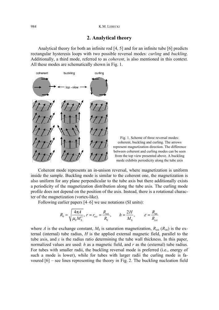
K.M. LEBECKI 984
2. Analytical theory
Analytical theory for both an infinite rod [4, 5] and for an infinite tube [6] predicts rectangular hysteresis loops with two possible reversal modes: curling and buckling. Additionally, a third mode, referred to as coherent, is also mentioned in this context. All these modes are schematically shown in Fig. 1.
Fig. 1. Scheme of three reversal modes: coherent, buckling and curling. The arrows
represent magnetization direction. The difference between coherent and curling modes can be seen from the top view presented above. A buckling mode exhibits periodicity along the tube axis
Coherent mode represents an in-unison reversal, where magnetization is uniform inside the sample. Buckling mode is similar to the coherent one, the magnetization is also uniform for any plane perpendicular to the tube axis but there additionally exists a periodicity of the magnetization distribution along the tube axis. The curling mode profile does not depend on the position of the axis. Instead, there is a rotational charac-ter of the magnetization (vortex-like).
Following earlier papers [4–6] we use notations (SI units):
0 20 S
4π ,ARMμ
= extext
0
,Rr rR
= =S
2 ,HhM
= int
ext
RR
ε =
where A is the exchange constant, MS is saturation magnetization, Rext (Rint) is the ex-ternal (internal) tube radius, H is the applied external magnetic field, parallel to the tube axis, and ε is the radius ratio determining the tube wall thickness. In this paper, normalized values are used: h as a magnetic field, and r as the (external) tube radius. For tubes with smaller radii, the buckling reversal mode is preferred (i.e., energy of such a mode is lower), while for tubes with larger radii the curling mode is fa-voured [6] – see lines representing the theory in Fig. 2. The buckling nucleation field
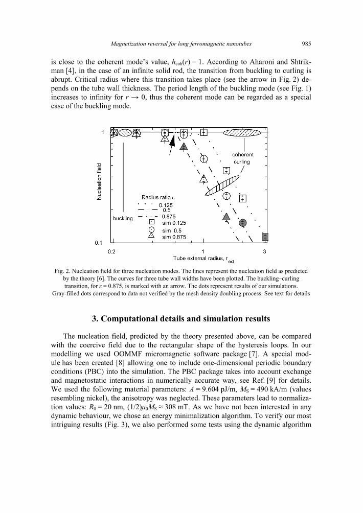
Magnetization reversal for long ferromagnetic nanotubes 985
is close to the coherent mode’s value, hcoh(r) = 1. According to Aharoni and Shtrik-man [4], in the case of an infinite solid rod, the transition from buckling to curling is abrupt. Critical radius where this transition takes place (see the arrow in Fig. 2) de-pends on the tube wall thickness. The period length of the buckling mode (see Fig. 1) increases to infinity for r → 0, thus the coherent mode can be regarded as a special case of the buckling mode.
Fig. 2. Nucleation field for three nucleation modes. The lines represent the nucleation field as predicted by the theory [6]. The curves for three tube wall widths have been plotted. The buckling–curling transition, for ε = 0.875, is marked with an arrow. The dots represent results of our simulations.
Gray-filled dots correspond to data not verified by the mesh density doubling process. See text for details
3. Computational details and simulation results
The nucleation field, predicted by the theory presented above, can be compared with the coercive field due to the rectangular shape of the hysteresis loops. In our modelling we used OOMMF micromagnetic software package [7]. A special mod-ule has been created [8] allowing one to include one-dimensional periodic boundary conditions (PBC) into the simulation. The PBC package takes into account exchange and magnetostatic interactions in numerically accurate way, see Ref. [9] for details. We used the following material parameters: A = 9.604 pJ/m, MS = 490 kA/m (values resembling nickel), the anisotropy was neglected. These parameters lead to normaliza-tion values: R0 = 20 nm, (1/2)μ0MS ≈ 308 mT. As we have not been interested in any dynamic behaviour, we chose an energy minimalization algorithm. To verify our most intriguing results (Fig. 3), we also performed some tests using the dynamic algorithm
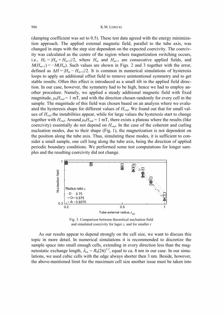
K.M. LEBECKI 986
(damping coefficient was set to 0.5). These test data agreed with the energy minimiza-tion approach. The applied external magnetic field, parallel to the tube axis, was changed in steps with the step size dependent on the expected coercivity. The coerciv-ity was calculated as the centre of the region where magnetization switching occurs, i.e., HC = |Hm + Hm+1|/2, where Hm and Hm+1 are consecutive applied fields, and M(Hm+1) = −M(Hm). Such values are shown in Figs. 2 and 3 together with the error, defined as ΔH = |Hm − Hm+1|/2. It is common in numerical simulations of hysteresis loops to apply an additional offset field to remove unintentional symmetry and to get stable results. Often this effect is introduced as a small tilt in the applied field direc-tion. In our case, however, the symmetry had to be high, hence we had to employ an-other procedure. Namely, we applied a steady additional magnetic field with fixed magnitude, μ0Hrnd = 1 mT, and with the direction chosen randomly for every cell in the sample. The magnitude of this field was chosen based on an analysis where we evalu-ated the hysteresis shape for different values of Hrnd. We found out that for small val-ues of Hrnd the instabilities appear, while for large values the hysteresis start to change together with Hrnd. Around μ0Hrnd = 1 mT, there exists a plateau where the results (like coercivity) essentially do not depend on Hrnd. In the case of the coherent and curling nucleation modes, due to their shape (Fig. 1), the magnetization is not dependent on the position along the tube axis. Thus, simulating these modes, it is sufficient to con-sider a small sample, one cell long along the tube axis, being the direction of applied periodic boundary conditions. We performed some test computations for longer sam-ples and the resulting coercivity did not change.
Fig. 3. Comparison between theoretical nucleation field and simulated coercivity for lager ε, and for smaller r
As our results appear to depend strongly on the cell size, we want to discuss this topic in more detail. In numerical simulations it is recommended to discretize the sample space into small enough cells, extending in every direction less than the mag-netostatic exchange length, λex = R0(2π)1/2, equal to ca. 8 nm in our case. In our simu-lations, we used cubic cells with the edge always shorter then 3 nm. Beside, however, the above-mentioned limit for the maximum cell size another issue must be taken into
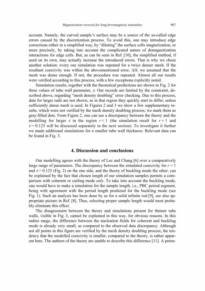
Magnetization reversal for long ferromagnetic nanotubes 987
account. Namely, the curved sample’s surface may be a source of the so-called edge errors caused by the discretization process. To avoid this, one may introduce edge corrections either in a simplified way, by “diluting” the surface cells magnetization, or more precisely, by taking into account the complicated nature of demagnetization interactions for edge cells. But, as can be seen in Ref. [10], the simplified method, if used on its own, may actually increase the introduced errors. That is why we chose another solution: every our simulation was repeated for a twice denser mesh. If the resultant coercivity was within the abovementioned error, ΔH, we assumed that the mesh was dense enough. If not, the procedure was repeated. Almost all our results were verified according to this process, with a few exceptions explicitly noted.
Simulation results, together with the theoretical predictions are shown in Fig. 2 for three values of tube wall parameter, ε. Our records are limited by the constraint, de-scribed above, regarding “mesh density doubling” error checking. Due to this process, data for larger radii are not shown, as in that region they quickly start to differ, unless sufficiently dense mesh is used. In Figures 2 and 3 we show a few supplementary re-sults, which were not verified by the mesh density doubling process; we mark them as gray-filled dots. From Figure 2, one can see a discrepancy between the theory and the modelling for larger ε in the region r < 1 (the simulation result for r = 1 and ε = 0.125 will be discussed separately in the next section). To investigate it further we made additional simulations for a smaller tube wall thickness. Relevant data can be found in Fig. 3.
4. Discussion and conclusions
Our modelling agrees with the theory of Lee and Chang [6] over a comparatively large range of parameters. The discrepancy between the simulated coercivity for r = 1 and ε = 0.125 (Fig. 2) on the one side, and the theory of buckling mode the other, can be explained by the fact that chosen length of our simulation samples permits a com-parison with coherent or curling mode only. To take into account the buckling mode, one would have to make a simulation for the sample length, i.e., PBC period segment, being with agreement with the period length predicted for the buckling mode (see Fig. 1). Such an analysis has been done by us for a solid infinite rod [9], see also ap-propriate picture in Ref. [8]. Thus, selecting proper sample length would most proba-bly eliminate this effect.
The disagreement between the theory and simulations present for thinner tube walls, visible in Fig. 3, cannot be explained in this way, for obvious reasons. In this radius range, the difference between the nucleation fields for coherent and buckling mode is already very small, as compared to the observed data discrepancy. Although not all points in this figure are verified by the mesh density doubling process, the ten-dency that the modelled coercivity is smaller, compared to the theory, is rather appar-ent here. The authors of the theory are unable to describe this difference [11]. A poten-
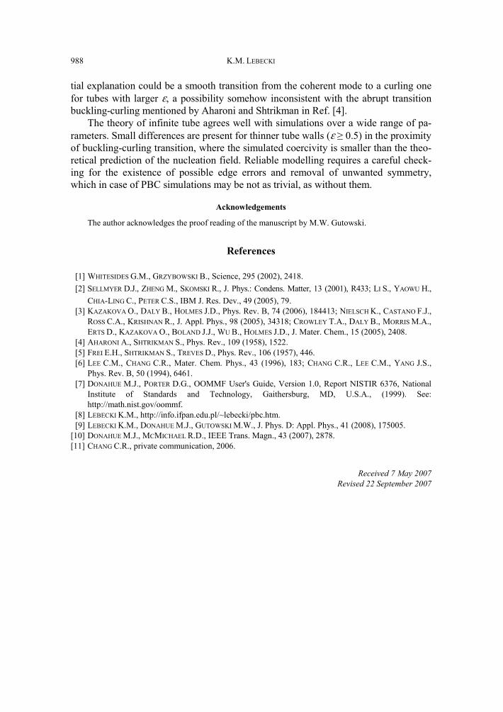
K.M. LEBECKI 988
tial explanation could be a smooth transition from the coherent mode to a curling one for tubes with larger ε, a possibility somehow inconsistent with the abrupt transition buckling-curling mentioned by Aharoni and Shtrikman in Ref. [4].
The theory of infinite tube agrees well with simulations over a wide range of pa-rameters. Small differences are present for thinner tube walls (ε ≥ 0.5) in the proximity of buckling-curling transition, where the simulated coercivity is smaller than the theo-retical prediction of the nucleation field. Reliable modelling requires a careful check-ing for the existence of possible edge errors and removal of unwanted symmetry, which in case of PBC simulations may be not as trivial, as without them.
Acknowledgements
The author acknowledges the proof reading of the manuscript by M.W. Gutowski.
References
[1] WHITESIDES G.M., GRZYBOWSKI B., Science, 295 (2002), 2418. [2] SELLMYER D.J., ZHENG M., SKOMSKI R., J. Phys.: Condens. Matter, 13 (2001), R433; LI S., YAOWU H.,
CHIA-LING C., PETER C.S., IBM J. Res. Dev., 49 (2005), 79. [3] KAZAKOVA O., DALY B., HOLMES J.D., Phys. Rev. B, 74 (2006), 184413; NIELSCH K., CASTANO F.J.,
ROSS C.A., KRISHNAN R., J. Appl. Phys., 98 (2005), 34318; CROWLEY T.A., DALY B., MORRIS M.A., ERTS D., KAZAKOVA O., BOLAND J.J., WU B., HOLMES J.D., J. Mater. Chem., 15 (2005), 2408.
[4] AHARONI A., SHTRIKMAN S., Phys. Rev., 109 (1958), 1522. [5] FREI E.H., SHTRIKMAN S., TREVES D., Phys. Rev., 106 (1957), 446. [6] LEE C.M., CHANG C.R., Mater. Chem. Phys., 43 (1996), 183; CHANG C.R., LEE C.M., YANG J.S.,
Phys. Rev. B, 50 (1994), 6461. [7] DONAHUE M.J., PORTER D.G., OOMMF User's Guide, Version 1.0, Report NISTIR 6376, National
Institute of Standards and Technology, Gaithersburg, MD, U.S.A., (1999). See: http://math.nist.gov/oommf.
[8] LEBECKI K.M., http://info.ifpan.edu.pl/~lebecki/pbc.htm. [9] LEBECKI K.M., DONAHUE M.J., GUTOWSKI M.W., J. Phys. D: Appl. Phys., 41 (2008), 175005.
[10] DONAHUE M.J., MCMICHAEL R.D., IEEE Trans. Magn., 43 (2007), 2878. [11] CHANG C.R., private communication, 2006.
Received 7 May 2007 Revised 22 September 2007
Materials Science-Poland, Vol. 26, No. 4, 2008
Spin-wave theory of spin-polarized electron energy loss spectroscopy (SPEELS) measurements
in 5 ML Fe film deposited on W(110)
S. MAMICA*, H. PUSZKARSKI Surface Physics Division, Institute of Physics, Adam Mickiewicz University,
ul. Umułtowska 85, 61-614 Poznań, Poland
Detection of spin waves with higher wave vector values is now possible with spin-polarized electron energy loss spectroscopy (SPEELS), a method recently reported to have been applied for detecting spin waves in a range of wave vector values covering in principle the whole Brillouin zone. This paper pre-sents a comparison of spin-wave spectra resulting from our theoretical investigations (within the model based on a bilinear Hamiltonian expressed in second-quantization formalism) with the corresponding SPEELS results obtained recently for 5 ML Fe film deposited on W(110). By considering the mixed bcc-fcc film structure we were able to explain details of the reported SPEELS spectra, indicating the surface character of the modes associated with the observed peaks.
Key words: spin waves; SPEELS; ultrathin Fe film
1. Introduction
Due to the recent dynamic development of magnetoelectronics, properties of spin waves in magnetic thin film systems have been intensively studied both experimentally and theoretically. The standard experimental methods of probing spin waves, i.e. ferro-magnetic resonance (FMR) and Brillouin light scattering (BLS), only allow investigation of waves with low wave vector values (wave vector near the Brillouin zone centre). This limitation does not apply to spin-polarized electron energy loss spectroscopy (SPEELS) [1–4]. Besides allowing penetration of the whole Brillouin zone, SPEELS has an advan-tage of being especially sensitive to surface spin waves. Recent studies by Vollmer et al. on Co and Fe ultra-thin films [5, 6] are of particular interest in this context.
The paper presents the results of our calculations of ultra thin film spin wave en-ergy spectra, providing a basis for a tentative interpretation of the SPEELS spectrum obtained for 5 ML Fe/W(110) and reported in [6].
__________
*Corresponding author, e-mail: [email protected]
S. MAMICA, H. PUSZKARSKI
990
2. Essentials of SPEELS experiment on 5 ML Fe deposited on W(110)
The inelastic electron scattering occurring in a SPEELS experiment results in en-ergy and momentum transfer from the scattered electrons to the studied sample. The incident electron beam is spin-polarized, the polarization being either antiparallel (↑) or parallel (↓) to the magnetization of the sample. The scattering itself can occur in two ways: either an incident electron is reflected, passing a part of its energy and mo-mentum to electrons in the sample, or it knocks out an electron of the sample to take its place. In the latter case, if the spin of the incident electron is antiparallel to the magnetization of the sample, the magnetization will decrease by g μB, producing a spin excitation (such as a Stoner excitation or a spin wave). The electron knocked out of the sample will join the scattered beam, resulting in its spin polarization asym-metry. The essence of SPEELS is the measurement of the scattered intensity as a func-tion of two parameters: the energy loss (Eloss) and the wave vector component parallel to the surface (kII). The asymmetry spectrum measured in function of Eloss and kII con-tains information on spin excitations that have occurred in the scattering process. On the other hand, as the scattered electrons are monochromatic and of low energy (in the order of 10 eV), their penetration range into the sample is as low as a few atomic lay-ers; therefore, the information obtained principally concerns the surface region of the studied sample.
The SPEEL measurements reported in [6] were performed on an ultrathin (5 ML) Fe layer set on a W(110) substrate by the molecular beam epitaxy (MBE) at room temperature. Upon preparation, the sample was magnetized in-plane along the easy-magnetization direction (<110> in Fe/W(110) thin films). The chosen electron scatter-ing plane was perpendicular to the magnetization direction. The resulting SPEEL in-tensity spectrum, as well as the asymmetry spectra corresponding to four wave vector values (kII = –0.17 Å–1, –0.35 Å–1, –0.69 Å–1 and –1.03 Å–1) are shown in [6], Fig. 5. Two regions can be distinguished in the asymmetry spectrum: above 500 meV, with asymmetry characteristic of Stoner excitations, and below 500 meV, with a very wide line extending from about 100 meV to 500 meV and showing two clearly separated peaks at 215 meV and 310 meV. The spectrum shows no significant dispersion, as the positions of the peaks remain the same in all four spectra obtained for the four differ-ent wave vector values. On the other hand, SPEEL asymmetry increases with the wave vector value (from ca. 0.1 for kII = –0.17 Å–1 to ca. 0.2 for kII = –1.03 Å–1). The ob-tained wide line is attributed by the authors to a spin wave excitation, and the notch separating the two peaks is associated with vibration losses due to adsorption species deposited on the sample surface during measurements (which is of importance because of long measurement time).
Key information necessary for proper interpretation of the spectrum obtained is that about the structure of the studied sample. The structure of ultrathin Fe layers was studied, among others, in [7], reporting the results of STM investigation of Fe films of
Spin-wave theory of spin-polarized electron energy loss spectroscopy
991
the thickness ranging from 1 ML to 5 ML, set on a Cu(001) substrate by the MBE method. In contrast to the ‘bulk’ Fe, which shows the α (bcc) structure at temperatures below 1185 K, thin-film Fe (of thickness up to 4 ML) has the fcc structure. The thick-ness threshold, above which reconstruction to the bcc structure occurs, is approxi-mately 4–5 ML. Therefore, ultra-thin Fe layers of the thickness close to the threshold value are assumed to have a mixed structure [7] with alternating bcc and fcc phases, and the SPEEL spectrum discussed above can be expected to contain information on spin waves occurring concurrently in both structure types. Assuming this point of view, we think the two peaks in the asymmetry spectrum can be associated with exci-tation of two different spin waves, and the observed asymmetry increase with the wave vector value might suggest their surface character. A theoretical elaboration of this idea is presented below.
3. Theoretical results
In order to verify our hypothesis, we have calculated the energy spectra of spin waves in a thin film of mixed bcc–fcc structure and surface cut (110). The calculations were performed within the framework of the Heisenberg localized spin model, assum-ing an exchange (nearest neighbour only) and Zeeman Hamiltonian in the standard form:
( )
eff
;
ˆ ˆ ˆ2 l l ll l l
H J gμ′ ′′ ′
= − ⋅ − ⋅∑ ∑j j jj j j
S S H S (1)
Heff comprising both external and demagnetizing fields. The sums extend over differ-ent pairs of neighbouring spins, lj defining the spin position; l is the layer number and j denotes the two-dimensional vector defining the position of the spin in the l-th layer. We diagonalize the Hamiltonian (1) by applying the procedure described in [8].
Figure 1 shows the numerically determined energy spectra of spin waves in a thin film of thickness L = 5 ML and exchange constant 2SJ = 36 meV. The spectra corre-sponding to the fcc and the bcc structures are shown in Figs. 1a, b, respectively. Both spectra were calculated for surface cut (110), along the characteristic path in the re-spective 2D Brillouin zone (see the inset in each plot). The solid lines represent the energy of individual modes, and the shaded area denotes the hypothetical band region. In both the fcc(110) and the bcc(110) structures the Brilloun zone features regions in which the two lowest modes are of surface nature (see Fig. 1c). In the fcc(110) struc-ture, the second surface mode appears between points Δ and X to vanish between Y and Σ; in the bcc(110) structure, the second surface mode appears in the vicinity of point C to vanish around point Σ. Indicated in Figure 1, the lowest surface mode en-ergy values are 310 meV and 216 meV in the fcc(110) and bcc(110) structures, respec-tively. These values exactly correspond to the position of the peaks in the SPEEL asymmetry spectra obtained in the above-discussed experiment. Note also that in both
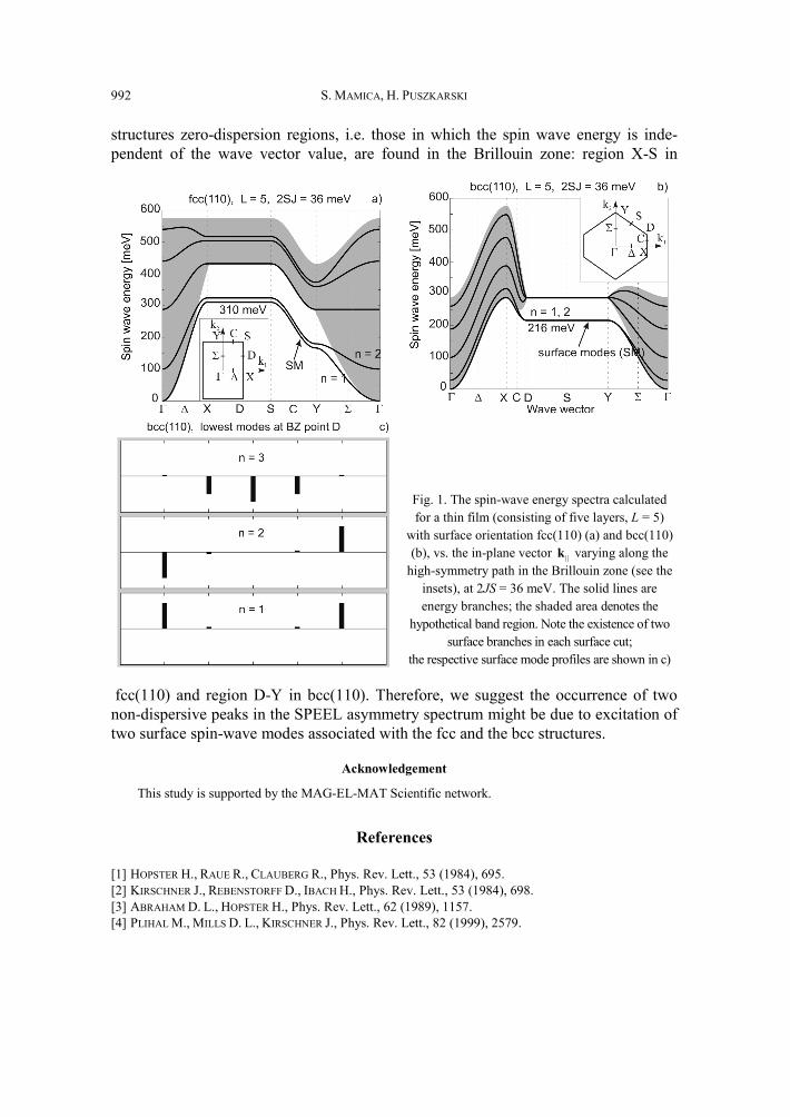
S. MAMICA, H. PUSZKARSKI
992
structures zero-dispersion regions, i.e. those in which the spin wave energy is inde-pendent of the wave vector value, are found in the Brillouin zone: region X-S in
Fig. 1. The spin-wave energy spectra calculated for a thin film (consisting of five layers, L = 5)
with surface orientation fcc(110) (a) and bcc(110) (b), vs. the in-plane vector ||k varying along the
high-symmetry path in the Brillouin zone (see the insets), at 2JS = 36 meV. The solid lines are energy branches; the shaded area denotes the
hypothetical band region. Note the existence of two surface branches in each surface cut;
the respective surface mode profiles are shown in c)
fcc(110) and region D-Y in bcc(110). Therefore, we suggest the occurrence of two non-dispersive peaks in the SPEEL asymmetry spectrum might be due to excitation of two surface spin-wave modes associated with the fcc and the bcc structures.
Acknowledgement
This study is supported by the MAG-EL-MAT Scientific network.
References
[1] HOPSTER H., RAUE R., CLAUBERG R., Phys. Rev. Lett., 53 (1984), 695. [2] KIRSCHNER J., REBENSTORFF D., IBACH H., Phys. Rev. Lett., 53 (1984), 698. [3] ABRAHAM D. L., HOPSTER H., Phys. Rev. Lett., 62 (1989), 1157. [4] PLIHAL M., MILLS D. L., KIRSCHNER J., Phys. Rev. Lett., 82 (1999), 2579.

Spin-wave theory of spin-polarized electron energy loss spectroscopy
993
[5] VOLLMER R., ETZKORN M., ANIL KUMAR P. S., IBACH H., KIRSCHNER J., Phys. Rev. Lett., 91 (2003), 147201.
[6] VOLLMER R., ETZKORN M., ANIL KUMAR P. S., IBACH H., KIRSCHNER J., J. Magn. Magn. Mater., 272–276 (2004), 2126.
[7] BIEDERMANN A., TSCHELIESSNIG R., SCHMID M., VARGA P., Phys. Rev. Lett., 87 (2001), 086103. [8] MAMICA S., PUSZKARSKI H., The effect of crystallographic surface cut on surface state existence con-
ditions in cubic thin films. Application to magnetic films, [in:] A. Ghazali, J.-C.S. Lévy (Eds.), Surface Magnetism and Nanostructure, Research Singpost, Kerala, 2006, p. 129.
Received 7 May 2007 Revised 22 September 2007
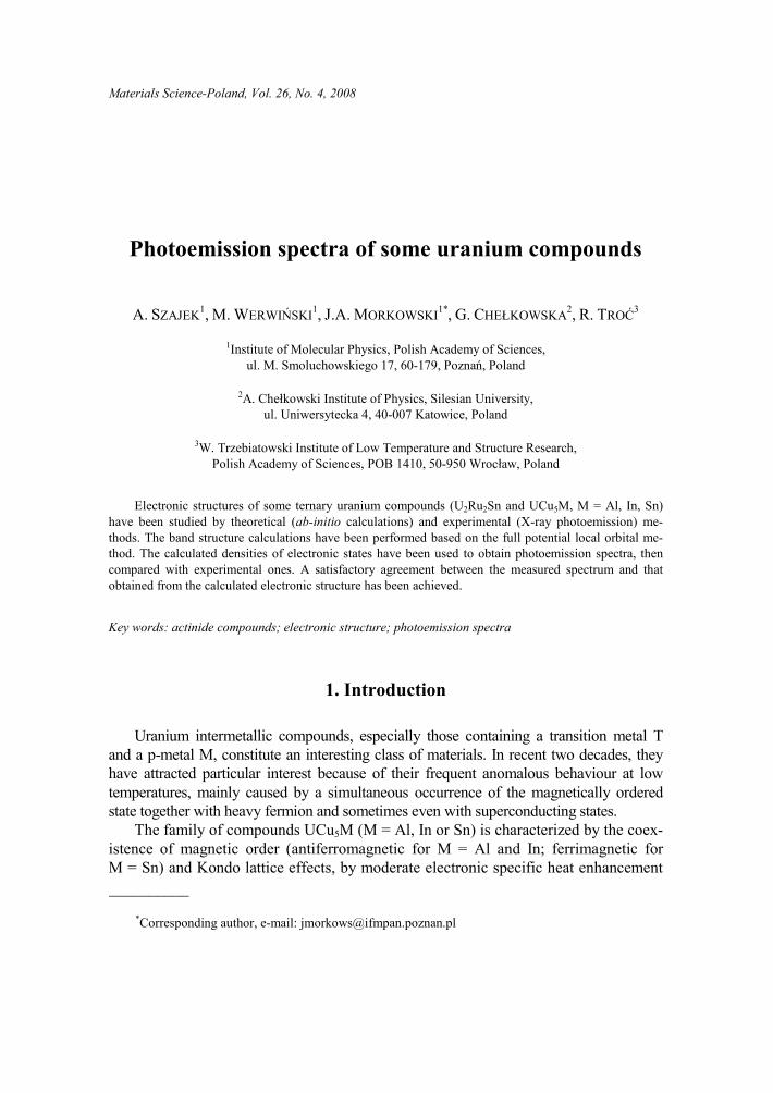
Materials Science-Poland, Vol. 26, No. 4, 2008
Photoemission spectra of some uranium compounds
A. SZAJEK1, M. WERWIŃSKI1, J.A. MORKOWSKI1*, G. CHEŁKOWSKA2, R. TROĆ3
1Institute of Molecular Physics, Polish Academy of Sciences, ul. M. Smoluchowskiego 17, 60-179, Poznań, Poland
2A. Chełkowski Institute of Physics, Silesian University, ul. Uniwersytecka 4, 40-007 Katowice, Poland
3W. Trzebiatowski Institute of Low Temperature and Structure Research, Polish Academy of Sciences, POB 1410, 50-950 Wrocław, Poland
Electronic structures of some ternary uranium compounds (U2Ru2Sn and UCu5M, M = Al, In, Sn) have been studied by theoretical (ab-initio calculations) and experimental (X-ray photoemission) me-thods. The band structure calculations have been performed based on the full potential local orbital me-thod. The calculated densities of electronic states have been used to obtain photoemission spectra, then compared with experimental ones. A satisfactory agreement between the measured spectrum and that obtained from the calculated electronic structure has been achieved.
Key words: actinide compounds; electronic structure; photoemission spectra
1. Introduction
Uranium intermetallic compounds, especially those containing a transition metal T and a p-metal M, constitute an interesting class of materials. In recent two decades, they have attracted particular interest because of their frequent anomalous behaviour at low temperatures, mainly caused by a simultaneous occurrence of the magnetically ordered state together with heavy fermion and sometimes even with superconducting states.
The family of compounds UCu5M (M = Al, In or Sn) is characterized by the coex-istence of magnetic order (antiferromagnetic for M = Al and In; ferrimagnetic for M = Sn) and Kondo lattice effects, by moderate electronic specific heat enhancement __________
*Corresponding author, e-mail: [email protected]
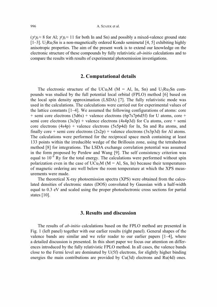
A. SZAJEK et al. 996
(γ/γ0 ≈ 8 for Al; γ/γ0 ≈ 11 for both In and Sn) and possibly a mixed-valence ground state [1–3]. U2Ru2Sn is a non-magnetically ordered Kondo semimetal [4, 5] exhibiting highly anisotropic properties. The aim of the present work is to extend our knowledge on the electronic structure of these compounds by fully relativistic ab-initio calculations and to compare the results with results of experimental photoemission investigations.
2. Computational details
The electronic structure of the UCu5M (M = Al, In, Sn) and U2Ru2Sn com-pounds was studied by the full potential local orbital (FPLO) method [6] based on the local spin density approximation (LSDA) [7]. The fully relativistic mode was used in the calculations. The calculations were carried out for experimental values of the lattice constants [1–4]. We assumed the following configurations of atoms: core + semi core electrons (5d6s) + valence electrons (6p7s7p6d5f) for U atoms, core + semi core electrons (3s3p) + valence electrons (4s4p3d) for Cu atoms, core + semi core electrons (4s4p) + valence electrons (5s5p4d) for In, Sn and Ru atoms, and finally core + semi core electrons (2s2p) + valence electrons (3s3p3d) for Al atoms. The calculations were performed for the reciprocal space mesh containing at least 133 points within the irreducible wedge of the Brillouin zone, using the tetrahedron method [8] for integrations. The LSDA exchange correlation potential was assumed in the form proposed by Perdew and Wang [9]. The self consistency criterion was equal to 10–8 Ry for the total energy. The calculations were performed without spin polarization even in the case of UCu5M (M = Al, Sn, In) because their temperatures of magnetic ordering are well below the room temperature at which the XPS meas-urements were made.
The theoretical X-ray photoemission spectra (XPS) were obtained from the calcu-lated densities of electronic states (DOS) convoluted by Gaussian with a half-width equal to 0.3 eV and scaled using the proper photoelectronic cross sections for partial states [10].
3. Results and discussion
The results of ab-initio calculations based on the FPLO method are presented in Fig. 1 (left panel) together with our earlier results (right panel). General shapes of the valence bands are similar and we refer reader to our earlier papers [1–4], where a detailed discussion is presented. In this short paper we focus our attention on differ-ences introduced by the fully relativistic FPLO method. In all cases, the valence bands close to the Fermi level are dominated by U(5f) electrons, for slightly higher binding energies the main contributions are provided by Cu(3d) electrons and Ru(4d) ones.
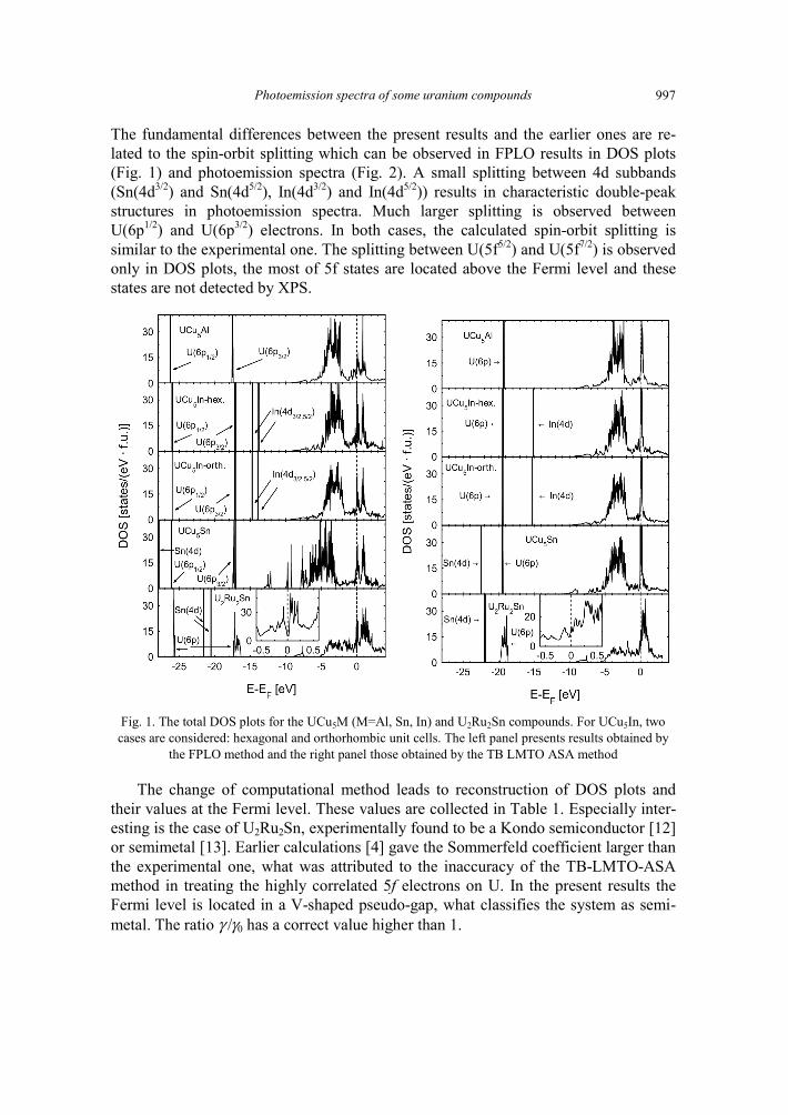
Photoemission spectra of some uranium compounds 997
The fundamental differences between the present results and the earlier ones are re-lated to the spin-orbit splitting which can be observed in FPLO results in DOS plots (Fig. 1) and photoemission spectra (Fig. 2). A small splitting between 4d subbands (Sn(4d3/2) and Sn(4d5/2), In(4d3/2) and In(4d5/2)) results in characteristic double-peak structures in photoemission spectra. Much larger splitting is observed between U(6p1/2) and U(6p3/2) electrons. In both cases, the calculated spin-orbit splitting is similar to the experimental one. The splitting between U(5f5/2) and U(5f7/2) is observed only in DOS plots, the most of 5f states are located above the Fermi level and these states are not detected by XPS.
Fig. 1. The total DOS plots for the UCu5M (M=Al, Sn, In) and U2Ru2Sn compounds. For UCu5In, two cases are considered: hexagonal and orthorhombic unit cells. The left panel presents results obtained by
the FPLO method and the right panel those obtained by the TB LMTO ASA method
The change of computational method leads to reconstruction of DOS plots and their values at the Fermi level. These values are collected in Table 1. Especially inter-esting is the case of U2Ru2Sn, experimentally found to be a Kondo semiconductor [12] or semimetal [13]. Earlier calculations [4] gave the Sommerfeld coefficient larger than the experimental one, what was attributed to the inaccuracy of the TB-LMTO-ASA method in treating the highly correlated 5f electrons on U. In the present results the Fermi level is located in a V-shaped pseudo-gap, what classifies the system as semi-metal. The ratio γ /γ0 has a correct value higher than 1.
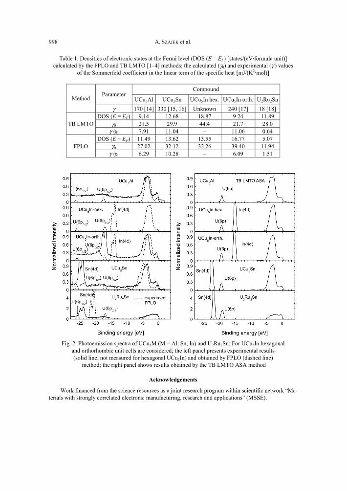
A. SZAJEK et al. 998
Table 1. Densities of electronic states at the Fermi level (DOS (E = EF) [states/(eV·formula unit)] calculated by the FPLO and TB LMTO [1–4] methods; the calculated (γ0) and experimental (γ ) values
of the Sommerfeld coefficient in the linear term of the specific heat [mJ/(K2·mol)]
Method Parameter
Compound
UCu5Al UCu5Sn UCu5In hex. UCu5In orth. U2Ru2Sn γ 170 [14] 330 [15, 16] Unknown 240 [17] 18 [18]
TB LMTO DOS (E = EF) 9.14 12.68 18.87 9.24 11.89
γ0 21.5 29.9 44.4 21.7 28.0 γ /γ0 7.91 11.04 – 11.06 0.64
FPLO DOS (E = EF) 11.49 13.62 13.55 16.77 5.07
γ0 27.02 32.12 32.26 39.40 11.94 γ /γ0 6.29 10.28 – 6.09 1.51
Fig. 2. Photoemission spectra of UCu5M (M = Al, Sn, In) and U2Ru2Sn; For UCu5In hexagonal
and orthorhombic unit cells are considered; the left panel presents experimental results (solid line; not measured for hexagonal UCu5In) and obtained by FPLO (dashed line)
method; the right panel shows results obtained by the TB LMTO ASA method
Acknowledgements
Work financed from the science resources as a joint research program within scientific network “Ma-terials with strongly correlated electrons: manufacturing, research and applications” (MSSE).
Photoemission spectra of some uranium compounds 999
References
[1] CHEŁKOWSKA G., MORKOWSKI J.A., SZAJEK A., TROĆ R., Phys. Rev. B, 64 (2001), 075119. [2] CHEŁKOWSKA G., MORKOWSKI J.A., SZAJEK A., TROĆ R., J. Phys.: Condens. Matter, 14 (2002), 3199. [3] CHEŁKOWSKA G., MORKOWSKI J.A., SZAJEK A., TROĆ R., Phil. Mag. B, 82 (2002), 1893. [4] CHEŁKOWSKA G., MORKOWSKI J.A., SZAJEK A., STĘPIEŃ-DAMM J., TROĆ R., European J. Phys. B, 35
(2003), 349. [5] STRYDOM A.M., TROĆ R., Solid State Commun. 126 (2003), 207. [6] KOEPERNIK K., ESCHRIG H., Phys. Rev. B, 59 (1999), 1743. [7] OPAHLE I., KOEPERNIK K., ESCHRIG H., Phys. Rev. B, 60 (1999), 14035. [8] BLÖCHL P., JEPSEN O., ANDERSEN O.K., Phys. Rev. B, 49 (1994), 16223. [9] PERDEW J.P., WANG Y., Phys. Rev. B, 45 (1992), 13244.
[10] YEH J.J., LINDAU I., At. Data Nucl. Data Tables, 32 (1985) 1. [11] ANDERSEN O.K., Phys. Rev. B, 12 (1975), 3060. [12] DU PLESSIS P. DE V., STRYDOM A.M., TROĆ R., MENON L., J. Phys.: Condens. Matter, 13 (2001),
8375. [13] PASCHEN S., BAENITZ M., TRAN V.H., RABIS A., STEGLICH F., CARRILO-CABRERA W., GRIN YU.,
STRYDOM A.M., DU PLESSIS P. DE V., J. Phys. Chem. Solids, 63 (2002), 1183. [14] TROĆ R., ANDRUSZKIEWICZ R., PIETRI R., ANDRAKA B., J. Magn. Magn. Mater. 183 (1998) 132. [15] TRAN V.H., TROĆ R., PIETRI R., ANDRAKA B., Phys. Rev. B, 60 (1999), 4696. [16] TRAN V.H., TROĆ R., ANDRÉ G., BOURÉE F., KOLENDA M., J. Phys.: Condens. Matter, 12 (2000),
5879. [17] KACZOROWSKI D., TROĆ R., KAGAYAMA T., HONDA F., OOMI G., Solid State Commun. 122 (2002),
527. [18] TRAN V.H., PASCHEN S., RABIS A., BAENITZ M., STEGLICH F., DU PLESSIS P. DE V., STRYDOM A.M.,
Physica B, 312-313 (2002), 215; Phys. Rev. B, 67 (2003), 075111.
Received 7 May 2007 Revised 10 October 2007
Materials Science-Poland, Vol. 26, No. 4, 2008
Influence of size polydispersity on the elastic constants of fcc crystals of static soft spheres
J. W. NAROJCZYK*, K. W. WOJCIECHOWSKI
Institute of Molecular Physics, Polish Academy of Sciences, ul. M. Smoluchowskiego 17, 60-179 Poznań, Poland
Elastic constants of three-dimensional systems of soft spheres, interacting through n-inverse power potential and exhibiting aperiodicity (caused by the size polydispersity of the spheres), have been deter-mined at 0 K by computer simulations. It has been shown that Poisson’s ratio, as well as other elastic constants, increase with increasing disorder in the system at a fixed number density of spheres.
Key words: elastic constants; polydispersity; modelling; simulation; mechanical properties
1. Introduction
Knowledge of the role of various mechanisms influencing elastic properties of model systems is important for accurate description, better understanding and precise predictions of properties of real materials. In this paper, we present preliminary data on the influence of structural aperiodicity introduced to the model of soft spheres by the size polydispersity of the spheres, on elastic constants of the fcc crystalline struc-ture of the model studied. This research can help in understanding properties of real, man-made systems of micro-, mezo- and macroparticles [1, 2] which usually exhibit some amount of polydispersity of particle sizes.
Results of computer simulations, presented in this paper, show a significant influ-ence of the polydispersity on the equation of state and elastic constants of the model. Poisson’s ratio dependence on polydispersity is also shown explicitly, as this quantity is the crucial one for so called auxetic materials which have been a subject of increas-ing research interest [3].
__________
*Corresponding author, e-mail: [email protected]
J. W. NAROJCZYK, K. W. WOJCIECHOWSKI 1002
2. Poisson’s ratio
For anisotropic systems, Poisson’s ratio, defined as the negative ratio of transverse strain to longitudinal strain when only the longitudinal component of the stress tensor is infinitesimally changed, depends, in general, both on the longitudinal and the trans-verse direction. For the cubic symmetry, studied in this work, Poisson’s ratios along two high-symmetry longitudinal directions ([100] and [111]) do not depend on the choice of the transverse direction [4] and can be expressed by the elastic constants, Cij, and pressure, p, in the form [5]:
12[100]
11 12
C + pν =C + C
(1)
11 12 44[111]
11 12 44
1 2 2 32 2
C C C pν =C C C+ − +
+ + (2)
In the present paper, Poisson’s ratios along the longitudinal direction [110] and two transverse directions [1 10] and [001] have also been computed:
( ) ( )( ) ( )
2 211 12 12 44 11 12 44
[110] [1 10] 2 211 12 11 12 44 12 44
2 5 2 4 2,
2 2 3 5 2C C C C p C C C p
ν =C C C C C p C C p− − − + + − +− + + − − +
(3)
( )( )( ) ( )
44 12[110] [001] 2 2
11 12 11 12 44 12 44
4,
2 2 3 5 2C p C p
ν =C C C C C p C C p
− +− + + − − +
(4)
3. The polydisperse soft sphere model
The model considered is the system of N soft polydisperse spheres forming a nearly perfect fcc lattice (Fig. 1). The spheres interact through the potential of the form:
, 0( , )n
iji j ij
ij
du d d r u
r⎛ ⎞
= ⎜ ⎟⎜ ⎟⎝ ⎠
(5)
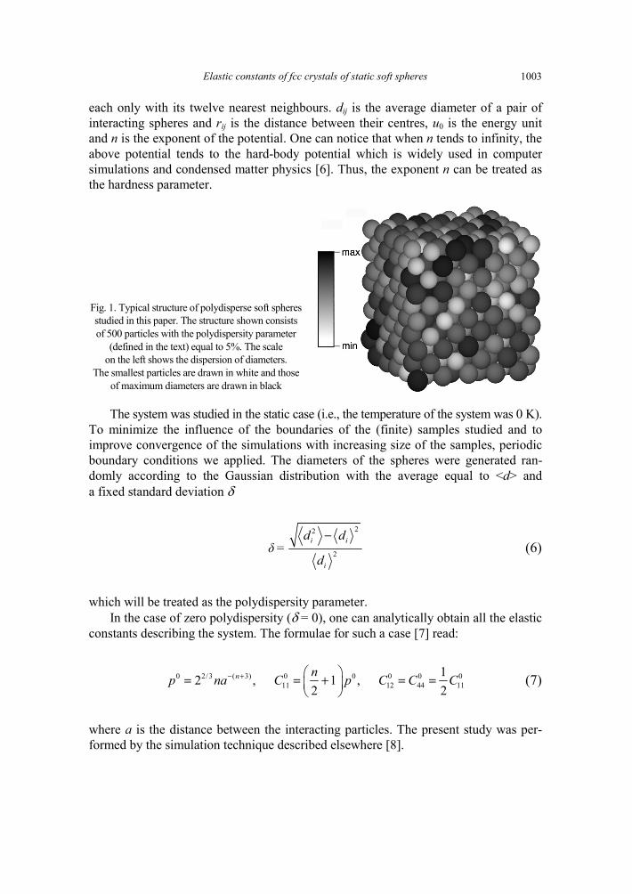
Elastic constants of fcc crystals of static soft spheres 1003
each only with its twelve nearest neighbours. dij is the average diameter of a pair of interacting spheres and rij is the distance between their centres, u0 is the energy unit and n is the exponent of the potential. One can notice that when n tends to infinity, the above potential tends to the hard-body potential which is widely used in computer simulations and condensed matter physics [6]. Thus, the exponent n can be treated as the hardness parameter.
Fig. 1. Typical structure of polydisperse soft spheres studied in this paper. The structure shown consists of 500 particles with the polydispersity parameter
(defined in the text) equal to 5%. The scale on the left shows the dispersion of diameters.
The smallest particles are drawn in white and those of maximum diameters are drawn in black
The system was studied in the static case (i.e., the temperature of the system was 0 K). To minimize the influence of the boundaries of the (finite) samples studied and to improve convergence of the simulations with increasing size of the samples, periodic boundary conditions we applied. The diameters of the spheres were generated ran-domly according to the Gaussian distribution with the average equal to <d> and a fixed standard deviation δ
22
2
i i
i
d dδ=
d
− (6)
which will be treated as the polydispersity parameter. In the case of zero polydispersity (δ = 0), one can analytically obtain all the elastic
constants describing the system. The formulae for such a case [7] read:
0 2/3 ( 3) 0 0 0 0 011 12 44 11
12 , 1 ,2 2
n np na C p C C C− + ⎛ ⎞= = + = =⎜ ⎟⎝ ⎠
(7)
where a is the distance between the interacting particles. The present study was per-formed by the simulation technique described elsewhere [8].
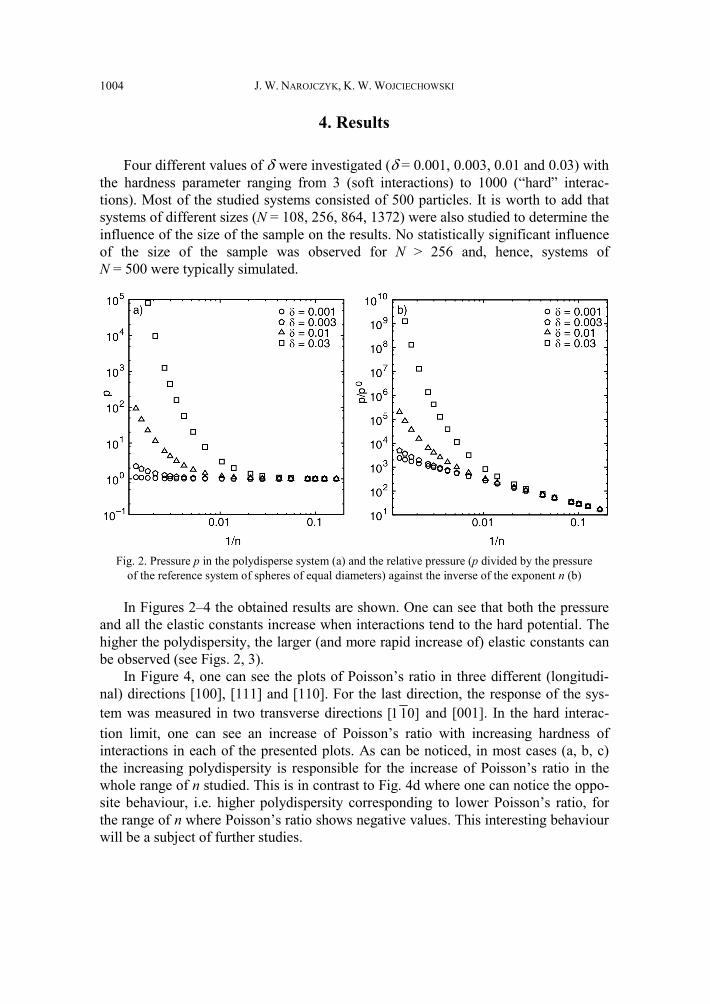
J. W. NAROJCZYK, K. W. WOJCIECHOWSKI 1004
4. Results
Four different values of δ were investigated (δ = 0.001, 0.003, 0.01 and 0.03) with the hardness parameter ranging from 3 (soft interactions) to 1000 (“hard” interac-tions). Most of the studied systems consisted of 500 particles. It is worth to add that systems of different sizes (N = 108, 256, 864, 1372) were also studied to determine the influence of the size of the sample on the results. No statistically significant influence of the size of the sample was observed for N > 256 and, hence, systems of N = 500 were typically simulated.
Fig. 2. Pressure p in the polydisperse system (a) and the relative pressure (p divided by the pressure
of the reference system of spheres of equal diameters) against the inverse of the exponent n (b)
In Figures 2–4 the obtained results are shown. One can see that both the pressure and all the elastic constants increase when interactions tend to the hard potential. The higher the polydispersity, the larger (and more rapid increase of) elastic constants can be observed (see Figs. 2, 3).
In Figure 4, one can see the plots of Poisson’s ratio in three different (longitudi-nal) directions [100], [111] and [110]. For the last direction, the response of the sys-tem was measured in two transverse directions [1 10] and [001]. In the hard interac-tion limit, one can see an increase of Poisson’s ratio with increasing hardness of interactions in each of the presented plots. As can be noticed, in most cases (a, b, c) the increasing polydispersity is responsible for the increase of Poisson’s ratio in the whole range of n studied. This is in contrast to Fig. 4d where one can notice the oppo-site behaviour, i.e. higher polydispersity corresponding to lower Poisson’s ratio, for the range of n where Poisson’s ratio shows negative values. This interesting behaviour will be a subject of further studies.
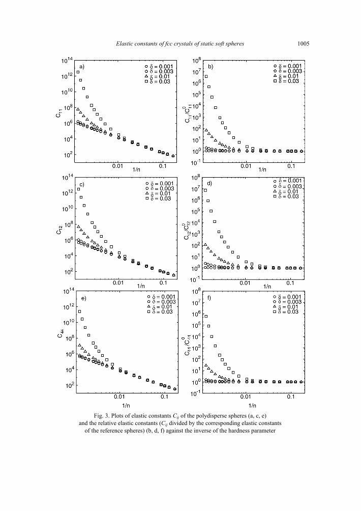
Elastic constants of fcc crystals of static soft spheres 1005
Fig. 3. Plots of elastic constants Cij of the polydisperse spheres (a, c, e) and the relative elastic constants (Cij divided by the corresponding elastic constants
of the reference spheres) (b, d, f) against the inverse of the hardness parameter
J. W. NAROJCZYK, K. W. WOJCIECHOWSKI 1006
Fig 4. Plots of Poisson’s ratio against the inverse of the hardness parameter in the following longitudinal directions: a) [100] b) [111] and c, d) [110] where the transverse directions are c) [001] and d) [110] ]
5. Conclusions
The presented numerical studies reveal that disorder (in the form of size polydis-persity) has essential influence on the elastic properties of the soft sphere systems. All the elastic constants grow with increasing polydispersity parameter as well as with increasing hardness of the interparticle interactions.
It is interesting to extend similar research to other three-dimensional systems of spherical particles and ‘molecules’ formed of them. It is also of interest to determine the influence of other types of structural disorder (e.g., degeneracy of the ground states of such systems [9]) on the elastic constants. Such studies will be a subject of our fu-ture work.
Elastic constants of fcc crystals of static soft spheres 1007
Acknowledgements
This work was supported by the Polish Office for Science and Higher Education, grant No. N20207032 /1512 (2007–2010).
References
[1] VAN BLAADEREN A., MRS Bull., 29 (2004), 85. [2] MANOHARAN V.N., PINE D.J., MRS Bull., 29 (2004), 91. [3] WOJCIECHOWSKI K.W., ALDERSON A., ALDERSON K.L., MARUSZEWSKI B., SCARPA F., Phys. Stat. Sol.
(b), 244 (2007), 813. [4] WOJCIECHOWSKI K.W., Comp. Meth. Sci. Technol., 11(2) (2005), 73. [5] KOWALIK M., WOJCIECHOWSKI K.W., J. Non.-Cryst. Sol., 325 (2006), 4269. [6] WOJCIECHOWSKI K.W., TRETIAKOV K.V., KOWALIK M., Phys. Rev. E, 67 (2003), 0361211. [7] TRETIAKOV K.V., WOJCIECHOWSKI K.W., J. Chem. Phys., 123 (2005), 074509. [8] NAROJCZYK J.W., WOJCIECHOWSKI K.W., Phys. Stat. Sol. (b), 244 (2007), 943. [9] WOJCIECHOWSKI K.W., NAROJCZYK J.W., Rev. Adv. Mater. Sci., 12 (2006), 120.
Received 7 May 2007 Revised 30 September 2007
Materials Science-Poland, Vol. 26, No. 4, 2008
Conductivity of a disordered ferromagnetic monoatomic film
A. PAJA*, B. J. SPISAK
Faculty of Physics and Applied Computer Science, AGH University of Science and Technology, al. Mickiewicza 30, 30-059 Cracow, Poland
Electron transport in the plane of a monoatomic metallic layer with non-zero magnetization is consi-dered. The material is represented by a two-dimensional set of disordered potentials which also possess spins aligned along one axis but not necessarily oriented in one direction. Such a system can be treated as a two-component alloy. The effective cross-section for conduction electrons has been calculated. The total conductivity is obtained within two-current model.
Key words: electron transport; thin films; disordered material; ferromagnet
1. Introduction
The study of electron transport properties of very thin magnetic films is very impor-tant for constructing nanodevices. Of particular interest is the problem of the resistivity anisotropy in such systems. Camley and Barnaś [1] gave theoretical description of the giant magnetoresistance effects in magnetic multilayers with antiferromagnetic struc-tures using the Boltzmann equation formalism. They explained these effects taking into account roughness of the interfaces and the asymmetry in spin-up and spin-down scat-tering but they assumed no disorder within the layers. In this work, we consider the con-ductivity of a monoatomic disordered layer with spontaneous magnetization where the above-mentioned asymmetry of the spin scattering plays a crucial role.
2. Theoretical model
We consider the magnetic monolayer as a system of disordered potentials which additionally have spins aligned along the axis determined by the resultant magnetiza- __________
*Corresponding author, e-mail: [email protected]
A. PAJA, B. J. SPISAK 1010
tion. We assume the current to flow along this axis. It actually consists of two currents of electrons polarized up and down. We calculate the behaviour of these types of car-riers separately and then compose the total conductivity.
We assume the total potential U(r) to be a sum of two parts
( ) ( ) ( )1 2U U U z= +r ρ (1)
where ρ is the position vector in the xy plane, U1(ρ) is a random set of atomic poten-tials, and U2(z) represents a geometrical confinement in the z direction [2]. The wave function of electron now can be factorized as follows
( ) ( ) ( ) ( )s z sψ ϕ ζ χ=r ρ (2)
where χ(s) represents its spin part and s is the spin index (s = ±1). The interaction of the electron spin s with the spin S of an atom at the position Ri can be described by the operator uS(Ri) included in the atomic potential
( ) ( ) ( )11
N
a i S ii
U u u=
= −∑ R Rρ ρ (3)
where ua(ρ – Ri) is the usual atomic potential of the ion located at Ri. We define the operator uS(Ri) by its matrix elements
( ) ( ) ( ) ( ) ( ) ( )( ) ( ) ( ) ( ) ( ) ( )
1 1
1 1
1 1 1, 1 1 0
1 1 0, 1 1i i
i i
u u
u u t
χ χ χ χχ χ χ χ
+ +
+ +
⎧ + + = − + =⎪⎨
+ − = − − =⎪⎩
R R
R R (4)
where the parameter t > 1. Physically it means that the electron which has its spin di-rected in accordance with that of an ion scatters only from the Coulomb potential while the electron of opposite spin scatters t times stronger. Spin flip during the scat-tering is here excluded. Matrix elements of u–1(Ri) are given by relations analogous with Eq. (4). In general, we can write
( ) ( ) ( ) ( )( )1S i ss Sss u s t tχ χ δ δ′ ′′ = + −R (5)
We now treat the magnetic material consisting of chemically identical atoms which differ with their direction of spin as a disordered binary alloy and apply the scheme of calculation analogous to the Faber–Ziman one [3]. We must take into ac-count that the scattering goes in the plane xy and the Fermi sphere is replaced by a circular sheet of radius kρ [2, 4, 5]. Let us consider the current of electrons of spin “up”. The differential cross-section for scattering of these carriers in plane is [2]
( ) ( ) ( )2
2* 21 1 12
18π 2π
d m U dd kσ ψ ψφ+
+ +
⎛ ⎞= ⎜ ⎟
⎝ ⎠∫
ρ
ρ ρ ρ ρ (6)
We assume the wave functions in the first Born approximation
Conductivity of a disordered ferromagnetic monoatomic film 1011
( ) ( ) ( )1 exp 1iψ χ+ = +kρρ ρ (7)
Inserting Eq. (7) into Eq. (6) and making use of Eqs. (4), we obtain
( ) ( ) ( ) ( ) ( )2
1/22 21 11 1 2 12 2 222
1 28π 2π a
d m u q N c S q c c tS q c t S qd kσϕ+ ⎛ ⎞ ⎡ ⎤= + +⎜ ⎟ ⎣ ⎦⎝ ⎠ρ
(8)
where ua(q) is the Fourier transform of the atomic potential ua(ρ – Ri), ′= −ρ ρq k k is the scattering vector in the xy plane, N is the total number of atoms, and Sik are the Ashcroft–Langreth structure factors. The coefficients c1 and c2 are the atomic fractions of atoms with spins “up” and “down”, respectively, and can be exactly expressed by the relative magnetization μ
1 21 1,
2 2c cμ μ+ −= = (9)
The transport relaxation time can now be calculated using the general formula for in-plane transport given in [2] as
( ) ( )
( ) ( ) ( ) ( )12
22
20
21 11 1 2 12 2 22
1 1 1 cos4π 2π
2
F atr
m nv d u qk
c S q c c tS q c t S q
π
ϕ ϕτ +
⎛ ⎞= −⎜ ⎟
⎝ ⎠
⎡ ⎤× + +⎣ ⎦
∫ρ (10)
where vF is the Fermi velocity, n is the area concentration of atoms, and q is related with ϕ by the formula
2 sin2
q k ϕ= ρ (11)
The transport relaxation time for inversely polarized electrons is
( ) ( )
( ) ( ) ( ) ( )
22
20
1/221 11 1 2 12 2 22
1 1 1 cos4π 2π
2
F atr
m nv d u qk
c t S q c c tS q c S q
π
ϕ ϕτ −
⎛ ⎞= −⎜ ⎟
⎝ ⎠
⎡ ⎤× + +⎣ ⎦
∫ρ (12)
The conductivity in the two-band model reads
1 1σρ ρ+ −
= + (13)
where
±±
± =tr
z
enmLτ
ρ 2 (14)
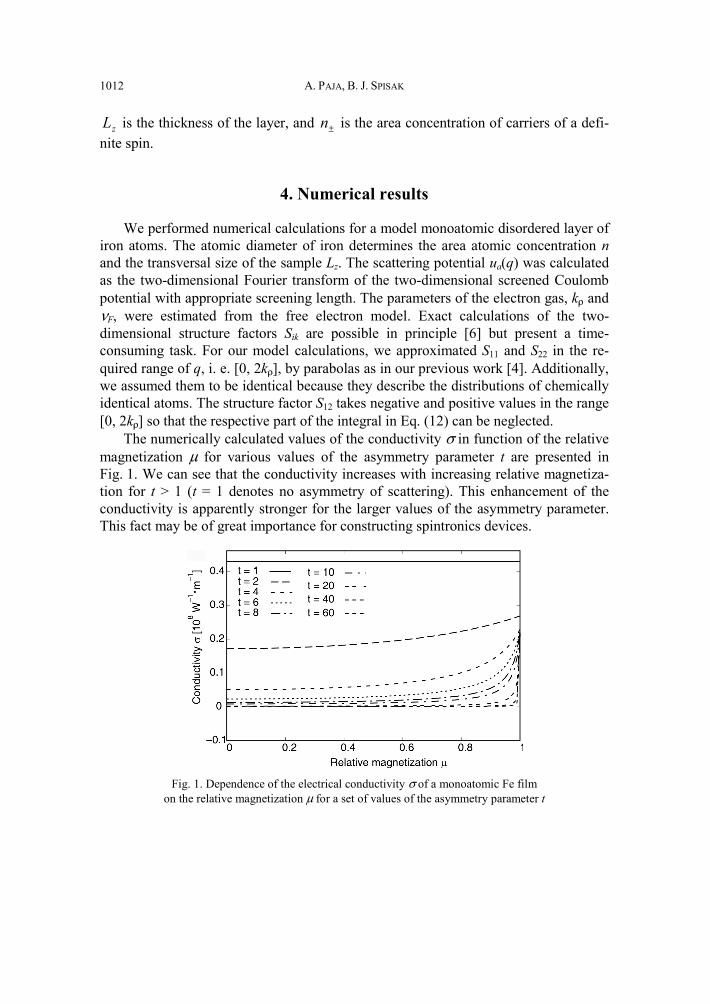
A. PAJA, B. J. SPISAK 1012
zL is the thickness of the layer, and ±n is the area concentration of carriers of a defi-nite spin.
4. Numerical results
We performed numerical calculations for a model monoatomic disordered layer of iron atoms. The atomic diameter of iron determines the area atomic concentration n and the transversal size of the sample Lz. The scattering potential ua(q) was calculated as the two-dimensional Fourier transform of the two-dimensional screened Coulomb potential with appropriate screening length. The parameters of the electron gas, kρ and νF, were estimated from the free electron model. Exact calculations of the two-dimensional structure factors Sik are possible in principle [6] but present a time-consuming task. For our model calculations, we approximated S11 and S22 in the re-quired range of q, i. e. [0, 2kρ], by parabolas as in our previous work [4]. Additionally, we assumed them to be identical because they describe the distributions of chemically identical atoms. The structure factor S12 takes negative and positive values in the range [0, 2kρ] so that the respective part of the integral in Eq. (12) can be neglected.
The numerically calculated values of the conductivity σ in function of the relative magnetization μ for various values of the asymmetry parameter t are presented in Fig. 1. We can see that the conductivity increases with increasing relative magnetiza-tion for t > 1 (t = 1 denotes no asymmetry of scattering). This enhancement of the conductivity is apparently stronger for the larger values of the asymmetry parameter. This fact may be of great importance for constructing spintronics devices.
Fig. 1. Dependence of the electrical conductivity σ of a monoatomic Fe film on the relative magnetization μ for a set of values of the asymmetry parameter t
Conductivity of a disordered ferromagnetic monoatomic film 1013
On the other hand, our model allows us to determine the parameter t provided the other parameters of the system are known.
4. Conclusions
The obtained formula allows us to calculate conductivity (or resistivity) of a monolayer film provided all involved physical quantities are known. The only one unknown parameter is t, which measures the asymmetry of the spin scattering. It can be estimated from fitting our formula to the experimentally obtained dependence of the conductivity on magnetization. The knowledge of the parameter t may be impor-tant for constructing spintronics devices of desired properties.
Acknowledgements
Financial support from the statutory funds of the Faculty of Physics and Applied Computer Science is gratefully acknowledged.
References
[1] CAMLEY R. E. AND BARNAŚ J., Phys. Rev. Lett., 63 (1989), 664. [2] SPISAK B. J. AND PAJA A., Mol. Phys. Rep., 40 (2004),144. [3] FABER T. E. AND ZIMAN J. M., Phil. Mag. 11 (1965) 153 [4] SPISAK B. J. AND PAJA A., Mater. Sci.-Poland, 24 (2006), 605. [5] BALCERZAK T., Thin Solid Films 500 (2006), 341. [6] JARGUZ P., PAJA A., Mater. Sci.-Poland, 24 (2006), 633.
Received 7 May 2007 Revised 24 September 2007
Materials Science-Poland, Vol. 26, No. 4, 2008
Ab intio study of YNi4Si under pressure
M. PUGACZOWA-MICHALSKA*, M. FALKOWSKI, A. KOWALCZYK
Institute of Molecular Physics, Polish Academy of Sciences, ul. Smoluchowskiego 17, 60-179 Poznań, Poland
In the framework of the density functional theory, we study conditions of formation of YNi4Si and its electronic properties under pressure. Within the local density approximation (LDA) used in calcula-tion, the equilibrium volume and the bulk modulus are obtained. The theoretical electronic specific heat coefficient γ (12.32 mJ/(f.u.·mol·K2)) derived from the density of states at the Fermi energy at ambient pressure and the experimental value of γ (13 mJ/(mol·K2)) are in a reasonable agreement.
Key words: rare earth metals; transition metal compounds; equation of states; electronic specific heat coefficient
1. Introduction
In recent years, interest has steadily increased in investigation of ternary com-pounds containing a rare earth metal and 3d transition element. These compounds may exhibit various ground state properties [1–4]. The studied compound YNi4Si belongs to a wide class of ternary compounds with rare earth metal crystallising in the hexago-nal CaCu5 structure with the space group P6/mmm. In the CaCu5 structure, Ni atoms occupy two kinds of crystallographic sites (2c) and (3g), the rare earth metal is located in (1a), and silicon occupies (3g).
By investigating the electronic structure of this class of materials, one can create the basis for understanding the majority of their physical properties. YNi4Si is indeed useful as an isostructural nonmagnetic reference material. Therefore, it is important to characterise its ground state properties and to consider what happens in the electronic structure under pressure using ab initio method.
__________
*Corresponding author, e-mail: [email protected]
M. PUGACZOWA-MICHALSKA et al. 1016
2. Experimental and calculation details
The sample preparation procedure for YNi4Si is almost the same as that for YNi4Cu [6]. The compound was synthesized by the induction melting of stoichiome-tric amounts of the constituent elements in a water-cooled boat. Argon was used as a protective atmosphere. The ingot was inverted and melted several times to insure homogeneity. According to X-ray diffraction data, the crystal structure of YNi4Si is of the hexagonal CaCu5 structure with the space group P6/mmm. The experimental lattice constants are a = 4.79 Å and c = 4.692 Å.
The electronic structure was calculated by the spin polarised tight binding linear muffin tin orbital (TB LMTO) method in the atomic sphere approximation (ASA) [7]. The systematic errors due to the use of ASA get cancelled while determining the ground state energy differences such as formation energy as well as incorporating the so-called ‘combined corrections’ one can partly salvage the error due to spheridisation of potential and charge density [7, 8]. For the exchange-correlation potential, the von Barth–Hedin parameterisation [9] has been employed. The Langreth–Mehl–Hu non-local correction [10] was included. All total energy for above 1220 k points is con-tained in the irreducible Brillouin zone. The initial atomic configurations for each atom were taken as in the periodic table of elements. We assume for Y core(Kr) + 4d15s2, for Ni: core(Ar) + 3d84s2 and for Si: core(Ne) + 2s22p2. The primi-tive cell consists of 6 atoms, where Y atom occupies (1a) site, four Ni atoms are in (2c), (3g) positions, and Si atom is in the (3g) or (2c) positions.
3. Results
Based on the self-consistent calculations, the ground state of YNi4Si is concluded a paramagnetic one. The equilibrium lattice constants obtained by minimization pro-cedure of the total energy of YNi4Si are a = 4.551 Å, c = 4.41 Å, where Si atom occu-pied (3g) position in CaCu5 structure. This result is in the acceptable range of LDA band structure calculations.
To analyze the stability of YNi4Si, a possibility of occupation of (2c) position by Si atom was also considered in CaCu5 structure. The results of the total energy calcu-lations for YNi4Si indicate that substitution of Ni by Si takes place in (3g) position rather than in the (2c) site. The corresponding difference in the total energy is 30.2 mRy/atom. We used the cohesive energy as an important physical quantity, ex-pressing the strength of the force binding atoms together in the compound. Thus, it is correlative with the structural stability in the ground state. The cohesive energy per formula unit of YNi4Si is obtained by ( ) ( )coh total 4( ) 4 Ni Si (YNi Si)E E Y E E E= + + − (1)
where Etotal(YNi4Si) refers to the total energy of the intermetallic compound at equilib-rium, and E(Y), E(Ni), E(Si) are the total energies of pure atomic components. The
Ab intio study of YNi4Si under pressure 1017
values of cohesive energy for YNi4Si with two different positions of Si atom in the unit cell, listed in Table 1, show that the both occupations of Si are possible, but the (3g) position in CaCu5 structure is more preferable.
Table 1. Equilibrium lattice parameters, cohesive energy and density of states at the Fermi energy of YNi4Si for two possible occupations of Si atom in the unit cell
Position 3g 2c a [Å] 4.551 4.567 c [Å] 4.410 4.425 Ecoh [Ry/f.u.] 20.15 19.97 N(EF) [states/(Ry f.u.)] 71.21 106.14
The results of ab initio study allow us to predict the pressure behaviour of YNi4Si
at T = 0 K. We use the bulk modulus as a characteristic change in volume of a solid sample as the pressure on it is changed. The bulk modulus is defined as:
( )2tot
0 2
E VpB V VV V
∂∂= − =∂ ∂
(2)
where p is the pressure and V is volume of the cell. The volume–energy dependence is fitted by the Murnaghan equation of state (EOS) [11]:
( ) 0 0 0total 01 1
( 1)
BB V V VE V B EB B V V
′⎡ ⎤⎛ ⎞ ⎛ ⎞′= + − − +⎢ ⎥⎜ ⎟ ⎜ ⎟′ ′ − ⎝ ⎠ ⎝ ⎠⎢ ⎥⎣ ⎦ (3)
Here Etotal(V) is the total energy of the system at volume V, B0 and B′ are the bulk modulus and its pressure derivative at the equilibrium volume V0, respectively. Thus, for YNi4Si, the bulk modulus and its pressure derivative are B0 = 143 GPa and B′ = 1.37, respectively. The obtained value of B0 for YNi4Si is lower than that for ear-lier studied YNi4B (about 162 GPa) [5] and YNi4Cu (160 GPa) [6]. Thus, one can expect that YNi4Si is more compressible material than isostructural YNi4Cu and YNi4B with CeCo4B structure. The difference between the values of the bulk moduli of YNi4Si and earlier studied YNi4B is connected with two features: 1) the structural differences between both compounds (the unit cell of YNi4B contains two formula units); 2) one of constituents (B atom) in YNi4B has the bulk modulus higher than a silicon atom. In the case of YNi4Cu, the electronic structure and nearly filled 3d bands of Cu in particular have a significant influence on the value of compressibility.
The theoretical pressure–volume dependence for studied YNi4Si calculated as the negative volume derivative of the total energy:
EpV∂= −∂
(4)
is shown in Fig. 1. The picture of the isothermal (at T = 0 K) volume–pressure de-pendence shows that the applied hydrostatic pressure of 22.6 GPa caused the change of volume of YNi4Si from equilibrium volume to 0.87 of its value.
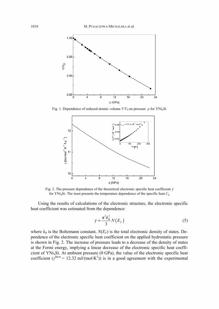
M. PUGACZOWA-MICHALSKA et al. 1018
Fig. 1. Dependence of reduced atomic volume V/V0 on pressure p for YNi4Si
Fig. 2. The pressure dependence of the theoretical electronic specific heat coefficient γ
for YNi4Si. The inset presents the temperature dependence of the specific heat Cp
Using the results of calculations of the electronic structure, the electronic specific heat coefficient was estimated from the dependence:
( )2 2π3
BF
k N Eγ = (5)
where kB is the Boltzmann constant, N(EF) is the total electronic density of states. De-pendence of the electronic specific heat coefficient on the applied hydrostatic pressure is shown in Fig. 2. The increase of pressure leads to a decrease of the density of states at the Fermi energy, implying a linear decrease of the electronic specific heat coeffi-cient of YNi4Si. At ambient pressure (0 GPa), the value of the electronic specific heat coefficient (γtheor = 12.32 mJ/(mol·K2)) is in a good agreement with the experimental
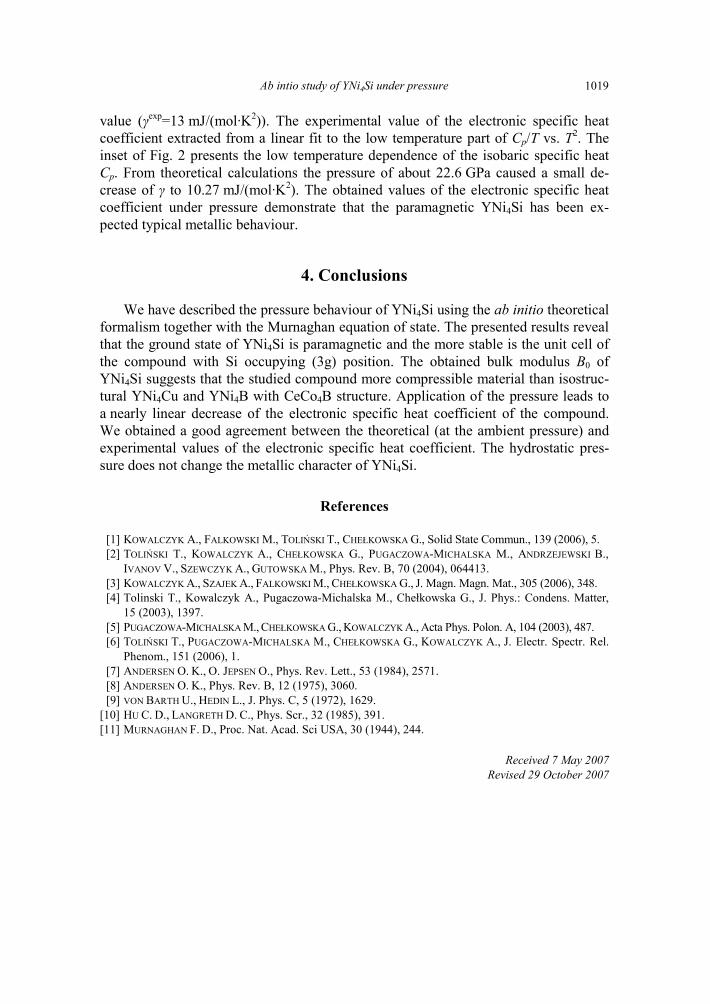
Ab intio study of YNi4Si under pressure 1019
value (γexp=13 mJ/(mol·K2)). The experimental value of the electronic specific heat coefficient extracted from a linear fit to the low temperature part of Cp/T vs. T2. The inset of Fig. 2 presents the low temperature dependence of the isobaric specific heat Cp. From theoretical calculations the pressure of about 22.6 GPa caused a small de-crease of γ to 10.27 mJ/(mol·K2). The obtained values of the electronic specific heat coefficient under pressure demonstrate that the paramagnetic YNi4Si has been ex-pected typical metallic behaviour.
4. Conclusions
We have described the pressure behaviour of YNi4Si using the ab initio theoretical formalism together with the Murnaghan equation of state. The presented results reveal that the ground state of YNi4Si is paramagnetic and the more stable is the unit cell of the compound with Si occupying (3g) position. The obtained bulk modulus B0 of YNi4Si suggests that the studied compound more compressible material than isostruc-tural YNi4Cu and YNi4B with CeCo4B structure. Application of the pressure leads to a nearly linear decrease of the electronic specific heat coefficient of the compound. We obtained a good agreement between the theoretical (at the ambient pressure) and experimental values of the electronic specific heat coefficient. The hydrostatic pres-sure does not change the metallic character of YNi4Si.
References
[1] KOWALCZYK A., FALKOWSKI M., TOLIŃSKI T., CHEŁKOWSKA G., Solid State Commun., 139 (2006), 5. [2] TOLIŃSKI T., KOWALCZYK A., CHEŁKOWSKA G., PUGACZOWA-MICHALSKA M., ANDRZEJEWSKI B.,
IVANOV V., SZEWCZYK A., GUTOWSKA M., Phys. Rev. B, 70 (2004), 064413. [3] KOWALCZYK A., SZAJEK A., FALKOWSKI M., CHEŁKOWSKA G., J. Magn. Magn. Mat., 305 (2006), 348. [4] Tolinski T., Kowalczyk A., Pugaczowa-Michalska M., Chełkowska G., J. Phys.: Condens. Matter,
15 (2003), 1397. [5] PUGACZOWA-MICHALSKA M., CHEŁKOWSKA G., KOWALCZYK A., Acta Phys. Polon. A, 104 (2003), 487. [6] TOLIŃSKI T., PUGACZOWA-MICHALSKA M., CHEŁKOWSKA G., KOWALCZYK A., J. Electr. Spectr. Rel.
Phenom., 151 (2006), 1. [7] ANDERSEN O. K., O. JEPSEN O., Phys. Rev. Lett., 53 (1984), 2571. [8] ANDERSEN O. K., Phys. Rev. B, 12 (1975), 3060. [9] VON BARTH U., HEDIN L., J. Phys. C, 5 (1972), 1629.
[10] HU C. D., LANGRETH D. C., Phys. Scr., 32 (1985), 391. [11] MURNAGHAN F. D., Proc. Nat. Acad. Sci USA, 30 (1944), 244.
Received 7 May 2007 Revised 29 October 2007
Materials Science-Poland, Vol. 26, No. 4, 2008
Study of ultrathin Co films grown on Si(111) substrates
A. STUPAKIEWICZ1, 2∗, A. FLEURENCE2, R. GIENIUSZ1, A. MAZIEWSKI1, T. MAROUTIAN2, P. GOGOL2, B. BARTENLIAN2, R. MÉGY2, P. BEAUVILLAIN2
Laboratory of Magnetism, University of Białystok, ul. Lipowa 41, 15-424 Białystok, Poland 2Institut d’Electronique Fondamentale, Universite Paris XI, CNRS, UMR 8622, F-91405 Orsay, France
Ultrathin Co films were grown on vicinal Si(111) substrate with Cu buffer layers. Room temperature ferromagnetic behaviour of Co layer thicker than 4 monolayers was confirmed by the magneto-optical Kerr effect. Ferromagnetic resonance measurements have proven the coexistence of the magnetocrystal-line anisotropy along with the growth- and vicinal induced uniaxial out-of-plane and in-plane contribu-tions. Multi-jump hysteresis loops were observed for selected in-plane orientations of magnetic field which is explained by the competition of different anisotropy contributions.
Key words: magnetic anisotropy; ultrathin films; cobalt; vicinal substrate
1. Introduction
Ultrathin magnetic materials have been intensively investigated due to their inter-esting physical properties and technological application. Vicinal substrates are very popular templates for the self-organized growth of magnetic nanostructures and nano-particles [1, 2]. In the case of growth of a thin magnetic film, the vicinality induces new terms in the expression of the magnetic anisotropy energy. When the film is grown on a stepped surface [3–6], the following contributions to magnetic anisotropy are usually considered: the magnetocrystalline, shape, and both out-of plane and in-plane uniaxial magnetic anisotropies.
In the present work, we investigate the magnetization reversal and magnetic aniso-tropy of ultrathin Co films grown on vicinal Si(111) substrates. Due to a strong reac-tivity between Co and Si, cobalt is deposited on a Cu buffer layer. The growth of co-balt on copper substrates has been intensively studied because the fcc Co crystalline structure can be stabilized [7]. The combination of cubic magnetocrystalline anisotro-
__________
∗Corresponding author, e-mail: [email protected]
A. STUPAKIEWICZ et al. 1022
py with step induced anisotropy was studied in the Co/Cu(001) system [3, 8]. Howev-er, a systematic study on Co/Cu(111) films has not been carried out.
2. Experimenal details
The following structures were deposited by molecular beam epitaxy on a vicinal Si(111) substrate with 2° misorientation towards the [ 1 12] direction. The surface was prepared under ultra high vacuum by direct current heating up to 1250 °C for a few seconds. The temperature was checked using a thermocouple up to 550 °C and by infrared pyrometer above. As seen by STM after preparation, the surface is constituted of monoatomic steps separated by 7×7 reconstructed terraces [9]. Step-edge orienta-tion on the substrate was along the [1 10] Si direction. The buffer layer of 4 Cu mono-layers (MLs) was deposited at 100 °C and was expected to form Cu silicide [10]. Our previous investigations by the second harmonic generation technique [11] showed that Cu coverage reproduces vicinal character of the Si substrate. 3, 5, 7 and 15 MLs of Co were then deposited at room temperature (RT) on the Cu surface. Finally a 30 ML Au capping layer was grown at RT.
Measurements were performed at RT using a magneto-optical Kerr effect (MOKE) based magnetometer and ferromagnetic resonance (FMR) X-band spectro-meter. The MOKE magnetometer with laser light of λ = 640 nm enabled determination of the Kerr rotation and ellipticity for both polar (p-MOKE) and longitudinal (l-MOKE) experimental configurations. The measurements of the l-MOKE hysteresis loops were performed with the magnetic field applied at different azimuthal orientations defined by ϕΗ , the angle in the plane of the sample referenced from miscut direction.
3. Results and discussion
The p-MOKE hysteresis loops for various Co thicknesses are presented in Fig. 1, pointing to the absence of ferromagnetism for the Co coverage below 5 ML. This may be explained by the formation of Co compounds with Cu and Si [12, 13]. Lowering of the Curie temperature is expected at such interfaces [4].
Out-of-plane magnetization components were observed for the 7 ML Co thick-ness. A canted magnetization state is deduced from the magnetization curves, as shown in the inset of Fig. 1. Mainly in-plane magnetization state is expected from p-MOKE loop measured for 15 ML Co.
The FMR technique is useful in a direct determination of the magnetic anisotropy. Measurements of the angular dependence of the resonance field (Hr) are related to the magnetic anisotropy constants and enable determination of the easy magnetization axes (minima in Hr). The experimental dependence of the resonance field Hr in func-tion of the angle ϕΗ for the 15 ML Co sample is shown in Fig. 2 (dots).
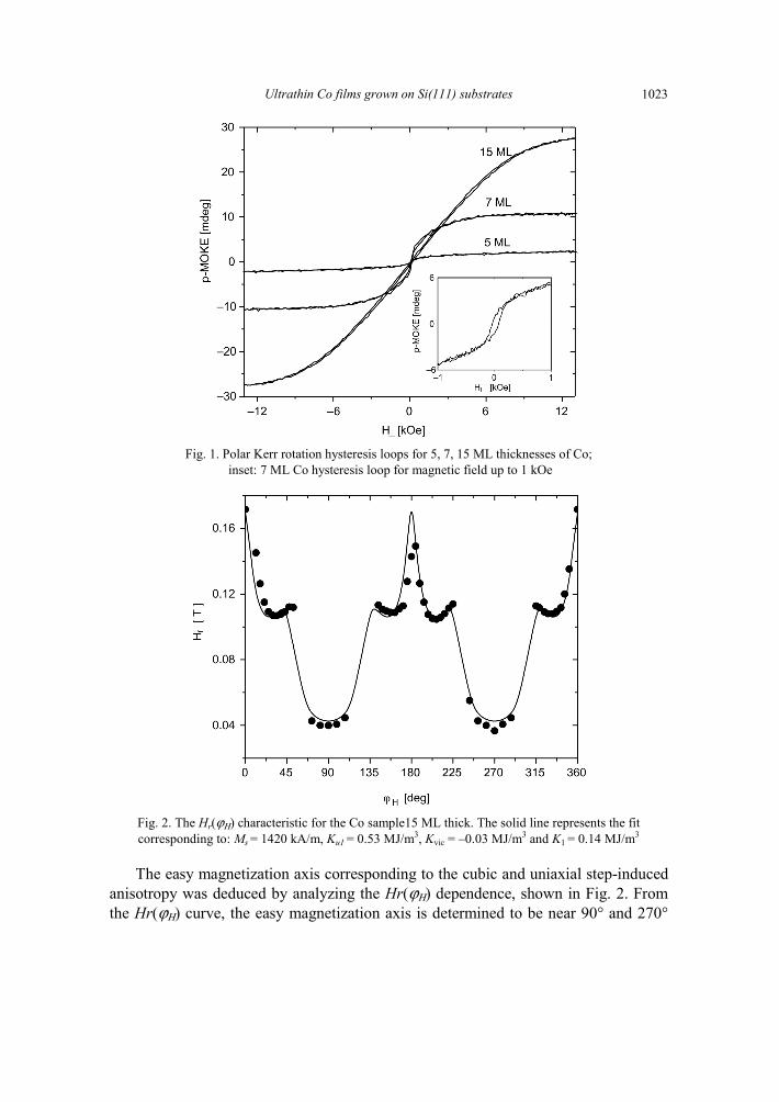
Ultrathin Co films grown on Si(111) substrates 1023
Fig. 1. Polar Kerr rotation hysteresis loops for 5, 7, 15 ML thicknesses of Co;
inset: 7 ML Co hysteresis loop for magnetic field up to 1 kOe
Fig. 2. The Hr(ϕΗ) characteristic for the Co sample15 ML thick. The solid line represents the fit corresponding to: Ms = 1420 kA/m, Ku1 = 0.53 MJ/m3, Kvic = –0.03 MJ/m3 and K1 = 0.14 MJ/m3
The easy magnetization axis corresponding to the cubic and uniaxial step-induced anisotropy was deduced by analyzing the Hr(ϕΗ) dependence, shown in Fig. 2. From the Hr(ϕΗ) curve, the easy magnetization axis is determined to be near 90° and 270°
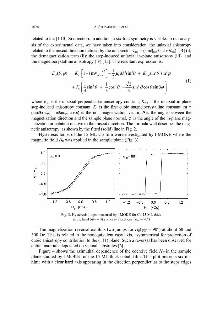
A. STUPAKIEWICZ et al. 1024
related to the [1 10] Si direction. In addition, a six-fold symmetry is visible. In our analy-sis of the experimental data, we have taken into consideration: the uniaxial anisotropy related to the miscut direction defined by the unit vector vmis = (sinθmis, 0, cosθmis) [14] (i); the demagnetization term (ii); the step-induced uniaxial in-plane anisotropy (iii) and the magnetocrystalline anisotropy (iv) [15]. The resultant expression is:
( )2 2 2 2 2
1 mis 0 vic
4 4 31
1( , ) 1 sin sin sin2
1 1 2 sin cos sin cos sin34 3 3
A u sE K M K
K
θ ϕ μ θ θ ϕ
θ θ θ θ ϕ
⎡ ⎤= − − +⎣ ⎦
⎛ ⎞+ + −⎜ ⎟⎜ ⎟
⎝ ⎠
mv
(1)
where Ku1 is the uniaxial perpendicular anisotropy constant, Kvic is the uniaxial in-plane step-induced anisotropy constant, K1 is the first cubic magnetocrystalline constant, m = (sinθcosϕ, sinθsinϕ, cosθ) is the unit magnetization vector, θ is the angle between the magnetization direction and the sample plane normal, ϕ is the angle of the in-plane mag-netization orientation relative to the miscut direction. The formula well describes the mag-netic anisotropy, as shown by the fitted (solid) line in Fig. 2.
Hysteresis loops of the 15 ML Co film were investigated by l-MOKE where the magnetic field HII was applied in the sample plane (Fig. 3).
Fig. 3. Hysteresis loops measured by l-MOKE for Co 15 ML thick in the hard (ϕΗ = 0) and easy directions (ϕΗ = 90o)
The magnetization reversal exhibits two jumps for HII(ϕΗ = 90°) at about 60 and 300 Oe. This is related to the nonequivalent easy axis, asymmetrical for projection of cubic anisotropy contribution to the (111) plane. Such a reversal has been observed for cubic materials deposited on vicinal substrates [6].
Figure 4 shows the azimuthal dependence of the coercive field HC in the sample plane studied by l-MOKE for the 15 ML thick cobalt film. This plot presents six mi-nima with a clear hard axis appearing in the direction perpendicular to the steps edges
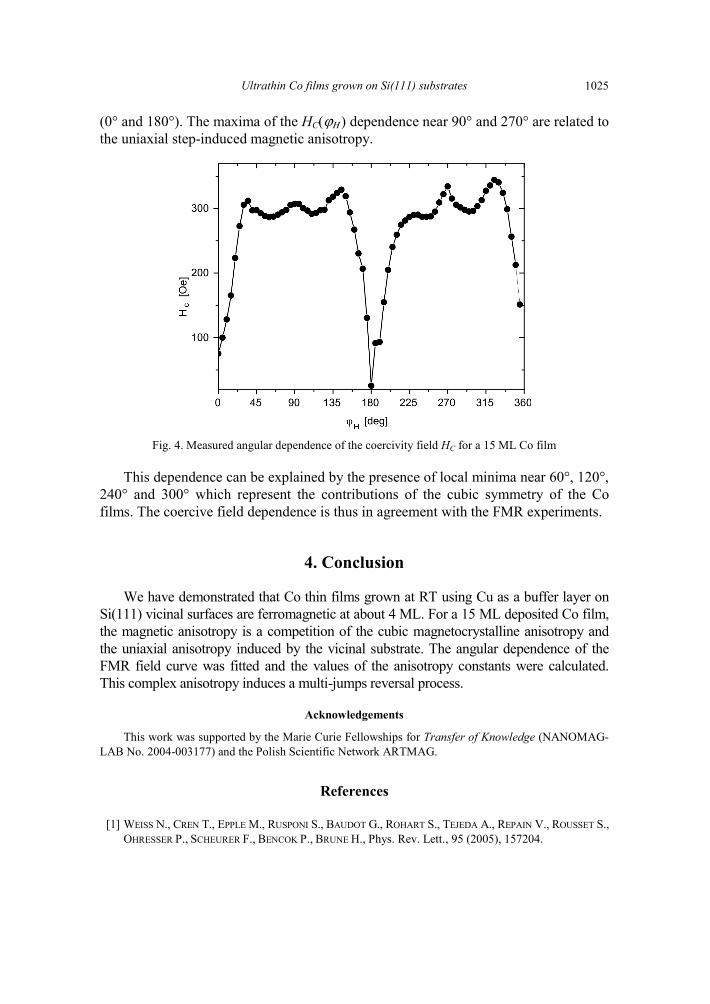
Ultrathin Co films grown on Si(111) substrates 1025
(0° and 180°). The maxima of the HC(ϕΗ ) dependence near 90° and 270° are related to the uniaxial step-induced magnetic anisotropy.
Fig. 4. Measured angular dependence of the coercivity field HC for a 15 ML Co film
This dependence can be explained by the presence of local minima near 60°, 120°, 240° and 300° which represent the contributions of the cubic symmetry of the Co films. The coercive field dependence is thus in agreement with the FMR experiments.
4. Conclusion
We have demonstrated that Co thin films grown at RT using Cu as a buffer layer on Si(111) vicinal surfaces are ferromagnetic at about 4 ML. For a 15 ML deposited Co film, the magnetic anisotropy is a competition of the cubic magnetocrystalline anisotropy and the uniaxial anisotropy induced by the vicinal substrate. The angular dependence of the FMR field curve was fitted and the values of the anisotropy constants were calculated. This complex anisotropy induces a multi-jumps reversal process.
Acknowledgements
This work was supported by the Marie Curie Fellowships for Transfer of Knowledge (NANOMAG-LAB No. 2004-003177) and the Polish Scientific Network ARTMAG.
References
[1] WEISS N., CREN T., EPPLE M., RUSPONI S., BAUDOT G., ROHART S., TEJEDA A., REPAIN V., ROUSSET S., OHRESSER P., SCHEURER F., BENCOK P., BRUNE H., Phys. Rev. Lett., 95 (2005), 157204.
A. STUPAKIEWICZ et al. 1026
[2] GAMBARDELLA P., DALLMEYER A., MAITI K., MALAGOLI M.C., EBERHARDT W., KERN K., CARBONE C., Nature 416 (2002), 301.
[3] KAWAKAMI R.K., BOWEN M.O., CHOI H.J., ESCORCIA-APARICIO E.J., QIU Z.Q., Phys. Rev. B, 58 (1998), R5924.
[4] HUANG F., KIEF M.T., MANKEY G.J., WILLIS R.F., Phys. Rev. B, 49 (1994), 3962. [5] BERGER A., LINKE U., OEPEN H.P., Phys. Rev. Lett., 68 (1992), 839. [6] COUGO DOS SANTOS M., GESHEV J., PEREIRA L.G., ALVES M.C.M., SCHMIDT J.E., Phys. Rev. B, 70
(2004), 104420. [7] FARLE M., PLATOW W., KOSUBEK E., BABERSCHKE K., Surf. Sci., 439 (1999), 146 and references
therein. [8] CINAL M., UMERSKY A., Phys. Rev. B, 73 (2006), 184423. [9] WEI J., WANG X.-S, GOLDBERG J.L., BARTELT N.C., WILLIAMS E.D., Phys. Rev. Lett., 68 (1992),
3885. [10] PEDERSEN K., KRISTENSEN T.B., PEDERSER T.G., MORGEN P., LI Z., HOFFMAN S.V., Phys. Rev. B, 66
(2002), 153406 [11] CHEIKH-ROUHOU W., SAMPAIO L.C., BARTENLIAN B., BEAUVILLAIN P., BRUN A., FERRÉ J., GEORGES P.,
JAMET J.P., MATHET V., STUPAKIEWICZ A., Appl. Phys. B, 74 (2002), 665. [12] RABE A., NEMMEL N., STELTENPOHL A., FAUSTER TH., Phys. Rev. Lett., 73 (1994), 2728. [13] PIRRI C., PERUCHETTI J.C., GEWINNER G., Phys. Rev. B., 29 (1984), 3391. [14] STUPAKIEWICZ A., GIENIUSZ R., MAZIEWSKI A., POSTAVA K., WAWRO A., BACZEWSKI L.T., phys. stat.
sol. (b), 243 (2006), 202. [15] STUPAKIEWICZ A., MAZIEWSKI A., GOGOL P., BEAUVILLAIN P., Physica B, 372 (2006), 354.
Received 7 May 2007 Revised 2 November 2007
Materials Science-Poland, Vol. 26, No. 4, 2008
Ground state phase diagram of a diluted fcc magnet with modified RKKY
interaction in an external magnetic field
K. SZAŁOWSKI*, T. BALCERZAK
Department of Solid State Physics, University of Łódź, ul. Pomorska 149/153, 90-236 Łódź, Poland
A model of a diluted fcc magnet with modified RKKY interaction in an external magnetic field has been considered. The stability regions of paramagnetic, ferromagnetic and some typical antiferromagnetic phases in the ground state have been studied. In particular, the influence of the dilution and the external field on the phase diagrams has been discussed.
Key words: diluted magnetic semiconductor; phase diagram; RKKY interaction
1. Introduction
In diluted magnetic semiconductors (DMS) such as (Ga,Mn)As which acquire fer-romagnetic properties owing to impurity ions [1, 2], the indirect coupling of magnetic moments via the Ruderman–Kittel–Kasuya–Yosida (RKKY) interaction is believed to contribute mainly to ferromagnetic ordering [3–5]. An immense importance of these materials serves as motivation to study the models of site-diluted fcc magnets driven by the RKKY interaction. A recent example is a Monte Carlo-based work [6] focused mainly on the ferromagnetic phase stability region. However, for the oscillatory, carri-er concentration-dependent nature of the interaction, the phase diagrams should indi-cate a variety of possible magnetic orderings, including antiferromagnetic phases such as presented in [7]. On the other hand, the ground-state phase diagrams for the RKKY interaction in the presence of an external magnetic field have not been studied so far. Therefore, the aim of the present paper is to fill the gap and to study these diagrams for the site-diluted model in the field.
The RKKY interaction is modified here by the damping factor responsible for the free-carriers localization, and by the short-range superexchange antiferromagnetic __________
*Corresponding author, e-mail: [email protected]
K. SZAŁOWSKI, T. BALCERZAK 1028
interaction. Such a model is a prototype which can be used to describe roughly the situation occurring in (Ga,Mn)As [6].
2. Theory
We consider a diluted magnet with fcc lattice where the localized spins occupy the lattice sites at random with an equal probability ni. The system is embedded in an ex-ternal magnetic field B oriented in the z direction. We assume the Ising-like Hamilto-nian in the form:
( )RKKY AFeff B
, , z z z z z
ij i j i j i j i j i ii j i j i
J r S S J S S g B Sξ ξ ξ ξ μ ξ′< > < >
= − − +∑ ∑ ∑H (1)
In Equation (1), the first summation is over all the site pairs (for the long-range RKKY indirect interaction), whereas the second summation is only for the nearest-neighbour (NN) superexchange antiferromagnetic interaction J AF. The third term incorporates the external field B. The occupation operators (ξI = 0, 1) describe the site dilution, so that the configurational averages ⟨…⟩r yield ⟨ξi⟩r = ni and 2.i j ir
nξ ξ ≈ The RKKY exchange
interaction in the spherical approximation is given in the form [8–11]:
( ) ( ) ( ) ( )( )
4 F F FRKKY /F 4
F
sin 2 2 cos 2 e
2rk r k r k r
J r C k ak r
λ−−= (2)
The Fermi wave vector kF for the fcc lattice is kF = (12π2nc)1/3/a, where a is the lat-tice constant, and nc stands for the free-carriers concentration. The energetic constant C in Eq. (2) is given by C = 2A2m*/(πh2a4), for the contact potential A and the effective mass of the carriers m*. The exponential damping factor, with the characteristic length λ, takes into account a possible localization of the carriers [11] in the inhomogeneous system.
In Equation (1), the effective gyromagnetic factor geff contains both the localized spin component, gS, and the factor of the free carriers, gc. As shown in the paper [12], the total effective gyromagnetic factor should be of the form:
*
eff 2c F
Sg m Akg g
h= +
The stable ground state magnetic phases under consideration include the disor-dered paramagnetic phase (P) as well as the ordered ferromagnetic (F) and three anti-ferromagnetic phases, which are characteristic of the fcc structure [13–15]. According to [13–15], the antiferromagnetic phases are the following: 1st kind (AF1), 1st kind improved (AF1), and 2nd kind (AF2) orderings. The stability regions of each phase in the ground state are determined by the enthalpy minimization, where the enthalpy H
Phase diagram of a diluted fcc magnet 1029
per one lattice site is defined by /r
H N= H , and ... is the thermal average in
the limit T → 0. For the Hamiltonian (1), the exact expression for the enthalpy is given in the form:
( ) ( ) ( )
( )
2 2 RKKY AF1 1
2 2 RKKY AF1 eff B
for AF phases
for F phase
1 2
1 2
0 for P phase
i k k kk
i k k ik
n S z z J r z z J
H n S z J r z J g n BSμ
↑↑ ↑↓ ↑↑ ↑↓⎧ ⎡ ⎤− − + −⎪ ⎢ ⎥⎣ ⎦⎪
⎪ ⎡ ⎤⎪= − + −⎨ ⎢ ⎥⎣ ⎦⎪
⎪⎪⎪⎩
∑
∑ (3)
In Equation (3), by kz↑↑ ( )kz↑↓ we denote the numbers of spins situated on the kth coordination zone of the radius rk which are parallel (antiparallel) to the central spin, where .k k kz z z↑↑ ↑↓= + These numbers are characteristic of (and different for) each or-dered phase in the fcc structure and have to be found numerically.
3. Numerical results and discussion
The ground state phase diagrams have been calculated based on the exact expres-sion (3), where the summation over k was performed up to rk = 100a (which corre-sponds to 18 335 coordination zones in the fcc structure). For such an interaction range, a good convergence of the enthalpy per site has been achieved. The phase dia-grams are presented in ni and nc/ni coordinates, where ni and nc are treated as inde-pendent variables, being concentrations of the impurity spins and free carriers, respec-tively. This assumption reflects the fact that in DMS both lattice and interstitial ions make independent contributions to (Ga, Mn)As.
In order to perform the numerical calculations in an external field, some experi-mental material constants characteristic of (Mn,Ga)As have been assumed such as: a = 5.65 Å, A = –55 meV·nm3 and m* = 0.5me, whereas the localized spins have the magnitude S = 5/2 [2, 16]. For the above values, we obtain the energetic constant C = 3.1 meV. Selected phase diagrams are presented in Fig. 1.
The diagram in Fig. 1a corresponds to the initial situation (without the external magnetic field), whereas the RKKY interaction is taken without any damping, i.e., for λ → ∞. The antiferromagnetic NN interaction has been neglected, J AF = 0. For these initial parameters, the phase boundaries are of hyperbolic shape. It is noteworthy that in the particular case, for ni = 1, the phases sequence upon nc (and the boundary posi-tions) are precisely the same as those calculated in [7]. In Figure 1b, an additional NN interaction is taken into account with some moderate magnitude J AF/C = –0.5. The re-maining parameters are the same as in Fig. 1a. We see that two new areas of AF1 phase appear for the low carrier concentrations and in the region between AF2 and AF1I
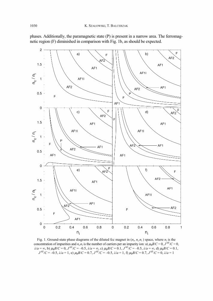
K. SZAŁOWSKI, T. BALCERZAK 1030
phases. Additionally, the paramagnetic state (P) is present in a narrow area. The ferromag-netic region (F) diminished in comparison with Fig. 1b, as should be expected.
Fig. 1. Ground-state phase diagrams of the diluted fcc magnet in (ni, nc/ni ) space, where ni is the concentration of impurities and nc/ni is the number of carriers per an impurity ion: a) μBB/C = 0, J AF/C = 0, λ/a = ∞, b) μBB/C = 0, JAF/C = –0.5, λ/a = ∞, c) μBB/C = 0.1, JAF/C = –0.5, λ/a = ∞, d) μBB/C = 0.1,
J AF/C = –0.5, λ/a = 1, e) μBB/C = 0.7, JAF/C = –0.5, λ/a = 1, f) μBB/C = 0.7, JAF/C = 0, λ/a = 1
Phase diagram of a diluted fcc magnet 1031
In Figure 1c, the effect of the external field of a moderate magnitude μBB/C = 0.1 is presented. The other parameters are the same as in Fig. 1b. The field restricts the AF1 and P phases and favours the F phase. The effect is most remarkable for the low concentration of carriers. On the other hand, the influence of the strong localization of the carriers is illustrated in Fig. 1d for λ/a = 1, whereas the other parameters are the same as in Fig.1c. It is worth noting that the effect of damping in the RKKY interac-tion is opposite to the external field influence, i.e., the AF1 phase grows with the damping at the expense of the F-phase. Additionally, the P phase disappears in Fig. 1d as a result of a strong localization of the carriers. On the other hand, when a relatively strong magnetic field is applied, i.e., μBB/C = 0.7 in Fig. 1e, the F phase becomes stronger at the expense of AF1 and AF2 phases. The influence of the external field is most remarkable in Fig. 1e for low concentrations of impurities ni, contrary to Fig. 1c, where the changes were mainly seen for low concentration of carriers nc.
Finally, in Fig. 1f the antiferromagnetic NN interaction has been removed, whereas the strong magnetic field and strong damping remained with the values as in Fig. 1e. As a consequence, the areas occupied by the F phase became considerably larger, while all the antiferromagnetic phases have been suppressed. In particular, one of the AF1 areas, indicated by the arrow in Fig. 1e, completely disappears in Fig. 1f. All the phase boundaries presented in the ground state correspond to the 1st order (discontinuous) phase transitions.
4. Conclusions
For the ground-state phase diagrams calculated without the external magnetic field (Figs. 1a and 1b), the phase boundaries are hyperbolic. By including the field (Figs. 1c –1f) some deformation of the boundary lines is observed and the F phase becomes more noticeable. The phase diagrams are most sensitive to the external magnetic field, as well as to other model parameters, for small concentrations of ni and nc, i.e., in the area highly relevant to practical applications.
The NN antiferromagnetic superexchange interaction J AF restricts and softens the F phase, in agreement with the simulations for (Ga,Mn)As [6]. However, the free-carriers localization parameter λ has the same effect on the system if embedded in an external field, contrary to the observation made in [6] for zero field situation. The presence of J AF
< 0 even enables the paramagnetic phase (P) to occur in the ground state, albeit in a very narrow region. For very low values of ni (or nc) only the F and/or AF1 phases have been found. A rich structure of the diagrams for T = 0 calls for further temperature studies.
Acknowledgements
This work has been supported by the European Social Fund and Budget of State implemented under the Integrated Regional Operational Program, action 2.6, project GRRI-D.
K. SZAŁOWSKI, T. BALCERZAK 1032
References
[1] DIETL T., Acta Phys. Polon. A, 100 Suppl. (2001), 139. [2] OHNO H., SHEN A., MATSUKURA F., OIWA A.ENDO A., KATSUMOTO S., IYE Y., Appl. Phys. Lett., 69
(1996), 363. [3] DIETL T., HAURY A., MERLE D’AUBIGNÉ Y., Phys. Rev. B, 55 (1997), R3347. [4] WERPACHOWSKA A.M., WILAMOWSKI Z., Mater. Sci.-Poland, 24 (2006), 675. [5] DIETL T., OHNO H., MATSUKURA F., CIBERT J., FERRAD D., Science, 287 (2000), 1019. [6] PRIOUR, JR.D.J., DAS SARMA S., Phys. Rev. Lett., 97 (2006), 127201. [7] BALCERZAK T., TUCKER J.W., BOBAK A., JASCUR M., Czech J. Phys., 54 (2004), D643. [8] RUDERMAN M.A., KITTEL C., Phys. Rev., 96 (1954), 99. [9] KASUYA T., Prog. Theor. Phys., 16 (1956), 45.
[10] YOSIDA K., Phys. Rev., 106 (1957), 893. [11] MATTIS D.C., The Theory of Magnetism I, Springer, Berlin, 1981. [12] BALCERZAK T., phys. stat. sol. (c), 3 (2006), 212. [13] ANDERSON P.W., Phys. Rev., 79 (1950), 705. [14] SMART S.J., Phys. Rev., 86 (1952), 968. [15] MORRISH A.H., The Physical Principles of Magnetism, Wiley, New York, 1965. [16] OKABAYASHI J., KIMURA A., RADER O., MIZOKAWA T., FUJIMORI A., HAYASHI T., TANAKA M., Phys.
Rev. B, 58 (1998), R4211.
Received 7 May 2007 Revised 11 September 2007
Materials Science-Poland, Vol. 26, No. 4, 2008
Spectral dependence of magnetooptical Kerr effect in EuS-based ferromagnetic semiconductor multilayers
M. SZOT1*, L. KOWALCZYK1, E. SMAJEK1, V.V. VOLOBUEV2, A.YU. SIPATOV2, T. STORY1
1Institute of Physics, Polish Academy of Sciences, al. Lotników 32/46, 02-668 Warsaw, Poland 2National Technical University KhPI, 21 Frunze Str., 61002 Kharkov, Ukraine
The magnetooptical Kerr effect (MOKE) magnetometry was used to study the magnetic hysteresis loops of EuS–PbS and EuS–SrS semiconductor epitaxial multilayers composed of ferromagnetic layers of EuS and nonmagnetic ultrathin spacer layers of PbS or SrS. The spectral dependence of the MOKE in EuS-based semiconductor multilayers was studied in the photon energy range covering the fundamental interband electronic transitions in EuS. The measurements of the longitudinal MOKE established two maxima on the spectral dependence of the Kerr rotation for the photon energy hν of 1.65 eV and 2.1 eV. This experimental finding has been explained based on the model of the electronic band structure of EuS. The observed maxima of the Kerr rotation correspond to the electronic transitions from the localized 4f levels of Eu2+ ions and from 3p valence band to the 5d6s conduction band of EuS.
Key words: magnetooptical Kerr effect; ferromagnetic semiconductors; Eu chalcogenides
1. Introduction
Ferromagnetic EuS-based multilayers with PbS or SrS spacers form all-semiconductor ferromagnetic/nonmagnetic model spintronic heterostructures. Euro-pium sulfide (EuS) belongs to the family of europium chalcogenides and is a well known Heisenberg (nonmetallic) ferromagnet with the energy gap of 1.65 eV [1, 2]. Lead sulfide (PbS, energy gap 0.3 eV, IV–VI semiconductor family) and strontium sulfide (SrS, energy gap about 7 eV, alkaline earth chalcogenide) are nonmagnetic spacer layer materials in the investigated structures. EuS, PbS, and SrS crystallize in the cubic (NaCl-type) crystal structure with very similar lattice parameters (the lattice mismatch of only 0.5%). This feature permits the epitaxial growth of pseudomorphic heterostructures of good crystal and magnetic quality [3–5]. __________
*Corresponding author, e-mail: [email protected]
M. SZOT et al. 1034
The magnetic properties of EuS–PbS ferromagnetic multilayers were mostly stu-died by the SQUID magnetometry, neutron reflectivity and ferromagnetic resonance techniques. These experimental investigations revealed, in particular, a dependence of the Curie temperature on the thickness of ferromagnetic EuS layer and an increase of the Curie temperature in EuS layers grown on KCl substrates due to strong compress-ing in-plane strain [3, 4]. In EuS–PbS multilayers with ultrathin (about 1 nm) PbS spacer layers, the antiferromagnetic interlayer exchange coupling was experimentally found [5, 6]. The magnetic properties of EuS–SrS multilayers have not been studied so far. Recently, the magnetooptical Kerr effect (MOKE) magnetometry was applied to study the antiferromagnetic interlayer exchange coupling in EuS–PbS wedge-like structures grown on KCl (001) substrates [7]. The MOKE magnetometer is particular-ly useful for such a study because it combines the spatial resolution (given by the laser spot area) and high magnetic sensitivity. The aim of this work is to experimentally study the spectral dependence of the magnetooptical Kerr effect in EuS-based struc-tures. It is expected that such measurements will permit establishing optimal condi-tions (wavelength of incident light) for the MOKE measurements and will provide experimental information about the electronic structure of these heterostructures.
2. Experimental
We experimentally examined the magnetooptical properties of a variety of EuS –PbS and EuS–SrS multilayers deposited on KCl (001) monocrystaline substrates. The multilayers were grown by high vacuum deposition on freshly cleaved substrates with 50 nm thick PbS buffer layer using electron gun (EuS and SrS sources) and resistively heated tungsten boats (PbS source). The thicknesses of ferromagnetic EuS layers were in the range 3–8 nm while the thicknesses of PbS and SrS spacers covered the range 0.8–10 nm. In the case of EuS–PbS structures, only the multilayers terminated with the top EuS layer were investigated because of the fundamental absorption in PbS layers which is in the near infrared range. The spectral dependence of the MOKE in EuS-based semiconductor multilayers was studied in the photon energy range Ephot between 1.5 eV and 2.5 eV covering the fundamental interband electronic transitions in EuS. The halogen lamp and He–Ne laser (photon energy hν = 1.93 eV) were employed as light sources. The angle of incidence of light on the sample was about 30°. The standard lock-in technique with photo-elastic modulator (fmod = 50 kHz) and a Si diode detector was used. The longitudinal MOKE measurements were carried out in the temperature range 4–35 K with an external magnetic field up to 300 Oe applied in the plane of the multilayer along (100) crystal direction.
An example of magnetic hysteresis loops obtained for EuS (5 nm)–SrS (0.5 nm) –EuS(5 nm) trilayer by the MOKE magnetometer is shown in Fig. 1. The ferromag-netic transition for this structure takes place at the Curie temperature TC ≈ 17 K. The magnetization switching effect found at low magnetic field is due to the interlayer
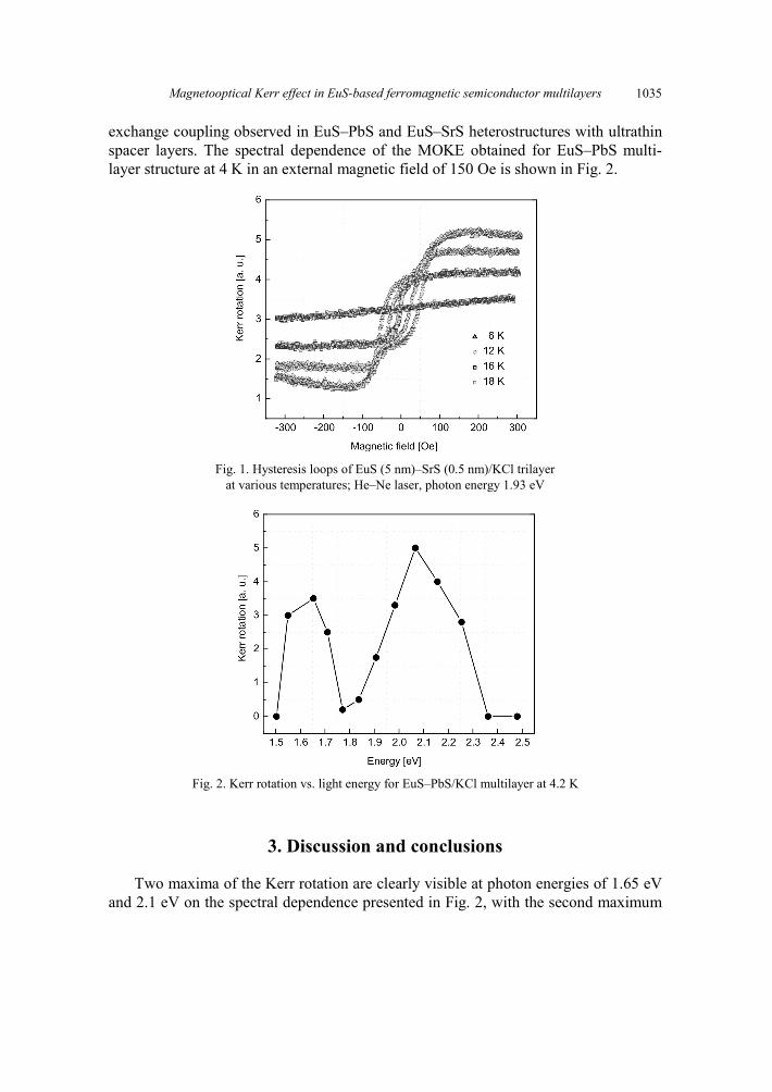
Magnetooptical Kerr effect in EuS-based ferromagnetic semiconductor multilayers 1035
exchange coupling observed in EuS–PbS and EuS–SrS heterostructures with ultrathin spacer layers. The spectral dependence of the MOKE obtained for EuS–PbS multi-layer structure at 4 K in an external magnetic field of 150 Oe is shown in Fig. 2.
Fig. 1. Hysteresis loops of EuS (5 nm)–SrS (0.5 nm)/KCl trilayer at various temperatures; He–Ne laser, photon energy 1.93 eV
Fig. 2. Kerr rotation vs. light energy for EuS–PbS/KCl multilayer at 4.2 K
3. Discussion and conclusions
Two maxima of the Kerr rotation are clearly visible at photon energies of 1.65 eV and 2.1 eV on the spectral dependence presented in Fig. 2, with the second maximum
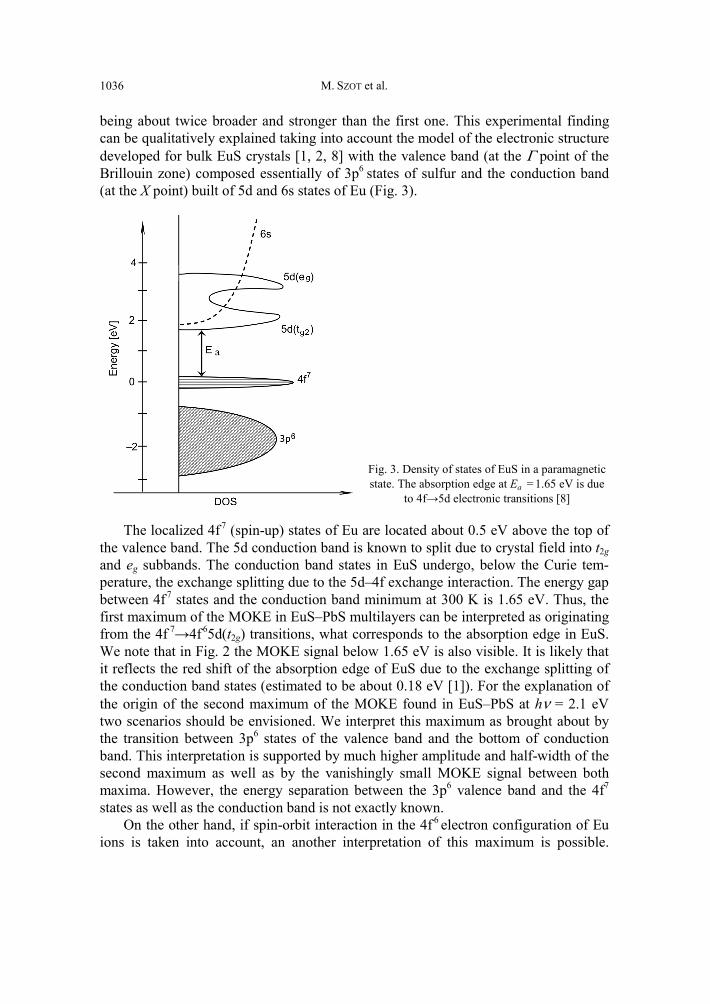
M. SZOT et al. 1036
being about twice broader and stronger than the first one. This experimental finding can be qualitatively explained taking into account the model of the electronic structure developed for bulk EuS crystals [1, 2, 8] with the valence band (at the Γ point of the Brillouin zone) composed essentially of 3p6 states of sulfur and the conduction band (at the X point) built of 5d and 6s states of Eu (Fig. 3).
Fig. 3. Density of states of EuS in a paramagnetic state. The absorption edge at Ea = 1.65 eV is due
to 4f→5d electronic transitions [8]
The localized 4f7 (spin-up) states of Eu are located about 0.5 eV above the top of the valence band. The 5d conduction band is known to split due to crystal field into t2g and eg subbands. The conduction band states in EuS undergo, below the Curie tem-perature, the exchange splitting due to the 5d–4f exchange interaction. The energy gap between 4f7 states and the conduction band minimum at 300 K is 1.65 eV. Thus, the first maximum of the MOKE in EuS–PbS multilayers can be interpreted as originating from the 4f 7→4f65d(t2g) transitions, what corresponds to the absorption edge in EuS. We note that in Fig. 2 the MOKE signal below 1.65 eV is also visible. It is likely that it reflects the red shift of the absorption edge of EuS due to the exchange splitting of the conduction band states (estimated to be about 0.18 eV [1]). For the explanation of the origin of the second maximum of the MOKE found in EuS–PbS at hν = 2.1 eV two scenarios should be envisioned. We interpret this maximum as brought about by the transition between 3p6 states of the valence band and the bottom of conduction band. This interpretation is supported by much higher amplitude and half-width of the second maximum as well as by the vanishingly small MOKE signal between both maxima. However, the energy separation between the 3p6 valence band and the 4f7 states as well as the conduction band is not exactly known.
On the other hand, if spin-orbit interaction in the 4f 6 electron configuration of Eu ions is taken into account, an another interpretation of this maximum is possible.
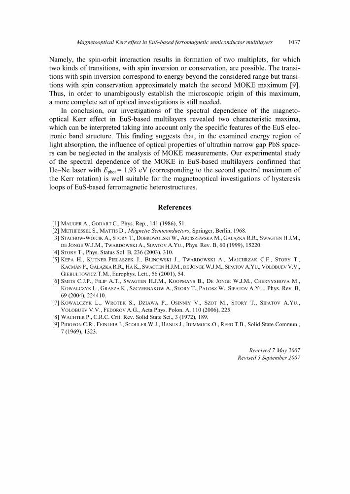
Magnetooptical Kerr effect in EuS-based ferromagnetic semiconductor multilayers 1037
Namely, the spin-orbit interaction results in formation of two multiplets, for which two kinds of transitions, with spin inversion or conservation, are possible. The transi-tions with spin inversion correspond to energy beyond the considered range but transi-tions with spin conservation approximately match the second MOKE maximum [9]. Thus, in order to unambigously establish the microscopic origin of this maximum, a more complete set of optical investigations is still needed.
In conclusion, our investigations of the spectral dependence of the magneto-optical Kerr effect in EuS-based multilayers revealed two characteristic maxima, which can be interpreted taking into account only the specific features of the EuS elec-tronic band structure. This finding suggests that, in the examined energy region of light absorption, the influence of optical properties of ultrathin narrow gap PbS space-rs can be neglected in the analysis of MOKE measurements. Our experimental study of the spectral dependence of the MOKE in EuS-based multilayers confirmed that He–Ne laser with Ephot = 1.93 eV (corresponding to the second spectral maximum of the Kerr rotation) is well suitable for the magnetooptical investigations of hysteresis loops of EuS-based ferromagnetic heterostructures.
References
[1] MAUGER A., GODART C., Phys. Rep., 141 (1986), 51. [2] METHFESSEL S., MATTIS D., Magnetic Semiconductors, Springer, Berlin, 1968. [3] STACHOW-WÓJCIK A., STORY T., DOBROWOLSKI W., ARCISZEWSKA M., GAŁĄZKA R.R., SWAGTEN H.J.M.,
DE JONGE W.J.M., TWARDOWSKI A., SIPATOV A.YU., Phys. Rev. B, 60 (1999), 15220. [4] STORY T., Phys. Status Sol. B, 236 (2003), 310. [5] KĘPA H., KUTNER-PIELASZEK J., BLINOWSKI J., TWARDOWSKI A., MAJCHRZAK C.F., STORY T.,
KACMAN P., GAŁĄZKA R.R., HA K., SWAGTEN H.J.M., DE JONGE W.J.M., SIPATOV A.YU., VOLOBUEV V.V., GIEBUŁTOWICZ T.M., Europhys. Lett., 56 (2001), 54.
[6] SMITS C.J.P., FILIP A.T., SWAGTEN H.J.M., KOOPMANS B., DE JONGE W.J.M., CHERNYSHOVA M., KOWALCZYK L., GRASZA K., SZCZERBAKOW A., STORY T., PALOSZ W., SIPATOV A.YU., Phys. Rev. B, 69 (2004), 224410.
[7] KOWALCZYK L., WROTEK S., DZIAWA P., OSINNIY V., SZOT M., STORY T., SIPATOV A.YU., VOLOBUEV V.V., FEDOROV A.G., Acta Phys. Polon. A, 110 (2006), 225.
[8] WACHTER P., C.R.C. Crit. Rev. Solid State Sci., 3 (1972), 189. [9] PIDGEON C.R., FEINLEIB J., SCOULER W.J., HANUS J., JDIMMOCK.O., REED T.B., Solid State Commun.,
7 (1969), 1323.
Received 7 May 2007 Revised 5 September 2007
Materials Science-Poland, Vol. 26, No. 4, 2008
Pseudodipolar model of surface magnetostriction for thin layers with roughness
T. SZUMIATA*, M. GZIK-SZUMIATA, K. BRZÓZKA
Department of Physics, Technical University of Radom, ul. Krasickiego 54, 26-600 Radom, Poland
An effective magnetostriction model for monocrystalline thin films of cubic structure has been pre-sented. The film roughness was simulated by cubicoidal steps on surface repeated in the plane with a constant period. In order to describe a magnetoelastic energy, a pseudodipolar spin–spin interaction was considered. Lattice summations of strain dependent energy contribution were performed symbolically. A significant difference of magnetoelastic energy compared with the film interior was observed only in the first atomic layer at the surface. An effective pseudodipolar magnetostriction constant λeff for rough film was determined by estimating the volume of surface region and considering the magnetostriction data for bulk material. Thickness dependence of λeff for bcc Fe film has been presented and compared with magnetic dipolar contribution.
Key words: magnetic thin layer; surface magnetostriction; surface roughness; pseudodipolar interactions
1. Introduction
A concept of surface magnetostriction is a natural consequence of Neel’s idea of surface magnetic anisotropy [1] evidenced experimentally by means of ferromagnetic resonance (FMR) [2]. The surface magnetostriction was observed for the first time in multilayers with strain modulated ferromagnetic resonance technique (SMFMR) [3]. Changes of the effective magnetostriction constants with film thickness were attri-buted to varying ratio of the number of surface atoms to the total population of atoms in the material. Theoretical predictions of dipolar and electronic contributions to the surface magnetostriction (within Draaisma–de Jonge [4] and Bruno models [5], re-spectively) have been reported in papers [6, 7]. Non-epitaxial growth of metallic films creates surface roughness which should be taken into account while considering expe-rimental magnetostriction data [8, 9]. We propose a simple theoretical model predict-ing the effective magnetostriction constant values of rough films based on the values for the bulk material.
__________
*Corresponding author, e-mail: [email protected]
T. SZUMIATA et al. 1040
2. Pseudodipolar interactions
We consider fully localized spins coupled via effective interaction represented by pseudodipolar term, which describes both anisotropic exchange energy and single-ion anisotropy one. [10]. Pseudodipolar Hamiltonian takes the form similar to that for magnetic dipolar interactions:
( )( ) ( , ) ( ) ( ) ( ) ( )A A
1| |3
i, j i j i j i jz zH J S S⎛ ⎞= ⋅ − ⋅⎜ ⎟
⎝ ⎠r S S (1)
( )izS and ( )j
zS are the components of spins i and j parallel to the line connecting these two spins; r(i,j) is the vector describing a relative position of spins, JA(|r(i,j)|) is an ex-change integral value at a distance |r(i,j)| ≡ r(i,j). In the case of single-ion magnetocrys-talline anisotropy S(i) ≡ S(j) and JA(|r(i,j)|) has a meaning of a radial function which de-scribes the strength of magnetocrystalline anisotropy for a given interatomic distance. Hamiltonian (1) can be written in a tensor-like form:
( , ) ( , )
( ) ( , ) ( , ) ( ) ( ) ( , )A A ( , ) 2
1( ) ;( ) 3
i j i ji, j i j i j i j i j k l
kl k l kl kli j
x xH J r G S S Gr
δ= = − (2)
and then can be transformed into a semi-classical notation:
( ) ( )
( ) ( , ) 2 ( , ) ( , ) 2 ( , ) ( ) ( )A A ( ) | | ( ) | |
| | | |
i ji, j i j i j i j i j i jk l
kl A kl k lS SH J r S G J r S GS S
α α= = (3)
where ( ) ( ), i jk lα α are the direction cosines of spins (i) and (j) and |S| is an effective
value of the spin. Thus, a contribution to the density of the second-order anisotropy energy could be expressed as
( , ) 2
( , ) ( , ) ( ) ( ) ( , ) ( , )AA
spin
1 ( ) | S |;2
i ji j i j i j i j i j
kl k l kl klJ ru A A G
Vα α= = (4)
where Vspin is a volume per one spin. The factor 1/2 has been applied in Eq. (4) to avoid double summation in further calculations of the total energy of the system. Since magnetoelastic energy results from a strain (εmn) dependence of anisotropy energy, its density may be described by means of the fourth-rank tensor ( , )i j
klmnB :
( , ) 2
( , ) ( , ) ( ) ( ) ( , ) ( , ) ( , )ME A
spin
1 | |;2
i ji j i j i j i j i j i jkl
klmn k l mn klmn klmn mn
A Su B B J r GV
α α εε ε
∂ ∂ ⎡ ⎤= = = ⎣ ⎦∂ ∂ (5)
Further recalculations allow one to express the tensor ( , )i jklmnB by two dimensionless
tensors J ( , )i jklmnb and P ( , )i j
klmnb :
Surface magnetostriction for thin layers with roughness 1041
2( , ) J ( , ) P ( , )
A A 0spin
( , ) ( , ) ( , )J ( , ) P ( , ) ( , )
NN0
1 | S | ;2
and
i j i j i jklmn klmn klmn
i j i j i ji j i j i jkl m n
klmn klmn klmn
B J b P a bV
G x xb b Gr aε
⎡ ⎤= +⎣ ⎦
∂= = ⋅∂
(6)
The parameters JA and J P stand for the value and the spatial derivative of the radi-al function JA(r(i,j)) in the distance of nearest neighbours rNN, respectively, when pseu-dodipolar interactions are limited to the first coordination zone (a0 is the lattice con-stant of cubic crystalline structure).
In order to obtain the total value of local density of magnetoelastic energy for ith spin site, lattice summations over index j have been performed analytically within the first coordination zone. Calculations have been made for the case of saturation (αk
(i) ≡ αk(j)).
The results show that only in the first atomic layer at the surface the magnetoelastic energy differs from that in the film interior. Regarding bcc films, the values of all components of dimensionless tensors J ( , )i j
klmnb and P ( , )i jklmnb in the surface layer are twice smaller than those in
the bulk region (whereas in the case of fcc structure such relations are more complex). This means that magnetostriction of bcc films is characterized by a magnetoelastic tensor of the cubic symmetry both in the interior and at the surface.
3. Effective magnetostriction
Minimization of magnetoelastic and elastic energies, described by means of mag-netoelastic tensor and elastic constants, respectively, leads to the calculation of magne-tostriction constant λ (for a given direction). This dimensionless quantity is a simple measure of relative strain induced by applying a saturation magnetic field. The results of calculations of the Bklmn tensor (presented in the previous section) give a very sim-ple relation between magnetostriction constants obtained for bulk material (λv) and flat surface region (λs) in the case of the bcc structure: λs = λv/2, both for [100] and [001] directions, i.e. in-plane and perpendicular to the plane, respectively.
In order to calculate the effective magnetostriction constant for a rough thin layer, it is necessary to estimate the fraction of atoms situated on the surface. The object of our investigations was a single magnetic film of a thickness t with surfaces in the form of cubicoidal steps of the depth σ and size ξ, repeated in the plane with the space pe-riod q (Fig. 1). Considering the volume of surface region (of the thickness h equal to a half of the lattice constant a0) an effective magnetostriction constant λeff of rough film could be expressed as follows:
( )eff v surf surf s v2
2 4; 1ht q
σξλ λ λ λ λ λ ⎛ ⎞= + = − +⎜ ⎟
⎝ ⎠ (7)
under the assumption: σ << t; λsurf is the surface magnetostriction constant (in [ppm⋅nm]) for a rough surface.
T. SZUMIATA et al. 1042
Fig. 1. Scheme of the film roughness model: a) projection from the top, b) a perspective view of the surface
Fig. 2. Dependence of the effective magnetostriction constant for ideal and rough films on the reciprocal film thickness: a) pseudodipolar model, b) magnetic dipolar contribution
Surface magnetostriction for thin layers with roughness 1043
In Figure 2a, a linear dependence of the effective magnetostriction constant (Eq. (7a)) on the reciprocal film thickness is shown for the case of the bcc Fe structure (λv = 24.1 ppm, h = a0/2 = 0.143 nm). We point to a significant reduction of magneto-striction for a small ξ size of steps (huge roughness area; negative value of the surface magnetostriction constant) in comparison to the case of flat surface (σ = 0).
The magnetic dipolar contribution to the in-plane magnetostriction constant of the bcc Fe film is shown in Fig. 2b. Appropriate calculations were based on models de-scribed in [6, 11, 12]. The surface roughness was represented by oblate ellipsoids (of semiaxes ξ = q/2 >> σ/2 ) in order to simplify the estimation of demagnetization ener-gy. In this case, the effective dipolar magnetostriction constant is given by:
( )2
eff v surf surf s v 0rdip dip dip dip dip dip dip
2 π;4
ht
σλ λ λ λ λ λ λξ
= + = − + (8)
where vdipλ = –1.91 ppm and s
dipλ = –4.93 ppm denote dipolar magnetostriction con-stants for internal and flat surface regions, respectively [12]. The magnetostriction constant 0r
dipλ = 15.1 ppm describes the influence of the magnitude of the roughness being defined as:
( )2
0r 0 sdip
11 12
π8 c
Mc
μλ =−
(9)
following the model developed in [11]. Ms is the saturation magnetization, μ0 – mag-netic permeability of the vacuum and c11, c12 – elastic constants. The dipolar contribu-tion to the magnetostriction of the Fe film interior is about 8% with respect to elec-tronic (pseudodipolar) one, whereas surface dipolar contribution is more significant – ca. 25%. Results presented in Fig. 2b show that roughness tends to compensate the dipolar surface magnetostriction.
4. Conclusions
Our model, based on pseudodipolar interactions of localized spins, relates the surface magnetostriction parameters of thin films to the magnetostriction constants of bulk material. We have shown that electronic contribution to the surface magne-tostriction of bcc Fe monocrystalline films increases with increasing surface roughness (fine steps of high surface density). It results in significant reduction of the effective magnetostriction in the case of very thin layers. We also have proven that magnetic dipolar contribution to the surface magnetostriction is not negligible. However, the surface roughness could partially compensate this contribution due to the opposite sign of surface magnetostriction constant for flat and rough parts of the surface, re-spectively. The energy of long range magnetic dipolar interactions depends both on
T. SZUMIATA et al. 1044
the volume of roughness region and the roughness shape. In a more advanced ap-proach, a continuous magnetized medium should be replaced by a discrete system of magnetic moments of atoms forming given structure. A summation of the energy of long range dipolar interactions should be performed over the whole structure what makes such procedure extremely time-consuming. Various directions of epitaxial growth of real films and their possible polycrystallinity as well as the influence of a kind of substrate seem to be essential questions in further development of our mag-netostriction model what will enable a reliable comparison with experimental data.
References
[1] NÉEL M.L., J. Phys. Radium, 15 (1954) 225. [2] GRADMANN U., J. Magn. Magn. Mater., 54–57 (1986), 733. [3] SZYMCZAK H., ŻUBEREK R., KRISHNAN R., YOUN K.B., SELLA C., IEEE Trans. Magn. MAG-23
(1987), 3699. [4] DRAAISMA H.J.G., DE JONGE W.J.M., J. Appl. Phys., 64 (1988), 3610. [5] BRUNO P., J. Phys. F: Met. Phys., 18 (1988), 1291. [6] SZUMIATA T., SZYMCZAK H., ŻUBEREK R., IEEE Trans. Magn., 29, (1993), 3132. [7] ŻUBEREK R., ŻYMIERSKA D. , SZYMCZAK H., Acta Phys. Polon. A, 85 (1994), 439. [8] KIM Y.K., SILVA T. J., Appl. Phys. Lett., 68 (1996), 2885. [9] HOLLINGWORTH M. P., GIBBS M. R. J., MURDOCH S. J., J. Appl. Phys., 94 (2003), 7235.
[10] DU TRÉMOLET DE LACHEISSERIE E., J. Magn. Magn. Mater, 67 (1987), 102. [11] SZYMCZAK H., REWIEŃSKI M., ŻUBEREK R., J. Magn. Magn. Mater, 139 (1995), 151. [12] SZUMIATA T., GEHRING G.A., COOKE M.D., ŻUBEREK R., J. Magn. Magn. Mater., 242–245 (2002),
1428.
Received 7 May 2007 Revised 6 October 2007
Materials Science-Poland, Vol. 26, No. 4, 2008
Raman spectroscopy of Zn1–xCoxO bulk mixed crystals
W. SZUSZKIEWICZ1*, J. F. MORHANGE2, M. SCHUMM3, M. LENTZE3, Z. GOŁACKI1, P. SKUPIŃSKI1, K. GRASZA1, J. GEURTS3
1Institute of Physics, Polish Academy of Sciences, al. Lotników 32/46, 02-668 Warsaw, Poland 2Institut des Nanosciences de Paris, Université Pierre et marie Curie,
CNRS UMR 7588, 140 rue de Lourmel, 75015 Paris, France 3Physikalisches Institut der Universität Würzburg, Am Hubland, 97074 Würzburg, Germany
We report on a study of structural properties of Zn1–xCoxO by micro- and macro-Raman scattering from phonons. Bulk mixed crystals (x ≤ 0.03), grown by chemical vapour transport were investigated between 5 K and 295 K. Beside the common eigenmodes of the ZnO host lattice, we observed disorder-induced lattice vibration modes and a structure, tentatively assigned to a local vibration mode of the Co impurity. Our results are compared with literature data of other ZnO-based diluted magnetic semiconduc-tors such as (Zn,Mn)O.
Key words: Zn1–xCoxO; Raman scattering; lattice vibrations; diluted magnetic semiconductor
1. Introduction and motivation
In recent years, diluted magnetic semiconductors (DMS) have attracted interest for their potential application in future spin-based electronics (spintronics) [1]. Among these materials, DMSs based on ZnO play a prominent role since room temperature ferromagnetism (RTFM) arising from carrier-mediated exchange interactions has been predicted for several transition metal doped ZnO (ZnO:TM) [2, 3]. One of these prom-ising materials is the mixed crystal Zn1–xCoxO.
Many studies on the magnetic properties of Zn1–xCoxO have been performed until now but their results were often ambiguous or even contradictory. The magnetic prop-erties of this material depend on the conditions during the crystal growth and also on the sample type (bulk crystal, thin layer, ceramic sample, nanocrystal, or nanowire) and on the after-growth treatment (e.g. annealing). In the case of polycrystalline bulk Zn1–xCoxO samples prepared by solid state reaction method, most of them exhibited __________
*Corresponding author, e-mail: [email protected]
W. SZUSZKIEWICZ et al. 1046
a paramagnetic or even antiferromagnetic behaviour at room temperature (RT). The RTFM observed in some other samples was attributed either to the generation of oxygen vacancies or the appearance of Co clusters. Similar explanations (or the formation of sec-ondary phases containing Co) were proposed for bulk polycrystalline ferromagnetic sam-ples prepared by other methods. Experimental reports of RTFM in selected Zn1–xCoxO films have further intensified the interest in this system. Nevertheless, in spite of numerous investigations, a general understanding of its magnetic properties is still missing.
There is a general agreement that a key question for the understanding of all these results is whether the material contains only randomly distributed TM ions at the sub-stitutional position in the host crystal lattice or if the material under interest contains also (mostly?) clusters, precipitates or secondary phases that are responsible for the observed magnetic properties [4–7].
One of the possible experimental methods to study the structure properties of ma-terials is Raman spectroscopy. Raman scattering studies on Zn1–xCoxO system started very recently, all forms of possible samples were analyzed (see, e.g., [8–13] and refer-ences therein). All but one ([10]) papers were limited to micro-Raman studies on sam-ples with composition varying from the Co content below x = 0.01 up to x = 0.20 in an extreme case. Most measurements were performed at RT only, without any polariza-tion analysis of the recorded spectra. The presence of such precipitates as Co (x = 0.05, [9]) and/or various cobalt oxides or cobalt spinel (x > 0.05, [11]) has been found (or at least suggested) for selected (not all) samples when the mixed crystal composition exceeds at least x = 0.03. Several local vibrational modes (LVMs) are expected for a transition metal impurity occupying a substitutional site in the hexago-nal crystal lattice (see, e.g., [14, 15]). However, in spite of numerous experimental efforts, expected sharp structures, resulting from the LVMs of Co, have not been ob-served in the Raman spectra until now.
The goal of the present work is to get information about the position of the Co ions in the ZnO crystal lattice and about the overall crystal structure by analysing the lattice dynamics. Raman spectroscopy and bulk Zn1–xCoxO samples corresponding to x ≤ 0.03 have been selected for this purpose.
2. Experimental
For the growth of the Zn1–xCoxO crystals, the chemical vapour transport (CVT) method was applied. The crystals were grown at about 1050–1100 °C in Zn-rich con-ditions. Both inert (Ar, N2) and reactive (Br, Cl) gases supporting the transport of dopants were used in the growth system. Pure ZnO crystals were grown both in Zn-rich and stoichiometric conditions, part of them was annealed in oxygen after the growth. More details can be found, e.g., in [10].
Due to a similarity of the atomic masses of Co and Zn one cannot expect a signifi-cant evolution of the parameters describing phonon modes with changing mixed crys-tal composition, at least for the very narrow composition range analyzed in this paper.
Raman spectroscopy of Zn1–xCoxO bulk mixed crystals 1047
Under these circumstances, only two types of samples have been considered: slightly Co-doped ZnO crystals (with x well below 0.01) and real mixed crystals, nominally containing a few percent of Co (but corresponding to the composition for which pos-sible presence of neither pure Co nor cobalt spinel has been reported). Pure ZnO crys-tals were also grown for a comparison. The structure quality of the selected crystals grown by the method described was previously checked by the X-ray diffraction (not reported here), a possible presence of other phases was not detected by this method.
Typical Raman scattering measurements were performed using a Jobin–Yvon U1000 double monochromator in the spectral range from 300 cm–1 to 650 cm–1 with the spectral resolution close to 1 cm–1. The Ar+ laser lines of the wavelengths 514.5 nm or 476.5 nm were applied for the excitation. A Peltier effect cooled photon count-ing system and S20 photomultiplier served as the detector system. For the low-temperature measurements, the sample was placed on the cold finger of a continuous-flow helium cryostat, the sample temperature was estimated to be about 15 K. Because the bulk samples were polycrystalline or not oriented, no polarization analysis of the Raman scattering has been performed.
The micro-Raman measurements with the use of the microscope were performed on selected samples both at RT and at 5 K. The 514.5 nm Ar+ laser line was applied for the excitation. The light was focused on the sample surface by a 80× ULWD microscope ob-jective, the scattered light was analysed by a triple monochromator (Dilor XY, focal length 500 mm), and accumulated with a liquid-nitrogen cooled CCD-array detector.
3. Results and discussion
Figure 1 shows the Raman spectra taken at RT with two experimental set-ups on pure ZnO and two Co-doped ZnO samples with a low Co content. The upper panel and the lower panel show the macro-Raman spectra, the micro-Raman data are shown in the middle. A non-oriented sample has been used for these measurements hence the relative intensities of the principal peaks are slightly different. The band near 335 cm–1
can be interpreted as a double phonon corresponding to the subtractive combination of the E2 (high) mode at 438 cm–1 and the E2 (low) mode at 100 cm–1.The three structures observed in the middle correspond to typical and well known first order host lattice modes, namely to A1 (TO) 378 cm–1, E1 (TO) 410 cm–1, and E2 (high) 438 cm–1, respec-tively. The numerical values of frequencies given above are typical ones but can vary, as the frequencies of various extraordinary phonons change with the orientation in an uniaxial material. The mode with the maximum at about 539 cm–1 is only observed in Co doped ZnO, and can thus been interpreted as an impurity mode or at least a dis-order induced one. The presence of additional modes (or band) in the spectral region between 500 cm–1 and 600 cm–1 was reported previously not only for Zn1–xCoxO, but also for ZnO containing other dopants, like Mn (see, e.g., [10, 16]) or Ti [16]. On the other hand, modes in this spectral range are not clearly observed on Zn1–xCoxO films with a high Co content [13] or on Co-doped ZnO nanowires [12]. The presence of the
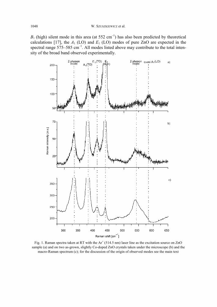
W. SZUSZKIEWICZ et al. 1048
B1 (high) silent mode in this area (at 552 cm–1) has also been predicted by theoretical calculations [17], the A1 (LO) and E1 (LO) modes of pure ZnO are expected in the spectral range 575–585 cm–1. All modes listed above may contribute to the total inten-sity of the broad band observed experimentally.
Fig. 1. Raman spectra taken at RT with the Ar+ (514.5 nm) laser line as the excitation source on ZnO
sample (a) and on two as-grown, slightly Co-doped ZnO crystals taken under the microscope (b) and the macro-Raman spectrum (c); for the discussion of the origin of observed modes see the main text
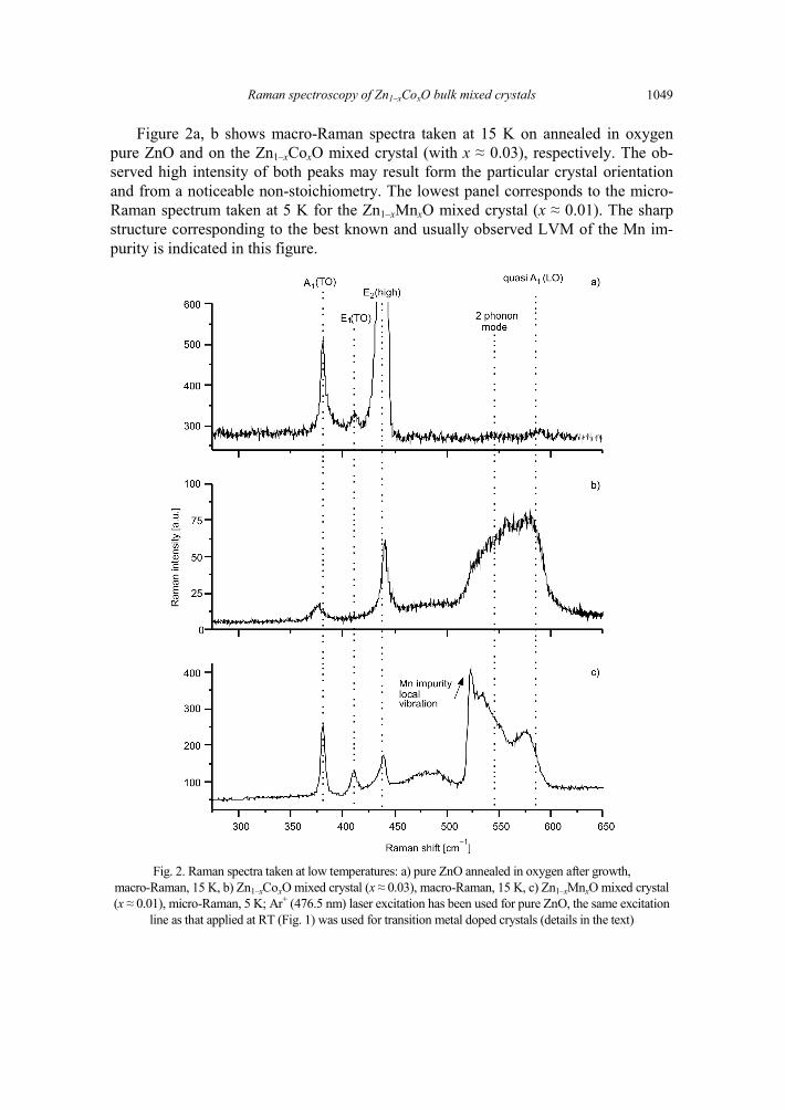
Raman spectroscopy of Zn1–xCoxO bulk mixed crystals 1049
Figure 2a, b shows macro-Raman spectra taken at 15 K on annealed in oxygen pure ZnO and on the Zn1–xCoxO mixed crystal (with x ≈ 0.03), respectively. The ob-served high intensity of both peaks may result form the particular crystal orientation and from a noticeable non-stoichiometry. The lowest panel corresponds to the micro-Raman spectrum taken at 5 K for the Zn1–xMnxO mixed crystal (x ≈ 0.01). The sharp structure corresponding to the best known and usually observed LVM of the Mn im-purity is indicated in this figure.
Fig. 2. Raman spectra taken at low temperatures: a) pure ZnO annealed in oxygen after growth, macro-Raman, 15 K, b) Zn1–xCoxO mixed crystal (x ≈ 0.03), macro-Raman, 15 K, c) Zn1–xMnxO mixed crystal (x ≈ 0.01), micro-Raman, 5 K; Ar+ (476.5 nm) laser excitation has been used for pure ZnO, the same excitation
line as that applied at RT (Fig. 1) was used for transition metal doped crystals (details in the text)
W. SZUSZKIEWICZ et al. 1050
The additional structure observed at 333 cm–1 is due to the second order Raman scattering. The intensity of this structure may be enhanced due to the crystal disorder. Some differences in the host lattice modes intensity ratio and the disappearance of the E1 (TO) mode results from different crystal orientations, as well as their slight fre-quency shift which is probably due to the “extraordinary” nature of some phonons in a uniaxial material as noted above. Some differences in the form of the broad bands in the spectral range between 500 cm–1 and 600 cm–1, presented in Fig. 1 and Fig. 2, may be observed. A similar modification of the form of this band with an increasing Co content in the mixed crystal can be found in some literature data concerning this system.
It should be stressed that, while in the case of Zn1–xMnxO mixed crystals several research groups observed and identified LVMs of Mn (or Mn-related complex) in ZnO and for one of these modes a really sharp structure has been observed at low tempera-tures (see, e.g., [10, 16] and Fig. 2) a similar vibration with well determined frequency is not observed for Zn1–xCoxO. Some additional small structures observed in the spec-tral range of interest can always be interpreted in another manner. The only exception could be a not very well pronounced structure at about 556 cm–1 at low temperatures on the samples containing a few percent of Co. This structure does not appear neither in pure ZnO nor in Zn1–xMnxO mixed crystals. Moreover, the form of the band ob-served on the Zn1–xCoxO samples cannot be explained by a selected, high-frequency host lattice modes and some combinations of other lattice modes resulting form the ZnO lattice vibrations only.
Several authors analyzing magnetic properties of ZnO-based DMS point to a dif-ference between doping with Mn and Co (e.g., [18]) and stress a sensitivity of a given DMS magnetic behaviour to the transition ion neighbourhood in the crystal lattice. Up to our knowledge, a detailed analysis of the local symmetry of Co2+ ions is possible only for a low composition range [19] where possible sharp local impurity vibrations cannot be observed. We believe that a proper explanation of the observed Raman spectra (both our and the literature data) could be the following. With an increasing Co content in Zn1–xCoxO, isolated Co2+ ions in the mixed crystal are replaced by a com-plex (containing, e.g., another Co2+ ion, an oxygen vacancy, a zinc interstitial, or a hydrogen ion) leading to a local deformation of the lattice. In particular, according to the literature, the Co-related complex may be not as simple as that corresponding to Mn dopant in ZnO. Due to different possible orientations of such complexes and be-cause of interactions between the ions, one could expect a broadening of the local vibration mode and observe a rather broad band instead of finite frequencies for such excitations. Under these circumstances, the observed form of the vibration band could be considered as an optical evidence of a complex containing the Co2+ ion.
One should mention that mostly as-grown Zn1–xCoxO samples were investigated in the present paper. As is well known, post-growth annealing may modify the mixed crystal stoichiometry, type and density of defects, possible precipitates etc. The possi-ble influence of oxygen vacancies and Zn interstitials on the Raman spectrum has been mentioned in a few papers but more systematic studies of this kind are clearly re-
Raman spectroscopy of Zn1–xCoxO bulk mixed crystals 1051
quired. Results of such investigations should finally explain the origin of the variety of observed properties of different Zn1–xCoxO samples with nominally similar chemical compositions.
4. Conclusions
So far, experimental reports on ferromagnetism in Zn1–xCoxO have been contro-versial and seem to be sensitive to sample preparation and to post-growth treatment (like, e.g., annealing). It is very probable that precipitates of other Co-related crystal phases or clustering of the magnetic ions into an impurity phase might be responsible for such features. In spite of these controversies, Zn1–xCoxO is believed to be the best candidate for room temperature ferromagnetism among the TM-doped ZnO family. The present Raman spectra taken at frequencies above 300 cm–1 on bulk mixed crys-tals (containing not more than 1% and a few percent of Co, respectively) do not indi-cate a possible presence of additional crystal phases. However, the analysis of Raman scattering spectra suggests that they cannot be simply due to the presence of this ele-ment at the substitutional site of the cation sublattice. It is very probable that a re-placement of Zn by Co ion is accompanied by a local lattice distortion and/or the crea-tion of a complex defect. Various complexes (containing, e.g., another cobalt ion, a zinc atom at the interstitial position, oxygen vacancy, or a hydrogen atom) have been previously proposed. The suggested interpretation of Raman scattering spectra is confirmed by a difference seen in the comparison of the presented results with the literature data, corresponding to Zn1–xMnxO. In the latter case, a few LVMs (and among them at least one really “sharp” with a well defined frequency) have been ob-served in the lattice dynamics by a few research groups. More experimental data (in particular, taken on annealed and as-grown samples in a lower frequency region) are clearly required in order to get more information about the nature of complexes, in-volved in the creation of room temperature ferromagnetism.
Acknowledgements
The present work has been supported in part by a Polish research grants Nos. 3 T08A 05128 and N515 015 32/0997 and by the Polonium project 7011/R07/R08.
References
[1] WOLF S.A., AWSCHALOM D.D., BUHRMAN R.A., DAUGHTON J.M., VON MOLNÁR S., ROUKES M.L., CHTCHELKANOVA A.Y., TREGER D.M., Science, 294 (2001), 1488.
[2] DIETL T., OHNO H., MATSUKURA F., CIBERT J., FERRAND D., Science, 287 (2000), 1019. [3] SATO K., KATAYAMA-YOSHIDA H., Physica E, 10 (2001), 251. [4] PEARTON S.J., NORTON D.P., IP K., HEO Y.W., STEINER T., Prog. Mater. Sci., 50 (2005), 293. [5] LIU C., YUN F., MORKOC H., J. Mater. Sci.: Mater. Electr., 16 (2005), 555. [6] SESHADRI R., Current Opinion in Solid State Mater. Sci., 9 (2005), 1.
W. SZUSZKIEWICZ et al. 1052
[7] OZGUR U., ALIVOV Y.I., LIU C., TEKE A., RESHCHIKOV M.A., DOĞAN S., AVRUTIN V., CHO S.-J., MORKOÇ H., J. Appl. Phys. 98 (2005), 041301.
[8] HASUIKE N., FUKUMURA H., HARIMA H., KISODA K., MATSUI H., SAEKI H., TABATA H., J. Phys.: Condens. Mater, 16 (2004) S5807.
[9] MILLOT M., GONZALEZ J., MOLINA I., SALAS B., GOLACKI Z., BROTO J.M., RAKOTO H., GOIRAN M., J. Alloys Compds., 423 (2006), 224.
[10] JOUANNE M., MORHANGE J.F., SZUSZKIEWICZ W., GOŁACKI Z, MYCIELSKI A., Phys. Stat. Sol. C, 3 (2006), 1205.
[11] SAMANTA K., BHATTACHARYA P., KATIYAR R.S., IWAMOTO W., PAGLIUSO P.G., RETTORI C., Phys. Rev. B, 73 (2006), 245213.
[12] CUI J., GIBSON U., Phys. Rev. B, 74 (2006), 045416. [13] ZHOU H., CHEN L., MALIK V., KNIES C., HOFMANN D.M., BHATTI K.P., CHAUDHARY S., KLAR P.J.,
HEIMBRODT W., KLINGSHIRN C., KALT H., Phys. Stat. Sol. A, 204 (2007), 112. [14] THURIAN P., KACZMARCZYK G., SIEGLE H., HERTZ R., HOFFMANN A., BROSER I., MEYER B.K.,
HOFFBAUER R., SCHERZ U., Mater. Sci. Forum, 196–201 (1995), 1571. [15] SCHREPEL C., GÖBEL C., SCHERZ U., THURIAN P., KACZMARCZYK G., HOFFMANN A., Z. Physik.
Chem., 201 (1997), 21. [16] GEBICKI W., OSUCH K., JASTRZEBSKI C., GOLACKI Z, GODLEWSKI M., Superlatt. Microstr. 38 (2005), 428. [17] MANJON F.J., MARI B., SERRANO J, ROMERO A.H., J. Appl. Phys., 97 (2005), 053516. [18] KITTILSTVED K.R., GAMELIN D.R., J. Appl. Phys., 99 (2006), 08M112. [19] SATI P., HAYN R., KUZIAN R., REGNIER S., SCHÄFER S., STEPANOV A., MORHAIN C., DEPARIS C.,
LAÜGT M., GOIRAN M, GOLACKI Z., Phys. Rev. Lett., 96 (2006), 017203.
Received 7 May 2007 Revised 18 September 2007
Materials Science-Poland, Vol. 26, No. 4, 2008
Raman scattering studies of MBE-grown ZnTe nanowires
W. SZUSZKIEWICZ1*, J. F. MORHANGE2, E. DYNOWSKA1, E. JANIK1, W.H ZALESZCZYK1, A. PRESZ3, J. Z. DOMAGAŁA1, W. CALIEBE4, G. KARCZEWSKI1, T. WOJTOWICZ1
1Institute of Physics, Polish Academy of Sciences, Al. Lotników 32/46, 02-668 Warsaw, Poland 2Institut des Nanosciences de Paris, Université Pierre et marie Curie,
CNRS UMR 7588, 140 rue de Lourmel, 75015 Paris, France 3Institute of High Pressure Physics, PAS, ul. Sokołowska 29/37, 01-142 Warsaw, Poland
4Hasylab at DESY, Notkestr. 85, D-22603 Hamburg, Germany
We report on the first studies of the optical properties of MBE-grown ZnTe nanowires (NWs). The growth of ZnTe NWs was based on the Au-catalyzed vapour–liquid–solid mechanism and was performed on (001), (011), or (111)B-oriented GaAs substrates. Investigated NWs have a zinc-blende structure, the average diameter of about 30 nm, and typical length between 1 and 2 μm. Their growth axes are oriented along <111>-type directions of the substrate. The structural characterization of the NWs was performed by means of X-ray diffraction, using the synchrotron radiation corresponding to the wavelength of CuKα1 radiation W1 beamline at Hasylab DESY). The macro-Raman spectra of either as-grown NWs on GaAs substrate or of NWs removed from substrate and deposited onto Si were collected at temperatures from 15 K to 295 K using Ar+ and Kr+ laser lines. Strong enhancement of ZnTe-related LO-phonon structure was found for an excitation close to the exciton energy. Our studies revealed also the presence of small trigonal Te precipitates, typical of tellurium compounds.
Key words: ZnTe nanowire; Raman scattering; MBE growth; lattice dynamics
1. Introduction
The II–VI one-dimensional nanostructures such as ZnO, ZnS, ZnSe, or ZnTe nanowires (NWs) have attracted a lot of attention during the last few years due to their unique properties and potential applications in electronics and optoelectronics. Most available experimental data concern ZnO and papers devoted to metal chalcogenides are not very numerous. In particular, the crystal growth and properties of NWs made from telluride compounds seem to be restricted to some reports on ZnTe NWs ob-tained by various methods [1–8], on CdTe NWs [9–11], and on HgTe NWs [12]. __________
*Corresponding author, e-mail: [email protected]
W. SZUSZKIEWICZ et al. 1054
MBE growth of ZnTe NWs using the vapour–liquid–solid (VLS) method has been reported previously by some of the present authors [5]. The MBE technique offers some advantages in comparison to the alternative growth methods (e.g., chemical va-pour deposition or precipitation from solutions). In particular, the future fabrication of more complex NWs structures made of heterojunctions or multinary compounds should be easier because of the versatility of the MBE technique.
Raman scattering is a powerful tool for characterizing the structural properties of semiconductors. However, among the above mentioned papers describing the growth and properties of ZnTe NWs only one is devoted in part to this experimental technique [3]. The Raman spectroscopy is not very often applied also for investigations of other NW systems because of possible large intensity of luminescence in the spectral range close to the frequencies of interest. In the case of II–VI based NWs, Raman spectra have been accumulated on CdTe [9,10], CdSe [13], CdS [14], ZnSe [15,16], ZnS [17–19], several papers concern also ZnO pure or transition metal doped.
It should be stressed that in a typical case Raman scattering study on NWs is lim-ited to the Raman spectrum taken at room temperature (RT) on as-grown sample (usu-ally, NWs are not separated form the substrate after the catalytic growth). Only one example of the Raman studies on II–VI based NWs removed form the substrate and another one reporting on low temperature studies can be found in the literature for semiconductor systems mentioned above ([14] and [10], respectively).
The goal of the present work was to study the structural properties of MBE-grown ZnTe NWs by means of Raman scattering investigating both as-grown NWs and NWs separated from the substrate.
2. Experimental
ZnTe NWs were grown in an EPI 620 MBE system equipped with the low tempera-ture effusion cells and reflection high-energy electron diffraction (RHEED). The growth was performed from elemental Zn and Te sources on (001), (011), and (111)B-oriented, semi-insulating GaAs substrates. The growth process was based on the Au-catalyzed vapour–liquid–solid mechanism. The thin gold layer (from 3 Å to 20 Å thick) an-nealed in high vacuum prior to the NWs growth was applied as a source of catalytic nanoparticles. ZnTe NWs with an average diameter of about 30 nm and the typical length 1–2 μm were grown by this method. More details about the applied technology may be found in [5]. Several pictures have been taken after the growth with a scanning electron microscope (FE-SEM Leo 540).
The standard structural characterization of NWs was performed using synchrotron radiation at the W1.1 beamline at Hasylab (DESY) in Hamburg. The monochromatic X-ray beam of the wavelength λ = 1.54056 Å (corresponding to CuKα1 radiation) was selected for such a purpose. Two modes of measurements were applied, namely sym-metrical ω–2θ scan and coplanar 2θ scan in the glancing incidence geometry. These measurements allowed one to separate the contributions due to the polycrystalline
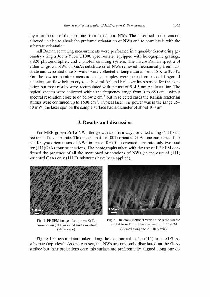
Raman scattering studies of MBE-grown ZnTe nanowires 1055
layer on the top of the substrate from that due to NWs. The described measurements allowed us also to check the preferred orientation of NWs and to correlate it with the substrate orientation.
All Raman scattering measurements were performed in a quasi-backscattering ge-ometry using a Jobin-Yvon U1000 spectrometer equipped with holographic gratings, a S20 photomultiplier, and a photon counting system. The macro-Raman spectra of either as-grown NWs on GaAs substrate or of NWs removed mechanically from sub-strate and deposited onto Si wafer were collected at temperatures from 15 K to 295 K. For the low-temperature measurements, samples were placed on a cold finger of a continuous flow helium cryostat. Several Ar+ and Kr+ laser lines served for the exci-tation but most results were accumulated with the use of 514.5 nm Ar+ laser line. The typical spectra were collected within the frequency range from 0 to 650 cm–1 with a spectral resolution close to or below 2 cm–1 but in selected cases the Raman scattering studies were continued up to 1500 cm–1. Typical laser line power was in the range 25–50 mW, the laser spot on the sample surface had a diameter of about 100 μm.
3. Results and discussion
For MBE-grown ZnTe NWs the growth axis is always oriented along <111> di-rections of the substrate. This means that for (001)-oriented GaAs one can expect four <111>-type orientations of NWs in space, for (011)-oriented substrate only two, and for (111)GaAs four orientations. The photographs taken with the use of FE SEM con-firmed the presence of all the mentioned orientations of NWs (in the case of (111) -oriented GaAs only (111)B substrates have been applied).
Fig. 1. FE SEM image of as-grown ZnTe nanowires on (011) oriented GaAs substrate
(plane view)
Fig. 2. The cross sectional view of the same sample as that from Fig. 1 taken by means of FE SEM
(viewed along the 1 10< > axis)
Figure 1 shows a picture taken along the axis normal to the (011) oriented GaAs substrate (top view). As one can see, the NWs are randomly distributed on the GaAs surface but their projections onto this surface are preferentially aligned along one di-
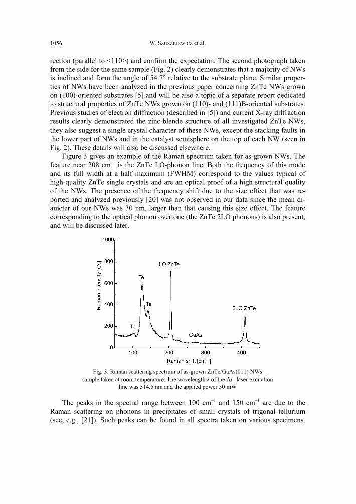
W. SZUSZKIEWICZ et al. 1056
rection (parallel to <110>) and confirm the expectation. The second photograph taken from the side for the same sample (Fig. 2) clearly demonstrates that a majority of NWs is inclined and form the angle of 54.7° relative to the substrate plane. Similar proper-ties of NWs have been analyzed in the previous paper concerning ZnTe NWs grown on (100)-oriented substrates [5] and will be also a topic of a separate report dedicated to structural properties of ZnTe NWs grown on (110)- and (111)B-oriented substrates. Previous studies of electron diffraction (described in [5]) and current X-ray diffraction results clearly demonstrated the zinc-blende structure of all investigated ZnTe NWs, they also suggest a single crystal character of these NWs, except the stacking faults in the lower part of NWs and in the catalyst semisphere on the top of each NW (seen in Fig. 2). These details will also be discussed elsewhere.
Figure 3 gives an example of the Raman spectrum taken for as-grown NWs. The feature near 208 cm–1 is the ZnTe LO-phonon line. Both the frequency of this mode and its full width at a half maximum (FWHM) correspond to the values typical of high-quality ZnTe single crystals and are an optical proof of a high structural quality of the NWs. The presence of the frequency shift due to the size effect that was re-ported and analyzed previously [20] was not observed in our data since the mean di-ameter of our NWs was 30 nm, larger than that causing this size effect. The feature corresponding to the optical phonon overtone (the ZnTe 2LO phonons) is also present, and will be discussed later.
Fig. 3. Raman scattering spectrum of as-grown ZnTe/GaAs(011) NWs
sample taken at room temperature. The wavelength λ of the Ar+ laser excitation line was 514.5 nm and the applied power 50 mW
The peaks in the spectral range between 100 cm–1 and 150 cm–1 are due to the Raman scattering on phonons in precipitates of small crystals of trigonal tellurium (see, e.g., [21]). Such peaks can be found in all spectra taken on various specimens.
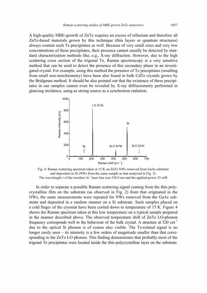
Raman scattering studies of MBE-grown ZnTe nanowires 1057
A high-quality MBE-growth of ZnTe requires an excess of tellurium and therefore all ZnTe-based materials grown by this technique (thin layers or quantum structures) always contain such Te precipitates as well. Because of very small sizes and very low concentrations of these precipitates, their presence cannot usually be detected by stan-dard characterization methods like, e.g., X-ray diffraction. However, due to the high scattering cross section of the trigonal Te, Raman spectroscopy is a very sensitive method that can be used to detect the presence of this secondary phase in an investi-gated crystal. For example, using this method the presence of Te precipitates (resulting from small non-stoichiometry) have been also found in bulk CdTe crystals grown by the Bridgman method. It should be also pointed out that the existence of these precipi-tates in our samples cannot even be revealed by X-ray diffractometry performed in glancing incidence, using as strong source as a synchrotron radiation.
Fig. 4. Raman scattering spectrum taken at 15 K on ZnTe NWs removed from GaAs substrate
and deposited on Si (NWs from the same sample as that analyzed in Fig. 3). The wavelength λ of the incident Ar+ laser line was 530.9 nm and the applied power 25 mW
In order to separate a possible Raman scattering signal coming from the thin poly-crystalline film on the substrate (as observed in Fig. 2) from that originated in the NWs, the same measurements were repeated for NWs removed from the GaAs sub-strate and deposited in a random manner on a Si substrate. Such samples placed on a cold finger of the cryostat have been cooled down to temperature of 15 K. Figure 4 shows the Raman spectrum taken at this low temperature on a typical sample prepared in the manner described above. The observed temperature shift of ZnTe LO-phonon frequency corresponds well to the behaviour of the bulk crystal. A structure at 520 cm–1 due to the optical Si phonon is of course also visible. The Te-related signal is no longer easily seen – its intensity is a few orders of magnitude smaller than that corre-sponding to the ZnTe LO phonon. This finding demonstrates that probably most of the trigonal Te precipitates were located inside the thin polycrystalline layer on the substrate.
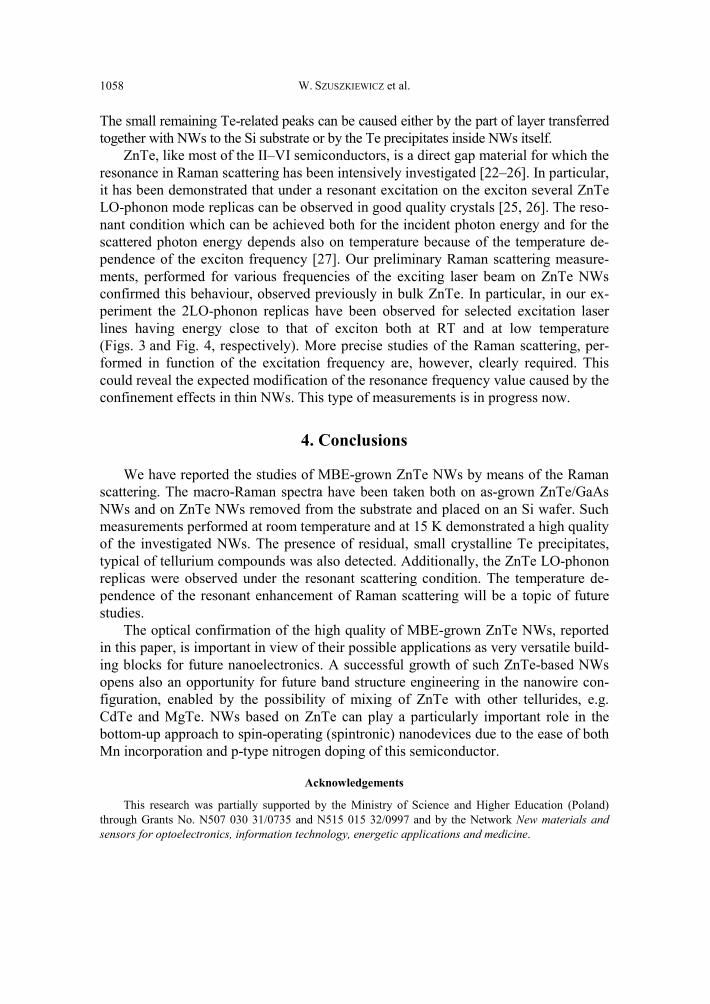
W. SZUSZKIEWICZ et al. 1058
The small remaining Te-related peaks can be caused either by the part of layer transferred together with NWs to the Si substrate or by the Te precipitates inside NWs itself.
ZnTe, like most of the II–VI semiconductors, is a direct gap material for which the resonance in Raman scattering has been intensively investigated [22–26]. In particular, it has been demonstrated that under a resonant excitation on the exciton several ZnTe LO-phonon mode replicas can be observed in good quality crystals [25, 26]. The reso-nant condition which can be achieved both for the incident photon energy and for the scattered photon energy depends also on temperature because of the temperature de-pendence of the exciton frequency [27]. Our preliminary Raman scattering measure-ments, performed for various frequencies of the exciting laser beam on ZnTe NWs confirmed this behaviour, observed previously in bulk ZnTe. In particular, in our ex-periment the 2LO-phonon replicas have been observed for selected excitation laser lines having energy close to that of exciton both at RT and at low temperature (Figs. 3 and Fig. 4, respectively). More precise studies of the Raman scattering, per-formed in function of the excitation frequency are, however, clearly required. This could reveal the expected modification of the resonance frequency value caused by the confinement effects in thin NWs. This type of measurements is in progress now.
4. Conclusions
We have reported the studies of MBE-grown ZnTe NWs by means of the Raman scattering. The macro-Raman spectra have been taken both on as-grown ZnTe/GaAs NWs and on ZnTe NWs removed from the substrate and placed on an Si wafer. Such measurements performed at room temperature and at 15 K demonstrated a high quality of the investigated NWs. The presence of residual, small crystalline Te precipitates, typical of tellurium compounds was also detected. Additionally, the ZnTe LO-phonon replicas were observed under the resonant scattering condition. The temperature de-pendence of the resonant enhancement of Raman scattering will be a topic of future studies.
The optical confirmation of the high quality of MBE-grown ZnTe NWs, reported in this paper, is important in view of their possible applications as very versatile build-ing blocks for future nanoelectronics. A successful growth of such ZnTe-based NWs opens also an opportunity for future band structure engineering in the nanowire con-figuration, enabled by the possibility of mixing of ZnTe with other tellurides, e.g. CdTe and MgTe. NWs based on ZnTe can play a particularly important role in the bottom-up approach to spin-operating (spintronic) nanodevices due to the ease of both Mn incorporation and p-type nitrogen doping of this semiconductor.
Acknowledgements
This research was partially supported by the Ministry of Science and Higher Education (Poland) through Grants No. N507 030 31/0735 and N515 015 32/0997 and by the Network New materials and sensors for optoelectronics, information technology, energetic applications and medicine.
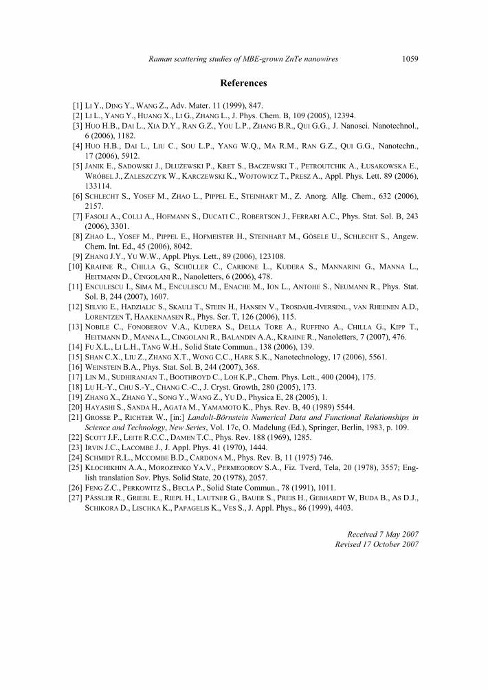
Raman scattering studies of MBE-grown ZnTe nanowires 1059
References
[1] LI Y., DING Y., WANG Z., Adv. Mater. 11 (1999), 847. [2] LI L., YANG Y., HUANG X., LI G., ZHANG L., J. Phys. Chem. B, 109 (2005), 12394. [3] HUO H.B., DAI L., XIA D.Y., RAN G.Z., YOU L.P., ZHANG B.R., QUI G.G., J. Nanosci. Nanotechnol.,
6 (2006), 1182. [4] HUO H.B., DAI L., LIU C., SOU L.P., YANG W.Q., MA R.M., RAN G.Z., QUI G.G., Nanotechn.,
17 (2006), 5912. [5] JANIK E., SADOWSKI J., DŁUŻEWSKI P., KRET S., BACZEWSKI T., PETROUTCHIK A., ŁUSAKOWSKA E.,
WRÓBEL J., ZALESZCZYK W., KARCZEWSKI K., WOJTOWICZ T., PRESZ A., Appl. Phys. Lett. 89 (2006), 133114.
[6] SCHLECHT S., YOSEF M., ZHAO L., PIPPEL E., STEINHART M., Z. Anorg. Allg. Chem., 632 (2006), 2157.
[7] FASOLI A., COLLI A., HOFMANN S., DUCATI C., ROBERTSON J., FERRARI A.C., Phys. Stat. Sol. B, 243 (2006), 3301.
[8] ZHAO L., YOSEF M., PIPPEL E., HOFMEISTER H., STEINHART M., GÖSELE U., SCHLECHT S., Angew. Chem. Int. Ed., 45 (2006), 8042.
[9] ZHANG J.Y., YU W.W., Appl. Phys. Lett., 89 (2006), 123108. [10] KRAHNE R., CHILLA G., SCHÜLLER C., CARBONE L., KUDERA S., MANNARINI G., MANNA L.,
HEITMANN D., CINGOLANI R., Nanoletters, 6 (2006), 478. [11] ENCULESCU I., SIMA M., ENCULESCU M., ENACHE M., ION L., ANTOHE S., NEUMANN R., Phys. Stat.
Sol. B, 244 (2007), 1607. [12] SELVIG E., HADZIALIC S., SKAULI T., STEEN H., HANSEN V., TROSDAHL-IVERSENL., VAN RHEENEN A.D.,
LORENTZEN T, HAAKENAASEN R., Phys. Scr. T, 126 (2006), 115. [13] NOBILE C., FONOBEROV V.A., KUDERA S., DELLA TORE A., RUFFINO A., CHILLA G., KIPP T.,
HEITMANN D., MANNA L., CINGOLANI R., BALANDIN A.A., KRAHNE R., Nanoletters, 7 (2007), 476. [14] FU X.L., LI L.H., TANG W.H., Solid State Commun., 138 (2006), 139. [15] SHAN C.X., LIU Z., ZHANG X.T., WONG C.C., HARK S.K., Nanotechnology, 17 (2006), 5561. [16] WEINSTEIN B.A., Phys. Stat. Sol. B, 244 (2007), 368. [17] LIN M., SUDHIRANJAN T., BOOTHROYD C., LOH K.P., Chem. Phys. Lett., 400 (2004), 175. [18] LU H.-Y., CHU S.-Y., CHANG C.-C., J. Cryst. Growth, 280 (2005), 173. [19] ZHANG X., ZHANG Y., SONG Y., WANG Z., YU D., Physica E, 28 (2005), 1. [20] HAYASHI S., SANDA H., AGATA M., YAMAMOTO K., Phys. Rev. B, 40 (1989) 5544. [21] GROSSE P., RICHTER W., [in:] Landolt-Börnstein Numerical Data and Functional Relationships in
Science and Technology, New Series, Vol. 17c, O. Madelung (Ed.), Springer, Berlin, 1983, p. 109. [22] SCOTT J.F., LEITE R.C.C., DAMEN T.C., Phys. Rev. 188 (1969), 1285. [23] IRVIN J.C., LACOMBE J., J. Appl. Phys. 41 (1970), 1444. [24] SCHMIDT R.L., MCCOMBE B.D., CARDONA M., Phys. Rev. B, 11 (1975) 746. [25] KLOCHIKHIN A.A., MOROZENKO YA.V., PERMEGOROV S.A., Fiz. Tverd, Tela, 20 (1978), 3557; Eng-
lish translation Sov. Phys. Solid State, 20 (1978), 2057. [26] FENG Z.C., PERKOWITZ S., BECLA P., Solid State Commun., 78 (1991), 1011. [27] PÄSSLER R., GRIEBL E., RIEPL H., LAUTNER G., BAUER S., PREIS H., GEBHARDT W, BUDA B., AS D.J.,
SCHIKORA D., LISCHKA K., PAPAGELIS K., VES S., J. Appl. Phys., 86 (1999), 4403.
Received 7 May 2007 Revised 17 October 2007
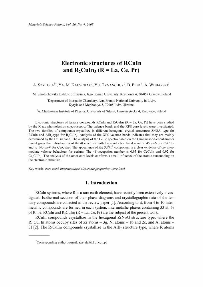
Materials Science-Poland, Vol. 26, No. 4, 2008
Electronic structures of RCuIn and R2CuIn3 (R = La, Ce, Pr)
A. SZYTUŁA1*, YA. M. KALYCHAK2, YU. TYVANCHUK2, B. PENC1, A. WINIARSKI3
1M. Smoluchowski Institute of Physics, Jagiellonian University, Reymonta 4, 30-059 Cracow, Poland 2Department of Inorganic Chemistry, Ivan Franko National University in Liviv,
Kyryla and Mephodiya 5, 79005 Lviv, Ukraine 3A. Chełkowski Institute of Physics, University of Silesia, Uniwersytecka 4, Katowice, Poland
Electronic structures of ternary compounds RCuIn and R2CuIn3 (R = La, Ce, Pr) have been studied by the X-ray photoelectron spectroscopy. The valence bands and the XPS core levels were investigated. The two families of compounds crystallize in different hexagonal crystal structures: ZrNiAl-type for RCuIn and AlB2-type for R2CuIn3. Analysis of the XPS valence bands indicates that they are mainly determined by the Cu 3d band. The analysis of the Ce 3d spectra based on the Gunnarsson-Schönhammer model gives the hybridization of the 4f electrons with the conduction band equal to 45 meV for CeCuIn and to 140 meV for Ce2CuIn3. The appearance of the 3d94f 0 component is a clear evidence of the inter-mediate valence behaviour for cerium. The 4f occupation number is 0.95 for CeCuIn and 0.92 for Ce2CuIn3. The analysis of the other core levels confirms a small influence of the atomic surrounding on the electronic structure.
Key words: rare earth intermetallics; electronic properties; core level
1. Introduction
RCuIn systems, where R is a rare earth element, have recently been extensively inves-tigated. Isothermal sections of their phase diagrams and crystallographic data of the ter-nary compounds are collected in the review paper [1]. According to it, from 4 to 10 inter-metallic compounds are formed in each system. Intermetallic phases containing 33 at. % of R, i.e. RCuIn and R2CuIn3 (R = La, Ce, Pr) are the subject of the present work.
RCuIn compounds crystallize in the hexagonal ZrNiAl structure type, where the R, Cu, In atoms occupy sites of Zr atoms – 3g, Ni atoms – 1b and 2c, and Al atoms – 3f [2]. The R2CuIn3 compounds crystallize in the AlB2 structure type, where R atoms __________
*Corresponding author, e-mail: [email protected]
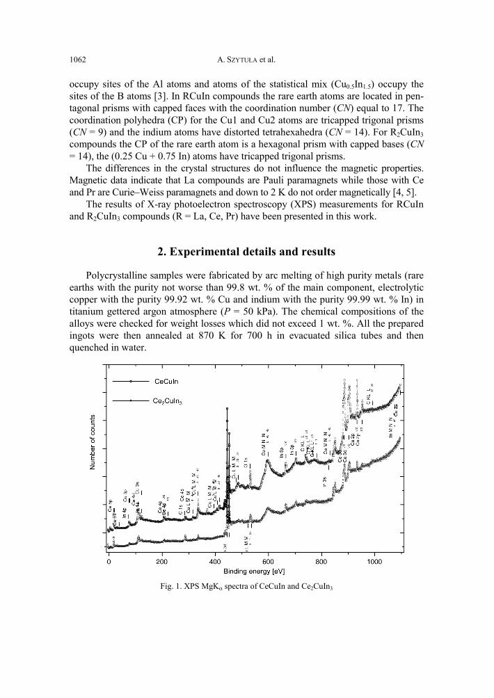
A. SZYTUŁA et al. 1062
occupy sites of the Al atoms and atoms of the statistical mix (Cu0.5In1.5) occupy the sites of the B atoms [3]. In RCuIn compounds the rare earth atoms are located in pen-tagonal prisms with capped faces with the coordination number (CN) equal to 17. The coordination polyhedra (CP) for the Cu1 and Cu2 atoms are tricapped trigonal prisms (CN = 9) and the indium atoms have distorted tetrahexahedra (CN = 14). For R2CuIn3 compounds the CP of the rare earth atom is a hexagonal prism with capped bases (CN = 14), the (0.25 Cu + 0.75 In) atoms have tricapped trigonal prisms.
The differences in the crystal structures do not influence the magnetic properties. Magnetic data indicate that La compounds are Pauli paramagnets while those with Ce and Pr are Curie–Weiss paramagnets and down to 2 K do not order magnetically [4, 5].
The results of X-ray photoelectron spectroscopy (XPS) measurements for RCuIn and R2CuIn3 compounds (R = La, Ce, Pr) have been presented in this work.
2. Experimental details and results
Polycrystalline samples were fabricated by arc melting of high purity metals (rare earths with the purity not worse than 99.8 wt. % of the main component, electrolytic copper with the purity 99.92 wt. % Cu and indium with the purity 99.99 wt. % In) in titanium gettered argon atmosphere (P = 50 kPa). The chemical compositions of the alloys were checked for weight losses which did not exceed 1 wt. %. All the prepared ingots were then annealed at 870 K for 700 h in evacuated silica tubes and then quenched in water.
Fig. 1. XPS MgKα spectra of CeCuIn and Ce2CuIn3
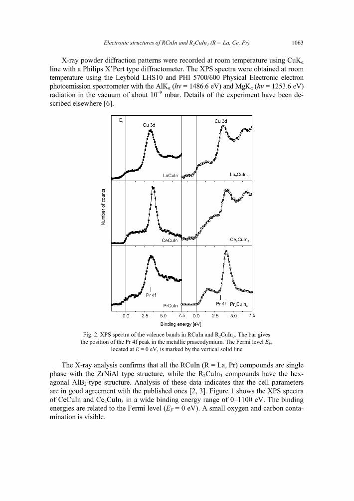
Electronic structures of RCuIn and R2CuIn3 (R = La, Ce, Pr) 1063
X-ray powder diffraction patterns were recorded at room temperature using CuKα line with a Philips X’Pert type diffractometer. The XPS spectra were obtained at room temperature using the Leybold LHS10 and PHI 5700/600 Physical Electronic electron photoemission spectrometer with the AlKα (hν = 1486.6 eV) and MgKα (hν = 1253.6 eV) radiation in the vacuum of about 10–9 mbar. Details of the experiment have been de-scribed elsewhere [6].
Fig. 2. XPS spectra of the valence bands in RCuIn and R2CuIn3. The bar gives the position of the Pr 4f peak in the metallic praseodymium. The Fermi level EF,
located at E = 0 eV, is marked by the vertical solid line
The X-ray analysis confirms that all the RCuIn (R = La, Pr) compounds are single phase with the ZrNiAl type structure, while the R2CuIn3 compounds have the hex-agonal AlB2-type structure. Analysis of these data indicates that the cell parameters are in good agreement with the published ones [2, 3]. Figure 1 shows the XPS spectra of CeCuIn and Ce2CuIn3 in a wide binding energy range of 0–1100 eV. The binding energies are related to the Fermi level (EF = 0 eV). A small oxygen and carbon conta-mination is visible.
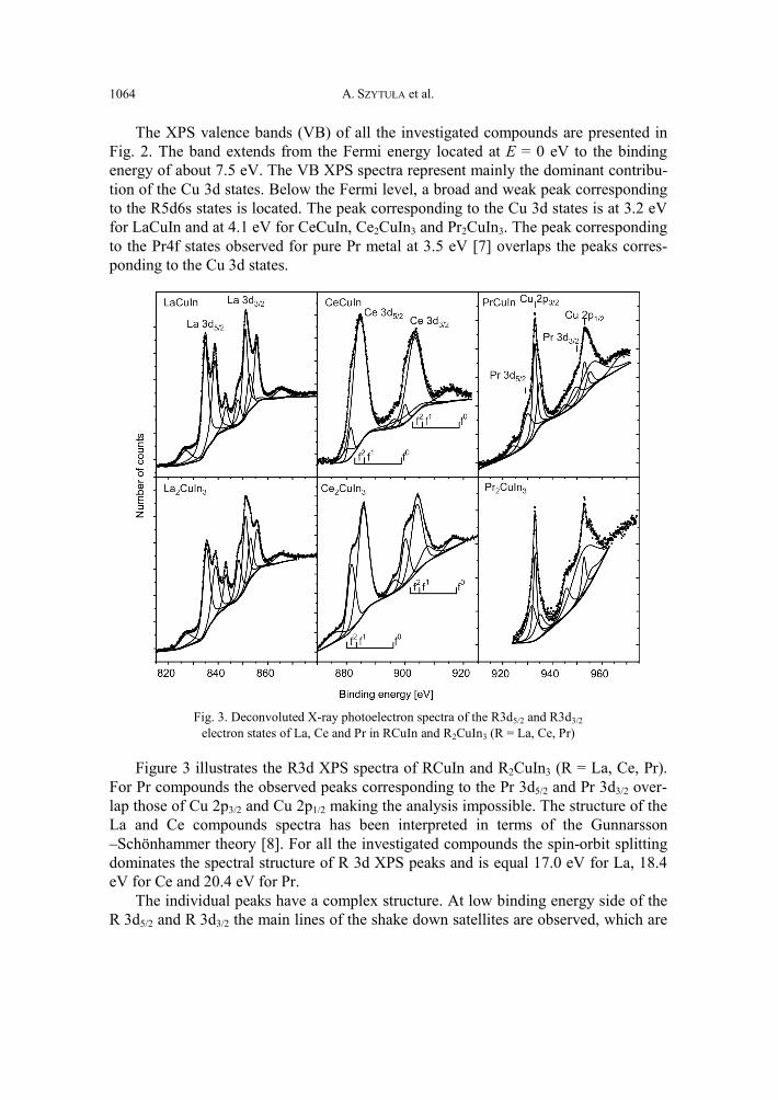
A. SZYTUŁA et al. 1064
The XPS valence bands (VB) of all the investigated compounds are presented in Fig. 2. The band extends from the Fermi energy located at E = 0 eV to the binding energy of about 7.5 eV. The VB XPS spectra represent mainly the dominant contribu-tion of the Cu 3d states. Below the Fermi level, a broad and weak peak corresponding to the R5d6s states is located. The peak corresponding to the Cu 3d states is at 3.2 eV for LaCuIn and at 4.1 eV for CeCuIn, Ce2CuIn3 and Pr2CuIn3. The peak corresponding to the Pr4f states observed for pure Pr metal at 3.5 eV [7] overlaps the peaks corres-ponding to the Cu 3d states.
Fig. 3. Deconvoluted X-ray photoelectron spectra of the R3d5/2 and R3d3/2 electron states of La, Ce and Pr in RCuIn and R2CuIn3 (R = La, Ce, Pr)
Figure 3 illustrates the R3d XPS spectra of RCuIn and R2CuIn3 (R = La, Ce, Pr). For Pr compounds the observed peaks corresponding to the Pr 3d5/2 and Pr 3d3/2 over-lap those of Cu 2p3/2 and Cu 2p1/2 making the analysis impossible. The structure of the La and Ce compounds spectra has been interpreted in terms of the Gunnarsson –Schönhammer theory [8]. For all the investigated compounds the spin-orbit splitting dominates the spectral structure of R 3d XPS peaks and is equal 17.0 eV for La, 18.4 eV for Ce and 20.4 eV for Pr.
The individual peaks have a complex structure. At low binding energy side of the R 3d5/2 and R 3d3/2 the main lines of the shake down satellites are observed, which are
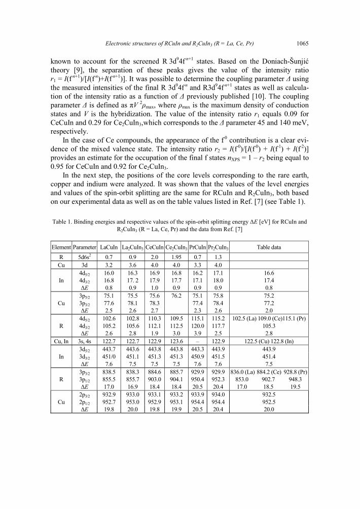
Electronic structures of RCuIn and R2CuIn3 (R = La, Ce, Pr) 1065
known to account for the screened R 3d94f n+1 states. Based on the Doniach-Šunjić theory [9], the separation of these peaks gives the value of the intensity ratio r1 = I(f n+1)/[I(f n)+I(f n+1)]. It was possible to determine the coupling parameter Δ using the measured intensities of the final R 3d94f n and R3d94f n+1 states as well as calcula-tion of the intensity ratio as a function of Δ previously published [10]. The coupling parameter Δ is defined as πV 2ρmax, where ρmax is the maximum density of conduction states and V is the hybridization. The value of the intensity ratio r1 equals 0.09 for CeCuIn and 0.29 for Ce2CuIn3,which corresponds to the Δ parameter 45 and 140 meV, respectively.
In the case of Ce compounds, the appearance of the f 0 contribution is a clear evi-dence of the mixed valence state. The intensity ratio r2 = I(f 0)/[I(f 0) + I(f 1) + I(f 2)] provides an estimate for the occupation of the final f states nXPS = 1 – r2 being equal to 0.95 for CeCuIn and 0.92 for Ce2CuIn3.
In the next step, the positions of the core levels corresponding to the rare earth, copper and indium were analyzed. It was shown that the values of the level energies and values of the spin-orbit splitting are the same for RCuIn and R2CuIn3, both based on our experimental data as well as on the table values listed in Ref. [7] (see Table 1).
Table 1. Binding energies and respective values of the spin-orbit splitting energy ΔE [eV] for RCuIn and R2CuIn3 (R = La, Ce, Pr) and the data from Ref. [7]
Element Parameter LaCuIn La2CuIn3 CeCuIn Ce2CuIn3 PrCuIn Pr2CuIn3 Table data R 5d6s2 0.7 0.9 2.0 1.95 0.7 1.3 Cu 3d 3.2 3.6 4.0 4.0 3.3 4.0
In 4d5/2 16.0 16.3 16.9 16.8 16.2 17.1 16.6 4d3/2 16.8 17. 2 17.9 17.7 17.1 18.0 17.4 ΔE 0.8 0.9 1.0 0.9 0.9 0.9 0.8
Cu 3p5/2 75.1 75.5 75.6 76.2 75.1 75.8 75.2 3p3/2 77.6 78.1 78.3 77.4 78.4 77.2 ΔE 2.5 2.6 2.7 2.3 2.6 2.0
R 4d5/2 102.6 102.8 110.3 109.5 115.1 115.2 102.5 (La) 109.0 (Ce)115.1 (Pr) 4d3/2 105.2 105.6 112.1 112.5 120.0 117.7 105.3 ΔE 2.6 2.8 1.9 3.0 3.9 2.5 2.8
Cu, In 3s, 4s 122.7 122.7 122.9 123.6 – 122.9 122.5 (Cu) 122.8 (In)
In 3d5/2 443.7 443.6 443.8 443.8 443.3 443.9 443.9 3d3/2 451/0 451.1 451.3 451.3 450.9 451.5 451.4 ΔE 7.6 7.5 7.5 7.5 7.6 7.6 7.5
R 3p3/2 838.5 838.3 884.6 885.7 929.9 929.9 836.0 (La) 884.2 (Ce) 928.8 (Pr) 3p1/2 855.5 855.7 903.0 904.1 950.4 952.3 853.0 902.7 948.3 ΔE 17.0 16.9 18.4 18.4 20.5 20.4 17.0 18.5 19.5
Cu 2p3/2 932.9 933.0 933.1 933.2 933.9 934.0 932.5 2p1/2 952.7 953.0 952.9 953.1 954.4 954.4 952.5 ΔE 19.8 20.0 19.8 19.9 20.5 20.4 20.0
A. SZYTUŁA et al. 1066
3. Discussion and summary
The results of the XPS measurements indicate that in two series of the RCuIn and R2CuIn3 compounds the electronic structures are similar. This is in agreement with the magnetic data. In both systems, the magnetic moments of R3+ ions do not order down to 2 K for R = Ce and Pr or order antiferromagnetically for other rare earth elements. For all the compounds we have observed a narrowing of the Cu 3d peaks and their shift to higher binding energies (see Table 2).
Table 2. Values of the level energies and ΓFWHM [eV] of Cu 3d peak in RCuIn and R2CuIn3 (R = La, Ce, Pr) and in pure Cu
Compound E(Cu 3d) ΓFWHM LaCuIn La2CuIn CeCuIn
Ce2CuIn3 PrCuIn
Pr2CuIn3 Cu
4.2 3.6 4.0 4.0 3.4 4.0 3.0
1.0 1.6 1.6 1.3 1.6 1.1 2.4
These results indicate the more localized the 3d states. The analysis of the core le-
vels for various elements gives information about the chemical shift which originates from the changes of the potential related to the formation of the compound. As a re-sult, the binding energies of electronic levels are different in compounds and in pure elements.
Table 3. Binding energy shifts ΔE [eV] of core levels with respect to pure elements
Level LaCuIn La2CuIn3 CeCuIn Ce2CuIn3 PrCuIn Pr2CuIn3 Cu 3d
Cu 3p5/2 Cu 2p3/2 In 4d5/2 In 3d5/2 R 4d5/2 R 3p3/2
0.2 –0.1 0.4
–0.6 –0.2 0.1 2.5
0.6 0.3 0.5
–0.3 –0.3 0.3 2.8
1.0 0.4 0.6 0.3
–0.1 1.3 0.4
1.0 1.0 0.7
–0.2 –0.1 0.5 1.5
0.4 –0.1 1.4
–0.4 –0.6
0 1.1
1.0 0.6 1.5 0.5 0
0.1 1.1
Table 3 shows the chemical shifts of the most pronounced photoemission lines. In
majority of the cases, the positive shift is observed for R = La, Ce, Pr and Cu and neg-ative for indium. The negative shift on the In site may be related to some charge trans-fer towards these atoms.
Acknowledgements
This work was partially supported by the Ministry of Science and Education, Poland under the grant No. 1P03B 111 29.
Electronic structures of RCuIn and R2CuIn3 (R = La, Ce, Pr) 1067
References
[1] KALYCHAK YA.M., Izv Akad. Nauk USSR, Metally, 4 (1998), 110 (in Russian). [2] WIGHT A.E., Proc. of 12th Rare Earth Research Conference, Colorado, 1 (1976), 480. [3] BARANYAK V.M., DMYTRAKH O.V., KALYCHAK YA.M., ZAVALIJ P.YU., Izv. Akad. Nauk USSR,
Inorg. Mater., 24 (1988), 873. [4] SZYTUŁA A., TYVANCHUK YU., JAWORSKA-GOŁĄB T., ZARZYCKI A., KALYCHAK YA., GONDEK Ł.,
STÜSSER N., Chem. Met. Alloys, 1 (2008), 97. [5] SIOURIS I.M., SEMITELOU J.P., YAKINTHOS J.K., J. Alloys Comp., 297 (2000), 26. [6] SZYTUŁA A., JEZIERSKI A., PENC B., FUS D., J. Magn. Magn. Mater., 222 (2000), 47. [7] HÜFNER S., Photoemission Spectroscopy, Springer, Berlin, 1994, p. 435. [8] GUNNARSON O., SCHÖNHAMMER K., Phys. Rev. B, 28 (1983), 4315. [9] DONIACH S., ŠUNJIĆ M., J. Phys. C, 3 (1970), 285.
[10] FUGGLE J.C., HILLEBRECHT F.U., ŻOŁNIEREK Z., LÄSSER R., FREIBURG CH., GUNNARSON O., SCHÖNHAMMER K., Phys. Rev. B, 27 (1983), 4313.
Received 7 May 2007
Materials Science-Poland, Vol. 26, No. 4, 2008
Effect of randomness on anomalous Hall coefficient in antiferromagnet U2PdGa3
V. H. TRAN* Institute of Low Temperature and Structure Research, Polish Academy of Sciences,
50-950 Wrocław, P.O. Box 1014, Poland
The Hall effect has been studied in antiferromagnet U2PdGa3. In the paramagnetic state, the Hall data can be interpreted in terms of skew scattering theory for heavy fermion systems. We observe a large contribution of anomalous Hall coefficient, indicating a dominating contribution of incoherent skew scattering by uranium 5f moments. An interesting behaviour of the RH(T) dependence is found at low temperatures: the RH(T) curve displays a plateau between T* = 12 K and TN = 33 K, followed by a shoul-der upon further decreasing temperature. The appearance of the anomaly around T* suggests the existence of a new scattering mechanism, in addition to well known skew and jump-side scatterings. We compare the Hall data of U2PdGa3 with those observed for strongly correlated electron systems and with those of spin-glasses. Like the latter systems, non-zero spin chirality seems to play a considerable role in the anomalous Hall effect of U2PdGa3.
Key words: U2PdGa3; Hall effect; strongly correlated electron systems; randomness; spin chirality
1. Introduction
U2PdGa3 is an orthorhombic, collinear antiferromagnet with the Néel temperature TN ≈ 33 K [1, 2]. In this compound, there is a competition between the Kondo effect and ran-domness for long-range antiferromagnetism. The Kondo effect manifests itself in electrical resistivity, magnetoresistance properties at high temperatures and causes an enhancement in the electronic heat capacity at low temperatures (γ0 = 72 mJ/(mol·K2). Furthermore, like in many other compounds with randomness, the specific heat of U2PdGa3 does not show a mean-field discontinuity at the Néel temperature but, instead, the dc magnetic susceptibility exhibits magnetic history phenomena. As a result, the antiferromagnetic state with the ordered moments of about 0.3 μB exists only with finite magnetic corre-lation lengths (below 150 Å) [2].
The measurement of the Hall effect is one of the tools of studying scattering mechanisms of conduction electrons on magnetic moments in metals. For ordinary __________
*E-mail: [email protected]
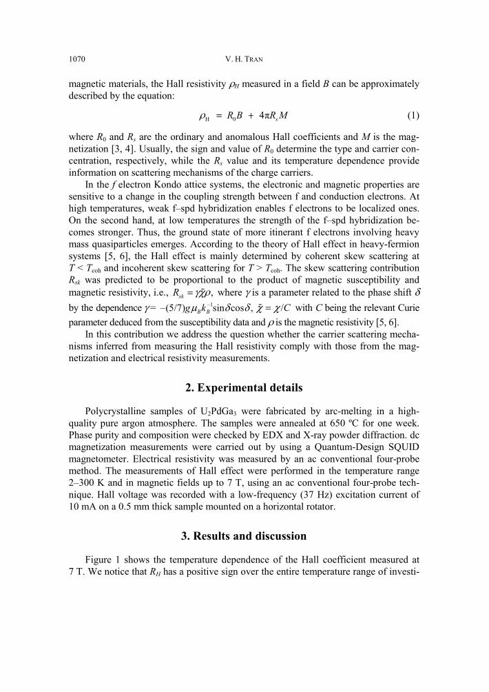
V. H. TRAN 1070
magnetic materials, the Hall resistivity ρH measured in a field B can be approximately described by the equation:
H 0 4π sR B R Mρ = + (1)
where R0 and Rs are the ordinary and anomalous Hall coefficients and M is the mag-netization [3, 4]. Usually, the sign and value of R0 determine the type and carrier con-centration, respectively, while the Rs value and its temperature dependence provide information on scattering mechanisms of the charge carriers.
In the f electron Kondo attice systems, the electronic and magnetic properties are sensitive to a change in the coupling strength between f and conduction electrons. At high temperatures, weak f–spd hybridization enables f electrons to be localized ones. On the second hand, at low temperatures the strength of the f–spd hybridization be-comes stronger. Thus, the ground state of more itinerant f electrons involving heavy mass quasiparticles emerges. According to the theory of Hall effect in heavy-fermion systems [5, 6], the Hall effect is mainly determined by coherent skew scattering at T < Tcoh and incoherent skew scattering for T > Tcoh. The skew scattering contribution Rsk was predicted to be proportional to the product of magnetic susceptibility and magnetic resistivity, i.e., ,skR γχρ= where γ is a parameter related to the phase shift δ by the dependence γ = –1–(5/7) sin cos ,B Bg kμ δ δ /Cχ χ= with C being the relevant Curie parameter deduced from the susceptibility data and ρ is the magnetic resistivity [5, 6].
In this contribution we address the question whether the carrier scattering mecha-nisms inferred from measuring the Hall resistivity comply with those from the mag-netization and electrical resistivity measurements.
2. Experimental details
Polycrystalline samples of U2PdGa3 were fabricated by arc-melting in a high-quality pure argon atmosphere. The samples were annealed at 650 ºC for one week. Phase purity and composition were checked by EDX and X-ray powder diffraction. dc magnetization measurements were carried out by using a Quantum-Design SQUID magnetometer. Electrical resistivity was measured by an ac conventional four-probe method. The measurements of Hall effect were performed in the temperature range 2–300 K and in magnetic fields up to 7 T, using an ac conventional four-probe tech-nique. Hall voltage was recorded with a low-frequency (37 Hz) excitation current of 10 mA on a 0.5 mm thick sample mounted on a horizontal rotator.
3. Results and discussion
Figure 1 shows the temperature dependence of the Hall coefficient measured at 7 T. We notice that RH has a positive sign over the entire temperature range of investi-
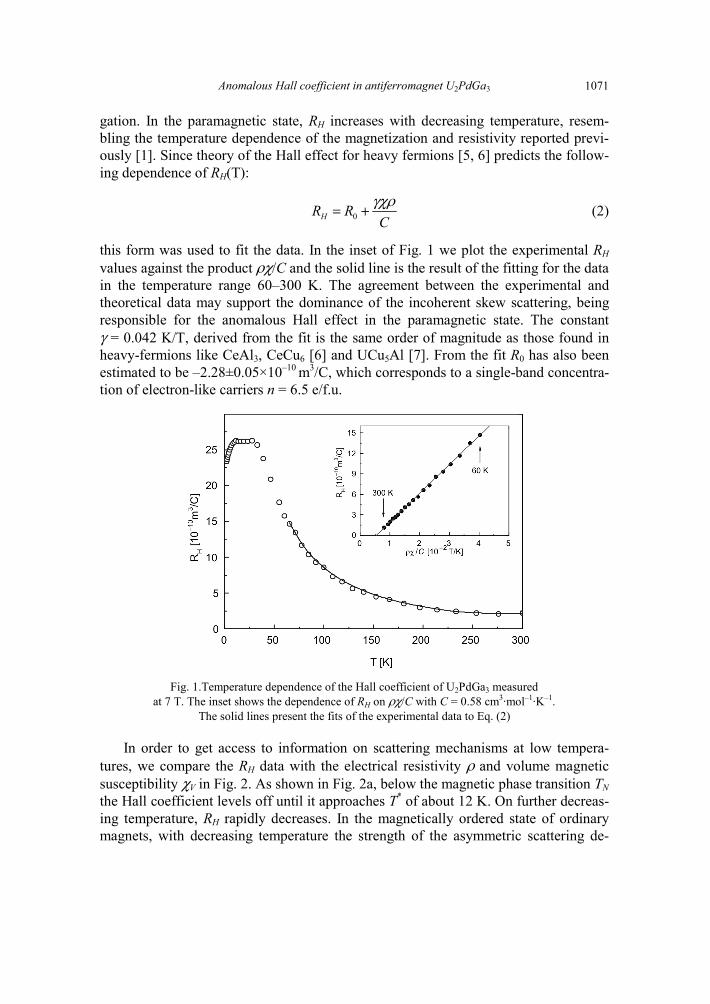
Anomalous Hall coefficient in antiferromagnet U2PdGa3 1071
gation. In the paramagnetic state, RH increases with decreasing temperature, resem-bling the temperature dependence of the magnetization and resistivity reported previ-ously [1]. Since theory of the Hall effect for heavy fermions [5, 6] predicts the follow-ing dependence of RH(T):
0HR RC
γχρ= + (2)
this form was used to fit the data. In the inset of Fig. 1 we plot the experimental RH values against the product ρχ/C and the solid line is the result of the fitting for the data in the temperature range 60–300 K. The agreement between the experimental and theoretical data may support the dominance of the incoherent skew scattering, being responsible for the anomalous Hall effect in the paramagnetic state. The constant γ = 0.042 K/T, derived from the fit is the same order of magnitude as those found in heavy-fermions like CeAl3, CeCu6 [6] and UCu5Al [7]. From the fit R0 has also been estimated to be –2.28±0.05×10⁻¹⁰ m3/C, which corresponds to a single-band concentra-tion of electron-like carriers n = 6.5 e/f.u.
Fig. 1.Temperature dependence of the Hall coefficient of U2PdGa3 measured at 7 T. The inset shows the dependence of RH on ρχ/C with C = 0.58 cm3·mol–1·K–1.
The solid lines present the fits of the experimental data to Eq. (2)
In order to get access to information on scattering mechanisms at low tempera-tures, we compare the RH data with the electrical resistivity ρ and volume magnetic susceptibility χV in Fig. 2. As shown in Fig. 2a, below the magnetic phase transition TN the Hall coefficient levels off until it approaches T* of about 12 K. On further decreas-ing temperature, RH rapidly decreases. In the magnetically ordered state of ordinary magnets, with decreasing temperature the strength of the asymmetric scattering de-
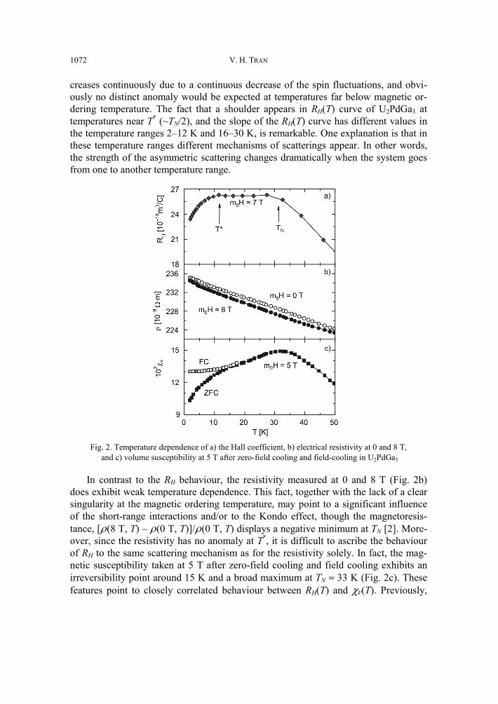
V. H. TRAN 1072
creases continuously due to a continuous decrease of the spin fluctuations, and obvi-ously no distinct anomaly would be expected at temperatures far below magnetic or-dering temperature. The fact that a shoulder appears in RH(T) curve of U2PdGa3 at temperatures near T* (~TN/2), and the slope of the RH(T) curve has different values in the temperature ranges 2–12 K and 16–30 K, is remarkable. One explanation is that in these temperature ranges different mechanisms of scatterings appear. In other words, the strength of the asymmetric scattering changes dramatically when the system goes from one to another temperature range.
Fig. 2. Temperature dependence of a) the Hall coefficient, b) electrical resistivity at 0 and 8 T,
and c) volume susceptibility at 5 T after zero-field cooling and field-cooling in U2PdGa3
In contrast to the RH behaviour, the resistivity measured at 0 and 8 T (Fig. 2b) does exhibit weak temperature dependence. This fact, together with the lack of a clear singularity at the magnetic ordering temperature, may point to a significant influence of the short-range interactions and/or to the Kondo effect, though the magnetoresis-tance, [ρ(8 T, T) – ρ(0 T, T)]/ρ(0 T, T) displays a negative minimum at TN [2]. More-over, since the resistivity has no anomaly at T*, it is difficult to ascribe the behaviour of RH to the same scattering mechanism as for the resistivity solely. In fact, the mag-netic susceptibility taken at 5 T after zero-field cooling and field cooling exhibits an irreversibility point around 15 K and a broad maximum at TN ≈ 33 K (Fig. 2c). These features point to closely correlated behaviour between RH(T) and χV(T). Previously,
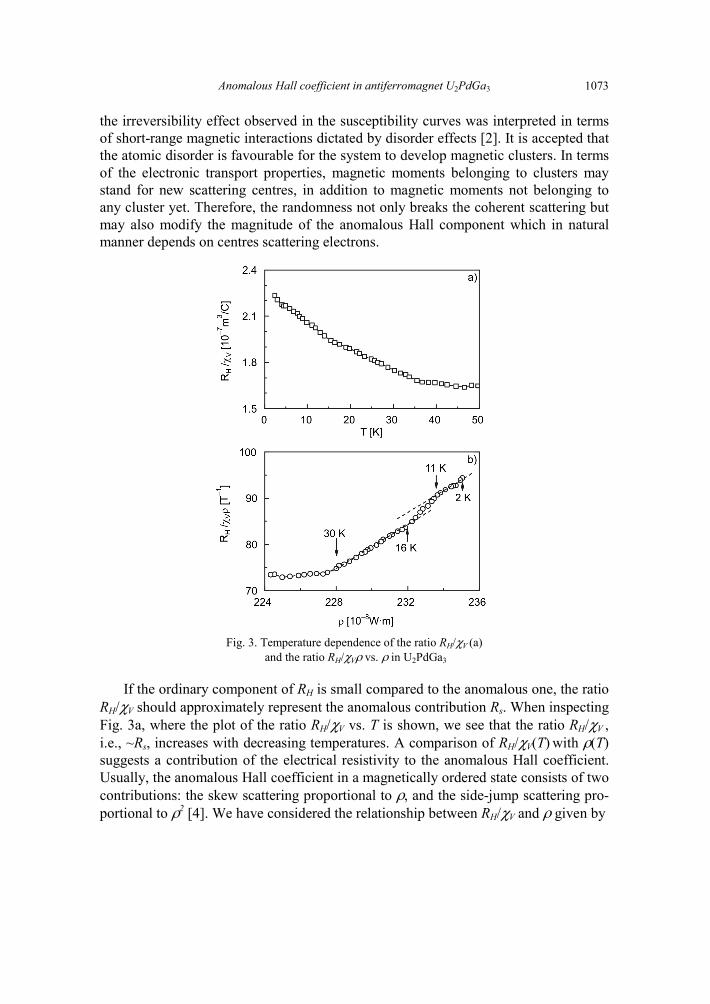
Anomalous Hall coefficient in antiferromagnet U2PdGa3 1073
the irreversibility effect observed in the susceptibility curves was interpreted in terms of short-range magnetic interactions dictated by disorder effects [2]. It is accepted that the atomic disorder is favourable for the system to develop magnetic clusters. In terms of the electronic transport properties, magnetic moments belonging to clusters may stand for new scattering centres, in addition to magnetic moments not belonging to any cluster yet. Therefore, the randomness not only breaks the coherent scattering but may also modify the magnitude of the anomalous Hall component which in natural manner depends on centres scattering electrons.
Fig. 3. Temperature dependence of the ratio RH/χV (a) and the ratio RH/χVρ vs. ρ in U2PdGa3
If the ordinary component of RH is small compared to the anomalous one, the ratio RH/χV should approximately represent the anomalous contribution Rs. When inspecting Fig. 3a, where the plot of the ratio RH/χV vs. T is shown, we see that the ratio RH/χV , i.e., ~Rs, increases with decreasing temperatures. A comparison of RH/χV(T) with ρ(T) suggests a contribution of the electrical resistivity to the anomalous Hall coefficient. Usually, the anomalous Hall coefficient in a magnetically ordered state consists of two contributions: the skew scattering proportional to ρ, and the side-jump scattering pro-portional to ρ2 [4]. We have considered the relationship between RH/χV and ρ given by
V. H. TRAN 1074
2 ~ Hs
V
R R a bρ ρχ
= + (3)
Parameters a and b are the coefficients of the skew and jump-side scattering con-tributions, respectively. According to Eq. (3), a plot Rs/ρ versus ρ should be a straight line, and the coefficients a and b can be deduced. In Figure 3b, the ratio RH/χVρ is plotted in function of ρ. The data indeed approximately lie on a straight line. Interest-ingly, the slopes of the curve RH/χVρ vs. ρ (i.e., parameter b) in the temperature ranges 2–11 K and 16–30 K are the same, suggesting that there is no change in strength of the side-jump scattering across T*, whilst for the skew scattering, the coefficient a (i.e., the intercept of the plot) is different above and below T*. As we have considered above, the formation of magnetic clusters below T* should bring in new scattering centres, yielding additional contribution to skew scattering.
Recently, the chirality mechanism [8] has been proposed as an important mecha-nism for the anomalous Hall effect in spin glass systems [9–12]. Tatara and Kawa-mura [8] have shown that the uniform chirality χ0 contributes to anomalous Hall effect as follows: Rs = (aρ + bρ2) + cχ0. Here, c is a constant relevant to the detailed band structure of the conduction electrons and a uniform chirality χ0 is the sum of the local chirality defined as χijk = Si(SjSk) for three spins Si, Sj and Sk. Clearly, the chirality contribution to Rs is remarkable when the net uniform chirality is finite, i.e., χ0 ≠ 0. In fact, the contribution from χijk to χ0 decays rapidly as exp(–3r/2l)/(kFr)3, where r is the distance between the spins, kF is the Fermi wave number, and l is the mean free path. Thus, one expects a large contribution from χijk to χ0 when the distance between spins r is shorter than l. Using the value of RH and ρ at 2 K, one estimates the mean free path to be 28.6×10⁻¹⁰ m, being larger than the average distance between the spins of the order of 3.5×10⁻¹⁰ m. This means that a number of triangles of three spins may give their contribution to χ0 in the studied compound.
4. Conclusions
We have studied the Hall effect in the short-range antiferromagnet U2PdGa3. The experimental Hall coefficient was compared to the magnetic susceptibility and electri-cal resistivity. From the relationship between RH, χV and ρ, we infer that the incoher-ent skew scattering dominates in the paramagnetic state. Anomalies found in the RH(T) dependence at both the Néel temperature TN ≈ 33 K and T* = 12 K provide a new evi-dence in support that U2PdGa3 is not a classical long-range antiferromagnet. The de-velopment of magnetic clusters below T*, and the resulting randomness have been suggested to cause an anomaly in the RH(T) curve at T*. We considered the observed behaviour to connect with the chiral mechanism of the anomalous Hall effect. We conclude that the low-temperature RH data of U2PdGa3 may be qualitatively under-
Anomalous Hall coefficient in antiferromagnet U2PdGa3 1075
stood in the framework of contributions from the skew, jump-side scatterings and from the spin chirality.
Acknowledgements
This work was supported by Grant No. N202 082 31/0449 from the Ministry of Science and Higher Education, Poland.
References
[1] TRAN V.H., J. Phys. Cond. Matter, 8 (1996), 6267. [2] TRAN V.H., STEGLICH F., ANDRÉ G., Phys. Rev., 65 (2002), 134401. [3] RHYNE J.J., Phys. Rev., 172 (1968), 523. [4] BERGER L., BERGMANN G., [in:] The Hall Effect and Its Applications, C.L. Chien, C.R. Westgate
(Eds.), Plenum, New York, 1980, p. 55. [5] COLEMAN P., ANDERSON P.W., RAMAKRISHNAN T.V., Phys. Rev. Lett., 55 (1985), 414. [6] FERT A., LEVY P.M., Phys. Rev. B, 36 (1987), 1907. [7] TRAN V.H., TROĆ R., STĘPIEŃ-DAMM J., KOMATSUBARA T., STEGLICH F., HAUSER R., BAUER E., Phys.
Rev. B, 66 (2002), 54421. [8] TATARA G., KAWAMURA H., J. Phys. Soc. Japan, 71 (2002), 2613 [9] TAGUCHI Y., OOHARA Y., NAGAOSA N., TOKURA Y., Science, 291 (2001), 2573.
[10] KAGEYAMA T., AITO N., IIKUBO S., SATO M., J. Phys. Soc. Jpn., 72 (2003), 1491. [11] TANIGUCHI T., YAMANAKA K., SUMIOKA H., YAMAZAKI T., TABATA Y., KAWARAZAKI S., Phys. Rev.
Lett., 93 (2004), 246605. [12] YAMANAKA K., TANIGUCHI T., YAMAZAKI T., ASHITAKA N., MORIMOTO Y., TABATA Y., KAWARAZAKI S.,
J. Phys. Cond. Matter, 19 (2007), 145222.
Received 7 May 2007
Materials Science-Poland, Vol. 26, No. 4, 2008
Surface contribution to giant magnetoresistance in Fe/Cr/Fe films
K. WARDA2*, M. PEREIRO1,3, L. WOJTCZAK2, D. BALDOMIR1,3, J. CASTRO1, J. ARIAS3
1Departamento de Física Aplicada, Universidade de Santiago de Compostela, Santiago de Compostela E-15782, Spain
2University of Łódź, Solid State Physics Department, ul. Pomorska 149/153, 92-236 Łódź, Poland 3Instituto de Investigacións Tecnolóxicas, Universidade de Santiago de Compostela,
Santiago de Compostela E-15782, Spain
Transport properties of very thin films have been analysed using the layered potentials calculated by means of the ab initio method represented by the density functional theory (DFT) in the planar geometry for the nFe/3Cr/nFe films, where n is the number of monoatomic Fe layers, (1 ≤ n ≤ 8). We also take into consideration the values of the relaxation time and the effective mass of an electron in terms of the con-sidered potentials. The matching conditions have been applied at the interface and the boundary condi-tions at the surface in order to determine the contributions to the giant magnetoresistance (GMR) coming from the surface, interface, and inner layers. The surface roughness is introduced by means of the specu-larity factor Pσ defined in the spin-dependent terms responsible for the scattering of the electrons. Thus, the electron scattering at the outer surfaces depends on both spin orientations. The main result obtained in the paper is the evaluation that the surface contribution to GMR is very small in comparison with the effect of interface.
Key words: multilayers; giant magnetoresistance; conductivity; thin films
1. Introduction
The giant magnetoresistance (GMR) in multilayers originates from the spin-dependent electron scattering inside a layered structure made of ferromagnetic layers sandwiched between nonmagnetic layers (spacers) and stacked along the direction orthogonal to the layer planes. The electron scattering takes place in each layer, in particular, at non-ideal, rough, and diffusive interfaces and at the outer surfaces of the considered sample [1]. The purpose of the present paper is to investigate the contribu-
__________
*Corresponding author, e-mail: [email protected]
K. WARDA et al. 1078
tion to GMR coming from surfaces, interfaces as well as from inner layers and to compare their influence on the total GMR of the Fe/Cr/Fe sample.
Our considerations are based on the relation between the current of electrons mov-ing in the sample in plane of its surface under the influence of an electric field. The conductivity is then given by the derivative of the current with respect to the applied electric field tending to zero in each monoatomic layer. Thus, the conductivity is of a local character, calculated in the bidimensional space for a planar system embedded into the effective field generated by the interaction between the layered systems. In order to calculate the global value for the conductivity, we sum up all the planar con-tributions in the case of current in plane (CIP) geometry while the case of current per-pendicular to plane (CPP) geometry requires the summation over the local values of the resistivity.
The main advantage of the method used here is a formulation the relation between the electronic current and the applied electric field in a way which allows us to use the input database for a given sample without any fitting or parametrisation. As a source for this purpose, we choose the density functional theory (DFT) whose output data collect the set of the energy eigenvalues, eigenfunctions associated to them and local potential barriers in two dimensional space. Ab initio calculations of the electronic structure for practical reasons were performed by means of the density functional the-ory in the local spin approximation (LSDA). The Kohn–Sham equation was solved using the full potential in the representation of linearized augmented plane wave (FP-LAPW) in a slab geometry [2]. The method is extremely advantageous for computing the electronic structure of multilayers because it was designed to take into account the boundary conditions in the slab geometry for the outer layers remaining in contact with vacuum.
2. Method of calculation and the transport model
The calculations were performed for the slab consisting of 3 films, as shown in Fig. 1. The considered systems are made of 3 Cr monolayers (spacer) in antiferromag-netic ordering sandwiched between two films of nFe monolayers. The magnetization of the ferromagnetic layers is permitted to be parallel or antiparallel depending if an external magnetic field is applied to the sample or not. The electronic structure is cal-culated within the framework of the DFT approach for each monolayers ν in the tri-layered system nFe/3Cr/nFe) bcc (100) with n ranging from 1 up to 8 monolayers. The method of calculation gives the properties of electronic structures that we use as the input for calculating the transport properties described by our model which is based on the Boltzmann formalism. One of the properties that we are able to calculate with our DFT method is the potential barrier distribution Vνσ in which the charge carriers are embedded. A detailed description and the physical origin of the Vνσ parameter can be found in Ref. [3].
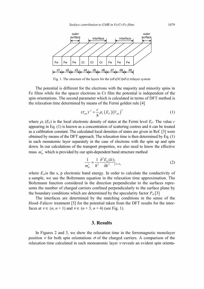
Surface contribution to GMR in Fe/Cr/Fe films 1079
Fig. 1. The structure of the layers for the (nFe|3Cr|nFe) trilayer system
The potential is different for the electrons with the majority and minority spins in Fe films while for the spacer electrons in Cr film the potential is independent of the spin orientations. The second parameter which is calculated in terms of DFT method is the relaxation time determined by means of the Fermi golden rule [4]
( )( )21( ) Fc E Vνσ ν νστ ρ− = (1)
where ρν (EF) is the local electronic density of states at the Fermi level EF. The value c appearing in Eq. (1) is known as a concentration of scattering centres and it can be treated as a calibration constant. The calculated local densities of states are given in Ref. [3] were obtained by means of the DFT approach. The relaxation time is then determined by Eq. (1) in each monatomic layer separately in the case of electrons with the spin up and spin down. In our calculations of the transport properties, we also need to know the effective mass mσ
∗ which is provided by our spin-dependent band structure method
2
2 2
1 1 ( )Fk k
E km k
σ
σ=∗
∂=∂
(2)
where Eσ is the s, p electronic band energy. In order to calculate the conductivity of a sample, we use the Boltzmann equation in the relaxation time approximation. The Boltzmann function considered in the direction perpendicular to the surfaces repre-sents the number of charged carriers confined perpendicularly to the surface plane by the boundary conditions which are determined by the specularity factor Pσ [3]
The interfaces are determined by the matching conditions in the sense of the Hood–Falicov treatment [5] for the potential taken from the DFT results for the inter-faces at ν ∈ (n, n + 1) and ν ∈ (n + 3, n + 4) (see Fig. 1).
3. Results
In Figures 2 and 3, we show the relaxation time in the ferromagnetic monolayer position ν for both spin orientations σ of the charged carriers. A comparison of the relaxation time calculated in each monoatomic layer ν reveals an evident spin orienta-
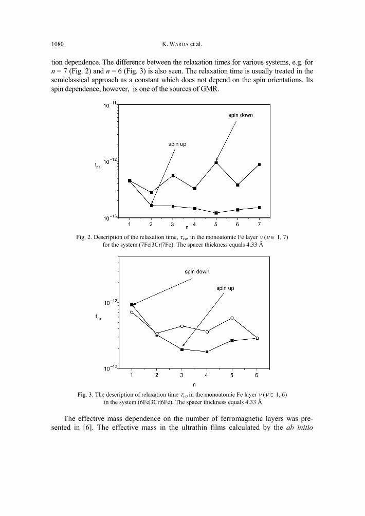
K. WARDA et al. 1080
tion dependence. The difference between the relaxation times for various systems, e.g. for n = 7 (Fig. 2) and n = 6 (Fig. 3) is also seen. The relaxation time is usually treated in the semiclassical approach as a constant which does not depend on the spin orientations. Its spin dependence, however, is one of the sources of GMR.
Fig. 2. Description of the relaxation time, τνσ, in the monoatomic Fe layer ν (ν ∈ 1, 7) for the system (7Fe|3Cr|7Fe). The spacer thickness equals 4.33 Å
Fig. 3. The description of relaxation time τνσ in the monoatomic Fe layer ν (ν ∈ 1, 6)
in the system (6Fe|3Cr|6Fe). The spacer thickness equals 4.33 Å
The effective mass dependence on the number of ferromagnetic layers was pre-sented in [6]. The effective mass in the ultrathin films calculated by the ab initio
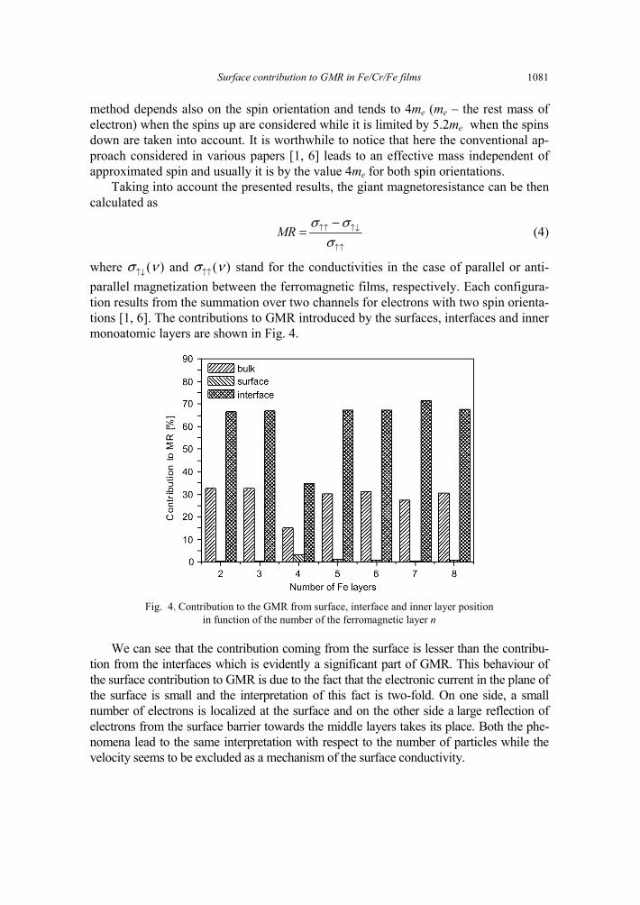
Surface contribution to GMR in Fe/Cr/Fe films 1081
method depends also on the spin orientation and tends to 4me (me – the rest mass of electron) when the spins up are considered while it is limited by 5.2me when the spins down are taken into account. It is worthwhile to notice that here the conventional ap-proach considered in various papers [1, 6] leads to an effective mass independent of approximated spin and usually it is by the value 4me for both spin orientations.
Taking into account the presented results, the giant magnetoresistance can be then calculated as
MRσ σ
σ↑↑ ↑↓
↑↑
−= (4)
where ( )σ ν↑↓ and ( )σ ν↑↑ stand for the conductivities in the case of parallel or anti-parallel magnetization between the ferromagnetic films, respectively. Each configura-tion results from the summation over two channels for electrons with two spin orienta-tions [1, 6]. The contributions to GMR introduced by the surfaces, interfaces and inner monoatomic layers are shown in Fig. 4.
Fig. 4. Contribution to the GMR from surface, interface and inner layer position
in function of the number of the ferromagnetic layer n
We can see that the contribution coming from the surface is lesser than the contribu-tion from the interfaces which is evidently a significant part of GMR. This behaviour of the surface contribution to GMR is due to the fact that the electronic current in the plane of the surface is small and the interpretation of this fact is two-fold. On one side, a small number of electrons is localized at the surface and on the other side a large reflection of electrons from the surface barrier towards the middle layers takes its place. Both the phe-nomena lead to the same interpretation with respect to the number of particles while the velocity seems to be excluded as a mechanism of the surface conductivity.
K. WARDA et al. 1082
4. Conclusions
First of all, our calculations show that the influence of the surface on the GMR is small when compared with the average value per monoatomic layer in the case of the system which we consider here. In contrast, the influence of the interface on GMR is evidently significant, twice greater when compared with the average value of GMR inside the sample. In this context our results confirm the experimental observations [7] and by this fact they reflect an important role of the interface behaviour for GMR de-scription which is known in literature (e.g., [1, 5, 8]). The mechanism now established is connected with the interface potential for the electron spin dependent scattering. The bulk scattering is taken into account by introducing the spin dependent relaxation times in each monoatomic layer. In the case of semiclassical models, the number of parameters becomes so high that the formulas can only be used for a quantitative in-terpretation. The parameters like the relaxation time, the effective mass and the values of the potential barrier are frequently used in the literature. Nobody gives, however, numerical estimation of these parameters despite the fact that they play an important role in GMR evaluation.
Using the results obtained from DFT, we estimate the parameters which we intro-duce in the considerations. Thus, we estimate the contributions to GMR from the sur-faces and interface layers. We can also conclude that the local values of the potential barriers depend not only on the local position of a layer (ν dependence) by also on the thickness of the total film (n dependence).
References
[1] BARNAŚ J., FUSS A., CAMLEY R., GRUMBERG P., ZINN W., Phys, Rev. B, 42 (1990), 8110; BARNAŚ J., BRUYNSERAEDE Y., Phys. Rev. B, 53 (1996), 5449.
[2] WEINERT M., J. Math. Phys., 22 (1981), 2433. [3] PEREIRO M., BALDOMIR D., WARDA K., WOJTCZAK L., J. Phys.: Cond. Matter., 19 (2007), 106210. [4] KUBLER J., Theory of Itinerant Electron Magnetism, Clarendon Press, Oxford, 2000. [5] HOOD R., FALICOV L., Phys. Rev. B, 46 (1992), 8287. [6] WARDA K., WOJTCZAK L., BALDOMIR D., PEREIRO M., ARIAS J., Phys. Stat. Sol. (c), 3 (2006), 73. [7] SANTAMARIA J., GOMEZ M.-E., CYRILLE M.-C., LEIGHTON C., KRISHNAN KANNAN M., SCHULLER I. K.,
Phys. Rev. B, 65 (2001), 12412. [8] CAMLEY R., BARNAŚ J., Phys. Rev. Lett., 63 (1989), 664; BARNAŚ J., BRUYNSERAEDE Y., Europhys.
Lett., 32 (1995), 167.
Received 7 May 2007 Revised 21 September 2007
Materials Science-Poland, Vol. 26, No. 4, 2008
Influence of external magnetic field on transport properties of a quantum dot attached
to non-collinearly polarized magnetic electrodes
M. WAWRZYNIAK*
Department of Physics, Adam Mickiewicz University, ul. Umułtowska 85, 61-614 Poznań, Poland
Transport properties of a single level quantum dot attached to non-collinearly polarized magnetic leads and under the influence of external magnetic field have been analyzed theoretically. Description of the considered system has been modelled by the Anderson Hamiltonian with the finite Coulomb repulsion parameter. The analysis has been performed using the equation of motion method for the non-equilibrium Green function within the Hartree–Fock approximation. Numerical illustration of the transport properties such as differential conductance, tunnelling magnetoresistance and spin accumulation on the dot under influence of external magnetic field has been presented.
Key words: quantum dot; Hartree–Fock approximation; spin accumulation; tunnelling magnetoresistance
I. Introduction
Spin polarized transport through quantum dots attached to ferromagnetic leads has recently raised a great interest. It is not only because of possible area of studying new physical phenomena but also due to promising applications in spinelectronics or mi-croelectronic devices as well as for storage and processing information.
In this paper, an interacting single level quantum dot has been studied. The dot is coupled symmetrically to external ferromagnetic electrodes whose magnetic moments are, in general, non-collinear and may be rotated independently [1–4], the dot being under the influence of an external magnetic field. The orientation of the magnetic moments of the electrodes and direction of the external magnetic field is such that they all are in a common plane.
Further considerations are focused on the bias dependence of the differential con-ductance, tunnel magnetoresistance effect (TMR) and spin accumulation under the
__________
*E-mail: [email protected] l
M. WAWRZYNIAK 1084
influence of external magnetic field on the dot. Moreover, the dependences of TMR and spin accumulation on the angles between the spin moments of the leads is shown for a few values of the external magnetic field.
2. Model
The system under consideration is an interacting single-level quantum dot attached to ferromagnetic leads with non-collinear magnetizations. Degeneration of the discrete level of the dot is removed by an external magnetic field which is, in general, non-collinear with the magnetizations of the electrodes. The field and magnetizations, however, are in a common plane. The axis z of the reference frame is assumed to be along the field, whereas the net spin moments of the leads are in the xz plane and form the angles φR (right lead) and φL (left lead) with the z axis [1, 3].
The whole system is described by the Anderson-like Hamiltonian of a general form
D TH H H Hαα
= + +∑ (1)
where Hα describes the electrodes
,H a aα α β α β α ββ
ε +
=±
=∑∑ k k kk
(2)
for α = L, R (left and right electrodes, respectively). Here, εαkβ is the energy of an electron with the wave vector k and spin β = + (–) that refers to majority (minority) spins in the electrode α, whereas aα β
+k ( )aα βk stands for the creation (annihilation) operators. The
single-particle energy εα kβ includes the electrostatic energy, 0eeU α
α β α βε ε= +k k , where
e (e < 0) stands for the electron charge, 0α βε k is the single-particle energy for the unbi-
ased system, whereas eU α is the electrostatic potential of the αth electrode. Electro-static potentials /2L
e tU V= and /2Re tU V= − are applied to the left and right electrodes,
respectively with Vt as the transport voltage. The dot is described by the Hamiltonian including the Coulomb interaction term
,D dH c c Un nσσ σ
σε +
↑ ↓= +∑ (3)
where ,cσ+ cσ are the creation and annihilation operators for spins σ =↑ , ↓ , the ar-
rows denote projection of the dot spin on the global quantization z axis, and dσε is the
energy level of the dot for spin σ. The Coulomb repulsion parameter is denoted by U, whereas σσσ ccn += denotes the particle number operator. The Zeeman splitting of the
Quantum dot attached to non-collinearly polarized magnetic electrodes 1085
dot level due to external magnetic field is Z d dΔ ε ε↑ ↓= − , where /2d d Zσε ε Δ= ± is the
energy level of the dot for spin σ. Finally, the tunnelling term HT in the Hamiltonian (1) has the form
cos sin
2 2
sin cos h.c.2 2
T k k k kk
k k k k
H T a T a c
T a T a c
α αα α α α
α
α αα α α α
φ φ
φ φ
+ ++ + − − ↑
+ ++ + − − ↓
⎛⎛ ⎞= −⎜⎜ ⎟⎝ ⎠⎝
⎞⎛ ⎞+ + +⎟⎜ ⎟⎝ ⎠⎠
∑∑ (4)
where Tαkβ stands for the appropriate tunneling matrix element.
3. Method
In order to calculate the quantities of interest, we have applied the equation of mo-tion technique for the Green function of the dot | .G c cσσ σ σ
+′ ′=<< >> In the Hartree
–Fock approximation [4, 5], the current flowing from the αth electrode to the dot is given by the formula
( )( )( )Tr ( ) ( ) ( ) ( )2π
r aie dJ G f G Gα α αε ε ε ε ε
+∞<
−∞
= + −∫ Γ (5)
where 1( )
1 expB
f ek T
αα
ε ε μ= −+
is the Fermi–Dirac distribution function with potentials /2LL e teU eVμ = = and
/2RR e teU eVμ = = − , ( ) ( )r aG G iε η= ± stands for the retarded (advanced) Green func-
tion, and ( )G ε< is the lesser Green function. The matrix Γα is of the form
Γα 0
1 cos sin,
sin 1 cosp p
p pα α α α
α α α α
φ φΓ
φ+⎛ ⎞
= ⎜ ⎟−⎝ ⎠ (6)
where pα denotes polarization of the αth electrode. The coupling between the dot and the leads is given by the formula
2( ) 2π | | ( )k kk
Tαβ α β α βΓ ε δ ε ε= −∑
and ( )αβΓ ε is assumed to be energy independent within the electron bandwidth and
zero otherwise.
M. WAWRZYNIAK 1086
Hence, one may write
0 0 0 0( ) (1 ) with L Rpα α ααΓ ε Γ Γ Γ Γ Γ± ±= = ± = =
In order to perform numerical calculations on the considered Green functions, one needs to find self-consistently the average values of the occupation numbers,
Im ,2πdn c c Gσ σ σ σσ
ε+∞+ <
−∞
< >=< >= ∫ (7)
and
.2πdn c c i Gσσ σ σ σσ
ε+∞+ <
− − −−∞
< >=< >= − ∫ (8)
The differential conductance is defined as Gdiff = dJ/dV where the total current flowing through the system is J = (1/2)(JL – JR), whereas
diff diff
diff
( 0, 0) ( , )TMR( 0, 0)
L R L R
L R
G GG
φ φ φ φφ φ
= = −== =
and the spin accumulation on the dot is ( )/2.zS n n↑ ↓< >= −
2. Numerical results and discussion
In this section, we discuss some numerical results for nonlinear transport, assum-ing empty dot level at equilibrium, εd = 0.1 eV, the Coulomb parameter U = 0.4 eV, temperature T = 100 K, polarization pL = pR = 0.5, Γ0 = 0.01 eV, and the electron bandwidth extending from –3.3 eV to 3.3 eV.
The differential conductance is shown in Figs. 1a and 2a for the parallel configura-tion, φL = φR = 0 (solid line), perpendicular configuration, φL = 0, φR = π/2 (dashed line), and the anti-parallel configuration, φL = 0, φR = π (dotted line). The TMR is pre-sented in Figs. 1b and 2b, whereas the spin accumulation <Sz> in Figs. 1c and 2c. Fig-ure 1 represents the case in the absence of external magnetic field, ΔZ = 0. Figure 2, in turn, corresponds to the case with magnetic field applied to the dot, leading to the Zeeman splitting of ΔZ = 0.2 eV. The differential conductance in the absence of exter-nal magnetic field reveals two peaks, appearing symmetrically for positive as well as negative bias resulting from symmetrical coupling to left and right electrodes. The central peaks correspond to the situation when the Fermi level of the source electrode crosses the dot level εd (first transport window, the dot becomes singly occupied). This enables the current flow through the system and appears as a peak in the differential conductance. The outermost peaks correspond to the situation when the electrochemi-
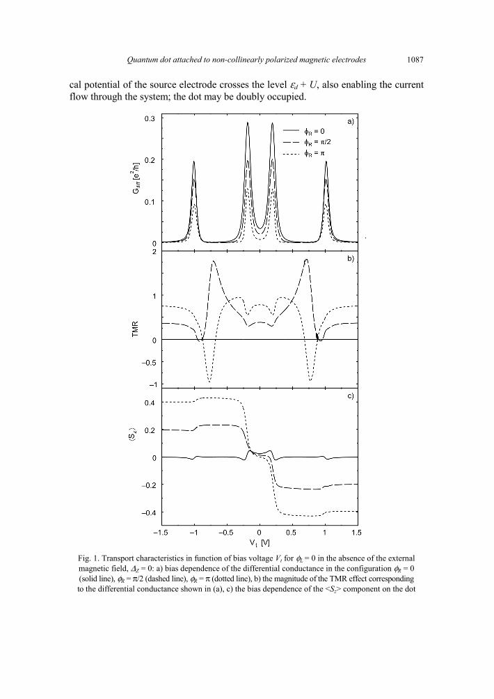
Quantum dot attached to non-collinearly polarized magnetic electrodes 1087
cal potential of the source electrode crosses the level εd + U, also enabling the current flow through the system; the dot may be doubly occupied.
Fig. 1. Transport characteristics in function of bias voltage Vt for φL = 0 in the absence of the external magnetic field, ΔZ = 0: a) bias dependence of the differential conductance in the configuration φR = 0 (solid line), φR = π/2 (dashed line), φR = π (dotted line), b) the magnitude of the TMR effect corresponding to the differential conductance shown in (a), c) the bias dependence of the <Sz> component on the dot
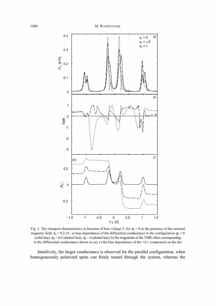
M. WAWRZYNIAK 1088
Fig. 2. The transport characteristics in function of bias voltage Vt for φL = 0 in the presence of the external magnetic field ΔZ = 0.2 eV: a) bias dependence of the differential conductance in the configuration φR = 0
(solid line), φR = π/2 (dashed line), φR = π (dotted line), b) the magnitude of the TMR effect corresponding to the differential conductance shown in (a), c) the bias dependence of the <Sz> component on the dot
Intuitively, the larger conductance is observed for the parallel configuration, when homogeneously polarized spins can freely tunnel through the system, whereas the
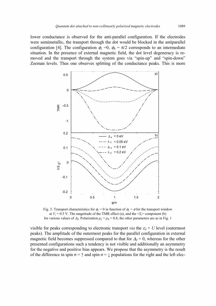
Quantum dot attached to non-collinearly polarized magnetic electrodes 1089
lower conductance is observed for the anti-parallel configuration. If the electrodes were semimetallic, the transport through the dot would be blocked in the antiparallel configuration [4]. The configuration φL =0, φR = π/2 corresponds to an intermediate situation. In the presence of external magnetic field, the dot level degeneracy is re-moved and the transport through the system goes via “spin-up” and “spin-down” Zeeman levels. Thus one observes splitting of the conductance peaks. This is more
Fig. 3. Transport characteristics for φL = 0 in function of φL = φ for the transport window
at Vt = 0.5 V. The magnitude of the TMR effect (a), and the <Sz> component (b) for various values of ΔZ. Polarization pL = pR = 0.8, the other parameters are as in Fig. 1
visible for peaks corresponding to electronic transport via the εd + U level (outermost peaks). The amplitude of the outermost peaks for the parallel configuration in external magnetic field becomes suppressed compared to that for ΔZ = 0, whereas for the other presented configurations such a tendency is not visible and additionally an asymmetry for the negative and positive bias appears. We propose that the asymmetry is the result of the difference in spin σ = ↑ and spin σ = ↓ populations for the right and the left elec-
M. WAWRZYNIAK 1090
trodes when changing the electrode configuration from the parallel to the antiparallel one. Such a behaviour is visible for the d Uε ↑ + and d Uε ↓ + , as well as dε ↑ and dε ↓ spin levels. Moreover, the amplitude of the central peaks in the conductance tends to increase with increasing φR = φ, that is an inverse effect compared to the situation in the absence of external magnetic field.
The plot of TMR effect in function of the bias voltage shows a complex behaviour that is, in general, the result of spin accumulation on the dot, see Figs. 1b, c, 2b, c. In Figure 3a, the angular dependence of the TMR effect is shown for a few values of the external magnetic field and for Vt = 0.5 V. Namely, the magnetization angle of the left electrode is fixed, φL = 0, while the right angle is rotated from φR = 0 to φR = 2π. As one may see, the TMR vanishes for φ = 0 and φ = 2π, for all indicated values of the Zeeman splitting. In the absence of external magnetic field, the TMR is positive at Vt = 0.5 V. One also observes that increasing the external magnetic field leads to nega-tive values of the TMR.
The average ( )/2zS n n↑ ↓< >=< − > component is given in units. As shown in Figs. 1c, 2c and 3b, the absolute value of the average <Sz> increases with increasing the angle φR in the absence as well as in the presence of external magnetic field. Moreover, the <Sz> component is symmetrical with respect to the bias only in a paral-lel configuration, also for the dot under the influence of external magnetic field.
Acknowledgement
This work was supported by funds from the Polish Ministry of Science and Higher Education as a research project in years 2006–2008.
References
[1] WAWRZYNIAK M., GMITRA M., BARNAŚ J., J. Alloys Comp., 423 (2006), 264. [2] SERGUEEV N., SUN Q. -F., GUO H., WANG B. G., WANG J., Phys. Rev. B, 65 (2002), 165303. [3] ŚWIRKOWICZ R., WILCZYŃSKI M., WAWRZYNIAK M., BARNAŚ J., Phys. Rev. B, 73 (2006), 193312. [4] RUDZIŃSKI W., BARNAŚ J., ŚWIRKOWICZ R., WILCZYŃSKI M., Phys. Rev. B, 71 (2005), 205307 . [5] MEIR Y., WINGREEN N. S., Phys. Rev. Lett. 68 (1992), 2512 .
Received 7 May 2007 Revised 30 August 2007
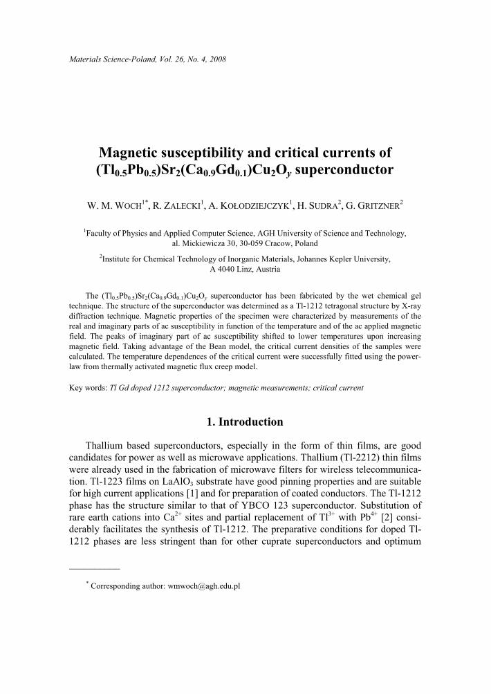
Materials Science-Poland, Vol. 26, No. 4, 2008
Magnetic susceptibility and critical currents of (Tl0.5Pb0.5)Sr2(Ca0.9Gd0.1)Cu2Oy superconductor
W. M. WOCH1*, R. ZALECKI1, A. KOŁODZIEJCZYK1, H. SUDRA2, G. GRITZNER2
1Faculty of Physics and Applied Computer Science, AGH University of Science and Technology, al. Mickiewicza 30, 30-059 Cracow, Poland
2Institute for Chemical Technology of Inorganic Materials, Johannes Kepler University, A 4040 Linz, Austria
The (Tl0.5Pb0.5)Sr2(Ca0.9Gd0.1)Cu2Oy superconductor has been fabricated by the wet chemical gel technique. The structure of the superconductor was determined as a Tl-1212 tetragonal structure by X-ray diffraction technique. Magnetic properties of the specimen were characterized by measurements of the real and imaginary parts of ac susceptibility in function of the temperature and of the ac applied magnetic field. The peaks of imaginary part of ac susceptibility shifted to lower temperatures upon increasing magnetic field. Taking advantage of the Bean model, the critical current densities of the samples were calculated. The temperature dependences of the critical current were successfully fitted using the power-law from thermally activated magnetic flux creep model.
Key words: Tl Gd doped 1212 superconductor; magnetic measurements; critical current
1. Introduction
Thallium based superconductors, especially in the form of thin films, are good candidates for power as well as microwave applications. Thallium (Tl-2212) thin films were already used in the fabrication of microwave filters for wireless telecommunica-tion. Tl-1223 films on LaAlO3 substrate have good pinning properties and are suitable for high current applications [1] and for preparation of coated conductors. The Tl-1212 phase has the structure similar to that of YBCO 123 superconductor. Substitution of rare earth cations into Ca2+ sites and partial replacement of Tl3+ with Pb4+ [2] consi-derably facilitates the synthesis of Tl-1212. The preparative conditions for doped Tl-1212 phases are less stringent than for other cuprate superconductors and optimum
__________
* Corresponding author: [email protected]
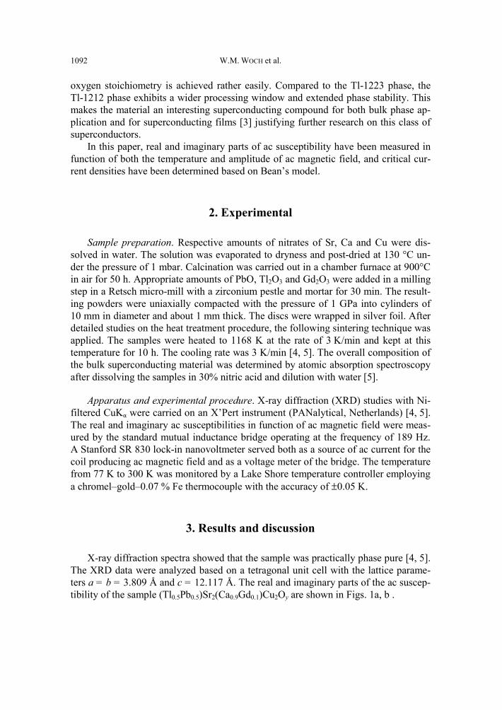
W.M. WOCH et al. 1092
oxygen stoichiometry is achieved rather easily. Compared to the Tl-1223 phase, the Tl-1212 phase exhibits a wider processing window and extended phase stability. This makes the material an interesting superconducting compound for both bulk phase ap-plication and for superconducting films [3] justifying further research on this class of superconductors.
In this paper, real and imaginary parts of ac susceptibility have been measured in function of both the temperature and amplitude of ac magnetic field, and critical cur-rent densities have been determined based on Bean’s model.
2. Experimental
Sample preparation. Respective amounts of nitrates of Sr, Ca and Cu were dis-solved in water. The solution was evaporated to dryness and post-dried at 130 °C un-der the pressure of 1 mbar. Calcination was carried out in a chamber furnace at 900°C
in air for 50 h. Appropriate amounts of PbO, Tl2O3 and Gd2O3 were added in a milling step in a Retsch micro-mill with a zirconium pestle and mortar for 30 min. The result-ing powders were uniaxially compacted with the pressure of 1 GPa into cylinders of 10 mm in diameter and about 1 mm thick. The discs were wrapped in silver foil. After detailed studies on the heat treatment procedure, the following sintering technique was applied. The samples were heated to 1168 K at the rate of 3 K/min and kept at this temperature for 10 h. The cooling rate was 3 K/min [4, 5]. The overall composition of the bulk superconducting material was determined by atomic absorption spectroscopy after dissolving the samples in 30% nitric acid and dilution with water [5].
Apparatus and experimental procedure. X-ray diffraction (XRD) studies with Ni-filtered CuKα were carried on an X’Pert instrument (PANalytical, Netherlands) [4, 5]. The real and imaginary ac susceptibilities in function of ac magnetic field were meas-ured by the standard mutual inductance bridge operating at the frequency of 189 Hz. A Stanford SR 830 lock-in nanovoltmeter served both as a source of ac current for the coil producing ac magnetic field and as a voltage meter of the bridge. The temperature from 77 K to 300 K was monitored by a Lake Shore temperature controller employing a chromel–gold–0.07 % Fe thermocouple with the accuracy of ±0.05 K.
3. Results and discussion
X-ray diffraction spectra showed that the sample was practically phase pure [4, 5]. The XRD data were analyzed based on a tetragonal unit cell with the lattice parame-ters a = b = 3.809 Å and c = 12.117 Å. The real and imaginary parts of the ac suscep-tibility of the sample (Tl0.5Pb0.5)Sr2(Ca0.9Gd0.1)Cu2Oy are shown in Figs. 1a, b .
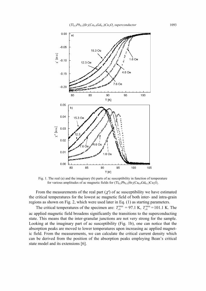
(Tl0.5Pb0.5)Sr2(Ca0.9Gd0.1)Cu2Oy superconductor 1093
Fig. 1. The real (a) and the imaginary (b) parts of ac susceptibility in function of temperature for various amplitudes of ac magnetic fields for (Tl0.5Pb0.5)Sr2(Ca0.9Gd0.1)Cu2Oy
From the measurements of the real part (χ′) of ac susceptibility we have estimated the critical temperatures for the lowest ac magnetic field of both inter- and intra-grain regions as shown on Fig. 2, which were used later in Eq. (1) as starting parameters.
The critical temperatures of the specimen are: inter0cT = 97.1 K, intra
0cT =101.1 K. The ac applied magnetic field broadens significantly the transitions to the superconducting state. This means that the inter-granular junctions are not very strong for the sample. Looking at the imaginary part of ac susceptibility (Fig. 1b), one can notice that the absorption peaks are moved to lower temperatures upon increasing ac applied magnet-ic field. From the measurements, we can calculate the critical current density which can be derived from the position of the absorption peaks employing Bean’s critical state model and its extensions [6].
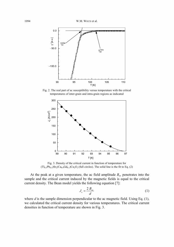
W.M. WOCH et al. 1094
Fig. 2. The real part of ac susceptibility versus temperature with the critical
temperatures of inter-grain and intra-grain regions as indicated
Fig. 3. Density of the critical current in function of temperature for
(Tl0.5Pb0.5)Sr2(Ca0.9Gd0.1)Cu2Oy (full circles). The solid line is the fit to Eq. (2)
At the peak at a given temperature, the ac field amplitude Bac penetrates into the sample and the critical current induced by the magnetic fields is equal to the critical current density. The Bean model yields the following equation [7]:
c2 acBJ
d= (1)
where d is the sample dimension perpendicular to the ac magnetic field. Using Eq. (1), we calculated the critical current density for various temperatures. The critical current densities in function of temperature are shown in Fig. 3.
(Tl0.5Pb0.5)Sr2(Ca0.9Gd0.1)Cu2Oy superconductor 1095
We assumed that the absorption in superconductors is due to thermally activated flux flow [1, 9, 10] which may be described by the following equation:
( ) ( )c cc0
0 1n
TJ T JT
⎡ ⎤= −⎢ ⎥
⎣ ⎦ (2)
where Jc(0) is the critical current density at 0 K, n is the fitting parameter which may vary between 1.3 and 2.0 for high temperature superconductors [10]. Tc0 is the zero-field critical temperature related to inter-granular region of the sample. It has been taken as a starting parameter from real part (χ′) of ac susceptibility as shown in Fig. 2. The fitting of Eq. (2) to the data obtained from experiments is shown in Fig. 3 as the solid line with Tc0 = 96.8±0.3 K being very close to the experimental value inter
0cT
= 97.1 K. The fitting parameters were: n=1.51±0.1 and Jc(0)=(13.4±3)×103 A/cm2. Taking advantage of the fitting parameters, we calculated the critical current density at 77 K: Jc(77) = 1.22×10³ A/cm2. These Jc values are comparable to the critical current densities determined by dc transport measurements in [5]. The fitting exponent n of Eq. (2) is very close to 3/2 which was originally introduced in the superconductive glass state and the giant flux creep model [8, 11].
4. Conclusions
The (Tl0.5Pb0.5)Sr2(Ca0.9Gd0.1)Cu2Oy superconductor has comparable superconduct-ing properties to yttrium based YBCO-123 superconductor. Its inter- and intra-granular critical temperatures are 97.1 K and 101.1 K, respectively. The critical cur-rent density at 77 K is 1.22×10³ A/cm2. Equation (2) fits very well the temperature dependence of critical current with the exponent n equal to 3/2 proving the giant flux creep model.
Acknowledgements
This project was supported by the Faculty of Physics and Applied Computer Science, AGH Univer-sity of Science and Technology, Cracow, Poland and by the Austrian Science Foundation (Fonds zur Förderung der Wissenschaftlichen Forschung in Österreich, project No. 17420-N07).
References
[1] WOCH W.M., ZALECKI R., KOŁODZIEJCZYK A., HEIML O., GRITZNER G., Physica C, 434 (2006), 17. [2] EDGER M., GRITZNER G., Supercond. Sci. Technol., 18 (2005), 87. [3] MALANDRIN G., PERDICARO L.M.S., FRAGALLA I.L., CASSINESE A., PRIGIOBBO A., Physica C,
408–410 (2004), 894. [4] GRITZNER G., SUDRA H., EDER M., J. Phys. Conf. Series 43 (2006) 462. [5] SUDRA H., GRITZNER G., Physica C, 443 (2006), 57. [6] BEAN C.P., Phys. Rev. Lett., 8 (1962), 250.

W.M. WOCH et al. 1096
[7] CLEM J.R., Physica C, 153–155 (1988), 50. [8] YESHURUN Y., MALOZEMOFF A.P., Phys. Rev. Lett., 60 (1988), 2202, [9] TINKHAM M., Phys. Rev. Lett., 61 (1988). 1658.
[10] WOCH W.M., ZALECKI R., KOŁODZIEJCZYK A., CHMIST J., HEIML O., GRITZNER G., Acta Phys. Po-lon. A, 106 (2004) 785.
[11] MÜLLER K.A., TAKASHIGE M., BEDNORZ J.G., Phys. Rev. Lett., 58 (1987), 1143.
Received 7 May 2007 Revised 22 September 2007
Materials Science-Poland, Vol. 26, No. 4, 2008
Magnetoresistive memory in ferromagnetic (Ga,Mn)As nanostructures
T. WOSIŃSKI1*, T. FIGIELSKI1, A. MORAWSKI1, A. MĄKOSA1, R. SZYMCZAK1, J. WRÓBEL1, J. SADOWSKI1, 2
1Institute of Physics, Polish Academy of Sciences, Al. Lotników 32/46, 02-668 Warszawa, Poland 2MAX-Lab, Lund University, 22100 Lund, Sweden
Magneto-resistive nanostructures have been investigated. The structures were fabricated by electron beam lithography patterning and chemical etching from thin epitaxial layers of the ferromagnetic semi-conductor (Ga,Mn)As, in shape of three nanowires joined in one point and forming three-terminal devices, in which an electric current can be driven through any of the three pairs of nanowires. In these devices, a novel magneto-resistive memory effect has been demonstrated, related to a rearrangement of magnetic domain walls between different pairs of nanowires in the device consisting in that its zero-field resistance depends on the direction of previously applied magnetic field. The nanostructures can thus work as two-state devices providing basic elements of nonvolatile memory cells.
Key words: ferromagnetic semiconductor; nanostructure; domain wall; magnetoresistance
1. Introduction
Discoveries of the giant magnetoresistance (GMR) effect [1] and the magnetore-sistance tunnel junction (MTJ) [2] gave rise to the emerging field of magnetoelectron-ics. Based on these phenomena, multilayer devices composed of metallic ferromagnets have been successfully applied for development of magnetic sensors and nonvolatile random access memory cells [3]. On the other hand, recent advance in the low-temperature molecular beam epitaxy (LT-MBE) growth of ferromagnetic semiconduc-tors based on III–V compounds [4] brought about a possibility for integrating elec-tronic and magnetoelectronic devices, providing thus a basis for combining semicon-ductor-based information processing and magnetic-based data storage on the same chip.
__________
*Corresponding author, e-mail: [email protected]
T. WOSIŃSKI et al. 1098
One of the most promising model semiconductors, in this respect, is (Ga,Mn)As, in which a few percent of Ga lattice atoms have been substituted by Mn impurities. Below a magnetic transition temperature, TC, substitutional Mn2+ ions are ferromag-netically ordered owing to the interactions with polarized mobile charge carriers (holes) [5, 6]. The hole density, which is a fraction of the Mn concentration, influences all the magnetic properties of this semiconductor, including both the magnetic anisot-ropy and TC. Although the highest TC in (Ga,Mn)As remains so far below 200 K, it is expected that further optimization of the MBE-growth conditions and post-growth annealing will succeed in obtaining (Ga,Mn)As layers showing room-temperature ferromagnetism [7].
One of the rapidly growing directions of research that includes ferromagnetic semiconductors is the dynamics of individual magnetic domain wall (DW), i.e. a re-gion of inhomogeneous magnetization, separating two ferromagnetic domains of dif-ferent (homogeneous) magnetizations in nanowires [8–10]. In ferromagnetic nanowi- res, the magnetic shape anisotropy, caused by the long-range dipole interaction be-tween localized magnetic moments, usually dominates over an intrinsic anisotropy of crystalline material. Thus, direction of magnetization is forced to be oriented along the wire axis. DW contributes an extra resistance to a wire, and, on the other hand, DW passing through a wire leads to the reversal of the direction of magnetization. Impor-tantly, a DW motion in a wire can be actuated not only by a magnetic field but also by an electric current pulse.
In this paper, we demonstrate a novel magneto-resistive memory effect that ap-pears in lithographically patterned nanowires forming a three-arm nanostructure, fab-ricated from ferromagnetic (Ga,Mn)As layers, and is related to a rearrangement of magnetic DWs between different pairs of nanowires in the structure.
2. Experimental
The nanostructures investigated in this work are junctions of three nanowires joined in one point at the angle of 120° (Fig. 1). That three-arm device (TAD) is frus-trated in the sense that, upon going along any pair of the arms, one meets always with such a pair for which the direction of magnetization is reversed at the junction. In con-sequence, an electric current passing through that pair has to cross a magnetic DW at the junction.
We fabricated the TAD structures from a monocrystalline, 15 nm thick, Ga0.96Mn0.04As layer grown by the LT-MBE method on the (001) face of GaAs sub-strate [11]. Such grown layers suffer from a compressive strain caused by a lattice mismatch on the interface and exhibit an in-plane easy axis of magnetization. The (001) face, being the plane of the layer, has crystalline symmetry of a square, which is not compatible with triangular shape symmetry of the TAD structure. So, all three arms of TAD cannot be fully magnetically equivalent owing to an additional in-plane
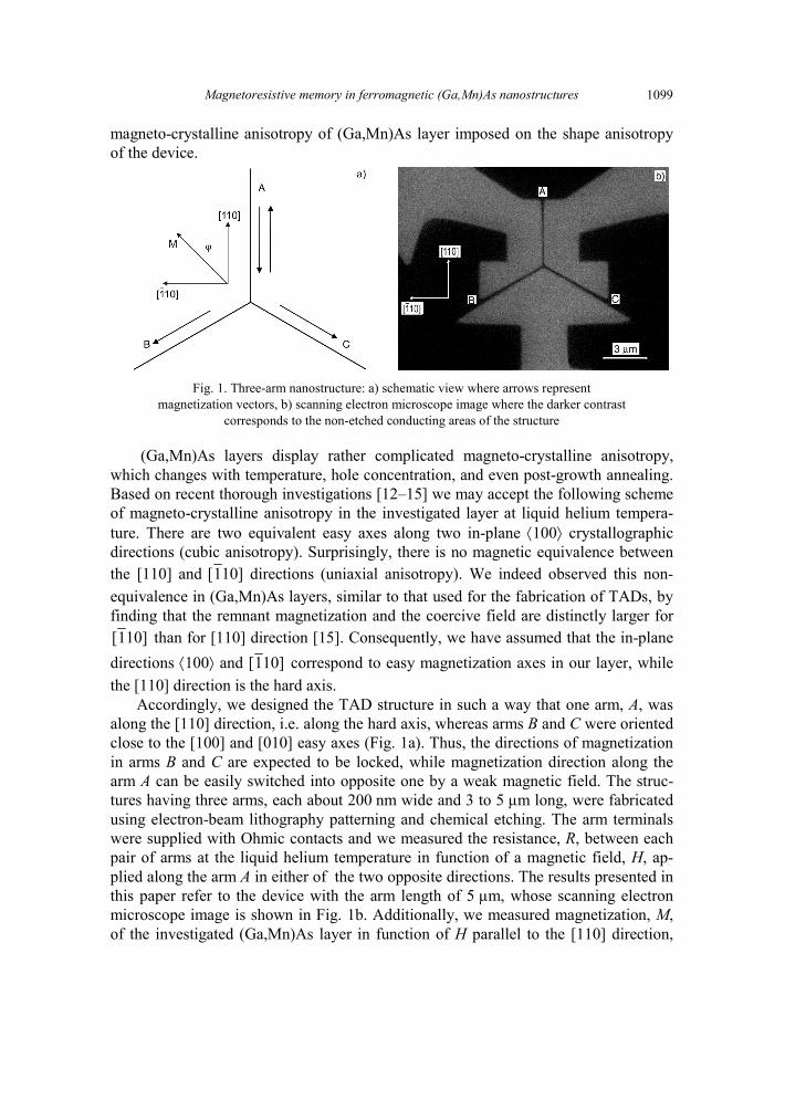
Magnetoresistive memory in ferromagnetic (Ga,Mn)As nanostructures 1099
magneto-crystalline anisotropy of (Ga,Mn)As layer imposed on the shape anisotropy of the device.
Fig. 1. Three-arm nanostructure: a) schematic view where arrows represent magnetization vectors, b) scanning electron microscope image where the darker contrast
corresponds to the non-etched conducting areas of the structure
(Ga,Mn)As layers display rather complicated magneto-crystalline anisotropy, which changes with temperature, hole concentration, and even post-growth annealing. Based on recent thorough investigations [12–15] we may accept the following scheme of magneto-crystalline anisotropy in the investigated layer at liquid helium tempera-ture. There are two equivalent easy axes along two in-plane ⟨100⟩ crystallographic directions (cubic anisotropy). Surprisingly, there is no magnetic equivalence between the [110] and [110] directions (uniaxial anisotropy). We indeed observed this non-equivalence in (Ga,Mn)As layers, similar to that used for the fabrication of TADs, by finding that the remnant magnetization and the coercive field are distinctly larger for [110] than for [110] direction [15]. Consequently, we have assumed that the in-plane directions ⟨100⟩ and [110] correspond to easy magnetization axes in our layer, while the [110] direction is the hard axis.
Accordingly, we designed the TAD structure in such a way that one arm, A, was along the [110] direction, i.e. along the hard axis, whereas arms B and C were oriented close to the [100] and [010] easy axes (Fig. 1a). Thus, the directions of magnetization in arms B and C are expected to be locked, while magnetization direction along the arm A can be easily switched into opposite one by a weak magnetic field. The struc-tures having three arms, each about 200 nm wide and 3 to 5 μm long, were fabricated using electron-beam lithography patterning and chemical etching. The arm terminals were supplied with Ohmic contacts and we measured the resistance, R, between each pair of arms at the liquid helium temperature in function of a magnetic field, H, ap-plied along the arm A in either of the two opposite directions. The results presented in this paper refer to the device with the arm length of 5 μm, whose scanning electron microscope image is shown in Fig. 1b. Additionally, we measured magnetization, M, of the investigated (Ga,Mn)As layer in function of H parallel to the [110] direction,
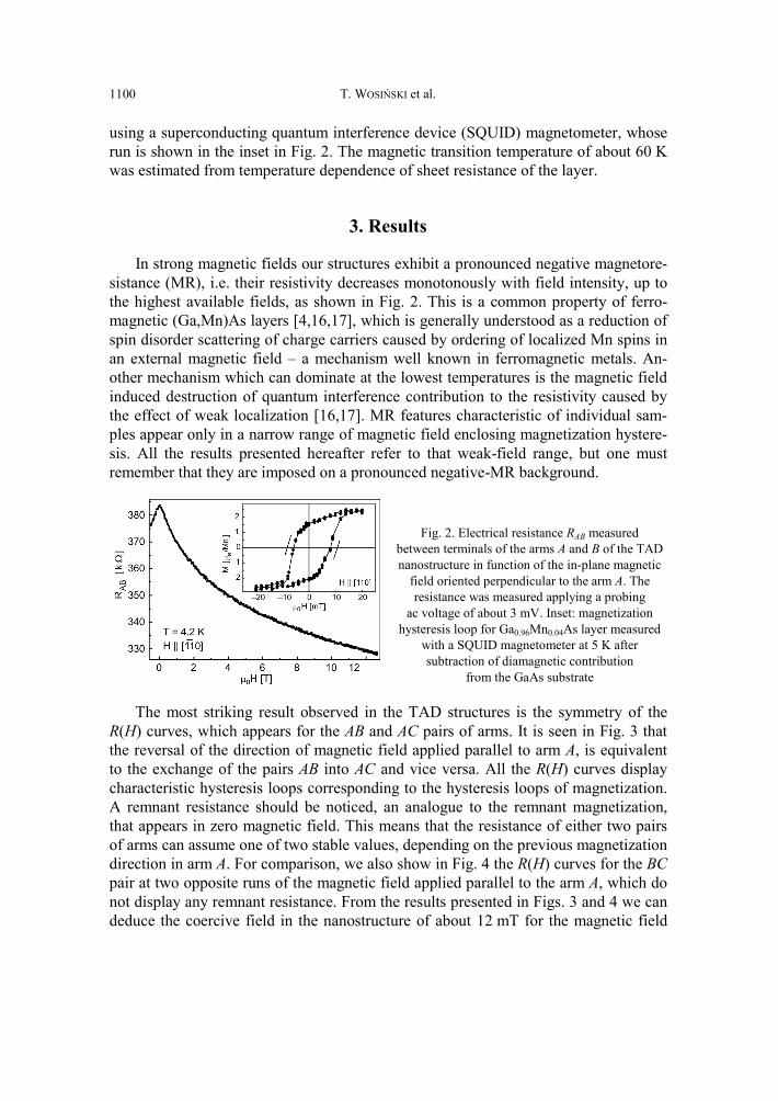
T. WOSIŃSKI et al. 1100
using a superconducting quantum interference device (SQUID) magnetometer, whose run is shown in the inset in Fig. 2. The magnetic transition temperature of about 60 K was estimated from temperature dependence of sheet resistance of the layer.
3. Results
In strong magnetic fields our structures exhibit a pronounced negative magnetore-sistance (MR), i.e. their resistivity decreases monotonously with field intensity, up to the highest available fields, as shown in Fig. 2. This is a common property of ferro-magnetic (Ga,Mn)As layers [4,16,17], which is generally understood as a reduction of spin disorder scattering of charge carriers caused by ordering of localized Mn spins in an external magnetic field – a mechanism well known in ferromagnetic metals. An-other mechanism which can dominate at the lowest temperatures is the magnetic field induced destruction of quantum interference contribution to the resistivity caused by the effect of weak localization [16,17]. MR features characteristic of individual sam-ples appear only in a narrow range of magnetic field enclosing magnetization hystere-sis. All the results presented hereafter refer to that weak-field range, but one must remember that they are imposed on a pronounced negative-MR background.
Fig. 2. Electrical resistance RAB measured between terminals of the arms A and B of the TAD nanostructure in function of the in-plane magnetic
field oriented perpendicular to the arm A. The resistance was measured applying a probing
ac voltage of about 3 mV. Inset: magnetization hysteresis loop for Ga0.96Mn0.04As layer measured
with a SQUID magnetometer at 5 K after subtraction of diamagnetic contribution
from the GaAs substrate
The most striking result observed in the TAD structures is the symmetry of the R(H) curves, which appears for the AB and AC pairs of arms. It is seen in Fig. 3 that the reversal of the direction of magnetic field applied parallel to arm A, is equivalent to the exchange of the pairs AB into AC and vice versa. All the R(H) curves display characteristic hysteresis loops corresponding to the hysteresis loops of magnetization. A remnant resistance should be noticed, an analogue to the remnant magnetization, that appears in zero magnetic field. This means that the resistance of either two pairs of arms can assume one of two stable values, depending on the previous magnetization direction in arm A. For comparison, we also show in Fig. 4 the R(H) curves for the BC pair at two opposite runs of the magnetic field applied parallel to the arm A, which do not display any remnant resistance. From the results presented in Figs. 3 and 4 we can deduce the coercive field in the nanostructure of about 12 mT for the magnetic field
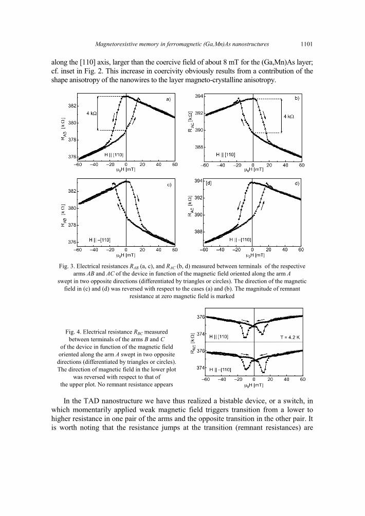
Magnetoresistive memory in ferromagnetic (Ga,Mn)As nanostructures 1101
along the [110] axis, larger than the coercive field of about 8 mT for the (Ga,Mn)As layer; cf. inset in Fig. 2. This increase in coercivity obviously results from a contribution of the shape anisotropy of the nanowires to the layer magneto-crystalline anisotropy.
Fig. 3. Electrical resistances RAB (a, c), and RAC (b, d) measured between terminals of the respective arms AB and AC of the device in function of the magnetic field oriented along the arm A
swept in two opposite directions (differentiated by triangles or circles). The direction of the magnetic field in (c) and (d) was reversed with respect to the cases (a) and (b). The magnitude of remnant
resistance at zero magnetic field is marked
Fig. 4. Electrical resistance RBC measured between terminals of the arms B and C
of the device in function of the magnetic field oriented along the arm A swept in two opposite
directions (differentiated by triangles or circles). The direction of magnetic field in the lower plot
was reversed with respect to that of the upper plot. No remnant resistance appears
In the TAD nanostructure we have thus realized a bistable device, or a switch, in which momentarily applied weak magnetic field triggers transition from a lower to higher resistance in one pair of the arms and the opposite transition in the other pair. It is worth noting that the resistance jumps at the transition (remnant resistances) are
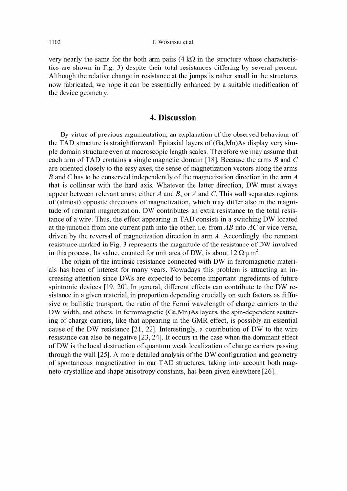
T. WOSIŃSKI et al. 1102
very nearly the same for the both arm pairs (4 kΩ in the structure whose characteris-tics are shown in Fig. 3) despite their total resistances differing by several percent. Although the relative change in resistance at the jumps is rather small in the structures now fabricated, we hope it can be essentially enhanced by a suitable modification of the device geometry.
4. Discussion
By virtue of previous argumentation, an explanation of the observed behaviour of the TAD structure is straightforward. Epitaxial layers of (Ga,Mn)As display very sim-ple domain structure even at macroscopic length scales. Therefore we may assume that each arm of TAD contains a single magnetic domain [18]. Because the arms B and C are oriented closely to the easy axes, the sense of magnetization vectors along the arms B and C has to be conserved independently of the magnetization direction in the arm A that is collinear with the hard axis. Whatever the latter direction, DW must always appear between relevant arms: either A and B, or A and C. This wall separates regions of (almost) opposite directions of magnetization, which may differ also in the magni-tude of remnant magnetization. DW contributes an extra resistance to the total resis-tance of a wire. Thus, the effect appearing in TAD consists in a switching DW located at the junction from one current path into the other, i.e. from AB into AC or vice versa, driven by the reversal of magnetization direction in arm A. Accordingly, the remnant resistance marked in Fig. 3 represents the magnitude of the resistance of DW involved in this process. Its value, counted for unit area of DW, is about 12 Ω·μm2.
The origin of the intrinsic resistance connected with DW in ferromagnetic materi-als has been of interest for many years. Nowadays this problem is attracting an in-creasing attention since DWs are expected to become important ingredients of future spintronic devices [19, 20]. In general, different effects can contribute to the DW re-sistance in a given material, in proportion depending crucially on such factors as diffu-sive or ballistic transport, the ratio of the Fermi wavelength of charge carriers to the DW width, and others. In ferromagnetic (Ga,Mn)As layers, the spin-dependent scatter-ing of charge carriers, like that appearing in the GMR effect, is possibly an essential cause of the DW resistance [21, 22]. Interestingly, a contribution of DW to the wire resistance can also be negative [23, 24]. It occurs in the case when the dominant effect of DW is the local destruction of quantum weak localization of charge carriers passing through the wall [25]. A more detailed analysis of the DW configuration and geometry of spontaneous magnetization in our TAD structures, taking into account both mag-neto-crystalline and shape anisotropy constants, has been given elsewhere [26].
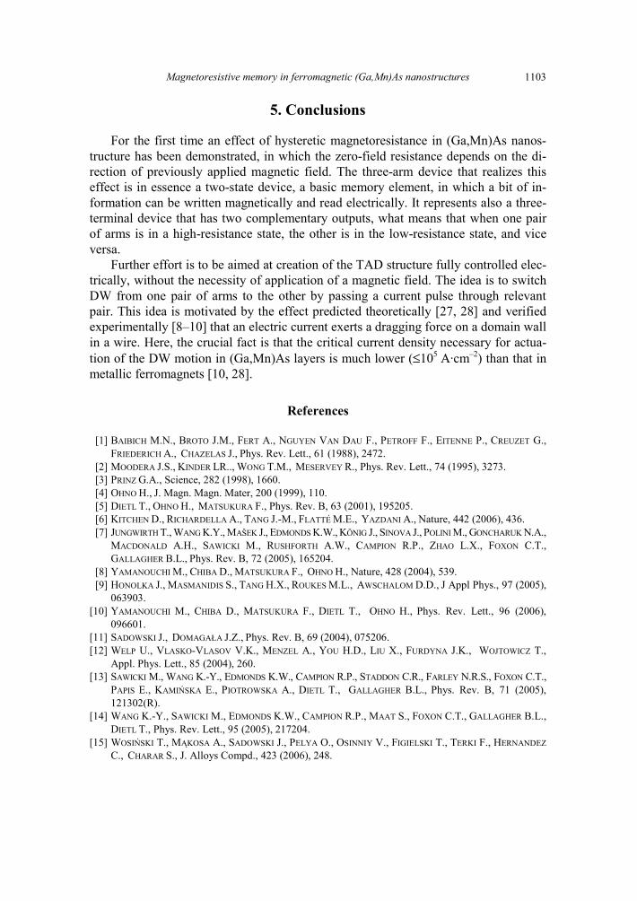
Magnetoresistive memory in ferromagnetic (Ga,Mn)As nanostructures 1103
5. Conclusions
For the first time an effect of hysteretic magnetoresistance in (Ga,Mn)As nanos-tructure has been demonstrated, in which the zero-field resistance depends on the di-rection of previously applied magnetic field. The three-arm device that realizes this effect is in essence a two-state device, a basic memory element, in which a bit of in-formation can be written magnetically and read electrically. It represents also a three-terminal device that has two complementary outputs, what means that when one pair of arms is in a high-resistance state, the other is in the low-resistance state, and vice versa.
Further effort is to be aimed at creation of the TAD structure fully controlled elec-trically, without the necessity of application of a magnetic field. The idea is to switch DW from one pair of arms to the other by passing a current pulse through relevant pair. This idea is motivated by the effect predicted theoretically [27, 28] and verified experimentally [8–10] that an electric current exerts a dragging force on a domain wall in a wire. Here, the crucial fact is that the critical current density necessary for actua-tion of the DW motion in (Ga,Mn)As layers is much lower (≤105 A·cm–2) than that in metallic ferromagnets [10, 28].
References
[1] BAIBICH M.N., BROTO J.M., FERT A., NGUYEN VAN DAU F., PETROFF F., EITENNE P., CREUZET G., FRIEDERICH A., CHAZELAS J., Phys. Rev. Lett., 61 (1988), 2472.
[2] MOODERA J.S., KINDER LR.., WONG T.M., MESERVEY R., Phys. Rev. Lett., 74 (1995), 3273. [3] PRINZ G.A., Science, 282 (1998), 1660. [4] OHNO H., J. Magn. Magn. Mater, 200 (1999), 110. [5] DIETL T., OHNO H., MATSUKURA F., Phys. Rev. B, 63 (2001), 195205. [6] KITCHEN D., RICHARDELLA A., TANG J.-M., FLATTÉ M.E., YAZDANI A., Nature, 442 (2006), 436. [7] JUNGWIRTH T., WANG K.Y., MAŠEK J., EDMONDS K.W., KÖNIG J., SINOVA J., POLINI M., GONCHARUK N.A.,
MACDONALD A.H., SAWICKI M., RUSHFORTH A.W., CAMPION R.P., ZHAO L.X., FOXON C.T., GALLAGHER B.L., Phys. Rev. B, 72 (2005), 165204.
[8] YAMANOUCHI M., CHIBA D., MATSUKURA F., OHNO H., Nature, 428 (2004), 539. [9] HONOLKA J., MASMANIDIS S., TANG H.X., ROUKES M.L., AWSCHALOM D.D., J Appl Phys., 97 (2005),
063903. [10] YAMANOUCHI M., CHIBA D., MATSUKURA F., DIETL T., OHNO H., Phys. Rev. Lett., 96 (2006),
096601. [11] SADOWSKI J., DOMAGAŁA J.Z., Phys. Rev. B, 69 (2004), 075206. [12] WELP U., VLASKO-VLASOV V.K., MENZEL A., YOU H.D., LIU X., FURDYNA J.K., WOJTOWICZ T.,
Appl. Phys. Lett., 85 (2004), 260. [13] SAWICKI M., WANG K.-Y., EDMONDS K.W., CAMPION R.P., STADDON C.R., FARLEY N.R.S., FOXON C.T.,
PAPIS E., KAMIŃSKA E., PIOTROWSKA A., DIETL T., GALLAGHER B.L., Phys. Rev. B, 71 (2005), 121302(R).
[14] WANG K.-Y., SAWICKI M., EDMONDS K.W., CAMPION R.P., MAAT S., FOXON C.T., GALLAGHER B.L., DIETL T., Phys. Rev. Lett., 95 (2005), 217204.
[15] WOSIŃSKI T., MĄKOSA A., SADOWSKI J., PELYA O., OSINNIY V., FIGIELSKI T., TERKI F., HERNANDEZ C., CHARAR S., J. Alloys Compd., 423 (2006), 248.
T. WOSIŃSKI et al. 1104
[16] MATSUKURA F., SAWICKI M., DIETL T., CHIBA D., OHNO H., Physica E, 21 (2004), 1032. [17] PELYA O., WOSIŃSKI T., FIGIELSKI T., MĄKOSA A., MORAWSKI A., SADOWSKI J., DOBROWOLSKI W.,
SZYMCZAK R., WRÓBEL J., TÓTH A.L., J. Alloys Compd., 423 (2006), 252. [18] GOENNENWEIN S.T.B., RUSSO S., MORPURGO A.F., KLAPWIJK T.M., VAN ROY W., DE BOECK J.,
Phys. Rev. B, 71 (2005), 193306. [19] VIGNALE G., FLATTÉ M.E., Phys. Rev. Lett., 89 (2002), 098302. [20] RÜSTER C., BORZENKO T., GOULD C., SCHMIDT G., MOLENKAMP L.W., LIU X., WOJTOWICZ T.J.,
FURDYNA J.K., YU Z.G., FLATTÉ M.E., Phys. Rev. Lett., 91 (2003), 216602. [21] LEVY P.M., ZHANG S., Phys. Rev. Lett., 79 (1997), 5110. [22] CHIBA D., YAMANOUCHI M., MATSUKURA F., DIETL T., OHNO H., Phys. Rev. Lett., 96 (2006),
096602. [23] TANG H.X., MASMANIDIS S., KAWAKAMI R.K., AWSCHALOM D.D., ROUKES M.L., Nature, 431
(2004), 52. [24] WOSIŃSKI T., FIGIELSKI T., PELYA O., MĄKOSA A., MORAWSKI A., SADOWSKI J., DOBROWOLSKI W.,
SZYMCZAK R., WRÓBEL J., Phys. Stat. Sol. (a), 204 (2007), 472. [25] TATARA G., FUKUYAMA H., Phys. Rev. Lett., 78 (1997), 3773. [26] FIGIELSKI T., WOSIŃSKI T., MORAWSKI A., MĄKOSA A., WRÓBEL J., SADOWSKI J., Appl. Phys. Lett.,
90 (2007), 052108. [27] TATARA G., KOHNO H., Phys. Rev. Lett., 92 (2004), 086601. [28] NGUYEN A.K., SKADSEM H.J., BRATAAS A., Phys. Rev. Lett., 98 (2007), 146602.
Received 7 May 2007 Revised 7 September 2007
Contents
B. Idzikowski, MAG-EL-MAT. A summary .................................................................................... 803 H. Szymczak, R. Szymczak, Magnetocaloric effect. Physics and applications ................................. 807 Ł. Gondek, J. Żukrowski, M. Bałanda, D. Kaczorowski, A. Szytuła, Magnetism and electronic
structures of hexagonal 1:1:1 rare earth-based intermetallic compounds ..................................... 815 A. Pikul, D. Kaczorowski, Strong electronic correlations in CePt4In ................................................ 821 M. Urbaniak, NiFe/Au/Co/Au layered films. Magnetic and transport properties .............................. 831 M. Czapkiewicz, J. Kanak, T. Stobiecki, M. Kachel, M. Żołądź, I. Sveklo, A. Maziewski,
S. van Dijken, Micromagnetic properties of Co/Pt multilayers deposited on various buffer layers ...... 839 P. Machnikowski, A. Grodecka, C. Weber, A. Knor, Optical control and decoherence of spin
qubits in quantum dots.................................................................................................................. 851 Z. Wilamowski, H. Malissa, W. Jantsch, Tuning of spin resonance by an electric current in a Si
quantum well ................................................................................................................................ 863 J. Dajka, L. Machura, S. Rogoziński, J. Łuczka, Mesoscopic rings. Multi-states induced by quan-
tum thermal fluctuations ............................................................................................................... 871 W. Rudziński, Phonon-assisted tunnelling through a quantum dot coupled to magnetic leads .......... 879 T. Ślęzak, S. Stankov, M. Zając, M. Ślęzak, K. Matlak, N. Spiridis, B. Laenens, N. Planckaert,
M. Rennhofer, K. Freindl, D. Wilgocka-Ślęzak, R. Rüffer, J. Korecki, Magnetism of ultra-thin iron films seen by the nuclear resonant scattering of synchrotron radiation ................................. 885
W. Stankowski, A. Muszyński, Time of fall and some properties of the Morasko meteorite ............ 897 B. Kozakowski, M. Duda, J. Wolny, Structure of decagonal quasicrystals described by clusters .... 903 Z. Bąk, Fracton mediated superconductivity in the “net fractal” systems. Preliminaries and an
overview of other fracton based models ....................................................................................... 913 O. Volnianska, P. Bogusławski, Electronic and magnetic properties of IIA–V nitrides.................... 921 B. Brodowska, I. Kuryliszyn-Kudelska, M. Arciszewska, K. Dybko, V. Domukhovski,
W. Dobrowolski, V.E. Slynko, E.I. Slynko, V.K. Dugaev, Transport and magnetic properties of Ge1–x–y Mnx(Eu,Yb)yTe semimagnetic semiconductors ............................................................ 927
P. Wiśniewski, Z. Henkie, A. Pietraszko, Crystallization of (Th1–xUx)3As4 ferromagnetic semi-conductor from the Ga flux .......................................................................................................... 933
J. Kaczkowski, A. Jezierski, First-principles study of X/Bi2Te3(0001) surface (X = Ag, Ni, Ti) ..... 939 P. Kamasa, L.K. Varga, P. Myśliński, S.G. Rassolov, V. Maksimov, B. Idzikowski, Crystalliza-
tion of amorphous Fe–Cr–B alloys investigated with high heating rates ...................................... 947 M. Klimczak, E. Talik, J. Jarosz, T. Mydlarz, Properties of GdFeAl ternary compound in two
crystallographic structures ............................................................................................................ 953 W. Knoff, P. Dziawa, V. Osinniy, B. Taliashvili, V. Domukhowski, R. Diduszko, J. Domagała,
E. Łusakowska, R. Jakieła, T. Story, Ferromagnetic and structural properties of Ge1–xMnxTe epitaxial layers .............................................................................................................................. 959
J. W. Kłos, M. Krawczyk, Electronic miniband formation in a two-dimensional semiconductor superlattice ................................................................................................................................... 965
M. Kowalik, Spin torque characteristics for the asymmetric non-collinearly polarized ferromag-netic single-electron devices ......................................................................................................... 971
M. Kowalik, K.W. Wojciechowski, Elastic properties of orientationally disordered crystal of mono- and polydisperse hard dumbbells in three dimensions ...................................................... 977
K. M. Lebecki, Modelling of magnetization reversal for long ferromagnetic nanotubes .................. 983 S. Mamica, H. Puszkarski, Spin-wave theory of spin-polarized electron energy loss spectroscopy.
Measurements in 5 ML Fe film deposited on W(110) .................................................................. 989
1106
A. Szajek, M. Werwiński, J.A. Morkowski, G. Chełkowska, R. Troć, Photoemission spectra of some uranium compounds ............................................................................................................ 995
J. W. Narojczyk, K. W. Wojciechowski, Influence of size polydispersity on the elastic constants of fcc crystals of static soft spheres .............................................................................................. 1001
A. Paja, B. J. Spisak, Conductivity of a disordered ferromagnetic monoatomic film........................ 1009 M. Pugaczowa-Michalska, M. Falkowski, A. Kowalczyk, Ab intio study of YNi4Si under pressure 1015 A. Stupakiewicz, A. Fleurence, R. Gieniusz, A. Maziewski, T. Maroutian, P. Gogol, B. Bartenlian,
R. Mégy, P. Beauvillain, Study of ultrathin Co films grown on Si(111) substrates ..................... 1021 K. Szałowski, T. Balcerzak, Ground state phase diagram of a diluted fcc magnet with modified
RKKY interaction in an external magnetic field .......................................................................... 1027 M. Szot, L. Kowalczyk, E. Smajek, V.V. Volobuev, A.Yu. Sipatov, T. Story, Spectral dependence
of magnetooptical Kerr effect in EuS-based ferromagnetic semiconductor multilayers ............... 1033 T. Szumiata, M. Gzik-Szumiata, K. Brzózka, Pseudodipolar model of surface magnetostriction
for thin layers with roughness ...................................................................................................... 1039 W. Szuszkiewicz, J.-F. Morhange, M. Schumm, M. Lentze, Z. Gołacki, P. Skupiński, K. Grasza,
J. Geurts, Raman spectroscopy of Zn1–xCoxO bulk mixed crystals ............................................... 1045 W. Szuszkiewicz, J.-F. Morhange, E. Dynowska, E. Janik, W.H. Zaleszczyk, A. Presz, J. Z. Domagała,
W. Caliebe, G. Karczewski, T. Wojtowicz, Raman scattering studies of MBE-grown ZnTe nanowires ..................................................................................................................................... 1053
A. Szytuła, Ya.M. Kalychak, Yu. Tyvanchuk, B. Penc, A. Winiarski, Electronic structures of RCuIn and R2CuIn3 (R = La, Ce, Pr) ............................................................................................ 1061
V. H. Tran, Effect of randomness on anomalous Hall coefficient in antiferromagnet U2PdGa3 ........ 1069 K. Warda, M. Pereiro, L. Wojtczak, D. Baldomir, J. Castro, J. Arias, Surface contribution to giant
magnetoresistance in Fe/Cr/Fe films ............................................................................................ 1077 M. Wawrzyniak, Influence of external magnetic field on transport properties of a quantum dot
attached to non-collinearly polarized magnetic electrodes ........................................................... 1083 W. M. Woch, R. Zalecki, A. Kołodziejczyk, H. Sudra, G. Gritzner, Magnetic susceptibility and
critical currents of (Tl0.5Pb0.5)Sr2(Ca0.9Gd0.1)Cu2Oy superconductor ............................................ 1091 T. Wosiński, T. Figielski, A. Morawski, A. Mąkosa, R. Szymczak, J. Wróbel, J. Sadowski,
Magnetoresistive memory in ferromagnetic (Ga, Mn)As nanostructures ..................................... 1097